Embed Size (px)
Citation preview

DESIGN OF A HIGH EFFICIENCY POWER
AMPLIFIER BY USING DOHERTY CONFIGURATION
a thesis
submitted to the department of electrical and
electronics engineering
and the institute of engineering and sciences
of bilkent university
in partial fulfillment of the requirements
for the degree of
master of science
By
KAZIM PEKER
December 2010

I certify that I have read this thesis and that in my opinion it is fully adequate,
in scope and in quality, as a thesis for the degree of Master of Science.
Prof. Dr. Abdullah ATALAR(Supervisor)
I certify that I have read this thesis and that in my opinion it is fully adequate,
in scope and in quality, as a thesis for the degree of Master of Science.
Dr. Tarık REYHAN
I certify that I have read this thesis and that in my opinion it is fully adequate,
in scope and in quality, as a thesis for the degree of Master of Science.
Prof. Dr. Cemal YALABIK
Approved for the Institute of Engineering and Sciences:
Prof. Dr. Levent ONURALDirector of Institute of Engineering and Sciences
ii

ABSTRACT
DESIGN OF A HIGH EFFICIENCY POWER
AMPLIFIER BY USING DOHERTY CONFIGURATION
KAZIM PEKER
M.S. in Electrical and Electronics Engineering
Supervisor: Prof. Dr. Abdullah ATALAR
December 2010
Power amplifiers (PAs) have their highest efficiency when they are used at full
power (0dB back-off). For this reason, most PAs are used at 1dB compression
point (P1dB), but this point is highly nonlinear. For high linearity, PAs should
be used at some back-off value (below the point of 1dB compression point). In
this case the efficiency of PAs decreases drastically.
Another issue is that widely used digital modulation techniques produce sig-
nals which has a large peak-to-average power ratio (PAPR). In modern systems
the power is reduced automatically to use spectrum efficiently and to prevent
interference and detection. These conditions force new PA designs to have both
high linearity and high efficiency from P1dB point down to a few dB back-off
region.
iii
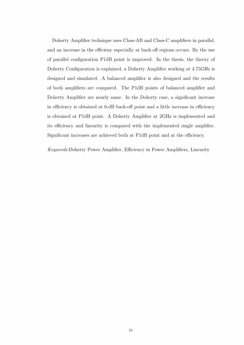
Doherty Amplifier technique uses Class-AB and Class-C amplifiers in parallel,
and an increase in the efficieny especially at back-off regions occurs. By the use
of parallel configuration P1dB point is improved. In the thesis, the theory of
Doherty Configuration is explained, a Doherty Amplifier working at 4.75GHz is
designed and simulated. A balanced amplifier is also designed and the results
of both amplifiers are compared. The P1dB points of balanced amplifier and
Doherty Amplifier are nearly same. In the Doherty case, a significant increase
in efficiency is obtained at 6-dB back-off point and a little increase in efficiency
is obtained at P1dB point. A Doherty Amplifier at 2GHz is implemented and
its efficiency and linearity is compared with the implemented single amplifier.
Significant increases are achieved both at P1dB point and at the efficiency.
Keywords:Doherty Power Amplifier, Efficiency in Power Amplifiers, Linearity
iv

OZET
DOHERTY KONFIGURASYONUNU KULLANARAK YUKSEK
VERIMLI YUKSELTEC TASARIMI
KAZIM PEKER
Elektrik ve Elektronik Muhendisligi Bolumu Yuksek Lisans
Tez Yoneticisi: Prof. Dr. Abdullah ATALAR
Aralık 2010
Yukseltecler maksimum guc seviyesinde kullanıldıkları zaman en yuksek ver-
imliligi gosterirler. Bu nedenle yukseltecler genellikle kazancın 1 dB azaldıgı
noktada (P1dB noktası) kullanılır. Fakat P1dB noktasında yukseltecler, dogrusal
olmayan sekilde calısırlar. Yukselteclerin dogrusal ozellige sahip olması icin, elde
edilebilen en fazla cıkıs gucunun asagısında bir cıkıs gucu elde edilecek sekilde
kullanılması gerekmektedir. Bu durumda ise yukselteclerin verimliliginde ciddi
bir azalma yasanır.
Diger taraftan, yaygın olarak kullanılan dijital modulasyon tekniklerinde
uretilen sinyallerin maksimum guc - ortalama guc oranları oldukca fazladır.
Bunun yanında, modern sistemlerde spektrumu daha az kullanmak ve tespit
edilmeyi engellemek icin, guc otomatik olarak azaltılır. Bu kosullar yeni tasar-
lanan yukselteclerin, P1dB noktasından bu noktanın birkac dB dusuk cıkıs gucu
olan bolgesine kadar yuksek dogrusallıkla birlikte yuksek verimlilige de sahip
olmasını zorunlu hale getirmistir.
v

Doherty Yukselteci, AB ve C sınıflarındaki yukseltecleri parelel olacak sekilde
kullanmaktadır. Boylece, ozellikle back-off bolgelerinde, guc yukselteci sistemi-
nin verimliligi artar. Parelel konfigurasyonunun kullanımı sayesinde P1dB nok-
tası da artar ve dogrusallık artar. Tezde, Doherty Yukselteci yapısının teorisi
acıklanmıs, 4.75GHz’de calısan Doherty Yukselteci tasarlanmıs ve simulasyonu
yapılmıstır. Bununla birlikte, dengelenmis yukseltec tasarımı da yapılmıs ve bu
iki yukseltecin sonucları karsılastırılmıstır. Dengelenmis yukseltecin ve Doherty
yukseltecin P1dB noktaları birbirine oldukca yakındır. 6dB’lik back-off nok-
tasında verimlilikte ciddi bir artıs saglanmıs ve P1dB noktasında da az miktarda
artıs saglanmıstır. Ayrıca 2GHz’de caılsan bir Doherty Yukselteci de uretilerek
karakteristikleri incelenmistir. Bu yukseltecin sonucları ayrı olarak uretilmis olan
tekil yukseltec ile karsılastırılmıs, P1dB noktasında ve verimlilikte artıs oldugu
gozlemlemlenmistir.
Anahtar Kelimeler: Doherty Yukselteci, Yukselteclerdeki Verimlilik, Dogrusallık
vi

ACKNOWLEDGMENTS
I would like to thank my supervisor Prof. Dr. Abdullah Atalar for his supervision
and guidance about the studies for this thesis and also for teaching me both the
theoretical and practical approaches to the engineering problems.
I would also like to thank to Dr. Tarık Reyhan and Prof. Dr. Cemal Yalabık
for reading and commenting on the thesis.
I would like to thank to my fiance Kumsal Ozgun and my sister Meltem Peker
for both helping me in the prepration of this thesis and for their love in whole
my life. Also I would like to give my best gratitude to my parents Fatma and
Faruk Peker for supporting me all my life.
Special thanks to Onur Tanyeri, Akif Alperen Coskun and all my colleagues
at BilUzay that encouraged and helped me with my thesis.
I would also like to thank TUBITAK for the financal support through my
graduate studies.
vii
Contents
1 INTRODUCTION 1
2 RF AMPLIFIERS 5
2.1 Class-A Amplifiers . . . . . . . . . . . . . . . . . . . . . . . . . . 6
2.2 Class-B Amplifiers . . . . . . . . . . . . . . . . . . . . . . . . . . 7
2.3 Class-AB Amplifiers . . . . . . . . . . . . . . . . . . . . . . . . . 9
2.4 Class-C Amplifiers . . . . . . . . . . . . . . . . . . . . . . . . . . 10
2.5 Balanced Amplifiers . . . . . . . . . . . . . . . . . . . . . . . . . . 11
3 THE THEORY OF DOHERTY POWER AMPLIFIER 14
3.1 Effects of Conduction Angle and Input Power to the Efficiency . . 14
3.2 Efficiency Enhancement and Dynamic Load . . . . . . . . . . . . 19
3.3 Doherty Amplifier Configuration . . . . . . . . . . . . . . . . . . . 22
3.3.1 Carrier Amplifier . . . . . . . . . . . . . . . . . . . . . . . 23
3.3.2 Peaking Amplifier . . . . . . . . . . . . . . . . . . . . . . . 23
viii

3.3.3 Matching Circuits . . . . . . . . . . . . . . . . . . . . . . . 23
3.3.4 Impedance Inverting Network . . . . . . . . . . . . . . . . 25
3.3.5 Phase Compensation Network . . . . . . . . . . . . . . . . 26
3.3.6 Impedance Matching Network . . . . . . . . . . . . . . . . 26
3.3.7 Efficiency of Doherty Amplifier . . . . . . . . . . . . . . . 27
3.4 Practical Approaches . . . . . . . . . . . . . . . . . . . . . . . . . 29
4 DESIGN OF AMPLIFIER AND SIMULATION RESULTS 32
4.1 Determining the Bias Points . . . . . . . . . . . . . . . . . . . . . 32
4.2 Carrier Amplifier Design . . . . . . . . . . . . . . . . . . . . . . . 35
4.2.1 Input Matching Circuit Design . . . . . . . . . . . . . . . 35
4.2.2 Output Matching Circuit Design . . . . . . . . . . . . . . 38
4.2.3 Final Circuit with Biasing Circuits and Stability Analysis . 43
4.2.4 Results of Carrier Amplifier . . . . . . . . . . . . . . . . . 44
4.3 Peaking Amplifier Design . . . . . . . . . . . . . . . . . . . . . . . 52
4.3.1 Output Matching Circuit Design . . . . . . . . . . . . . . 52
4.3.2 Results of Peaking Amplifier . . . . . . . . . . . . . . . . . 56
4.4 Combining the Amplifiers . . . . . . . . . . . . . . . . . . . . . . 62
4.4.1 Design of Impedance Matching Network (Combiner) at the
Output . . . . . . . . . . . . . . . . . . . . . . . . . . . . . 62
ix
4.4.2 Phase Compensation Network at the Output of Peaking
Amplifier . . . . . . . . . . . . . . . . . . . . . . . . . . . 63
4.5 Balanced Amplifier Design . . . . . . . . . . . . . . . . . . . . . . 67
4.6 Results of Doherty Amplifier, Balanced Amplifier and Single Car-
rier Amplifier . . . . . . . . . . . . . . . . . . . . . . . . . . . . . 68
5 IMPLEMENTATION AND RESULTS 77
6 CONCLUSIONS 86
x
List of Figures
2.1 Drain Current vs. Drain Voltage with Drain Voltage Swing and
Drain Current Swing Waveforms for Class A Amplifier . . . . . . 6
2.2 Drain Current vs. Drain Voltage with Drain Voltage Swing and
Drain Current Swing Waveforms for Class B Amplifier . . . . . . 8
2.3 Drain Current vs. Drain Voltage with Drain Voltage Swing and
Drain Current Swing Waveforms for Class AB Amplifier . . . . . 9
2.4 Drain Current vs. Drain Voltage with Drain Voltage Swing and
Drain Current Swing Waveforms for Class C Amplifier . . . . . . 10
2.5 Balanced Amplifier Block Diagram . . . . . . . . . . . . . . . . . 13
3.1 Drain Voltage, Drain Current Waveforms for Conduction Angle β 15
3.2 Maximum Achievable Efficiency vs. Conduction Angle . . . . . . 19
3.3 Usage of Additional Voltage Source . . . . . . . . . . . . . . . . . 20
3.4 Usage of Second Amplifier . . . . . . . . . . . . . . . . . . . . . . 21
3.5 Doherty Configuration with Shunt Load . . . . . . . . . . . . . . 22
3.6 Overall Doherty Configuration . . . . . . . . . . . . . . . . . . . 24
xi

3.7 Theoretical Efficiencies of Doherty Amplifier and Class-B Ampli-
fier . . . . . . . . . . . . . . . . . . . . . . . . . . . . . . . . . . 29
3.8 Final Configuration for Doherty Amplifier . . . . . . . . . . . . . 30
4.1 The Circuit that is Used to Plot I-V Traces . . . . . . . . . . . . 33
4.2 I-V Traces for Different Gate Voltages . . . . . . . . . . . . . . . 34
4.3 The Zoomed Version of I-V Traces for Different Gate Voltages . . 34
4.4 Basic Amplifier Circuit to Find the Input Matching . . . . . . . . 35
4.5 Input and Output Impedances of the Amplifier . . . . . . . . . . 36
4.6 Input Matching Circuit . . . . . . . . . . . . . . . . . . . . . . . . 37
4.7 Response of Input Matching Circuit and Input Impedance of Am-
plifier . . . . . . . . . . . . . . . . . . . . . . . . . . . . . . . . . . 37
4.8 Carrier Amplifier Circuit with Input Matching Used in Load-Pull
Analysis . . . . . . . . . . . . . . . . . . . . . . . . . . . . . . . . 38
4.9 Load-Pull Contour Graph for 20dBm Input Power . . . . . . . . . 39
4.10 Load-Pull Contour Graph for 25dBm Input Power . . . . . . . . . 39
4.11 Load-Pull Contour Graph for 30dBm Input Power . . . . . . . . . 39
4.12 Load-Pull Contour Graph for 35dBm Input Power . . . . . . . . . 40
4.13 Output Matching Circuits for Both 25Ω and 50Ω termination . . 41
4.14 Load-Pull Contour Graphs for 20dBm and 35dBm Input Powers
and Responses of Matching Circuits . . . . . . . . . . . . . . . . . 42
xii

4.15 Carrier Amplifier Circuit with the Addition of Output Matching
Circuit . . . . . . . . . . . . . . . . . . . . . . . . . . . . . . . . . 42
4.16 Gain of Carrier Amplifier with Both 25Ω and 50Ω Terminations . 43
4.17 Final Carrier Amplifier Circuit with the Addition of Biasing Cir-
cuits, Stabilization Elements and Real Capacity Models . . . . . . 45
4.18 K and B parameters for Carrier Amplifier . . . . . . . . . . . . . 46
4.19 Large Signal S11 and S21 of Carrier Amplifier with 20dBm Input
Power and 25Ω Termination . . . . . . . . . . . . . . . . . . . . . 47
4.20 Large Signal S11 and S21 of Carrier Amplifier with 30dBm Input
Power and 25Ω Termination . . . . . . . . . . . . . . . . . . . . . 47
4.21 Large Signal S11 and S21 of Carrier Amplifier with 20dBm Input
Power and 50Ω Termination . . . . . . . . . . . . . . . . . . . . . 48
4.22 Large Signal S11 and S21 of Carrier Amplifier with 30dBm Input
Power and 50Ω Termination . . . . . . . . . . . . . . . . . . . . . 48
4.23 Large Signal S11 and S21 of Carrier Amplifier with 34dBm Input
Power and 50Ω Termination . . . . . . . . . . . . . . . . . . . . . 49
4.24 Final Gain of Carrier Amplifier with Both 25Ω and 50Ω Terminations 50
4.25 PAE of Carrier Amplifier with Both 25Ω and 50Ω Terminations . 51
4.26 Drain Efficiency of Carrier Amplifier with Both 25Ω and 50Ω Ter-
minations . . . . . . . . . . . . . . . . . . . . . . . . . . . . . . . 51
4.27 Load-Pull Contour Graphs with 30dBm Input Power and -1.5V
Gate Voltage . . . . . . . . . . . . . . . . . . . . . . . . . . . . . 53
xiii

4.28 Load-Pull Contour Graphs with 35dBm Input Power and -1.5V
Gate Voltage . . . . . . . . . . . . . . . . . . . . . . . . . . . . . 54
4.29 Load-Pull Contour Graphs with 34dBm Input Power and -2.3V
Gate Voltage . . . . . . . . . . . . . . . . . . . . . . . . . . . . . 55
4.30 Output Matching Circuit Of Peaking Amplifier . . . . . . . . . . 56
4.31 Large Signal S11 and S21 of Peaking Amplifier with 20dBm Input
Power and -1.5V Gate Voltage . . . . . . . . . . . . . . . . . . . . 56
4.32 Large Signal S11 and S21 of Peaking Amplifier with 30dBm Input
Power and -1.5V Gate Voltage . . . . . . . . . . . . . . . . . . . . 57
4.33 Large Signal S11 and S21 of Peaking Amplifier with 34dBm Input
Power and -1.5V Gate Voltage . . . . . . . . . . . . . . . . . . . . 58
4.34 Large Signal S11 and S21 of Peaking Amplifier with 30dBm Input
Power and -2.9V Gate Voltage . . . . . . . . . . . . . . . . . . . . 60
4.35 Large Signal S11 and S21 of Peaking Amplifier with 34dBm Input
Power and -2.9V Gate Voltage . . . . . . . . . . . . . . . . . . . . 60
4.36 Large Signal S11 and S21 of Peaking Amplifier with 36dBm Input
Power and -2.9V Gate Voltage . . . . . . . . . . . . . . . . . . . . 61
4.37 Gain Characteristic of the Peaking Amplifier for Different Gate
Bias Points . . . . . . . . . . . . . . . . . . . . . . . . . . . . . . 61
4.38 PAE and Drain Efficiency for Peaking Amplifier with -1.5V Gate
Voltage . . . . . . . . . . . . . . . . . . . . . . . . . . . . . . . . . 62
4.39 PAE and Drain Efficiency for Peaking Amplifier with -2.9V Gate
Voltage . . . . . . . . . . . . . . . . . . . . . . . . . . . . . . . . . 63
xiv

4.40 Input Impedance of Combiner . . . . . . . . . . . . . . . . . . . . 64
4.41 Doherty Amplifier Configuration without the Phase Compensa-
tion Network . . . . . . . . . . . . . . . . . . . . . . . . . . . . . 64
4.42 RF Currents at the Output of Each Amplifier and at the Combined
Branch of Doherty Amplifier without Compensation Network . . . 65
4.43 Final Doherty Amplifier with the Addition of Compensation Line 66
4.44 RF Currents at the Output of Each Amplifier and at the Combined
Branch of Doherty Amplifier with Compensation Transmission Line 66
4.45 Balanced Amplifier Block Diagram . . . . . . . . . . . . . . . . . 67
4.46 Power Gain and Drain Efficiency vs. Output Power with -2V Gate
Voltage for Peaking Amplifier . . . . . . . . . . . . . . . . . . . . 69
4.47 Gain and Drain Efficiency vs. Output Power with -2.5V Gate
Voltage for Peaking Amplifier . . . . . . . . . . . . . . . . . . . . 70
4.48 Power Gain and Drain Efficiency vs. Output Power with -3.3V
Gate Voltage for Peaking Amplifier . . . . . . . . . . . . . . . . . 71
4.49 Power Gain of Carrier, Doherty and Balanced Amplifiers vs. Out-
put Power with -2.9V Gate Voltage for Peaking Amplifier Used at
Doherty Amplifier . . . . . . . . . . . . . . . . . . . . . . . . . . . 71
4.50 Power Gain of Carrier, Doherty and Balanced Amplifiers vs. Input
Power with -2.9V Gate Voltage for Peaking Amplifier Used at
Doherty Amplifier . . . . . . . . . . . . . . . . . . . . . . . . . . . 72
4.51 PAE vs. Output Power for Carrier, Balanced and Doherty Amplifiers 73
xv

4.52 Drain Efficiency vs. Output Power for Carrier, Balanced and Do-
herty Amplifiers . . . . . . . . . . . . . . . . . . . . . . . . . . . . 73
4.53 PAE vs. Back-off for Carrier, Balanced and Doherty Amplifiers . 74
4.54 Drain Efficiency vs. Back-off for Carrier, Balanced and Doherty
Amplifiers . . . . . . . . . . . . . . . . . . . . . . . . . . . . . . . 75
5.1 Output Impedance of Peaking Amplifier at the Combining Point,
the marker 1 shows the value of the impedance . . . . . . . . . . . 78
5.2 Phase Measurement of Carrier Amplifier . . . . . . . . . . . . . . 79
5.3 Phase Measurement of Peaking Amplifier . . . . . . . . . . . . . . 79
5.4 Measured gain of the Doherty Amplifier at Low Power Levels . . . 80
5.5 Measured gain of the Doherty Amplifier at P1dB point . . . . . . 81
5.6 Measured gain of the Single Amplifier at P1dB point . . . . . . . 82
5.7 Measured gain of the Single and the Doherty amplifiers . . . . . . 82
5.8 Power added efficiency of the Single and the Doherty amplifiers . 83
5.9 Drain efficiency of the Single and the Doherty amplifiers . . . . . 83
5.10 Power added efficiency of the Single and the Doherty amplifiers . 84
5.11 Drain efficiency of the Single and the Doherty amplifiers . . . . . 85
xvi

List of Tables
4.1 P1dB for Three Different Configurations . . . . . . . . . . . . . . 70
4.2 Power Added Efficiency (%) . . . . . . . . . . . . . . . . . . . . . 75
4.3 Drain Efficiency (%) . . . . . . . . . . . . . . . . . . . . . . . . . 75
xvii

Dedicated to My Family

Chapter 1
INTRODUCTION
Power amplifier of a wireless system is specified by its bandwidth, its output
power, sensitivity and the operating frequency. Moreover two other concepts, the
linearity and the efficiency define the performance and the quality of the power
amplifier.
P1dB is the point where the gain of an amplifier decreases 1dB due to the
compression. The output power at this point is accepted as the maximum output
power that is amplified linearly. This point is also called as ”0dB back-off” point
where the term ”back-off” indicates the difference between the output power and
P1dB. Above P1dB, the amplifier operates in the saturation region which causes
nonlinearity at the output, the gain response is not flat anymore which causes
improper amplification. Amplitude modulation (AM) is commonly used in most
of modern communication systems. Since a constant gain is aimed for all input
power levels, this point limits the maximum power that can be delivered to the
system. [2] [3]
On the other hand, in some modulation systems very high linearity is desired.
In these cases amplifiers are used in a few dBs back-off region, far away from the
1

nonlinearity region. Thus, P1dB is commonly used as an indication of linearity.
In the thesis, P1dB is used for this purpose as far as an indication of maximum
available output power and back-off region is used to indicate the more linear
region.
Usages of mobile wireless applications increase widely and power amplifiers
basically dominate the battery life, because they are the most power consuming
elements in wireless systems. Increase in power consumption also causes more
heat generation. For these reasons, the efficiency of power amplifiers is very
important not only for mobile systems but for all wireless systems.
The efficiency of an amplifier is measured with two different concepts. The first
one is the drain efficiency which is the indication of what percentage of input
power (from the supply) is converted to output radio frequency (RF) power. The
second one is the power added efficiency (PAE) which is the indication of what
percentage of supply power is converted to RF power gain. In the thesis, both
of these concepts are used to measure the efficiency of the designed amplifier.
Efficiency is dependent to the output power and increases with the increased
output power. Hence, the highest efficiency is obtained at saturation region
where a high nonlinearity occurs. In the back-off region since the output power
is low, efficiency is also very low. In other words, to maintain high efficiency
and high linearity together is the main challenge for power amplifier design. An-
other main issue is to obtain high efficiency at back-off region since AM systems
creates signals with low input power. Moreover, modern modulation techniques
commonly includes AM with high peak-to-average-power ratio.[4] [5]
Under these conditions, in order to increase the efficiency Doherty Configura-
tion can be used. This technique is firstly proposed by William Doherty in 1936:
2

Changing the output load seen by the amplifier by using a second voltage source.
In the modern design one Class-C amplifier is used as the second source whereas
one Class-AB or Class-B amplifier is used as the main amplifier stage. In Doherty
power amplifier systems linearity and efficiency can be increased. Especially, a
significant increase in efficiency can be obtained. [6]
In the thesis, our aim is to understand the theory and practical approaches
of Doherty configuration, design, simulation and implementation of a Doherty
power amplifier. Performance of Doherty power amplifier is also measured by
comparing it with a balanced amplifier. For this purpose, the design and imple-
mentation of a balanced amplifier is also explained.
The report is mainly organized as follows:
Chapter 2 is about RF amplifiers, amplifier classes, balanced amplifiers.
Mainly efficiencies of the classes are explained, similarities and differences be-
tween them are investigated.
In Chapter 3, the theory of Doherty power amplifier is introduced by explaining
the efficiency and linearity characteristics of the amplifiers. This part continues
with explanation of Doherty Configuration and ending by presenting the practical
approaches of Doherty amplifier.
In Chapter 4, designed amplifier is introduced step by step and the results
are given in detail. In order to make a comparison, a balanced amplifier is also
designed with using same amplifiers. In this part both amplifiers’ simulation
results are compared.
3

In Chapter 5, the results of implemented amplifiers (Doherty Amplifier and
single amplifier) at 2GHz are presented, compared and discussed.
Lastly, in chapter 6, conclusion from this research is demonstrated.
4

Chapter 2
RF AMPLIFIERS
RF amplifiers used in electronic circuits are classified according to their con-
duction angles. The conduction angle of an amplifier is defined as the portion of
one cycle when amplifier is turned on according to input signal. It is expressed
in terms of degrees or radians. The conduction angle of an amplifier basically
defines the efficiency and linearity parameters of power amplifiers. Most of the
time a power amplifier tries to fulfill the linearity specification of a system with
maximum efficiency. According to the conduction angle, amplifiers are called as
”Classes of Amplifiers”. [7]
Knee-voltage, the compression at the output near the supply voltage and leak-
age current are ignored in the following explanations. The output voltage is
assumed to swing between 0V up to twice the supply voltage and the current
increases linearly up to the maximum current. Also, the threshold values (turn-
on or cutoff voltages) are assumed to be very small. In this chapter the term
”efficiency” is used to indicate the ”drain efficiency”.
In the following sections Class-A, Class-B, Class-AB and Class-C amplifiers
are discussed and their advantages and disadvantages are stated.
5

2.1 Class-A Amplifiers
Class A amplifier is on for the full period of input signal cycle. The quiescent
current is half of the maximum drain current, so that at maximum power, current
swing covers all the range. Since the power is available for whole cycle, the
conduction angle is 360. The drain current - drain voltage characteristics with
current and voltage swings for one cycle of signal are given in Figure 2.1. The
quiescent point (Qpoint) is also indicated on the same graph.
0 VDQ 2Vcc0
IDQ
2IDQ
2*pi
pi
0
Vd
0 pi 2*pi
id
Qpoint
Figure 2.1: Drain Current vs. Drain Voltage with Drain Voltage Swing andDrain Current Swing Waveforms for Class A Amplifier
The gate voltage is adjusted such that when no input signal is applied, the
drain current (DC) is equal to the IDQ, which is half of the maximum current.
In other words Qpoint is the midpoint for both voltage and current.
The output is an amplified copy of the input signal by ignoring the side effects.
Thus, the output signal is highly linear. Indeed, a Class A amplifier is the most
linear one.
6

These are used in systems where linearity is vital for the performance of the
system (i.e. Frequency division multiplexed systems where third order products
are very important). The disadvantage of a Class-A amplifier is its inefficiency.
Drain efficiency is calculated as:
η =Pout
Pin
(2.1)
where Pout indicates the output RF power, Pin indicates the input DC power.
The maximum efficiency is achieved when the amplifier delivers the maximum
output power. From Figure 2.1 and assuming the full voltage and full current
swings:
Pout =1
2V cc× IDQ (2.2)
and
Pin = V cc× IDQ (2.3)
Hence by using 2.2 and 2.3 in 2.1:
ηmaxCl−A =1
2(2.4)
The theoretical maximum efficiency of a Class-A amplifier is 50% which is the
least efficient amplifier. [7] [8]
2.2 Class-B Amplifiers
Class-B amplifiers are on for the half cycle of the input signal. In other words,
the conduction angle is 180 for this class. The quiescent current is adjusted
as zero, meaning no current flows through the amplifier as no input signal is
applied. This is achieved by biasing the gate voltage to the cutoff point. Figure
2.2 shows the drain voltage-current characteristic.
7

0 pi 2*pi
id
0 VDQ 2VccIDQ
Imax
2*pi
pi
0
Vd
Qpoint
Figure 2.2: Drain Current vs. Drain Voltage with Drain Voltage Swing andDrain Current Swing Waveforms for Class B Amplifier
In every cycle, the amplifier turns on and off. This property causes distortions
at the output signal which makes the output signal very nonlinear.
The drain efficiency for Class-B amplifier is calculated by assuming a full volt-
age swing. Also, assume that current swing covers from zero up to maximum
current at half of the cycle and exactly zero at the other cycle as shown in Figure
2.2.
Output RF power:
Pout =1
2V cc× 1
2IDQ (2.5)
Input DC power:
Pin =1
πV cc× IDQ (2.6)
Hence by using 2.5 and 2.6 in 2.1:
ηmaxCl−B =π
4= 78.5% (2.7)
8

The maximum drain efficiency is found to be 78.5% which shows that Class-B
amplifiers are more efficient than the Class-A amplifiers. [7] [8]
2.3 Class-AB Amplifiers
This class of amplifiers is in-between Class-A and Class-B amplifiers. They
are biased such that the quiescent current is higher than zero and lower than
half of the maximum drain current. The placements of Qpoint and drain voltage-
current waveforms are shown in Figure 2.3. As a conclusion of this indefinite
and changeable biasing property the conduction angle can be anything between
180 and 360.
Since the output is more likely to be a sinusoidal signal, its linearity is better
than the Class-B amplifiers. However, the distortions still exist which makes
them more nonlinear then the Class-A amplifiers.
0 pi 2*pi
id
0 VDQ 2Vcc0
IDQ
Imax
2*pi
pi
0
Vd
Qpoint
Figure 2.3: Drain Current vs. Drain Voltage with Drain Voltage Swing andDrain Current Swing Waveforms for Class AB Amplifier
9

The drain efficiency is a function of the conduction angle and the calculation
of efficiency is done in a general manner in Chapter 3. However, it can be stated
that efficiency of Class-AB is better than Class-A and worse than Class-B.
Class-AB amplifiers are one of the most used RF amplifiers in real world sys-
tems because their structure is basically a trade-off between linearity and the
efficiency. They are highly linear amplifiers without suffering from efficiency
very much. This trade-off can be adjusted by changing the gate bias point.[7] [8]
2.4 Class-C Amplifiers
Class-C amplifiers are biased below the cutoff point (reversed-biased) so that
they only turn on at high positive input voltages. Transistors are active less than
half of the cycle which leads us that conduction angle is less than 180 as seen
from Figure 2.4.
0 VDQ 2VccIDQ
Imax
0 pi 2*pi
2*pi
pi
0
Qpoint
Figure 2.4: Drain Current vs. Drain Voltage with Drain Voltage Swing andDrain Current Swing Waveforms for Class C Amplifier
10

The output is only peaks of short duration and it is reshaped as a sine wave
by the output tuned circuit. Beside this property, because of the turn-on and
off operation, the distortion is very high at the output. Indeed, they are the
most nonlinear amplifiers among the amplifier classes mentioned here. Harmonic
filtering is also commonly used since the harmonics at the output is also very high.
They are mostly used to amplify the single tone signals and frequency modulated
signals where harmonic distortion and nonlinearity are not very important.
In some cases, when the amplifier is biased well below the cutoff point and the
input signal is not high enough to turn on the transistor, hence no output power
is delivered. In these cases transistor only amplifies the high power input signals
or the peaks of a modulated signal.
The main reason for using a Class-C amplifier is its high efficiency. No current
is drawn from the supply for more than half of operation time. At the peaks
of the current voltage is very low which makes the dissipated power very small,
hence the RF power delivered to the load is very close to the consumed power.
This class of amplifiers is the most efficient one among A, B and AB classes.
The efficiency of Class-C is dependent to conduction angle and is investigated in
Chapter 3 deeply. [7] [8]
2.5 Balanced Amplifiers
A balanced amplifier consists of two similar amplifiers connected in parallel by
using two quadrature 3dB couplers at the input and output. The block diagram is
shown in Figure 2.5. The input signal is divided into two with a phase difference
of 90 by the first coupler. The reflections from the inputs of amplifiers due to
the mismatches are summed to the input port by another 90 phase difference
11

for same branch. Since total phase difference is 180 the reflections cancel each
other. The reflections are also summed to the isolated port of the coupler by
an additional 90 phase shift for the other branch which makes the reflections
in-phase signals. The isolated port should be terminated with a resistor and
its value should be very accurately equal to the system impedance to avoid any
reflection from isolated port. [9]
The branches have 90 phase difference. After the amplification of divided
input signal, they are combined with the coupler at the output such that 90
phase shift is applied to the other branch. Hence, the output signals are in-phase
and combined properly. The same reflection concept is also valid for the output
coupler.
The input matching and output matching for the overall balanced amplifier
system are very good, since no reflections from amplifiers are present to the input
and output of the system.
In ideal case, there is 3dB loss at the input power divider whereas (since the
outputs of amplifiers are in-phase) the signal power increases 3dB at the output.
In conclusion gain of the balanced amplifier is equal to gain of a single amplifier.
In practice, it is slightly less than the gain of a single amplifier because of the
insertion loss of coupler.
Since the powers are summed at the combiner, the maximum output power
of balanced amplifier is 3dB higher than maximum output power of the single
amplifier. This concludes that 1dB compression point (P1dB) and third order
intercept point of the system are 3dB higher than the single amplifier. In other
12

Figure 2.5: Balanced Amplifier Block Diagram
words, maximum output power increases by 3dB with the same linearity and
the same distortion characteristics. (Harmonics and nonlinear power outputs are
also summed.) This situation requires 3dB more power at the input because the
gain is constant. [10]
The efficiency of the balanced amplifier is the same as the efficiency of the single
amplifier. This result can be obtained by considering that the output power
doubles, also the input supply power doubles by the usage of two amplifiers.
From Equation 2.1 it is seen that efficiency remains same. [10]
13

Chapter 3
THE THEORY OF DOHERTY
POWER AMPLIFIER
In this chapter, as the theory of Doherty Power amplifier is being explained
ideal conditions are assumed: knee-voltage is ignored, all harmonics are shorted
ideally so that fundamental component includes all RF power, no leakage current
and no other side effects are assumed. A maximum linear voltage swing, which
is being equal to twice the DC voltage and a maximum linear current swing
(related to conduction angle) are also assumed when the maximum input power
is applied. Also when we talk about maximum input power, indeed it is the
maximum appropriate input power that produces the maximum linear output
voltage swing.
3.1 Effects of Conduction Angle and Input
Power to the Efficiency
In power amplifiers, the efficiency is basically related to the conduction angle
(the class of amplifier) and the input power. Figure 3.1 shows the drain voltage
14

and current for a Class-AB amplifier for an arbitrary conduction angle (β) and
arbitrary input power which produce an output voltage with amplitude va.
Figure 3.1: Drain Voltage, Drain Current Waveforms for Conduction Angle β
Although this figure is for Class-AB, it is valid for Class-A by considering
ia = Iq (β = 360) and valid for Class-B by considering Iq = 0 (β = 180). Also
it is valid for Class-C for Iq < 0 (β < 180). Of course, the drain current graph
will change a little accordingly. Therefore, all the expressions below are suitable
for all these classes. [3]
15
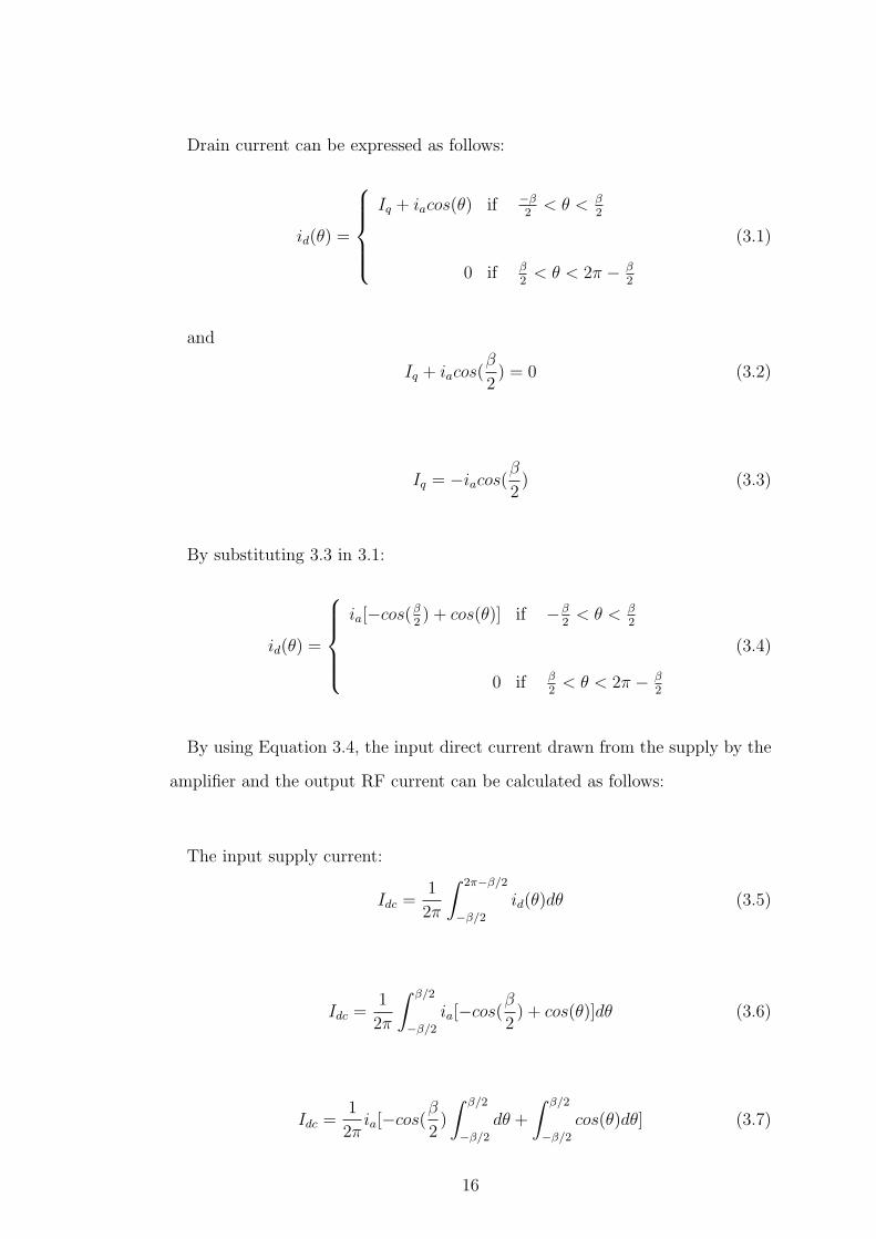
Drain current can be expressed as follows:
id(θ) =
Iq + iacos(θ) if −β
2< θ < β
2
0 if β2< θ < 2π − β
2
(3.1)
and
Iq + iacos(β
2) = 0 (3.2)
Iq = −iacos(β
2) (3.3)
By substituting 3.3 in 3.1:
id(θ) =
ia[−cos(β
2) + cos(θ)] if −β
2< θ < β
2
0 if β2< θ < 2π − β
2
(3.4)
By using Equation 3.4, the input direct current drawn from the supply by the
amplifier and the output RF current can be calculated as follows:
The input supply current:
Idc =1
2π
∫ 2π−β/2
−β/2
id(θ)dθ (3.5)
Idc =1
2π
∫ β/2
−β/2
ia[−cos(β
2) + cos(θ)]dθ (3.6)
Idc =1
2πia[−cos(
β
2)
∫ β/2
−β/2
dθ +
∫ β/2
−β/2
cos(θ)dθ] (3.7)
16

Idc =1
2πia[−cos(
β
2)β + 2sin(
β
2)] (3.8)
Output RF current:
IRF =1
π
∫ 2π−β/2
−β/2
id(θ)cos(θ)dθ (3.9)
IRF =1
π
∫ β/2
−β/2
ia[−cos(β
2) + cos(θ)]cos(θ)dθ (3.10)
IRF =1
πia[−cos(
β
2)
∫ β/2
−β/2
cos(θ)dθ +
∫ β/2
−β/2
cos2(θ)dθ] (3.11)
IRF =1
πia[
−sin(β)
2+
β
2] (3.12)
IRF =ia2π
(β − sin(β)) (3.13)
The input DC power and output power are found as follows:
The input DC power:
PDCin = Vdc × Idc (3.14)
PDCin = Vdc ×ia2π
[−cos(β
2)β + 2sin(
β
2)] (3.15)
17

The output RF Power:
PRFout =va√2× IRF√
2(3.16)
PRFout =vaia(β − sin(β))
4π(3.17)
Hence, the efficiency is found:
η =PRFout
PDCin
(3.18)
η =va(β − sin(β))
2Vdc(2sin(β2)− βcos(β
2))
(3.19)
When the maximum input power is applied, the maximum output voltage
swing is obtained, va = Vdc
This point is the maximum achievable efficiency:
ηmax =β − sin(β)
2(2sin(β2)− βcos(β
2))
(3.20)
Figure 3.2 shows the maximum achievable efficiency with respect to conduc-
tion angle.
18

Figure 3.2: Maximum Achievable Efficiency vs. Conduction Angle
3.2 Efficiency Enhancement and Dynamic Load
From Equation 3.19 it is seen that efficiency can be increased at low input
power levels by increasing the output voltage swing while keeping the power
gain constant. In other words, va will reach to the maximum value (Vdc), before
the maximum input power is applied. This can be realized by increasing the
load impedance while the output power is constant. For instance, one amplifier
that is matched to R ohms in the first case, the same amplifier is matched to 2R
ohms in the second case. If the output power is same for these two cases, it is
obvious that the output voltage swing is larger in the second case than the first
case, so the efficiency is higher.[6]
This concept works well up to the point where maximum output voltage swing
is obtained. In the second case this occurs much earlier than in the first case.
In other words, the amplifier saturates more quickly and hence the maximum
available output cannot be obtained.
19

The solution is to use a dynamic load, its value will change according to the
input power. At low input levels, a high value load impedance will be used so
that the efficiency is high up to the point where the maximum output voltage
swing is obtained. Then, the load impedance decreases that keeps output voltage
swing and the efficiency high and results in an increase of output power. This
can be implemented by using an additional voltage source in series with the load
as seen in Figure 3.3. [6] [3]
Figure 3.3: Usage of Additional Voltage Source
In Figure 3.3, the load impedance value is equal to twice of the optimum load
impedance. In the low power region, the generator is off, its output impedance is
zero so that amplifier is matched by an impedance of 2Ropt (optimum impedance)
so the efficiency is high. In the high power region, the generator starts to deliver
power hence the voltage of node between the generator and the load increases.
This concludes that the effective load impedance seen by the amplifier decreases,
hence, the amplifier can deliver more power without any decrease at the drain
voltage. When the power delivered by the generator becomes equal to the power
delivered by the amplifier, the effective impedance becomes equal to Ropt and the
amplifier returns back to the optimum case, delivering the maximum available
power. On the second branch, the generator also delivers the same power thus,
20

the total output power delivered by the system becomes twice that of the single
amplifier. (However, because the input power is split into two branches at the
input there is no gain increase in overall system. But the maximum available
power and consequently P1dB increase.)
The generator can be realized by using a second amplifier. The output of an
RF amplifier is a high impedance when it is cut-off. So, the amplifier cannot
directly be connected to the load as done with the generator which has zero out-
put impedance. This problem can be solved simply by using impedance inverting
network as shown in Figure 3.4.
Figure 3.4: Usage of Second Amplifier
In the configuration depicted in Figure 3.4 the load is in series with the am-
plifiers and this is not very practical for implementation. Instead of the series
connection, a shunt connection is used. This configuration is shown in Figure
3.5. When the maximum input power is applied both amplifiers should be ter-
minated by the Ropt to be able to deliver maximum available output power. For
this reason the system is terminated by a load with an impedance of half of the
21

optimum load (Ropt/2). An impedance inverting network is used at the output
of the main amplifier so that in the low power region the low load impedance
value is converted to a high value. More specifically, a circuit is designed such
that Ropt/2 is matched to 2Ropt whereas Ropt is matched to Ropt again.[6]
Figure 3.5: Doherty Configuration with Shunt Load
3.3 Doherty Amplifier Configuration
A general explanation and the final output configuration is given in the Chapter
3.2 and in Figure 3.5. A few additions of circuit blocks should be done to finalize
the Doherty Amplifier configuration.
For the rest of the thesis the main amplifier and the second amplifier are called
as ”Carrier Amplifier” and ”Peaking Amplifier”, respectively, to be consistent
with the general terminology.
22

Overall Doherty Power Amplifier system is given in Figure 3.6.
3.3.1 Carrier Amplifier
The carrier amplifier operates in the linear region at low power levels and
saturates (nonlinear region) at high power levels. Class-AB or Class-B amplifiers
are used as carrier amplifiers. The efficiency at low power region is determined
by the efficiency of this amplifier. [5]
3.3.2 Peaking Amplifier
The peaking amplifier does not conduct at low power levels and its transistor
is cut-off. At high power levels or at the peaks of the modulated input signal it
turns on and compensates the nonlinearity of the carrier amplifier, hence a linear
amplified power is obtained. This amplifier should be biased as Class-C to meet
the required specifications both at low power and at high power region. Also, it
is very important that the output of this amplifier should have a high impedance
value when it is in cut-off, otherwise the power delivered by the carrier amplifier
flows through this branch. [5]
3.3.3 Matching Circuits
Both amplifiers have their own input and output matching circuits. Amplifiers
can be matched to predefined load impedances that is used in Doherty Config-
uration. Since, 50Ω system is used, amplifiers are matched to 50Ω individually.
As a result, they can be implemented and tested independently.
23
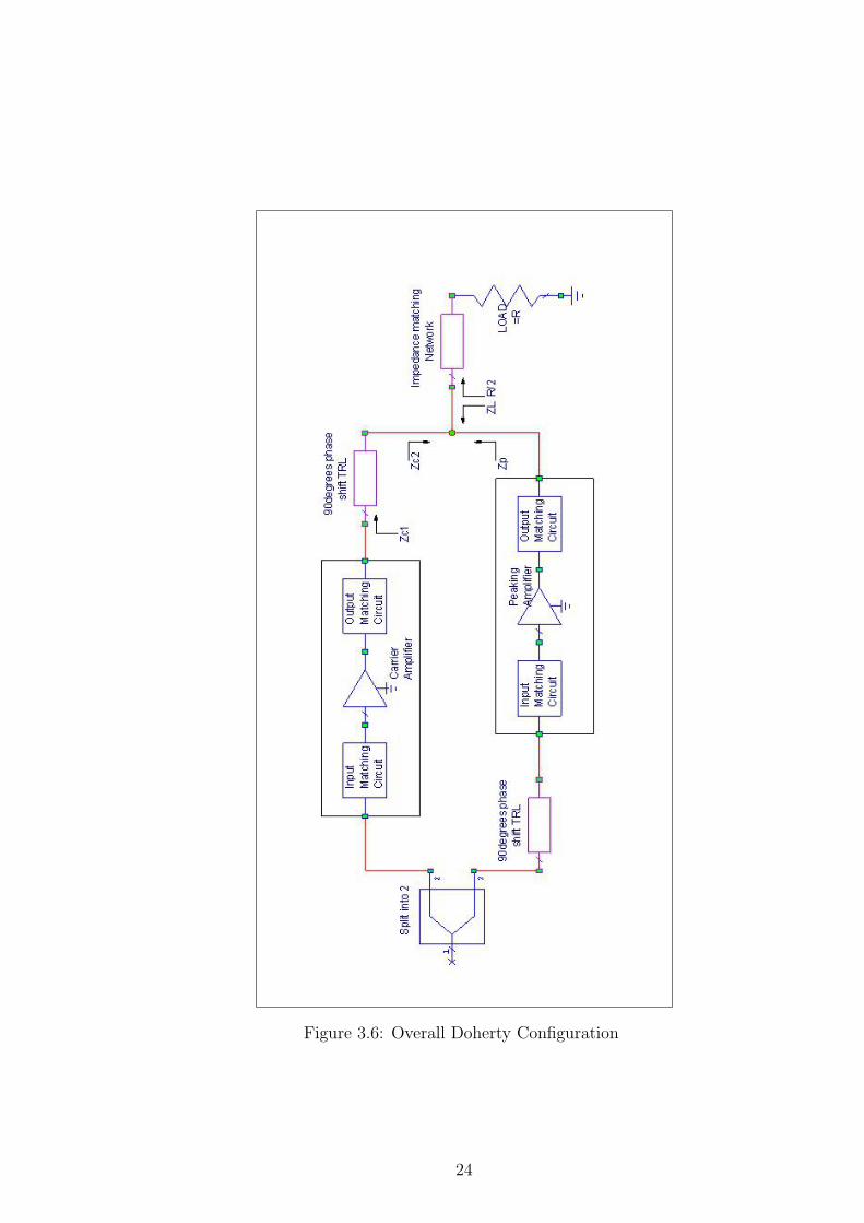
Figure 3.6: Overall Doherty Configuration
24

In the thesis, the amplifiers are matched to 50Ω : Zc1 = Zp = 50Ω when two
amplifiers are operating at full power.
Hence the load impedance of 25Ω is used: ZL = R/2 = 25Ω. [6] [3]
3.3.4 Impedance Inverting Network
This part of the circuit has two important roles as mention in Chapter 3.2:
• Matching R/2 to 2R
• Matching R to R (do not change anything)
This circuit can be designed in a few ways, by using Π-match or T-match cir-
cuits with capacitors and inductors. However the simplest and the most practical
way is to use a 90 transmission line with a characteristic impedance of ZTRL1.
[6]
By using the notations given in Figure 3.6 the characteristic impedance can
be calculated as follows:
ZTRL1 =√Zc1Zc2 (3.21)
• At low power region:
ZTRL1 =
√R
22R (3.22)
ZTRL1 = R (3.23)
25

• At high power region:
ZTRL1 =√RR = R (3.24)
3.3.5 Phase Compensation Network
The impedance inverting network at the output of the carrier amplifier causes
a 90 phase difference between two branches. When operating at full power, two
amplifiers are out-of phase. This problem can be solved by adding an additional
90 phase shift at the input of peaking amplifier as seen in Figure 3.6. Since the
input of amplifier is 50Ω, the characteristic impedance of this transmission line
should be 50Ω.
3.3.6 Impedance Matching Network
Doherty system output is matched to R/2 = 25Ω whereas R = 50Ω system is
used. Therefore, a matching network is required at the output. This network is
simply a λ/4 transmission line. [3] [5]
The characteristic impedance of this transmission line is calculated as follows:
ZTRL2 =
√R
2R (3.25)
ZTRL2 =R√2
(3.26)
ZTRL2 = 35.35Ω (3.27)
26

3.3.7 Efficiency of Doherty Amplifier
The theoretical efficiency of Doherty Amplifier can be calculated by making
some assumptions:
• Ideal amplifiers are used, the peaking amplifier does not consume any power
at low power region up to the transition point.
• The carrier amplifier is biased as Class-B and the peaking amplifier operates
like Class-B amplifier after transition point.
• The output voltage swing of carrier amplifier increases linearly up to the
transition point and thereafter it remains constant and is equal to the
supply voltage.
• The output current of peaking amplifier increasing linearly after the tran-
sition point. At maximum input point, output currents of two amplifiers
become equal. (Increasing rate of peaking amplifier’s current is twice the
increasing rate of carrier amplifier’s current)
In the following calculations [11] the transition point is considered as it occurs
at the point where the input voltage is half of the maximum available input
voltage. At this point va =Vdc
2.
The output power of Doherty Amplifier:
PRFout dh =va
2(R2)
(3.28)
27

The input supply current of Doherty Amplifier:
Idc dh =
va
π(R2)
if 0 < va <Vdc
2
3va−Vdc
π(R2)
if Vdc
2< va < Vdc
(3.29)
The input DC power:
PDCin dh =
vaVdc
π(R2)
if 0 < va <Vdc
2
3vaVdc−V 2dc
π(R2)
if Vdc
2< va < Vdc
(3.30)
The overall efficiency:
ηdh =
π2
vaVdc
if 0 < va <Vdc
2
π2× [ v2a
3Vdcva−V 2dc] if Vdc
2< va < Vdc
(3.31)
In this equation, both parts of equation gives the same result for va = Vdc
2
which shows the continuity of the efficiency curve.
From 3.19 the efficiency of Class-B amplifier can be found by substituting
β = π:
ηCl−B =π
4× va
Vdc
(3.32)
These two efficiency functions are plotted on the same graph in Figure 3.7.
28

Figure 3.7: Theoretical Efficiencies of Doherty Amplifier and Class-B Amplifier
The efficiency of Doherty amplifier for low power region is very similar to
the efficiency of Class-B amplifier, except it reaches to the maximum value at
transition point as a result of using twice of the optimum load value. A decrease
occurs at the Doherty efficiency because the full voltage swing does not occur at
the output of peaking amplifier. At full power point, both peaking and carrier
amplifiers operates as Class-B amplifiers, hence the same efficiency is achieved
again.
3.4 Practical Approaches
Some practical approaches used in the design of a Doherty power amplifier can
summarized as follows:
• The phase compensation transmission line at the input of peaking amplifier
and the power divider circuit can be combined. One 3dB quadrature hy-
brid coupler can be used at the input by connecting the lagging pin to the
29

peaking amplifier. This configuration can be seen in the Figure 3.8. [3] [12]
Figure 3.8: Final Configuration for Doherty Amplifier
• The impedance inverting network (transmission line) at the output of the
carrier amplifier can be used as a part of the output matching circuit.
In other words, output matching circuit can be designed such that when
carrier amplifier is terminated by R/2 its output voltage is twice the output
voltage when it is terminated by R. In Figure 3.8, this transmission line
is not shown explicitly, indeed it is embedded into the output matching
circuit. [12] [13]
• The output of peaking amplifier should be high impedance when it is in
cut-off. Also to make impedance seen by the carrier amplifier change from
R/2 to R carrier amplifier’s output impedance should change from high
impedance to 50Ω. However because of the output matching circuit of the
peaking amplifier sometimes the desired case is not obtained. Usage of
an additional transmission line at the output as seen in Figure 3.8 can
solve this problem easily. At high power region amplifier is matched to
50Ω hence the transmission line’s characteristic impedance should be 50Ω
in order not to corrupt the matching. At low power region, if the output
30

impedance is low enough than this transmission line can easily convert it
to a high impedance. If the output impedance is very close to 50Ω than
this technique does not work. The choice of amplifier and the design of
output matching circuit should be done by considering this. [14] [15] [16]
• An extra transmission line can be added to the output of the carrier am-
plifier for proper phase matching and for creating an extra flexibility point
for output matching. [14] [15]
• At the outputs of amplifiers shunt capacitors are very useful in terms of
the slight modification of phase matching and output impedance in the
practical implementation. [14] [15]
31

Chapter 4
DESIGN OF AMPLIFIER AND
SIMULATION RESULTS
In the thesis, MRFG35010AR1 transistors from Freescale are used for sim-
ulation and implementation. This is a GaAs PHEMT with 10W P1dB. All
simulations are done by using AWR Design Environment.
In the implementation Rogers-4003 substrate with thickness of 20mil, and
copper on both sides is used. The simulations are done by using the specifications
of this substrate.
4.1 Determining the Bias Points
First, I-V curves are drawn to determine the biasing points. Indeed, the exact
biasing points are stated precisely at the simulation of Doherty configuration.
These curves are used to learn the general characteristic of the amplifier with
respect to the gate bias voltage.
32

The circuit depicted in Figure 4.1 is used and the corresponding I-V traces
are given in Figure 4.2 and Figure 4.3. MRFG35010AR1 is used with a drain
voltage of 12V.
Figure 4.1: The Circuit that is Used to Plot I-V Traces
When the amplifier is biased as Class-A, the quiescent current is half of linear
maximum drain current swing which is about 3A. From Figure 4.2 it is observed
that, the quiescent current of 1.5A is obtained when the gate-source voltage is
approximately -0.3V. When the gate bias is set to -1V, nearly zero quiescent
drain current is observed from Figure 4.3, which tells us that this point is Class-
B biasing point. By adjusting the gate voltage between these two values, the
amplifier operates as Class-AB, and below -1V, it operates as Class-C.
In the design, the carrier amplifier is biased as Class-AB and -0.7V gate voltage
is chosen as the starting point. The peaking Amplifier is biased as Class-C and
the gate voltage should be well below -1V, which will be determined in the design
of Doherty configuration.
33

Figure 4.2: I-V Traces for Different Gate Voltages
Figure 4.3: The Zoomed Version of I-V Traces for Different Gate Voltages
34

4.2 Carrier Amplifier Design
The carrier amplifier design involves the input and output matching circuits,
the biasing circuitry and the stability analysis.
4.2.1 Input Matching Circuit Design
The circuit that is used to find out the input and output impedances of the
amplifier is given in Figure 4.4. 12V drain voltage and -0.7V gate voltage are
applied by using bias-tees, so an ideal case is assumed.
Figure 4.4: Basic Amplifier Circuit to Find the Input Matching
35

The conjugate values of input and output impedances’ S-parameters (S11 and
S22) are plotted in Figure 4.5.
Figure 4.5: Input and Output Impedances of the Amplifier
As observed from the figure, the input impedance changes as the gate voltage
changes. The input power level, the output matching network and the biasing
circuit cause slight differences in the impedance, for this reason, the input match-
ing circuit is desired to have a wide bandwidth. The designed circuit and the
corresponding S-parameter result (S43) with the input impedance of amplifier
(S11) are given in Figure 4.6 and Figure 4.7, respectively.
36

Figure 4.6: Input Matching Circuit
Figure 4.7: Response of Input Matching Circuit and Input Impedance of Ampli-fier
37

4.2.2 Output Matching Circuit Design
The output matching points are determined by a load-pull analysis. The cir-
cuit that is used in load-pull analysis is given in Figure 4.8. The input matching
circuit is added, bias-tees are used again and at the output LTUNER element is
used. This element matches the circuit to specified points and stores the results.
Figure 4.8: Carrier Amplifier Circuit with Input Matching Used in Load-PullAnalysis
A load-pull analysis is done for different input power levels. The results are
shown in Figure 4.9, Figure 4.10, Figure 4.11 and Figure 4.12 for 20dBm,
25dBm, 30dBm and 35dBm input power, respectively.
38

Figure 4.9: Load-Pull Contour Graph for 20dBm Input Power
Figure 4.10: Load-Pull Contour Graph for 25dBm Input Power
Figure 4.11: Load-Pull Contour Graph for 30dBm Input Power
39

Figure 4.12: Load-Pull Contour Graph for 35dBm Input Power
As expected the output impedances for maximum gain and maximum output
power are different. The amplifier should be matched to approximately (12 −
10j)Ω and to (15− 20j)Ω at low and high input power levels, respectively.
The carrier amplifier should be matched to 100Ω if the impedance inverting
network is considered as a separate element (not as a part of the carrier amplifier)
where the impedance at the combining point is 25Ω for the low power levels. In
the design of carrier amplifier, the impedance inverting network is considered as
a part of the output matching circuit as shown is Figure 3.8. So, the output
matching circuit inherently transforms 25Ω to the wanted output impedance for
the low power levels. On the other hand, for high power levels, 50Ω is matched
to the wanted output impedance.The output matching circuit is given in Figure
4.13 and the corresponding results are shown at Figure 4.14.
40

Figure 4.13: Output Matching Circuits for Both 25Ω and 50Ω termination
The output matching network is simulated both with terminations of 25Ω and
50Ω and S11 is matched to the maximum gain and S33 is matched to the maxi-
mum output power as seen from Figure 4.14.
The resultant circuit, after the addition of output matching circuit is given in
Figure 4.15 and its gain characteristic for 25Ω and 50Ω termination impedances
are shown in Figure 4.16. The gain is higher when terminated with 25Ω how-
ever it saturates earlier. On the other hand, when terminated with 50Ω although
the gain is lower the P1dB point is much higher. The composition of these two
characteristics is desired by the addition of peaking amplifier.
41

Figure 4.14: Load-Pull Contour Graphs for 20dBm and 35dBm Input Powersand Responses of Matching Circuits
Figure 4.15: Carrier Amplifier Circuit with the Addition of Output MatchingCircuit
42

Figure 4.16: Gain of Carrier Amplifier with Both 25Ω and 50Ω Terminations
4.2.3 Final Circuit with Biasing Circuits and Stability
Analysis
Ideal capacitors are used up to this point in the design. Model files of capacitors
from ”Murata” are also replaced with the ideal capacitors. The resulting circuit
diagram is shown in Figure 4.17. The capacitor values are slightly changed to
be closer to the ideal case, however some degradation is observed at the overall
characteristics.
Biasing circuits are added instead of the bias-tees. Shunt capacitors are used
at the voltage supply nodes to make this point RF ground. 90 transmission line
(one fourth of the wavelength on the substrate) is used both to invert this RF
ground to open circuit at the base of amplifier. The width of these transmission
lines are chosen sufficiently small, at gate biasing 10mil, at drain biasing 20mil.
This property enables them to behave as RF chokes.
43
After the replacement of the bias-tees with these circuits, as depicted in Figure
4.17, no significant change in overall characteristic is observed.
There were stability problems both at low frequencies and at high frequencies.
• A series resistor with a parallel capacitor at the RF line is used to overcome
the stability issue at low frequencies. The series resistor decreases the gain
in the whole band whereas the capacitor shorts the resistor at high frequen-
cies which recovers some loss in gain. The value of resistance is chosen as
small as possible, a 10Ω resistor is used. The capacitor should have high
impedance at low frequencies and low impedance at high frequencies.
• Series resistance is used at gate bias line to maintain stability at high
frequencies. This resistance should be as small as possible to save the gain
and 25Ω is used. After the insertion of this resistance some gain degradation
is also observed.
The corresponding stability plots, K and B values, are given in Figure 4.18.
No stability problem is observed from 100MHz up to 10GHz.
4.2.4 Results of Carrier Amplifier
The large signal S parameters at different input power levels are given in
Figure 4.19, Figure 4.20 for 25Ω load impedance and in Figure 4.21, Figure
4.22, Figure 4.23 for 50Ω load impedance. The input return loss changes as a
result of change of the input impedance with respect to input power. In all cases,
44

Figure 4.17: Final Carrier Amplifier Circuit with the Addition of Biasing Cir-cuits, Stabilization Elements and Real Capacity Models
45

Figure 4.18: K and B parameters for Carrier Amplifier
S11 is less than -10dB for a bandwidth of 200MHz (4.65 GHz to 4.85 GHz), this
is satisfied by wide-band matching of input. Since the matching is done by using
small signal S-parameters, best matching is observed in Figure 4.21 when 20dB
input power is applied and 50Ω load impedance is used. The gain (S21) also
decreases at high power levels due to the nonlinearity of amplifier, whereas in all
cases the gain is very flat in the band of 4.75GHz±100MHz. The bandwidth of
Doherty configuration is not limited by the single amplifier design. Actually, it
is limited by the 90 phase shifts and the phase compensation networks. When
the two branches have different phase characteristics, amplifiers are out-of-phase
and gain starts to decrease.
46

Figure 4.19: Large Signal S11 and S21 of Carrier Amplifier with 20dBm InputPower and 25Ω Termination
Figure 4.20: Large Signal S11 and S21 of Carrier Amplifier with 30dBm InputPower and 25Ω Termination
47

Figure 4.21: Large Signal S11 and S21 of Carrier Amplifier with 20dBm InputPower and 50Ω Termination
Figure 4.22: Large Signal S11 and S21 of Carrier Amplifier with 30dBm InputPower and 50Ω Termination
48

Figure 4.23: Large Signal S11 and S21 of Carrier Amplifier with 34dBm InputPower and 50Ω Termination
The carrier amplifier’s gain response is given in Figure 4.24 for both 25Ω
and 50Ω, which is very similar to the gain characteristics given in Figure 4.16.
Moreover, same observations are also valid except there is a gain degradation
due to the stabilization circuits and usage of model files for capacitors.
In ideal case, when 25Ω termination is used the output power should be 3dB
higher (twice much power) than the output power when 50Ω termination is used.
This is required to fulfill the loss from input power divider (hybrid coupler is used)
at low power levels. At full power by the contribution of peaking amplifier the
gain also increases 3dB at the output. (Indeed because of the loss at the input
overall gain remains same.) Furthermore, in order to have a flat gain response,
carrier amplifier’s gain should 3dB higher at low power levels. [6] [17]
49

Figure 4.24: Final Gain of Carrier Amplifier with Both 25Ω and 50Ω Termina-tions
In practical cases, the acquisition of 3dB more power is very difficult, however
it should be as much as possible. In the carrier amplifier power gain decreased
considerably by the addition of stabilization circuits. The difference between
gain characteristics of 50Ω and 25Ω terminations is about 0.4dB.
Power added efficiency and DC efficiency are shown in Figure 4.25 and Figure
4.26 respectively. At low input power levels, the efficiency is higher because of
the slight increase of gain when 25Ω load is used, and efficiency decreases at high
power levels because of the quick saturation.
50

Figure 4.25: PAE of Carrier Amplifier with Both 25Ω and 50Ω Terminations
Figure 4.26: Drain Efficiency of Carrier Amplifier with Both 25Ω and 50Ω Ter-minations
51

4.3 Peaking Amplifier Design
Since the input matching circuit is designed independent of input power level
and gate bias point, the same circuit is used at the input of the peaking amplifier.
Also the same biasing and stabilization circuits are used. Hence, in the peaking
amplifier design, basically the output matching circuit is focused on.
4.3.1 Output Matching Circuit Design
The same design procedure is followed: After the design of input matching,
output matching circuit is designed. Thereafter, the biasing and stabilization
circuits and real capacitor models are added.
The circuit given in Figure 4.8 is used for the load-pull analysis only with the
exception that gate voltage is reduced below -1V, hence the amplifier operates
as Class-C amplifier.
Figure 4.27 and Figure 4.28 show the load-pull contours for the gain of the
amplifier for 30dBm and 35dBm input powers respectively. A low power analysis
is not performed, because the amplifier operates only at high power levels. In
these graphs a gate voltage of -1.5V is used, the amplifier operates below the
Class-B point. The output matching point is also indicated (with legend name
”LoadCircuit”).
52
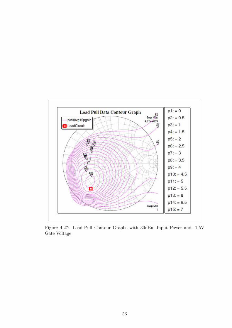
Figure 4.27: Load-Pull Contour Graphs with 30dBm Input Power and -1.5VGate Voltage
53

Figure 4.28: Load-Pull Contour Graphs with 35dBm Input Power and -1.5VGate Voltage
54

Figure 4.29 shows the same data for 34dBm input power and a gate voltage
of -2.3V, (biased as Class-C). The output impedances for these two gate biases
are very close to each other.
Figure 4.29: Load-Pull Contour Graphs with 34dBm Input Power and -2.3VGate Voltage
Simulations with different gate bias levels are performed also and very similar
results are obtained. Since the output impedance is very similar, the gate bias
can be easily changed with no significant effect on the output impedance.
Output matching circuit is given in Figure 4.30:
55

Figure 4.30: Output Matching Circuit Of Peaking Amplifier
4.3.2 Results of Peaking Amplifier
The final design of the peaking amplifier is completed with the addition of
peripheral elements. The large signal S parameters for gate voltage -1.5V are
presented in Figure 4.31, Figure 4.32 and Figure 4.33 for input power levels
20dBm, 30dBm and 34dBm, respectively.
Figure 4.31: Large Signal S11 and S21 of Peaking Amplifier with 20dBm InputPower and -1.5V Gate Voltage
56

Figure 4.32: Large Signal S11 and S21 of Peaking Amplifier with 30dBm InputPower and -1.5V Gate Voltage
57

Figure 4.33: Large Signal S11 and S21 of Peaking Amplifier with 34dBm InputPower and -1.5V Gate Voltage
When 20dBm input power is applied, the gain is very small as observed from
Figure 4.31. This indicates that the amplifier is very near the turn-on point.
The input return loss is not very well defined. Similar to the input impedance,
the output impedance is also not very well defined and in the region of transition.
This point is the most problematic region since the amplifier is neither in cut-off
nor have a linear flat gain response. The impedance seen by the carrier amplifier
starts to change.
At input power levels below this value, the amplifier is off and does not produce
any gain, whereas above this level the peaking amplifier operates more linearly
58

and its output approaches to the output of carrier amplifier and modulates the
output impedance.
The flat gain response and well defined S11 characteristics are observed in Fig-
ure 4.32. In addition to the similar observations, there is some gain compression
in Figure 4.33.
Figure 4.34, Figure 4.35 and Figure 4.36 show large signal S11 and S21 values
for input power levels 30dBm, 34dBm and 36dBm respectively when -2.9V gate
voltage is used.
Similar results are observed with these two different gate voltages. The differ-
ence is that, more input power is required to turn on the amplifier with smaller
gate bias. The critical power level which the amplifier starts to turn on is about
30dBm and a maximum gain is obtained at about 34dBm. It saturates at a
higher input power.
Figure 4.37 shows the gain characteristic of the peaking amplifier for different
gate bias points. As the gate bias point increases, the input power which amplifier
starts to operate linearly decreases and P1dB point increases with the cost of
efficiency.
59

Figure 4.34: Large Signal S11 and S21 of Peaking Amplifier with 30dBm InputPower and -2.9V Gate Voltage
Figure 4.35: Large Signal S11 and S21 of Peaking Amplifier with 34dBm InputPower and -2.9V Gate Voltage
60

Figure 4.36: Large Signal S11 and S21 of Peaking Amplifier with 36dBm InputPower and -2.9V Gate Voltage
Figure 4.37: Gain Characteristic of the Peaking Amplifier for Different Gate BiasPoints
61

DC efficiency and power added efficiency of peaking amplifier for a gate bias
of -1.5V is given in Figure 4.38 and for a gate bias -2.9V is given in Figure 4.39.
Figure 4.38: PAE and Drain Efficiency for Peaking Amplifier with -1.5V GateVoltage
4.4 Combining the Amplifiers
4.4.1 Design of Impedance Matching Network (Com-
biner) at the Output
From Section 3.3.6 this network is explained as only a quarter wavelength
transmission line and from Equation 3.27 its characteristic impedance is found
as 35.35Ω. The width and length of the transmission line are calculated as 76mil
62
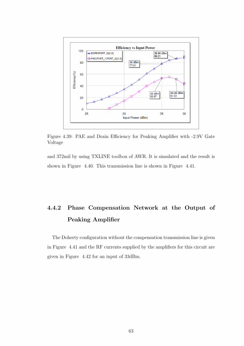
Figure 4.39: PAE and Drain Efficiency for Peaking Amplifier with -2.9V GateVoltage
and 372mil by using TXLINE toolbox of AWR. It is simulated and the result is
shown in Figure 4.40. This transmission line is shown in Figure 4.41.
4.4.2 Phase Compensation Network at the Output of
Peaking Amplifier
The Doherty configuration without the compensation transmission line is given
in Figure 4.41 and the RF currents supplied by the amplifiers for this circuit are
given in Figure 4.42 for an input of 33dBm.
63

Figure 4.40: Input Impedance of Combiner
Figure 4.41: Doherty Amplifier Configuration without the Phase CompensationNetwork
64

Figure 4.42: RF Currents at the Output of Each Amplifier and at the CombinedBranch of Doherty Amplifier without Compensation Network
The current waveforms are out-of-phase and have a phase difference of about
122ps. 4.75GHz signal’s period is 210,5ps and the wavelength is 1490mil on the
substrate used. Hence the length of this transmission line is calculated:
length of compensation line = 122210.5
× 1490 = 863mil
The exact value is found as 985mil by simulations. The compensation line
should have a characteristic impedance of 50Ω, so width is 44mil.
In the given diagrams, the coupler at the input is the only element used as
ideal with no insertion loss which is not very realistic approach. The insertion
loss is set as 0.25dB to be more realistic. The final Doherty configuration by the
addition of compensation line is given in Figure 4.43.
65

RF current waveforms with the compensation line are also shown in Figure
4.44.
Figure 4.43: Final Doherty Amplifier with the Addition of Compensation Line
Figure 4.44: RF Currents at the Output of Each Amplifier and at the CombinedBranch of Doherty Amplifier with Compensation Transmission Line
Also as explained in Chapter 4.6 there is no gain degradation at low power
levels due to the addition of peaking amplifier. This proves that the compensation
66

line also matches the output of peaking amplifier to high impedance when it is
off, while not affecting the output matching at high power levels.
4.5 Balanced Amplifier Design
Doherty amplifier is designed by using two amplifiers, thus it is not so fair
to compare with a single Class-AB amplifier. Instead the comparison should be
done with another configuration that uses two amplifiers. For this purpose a
balanced power amplifier is designed using same amplifiers.
In the design of balanced amplifier, two carrier amplifiers are used since they
are matched to maximum output power for 50Ω system. Amplifiers are biased
to the same point with carrier amplifiers to have similar linearity characteristics.
At the input and output two hybrid couplers are used for power dividing and
combining purposes. Insertion losses of the couplers are also set to 0.25dB to
obtain more reliable results.
The block diagram for the balanced power amplifier configuration is given in
Figure 4.45.
Figure 4.45: Balanced Amplifier Block Diagram
67

4.6 Results of Doherty Amplifier, Balanced
Amplifier and Single Carrier Amplifier
-0.7V is used as the gate voltage of carrier amplifier in all three configurations.
The gate voltage of peaking amplifier is Doherty configuration is determined
after analyzing the results of Doherty Configuration. Power gain and efficiency
of Doherty Amplifier for different gate biases are given in Figure 4.46, Figure
4.47 and Figure 4.48. The gate voltages used for these graphs are −2V , −2.5V
and −3.3V respectively. The power gain characteristic of Doherty Amplifier for
-2.9V gate voltage is given in Figure 4.49 and Figure 4.50 together with gain
characteristics of other configurations.
First of all from Figure 4.24 the gain of the carrier amplifier is about 7.75dB
at low power levels when terminated by 25Ω. In Doherty configuration this gain
decreases by an amount of 3.25dB at the coupler (coupling and insertion loss)
and as a result 4.5dB gain should be observed. The Doherty Amplifier gain at
low power levels is observed as 4.69dB from all five graphs mentioned. This
proves that all the RF power supplied by the carrier amplifier is delivered to the
load, peaking amplifier does not affect the output impedance seen by the carrier
amplifier which is 25Ω. (Indeed there is an additional 0.11dB gain which shows
that carrier amplifier is matched to a better point which increases the gain a
little bit.)
The gain characteristic of Doherty amplifier is highly dependent on the turn-on
point of peaking amplifier. It turns-on at earlier power levels if the bias point is
set to a high point and by the gain contribution from peaking amplifier overall
gain characteristic becomes a wavy shape as seen in Figure 4.46 and Figure
68

Figure 4.46: Power Gain and Drain Efficiency vs. Output Power with -2V GateVoltage for Peaking Amplifier
4.47. If the bias level is set to a low level the peaking amplifier does not turn-on
properly even at high power levels as seen in Figure 4.48. In these cases the
best P1dB and the efficiency is not achieved. The optimum gate bias point is
found as -2.9V where the gain has a very smooth shape (Figure 4.49 and Figure
4.50) and maximum P1dB and efficiency is achieved at this point. Also in all
cases there is a dip in the gain plot. This is the point where peaking amplifier
starts to turn on. At this point efficiency of Doherty amplifier also diverge from
the efficiency of the single carrier amplifier. [18]
In Figure 4.26 when the amplifier is terminated with 25Ω the drain efficiency is
observed 33.07 % for an input power of 26dBm (which gives an output of 33dBm).
This drain efficiency is more than the drain efficiency of amplifier terminated by
50Ω. Same situation can be observed in Figure 4.48 where the efficiency is 33.19
% at output power 33dBm for the Doherty amplifier and it is higher than the
carrier amplifier. When gate voltage is adjusted as -3.3V the peaking amplifier
does not consume any power so the efficiency is higher at this power level. As the
69

gate bias increases, the efficiency at this power level decrease since the amplifier
starts to consume power although it does not turn on exactly.
Figure 4.47: Gain and Drain Efficiency vs. Output Power with -2.5V GateVoltage for Peaking Amplifier
1dB compression points of Doherty amplifier, balanced amplifier and carrier
amplifier are found from Figure 4.49 and summarized in Table-P1dB with im-
provement with respect to the P1dB of carrier amplifier.
Table 4.1: P1dB for Three Different ConfigurationsConfiguration P1dB(dBm) Improvement(dB)
Carrier 40 —Balanced 43 2.7Doherty 43 3
70

Figure 4.48: Power Gain and Drain Efficiency vs. Output Power with -3.3V GateVoltage for Peaking Amplifier
Figure 4.49: Power Gain of Carrier, Doherty and Balanced Amplifiers vs. OutputPower with -2.9V Gate Voltage for Peaking Amplifier Used at Doherty Amplifier
71

Figure 4.50: Power Gain of Carrier, Doherty and Balanced Amplifiers vs. InputPower with -2.9V Gate Voltage for Peaking Amplifier Used at Doherty Amplifier
The efficiencies are investigated next, the corresponding graphs and compar-
ison tables are presented. PAE vs. Output Power, Drain Efficiency vs Output
Power, PAE vs Back-off and Drain Efficiency vs Back-off graphs are given in
Figure 4.51, Figure 4.52, Figure 4.53 and Figure 4.54 respectively.
Doherty amplifier’s PAE is very close to carrier amplifier’s PAE at low power
levels for same output power. After peaking amplifier turns on, the PAE starts to
become closer to balanced amplifier’s PAE. The same observations are also done
for drain efficiency characteristic. However for a fair comparison the efficiencies
vs. back-off graphs should be investigated. Low efficiency of Doherty amplifier at
same output power is reasonable, because the P1dB point of Doherty Amplifier
is higher than the other configurations.
The early saturation and low P1dB for the carrier amplifier is also observed in
Figure 4.51 and Figure 4.52.
72
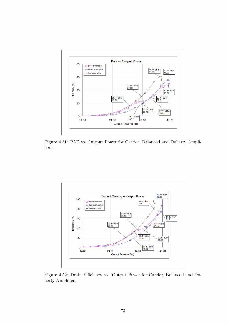
Figure 4.51: PAE vs. Output Power for Carrier, Balanced and Doherty Ampli-fiers
Figure 4.52: Drain Efficiency vs. Output Power for Carrier, Balanced and Do-herty Amplifiers
73

Figure 4.53: PAE vs. Back-off for Carrier, Balanced and Doherty Amplifiers
The PAE of Doherty Amplifier is lower than the other amplifiers at high power
levels. The reason for this situation is its low gain. However we observe that
at low power levels Doherty configuration works well and the Doherty amplifier
becomes more efficient in terms of PAE. Table-PAE shows the PAEs of three
configurations for different back-off levels.
Since the output power of the single amplifier is very low, the comparison
is done between the Doherty Amplifier and Balanced Amplifier and ”improve-
ment” row indicates the improvement of Doherty Configuration according to the
Balanced.
The PAE of Doherty amplifier is 5.7 % lower at 0dB back-off level due to the
low gain. At 6dB back-off point PAEs are equal and at 10dB back-off point there
is an improvement about 7.2 %.
74

Table 4.2: Power Added Efficiency (%)Configuration 0dBBack − off 6dBBack − off 10dBBack − off
Carrier 61 31 17Balanced 56 28 15Doherty 50 28 22Improvement -5.7 0.13 7.2
Figure 4.54: Drain Efficiency vs. Back-off for Carrier, Balanced and DohertyAmplifiers
The drain efficiency of Doherty amplifier is higher for all back-off values. The
results are summarized in Table 4.3.
Table 4.3: Drain Efficiency (%)Configuration 0dBBack − off 6dBBack − off 10dBBack − off
Carrier 78.9 37.32 20.18Balanced 74.3 35.13 18.97Doherty 86.85 42.45 33.38Improvement 12.55 7.32 14.41
At 0dB and 10dB back-off points Doherty amplifier is highly efficient, 12.55
% and 14.41 % respectively. However at 6dB back-off point (output power of
75

37.44dBm) efficiency improvement decreases to 7.32 %, because the dip at the
gain occurs at this point.
76

Chapter 5
IMPLEMENTATION AND
RESULTS
In the implementation we used a Rogers-4003 substrate with thickness of 20mil,
and copper on both sides.
We found that the transistor’s model is not accurate at 4.75GHz and good
results could not be obtained at this frequency. For this reason, the implemented
circuit is redesigned at 2GHz. Some modification are done on the circuit board
and good results are obtained. The implemented single amplifier is tested at
2GHz and the results are compared.
The carrier amplifier in the Doherty configuration is biased as Class-AB and
simulations indicate that the quiescent drain current is about 400mA. For this
purpose, the gate voltage of carrier amplifier is adjusted to about -0.8V. The
peaking amplifier is biased as Class-C by adjusting the gate voltage below -1V.
In the experiments, the best performance is achieved when the gate voltage is
set to -1.3V. This value is also not the same as the value found from simulation.
77

In order not to effect the gain of the Doherty configuration at low power levels,
the output impedance of the peaking amplifier seen by the carrier amplifier (at
the combining point) should be high. The measured impedance is shown in
Figure 5.1 and it is about 200Ω. It is far from being an open circuit, however
the gain is not affected significantly by this impedance.
Figure 5.1: Output Impedance of Peaking Amplifier at the Combining Point, themarker 1 shows the value of the impedance
At high power levels, the two amplifiers should work in-phase, in other words
the delays of the branches should be very close. The phase measurement results
of the carrier amplifier and peaking amplifier are given in Figure 5.2 and Figure
5.3.
78

Figure 5.2: Phase Measurement of Carrier Amplifier
Figure 5.3: Phase Measurement of Peaking Amplifier
79

The difference of the phase values at high input power levels is very small,
indicating that the amplifiers operate in-phase.
In Figure 5.4 and Figure 5.5 the gain of the Doherty Amplifier is shown
for an input power of 18.4dBm and input power of 31.1dBm, respectively. The
curves at the bottom of the figures show the gain of the driver amplifier and the
difference between two curves at 2.0175GHz shows the gain of Doherty Amplifier.
Figure 5.4: Measured gain of the Doherty Amplifier at Low Power Levels
The gain in Figure 5.5 shows the P1dB point of the Doherty Amplifier where
output power is 39.2dBm.
80

Figure 5.5: Measured gain of the Doherty Amplifier at P1dB point
The gain of the single amplifier at P1dB point is given in Figure 5.6 which
gives 37dBm output power
The gain of both amplifiers are shown in Figure 5.7. As seen from figure the
there is a 2dB increase at P1dB point.
In figures 5.8 and 5.9 the power added efficiency and the drain efficiency of
amplifiers are given with respect to output power.
81

Figure 5.6: Measured gain of the Single Amplifier at P1dB point
26 28 30 32 34 36 38 406
7
8
9
10
11
12
X: 28.6Y: 9.2
Gai
n (d
B)
Output Power (dBm)
Gain vs Output Power
X: 39.1Y: 8.201
X: 30.05Y: 11.1 X: 36.67
Y: 10.1
Doherty AmplifierSingle Amplifier
Figure 5.7: Measured gain of the Single and the Doherty amplifiers
82

26 28 30 32 34 36 38 4010
20
30
40
50
60
70
X: 36.6Y: 55.12
Pow
er A
dded
Effi
cien
cy (
%)
Output Power (dBm)
PAE vs Output Power X: 39.1Y: 67.22
X: 33.1Y: 31.09
X: 30.66Y: 22.44
Doherty AmplifierSingle Amplifier
Figure 5.8: Power added efficiency of the Single and the Doherty amplifiers
26 28 30 32 34 36 38 4010
20
30
40
50
60
70
80
X: 39.1Y: 79.23
Dra
in E
ffici
ency
(%
)
Output Power (dBm)
Drain Efficiency vs Output Power
X: 33.1Y: 35.57
X: 36.68Y: 66.24
X: 30.68Y: 24.46
Doherty AmplifierSingle Amplifier
Figure 5.9: Drain efficiency of the Single and the Doherty amplifiers
83
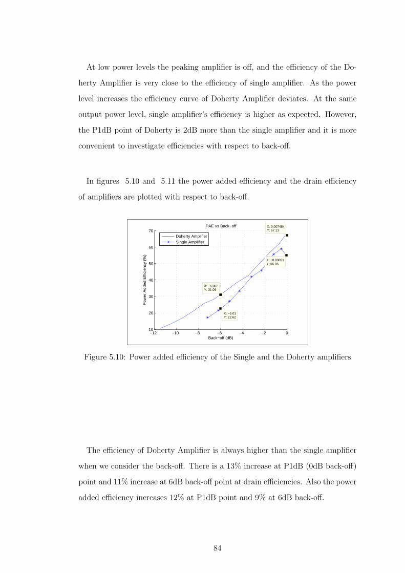
At low power levels the peaking amplifier is off, and the efficiency of the Do-
herty Amplifier is very close to the efficiency of single amplifier. As the power
level increases the efficiency curve of Doherty Amplifier deviates. At the same
output power level, single amplifier’s efficiency is higher as expected. However,
the P1dB point of Doherty is 2dB more than the single amplifier and it is more
convenient to investigate efficiencies with respect to back-off.
In figures 5.10 and 5.11 the power added efficiency and the drain efficiency
of amplifiers are plotted with respect to back-off.
−12 −10 −8 −6 −4 −2 010
20
30
40
50
60
70
X: 0.007484Y: 67.13
Pow
er A
dded
Effi
cien
cy (
%)
Back−off (dB)
PAE vs Back−off
X: −0.03051Y: 55.05
X: −6.01Y: 22.62
X: −6.002Y: 31.09
Doherty AmplifierSingle Amplifier
Figure 5.10: Power added efficiency of the Single and the Doherty amplifiers
The efficiency of Doherty Amplifier is always higher than the single amplifier
when we consider the back-off. There is a 13% increase at P1dB (0dB back-off)
point and 11% increase at 6dB back-off point at drain efficiencies. Also the power
added efficiency increases 12% at P1dB point and 9% at 6dB back-off.
84

−12 −10 −8 −6 −4 −2 010
20
30
40
50
60
70
80
Dra
in E
ffici
ency
(%
)
Back−off (dB)
Drain Efficiency vs Back−off
X: 0.008954Y: 79.28
X: −6Y: 24.59
X: −0.001224Y: 66.36
X: −6.009Y: 35.49
Doherty AmplifierSingle Amplifier
Figure 5.11: Drain efficiency of the Single and the Doherty amplifiers
85

Chapter 6
CONCLUSIONS
The objective of the thesis is to investigate and explain the Doherty amplifier
configuration, the principles and the practical approaches.
Firstly, the amplifier classes and balanced amplifiers are reviewed focusing on
the efficiency of the amplifiers. The theory of Doherty configuration is investi-
gated by stating also the practical approaches. A Doherty amplifier operating at
4.75GHz is designed by using 10W GaAs pHEMT transistor (MRFG35010AR1)
by using both the theoretical and practical approaches. The design procedure
includes the design of the carrier amplifier, the peaking amplifier, the power com-
biner and the phase compensation line at the output of the peaking amplifier.
The carrier amplifier is matched to maximum gain point for 25Ω termination and
the maximum available output power point for 50Ω termination. The Peaking
amplifier is matched to the maximum available output power. The length of
phase compensation line is found from the phase difference between the drain
currents of carrier and peaking amplifiers.
One balanced amplifier is also designed by using the same transistors for the
purpose of comparing the performances of Doherty amplifier.
86

The implementation of Doherty amplifier is also done following the same steps.
However, because of the inaccuracy of the amplifier model the results are not as
expected. An implementation is done at 2GHz and the measurement results are
compared with a single amplifier which operates as Class-AB.
In the simulations, P1dB point of Doherty amplifier is found as 0.27dB more
than the balanced amplifier and 3dB more than the carrier amplifier. The effi-
ciencies are basically compared at back-off power levels. Efficiency comparisons
are done with the balanced amplifier. PAE improvement is achieved only at
10dB back-off point which is 7.23%. At high power levels the loss in gain dom-
inated the efficiency improvement and no PAE is obtained. On the other hand,
12.55% drain efficiency improvement is achieved at the peak power. Also, 7.32%
and 14.41% improvements are achieved at 6dB and 10dB back-off points, respec-
tively.
The measurement results show that Doherty Amplifer has a higher P1dB point
than the single amplifier. The efficiency of single amplifier is higher at same
output power levels, since the gain of the Doherty Amplifier is lower than the
single amplifier. However, when the efficiency at P1dB point or at back-off
regions are considered the advantage of Doherty Amplifier is demonstrated. We
obtained a 13% increase at P1dB (0dB back-off) point and a 11% increase at
6dB back-off point in drain efficiencies.
87

Bibliography
[1] R. Ludwig and P. Bretchko, RF Circuit Design. Prentice Hall, 2000.
[2] Q. Hammi, J. Kim, I. Kim, S. Boumaiza, S. Hong, B. Kim, and F. Ghan-
nouchi, “RF power amplifiers for emerging wireless communications: Single
branch vs. multi-branch architectures,” in Electrical and Computer Engi-
neering, 2006. CCECE ’06. Canadian Conference, pp. 598–601, 2006.
[3] S. C. Cripps, Advanced Techniques in RF Power Amplifier Design. Artech
House, 2002.
[4] A. Z. Markos and G. Kompa, “High power Doherty amplifier design for
UMTS application.”.
[5] F. H.Raab, P. Asbeck, S. Cripps, P. Kenington, Z. B. Popovic, N. Pothecary,
J. F. Sevic, and N. O. Sokal, “Power amplifiers and transmitters for RF
and microwave,” IEEE Transactions on Microwave Theory and Techniques,
vol. 50, 2002.
[6] W. H. Doherty, “A new high efficiency power amplifier for modulated
waves,” Proceedings of the Institute of Radio Engineers, vol. 24, no. 9, 1936.
[7] D. A. Neamen, Electronic Circuit Analysis and Design. McGraw-Hill Inter-
national Edition, second ed., 2001.
[8] S. C. Cripps, RF Power Amplifiers for Wireless Communications. Artech
House, second ed., 2006.
88

[9] L. Max, “Balanced transistors: A new option for RF design,” Microwaves,
1977.
[10] J. Shumaker, R. Basset, and A. Skuratov, “High power GaAs FET am-
plifiers: Push- pull versus balanced configurations,” Wireless Symposium,
2001.
[11] F. H. Raab, “Efficiency of Doherty RF power-amplifier systems,” IEEE
Transactions on Broadcasting, vol. 33, 1987.
[12] K. F. Brand, “The experimental design and characterisation of Doherty
power amplifiers,” Master’s thesis, Stellenbosch University, 2006.
[13] V. Viswanathan, “Efficiency enhancement of base station power amplifiers
using Doherty technique,” Master’s thesis, Virginia Polytechnic Institute
and State University, 2004.
[14] K.-J. Cho, J.-H. Kim, and S. P. Stapleton, “A highly efficient Doherty
feedforward linear power amplifier for W-CDMA base-station applications,”
IEEE Transactions on Microwave Theory and Techniques, vol. 53, no. 1,
2005.
[15] K.-J. Cho, I.-H. Hwang, W.-J. Kim, J.-H. Kim, and S. P. Stapleton, “Linear-
ity optimization of a high power Doherty amplifier,”Microwave and Wireless
Components Letters, IEEE, vol. 15, 2005.
[16] J. Kim, J. Cha, I. Kim, S. Y. Noh, C. S. Park, and B. Kim, “Advanced
design methods of Doherty amplifier for wide bandwidth, high efficiency
base station power amplifiers,” in Microwave Conference, 2005 European,
p. 4 pp., 2005.
[17] J. Cha, J. Kim, B. Kim, J. S. Lee, and S. H. Kim, “Highly efficient power am-
plifier for CDMA base stations using Doherty configuration,” in Microwave
Symposium Digest, 2004 IEEE MTT-S International, pp. 533–536, 2004.
89

[18] K. J. Smith, K. W. Eccleston, P. T.Gough, and S. I.Mann, “The effect of
FET soft turn-on on a Doherty amplifier,” Microwave and Optical Technol-
ogy Letters, vol. 50, 2008.
90
![Design of a High-Efficiency Broadband Asymmetric Doherty … · 2019. 5. 18. · The Doherty power amplifier [1] (DPA) can maintain a high efficiency within a certain power back-off](https://img.pdfslide.net/doc/110x75/61489f552918e2056c22ceb7/design-of-a-high-eifciency-broadband-asymmetric-doherty-2019-5-18-the-doherty.jpg)