Embed Size (px)
Citation preview

DEVELOPMENT OF A HIGH-EFFICIENCY POWER AMPLIFIER
FOR ENVELOPE TRACKING APPLICATIONS
A thesis submitted to Cardiff University
In candidature for the degree of
Doctor of Philosophy
By
Zulhazmi A. Mokhti, M.Sc.
Centre for High Frequency Engineering
School of Engineering
Cardiff University
United Kingdom
September 2016

i
DECLARATION
This work has not previously been accepted in substance for any degree and
is not concurrently submitted in candidature for any degree.
Signed ………………………………………………..…(candidate)
Date …………………
STATEMENT 1
This thesis is being submitted in partial fulfilment of the requirements for the
degree of PhD.
Signed …………………….………………………….. (candidate)
Date …………………
STATEMENT 2
This thesis is the result of my own independent work/investigation, except
where otherwise stated. Other sources are acknowledged by explicit
references.
Signed ……………………...…………………………(candidate)
Date …………………
STATEMENT 3
I hereby give consent for my thesis, if accepted, to be available for
photocopying and for inter-library loan, and for the title and summary to be
made available to outside organisations.
Signed ……………………...……………………..…(candidate)
Date …………………
ZulhazmiMokhti
ZulhazmiMokhti
ZulhazmiMokhti
ZulhazmiMokhti
30 Sep 2016
30 Sep 2016
30 Sep 2016
30 Sep 2016

ii
ABSTRACT
Complex and spectrally efficient modulation schemes present a power-efficiency challenge to base station power amplifiers due to the time-varying envelope and high peak-to-average power ratios involved. The envelope tracking architecture is one way to address this issue, where an envelope amplifier provides a dynamic, modulated supply to the power amplifier to reduce power consumption.
While most research into envelope tracking focuses on the envelope amplifier, this work focuses on optimising the power amplifier design for envelope tracking using the waveform engineering approach. It studies the behaviour of a highly-efficient power amplifier mode of operation (class-F) using a relatively low-cost high voltage laterally diffused metal oxide semiconductor (HVLDMOS) technology in an envelope tracking environment. A systematic design process is formulated based on identifying the optimum amplifier load and the envelope shaping function, and then applied in the development of an actual class-F power amplifier.
The fabricated power amplifier is integrated into an envelope tracking system and is able to produce one of the highest recorded efficiencies compared to current state-of-the-art envelope tracking amplifiers, which are mostly based on Gallium Nitride technology. The limitation of this design is its linearity performance, and the efficiency-linearity trade-off is analysed in detail in this work.
The use of continuous mode power amplifiers in envelope tracking is also explored for high-bandwidth operation. The limitation of such a technique is posed by the device nonlinear output capacitance, and this is analysed through the use of a novel characterisation approach called voltage-pull, which is derived from an active load-pull system but uses voltage waveforms as the target instead of loads.
This method is also used to investigate the possibility of exploiting the device nonlinear output capacitance as a 2nd harmonic injection source to improve power amplifier efficiency, as predicted in a novel mathematical analysis presented in this work.

iii
KEY CONTRIBUTIONS
Contribution 1: Waveform-based characterisation of class-F and continuous
class-F power amplifier modes in an envelope tracking environment.
Contribution 2: A waveform-based trade-off analysis between efficiency and
linearity for different power amplifier modes in an envelope tracking
architecture.
Contribution 3: Formulation of a design flow using waveform engineering to
optimise the design of an RF power amplifier for envelope tracking
applications.
Contribution 4: Design and fabrication of a high voltage LDMOS class-F
power amplifier using the formulated design flow, and its integration into a real
envelope tracking system.
Contribution 5: A novel mathematical analysis of the effect of the nonlinear
device output capacitance, or the varactor effect, on continuous mode power
amplifiers.
Contribution 6: A novel characterisation method for continuous mode power
amplifiers called the voltage-pull method, which exposes the varactor effect
that is hidden with conventional load-pull methods.
Contribution 7: Mathematical, simulation, and experimental work to
investigate the use of device nonlinear output capacitance or varactor as a 2nd
harmonic injection source to improve amplifier efficiency.

iv
ACKNOWLEDGEMENTS
All praise to God for without His enabling grace I would never be able to complete this research on my own capacity. Peace and salutations to the beloved Messenger who had set the example of benefiting others with one’s knowledge and actions.
I am blessed to be surrounded by wonderful and supporting people throughout this PhD journey. My heartfelt gratitude goes to my wife who has been very supportive of me and our 3 children while also working on her own PhD, not to mention finishing hers well ahead of mine. I am thankful to my children who were pulled into this journey together and always reminding their parents how enjoyable this family ‘time-off’ together. I also am grateful for the support and encouragement from my loving parents and in-laws, as well as my brothers and sisters.
I have 2 amazing supervisors who have both contributed tremendously to my PhD journey. Professor Paul Tasker has provided the steer that I need while at the same time giving me freedom to find my own direction. Dr Jonathan Lees spent a considerable amount of his time to accommodate this research work from the beginning, providing hands-on advice, as well as administrative matters related to the Opera Net 2 project and others. I have learned a great deal from the regular discussions I had with them. Being a student in Cardiff, I also had the privilege of learning directly from Distinguished Professor Steve Cripps, whose lectures I really enjoy listening to ever since my MSc program.
This research is part of the Opera-Net 2 project and I am honoured to have the opportunity to work with Dr Cedric Cassan from Freescale/NXP who has been supportive with industry-related advice as well as the materials needed for this research. Similarly, I have the rest of the Opera-Net 2 partners to thank to, for their contributions towards this research, in particular Jerome David from Arelis for the envelope tracking system integration, Mika Lasanen and Sandrine Boumard from VTT, Timo Galkin and Hans Otto Scheck from Nokia, Marc Aubree and Patrick Zimmermann from Orange, and Vlad Grigore from Efore. I have a lot of respect for this team and enjoyed the time spent together in face-to-face meetings and review sessions.
No research is possible without funding. I am indebted to Cardiff University for the Presidential Scholarship, Freescale Toulouse (now NXP), as well as Yayasan Daya Diri Malaysia for the financial assistance they have provided me with.
During my 4 years in Cardiff I got to know many friends and colleagues who provided assistance along the way: Rich Rogers was always there when I needed to fabricate a circuit, Tim Canning opened up my understanding in Class-F power amplifiers, Minghao Koh and Lawrence Ogboi provided hands-on help with the measurement system, David Loescher was my go-to person for complex programming issues, Rob Smith was our mentor, Vince Carrubba, Yusri Jalil & family, and many others.
To the current PhD students I wish you all the best in your research and enjoy the wonderful Cardiff experience!
v
LIST OF PUBLICATIONS
First author:
1. Z. Mokhti, P. Tasker, and J. Lees, "Correlation analysis between a VNA-
based passive load pull system and an oscilloscope-based active load pull
system: A case study," in Microwave Measurement Conference (ARFTG),
2014 83rd ARFTG, 2014, pp. 1-4.
2. Z. A. Mokhti, J. Lees, P. J. Tasker, and C. Cassan, "Investigating the
linearity versus efficiency trade-off of different power amplifier modes in an
envelope tracking architecture," in Microwave Conference (EuMC), 2015
European, 2015, pp. 1208-1211.
3. Z. A. Mokhti, P. J. Tasker, and J. Lees, "Using waveform engineering to
optimize class-F power amplifier performance in an envelope tracking
architecture," in Microwave Conference (EuMC), 2014 44th European,
2014, pp. 1301-1304.
4. Z. A. Mokhti, P. J. Tasker, and J. Lees, "Analyzing the improvement in
efficiency through the integration of class-F power amplifiers compared to
class-AB in an envelope tracking architecture," in Teletraffic Congress
(ITC), 2014 26th International, 2014, pp. 1-4.
5. Z. A. Mokhti, P. J. Tasker, and J. Lees, "Analyzing device behaviour at the
current generator plane of an envelope tracking power amplifier in a high
efficiency mode," in Automated RF & Microwave Measurement Society
(ARMMS) Conference 2014.
Co-authored:
6. A. Imtiaz, Z. A. Mokhti, J. Cuenca, and J. Lees, "An integrated inverse-F
power amplifier design approach for heating applications in a microwave
resonant cavity," in 2014 Asia-Pacific Microwave Conference, 2014, pp.
756-758.
7. M. Lasanen, M. Aubree, C. Cassan, A. Conte, J. David, S. E. Elayoubi, et
al., "Environmental friendly mobile radio networks: Approaches of the
European OPERA-Net 2 project," in Telecommunications (ICT), 2013 20th
International Conference on, 2013, pp. 1-5.
8. F. L. Ogboi, P. Tasker, Z. Mokhti, J. Lees, J. Benedikt, S. Bensmida, et al.,
"Sensitivity of AM/AM linearizer to AM/PM distortion in devices," in
Microwave Measurement Conference (ARFTG), 2014 83rd ARFTG, 2014,
pp. 1-4.

vi
LIST OF ACRONYMS
2D-EM Two dimension electromagnetic simulation
2G Second generation mobile communication system
3G Third generation mobile communication systems
4G Fourth generation mobile communication systems
AC Alternating current
ACPR Adjacent channel power ratio
ADS Advanced Design System
AM Amplitude modulation
APT Average power tracking
BB Baseband
CDS Drain-to-source capacitance
CGD Gate-to-drain capacitance
CO2 Carbon dioxide
CW Continuous wave
DA Doherty amplifier
DAC Digital-to-analogue converter
DC Direct current
DC-IV Direct-current current-to-voltage ratio
DE Drain efficiency
DPD Digital pre-distortion
DUT Device under test
EA Envelope amplifier
EER Envelope Elimination and Restoration
ET Envelope Tracking
FET Field effect transistor
FFT Fast Fourier Transform
FPGA Field-programmable gate array
GaN Gallium Nitride
GOPT Optimum gain
HBT Heterojunction bipolar transistor
HEMT High electron mobility transistor
HFET Heterostructure field effect transistor

vii
I In-phase
IF Intermediate frequency
IGEN Current generator
IM3 Third order intermodulation
IM5 Fifth order intermodulation
IMAX Maximum current
LDMOS Laterally diffused metal oxide semiconductor
LTE Long Term Evolution
MLIN Microstrip element
MMIC Monolithic microwave integrated circuit
NVNA Nonlinear vector network analyser
OBO Output back-off
OPEX Operating expense
PA Power amplifier
PAE Power added efficiency
PAPR Peak-to-average power ratio
pHEMT Pseudomorphic high electron mobility transistor
PIN Input power
PM Phase modulation
PRBS Pseudo-random bit sequence
Q Quadrature
RF Radio frequency
RFPA Radio frequency power amplifier
RON On-resistance
ROPT Optimum resistance
TLIN Transmission line element
TRL Thru Reflect Line
VDS Drain-to-source voltage
VIN Input voltage
VMAX Maximum voltage
VNA Vector network analyser
W-CDMA Wideband Code Division Multiple Access
viii
TABLE OF CONTENT
CHAPTER 1 .................................................................................................... 1
INTRODUCTION ............................................................................................. 1
1.1 Research Motivation .......................................................................... 1
1.2 Research Objectives .......................................................................... 4
1.3 Thesis Organization ........................................................................... 5
1.4 References ........................................................................................ 7
CHAPTER 2 .................................................................................................... 9
OVERVIEW OF ENVELOPE TRACKING AND OTHER HIGH-EFFICIENCY
POWER AMPLIFIERS..................................................................................... 9
2.1 Introduction ........................................................................................ 9
2.2 High Efficiency Power Amplifiers: Modes and Architectures ............. 10
2.3 Research Areas in Envelope Tracking Power Amplifiers .................. 19
2.4 State-of-the-Art Envelope Tracking PA’s .......................................... 25
2.5 Conclusions & New Research Opportunities .................................... 26
2.6 References ...................................................................................... 27
CHAPTER 3 .................................................................................................. 35
CLASS-F POWER AMPLIFIER BEHAVIOUR IN A VARIABLE DRAIN BIAS
SETTING ....................................................................................................... 35
3.1 Introduction ...................................................................................... 35
3.2 Measurement System and Device under Test .................................. 36
3.3 Maintaining Class-F in a Variable Drain Setting ............................... 38
3.4 Analysing the Linearity vs. Efficiency Trade-Off for Different PA Modes in an ET Architecture........................................................................ 44
3.5 Relating the ET Linearity Improvement Results with Previous Baseband Injection Work ................................................................. 52
3.6 Conclusions ..................................................................................... 58
3.7 References ...................................................................................... 60
ix
CHAPTER 4 .................................................................................................. 62
USING WAVEFORM ENGINEERING TO OPTIMISE PA DESIGN FOR
ENVELOPE TRACKING APPLICATIONS .................................................... 62
4.1 Introduction ...................................................................................... 62
4.2 Formulating the Design Flow of a Class-F PA for an ET Application 63
4.3 Designing the PA ............................................................................. 69
4.4 Conclusions ..................................................................................... 77
4.5 References ...................................................................................... 79
CHAPTER 5 .................................................................................................. 80
ENVELOPE TRACKING SYSTEM LEVEL INTEGRATION AND TESTING . 80
5.1 Introduction ...................................................................................... 80
5.2 Initial PA Standalone Performance Test ........................................... 80
5.3 Integrating the Class-F PA into the ET System ................................ 82
5.4 ET Measurement Results & Discussions .......................................... 87
5.5 Verifying the Measured ET Test Results in Simulation ..................... 92
5.6 Conclusions ..................................................................................... 98
5.7 References ...................................................................................... 99
CHAPTER 6 ................................................................................................ 101
UTILISING CONTINUOUS MODE POWER AMPLIFIERS IN ENVELOPE
TRACKING & THE VARACTOR EFFECT .................................................. 101
6.1 Introduction .................................................................................... 101
6.2 Formulation of the Continuous Class-BJ and Class-F .................... 103
6.3 Investigating the Continuous Class-F Mode of an LDMOS Device at a Single Drain Bias ........................................................................... 105
6.4 Investigating the Continuous Class-F Mode of an LDMOS Device at a Variable Drain Setting .................................................................... 109
6.5 A Novel Mathematical Analysis of the Varactor Effect on Continuous Mode Power Amplifiers .................................................................. 114
6.6 Conclusions ................................................................................... 127
6.7 References .................................................................................... 127

x
CHAPTER 7 ................................................................................................ 129
EXPOSING THE VARACTOR EFFECT IN MEASUREMENT: THE
VOLTAGE-PULL METHOD ........................................................................ 129
7.1 Introduction .................................................................................... 129
7.2 Load-Pull Approach vs. Voltage-Pull Approach .............................. 130
7.3 Simulation of the Varactor Effect on Continuous Class-BJ Power Amplifier Using Voltage-Pull ........................................................... 132
7.4 Experimental Setup to Analyse the Varactor Effect on Continuous Class-BJ Using Voltage-Pull .......................................................... 137
7.5 Voltage-Pull Measurement Results & Discussions ......................... 142
7.6 Analysing the Lossy Varactor ......................................................... 150
7.7 Conclusions ................................................................................... 153
7.8 References .................................................................................... 154
CHAPTER 8 ................................................................................................ 155
CONCLUSIONS & FUTURE WORK ........................................................... 155
8.1 Conclusions ................................................................................... 155
8.2 Future Work ................................................................................... 158
8.3 References .................................................................................... 161
APPENDIX A ............................................................................................... 163
Measurement Setup ................................................................................. 163
APPENDIX B ............................................................................................... 172
Simulation Data for the Design Method Formulation ................................ 172
APPENDIX C ............................................................................................... 176
Continuous Mode Power Amplifier Theory ............................................... 176
APPENDIX D ............................................................................................... 181
Voltage-Pull Simulation Method ............................................................... 181
APPENDIX E ............................................................................................... 183
Calculating the Lossy Varactor ................................................................. 183
Chapter 1 Introduction
1
Chapter 1 Introduction
1.1 Research Motivation
The mobile communication industry has seen a tremendous growth
over the past decade, where mobile data traffic has grown 4000-fold [1]. In the
first quarter of 2016, there were 7.4 billion mobile subscriptions worldwide with
half of these broadband subscriptions. Video streaming was the biggest
contributor of smartphone mobile traffic at 43% followed by social networking
at 20% [2]. The usage trend of mobile phones has moved towards heavy-data
cases while the number of users keeps increasing at the same time. It is
expected that the number of mobile subscriptions will exceed 26 billion by
2020 [3].
The rapid growth and the demand for wider bandwidth to cater for the
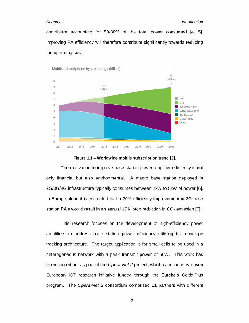
heavy-data traffic shown in Fig. 1.1 have driven the development of more
complex modulation schemes to allow for more users within the limited
available spectrum. However, these spectrally-efficient modulation schemes
present a power-efficiency challenge to the base-station power amplifier (PA)
due to its time-varying envelope and high peak-to-average power ratio (PAPR).
With the introduction of 4th generation mobile communication systems (4G),
rise in energy cost, and the increasing demand in coverage, network operators
are faced with high operating cost (OPEX) where approximately 30% is spent
on base-station energy utilization with the RF power amplifier being the biggest
Chapter 1 Introduction
2
contributor accounting for 50-80% of the total power consumed [4, 5].
Improving PA efficiency will therefore contribute significantly towards reducing
the operating cost.
Figure 1.1 – Worldwide mobile subscription trend [2].
The motivation to improve base station power amplifier efficiency is not
only financial but also environmental. A macro base station deployed in
2G/3G/4G infrastructure typically consumes between 2kW to 5kW of power [6].
In Europe alone it is estimated that a 20% efficiency improvement in 3G base
station PA’s would result in an annual 17 kiloton reduction in CO2 emission [7].
This research focuses on the development of high-efficiency power
amplifiers to address base station power efficiency utilising the envelope
tracking architecture. The target application is for small cells to be used in a
heterogeneous network with a peak transmit power of 50W. This work has
been carried out as part of the Opera-Net 2 project, which is an industry-driven
European ICT research initiative funded through the Eureka’s Celtic-Plus
program. The Opera-Net 2 consortium comprised 11 partners with different
Chapter 1 Introduction
3
specialization areas from within the industry and academia in Europe: Orange
(France), Alcatel Lucent Bell Labs (France), Freescale (France, now NXP),
Nokia (Finland), Thomson Broadcast (France, now Arelis), VTT (Finland),
Efore (Belgium), Cardiff University (UK), Telecom Bretagne (France),
University of Caen (France), and Alpha Technologies (Belgium).
The objective of the Opera Net 2 project is to reduce the environmental
impact of mobile radio networks by analysing and providing an end-to-end
solution from the standpoint of material lifecycle, hybrid energy sites, access
network optimisation, architecture optimisation and hardware design, and
standardization [8]. In terms of the current industry practice in base station
architecture and hardware design, the Doherty PA with digital pre-distortion
(DPD) is the preferred implementation due to its relatively high-efficiency
performance over wide dynamic range whilst delivering high power, coupled
with an absence of a high-power solution from the envelope tracking
architecture [9]. However with the emergence of heterogeneous networks to
address growth in data traffic, smaller cells with lower transmit-power are used
to extend network capacity in dense areas [10, 11]. It is in this type of
application that the envelope tracking PA architecture presents an attractive
high-efficiency solution with its relatively high bandwidth capability, and is the
focus of the Opera-Net 2 project for architecture and hardware design.
Cardiff University’s role in Opera-Net 2 was in the development of a
highly efficient RF PA using Freescale’s next generation high voltage LDMOS
transistors that would be used in an envelope tracking system developed by
Arelis. As such, the Opera-Net 2 project acts as a platform for this PhD

Chapter 1 Introduction
4
research work and provides an industry validation for the designed PA
prototype.
1.2 Research Objectives
There are several objectives outlined in this research towards
developing a high-efficiency mode PA for ET applications using HV-LDMOS
technology. The first objective is to utilize Cardiff University’s waveform
engineering capabilities to understand the effect of variable drain bias on a
high-efficiency mode PA. The output capacitance (CDS) varies nonlinearly with
output voltage and an analysis at the device’s current generator plane is
needed to fully understand the load trajectory in terms of boundary interaction
relative to the IV plane, as a function of ET drain voltage.
The second objective is to use waveform engineering to formulate a
systematic design methodology for a high-efficiency RF PA to be used in an
ET application. This design method will utilize the target load and the
envelope shaping function as design parameters to optimise overall ET
efficiency as well as linearity based on signal PAPR and other design
specifications.
The third objective is to apply the method to design, build, and test a
class-F PA in an industry standard ET system. The ET-integration work is
carried out in collaboration with Arelis, an Opera-Net 2 consortium member
whom with their recent work in ET modulators, provide the capability to adopt a
new, high-efficiency PA into their existing ET system.
The fourth objective is to investigate the use of envelope tracking as a
baseband linearising method. Baseband injection for linearisation is a

Chapter 1 Introduction
5
technique developed at Cardiff University utilising the waveform engineering
system under multi-tone excitations [12]. This method has been proven to
linearise a PA regardless of envelope shape and bandwidth but its effect on
PA efficiency has not been tested.
Finally the fifth objective is to investigate the feasibility of applying
continuous mode PA design in an envelope tracking application, which is an
extension of the first objective. The continuous mode power amplifiers offer a
high efficiency operation over a wider bandwidth but only at its peak power.
The aim is to analyse the effect of nonlinear output capacitance on a
continuous mode PA and how that affects the operation of a continuous mode
amplifier in ET.
Figure 1.2 - Research objectives.
1.3 Thesis Organization
This thesis is organized into eight chapters, summarized as follows:
Chapter 2 provides an overview of high-efficiency power amplifier modes and
architectures. It discusses the challenges faced by the PA design community
in dealing with signals with high PAPR. State-of-the-art power amplifiers of
different architecture are also summarized.
Chapter 3 presents the behaviour of a high-efficiency PA mode in a variable
drain bias setting, which is an environment that can emulate the envelope

Chapter 1 Introduction
6
tracking condition. It investigates the impact of the nonlinear output
capacitance on efficiency when class-F and class-AB Pas are optimised at
different drain bias points. The efficiency and linearity trade-off when using
different envelope shaping functions is also analysed. Through modulated
signal simulations, this chapter also investigates the effectiveness of using ET
as a baseband linearisation method for class-F compared to the previous work
of class-AB.
Chapter 4 describes the process of using waveform engineering to optimise a
class-F PA design for envelope tracking applications based on the
experimental results from Chapter 3. A systematic design method is proposed
and applied in designing an actual class-F PA using an LDMOS device
operating at 900MHz. The design goals, matching network design, and
simulated results are described.
Chapter 5 presents the initial standalone test results of the fabricated class-F
PA followed by the integration of the PA into a full ET system used in the
Opera-Net 2 project. System level test results are then presented, highlighting
the benefits and limitations of using a class-F PA mode in an ET system.
Chapter 6 investigates the integration of a continuous mode PA, which is an
extension of the high-efficiency PA mode to achieve a higher bandwidth, in an
envelope tracking architecture. Starting with a discussion on conventional
continuous mode PA theory, simulated and measured results are then
compared. A novel investigation of the device nonlinear output capacitance
(varactor) effect on continuous mode PAs is presented through mathematical

Chapter 1 Introduction
7
analysis, where one of the theoretical findings points to the possibility of using
the varactor effect for efficiency enhancement under certain load conditions.
Chapter 7 presents an experimental validation to the theory of the varactor
effect on continuous mode PA’s, specifically on class-BJ power amplifiers. A
novel measurement strategy to expose the varactor effect, termed the voltage-
pull, is described. It also experiments with the possibility of exploiting the
varactor as a 2nd harmonic injection source to improve PA efficiency. In doing
so this chapter presents a new design space for continuous mode PA, which is
modified from the conventional design space as a result of the varactor effect.
Chapter 8 summarizes and concludes the overall findings from this research
work and derives future work that can be taken forward.
1.4 References
[1] Cisco Visual Networking Index: Global Mobile Data Traffic Forecast Update 2015-2020. Available: http://www.cisco.com/c/en/us/solutions/collateral/service-provider/visual-networking-index-vni/mobile-white-paper-c11-520862.pdf
[2] Ericsson Mobility Report June 2016. Available: https://www.ericsson.com/res/docs/2016/ericsson-mobility-report-2016.pdf
[3] Ericsson Mobility Report June 2015. Available: https://www.ericsson.com/res/docs/2015/ericsson-mobility-report-june-2015.pdf
[4] L. M. Correia, D. Zeller, O. Blume, D. Ferling, Y. Jading, G. I, et al., "Challenges and enabling technologies for energy aware mobile radio networks," IEEE Communications Magazine, vol. 48, pp. 66-72, 2010.
[5] Z. Wang, Envelope Tracking Power Amplifiers for Wireless Communications: Artech House, 2014.
Chapter 1 Introduction
8
[6] M. Liu, L. Liu, X. Wu, L. Teng, J. Cao, and S. Qin, "A Research on the Telecommunication Base Station Power Consumption Investment Analysis and Optimized Configuration Method for Hybrid Energy Power," in Telecommunications Energy Conference 'Smart Power and Efficiency' (INTELEC), Proceedings of 2013 35th International, 2013, pp. 1-6.
[7] OPERA-Net 2: Optimising Power Efficiency in Mobile Radio Networks 2. Available: http://projects.celticplus.eu/opera-net2/index.html
[8] M. Aubree, D. Marquet, S. Le Masson, H. Louahlia, A. Chehade, J. David, et al., "OPERA-Net 2 Project - An environmental global approach for radio access networks-achievements for off-grid systems," in Telecommunications Energy Conference (INTELEC), 2014 IEEE 36th International, 2014, pp. 1-7.
[9] R. Pengelly, C. Fager, and M. Ozen, "Doherty's Legacy: A History of the Doherty Power Amplifier from 1936 to the Present Day," IEEE Microwave Magazine, vol. 17, pp. 41-58, 2016.
[10] A. Damnjanovic, J. Montojo, Y. Wei, T. Ji, T. Luo, M. Vajapeyam, et al., "A survey on 3GPP heterogeneous networks," IEEE Wireless Communications, vol. 18, pp. 10-21, 2011.
[11] S. Landstrom, A. Furuskar, K. Johansson, L. Falconetti, and F. Kronestedt, "Heterogeneous networks - increasing cellular capacity," Ericsson Review, vol. 1, 2011.
[12] F. L. Ogboi, P. J. Tasker, M. Akmal, J. Lees, J. Benedikt, S. Bensmida, et al., "A LSNA configured to perform baseband engineering for device linearity investigations under modulated excitations," in Microwave Conference (EuMC), 2013 European, 2013, pp. 684-687.
Chapter 2 Envelope Tracking Overview
9
Chapter 2 Overview of Envelope Tracking and Other High-Efficiency Power Amplifiers
2.1 Introduction
Research into power amplifier (PA) efficiency improvement has been
ongoing since the 1930s driven by increasing operating costs associated with
high power (Megawatt) AM broadcast applications due to inefficient power
transmitters and associated cooling requirements [1]. The advent of wireless
mobile communication especially the introduction of the 3rd generation mobile
communication systems (3G) has further increased the need to improve power
amplifier efficiency in order to have longer handsets battery life, lower
electricity cost for network operators, and importantly lower CO2 emission from
mobile networks.
PA’s in typical in typical mobile communications system base stations
are responsible for 50-80% of the total power consumption [2]. From that total
DC power consumed, typically only approximately 30% is converted into useful
transmitted RF signals [3]. The main challenge in producing a high efficiency
power amplifier in such applications is the high peak to average power ratio
(PAPR) of the RF signal, which in some cases is in excess of 10dB [2]. This is
because the PA needs to be efficient not only at peak power but also at

Chapter 2 Envelope Tracking Overview
10
average power levels several dB’s below where the PA would spend most of
its time operating. As the demand for higher bandwidth increases, more
complicated and dynamic modulation schemes are used, driving the signal
PAPR increasingly higher. This puts a lot of pressure on the PA design
community to provide solutions that continually improve PA efficiency and to
react to the advancements in spectrally-efficient schemes, as well as
accommodating the stringent linearity requirements implicit in new wireless
standards.
This chapter provides a brief overview of the envelope tracking power
amplifiers and the current research from literature. It begins by introducing
different high efficiency PA modes that offer high efficiency close to saturation
and at peak envelope power, as well as high-efficiency PA architectures that
offer high efficiency over dynamic range or output back-off. A review of the
state-of-the-art of one of these architectures; envelope tracking (ET) is
presented, covering different aspects of the ET research such as the drain
modulator, use of high-efficiency modes in ET, and linearisation techniques.
Finally this chapter concludes with a discussion of the new research
opportunities based on the latest literature and state-of-the-art review.
2.2 High Efficiency Power Amplifiers: Modes and
Architectures
2.2.1 Addressing Efficiency at Peak Power: PA Modes
The efficiency of a PA, or drain efficiency (DE), is defined as the ratio of
the fundamental output power to the DC supplied power. Another metric that
is often used is power added efficiency (PAE) which takes into account the
gain of the PA, and is defined as the ratio of the difference between output and
Chapter 2 Envelope Tracking Overview
11
input fundamental power over the DC supplied power. For a PA with high
gain, DE and PAE will be similar, but if the PA gain goes below for example
10dB, the DE and PAE difference would be more than 10% [4].
Several techniques have been developed in improving PA efficiency
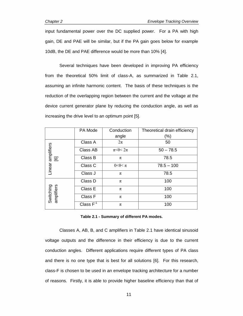
from the theoretical 50% limit of class-A, as summarized in Table 2.1,
assuming an infinite harmonic content. The basis of these techniques is the
reduction of the overlapping region between the current and the voltage at the
device current generator plane by reducing the conduction angle, as well as
increasing the drive level to an optimum point [5].
PA Mode Conduction
angle
Theoretical drain efficiency
(%)
Lin
ea
r a
mp
lifie
rs
[6]
Class A 2π 50
Class AB π<θ< 2π 50 – 78.5
Class B π 78.5
Class C 0<θ< π 78.5 – 100
Class J π 78.5
Sw
itch
ing
am
plif
iers
Class D π 100
Class E π 100
Class F π 100
Class F-1 π 100
Table 2.1 - Summary of different PA modes.
Classes A, AB, B, and C amplifiers in Table 2.1 have identical sinusoid
voltage outputs and the difference in their efficiency is due to the current
conduction angles. Different applications require different types of PA class
and there is no one type that is best for all solutions [6]. For this research,
class-F is chosen to be used in an envelope tracking architecture for a number
of reasons. Firstly, it is able to provide higher baseline efficiency than that of
Chapter 2 Envelope Tracking Overview
12
class-AB, which is typically used in ET power amplifiers. As will be seen in the
next section, there is an opportunity to address this gap in literature for ET
applications.
Secondly class-F is chosen instead of F-1 because of the limitation
presented by the large output capacitance CDS of the LDMOS device used for
this work preventing a proper 2nd harmonic open circuit termination at the
current generator plane with the available active load-pull system. Also as
shown in a load-pull comparison between these 2 modes using LDMOS in [7],
the class-F mode produced 4%-point higher peak drain efficiency compared to
F-1 for the same bias point. This was considered due to the increase in drain
current during the off-state for the class- F-1 mode at high input drive as the
output voltage approaches breakdown. This peak drain efficiency is important
for this work as it determines the highest achievable efficiency for a particular
bias, and the strategy is then to use ET to maintain it over dynamic range
through the use of an ET shaping function. This design strategy is discussed
in more detail in Chapter 4.
Thirdly, even though class-F mode is narrowband in its operation, it can
be built upon to produce a wideband design space through the use of the
continuous class-F mode [8]. In [9] a continuous class-F mode PA has been
realized using a 10W GaN HEMT and a 74% average drain efficiency was
achieved over an octave bandwidth. The topic of extending the bandwidth for
this LDMOS class-F is described in Chapter 6.
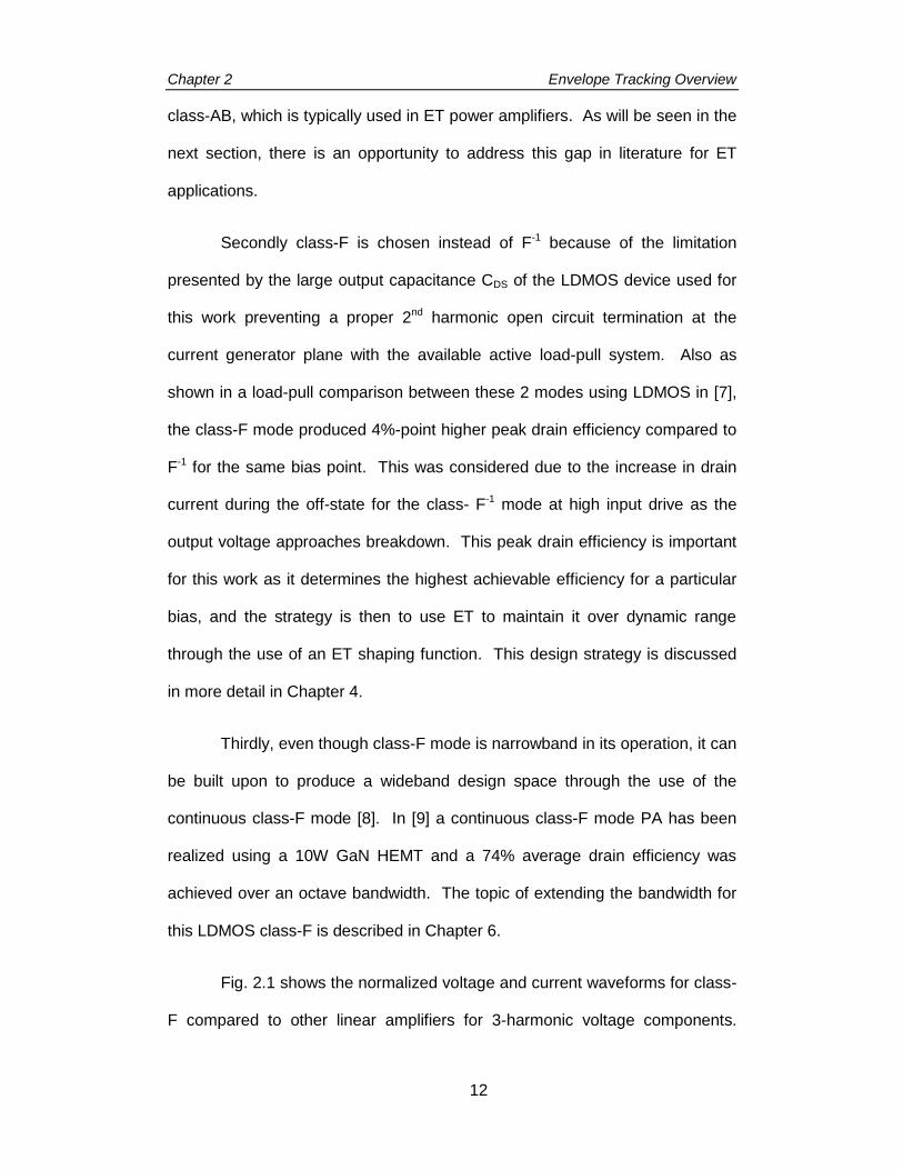
Fig. 2.1 shows the normalized voltage and current waveforms for class-
F compared to other linear amplifiers for 3-harmonic voltage components.
Chapter 2 Envelope Tracking Overview
13
With 3-harmonic voltage components, the theoretical efficiency of class-F
drops to 90.7% [10].
Figure 2.1 - Normalized current and voltage waveforms for class-AB, B, C, F, J.
2.2.2 Addressing Efficiency at Output Back-Off: PA Architectures
While the high-efficiency PA modes described in the previous section
produce promising efficiencies, they are only efficient near peak power when
the device starts to go into compression. However, when the PA operates
below peak power under output back-off (OBO) conditions, the efficiency drops
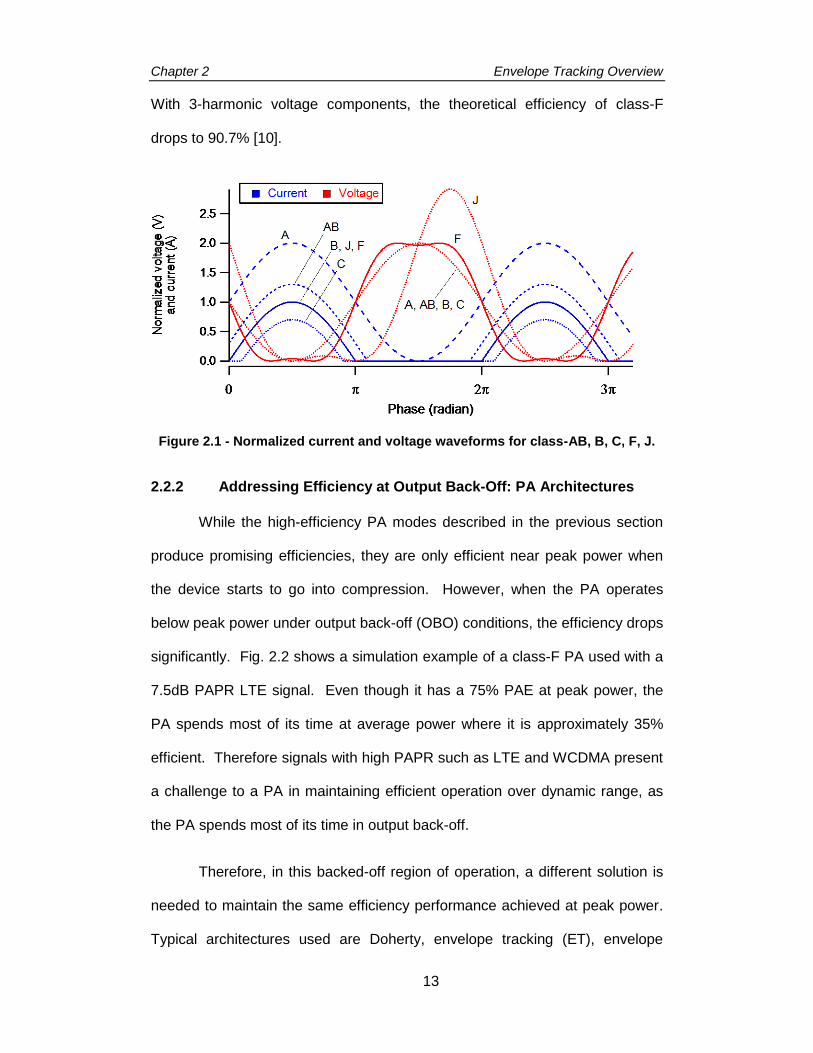
significantly. Fig. 2.2 shows a simulation example of a class-F PA used with a
7.5dB PAPR LTE signal. Even though it has a 75% PAE at peak power, the
PA spends most of its time at average power where it is approximately 35%
efficient. Therefore signals with high PAPR such as LTE and WCDMA present
a challenge to a PA in maintaining efficient operation over dynamic range, as
the PA spends most of its time in output back-off.
Therefore, in this backed-off region of operation, a different solution is
needed to maintain the same efficiency performance achieved at peak power.
Typical architectures used are Doherty, envelope tracking (ET), envelope
Chapter 2 Envelope Tracking Overview
14
elimination and restoration (EER), and outphasing. These architectural level
solutions require more than one device [11]. In this chapter the Doherty and
ET architectures are reviewed.
Figure 2.2 – Simulated class-F PAE and LTE signal power distribution
2.2.2.1 Doherty Power Amplifier
The Doherty architecture was first introduced by William H. Doherty in
1936 to improve the PA efficiency in amplitude modulation (AM) broadcasting
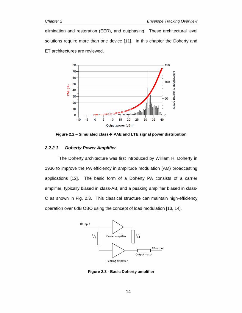
applications [12]. The basic form of a Doherty PA consists of a carrier
amplifier, typically biased in class-AB, and a peaking amplifier biased in class-
C as shown in Fig. 2.3. This classical structure can maintain high-efficiency
operation over 6dB OBO using the concept of load modulation [13, 14].
Figure 2.3 - Basic Doherty amplifier
Chapter 2 Envelope Tracking Overview
15
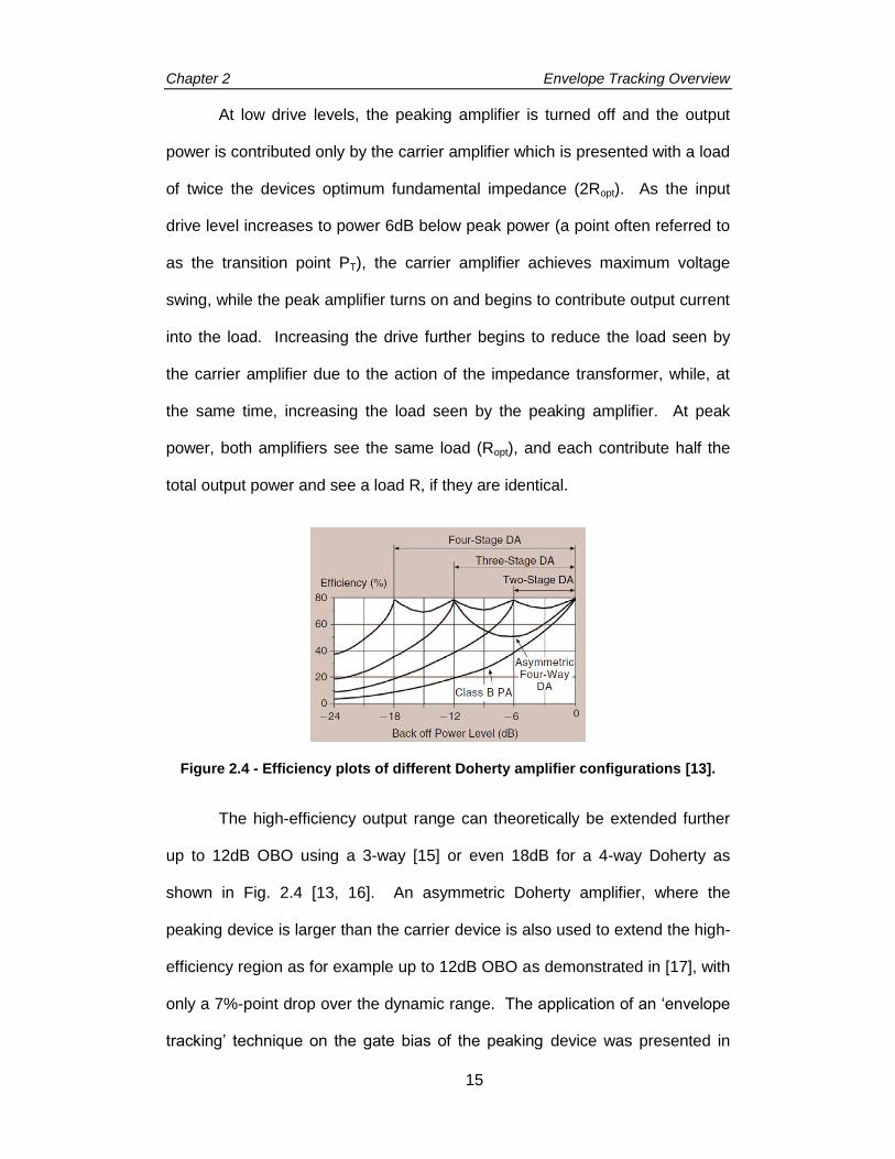
At low drive levels, the peaking amplifier is turned off and the output
power is contributed only by the carrier amplifier which is presented with a load
of twice the devices optimum fundamental impedance (2Ropt). As the input
drive level increases to power 6dB below peak power (a point often referred to
as the transition point PT), the carrier amplifier achieves maximum voltage
swing, while the peak amplifier turns on and begins to contribute output current
into the load. Increasing the drive further begins to reduce the load seen by
the carrier amplifier due to the action of the impedance transformer, while, at
the same time, increasing the load seen by the peaking amplifier. At peak
power, both amplifiers see the same load (Ropt), and each contribute half the
total output power and see a load R, if they are identical.
Figure 2.4 - Efficiency plots of different Doherty amplifier configurations [13].
The high-efficiency output range can theoretically be extended further
up to 12dB OBO using a 3-way [15] or even 18dB for a 4-way Doherty as
shown in Fig. 2.4 [13, 16]. An asymmetric Doherty amplifier, where the
peaking device is larger than the carrier device is also used to extend the high-
efficiency region as for example up to 12dB OBO as demonstrated in [17], with
only a 7%-point drop over the dynamic range. The application of an ‘envelope
tracking’ technique on the gate bias of the peaking device was presented in

Chapter 2 Envelope Tracking Overview
16
[18] to address load modulation issues that are causing the dip in the high-
efficiency region. The work in [19] addresses this dipping phenomenon by
applying ET on the drain bias of the peaking device, and a relatively flat high
efficiency performance was achieved over 18dB of dynamic range in a
simulation environment. However the analysis did not include a fabricated
hardware and the efficiency of the drain supply modulator was not considered.
The main limitation of Doherty PA is the narrow bandwidth introduced
by the use of the quarter wavelength combining transformer. This presents a
challenge in 4G LTE where not only the bandwidth is wider, but with carrier
aggregation, PA’s ideally need to accommodate multiple-bands. Research
focusing on extending the bandwidth of a Doherty PA are ongoing and recent
examples include [20] which is capable of handling a 100MHz instantaneous
bandwidth, and [21] where a 1.5 - 2.14 GHz design was developed
corresponding to a 35% fractional bandwidth.
In [22] a multiband Doherty was designed and fabricated for 1.9, 2.14,
and 2.16GHz obtaining a 60% PAE at 6dB OBO. In a more recent study by
Nghiem et al. a quad-band Doherty PA was developed at 0.96, 1.5, 2.14, and
2.16GHz, although with a relatively lower PAE at 6dB OBO, ranging from 20 to
43% [23]. There are also patented wideband and multiband Doherty PA’s as
shown in [24].
Doherty is currently the architecture of choice for base station power
amplifiers [13], mainly because of its relative simplicity in comparison with
other highly efficient solutions such as ET.
Chapter 2 Envelope Tracking Overview
17
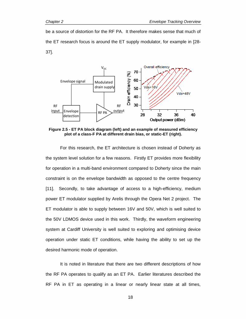
2.2.2.2 Envelope Tracking Power Amplifier
The envelope tracking (ET) architecture is inherently broadband in
comparison with the Doherty, and modulates a device’s DC supply according
to the input envelope magnitude to improve the efficiency during output back-
off. The approach evolved from the envelope elimination and restoration
(EER) amplifier technique by Kahn [25]. In ET, an envelope amplifier is used
to bias the drain of the RF PA based on the input envelope signal as shown in
Fig. 2.4. The envelope information is obtained either through an envelope
detector on the input path or digitally from baseband processing. Its
relationship with the drain bias voltage is defined by an envelope shaping
function to generate the desired ET system-level efficiency shown in Fig. 2.4.
The overall efficiency of an ET PA is calculated as the product of the efficiency
of the RF PA and the envelope amplifier. Therefore to improve the ET PA
efficiency, careful design considerations must be given to both amplifiers.
Currently, the main constraint to implement ET in macro base stations
is the lack of efficient, linear and sufficiently wideband high-power supply
modulators [26]. This limitation is mainly due to the trade-off between the
transistor breakdown voltage and its switching speed, hence ET
implementations tend to be limited to low power applications such as mobile
phones [11]. A simplified version of ET called the average power tracking
(APT) is widely used for mobile phones PA’s where the supply voltage is
changed slowly. However with the advancement of low-power modulators, a
complete ET system is emerging as the future trend, especially with ET’s ability
to work over extended bandwidths and accommodate multi-band operation
[11, 27]. The other issue with the ET supply modulator is that it can potentially
Chapter 2 Envelope Tracking Overview
18
be a source of distortion for the RF PA. It therefore makes sense that much of
the ET research focus is around the ET supply modulator, for example in [28-
37].
Figure 2.5 - ET PA block diagram (left) and an example of measured efficiency plot of a class-F PA at different drain bias, or static-ET (right).
For this research, the ET architecture is chosen instead of Doherty as
the system level solution for a few reasons. Firstly ET provides more flexibility
for operation in a multi-band environment compared to Doherty since the main
constraint is on the envelope bandwidth as opposed to the centre frequency
[11]. Secondly, to take advantage of access to a high-efficiency, medium
power ET modulator supplied by Arelis through the Opera Net 2 project. The
ET modulator is able to supply between 16V and 50V, which is well suited to
the 50V LDMOS device used in this work. Thirdly, the waveform engineering
system at Cardiff University is well suited to exploring and optimising device
operation under static ET conditions, while having the ability to set up the
desired harmonic mode of operation.
It is noted in literature that there are two different descriptions of how
the RF PA operates to qualify as an ET PA. Earlier literatures described the
RF PA in ET as operating in a linear or nearly linear state at all times,
Chapter 2 Envelope Tracking Overview
19
differentiating it from polar amplifiers [5, 38-41]. In such linear operation, the
modulated drain supply has minimal impact on the output envelope shape. In
later literatures, the terms envelope tracking amplifier and polar amplifier are
used interchangeably where the nonlinear operation of the RF PA is utilised by
operating it in compression at all time for efficiency enhancement, as described
in [26, 42-46].
For this research, the class-AB PA that is typically used in ET
architectures is replaced with a class-F PA to boost the maximum available
efficiency. In order to generate the necessary harmonic current components,
class-F mode requires that the device operates in a specific degree of
compression at all bias setting within the ET range. Therefore the term ‘ET’
used in this research includes the compressed condition in which the device
operates in a nonlinear state.
2.3 Research Areas in Envelope Tracking Power
Amplifiers
2.3.1 Modulated Drain Supply Generation
As this is the current limitation that is holding back ET from wide
deployments in macro base stations, much of the research in ET has focused
and continues to focus on the modulated bias signal path rather than on the
optimisation of the RF PA within the ET architecture [47]. The DC modulation
path consists of 2 main components - envelope generation and the supply
modulator itself. This DC modulation topic alone is a large research area as
seen in [34, 35, 48-50] and is not within the scope of this work. However, it is
worth highlighting 2 recent developments in this area which are relevant to this
PhD work.

Chapter 2 Envelope Tracking Overview
20
The first of these is [36] where a new technique was developed for the
modulated drain supply utilising a sinking current. Using this method on a
class-AB PA at 889MHz, a 60% drain efficiency was achieved for a 6.5dB
PAPR 10MHz LTE signal at 40.2dBm output power. The results obtained here
are under similar conditions used for this PhD work, namely the frequency,
output power, and the signal PAPR. Furthermore, one of the objectives of this
PhD work is to compare the performance of the traditional class-AB
implementation in ET with class-F, as described in Chapters 3 and 4.
Therefore the work in [36] provides a good baseline, even though it uses a
GaN device instead of LDMOS.
The second relevant piece of work in this modulator topic is the work
presented by Yusoff in [51, 52] where a simple and low-cost technique to
generate the modulated drain supply called auxiliary envelope tracking (AET)
was presented. In this technique the DC and AC components of the
modulated drain supply are generated separately and a broadband RF
transformer is used to combine them and dynamically bias the device. The
magnitude and phase of the envelope amplifier output which amplifies the AC
path can be varied to reduce IM3 distortion products. The limitation in this
technique, as published, is the limited flexibility in controlling the envelope
shaping function and the limited dynamic range of the detector diode. One of
the objectives of this PhD work is to use ET as a linearising method using the
envelope shaping function which would address the limitations described
above, and shall be discussed in Chapters 4 and 5.
Chapter 2 Envelope Tracking Overview
21
2.3.2 Use of High-Efficiency Modes in Envelope Tracking PA
The RF PA in an ET system typically operates in class-AB mode due to
its linearity advantage [28]. However other high-efficiency modes of operation
have been used in an ET architecture that are discussed in literature. In [53] a
class-F-1 mode is used on a GaN HEMT device optimised for an ET
architecture achieving more than 70% efficiency over a bandwidth of 920-
960MHz. However the measured efficiency was of the RF PA alone without
the drain modulator, obtained from CW measurements at individual drain bias
points.
Alavi et al. used a class-B and class-J* “hybrid” in an ET setting in [44],
utilising the drain-to-source capacitance (CDS) variation with drain voltage to
tune the fundamental and 2nd harmonic impedances between the 2 PA modes.
A static ET experiment where CW measurements were made at individual
drain bias points using load-pull on a 2W LDMOS device at 2.14GHz achieved
an average PAE of 64% at 7.8dB output back-off. However once again this is
only the efficiency of the RF PA alone under CW excitation. The actual ET
dynamic bias effect was not observed and the efficiency of the drain supply
modulator was not included.
The class-J mode PA was also used by Kimball et al. in an ET system
in [45], this time in combination with a class-E type of operation using a GaN
HFET for a W-CDMA base station. Using a signal with 7.67dB PAPR, the
average combined efficiency for both the RF PA and the drain modulator was
50.7% at 37.2W average output power. This is another good baseline
reference for comparison with this PhD work.
Chapter 2 Envelope Tracking Overview
22
In [46] Kim et al. presented the use of a class-F-1 mode, fully integrated
with an ET modulator for a 3G LTE base station design using a 60W peak
power GaN device, achieving 44% drain efficiency at 3.54GHz. However, it is
observed that the class-F-1 GaN RF PA efficiency before ET was already below
60%. This PhD work aims to use the waveform engineering system [54] to
systematically optimise the RF PA design for ET applications to achieve a
higher baseline efficiency as demonstrated in [55] for a class-F-1, and this is
described in Chapter 4.
In [56] a class-F-1 PA in ET was developed using GaN MMIC at 10GHz.
With the RF PA optimised for efficiency at average power and trading-off the
efficiency at peak power, the average efficiency achieved with an ET
modulator was 54.4% for a 6.6dB PAPR LTE signal. The RF PA optimisation
was done through fundamental load-pull while the harmonic terminations were
determined from simulations.
2.3.3 Use of LDMOS in ET
In high-power ET applications outlined in the previous section, GaN
devices are typically used in preference to LDMOS. The large output
capacitance (CDS) and on-resistance (RON) associated with LDMOS causes
reduced efficiency in comparison to GaN. However, the low cost of LDMOS
makes it an attractive solution for <3GHz applications and as of 2014 it
accounted for 95% of the base station market [26]. Previous ET PA
realisations that utilised LDMOS devices as the RF PA obtained lower
efficiency numbers compared to their GaN counterpart. For example in [29]
the achieved average PAE was 40% for a 7.6dB-PAPR 3.84MHz-bandwidth
W-CDMA signal at 27W output power. However, this was obtained with a
Chapter 2 Envelope Tracking Overview
23
64%-efficient RF PA that was optimised at peak power. The use of a highly-
efficient PA mode with harmonic termination optimised at average power could
have increased this efficiency further.
In [57] a static ET evaluation from CW measurements was performed
on a 10W LDMOS device, this time with 2nd harmonic tuning for efficiency
optimisation of a class-AB operation at 2.14GHz. The drain efficiency obtained
from this technique was 50% for approximately 5dB of input power back-off.
However, this number is for the RF PA alone and a full ET system test was not
performed.
2.3.4 PA Linearisation using Baseband Injection for ET Applications
The linearity aspect of a PA in some applications takes precedence
over efficiency, such as those used for base stations due to stringent
regulations in spectral interference [5]. Almost all of the ET PAs described
above rely heavily on digital pre-distortion (DPD) to achieve the necessary
linearity. It should be remembered however that DPD should be considered as
‘the last resort’ in linearising a PA [58] and designing PAs with maximum ‘raw’
linearity while still remaining highly efficient remains the ultimate objective.
The linearity performance of a transistor device technology, such as
LDMOS, is heavily affected by the impedance presented at baseband
frequencies [59]. The usual solution to this is careful design of bias networks
that present very low, ideally short-circuit impedances to baseband
components. It has been shown however in [60] that it is possible to improve
the linearity of a transistor by injecting a baseband signal into the output of the
device operating in a compressed state. The injected baseband signal will

Chapter 2 Envelope Tracking Overview
24
produce mixing products and depending on the magnitude and phase of the
baseband signal, the mixing products have the potential to cancel out odd-
order intermodulation products of the PA. It makes sense therefore to explore
the idea of achieving such linearity improvement and efficiency enhancement
simultaneously through the application of specific ET signals.
The use of waveform engineering in investigating AM-AM linearisation
methods for PAs was first shown in [61] using an active IF load-pull system
where the linearising baseband signal was presented in the form of a negative
impedance that lies outside the Smith chart. This impedance, when presented
to a drain of a 10W GaN device, was able to suppress the 3rd and 5th order
intermodulation products under modulated excitations [62]. Further work in
[63] developed a systematic formulation of the even-order baseband
coefficients to suppress the intermodulation products of a class-AB mode PA
operating in compression, which was shown to be independent of envelope
complexity [64], envelope bandwidth [65], and FET device technology [66].
The engineered injected baseband signal linearises the device
transconductance, which is derived from the relationship between the output
drain current versus the input voltage [67].
In terms of implementation, the previous work of baseband injection in
[61-66] used arbitrary waveform generators (AWG) to independently generate
the baseband signal and combine it with the DC bias through a diplexer at the
drain for PA linearisation. This is possible as long as the input envelope signal
shape is repetitive, known and well-defined, as would be the case for example
if the RF input excitation is constructed using discrete tones. However when
complex, continuous modulation schemes such as LTE and W-CDMA signals

Chapter 2 Envelope Tracking Overview
25
are used, while the linearising baseband transfer function and formulated
coefficients still hold, the time-domain baseband signal itself cannot be easily
generated independently with an AWG and be made coherent with the random
input envelope, but rather it must be sampled off the input. In an ET system,
that linearising baseband transfer function takes the form of an envelope
shaping function of the drain supply modulator.
While the intended purpose of the aforementioned research work was
ET implementation, the effect of the baseband injection on efficiency was not
previously investigated due to the unavailability of an ET modulator.
Therefore, this PhD work aims to ‘close the loop’ of that study by investigating
the possibility of using ET as a baseband injection signal simultaneously for PA
linearisation and analyse its trade-off with efficiency.
2.4 State-of-the-Art Envelope Tracking Power Amplifiers
Recent works in this field have produced further improved efficiency
numbers or higher frequency of operation. In [68] a GaN device operating in
class-AB was used in ET at 780MHz by Yan et al. The measured drain
efficiencies were 69% and 60% for a 6.6dB-PAPR 5MHz-bandwidth 29W-
power WCDMA and a 7.5dB-PAPR 10MHz-bandwidth 23W-power LTE signal,
respectively.
A GaN HEMT operating in class-E is used in [69] in an ET system at
2.6GHz. With the RF PA having a drain efficiency of 74% and the ET
modulator at 92% efficiency, the overall ET efficiency was 60% when a 6.5dB
PAPR 10MHz LTE signal was applied producing a 40W average output power.

Chapter 2 Envelope Tracking Overview
26
In [70] an ET PA utilising a GaN device operating in inverse class-F at
880MHz was able to produce a PAE of 53% at 7.4W output power for a 6.6dB
PAPR 20MHz LTE signal.
A higher bandwidth was achieved in [71] where an X-band GaN MMIC
PA was used in ET for a 60MHz LTE signal with 6.6dB PAPR. With the RF PA
operating in class-E at 9.23GHz, the overall PAE achieved was 35% at 1.1W
average output power.
These state-of-the-art ET PA’s shall be used as a benchmark for the ET
PA developed in this PhD work.
2.5 Conclusions & New Research Opportunities
Envelope tracking is a well-covered topic in research with the
introduction of 4G LTE and heterogeneous networks. Wideband and
multiband operations present a challenge for the current practice in base
stations where the current standard Doherty amplifiers are widely used.
Although the research in ET is well-covered, there are still opportunities for
new research areas within the ET field, and for this PhD work to address some
gaps in the literature.
The first research opportunity is the use of a high-voltage LDMOS
device technology in ET. Most ET implementations use GaN devices, except
for a small few, and the ones that used LDMOS did not achieve high efficiency
numbers with conventional class-AB mode.
The second opportunity is the use of class-F mode in ET. As described
in Section 2.3.2, ET typically uses class-AB PA’s and most of the work

Chapter 2 Envelope Tracking Overview
27
involving high-efficiency modes in ET used class-F-1 mode. The only work that
the author is aware of using class-F in ET at the time of writing is [72] where a
continuous-mode class-F approach is proposed. However, that work only
presented simulation results and no actual measurements were performed.
Thirdly, there is an opportunity to fully research the use of continuous
mode PA’s in ET as this has not been analysed in detail and tested with a
hardware before. This is a new topic and presents an attractive solution for
wideband ET implementation, if successful. It is also interesting to understand
how such structures would respond to baseband linearisation, within an ET
environment.
The fourth opportunity is to use waveform engineering to optimise the
RF PA in an ET system. This approach has been successfully used in high-
efficiency and high-bandwidth PA design as well as device characterisation
and modelling previously, but has not been used in designing an RF PA for ET
applications.
2.6 References
[1] R. Caverly, F. Raab, and J. Staudinger, "High-Efficiency Power Amplifiers," Microwave Magazine, IEEE, vol. 13, pp. S22-S32, 2012.
[2] L. M. Correia, D. Zeller, O. Blume, D. Ferling, Y. Jading, G. I, et al., "Challenges and enabling technologies for energy aware mobile radio networks," IEEE Communications Magazine, vol. 48, pp. 66-72, 2010.
[3] G. Koutitas and P. Demestichas, "A Review of Energy Efficiency in Telecommunication Networks," Telfor Journal, vol. 2, 2010.
[4] M. Eron, B. Kim, F. Raab, R. Caverly, and J. Staudinger, "The Head of the Class," Microwave Magazine, IEEE, vol. 12, pp. S16-S33, 2011.
[5] S. C. Cripps, RF Power Amplifiers for Wireless Communications: Artech House, 2006.
Chapter 2 Envelope Tracking Overview
28
[6] N. O. Sokal, "RF power amplifiers-classes A through S," in Electro/95 International. Professional Program Proceedings., 1995, pp. 335-400.
[7] A. Sheikh, C. Roff, J. Benedikt, P. J. Tasker, B. Noori, J. Wood, et al., "Peak Class F and Inverse Class F Drain Efficiencies Using Si LDMOS in a Limited Bandwidth Design," IEEE Microwave and Wireless Components Letters, vol. 19, pp. 473-475, 2009.
[8] V. Carrubba, A. L. Clarke, M. Akmal, J. Lees, J. Benedikt, P. J. Tasker, et al., "The Continuous Class-F Mode Power Amplifier," in Microwave Conference (EuMC), 2010 European, 2010, pp. 1674-1677.
[9] V. Carrubba, J. Lees, J. Benedikt, P. J. Tasker, and S. C. Cripps, "A novel highly efficient broadband continuous class-F RFPA delivering 74% average efficiency for an octave bandwidth," in Microwave Symposium Digest (MTT), 2011 IEEE MTT-S International, 2011, pp. 1-4.
[10] F. H. Raab, "Maximum efficiency and output of class-F power amplifiers," IEEE Transactions on Microwave Theory and Techniques, vol. 49, pp. 1162-1166, 2001.
[11] P. Asbeck and Z. Popovic, "ET Comes of Age: Envelope Tracking for Higher-Efficiency Power Amplifiers," Microwave Magazine, IEEE, vol. 17, pp. 16-25, 2016.
[12] W. H. Doherty, "A New High Efficiency Power Amplifier for Modulated Waves," Proceedings of the Institute of Radio Engineers, vol. 24, pp. 1163-1182, 1936.
[13] R. Pengelly, C. Fager, and M. Ozen, "Doherty's Legacy: A History of the Doherty Power Amplifier from 1936 to the Present Day," IEEE Microwave Magazine, vol. 17, pp. 41-58, 2016.
[14] B. Kim, K. Ildu, and M. Junghwan, "Advanced Doherty Architecture," Microwave Magazine, IEEE, vol. 11, pp. 72-86, 2010.
[15] F. H. Raab, "Efficiency of Doherty RF Power-Amplifier Systems," IEEE Transactions on Broadcasting, vol. BC-33, pp. 77-83, 1987.
[16] K. J. Cho, W. J. Kim, J. Y. Kim, J. H. Kim, and S. P. Stapleton, "N-Way Distributed Doherty Amplifier with an Extended Efficiency Range," in 2007 IEEE/MTT-S International Microwave Symposium, 2007, pp. 1581-1584.
[17] M. Iwamoto, A. Williams, C. Pin-Fan, A. G. Metzger, L. E. Larson, and P. M. Asbeck, "An extended Doherty amplifier with high efficiency over a wide power range," IEEE Transactions on Microwave Theory and Techniques, vol. 49, pp. 2472-2479, 2001.
Chapter 2 Envelope Tracking Overview
29
[18] K. Ildu and B. Kim, "A 2.655 GHz 3-stage Doherty power amplifier using envelope tracking technique," in Microwave Symposium Digest (MTT), 2010 IEEE MTT-S International, 2010, pp. 1496-1499.
[19] M. Thian, P. Gardner, M. Thian, and P. Gardner, "Envelope-tracking-based Doherty power amplifier," International Journal of Electronics, vol. 97, pp. 525-530, 5 2010.
[20] C. Ma, W. Pan, S. Shao, C. Qing, and Y. Tang, "A Wideband Doherty Power Amplifier With 100 MHz Instantaneous Bandwidth for LTE-Advanced Applications," IEEE Microwave and Wireless Components Letters, vol. 23, pp. 614-616, 2013.
[21] K. Bathich, A. Z. Markos, and G. Boeck, "A wideband GaN Doherty amplifier with 35 % fractional bandwidth," in Microwave Conference (EuMC), 2010 European, 2010, pp. 1006-1009.
[22] A. M. M. Mohamed, S. Boumaiza, and R. R. Mansour, "Reconfigurable Doherty Power Amplifier for Multifrequency Wireless Radio Systems," IEEE Transactions on Microwave Theory and Techniques, vol. 61, pp. 1588-1598, 2013.
[23] X. A. Nghiem, J. Guan, T. Hone, and R. Negra, "Design of Concurrent Multiband Doherty Power Amplifiers for Wireless Applications," IEEE Transactions on Microwave Theory and Techniques, vol. 61, pp. 4559-4568, 2013.
[24] A. Grebennikov and S. Bulja, "High-Efficiency Doherty Power Amplifiers: Historical Aspect and Modern Trends," Proceedings of the IEEE, vol. 100, pp. 3190-3219, 2012.
[25] L. R. Kahn, "Single-Sideband Transmission by Envelope Elimination and Restoration," Proceedings of the IRE, vol. 40, pp. 803-806, 1952.
[26] Z. Wang, Envelope Tracking Power Amplifiers for Wireless Communications: Artech House, 2014.
[27] B. Kim, "Advanced linear PA architectures for handset applications," in Wireless Symposium (IWS), 2013 IEEE International, 2013, pp. 1-1.
[28] K. Bumman, M. Junghwan, and K. Ildu, "Efficiently Amplified," Microwave Magazine, IEEE, vol. 11, pp. 87-100, 2010.
[29] P. Draxler, S. Lanfranco, D. Kimball, C. Hsia, J. Jeong, J. van de Sluis, et al., "High Efficiency Envelope Tracking LDMOS Power Amplifier for W-CDMA," in Microwave Symposium Digest, 2006. IEEE MTT-S International, 2006, pp. 1534-1537.
[30] J. Jeong, D. F. Kimball, M. Kwak, P. Draxler, C. Hsia, C. Steinbeiser, et al., "High-Efficiency WCDMA Envelope Tracking Base-Station Amplifier
Chapter 2 Envelope Tracking Overview
30
Implemented with GaAs HVHBTs," IEEE Journal of Solid-State Circuits, vol. 44, pp. 2629-2639, 2009.
[31] I. Kim, J. Kim, J. Moon, and B. Kim, "Optimized Envelope Shaping for Hybrid EER Transmitter of Mobile WiMAX - Optimized ET Operation," IEEE Microwave and Wireless Components Letters, vol. 19, pp. 335-337, 2009.
[32] D. Kimball, P. Draxler, J. Jeong, C. Hsia, S. Lanfranco, W. Nagy, et al., "50% PAE WCDMA basestation amplifier implemented with GaN HFETs," in IEEE Compound Semiconductor Integrated Circuit Symposium, 2005. CSIC '05., 2005, p. 4 pp.
[33] D. Kimball, J. J. Yan, P. Theilmanrr, M. Hassan, P. Asbeck, and L. Larson, "Efficient and wideband envelope amplifiers for envelope tracking and polar transmitters," in Power Amplifiers for Wireless and Radio Applications (PAWR), 2013 IEEE Topical Conference on, 2013, pp. 13-15.
[34] V. Yousefzadeh, E. Alarcon, and D. Maksimovic, "Three-level buck converter for envelope tracking applications," IEEE Transactions on Power Electronics, vol. 21, pp. 549-552, 2006.
[35] M. Vasic, P. Cheng, O. Garcia, J. A. Oliver, P. Alou, J. A. Cobos, et al., "The Design of a Multilevel Envelope Tracking Amplifier Based on a Multiphase Buck Converter," IEEE Transactions on Power Electronics, vol. 31, pp. 4611-4627, 2016.
[36] J. Kim, J. Moon, J. Son, S. Jee, J. Lee, J. Cha, et al., "Highly efficient envelope tracking transmitter by utilizing sinking current," in Microwave Conference (EuMC), 2011 41st European, 2011, pp. 1197-1200.
[37] W. Zhancang, "Demystifying Envelope Tracking: Use for High-Efficiency Power Amplifiers for 4G and Beyond," Microwave Magazine, IEEE, vol. 16, pp. 106-129, 2015.
[38] C. Buoli, A. Abbiati, and D. Riccardi, "Microwave power amplifier with "envelope controlled" drain power supply," in Microwave Conference, 1995. 25th European, 1995, pp. 31-35.
[39] G. Hanington, C. Pin-Fan, P. M. Asbeck, and L. E. Larson, "High-efficiency power amplifier using dynamic power-supply voltage for CDMA applications," IEEE Transactions on Microwave Theory and Techniques, vol. 47, pp. 1471-1476, 1999.
[40] E. McCune, "Envelope Tracking or Polar - Which Is It? [Microwave Bytes]," IEEE Microwave Magazine, vol. 13, pp. 34-56, 2012.
[41] E. McCune, Dynamic Power Supply Transmitters: Cambridge University Press, 2015.
Chapter 2 Envelope Tracking Overview
31
[42] G. F. Collins, J. Wood, and B. Woods, "Challenges of power amplifier design for envelope tracking applications," in Power Amplifiers for Wireless and Radio Applications (PAWR), 2015 IEEE Topical Conference on, 2015, pp. 1-3.
[43] K. Bumman, K. Jungjoon, K. Dongsu, S. Junghwan, C. Yunsung, K. Jooseung, et al., "Push the Envelope: Design Concepts for Envelope-Tracking Power Amplifiers," Microwave Magazine, IEEE, vol. 14, pp. 68-81, 2013.
[44] M. S. Alavi, F. van Rijs, M. Marchetti, M. Squillante, T. Zhang, S. J. Theeuwen, et al., "Efficient LDMOS device operation for envelope tracking amplifiers through second harmonic manipulation," in Microwave Symposium Digest (MTT), 2011 IEEE MTT-S International, 2011, pp. 1-1.
[45] D. F. Kimball, J. Jeong, H. Chin, P. Draxler, S. Lanfranco, W. Nagy, et al., "High-Efficiency Envelope-Tracking W-CDMA Base-Station Amplifier Using GaN HFETs," Microwave Theory and Techniques, IEEE Transactions on, vol. 54, pp. 3848-3856, 2006.
[46] J. H. Kim, G. D. Jo, J. H. Oh, Y. H. Kim, K. C. Lee, J. H. Jung, et al., "High-Efficiency Envelope-Tracking Transmitter With Optimized Class-F-1 Amplifier and 2-bit Envelope Amplifier for 3G LTE Base Station," IEEE Transactions on Microwave Theory and Techniques, vol. 59, pp. 1610-1621, 2011.
[47] G. F. Collins, J. Fisher, F. Radulescu, J. Barner, S. Sheppard, R. Worley, et al., "Power Amplifier Design Optimized for Envelope Tracking," in Compound Semiconductor Integrated Circuit Symposium (CSICs), 2014 IEEE, 2014, pp. 1-4.
[48] Q. Jin, X. Ruan, X. Ren, Y. Wang, Y. Leng, and C. Tse, "Series-Parallel Form Switch-Linear Hybrid Envelope-Tracking Power Supply to Achieve High Efficiency," IEEE Transactions on Industrial Electronics, vol. PP, pp. 1-1, 2016.
[49] V. I. Kumar and S. Kapat, "Mixed-signal hysteretic internal model control of buck converters for ultra-fast envelope tracking," in 2016 IEEE Applied Power Electronics Conference and Exposition (APEC), 2016, pp. 3224-3230.
[50] J. S. Paek, Y. S. Youn, J. H. Choi, D. S. Kim, J. H. Jung, Y. H. Choo, et al., "An RF-PA supply modulator achieving 83% efficiency and -136dBm/Hz noise for LTE-40MHz and GSM 35dBm applications," in 2016 IEEE International Solid-State Circuits Conference (ISSCC), 2016, pp. 354-355.
[51] Z. Yusoff, J. Lees, J. Benedikt, P. J. Tasker, and S. C. Cripps, "Linearity improvement in RF power amplifier system using integrated

Chapter 2 Envelope Tracking Overview
32
Auxiliary Envelope Tracking system," in Microwave Symposium Digest (MTT), 2011 IEEE MTT-S International, 2011, pp. 1-4.
[52] Z. Yusoff, J. Lees, M. A. Chaudhary, V. Carrubba, C. Heungjae, P. Tasker, et al., "Simple and low-cost tracking generator design in envelope tracking radio frequency power amplifier system for WCDMA applications," Microwaves, Antennas & Propagation, IET, vol. 7, pp. 802-808, 2013.
[53] W. Zhancang, "A class-F-1 GaN HEMT power amplifier optimized for envelope tracking with gain-efficiency trajectory analysis and comparison," in Microwaves, Communications, Antennas and Electronics Systems (COMCAS), 2013 IEEE International Conference on, 2013, pp. 1-4.
[54] P. J. Tasker, "Practical waveform engineering," Microwave Magazine, IEEE, vol. 10, pp. 65-76, 2009.
[55] P. Wright, A. Sheikh, C. Roff, P. J. Tasker, and J. Benedikt, "Highly efficient operation modes in GaN power transistors delivering upwards of 81% efficiency and 12W output power," in Microwave Symposium Digest, 2008 IEEE MTT-S International, 2008, pp. 1147-1150.
[56] G. Collins, J. Fisher, F. Radulescu, J. Barner, S. Sheppard, R. Worley, et al., "C-band and X-band class F, F-1 GaN MMIC PA design for envelope tracking systems," in Microwave Conference (EuMC), 2015 European, 2015, pp. 1172-1175.
[57] E. Cipriani, P. Colantonio, F. Giannini, R. Giofre, and L. Piazzon, "Envelope Tracking Technique Applied on a 10W 2(nd) Harmonic Tuned Power Amplifier at 2.14 GHz," 2009 European Microwave Conference, Vols 1-3, pp. 1429-1432, 2009.
[58] R. S. Pengelly, W. Pribble, and T. Smith, "Inverse Class-F Design Using Dynamic Loadline GaN HEMT Models to Help Designers Optimize PA Efficiency [Application Notes]," Microwave Magazine, IEEE, vol. 15, pp. 134-147, 2014.
[59] J. Brinkhoff and A. E. Parker, "Effect of baseband impedance on FET intermodulation," Microwave Theory and Techniques, IEEE Transactions on, vol. 51, pp. 1045-1051, 2003.
[60] J. Brinkhoff, A. E. Parker, and M. Leung, "Baseband impedance and linearization of FET circuits," Microwave Theory and Techniques, IEEE Transactions on, vol. 51, pp. 2523-2530, 2003.
[61] J. Lees, M. Akmal, S. Bensmida, S. Woodington, S. Cripps, J. Benedikt, et al., "Waveform engineering applied to linear-efficient PA design," in Wireless and Microwave Technology Conference (WAMICON), 2010 IEEE 11th Annual, 2010, pp. 1-5.
Chapter 2 Envelope Tracking Overview
33
[62] M. Akmal, V. Carrubba, J. Lees, S. Bensmida, J. Benedikt, K. Morris, et al., "Linearity enhancement of GaN HEMTs under complex modulated excitation by optimizing the baseband impedance environment," in Microwave Symposium Digest (MTT), 2011 IEEE MTT-S International, 2011, pp. 1-4.
[63] F. L. Ogboi, P. J. Tasker, M. Akmal, J. Lees, J. Benedikt, S. Bensmida, et al., "A LSNA configured to perform baseband engineering for device linearity investigations under modulated excitations," in Microwave Conference (EuMC), 2013 European, 2013, pp. 684-687.
[64] F. L. Ogboi, P. J. Tasker, M. Akmal, J. Lees, J. Benedikt, S. Bensmida, et al., "Investigation of Various Envelope Complexity Linearity under Modulated Stimulus Using a New Envelope Formulation Approach," in Compound Semiconductor Integrated Circuit Symposium (CSICs), 2014 IEEE, 2014, pp. 1-4.
[65] F. L. Ogboi, P. J. Tasker, M. Akmal, J. Lees, J. Benedikt, S. Bensmida, et al., "High bandwidth investigations of a baseband linearization approach formulated in the envelope domain under modulated stimulus," in Microwave Conference (EuMC), 2014 44th European, 2014, pp. 1305-1308.
[66] F. L. Ogboi, P. Tasker, Z. Mohkti, J. Lees, J. Benedikt, S. Bensmida, et al., "Sensitivity of AM/AM linearizer to AM/PM distortion in devices," in Microwave Measurement Conference (ARFTG), 2014 83rd ARFTG, 2014, pp. 1-4.
[67] F. Chun-Wah and K. K. M. Cheng, "Theoretical and experimental study of amplifier linearization based on harmonic and baseband signal injection technique," Microwave Theory and Techniques, IEEE Transactions on, vol. 50, pp. 1801-1806, 2002.
[68] J. J. Yan, P. Theilmann, and D. F. Kimball, "A High Efficiency 780 MHz GaN Envelope Tracking Power Amplifier," in 2012 IEEE Compound Semiconductor Integrated Circuit Symposium (CSICS), 2012, pp. 1-4.
[69] H. Tango, T. Hashinaga, K. Totani, H. Kuriyama, Y. Hamada, and T. Asaina, "A 60% efficient envelope tracking PA for 40W, 2.6GHz LTE base station with in/output harmonic tuning," in Microwave Symposium Digest (IMS), 2013 IEEE MTT-S International, 2013, pp. 1-4.
[70] Y. Liu, C. S. Yoo, J. Fairbanks, J. Yan, D. Kimball, and P. Asbeck, "A 53% PAE envelope tracking GaN power amplifier for 20MHz bandwidth LTE signals at 880MHz," in 2016 IEEE Topical Conference on Power Amplifiers for Wireless and Radio Applications (PAWR), 2016, pp. 30-32.
[71] P. T. Theilmann, J. J. Yan, C. Vu, J. S. Moon, H. P. Moyer, and D. F. Kimball, "A 60MHz Bandwidth High Efficiency X-Band Envelope

Chapter 2 Envelope Tracking Overview
34
Tracking Power Amplifier," in 2013 IEEE Compound Semiconductor Integrated Circuit Symposium (CSICS), 2013, pp. 1-4.
[72] B. Merrick and T. J. Brazil, "Analysis of the integration of envelope tracking with Continuous Class F amplifiers," in Integrated Nonlinear Microwave and Millimetre-Wave Circuits (INMMIC), 2012 Workshop on, 2012, pp. 1-3.
Chapter 3 Class-F PA Behaviour in a Variable Drain Setting
35
Chapter 3 Class-F Power Amplifier Behaviour in a Variable Drain Bias Setting
3.1 Introduction
In the previous chapter, the efficiency aspect of a power amplifier (PA)
is discussed in two types of implementation, firstly improving the efficiency at
peak power using high efficiency modes and secondly improving efficiency
during output back-off (OBO) through the use of high-efficiency architectures.
This research work focuses on integrating a high efficiency mode, namely
class-F into a high-efficiency architecture, namely envelope tracking (ET).
Such integration starts with analysing the behaviour of a class-F mode PA in a
variable drain bias setting, which is the focus of this chapter.
The first objective of this chapter is to analyse the requirements for
maintaining a class-F PA mode in a variable drain setting which represents an
envelope tracking environment, and to understand the impact of the variation
in device output capacitance (CDS) with drain supply on efficiency when the
class-F amplifier impedance environment is optimised at a single drain bias
(VDS) setting.
The second objective is to analyse the linearity performance of different
PA modes in an ET environment, and the possible trade-offs with efficiency

Chapter 3 Class-F PA Behaviour in a Variable Drain Setting
36
through the use of different envelope shaping functions. The experimental
investigation of these effects on class-AB and class-F PA modes is performed
using a 10W LDMOS device. The use of waveform engineering to formulate a
shaping function to linearise the ET PA is then compared to previous work of
using baseband injection as a PA linearising method [1].
This chapter begins by describing the measurement system and device
under test used in this work. This is followed by the investigation of class-F
behaviour in ET, with simulation and experimental results. The subsequent
experiment then looks at what is achievable and the trade-offs possible when
using different shaping functions, followed by a discussion on the comparison
with baseband injection work. A comparison with class-AB mode of operation
is shown in each experiment, as it is the current PA mode usually used in ET
PAs [2].
3.2 Measurement System and Device under Test
3.2.1 Waveform Engineering Measurement System
The waveform engineering approach [3] which was developed at
Cardiff University uses an active load-pull system to construct the desired
current and voltage waveforms at the transistor’s intrinsic current generator
plane. This is achieved by synthesizing the required fundamental and
harmonic load impedances at any bias point, hence setting up any PA mode of
operation. This can be thought of as emulating a harmonic balance simulation
through actual measurement [4].
The active load-pull measurement system is described in detail in
Appendix A. It is based around an Agilent N5242A PNA-X Nonlinear Vector

Chapter 3 Class-F PA Behaviour in a Variable Drain Setting
37
Network Analyser (NVNA) as a receiver. The load-pull system is run using the
Mesuro software environment which enables 3-harmonic load search, multi-
parameter sweeps, and 3 layers of de-embedding. No input matching was
applied on the device input side in this research work, instead the input drive
level was increased accordingly to overcome the mismatch losses to arrive at
the desired delivered input power level. The fundamental frequency for this
work was set at 900MHz.
Figure 3.1 - Active load-pull system and the device under test
3.2.2 Device under Test and De-embedding
The transistor device used in this work was a packaged 10W high
voltage LDMOS (HVLDMOS) from Freescale (now NXP) with a gate width of
5.2 mm. As it was a test device made for this research work, it only had a
single bond wire each at the gate and the drain. The knee voltage was
approximately 10V while its maximum operating drain voltage of 50V provided
higher output impedance compared to a 30V device of the same power
capacity. To avoid the knee and breakdown regions, the ET drain bias range
was defined to be from 16V to 48V in 4V steps. Hence there were 9 static ET

Chapter 3 Class-F PA Behaviour in a Variable Drain Setting
38
bias points where the measurements were performed, namely: 16V, 20V, 24V,
28V, 32V, 36V, 40, 44V, and 48V.
The device model used in Keysight ADS simulation software was
provided by Freescale. The device static CDS values for different drain
voltages was also provided, which therefore enabled a static de-embedding
process from the device package to the device current generator plane for a
particular bias. The model was found to correlate well with the actual device
and this verification process is described in more detail in Appendix A.
For load-pull measurements that involved drain bias variation, a two-
layer de-embedding approach was used to obtain the waveform information at
the device current generator plane. The first layer was a fixed de-embedding
that includes the test fixture and the device package. The second layer was a
bias-dependent de-embedding to cater for the changing CDS value with the
applied drain bias. For this work the feedback capacitance between the gate
and the drain (CGD) was not considered as the value was too small and can be
neglected.
3.3 Maintaining Class-F in a Variable Drain Setting
This section investigates the requirement in maintaining a class-F PA in
a variable drain setting and the efficiency degradation when it is optimised at
one bias point due to the device output capacitance (CDS).
3.3.1 Methodology
For this analysis, three scenarios were investigated in order to
understand the impact of CDS on drain efficiency in an ET setting. Firstly, when
the class-F fundamental impedance environment was optimised at each drain
Chapter 3 Class-F PA Behaviour in a Variable Drain Setting
39
voltage throughout the ET range (best case scenario); secondly, when the
class-F mode was optimised at the maximum drain voltage of 48V; and thirdly,
when the class-F mode was optimised at a static value of VDS=28V, which
represents an average voltage value during output back-off condition where
the class-F PA would spend most of its time, as demonstrated in [5] for an LTE
signal. A similar approach was used in [6], but with a class-B/J mode and only
addressed the first two scenarios, namely optimised at each drain voltage and
at maximum drain voltage.
To optimise a class-F impedance at any drain bias point, a load-pull
search was performed to find the optimum load for efficiency at 1dB
compression level. The constant compression level was chosen in this
experiment as it provided a standardised search criterion and was close to the
maximum efficiency point. Using the appropriate CDS de-embedding (an
example is described in Appendix A), the load-pull system was then used to
engineer the class-F voltage and current waveforms at the device current
generator plane. The desired class-F waveforms were established for each
optimisation step – thus it can be said that the class-F operational condition
established through waveform engineering and dynamic load-line manipulation
relative to the I-V space, provided a very robust way of normalizing the
measurement, and demonstrating that class-F operation was being maintained
at different bias levels.
Finally, the experiment was repeated on a class-AB mode using the
same method and scenarios. For this mode the gate was biased such that the
quiescent point was at approximately 3% of the device’s maximum current to
retain a high efficiency number. The 2nd harmonic output current was shorted
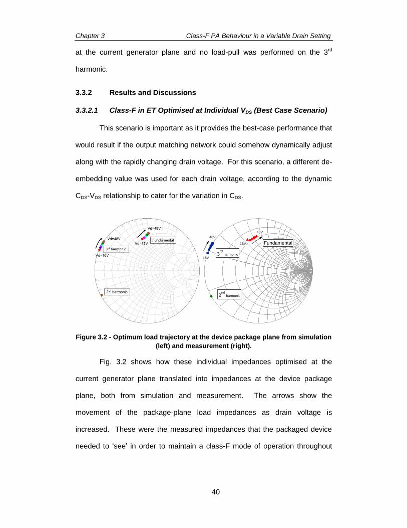
Chapter 3 Class-F PA Behaviour in a Variable Drain Setting
40
at the current generator plane and no load-pull was performed on the 3rd
harmonic.
3.3.2 Results and Discussions
3.3.2.1 Class-F in ET Optimised at Individual VDS (Best Case Scenario)
This scenario is important as it provides the best-case performance that
would result if the output matching network could somehow dynamically adjust
along with the rapidly changing drain voltage. For this scenario, a different de-
embedding value was used for each drain voltage, according to the dynamic
CDS-VDS relationship to cater for the variation in CDS.
Figure 3.2 - Optimum load trajectory at the device package plane from simulation
(left) and measurement (right).
Fig. 3.2 shows how these individual impedances optimised at the
current generator plane translated into impedances at the device package
plane, both from simulation and measurement. The arrows show the
movement of the package-plane load impedances as drain voltage is
increased. These were the measured impedances that the packaged device
needed to ‘see’ in order to maintain a class-F mode of operation throughout
-1.0
-0.5
0.0
0.5
1.0
-1.0 -0.5 0.0 0.5 1.0
Fundamental
2nd
harmonic
3rd
harmonic
16V
48V
16V
48V

Chapter 3 Class-F PA Behaviour in a Variable Drain Setting
41
the ET range. This is useful as it gives a measure of the magnitude of change
required when optimising for different modulation schemes for example.
The load-pull grid resolution used in measurements and simulation
limited the accuracy of the optimum load locations; however the Smith charts
present the trend of the load trajectory at the package plane. There were 2
factors that affected the shift of the optimum fundamental load. On the current
generator plane, the optimum fundamental real impedance increased with
drain bias, since the quiescent point on the I-V plane moved further away from
the knee region and the slope of the dynamic load line became lower (more
negative) to maintain high efficiency. At the same time, the nonlinear CDS
variation with drain bias presented a reactive impedance shift at different bias
points. This variation effect can also be seen on the 3rd harmonic load
trajectory, which presents an open circuit on the current generator plane at
each bias point. The 2nd harmonic load on the package plane did not change
with drain bias as the 2nd harmonic voltage was shorted at the current
generator plane.
Fig. 3.3 shows the time-domain class-F voltage and current waveforms,
as well as the dynamic load lines at the current generator plane when the
class-F mode was optimised for each value of VDS. The measured drain
current at the device current generator plane swung below zero due to residual
displacement current from the dynamic output capacitance (CDS). This
happened because the static de-embedding parameter used at each VDS was
only appropriate for one particular DC drain voltage, and not the whole voltage
swing. The achieved ‘maximum available efficiency’ and output power are
plotted in Fig. 3.4, where the comparison with other scenarios is shown.

Chapter 3 Class-F PA Behaviour in a Variable Drain Setting
42
Figure 3.3 – Voltage and current waveforms (top) and dynamic load lines
(bottom) of the class-F mode in ET when optimised at each drain bias.
3.3.2.2 Class-F in ET Optimised at 48V and 28V Drain Voltages
These two separate scenarios allow for the estimation of the drain
efficiency degradation that can be expected in a real circuit where the load is
fixed. The optimal fundamental, 2nd harmonic and 3rd harmonic class-F load
impedances were identified at one drain bias (48V or 28V), and then kept
constant while the device was characterised for drain bias points from 16V to
48V in 4V steps.
Optimising the matching network at a peak drain bias of 48V produced
a high peak efficiency of 74% but this rapidly dropped to 64% and 56% at
7.5dB and 9dB OBO, respectively. This can present a significant disadvantage
when used with signals with high peak to average power ratio (PAPR), where
the PA only reaches peak power less than 1% of the time [7].
80
60
40
20Dra
in v
olta
ge
(V
)
2.01.51.00.50.0
Time (ns)
600
400
200
0D
rain
cu
rren
t (mA
)
48V
16V
800
600
400
200
0
Dra
in c
urr
en
t (m
A)
806040200
Drain voltage (V)
48V
16V
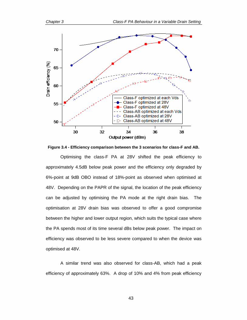
Chapter 3 Class-F PA Behaviour in a Variable Drain Setting
43
Figure 3.4 - Efficiency comparison between the 3 scenarios for class-F and AB.
Optimising the class-F PA at 28V shifted the peak efficiency to
approximately 4.5dB below peak power and the efficiency only degraded by
6%-point at 9dB OBO instead of 18%-point as observed when optimised at
48V. Depending on the PAPR of the signal, the location of the peak efficiency
can be adjusted by optimising the PA mode at the right drain bias. The
optimisation at 28V drain bias was observed to offer a good compromise
between the higher and lower output region, which suits the typical case where
the PA spends most of its time several dBs below peak power. The impact on
efficiency was observed to be less severe compared to when the device was
optimised at 48V.
A similar trend was also observed for class-AB, which had a peak
efficiency of approximately 63%. A drop of 10% and 4% from peak efficiency

Chapter 3 Class-F PA Behaviour in a Variable Drain Setting
44
was observed at 9dB OBO when it was optimised at 48V and 28V,
respectively.
3.4 Analysing the Linearity vs. Efficiency Trade-Off for
Different PA Modes in an ET Architecture
In an ET system, the selection of the drain bias supply for a particular
input envelope voltage is accomplished through the definition of an envelope
shaping function. This shaping function can be formulated for example to
target optimum efficiency by keeping the device in the right compression level
at all times where possible, or it can also be used to target linearity by
maintaining a constant gain [7].
In this section, the linearity versus efficiency trade-off analysis was
performed by examining the effects of these different shaping functions: the
first was the max-PAE shaping function that targets maximum power added
efficiency (PAE) and the second function referred to in this work as the flat-gain
shaping function that targets a constant gain for linearity. The primary
objective of this analysis is to quantify the efficiency trade-off when the max-
PAE shaping function is used in a high-efficiency mode such as class-F.
Waveform engineering was utilised in this analysis, revealing the intrinsic
device behaviour under these different shaping functions in an ET
environment.
The second objective is to relate the findings on the ET shaping
functions for linearity improvement from this work with the previous baseband
injection work in [1, 8-12], and being able to finally understand its impact on
efficiency, which was not analysed before.
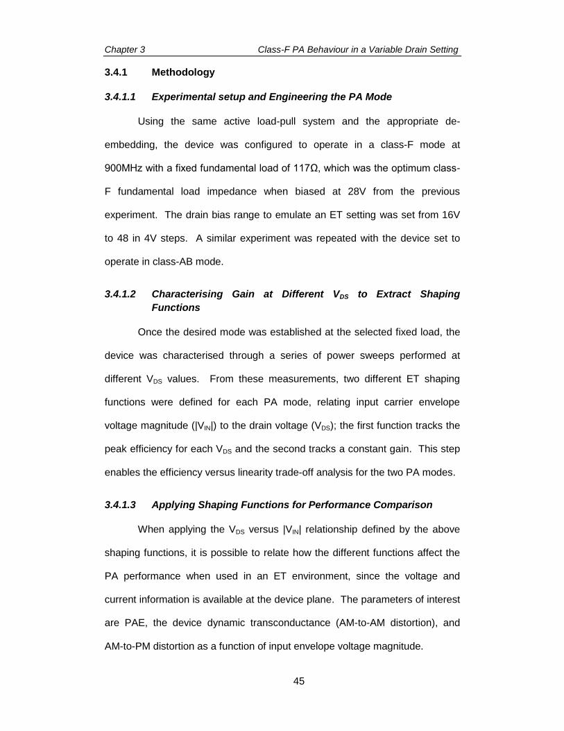
Chapter 3 Class-F PA Behaviour in a Variable Drain Setting
45
3.4.1 Methodology
3.4.1.1 Experimental setup and Engineering the PA Mode
Using the same active load-pull system and the appropriate de-
embedding, the device was configured to operate in a class-F mode at
900MHz with a fixed fundamental load of 117Ω, which was the optimum class-
F fundamental load impedance when biased at 28V from the previous
experiment. The drain bias range to emulate an ET setting was set from 16V
to 48 in 4V steps. A similar experiment was repeated with the device set to
operate in class-AB mode.
3.4.1.2 Characterising Gain at Different VDS to Extract Shaping
Functions
Once the desired mode was established at the selected fixed load, the
device was characterised through a series of power sweeps performed at
different VDS values. From these measurements, two different ET shaping
functions were defined for each PA mode, relating input carrier envelope
voltage magnitude (|VIN|) to the drain voltage (VDS); the first function tracks the
peak efficiency for each VDS and the second tracks a constant gain. This step
enables the efficiency versus linearity trade-off analysis for the two PA modes.
3.4.1.3 Applying Shaping Functions for Performance Comparison
When applying the VDS versus |VIN| relationship defined by the above
shaping functions, it is possible to relate how the different functions affect the
PA performance when used in an ET environment, since the voltage and
current information is available at the device plane. The parameters of interest
are PAE, the device dynamic transconductance (AM-to-AM distortion), and
AM-to-PM distortion as a function of input envelope voltage magnitude.
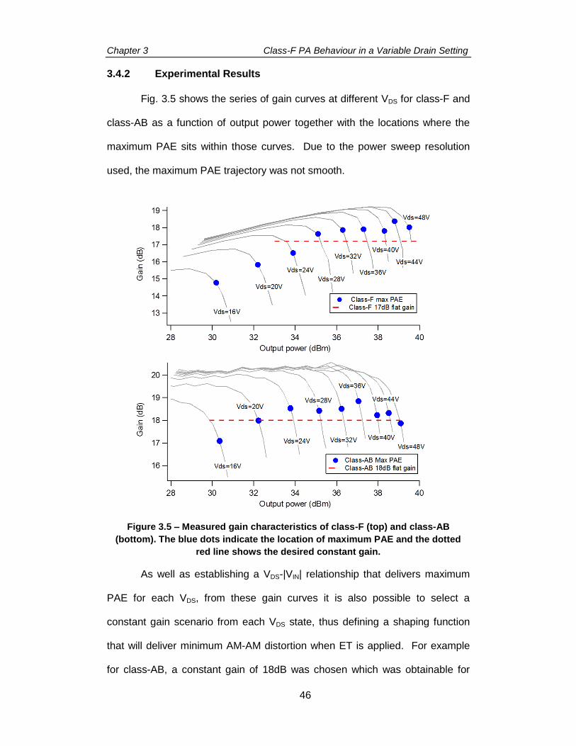
Chapter 3 Class-F PA Behaviour in a Variable Drain Setting
46
3.4.2 Experimental Results
Fig. 3.5 shows the series of gain curves at different VDS for class-F and
class-AB as a function of output power together with the locations where the
maximum PAE sits within those curves. Due to the power sweep resolution
used, the maximum PAE trajectory was not smooth.
Figure 3.5 – Measured gain characteristics of class-F (top) and class-AB
(bottom). The blue dots indicate the location of maximum PAE and the dotted
red line shows the desired constant gain.
As well as establishing a VDS-|VIN| relationship that delivers maximum
PAE for each VDS, from these gain curves it is also possible to select a
constant gain scenario from each VDS state, thus defining a shaping function
that will deliver minimum AM-AM distortion when ET is applied. For example
for class-AB, a constant gain of 18dB was chosen which was obtainable for
Chapter 3 Class-F PA Behaviour in a Variable Drain Setting
47
9dB of the output power range. For class-F, due to the gain expansion-
compression characteristic, a constant gain of 17dB was selected, which was
obtainable for 6dB of the dynamic range from peak power. The resulting ‘max-
PAE’ and ‘flat-gain’ shaping functions that described the relationship between
the required drain supply voltage and the magnitude of the input envelope
voltage (|VIN|) for class-F and class-AB modes are shown in Fig. 3.6.
Figure 3.6 – Extracted shaping functions for efficiency (blue) and linearity (red)
for class-F (top) and class-AB (bottom).
For both PA modes, the ‘flat-gain’ shaping function has a quadratic
relationship with the input envelope voltage, consisting of second-order
polynomial terms. While this behaviour was extracted from a set of CW power

Chapter 3 Class-F PA Behaviour in a Variable Drain Setting
48
sweeps this result is consistent with experimental dynamic observations with
complex modulation presented in the baseband injection work in [1] where the
baseband signal consisting of even order terms, when injected at the drain
minimized AM-AM distortion. This was due to the mixing process between the
input RF signal and the injected baseband signal, as the device was constantly
driven into compression throughout the ET range. The ‘max-PAE’ scenario on
the other hand appeared to require a linear relationship. In practice a
minimum VDS is set above the knee voltage in the shaping function to avoid
gain collapse at low drive levels [13].
Fig. 3.7 shows the efficiency comparison between ‘flat-gain’ and ‘max-
PAE’ shaping functions, for both modes of amplifier. Since the class-F loads
were optimised when the device was biased at 28V which represented
average power, the resulting overall ET efficiency peaked somewhat in the
middle of the output power range, as expected. Remarkably, for class-F, it can
be seen that the efficiency degraded only by approximately 2% when the ‘flat-
gain’ shaping function was used in place of the ‘max-PAE’ function.
Figure 3.7 – Measured PAE comparison between the 2 shaping functions for
class-F and class-AB.
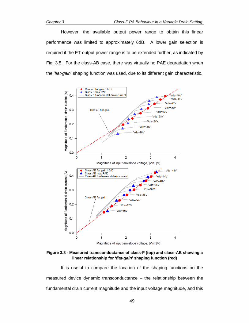
Chapter 3 Class-F PA Behaviour in a Variable Drain Setting
49
However, the available output power range to obtain this linear
performance was limited to approximately 6dB. A lower gain selection is
required if the ET output power range is to be extended further, as indicated by
Fig. 3.5. For the class-AB case, there was virtually no PAE degradation when
the ‘flat-gain’ shaping function was used, due to its different gain characteristic.
Figure 3.8 - Measured transconductance of class-F (top) and class-AB showing a
linear relationship for ‘flat-gain’ shaping function (red)
It is useful to compare the location of the shaping functions on the
measured device dynamic transconductance – the relationship between the
fundamental drain current magnitude and the input voltage magnitude, and this
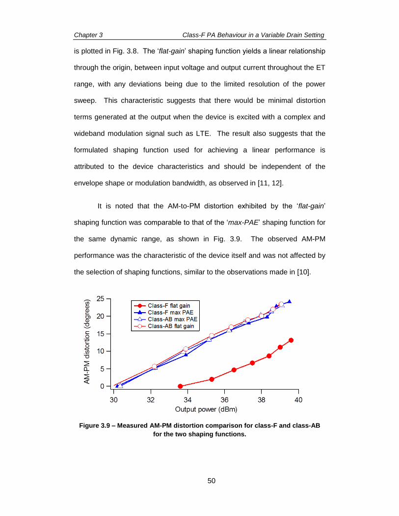
Chapter 3 Class-F PA Behaviour in a Variable Drain Setting
50
is plotted in Fig. 3.8. The ‘flat-gain’ shaping function yields a linear relationship
through the origin, between input voltage and output current throughout the ET
range, with any deviations being due to the limited resolution of the power
sweep. This characteristic suggests that there would be minimal distortion
terms generated at the output when the device is excited with a complex and
wideband modulation signal such as LTE. The result also suggests that the
formulated shaping function used for achieving a linear performance is
attributed to the device characteristics and should be independent of the
envelope shape or modulation bandwidth, as observed in [11, 12].
It is noted that the AM-to-PM distortion exhibited by the ‘flat-gain’
shaping function was comparable to that of the ‘max-PAE’ shaping function for
the same dynamic range, as shown in Fig. 3.9. The observed AM-PM
performance was the characteristic of the device itself and was not affected by
the selection of shaping functions, similar to the observations made in [10].
Figure 3.9 – Measured AM-PM distortion comparison for class-F and class-AB
for the two shaping functions.

Chapter 3 Class-F PA Behaviour in a Variable Drain Setting
51
3.4.3 Discussions
The effects of using different shaping functions for maximum PAE and
flat gain have been shown for both class-AB and class-F modes, operating in
an ET environment. Experimental results indicate that there was only a small
efficiency trade-off when the flat-gain shaping function relating drain supply
voltage signal to the input voltage magnitude was used within the compression
region of the LDMOS device. It is noted that while the absolute PAE number
obtained from the max-PAE shaping function in Fig. 3.7 was determined by the
fixed load presented to the device, the efficiency trade-off figure (the difference
between the red and blue curves in Fig. 3.7) would vary with the selection of
the constant gain value used in defining the flat-gain shaping function.
The extracted flat-gain shaping function consisted of only even order
terms and was shown to be effective in linearising the device
transconductance in comparison to the maximum PAE case. These results are
consistent with the experimental work carried out in [1, 10-12], indicating a
possibility of using ET drain bias as a linearising baseband signal without
significantly impacting efficiency.
In using the flat-gain shaping function for class-F, the output power
range where this takes effect is determined by the constant gain value
selected, as shown in Fig. 3.5. The selection of the gain value therefore needs
to consider the signal PAPR. The other ET parameter that is dependent on
this constant gain value is the minimum drain bias in the case of the class-F
mode.

Chapter 3 Class-F PA Behaviour in a Variable Drain Setting
52
Also, if the signal PAPR is known, the selection of the constant gain
value for the flat-gain shaping function can be made to coincide with the gain
value which has the maximum PAE at average power. This will increase the
likelihood of attaining the highest possible average efficiency performance
under the constraint of the using a shaping function that targets linearity.
The absolute maximum output power is determined by the fundamental
load impedance selection. This output power requirement may well be a
design constraint that will limit overall efficiency performance. It is noted that
the optimum load for output power at maximum drain bias point is different
from the optimum load for efficiency for the same drain bias. However in ET
the optimum efficiency load is targeted at average power which sits at a lower
drain bias. This reduces the trade-off between maximum output power and
efficiency at the ET system level.
3.5 Relating the ET Linearity Improvement Results with
Previous Baseband Injection Work
Before concluding this chapter, the experimental results of the flat-gain
shaping function for linearity improvement are now compared to the baseband
injection method to understand their correlations, the effectiveness of utilising
ET’s modulated drain bias as a baseband linearisation signal, and the effect of
baseband injection on efficiency, which was not previously analysed.
The previous baseband injection works in [1, 10-12] formulated the
baseband signal in the envelope domain and applied it to the drain of a device.
The device operated in a class-AB mode with a fixed drain bias under
modulated excitations using discrete tones. The output of the device package

Chapter 3 Class-F PA Behaviour in a Variable Drain Setting
53
plane was terminated into 50Ω and was not presented with an optimum load
for efficiency. With the device driven 1.5dB into compression, the baseband
formulation algorithm iteratively calculates the 2nd and 4th order coefficients of
the baseband signal to linearise the device transconductance and suppressing
the IM3 and IM5 products. The maximum current (IMAX) and voltage (VMAX)
were kept constant before and after the baseband signal injection because of
the multiple solutions available for the coefficients.
This section tries to replicate that setup in a simulation environment
taking advantage of the excellent device model available in this work that has
been proven to show a good correlation with load-pull results. For this
simulation, a simple second order baseband signal is injected at the drain
while keeping the maximum current (IMAX) and voltage (VMAX) constant. The
ability to present optimum loads and calculate efficiency is now added in
simulation to evaluate the impact of baseband injection on efficiency. The
transfer function of drain current versus input voltage is also extracted for
comparison with the ET shaping function.
3.5.1 Simulation Setup: Baseband Injection Approach for PA
Linearisation
For this analysis, an Envelope simulation in ADS was used and a two-
tone signal was used for the input as it would enable the baseband signal to be
formulated using a simple sine wave with certain amplitude and phase
combination. Fig. 3.10 shows the schematic of the setup.
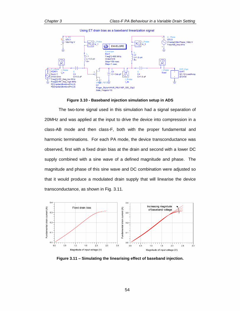
Chapter 3 Class-F PA Behaviour in a Variable Drain Setting
54
Figure 3.10 - Baseband injection simulation setup in ADS
The two-tone signal used in this simulation had a signal separation of
20MHz and was applied at the input to drive the device into compression in a
class-AB mode and then class-F, both with the proper fundamental and
harmonic terminations. For each PA mode, the device transconductance was
observed, first with a fixed drain bias at the drain and second with a lower DC
supply combined with a sine wave of a defined magnitude and phase. The
magnitude and phase of this sine wave and DC combination were adjusted so
that it would produce a modulated drain supply that will linearise the device
transconductance, as shown in Fig. 3.11.
Figure 3.11 – Simulating the linearising effect of baseband injection.

Chapter 3 Class-F PA Behaviour in a Variable Drain Setting
55
3.5.2 Baseband Injection Simulation Results: Class-AB
Fig. 3.12 shows simulation results before and after applying the
baseband injection on a class-AB mode PA while keeping IMAX and VMAX
constant, as well as the resulting VDS-|VIN| relationship. The resulting
transconductance was more linear after injecting the baseband although some
weakly nonlinear effect was still visible since only a second order baseband
signal was applied. The injected baseband transfer function is shown on the
right plot in Fig. 3.12, where it resembled the ET shaping function that targets a
constant gain from Fig. 3.6.
Figure 3.12 - The comparison before (blue) and after (red) baseband injection on
class-AB simulated transconductance (left) and drain bias (right).
The simulated efficiency and intermodulation products are shown in
Table 3.1. Although in this case the maximum PAE was the same as with fixed
bias, the average PAE did improve with the baseband injection, in this example
by almost 6%. The IM3 products in this example were suppressed by 7dB
relative to fixed bias to be around -30dBc and this number can be further
improved with higher order coefficients. As a point of reference, the measured
baseband injection work in [12] achieved -40dBc on a GaN device with a 4th
order baseband signal coefficient for a 3-tone 20MHz signal bandwidth, and it
was noted in [10] that the method was more effective on a GaN device
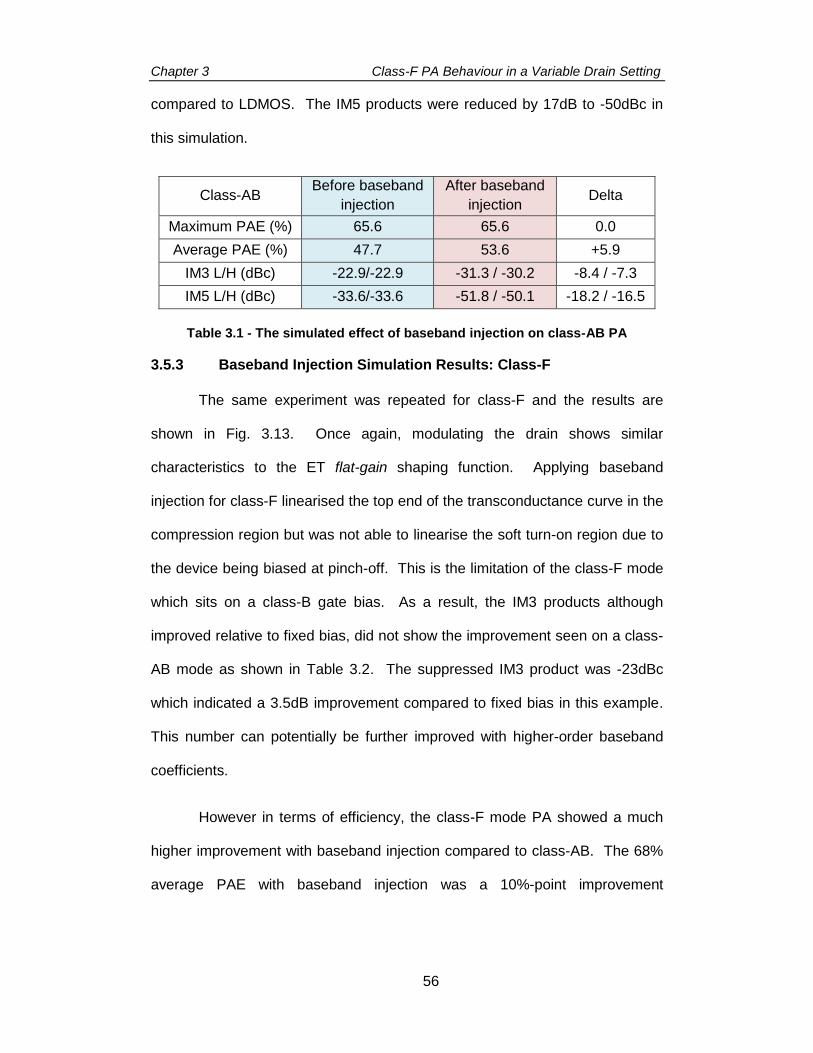
Chapter 3 Class-F PA Behaviour in a Variable Drain Setting
56
compared to LDMOS. The IM5 products were reduced by 17dB to -50dBc in
this simulation.
Class-AB Before baseband
injection
After baseband
injection Delta
Maximum PAE (%) 65.6 65.6 0.0
Average PAE (%) 47.7 53.6 +5.9
IM3 L/H (dBc) -22.9/-22.9 -31.3 / -30.2 -8.4 / -7.3
IM5 L/H (dBc) -33.6/-33.6 -51.8 / -50.1 -18.2 / -16.5
Table 3.1 - The simulated effect of baseband injection on class-AB PA
3.5.3 Baseband Injection Simulation Results: Class-F
The same experiment was repeated for class-F and the results are
shown in Fig. 3.13. Once again, modulating the drain shows similar
characteristics to the ET flat-gain shaping function. Applying baseband
injection for class-F linearised the top end of the transconductance curve in the
compression region but was not able to linearise the soft turn-on region due to
the device being biased at pinch-off. This is the limitation of the class-F mode
which sits on a class-B gate bias. As a result, the IM3 products although
improved relative to fixed bias, did not show the improvement seen on a class-
AB mode as shown in Table 3.2. The suppressed IM3 product was -23dBc
which indicated a 3.5dB improvement compared to fixed bias in this example.
This number can potentially be further improved with higher-order baseband
coefficients.
However in terms of efficiency, the class-F mode PA showed a much
higher improvement with baseband injection compared to class-AB. The 68%
average PAE with baseband injection was a 10%-point improvement
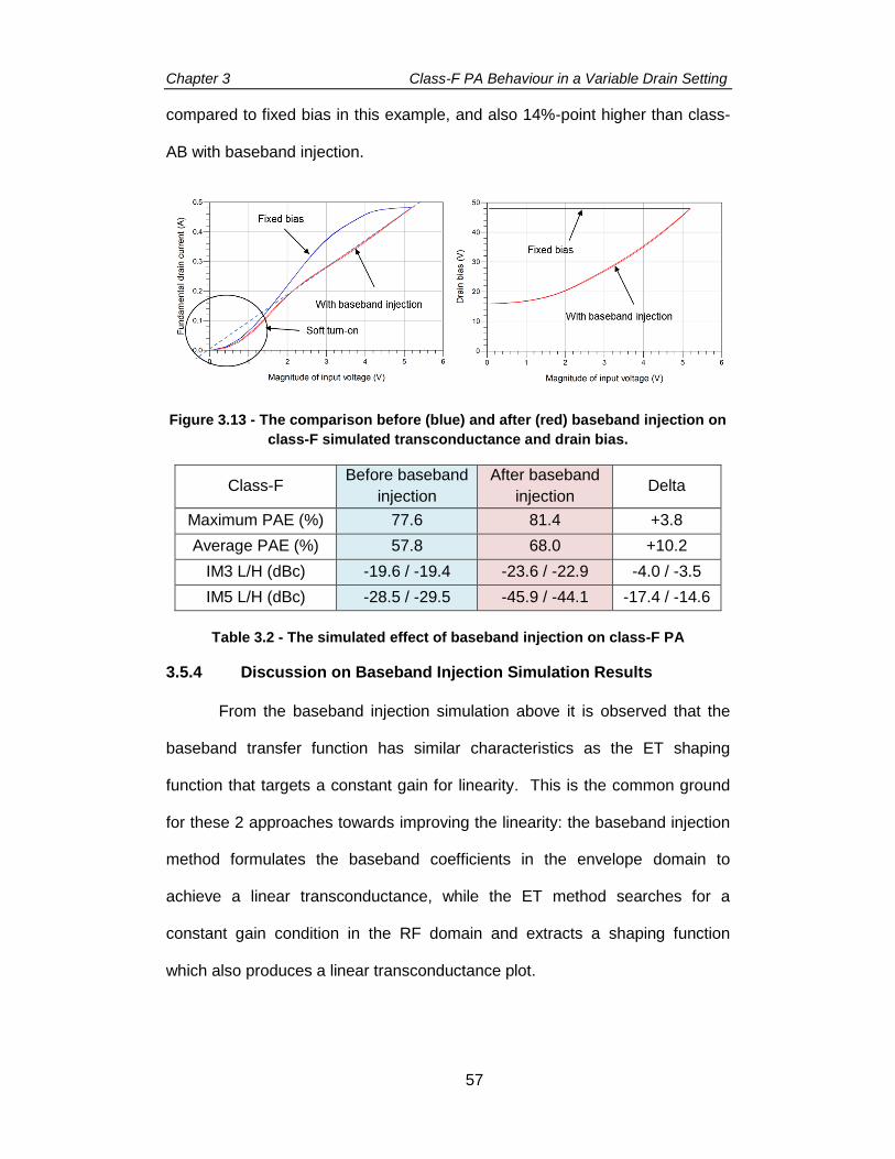
Chapter 3 Class-F PA Behaviour in a Variable Drain Setting
57
compared to fixed bias in this example, and also 14%-point higher than class-
AB with baseband injection.
Figure 3.13 - The comparison before (blue) and after (red) baseband injection on
class-F simulated transconductance and drain bias.
Class-F Before baseband
injection
After baseband
injection Delta
Maximum PAE (%) 77.6 81.4 +3.8
Average PAE (%) 57.8 68.0 +10.2
IM3 L/H (dBc) -19.6 / -19.4 -23.6 / -22.9 -4.0 / -3.5
IM5 L/H (dBc) -28.5 / -29.5 -45.9 / -44.1 -17.4 / -14.6
Table 3.2 - The simulated effect of baseband injection on class-F PA
3.5.4 Discussion on Baseband Injection Simulation Results
From the baseband injection simulation above it is observed that the
baseband transfer function has similar characteristics as the ET shaping
function that targets a constant gain for linearity. This is the common ground
for these 2 approaches towards improving the linearity: the baseband injection
method formulates the baseband coefficients in the envelope domain to
achieve a linear transconductance, while the ET method searches for a
constant gain condition in the RF domain and extracts a shaping function
which also produces a linear transconductance plot.

Chapter 3 Class-F PA Behaviour in a Variable Drain Setting
58
Another key observation is that both approaches improve the average
efficiency of the class-AB and class-F PA compared to fixed drain bias while
achieving a relatively linear performance. This highlights an opportunity of
using the ET architecture to inject linearising baseband signals at the drain
supply to offer some degree of ‘linearisability’ advantage without trading-off
significant efficiency performance.
While class-F exhibits a much higher efficiency compared to class-AB,
its linearity improvement is relatively smaller compared to that of class-AB due
to the soft turn-on at low input voltage as a result of biasing the gate at pinch-
off. Both the ET flat-gain shaping function and baseband injection were only
able linearise the top part of the transconductance curve that is nonlinear due
to compression, but not able to correct for the nonlinearities at the turn-on
region. This presents limitation for a class-F linearity performance when
implemented with baseband injection, and more importantly with a linearising
ET shaping function. This limitation will be discussed in Chapter 5 where a
class-F PA is designed, fabricated, and tested in an ET system.
3.6 Conclusions
Using waveform engineering, the behaviour of a class-F mode PA in a
variable drain setting has been shown in terms of efficiency performance and
optimum load trajectory. It has been observed that the device’s CDS value
affects the efficiency performance of class-F in an ET environment by as much
as 18%-point at 9dB OBO as it shifts the optimum fundamental and harmonic
loads at different drain bias settings. To reduce the efficiency degradation, the
class-F PA needs to be optimised at the average voltage, depending on the

Chapter 3 Class-F PA Behaviour in a Variable Drain Setting
59
signal PAPR. However this may prove to be a challenge in terms of producing
the required output power. This challenge will be analysed in the next chapter,
in formulating an optimum design flow for ET applications.
It was also concluded that the device model used in this work has a
good correlation with the actual device in terms of measurements at the current
generator plane. This provides a significant advantage in the next steps of
research presented in the following chapters where experiments are carried
out in simulations with high confidence and load-pull measurements are used
primarily as a validation step.
This chapter also described how different shaping functions affect the
linearity and efficiency performance of class-AB and class-F mode power
amplifiers. It was shown that there is minimal trade-off in efficiency when the
shaping function used targets a constant gain, or linear performance, both for
class-AB and class-F as long as the PA is in compression.
It was observed that an ET shaping function that targets a constant
gain performance has a quadratic relationship between the supplied drain
voltage and the magnitude of the input envelope voltage, while a shaping
function that targets maximum efficiency has a linear relationship between
these parameters. This observation agrees with previous work in [1, 10-12]
that an even-order baseband signal can be formulated to linearise and
suppress IM3 and IM5 signals of a PA operating in a class-AB bias. However
it is suspected that the linearisation achieved from the shaping function is
limited in class-F, due to the soft turn-on region at the lower part of the
dynamic range.
Chapter 3 Class-F PA Behaviour in a Variable Drain Setting
60
In the next chapter a systematic method to optimise the RF PA design
for ET is formulated using waveform engineering and a class-F PA design and
fabrication is presented.
3.7 References
[1] F. L. Ogboi, P. J. Tasker, M. Akmal, J. Lees, J. Benedikt, S. Bensmida, et al., "A LSNA configured to perform baseband engineering for device linearity investigations under modulated excitations," in Microwave Conference (EuMC), 2013 European, 2013, pp. 684-687.
[2] K. Bumman, M. Junghwan, and K. Ildu, "Efficiently Amplified," Microwave Magazine, IEEE, vol. 11, pp. 87-100, 2010.
[3] P. J. Tasker, "Practical waveform engineering," Microwave Magazine, IEEE, vol. 10, pp. 65-76, 2009.
[4] P. J. Tasker and J. Benedikt, "Waveform Inspired Models and the Harmonic Balance Emulator," Microwave Magazine, IEEE, vol. 12, pp. 38-54, 2011.
[5] K. Joon Hyung, J. Gweon Do, O. Jung Hoon, K. Young Hoon, L. Kwang Chun, J. Jae Ho, et al., "High-Efficiency Envelope-Tracking Transmitter With Optimized Class-F-1 Amplifier and 2-bit Envelope Amplifier for 3G LTE Base Station," Microwave Theory and Techniques, IEEE Transactions on, vol. 59, pp. 1610-1621, 2011.
[6] M. S. Alavi, F. van Rijs, M. Marchetti, M. Squillante, T. Zhang, S. J. Theeuwen, et al., "Efficient LDMOS device operation for envelope tracking amplifiers through second harmonic manipulation," in Microwave Symposium Digest (MTT), 2011 IEEE MTT-S International, 2011, pp. 1-1.
[7] Z. Wang, Envelope Tracking Power Amplifiers for Wireless Communications: Artech House, 2014.
[8] M. Akmal, V. Carrubba, J. Lees, S. Bensmida, J. Benedikt, K. Morris, et al., "Linearity enhancement of GaN HEMTs under complex modulated excitation by optimizing the baseband impedance environment," in Microwave Symposium Digest (MTT), 2011 IEEE MTT-S International, 2011, pp. 1-4.
[9] J. Lees, M. Akmal, S. Bensmida, S. Woodington, S. Cripps, J. Benedikt, et al., "Waveform engineering applied to linear-efficient PA design," in Wireless and Microwave Technology Conference (WAMICON), 2010 IEEE 11th Annual, 2010, pp. 1-5.
Chapter 3 Class-F PA Behaviour in a Variable Drain Setting
61
[10] F. L. Ogboi, P. Tasker, Z. Mohkti, J. Lees, J. Benedikt, S. Bensmida, et al., "Sensitivity of AM/AM linearizer to AM/PM distortion in devices," in Microwave Measurement Conference (ARFTG), 2014 83rd ARFTG, 2014, pp. 1-4.
[11] F. L. Ogboi, P. J. Tasker, M. Akmal, J. Lees, J. Benedikt, S. Bensmida, et al., "Investigation of Various Envelope Complexity Linearity under Modulated Stimulus Using a New Envelope Formulation Approach," in Compound Semiconductor Integrated Circuit Symposium (CSICs), 2014 IEEE, 2014, pp. 1-4.
[12] F. L. Ogboi, P. J. Tasker, M. Akmal, J. Lees, J. Benedikt, S. Bensmida, et al., "High bandwidth investigations of a baseband linearization approach formulated in the envelope domain under modulated stimulus," in Microwave Conference (EuMC), 2014 44th European, 2014, pp. 1305-1308.
[13] K. Bumman, K. Jungjoon, K. Dongsu, S. Junghwan, C. Yunsung, K. Jooseung, et al., "Push the Envelope: Design Concepts for Envelope-Tracking Power Amplifiers," Microwave Magazine, IEEE, vol. 14, pp. 68-81, 2013.
Chapter 4 Using Waveform Engineering to Optimise PA Design for ET Applications
62
Chapter 4
Using Waveform Engineering to
Optimise PA Design for
Envelope Tracking Applications
4.1 Introduction
In the previous chapter, the waveform engineering approach was used
to understand the behaviour of a class-F PA in a variable drain voltage setting.
The effect of optimising the load terminations at different bias points has been
demonstrated and the linearity-efficiency trade-off of class-F and class-AB
PA’s was described for different shaping functions. The efficiency of the RF PA
in an ET system determines the highest achievable efficiency of the transmitter
[1]. Additionally, ET has the potential to linearise highly efficient but nonlinear
RF PA’s, with carefully designed shaping functions [2].
The objective of this chapter is to formulate an optimum PA design
methodology for ET applications using waveform engineering, which takes into
account efficiency, linearity, output power, and signal PAPR aspects through
suitable load conditions and shaping function definitions. Subsequently, this
method is then used to design a 10W RF PA using an LDMOS device from
Freescale for an ET application towards the end of this chapter.
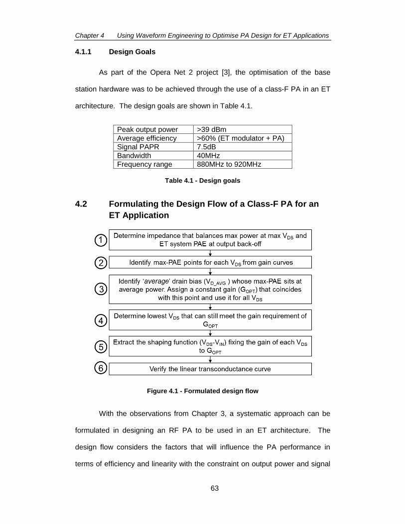
Chapter 4 Using Waveform Engineering to Optimise PA Design for ET Applications
63
4.1.1 Design Goals
As part of the Opera Net 2 project [3], the optimisation of the base
station hardware was to be achieved through the use of a class-F PA in an ET
architecture. The design goals are shown in Table 4.1.
Peak output power >39 dBm
Average efficiency >60% (ET modulator + PA)
Signal PAPR 7.5dB
Bandwidth 40MHz
Frequency range 880MHz to 920MHz
Table 4.1 - Design goals
4.2 Formulating the Design Flow of a Class-F PA for an
ET Application
Figure 4.1 - Formulated design flow
With the observations from Chapter 3, a systematic approach can be
formulated in designing an RF PA to be used in an ET architecture. The
design flow considers the factors that will influence the PA performance in
terms of efficiency and linearity with the constraint on output power and signal

Chapter 4 Using Waveform Engineering to Optimise PA Design for ET Applications
64
PAPR. This is to be achieved through the design of an optimised output
matching circuit based on an assumed signal PAPR and through the
formulation of a shaping function that targets a constant gain performance.
Fig. 4.1 shows the proposed design flow of the PA, achieved through
waveform engineering.
This section describes the design flow together with measurement
results of a class-F PA to be used in an ET system. The useable drain bias
range for ET is from 16V to 48V to avoid the knee and breakdown regions.
4.2.1 Finding the Optimum Fundamental Load
The first step is to find the optimum fundamental load for the output
matching circuit. This selection is a critical step as it determines the maximum
achievable efficiency and maximum output power, as described in Chapter 3.
Since this is fixed throughout the operation of the PA and the device CDS will
shift the optimum fundamental load at different drain bias, a compromise
between maximum output power at 48V bias, and efficiency with ET at
average power is needed.
The optimum fundamental impedance (ROPT) is determined by
performing a load sweep at the maximum drain bias of 48V. To aid the
process, an ET simulation template in ADS is developed to run a 3-dimension
sweep: fundamental real load, drain bias, and input power. The 3dB-
compression output power at peak VDS of 48V and the ET efficiency at 7.5dB
OBO are recorded. The ET efficiency is defined as the trajectory of maximum
PAE curves of different drain bias within the ET drain supply range of 16V to
48V.
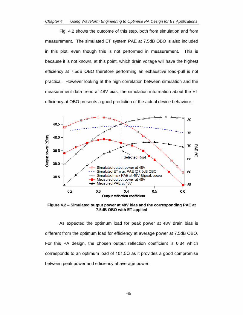
Chapter 4 Using Waveform Engineering to Optimise PA Design for ET Applications
65
Fig. 4.2 shows the outcome of this step, both from simulation and from
measurement. The simulated ET system PAE at 7.5dB OBO is also included
in this plot, even though this is not performed in measurement. This is
because it is not known, at this point, which drain voltage will have the highest
efficiency at 7.5dB OBO therefore performing an exhaustive load-pull is not
practical. However looking at the high correlation between simulation and the
measurement data trend at 48V bias, the simulation information about the ET
efficiency at OBO presents a good prediction of the actual device behaviour.
Figure 4.2 – Simulated output power at 48V bias and the corresponding PAE at 7.5dB OBO with ET applied
As expected the optimum load for peak power at 48V drain bias is
different from the optimum load for efficiency at average power at 7.5dB OBO.
For this PA design, the chosen output reflection coefficient is 0.34 which
corresponds to an optimum load of 101.5Ω as it provides a good compromise
between peak power and efficiency at average power.

Chapter 4 Using Waveform Engineering to Optimise PA Design for ET Applications
66
4.2.2 Identifying Maximum-PAE locations, Assigning Constant Gain
(GOPT), and Minimum Drain Bias (VD_MIN) from Gain Curves
The next step is to obtain the device gain characteristics when
presented with the selected fundamental load at the current generator plane,
for different drain bias points. A family of gain curves is obtained from power
sweeps at different drain bias points with the device operating in a class-F
mode, as shown in Fig. 4.3.
For each drain bias point, the point of maximum PAE is identified. The
drain bias point that has its maximum PAE closest to the average power in this
case is 20V, and the intersecting gain of 15.4dB is chosen as the target
constant gain value (GOPT) for each VDS. The lowest drain bias (VD_MIN) that
can still provide this target gain value is 16V. This value is set as the minimum
for the ET drain supply range.
The measured PAE, also shown in Fig. 4.3, indicates a 3% worst-case
degradation in efficiency when the ET shaping function for constant gain is
used, while the output power range where this constant gain can be achieved
is approximately 10dB. This small trade-off in efficiency agrees with the
measured results from Fig. 3.7 in Chapter 3, even though a different load
(117Ω) is used. This indicates, potentially, that ET can provide both efficiency
and linearity improvements simultaneously.
The maximum output power was measured to be 39.6dBm at 48V drain
bias. With a PAPR of 7.5dB, the average power is estimated to be 32dBm.
The measured PAE at average power is 67% when the drain is biased at 20V.
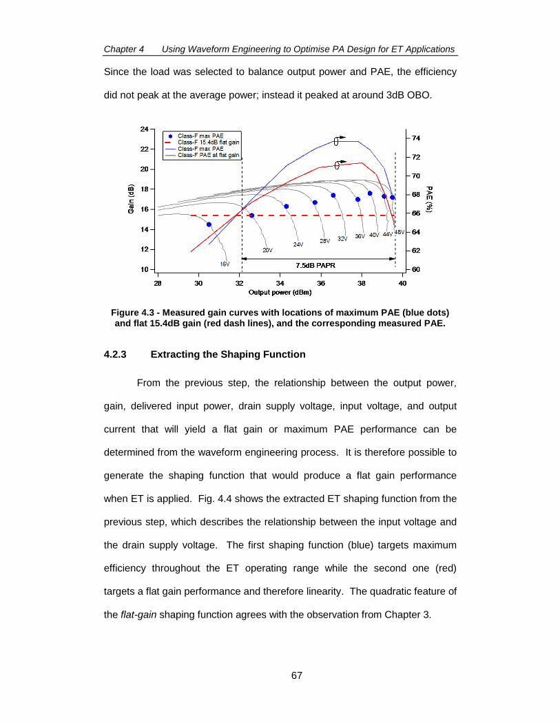
Chapter 4 Using Waveform Engineering to Optimise PA Design for ET Applications
67
Since the load was selected to balance output power and PAE, the efficiency
did not peak at the average power; instead it peaked at around 3dB OBO.
Figure 4.3 - Measured gain curves with locations of maximum PAE (blue dots) and flat 15.4dB gain (red dash lines), and the corresponding measured PAE.
4.2.3 Extracting the Shaping Function
From the previous step, the relationship between the output power,
gain, delivered input power, drain supply voltage, input voltage, and output
current that will yield a flat gain or maximum PAE performance can be
determined from the waveform engineering process. It is therefore possible to
generate the shaping function that would produce a flat gain performance
when ET is applied. Fig. 4.4 shows the extracted ET shaping function from the
previous step, which describes the relationship between the input voltage and
the drain supply voltage. The first shaping function (blue) targets maximum
efficiency throughout the ET operating range while the second one (red)
targets a flat gain performance and therefore linearity. The quadratic feature of
the flat-gain shaping function agrees with the observation from Chapter 3.
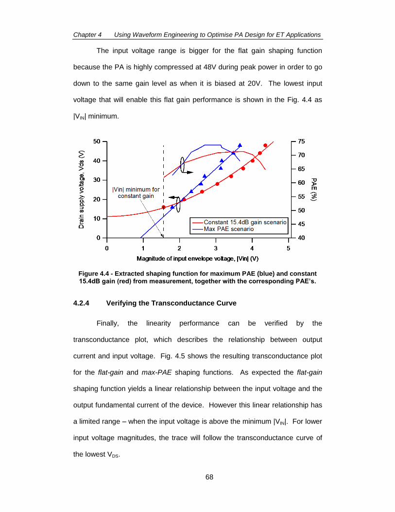
Chapter 4 Using Waveform Engineering to Optimise PA Design for ET Applications
68
The input voltage range is bigger for the flat gain shaping function
because the PA is highly compressed at 48V during peak power in order to go
down to the same gain level as when it is biased at 20V. The lowest input
voltage that will enable this flat gain performance is shown in the Fig. 4.4 as
|VIN| minimum.
Figure 4.4 - Extracted shaping function for maximum PAE (blue) and constant 15.4dB gain (red) from measurement, together with the corresponding PAE’s.
4.2.4 Verifying the Transconductance Curve
Finally, the linearity performance can be verified by the
transconductance plot, which describes the relationship between output
current and input voltage. Fig. 4.5 shows the resulting transconductance plot
for the flat-gain and max-PAE shaping functions. As expected the flat-gain
shaping function yields a linear relationship between the input voltage and the
output fundamental current of the device. However this linear relationship has
a limited range – when the input voltage is above the minimum |VIN|. For lower
input voltage magnitudes, the trace will follow the transconductance curve of
the lowest VDS.
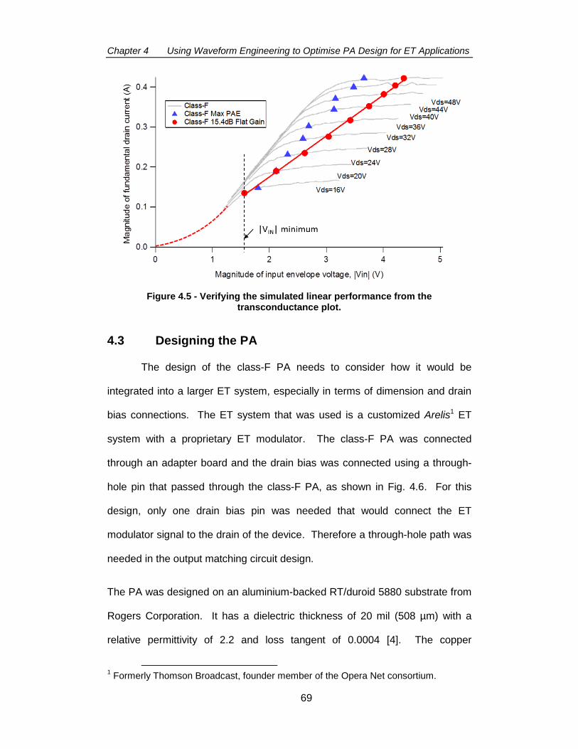
Chapter 4 Using Waveform Engineering to Optimise PA Design for ET Applications
69
Figure 4.5 - Verifying the simulated linear performance from the transconductance plot.
4.3 Designing the PA
The design of the class-F PA needs to consider how it would be
integrated into a larger ET system, especially in terms of dimension and drain
bias connections. The ET system that was used is a customized Arelis1 ET
system with a proprietary ET modulator. The class-F PA was connected
through an adapter board and the drain bias was connected using a through-
hole pin that passed through the class-F PA, as shown in Fig. 4.6. For this
design, only one drain bias pin was needed that would connect the ET
modulator signal to the drain of the device. Therefore a through-hole path was
needed in the output matching circuit design.
The PA was designed on an aluminium-backed RT/duroid 5880 substrate from
Rogers Corporation. It has a dielectric thickness of 20 mil (508 µm) with a
relative permittivity of 2.2 and loss tangent of 0.0004 [4]. The copper
1 Formerly Thomson Broadcast, founder member of the Opera Net consortium.
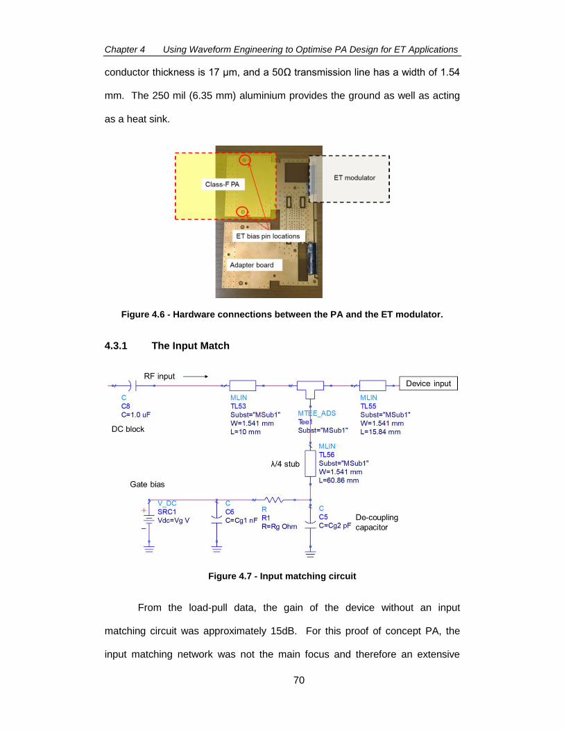
Chapter 4 Using Waveform Engineering to Optimise PA Design for ET Applications
70
conductor thickness is 17 μm, and a 50Ω transmission line has a width of 1.54
mm. The 250 mil (6.35 mm) aluminium provides the ground as well as acting
as a heat sink.
Figure 4.6 - Hardware connections between the PA and the ET modulator.
4.3.1 The Input Match
Figure 4.7 - Input matching circuit
From the load-pull data, the gain of the device without an input
matching circuit was approximately 15dB. For this proof of concept PA, the
input matching network was not the main focus and therefore an extensive
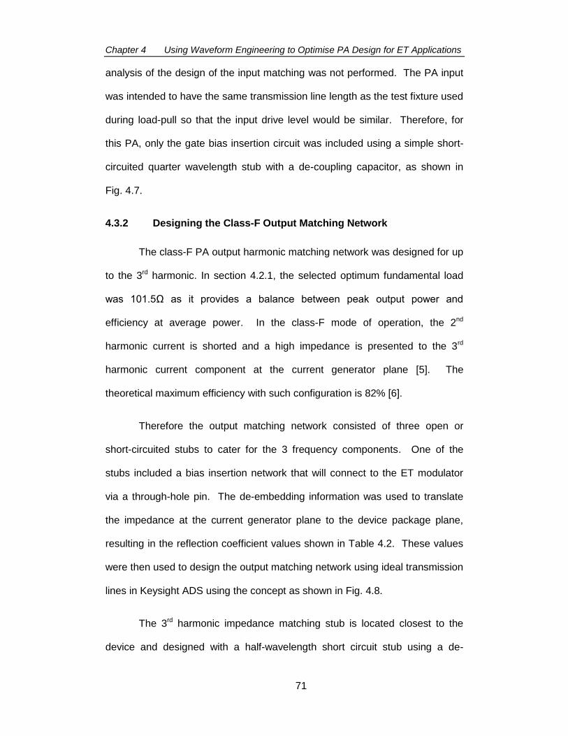
Chapter 4 Using Waveform Engineering to Optimise PA Design for ET Applications
71
analysis of the design of the input matching was not performed. The PA input
was intended to have the same transmission line length as the test fixture used
during load-pull so that the input drive level would be similar. Therefore, for
this PA, only the gate bias insertion circuit was included using a simple short-
circuited quarter wavelength stub with a de-coupling capacitor, as shown in
Fig. 4.7.
4.3.2 Designing the Class-F Output Matching Network
The class-F PA output harmonic matching network was designed for up
to the 3rd harmonic. In section 4.2.1, the selected optimum fundamental load
was 101.5Ω as it provides a balance between peak output power and
efficiency at average power. In the class-F mode of operation, the 2nd
harmonic current is shorted and a high impedance is presented to the 3rd
harmonic current component at the current generator plane [5]. The
theoretical maximum efficiency with such configuration is 82% [6].
Therefore the output matching network consisted of three open or
short-circuited stubs to cater for the 3 frequency components. One of the
stubs included a bias insertion network that will connect to the ET modulator
via a through-hole pin. The de-embedding information was used to translate
the impedance at the current generator plane to the device package plane,
resulting in the reflection coefficient values shown in Table 4.2. These values
were then used to design the output matching network using ideal transmission
lines in Keysight ADS using the concept as shown in Fig. 4.8.
The 3rd harmonic impedance matching stub is located closest to the
device and designed with a half-wavelength short circuit stub using a de-
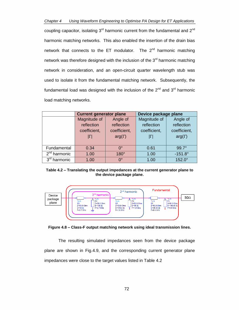
Chapter 4 Using Waveform Engineering to Optimise PA Design for ET Applications
72
coupling capacitor, isolating 3rd harmonic current from the fundamental and 2nd
harmonic matching networks. This also enabled the insertion of the drain bias
network that connects to the ET modulator. The 2nd harmonic matching
network was therefore designed with the inclusion of the 3rd harmonic matching
network in consideration, and an open-circuit quarter wavelength stub was
used to isolate it from the fundamental matching network. Subsequently, the
fundamental load was designed with the inclusion of the 2nd and 3rd harmonic
load matching networks.
Current generator plane Device package plane
Magnitude of
reflection
coefficient,
|Γ|
Angle of
reflection
coefficient,
arg(Γ)
Magnitude of
reflection
coefficient,
|Γ|
Angle of
reflection
coefficient,
arg(Γ)
Fundamental 0.34 0° 0.61 99.7°
2nd harmonic 1.00 180° 1.00 -151.8°
3rd harmonic 1.00 0° 1.00 152.0°
Table 4.2 – Translating the output impedances at the current generator plane to the device package plane.
Figure 4.8 – Class-F output matching network using ideal transmission lines.
The resulting simulated impedances seen from the device package
plane are shown in Fig.4.9, and the corresponding current generator plane
impedances were close to the target values listed in Table 4.2
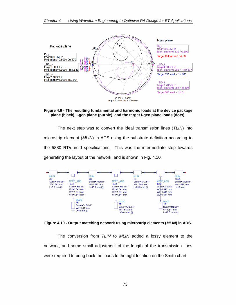
Chapter 4 Using Waveform Engineering to Optimise PA Design for ET Applications
73
Figure 4.9 - The resulting fundamental and harmonic loads at the device package plane (black), I-gen plane (purple), and the target I-gen plane loads (dots).
The next step was to convert the ideal transmission lines (TLIN) into
microstrip element (MLIN) in ADS using the substrate definition according to
the 5880 RT/duroid specifications. This was the intermediate step towards
generating the layout of the network, and is shown in Fig. 4.10.
Figure 4.10 - Output matching network using microstrip elements (MLIN) in ADS.
The conversion from TLIN to MLIN added a lossy element to the
network, and some small adjustment of the length of the transmission lines
were required to bring back the loads to the right location on the Smith chart.
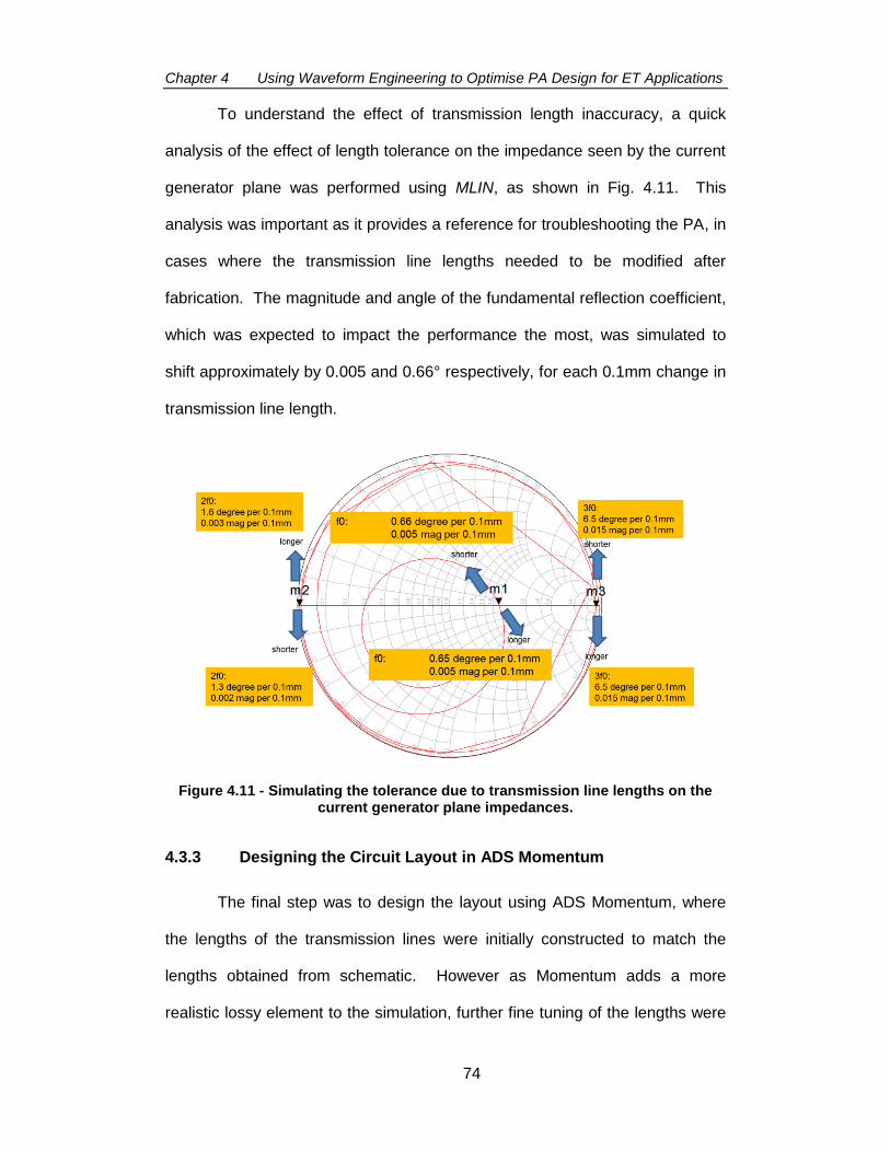
Chapter 4 Using Waveform Engineering to Optimise PA Design for ET Applications
74
To understand the effect of transmission length inaccuracy, a quick
analysis of the effect of length tolerance on the impedance seen by the current
generator plane was performed using MLIN, as shown in Fig. 4.11. This
analysis was important as it provides a reference for troubleshooting the PA, in
cases where the transmission line lengths needed to be modified after
fabrication. The magnitude and angle of the fundamental reflection coefficient,
which was expected to impact the performance the most, was simulated to
shift approximately by 0.005 and 0.66° respectively, for each 0.1mm change in
transmission line length.
Figure 4.11 - Simulating the tolerance due to transmission line lengths on the current generator plane impedances.
4.3.3 Designing the Circuit Layout in ADS Momentum
The final step was to design the layout using ADS Momentum, where
the lengths of the transmission lines were initially constructed to match the
lengths obtained from schematic. However as Momentum adds a more
realistic lossy element to the simulation, further fine tuning of the lengths were
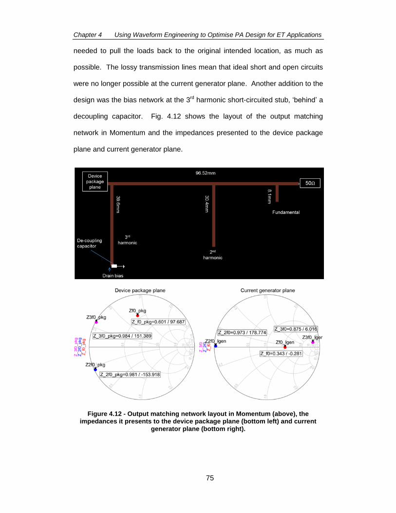
Chapter 4 Using Waveform Engineering to Optimise PA Design for ET Applications
75
needed to pull the loads back to the original intended location, as much as
possible. The lossy transmission lines mean that ideal short and open circuits
were no longer possible at the current generator plane. Another addition to the
design was the bias network at the 3rd harmonic short-circuited stub, ‘behind’ a
decoupling capacitor. Fig. 4.12 shows the layout of the output matching
network in Momentum and the impedances presented to the device package
plane and current generator plane.
Figure 4.12 - Output matching network layout in Momentum (above), the impedances it presents to the device package plane (bottom left) and current
generator plane (bottom right).
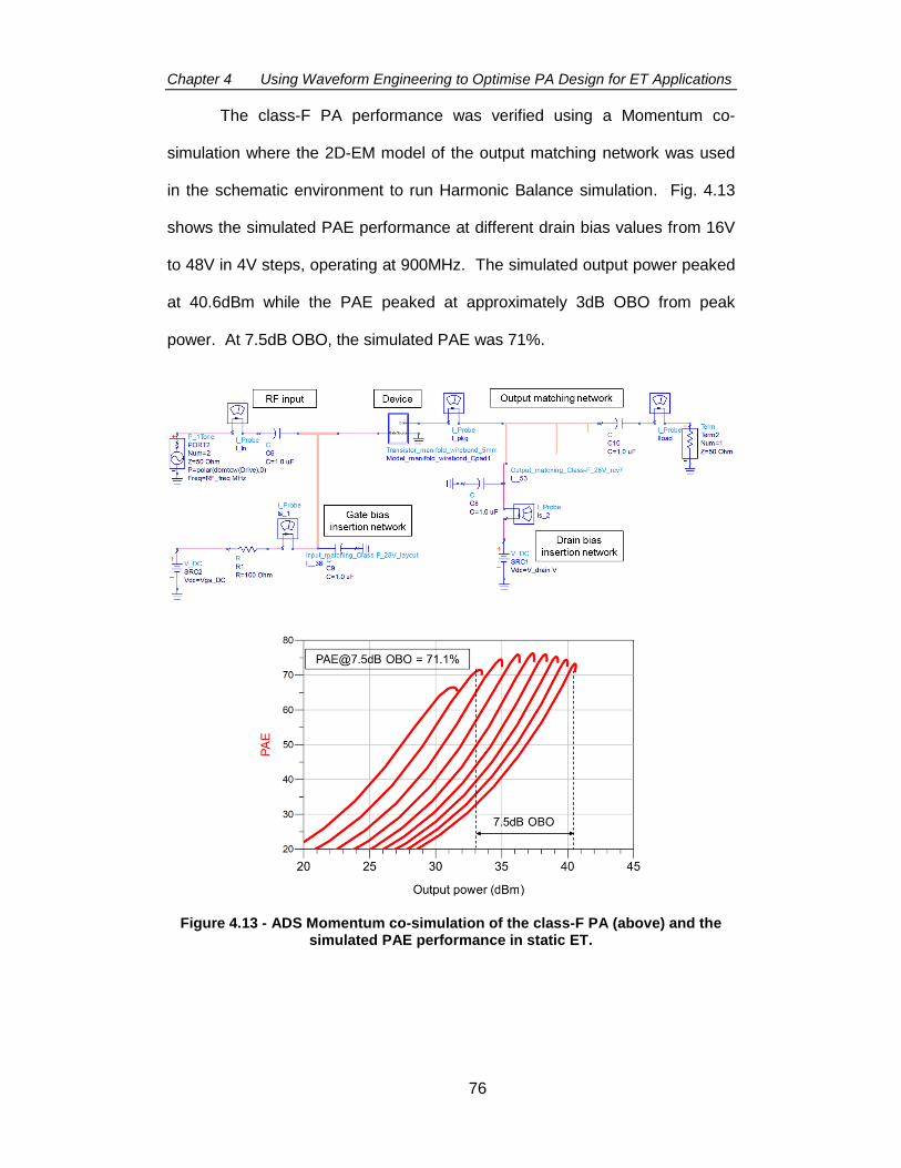
Chapter 4 Using Waveform Engineering to Optimise PA Design for ET Applications
76
The class-F PA performance was verified using a Momentum co-
simulation where the 2D-EM model of the output matching network was used
in the schematic environment to run Harmonic Balance simulation. Fig. 4.13
shows the simulated PAE performance at different drain bias values from 16V
to 48V in 4V steps, operating at 900MHz. The simulated output power peaked
at 40.6dBm while the PAE peaked at approximately 3dB OBO from peak
power. At 7.5dB OBO, the simulated PAE was 71%.
Figure 4.13 - ADS Momentum co-simulation of the class-F PA (above) and the simulated PAE performance in static ET.
Chapter 4 Using Waveform Engineering to Optimise PA Design for ET Applications
77
4.3.4 Completing the Layout
The next addition to the layout was the connection for the drain bias
input via the ET modulator. This was achieved by adding a hole near the 3rd
harmonic matching stub, and following the de-coupling capacitor as shown in
Fig. 4.14. The connection to the ET modulator was done by way of a through-
hole pin that comes from the ET adapter as shown in Fig.4.6. In case the
fundamental and 2nd harmonic open circuit stubs need to be extended after
fabrication, some copper rectangles of the same width as the stubs were
added during fabrication. Additionally, a small series resistor and some low-
frequency filtering capacitors were added to the gate bias network for stability
purpose. The class-F PA was fabricated in-house using a milling machine.
Fig. 4.14 shows the final layout and the fabricated class-F PA.
4.4 Conclusions
Working with modulated signal of a known PAPR, a design method has
been formulated using the waveform engineering approach to achieve an
optimum efficiency-linearity performance of an RF PA for ET applications. The
method utilizes the waveform engineering capability to determine the optimum
load and a linearising shaping function.
The formulated design method has been used to design an actual
class-F PA that will be integrated it into to a real ET system. The PA uses a
10W device from Freescale with a defined ET drain bias range of 16V to 48V.
From simulation the RF PA efficiency at 900MHz at 7.5dB OBO was 71%,
constrained by the output power requirement at peak power, while CW load-
pull measurement data of the device predicted it to be 67%.
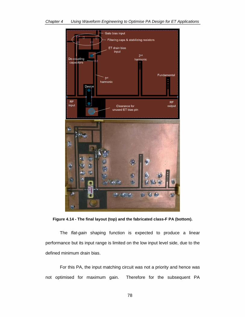
Chapter 4 Using Waveform Engineering to Optimise PA Design for ET Applications
78
Figure 4.14 - The final layout (top) and the fabricated class-F PA (bottom).
The flat-gain shaping function is expected to produce a linear
performance but its input range is limited on the low input level side, due to the
defined minimum drain bias.
For this PA, the input matching circuit was not a priority and hence was
not optimised for maximum gain. Therefore for the subsequent PA

Chapter 4 Using Waveform Engineering to Optimise PA Design for ET Applications
79
performance analysis, the drain efficiency (DE) measurement was used
instead of power-added efficiency (PAE).
In the next chapter, the PA performance is tested as a standalone
amplifier using a CW signal to verify its performance before being paired up
with an ET modulator in a full ET setup for a system level performance test
with an LTE signal of 7.5dB PAPR.
4.5 References
[1] E. McCune, Dynamic Power Supply Transmitters: Cambridge University Press, 2015.
[2] Z. Wang, Envelope Tracking Power Amplifiers for Wireless Communications: Artech House, 2014.
[3] M. Lasanen, M. Aubree, C. Cassan, A. Conte, J. David, S. E. Elayoubi, et al., "Environmental friendly mobile radio networks: Approaches of the European OPERA-Net 2 project," in Telecommunications (ICT), 2013 20th International Conference on, 2013, pp. 1-5.
[4] RT/duroid ® 5870/5880 High Frequency Laminates Datasheet [Online]. Available: http://www.rogerscorp.com/documents/606/acs/RT-duroid-5870-5880-Data-Sheet.pdf
[5] S. C. Cripps, RF Power Amplifiers for Wireless Communications: Artech House, 2006.
[6] F. H. Raab, "Maximum efficiency and output of class-F power amplifiers," IEEE Transactions on Microwave Theory and Techniques, vol. 49, pp. 1162-1166, 2001.

Chapter 5 ET System Level Integration & Testing
80
Chapter 5
Envelope Tracking System Level
Integration and Testing
5.1 Introduction
In the previous chapter, the design flow of an RF PA for ET applications
utilising waveform engineering has been demonstrated. A 10W class-F RF PA
has been fabricated using this formulation.
In this chapter, the test method and results of the fabricated class-F PA
are presented, first as a standalone PA and then integrated into a real ET
system at Arelis, France. Due to the test setup limitation at Arelis, the ET
system level test was performed at 885MHz, which was found to still be within
the capability of the class-F PA. The advantages and limitations of using a
class-F PA in an ET system are explained together with simulation results that
replicate the ET system level test.
5.2 Initial PA Standalone Performance Test
5.2.1 Efficiency & Output Power using CW Signal
The fabricated class-F PA was first tested as a standalone amplifier in a
static-ET setting using a CW signal at 900MHz to verify its performance. For
this CW test the drain was biased through a wire soldered onto the drain bias
terminal and connected to a DC supply. Replicating the static ET procedures

Chapter 5 ET System Level Integration & Testing
81
from the load-pull testing stage, the drain bias was stepped from 16V to 48V in
4V steps and for each drain bias a power sweep was performed. Fig. 5.1
shows the drain efficiency and gain curves for each VDS from 16V to 48V in 4V
steps at 900MHz.
The drain efficiency peaked at 73% at approximately 3dB from peak
power, which was the trend predicted by the ADS Momentum co-simulation in
Fig. 4.13, although the simulated peak efficiency was higher by 3%. At 7.5dB
output back-off the drain efficiency from this CW measurement was 68%. It
was observed that the location of the de-coupling capacitor at the output
matching network along the 3rd harmonic matching stub had a significant
impact on drain efficiency, as this effectively alters the load termination of the
3rd harmonic and the fundamental. This was further confirmed through
Momentum co-simulation where the location of the de-coupling capacitor was
varied by 3mm on the layout and the drain efficiency dropped by approximately
5%-point.
The measured trade-off in efficiency was approximately 2% if the
applied ET shaping function targeted a constant gain operation. This was also
consistent with the load-pull characterisation results in Fig. 4.3. However the
optimum gain value was now lower (14dB) because the input was not properly
matched.
In preparing for the ET system level test, the PA efficiency performance
was also measured at 885MHz. As shown in Fig. 5.1, this caused the peak
efficiency to drop by approximately 2%-point but it also moves the peak
efficiency region much closer to the average power.
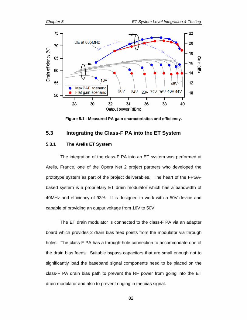
Chapter 5 ET System Level Integration & Testing
82
Figure 5.1 - Measured PA gain characteristics and efficiency.
5.3 Integrating the Class-F PA into the ET System
5.3.1 The Arelis ET System
The integration of the class-F PA into an ET system was performed at
Arelis, France, one of the Opera Net 2 project partners who developed the
prototype system as part of the project deliverables. The heart of the FPGA-
based system is a proprietary ET drain modulator which has a bandwidth of
40MHz and efficiency of 93%. It is designed to work with a 50V device and
capable of providing an output voltage from 16V to 50V.
The ET drain modulator is connected to the class-F PA via an adapter
board which provides 2 drain bias feed points from the modulator via through
holes. The class-F PA has a through-hole connection to accommodate one of
the drain bias feeds. Suitable bypass capacitors that are small enough not to
significantly load the baseband signal components need to be placed on the
class-F PA drain bias path to prevent the RF power from going into the ET
drain modulator and also to prevent ringing in the bias signal.

Chapter 5 ET System Level Integration & Testing
83
The ET system is controlled using software developed by Arelis, which
generates a 5MHz LTE signal from a pseudo-random bit sequence (PRBS)
baseband and has a signal PAPR of 7.5dB. The power level is adjusted using
an intermediate-frequency (IF) gain control panel to ensure the PA reaches a
suitable compression level. The envelope shaping function is entered
manually by the user through a graphical user interface which shows a plot of
the drain supply versus the input envelope, as shown in Fig. 5.2. The interface
allows the user to set 7 points on the graph to alter the shaping function of the
ET modulator. The system also has digital pre-distortion (DPD) capability to
perform nonlinear correction on the PA and improve the adjacent channel
power ratio (ACPR) performance.
Figure 5.2 - ET shaping function entry.
5.3.2 Integrating the Class-F PA into the ET System: Hardware
Connections
The class-F PA was mechanically attached to the ET adapter board to
allow for the drain feed pin to be inserted through the hole that was designed

Chapter 5 ET System Level Integration & Testing
84
for it as previously shown in Fig. 4.14, with an insulating Teflon dielectric to
hold it within. The other end of the adapter board was connected to the ET
drain modulator and the control board. To monitor the modulated ET drain
bias signal, a cable was soldered onto the drain bias feed pin and connected to
an oscilloscope with a series resistor. A second oscilloscope channel was
used to monitor the LTE RF input signal. The gate was biased using a
separate DC power supply. Fig. 5.3 shows the hardware connections to the
class-F PA.
Figure 5.3 – Hardware connections to the class-F PA.
The same Minicircuit ZHL-42 driver amplifier that was used during load-
pull at Cardiff lab was used again in this system to boost the input power. The
output of the class-F PA was connected to a coupler which then terminated
into a 50Ω load. The coupled arm of the coupler was split using a power
splitter and characterised and connected to a spectrum analyser and a power
sensor.
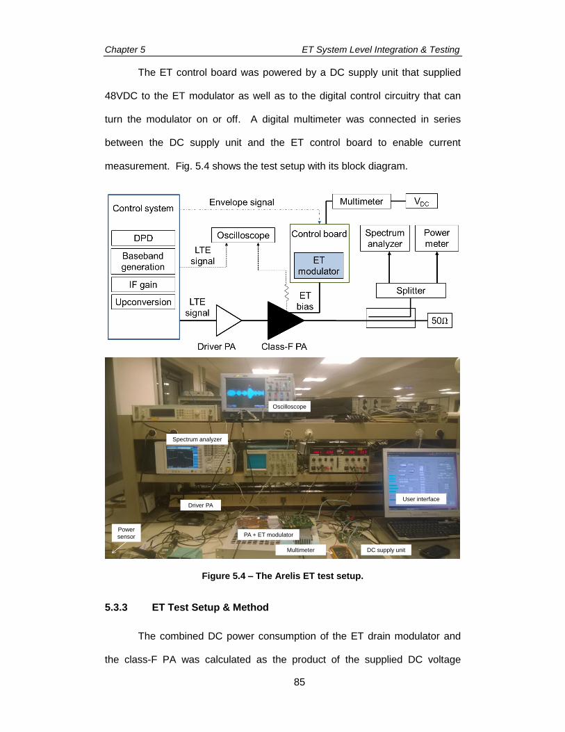
Chapter 5 ET System Level Integration & Testing
85
The ET control board was powered by a DC supply unit that supplied
48VDC to the ET modulator as well as to the digital control circuitry that can
turn the modulator on or off. A digital multimeter was connected in series
between the DC supply unit and the ET control board to enable current
measurement. Fig. 5.4 shows the test setup with its block diagram.
Figure 5.4 – The Arelis ET test setup.
5.3.3 ET Test Setup & Method
The combined DC power consumption of the ET drain modulator and
the class-F PA was calculated as the product of the supplied DC voltage
Oscilloscope
Power
sensor
Spectrum analyzer
PA + ET modulator
DC supply unit
Driver PA
Multimeter
User interface

Chapter 5 ET System Level Integration & Testing
86
(48VDC) and the measured incremental DC current when the ET modulator
was turned on. The power consumption of the control board, which had been
characterised to be 90% efficient, was not taken into account in this case. It
was not possible to measure the efficiency of the class-F PA alone from the
combined efficiency of the ET modulator and the class-F PA, but it can be
estimated since the efficiency of the modulator was previously characterised to
be 93%.
Due to the frequency limitation of the ET system, the centre frequency
of the input signal was limited to 885MHz instead of 900MHz, which was still
within the operating frequency range of the PA, as shown in Fig. 5.1. In fact
with the lower frequency the PA efficiency profile changed such that it peaked
around the average power, but the peak power was now reduced by 0.5dB to
39.2dBm.
The system IF gain was used to adjust the average output power to
approximately 32dBm, which was the estimated average power based on CW
characterisation. The effect of the IF gain adjustment was also characterised
by sweeping its value and observing the effect on efficiency and linearity.
Several changes were made to the shaping function to observe its
effect on the performance. The shaping functions that would replicate the
max-PAE and flat-gain shaping functions were also applied.
The Arelis control software also has the capability to perform nonlinear
correction to provide DPD capability. The non-linear correction was applied in
this measurement to observe the improvement in measured ACPR. The input
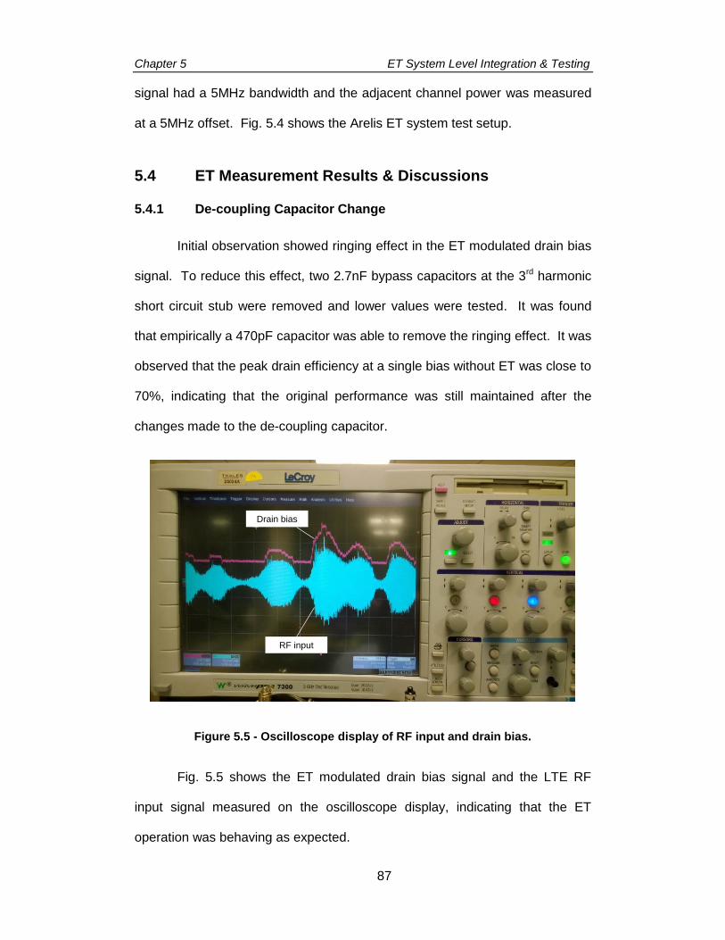
Chapter 5 ET System Level Integration & Testing
87
signal had a 5MHz bandwidth and the adjacent channel power was measured
at a 5MHz offset. Fig. 5.4 shows the Arelis ET system test setup.
5.4 ET Measurement Results & Discussions
5.4.1 De-coupling Capacitor Change
Initial observation showed ringing effect in the ET modulated drain bias
signal. To reduce this effect, two 2.7nF bypass capacitors at the 3rd harmonic
short circuit stub were removed and lower values were tested. It was found
that empirically a 470pF capacitor was able to remove the ringing effect. It was
observed that the peak drain efficiency at a single bias without ET was close to
70%, indicating that the original performance was still maintained after the
changes made to the de-coupling capacitor.
Figure 5.5 - Oscilloscope display of RF input and drain bias.
Fig. 5.5 shows the ET modulated drain bias signal and the LTE RF
input signal measured on the oscilloscope display, indicating that the ET
operation was behaving as expected.
RF input
Drain bias
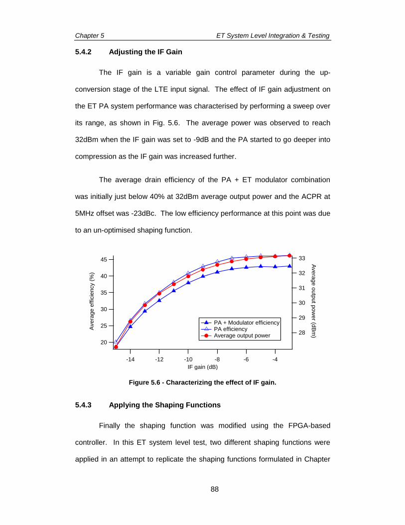
Chapter 5 ET System Level Integration & Testing
88
5.4.2 Adjusting the IF Gain
The IF gain is a variable gain control parameter during the up-
conversion stage of the LTE input signal. The effect of IF gain adjustment on
the ET PA system performance was characterised by performing a sweep over
its range, as shown in Fig. 5.6. The average power was observed to reach
32dBm when the IF gain was set to -9dB and the PA started to go deeper into
compression as the IF gain was increased further.
The average drain efficiency of the PA + ET modulator combination
was initially just below 40% at 32dBm average output power and the ACPR at
5MHz offset was -23dBc. The low efficiency performance at this point was due
to an un-optimised shaping function.
Figure 5.6 - Characterizing the effect of IF gain.
5.4.3 Applying the Shaping Functions
Finally the shaping function was modified using the FPGA-based
controller. In this ET system level test, two different shaping functions were
applied in an attempt to replicate the shaping functions formulated in Chapter
45
40
35
30
25
20
Ave
rag
e e
ffic
iency (
%)
-14 -12 -10 -8 -6 -4
IF gain (dB)
33
32
31
30
29
28
Ave
rag
e o
utp
ut p
ow
er (d
Bm
)
PA + Modulator efficiency PA efficiency Average output power

Chapter 5 ET System Level Integration & Testing
89
3. The minimum drain bias was clipped to 16V as this was the ET modulator
lower limit. However since the shaping function entry works in the digital
domain and uses DAC values, only an estimate of the shaping function was
used (Fig. 5.7). The IF gain was re-adjusted to bring the average power to
approximately 32dBm. Table 5.3 shows the comparison of average drain
efficiency and ACPR results when these 2 shaping functions were used.
The measured average efficiency for the class-F PA + ET modulator
combination was 64% using the max-PAE shaping function. With the
efficiency of the modulator previously characterised to be 93%, the calculated
PA-only average efficiency was 69% which was slightly lower than the
measured efficiency at CW. This is expected and the difference between them
depends on the time-domain profile of the signal. The 64% combined
efficiency obtained with a 10W LDMOS device was relatively high compared to
the work done in [1] where a 10W GaN device operating in ET at 889MHz
achieving 60% drain efficiency when excited using a 5MHz LTE signal with a
6.5dB PAPR.
Average efficiency (PA + ET
Modulator)
Average efficiency (PA only)
Average output power
ACPR @5MHz
offset without DPD
ACPR @5MHz
offset with DPD
Replicating max PAE shaping function
64% 69% 32.2 dBm
-27 dBc -32 dBc
Replicating flat gain shaping function
61% 66% 32.0 dBm
-27 dBc -32 dBc
Table 5.1 - ET performance results.
It was found that using the quadratic-shape shaping function to
replicate the flat-gain shaping function the average efficiency did drop by
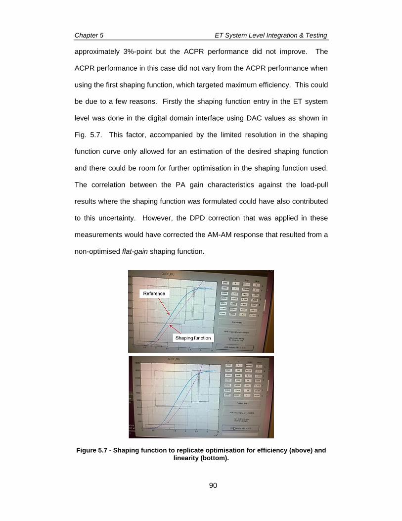
Chapter 5 ET System Level Integration & Testing
90
approximately 3%-point but the ACPR performance did not improve. The
ACPR performance in this case did not vary from the ACPR performance when
using the first shaping function, which targeted maximum efficiency. This could
be due to a few reasons. Firstly the shaping function entry in the ET system
level was done in the digital domain interface using DAC values as shown in
Fig. 5.7. This factor, accompanied by the limited resolution in the shaping
function curve only allowed for an estimation of the desired shaping function
and there could be room for further optimisation in the shaping function used.
The correlation between the PA gain characteristics against the load-pull
results where the shaping function was formulated could have also contributed
to this uncertainty. However, the DPD correction that was applied in these
measurements would have corrected the AM-AM response that resulted from a
non-optimised flat-gain shaping function.
Figure 5.7 - Shaping function to replicate optimisation for efficiency (above) and linearity (bottom).

Chapter 5 ET System Level Integration & Testing
91
The main contributor to the linearity performance in this case was
suspected to be the soft turn-on characteristic of the class-F PA
transconductance as a result of a class-B bias. This effectively means that the
flat-gain shaping function can only linearise the upper half of the output power
range but will not be able to correct for the nonlinearities of the lower half of the
dynamic range, as seen in section 4.2.
The DPD used in this system was designed to work with class-AB type
of amplifiers where they are biased at a distance away from the pinch-off
region, avoiding the nonlinearity from the soft turn-on effect at very low drive
levels. Therefore the use of DPD in this setup was not able to correct for the
nonlinearity at the very low drive level but was more effective at the
compressive region of the transconductance curve at the top end. Fig. 5.8
shows the spectral plot before and after applying the DPD from the Arelis ET
system.
Figure 5.8 - Spectral display of the output signal before (left) and after (right) applying DPD.

Chapter 5 ET System Level Integration & Testing
92
5.5 Verifying the Measured ET Test Results in Simulation
To further verify the ET efficiency and linearity results, an ADS
simulation was established to replicate the ET system level measurements
performed at the Arelis facilities.
5.5.1 CW Simulation to Generate Shaping Functions
Fig. 5.9 shows the CW simulation that was done as part of Chapter 4’s
design flow formulation shown in Appendix B. From this result, 2 shaping
functions were derived: targeting a constant 14.5dB gain (flat-gain) and
maximum efficiency (max-PAE).
Figure 5.9 - CW characterisation to extract ET shaping functions
5.5.2 ET System Simulation Setup
The ET simulation setup, shown in Fig. 5.10 is a modified version of the
Keysight template and uses an Envelope simulation controller and ideal
symbolically-defined devices (SDDs) for the ET modulator. Only the efficiency
of the RF PA is considered while the ET modulator is considered ideal.
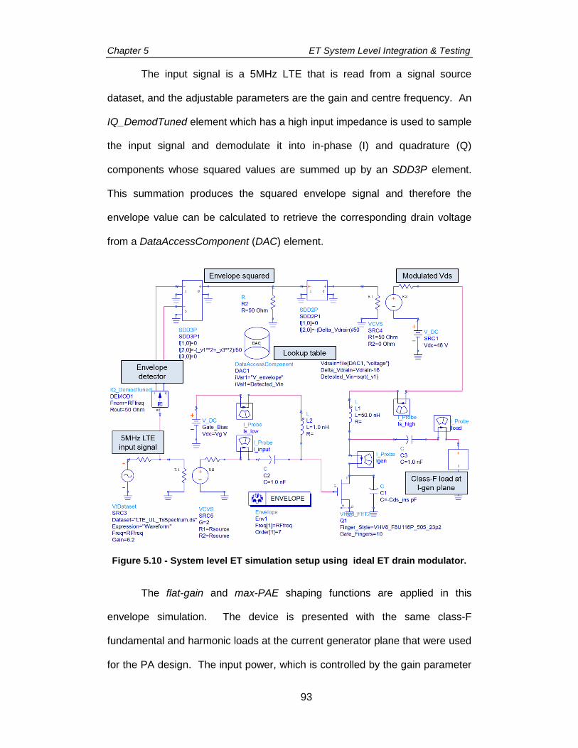
Chapter 5 ET System Level Integration & Testing
93
The input signal is a 5MHz LTE that is read from a signal source
dataset, and the adjustable parameters are the gain and centre frequency. An
IQ_DemodTuned element which has a high input impedance is used to sample
the input signal and demodulate it into in-phase (I) and quadrature (Q)
components whose squared values are summed up by an SDD3P element.
This summation produces the squared envelope signal and therefore the
envelope value can be calculated to retrieve the corresponding drain voltage
from a DataAccessComponent (DAC) element.
Figure 5.10 - System level ET simulation setup using ideal ET drain modulator.
The flat-gain and max-PAE shaping functions are applied in this
envelope simulation. The device is presented with the same class-F
fundamental and harmonic loads at the current generator plane that were used
for the PA design. The input power, which is controlled by the gain parameter
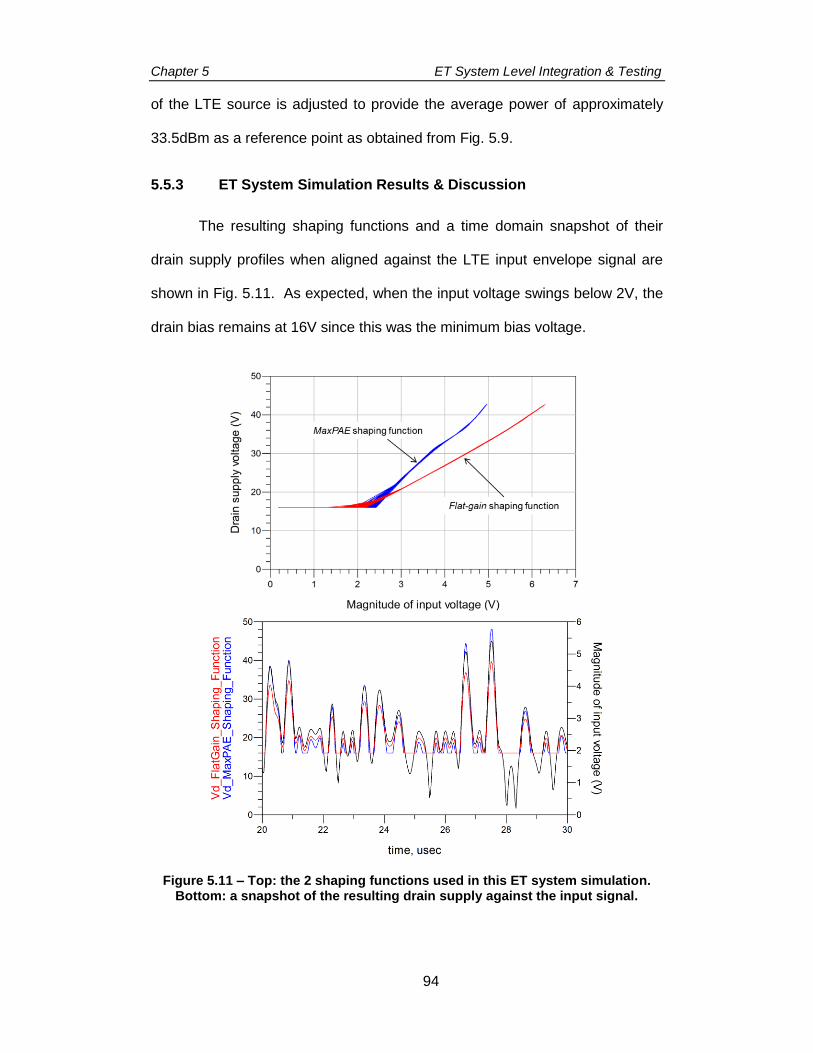
Chapter 5 ET System Level Integration & Testing
94
of the LTE source is adjusted to provide the average power of approximately
33.5dBm as a reference point as obtained from Fig. 5.9.
5.5.3 ET System Simulation Results & Discussion
The resulting shaping functions and a time domain snapshot of their
drain supply profiles when aligned against the LTE input envelope signal are
shown in Fig. 5.11. As expected, when the input voltage swings below 2V, the
drain bias remains at 16V since this was the minimum bias voltage.
Figure 5.11 – Top: the 2 shaping functions used in this ET system simulation. Bottom: a snapshot of the resulting drain supply against the input signal.
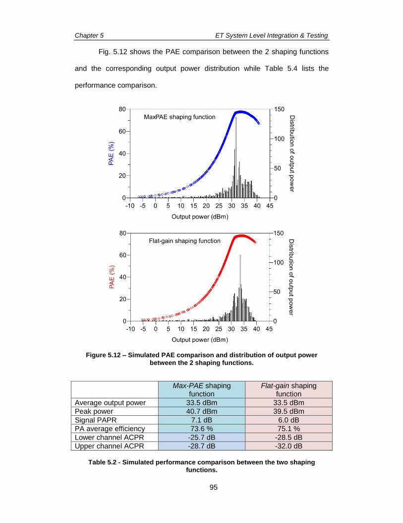
Chapter 5 ET System Level Integration & Testing
95
Fig. 5.12 shows the PAE comparison between the 2 shaping functions
and the corresponding output power distribution while Table 5.4 lists the
performance comparison.
Figure 5.12 – Simulated PAE comparison and distribution of output power between the 2 shaping functions.
Max-PAE shaping function
Flat-gain shaping function
Average output power 33.5 dBm 33.5 dBm
Peak power 40.7 dBm 39.5 dBm
Signal PAPR 7.1 dB 6.0 dB
PA average efficiency 73.6 % 75.1 %
Lower channel ACPR -25.7 dB -28.5 dB
Upper channel ACPR -28.7 dB -32.0 dB
Table 5.2 - Simulated performance comparison between the two shaping functions.

Chapter 5 ET System Level Integration & Testing
96
Several observations can be made about the simulation results. Firstly,
the average efficiency was 1.5%-point higher for the flat-gain shaping function
for this 5MHz LTE input signal. This was initially indicated from Fig. 5.9 where
not only the trade-off in PAE was observed to be minimal when the flat-gain
shaping function was in use, but also, below the average power the PAE for
the flat-gain shaping function started to go higher than the max-PAE shaping
function.
Secondly, the output signal PAPR varied with the shaping function used
because of the gain variation at different drain voltages. The max-PAE
shaping function has a relatively higher overall gain than the flat-gain shaping
function. In this simulation in order to get the same average power of
33.5dBm, the signal PAPR was 7.1dB and 6.0dB for the max-PAE and flat-
gain shaping functions, respectively. If the PAPR was used as a normalizing
factor the resulting average power would be different.
Thirdly, in this simulation the flat-gain shaping was formulated to obtain
a constant 14.5dB gain as shown in Fig. 5.9, which takes effect from peak
power to 10dB output back-off. Although its resulting ACPR performance was
found to be approximately 3dB better than the max-PAE shaping function, it
was only able to reach -32dBc at best. This number was very close to the
measured ACPR performance with DPD applied in Table 5.1, where the DPD
takes on the role of flattening the gain profile across the output power range.
Fig. 5.13 shows the simulated spectral plots for the 2 shaping functions.
A closer look into the simulated transconductance plot in Fig. 5.13
shows that the flat-gain shaping function produces a linear relationship

Chapter 5 ET System Level Integration & Testing
97
between the output current and the input voltage, but only for input voltage
range of above 2V magnitude. At lower input level, the soft turn-on
characteristics of the class-B bias started to contribute to the nonlinear
transconductance. This soft turn-on characteristic was also present when
using the maximum PAE shaping function, as it was caused by the gate bias
and not able to be corrected by the ET shaping function. This was also the
case when DPD correction is applied, as only the higher input voltage gets
corrected for linearity leaving residual nonlinearities coming from low input
level. Although the effect of DPD was not simulated here, the flat-gain shaping
function was supposed to perform the same role.
Figure 5.13 – Top: Simulated transconductance curve with ET. Bottom: simulated signal spectrum for the max-PAE (left) and flat-gain (right) shaping
functions.

Chapter 5 ET System Level Integration & Testing
98
5.6 Conclusions
The integration of the class-F PA into a real ET system has been
presented. The measured ET drain efficiency for the PA and ET modulator
combination was 64% with a 5MHz LTE input signal. This number potentially
can be improved with the use of a GaN device which has a smaller knee
region and output capacitance. Even so, this efficiency performance is among
the highest compared to the state-of-the-art ET PA’s in [1-10] which were
mostly GaN-based, as shown in Fig. 5.14.
Figure 5.14 – Comparison with state-of-the-art ET PA’s. The projected result from this work if class-AB was used is also included.
The main challenge in using class-F mode PA in ET is the linearity
performance. The best-case measured ACPR was -32dBc due to the limitation
of the soft turn-on region not being able to be corrected by DPD. As a
comparison, the class-AB mode used in [1] achieved -45dBc while the class-
AB PA in ET from the Opera Net 2 project achieved -40dBc, both with DPD.
Based on the CW measurement and simulation data, the class-AB efficiency
was approximately 8 to 10%-point lower than class-F for this device. With its
70
65
60
55
50
45
40
35
Ave
rag
e d
rain
eff
icie
ncy (
%)
6050403020100
Signal bandwidth (MHz)
[5]
[5,6,10]
[8,9]
[7]
[1]
[2]
[3]
[4]
108642
Frequency (GHz)
[7]
[Projected result with class-AB]
GaN LDMOS (Size indicates power level)
[This work]

Chapter 5 ET System Level Integration & Testing
99
higher gate bias point it is expected to produce comparable ACPR results,
trading-off efficiency. The projected result if class-AB was used in this work is
also shown in Fig. 5.14
Another way to address this is to have a gate bias variation as a
function of the input envelope, which would raise the gate bias above pinch-off
at low input levels, just enough to meet the desired ACPR performance. This
is explored in simulation in Chapter 8 under Future Work, which presents an
opportunity of improving linearity while retaining some level of class-F
efficiency performance. Another way is to use an alternative nonlinear
correction method that would also address the nonlinearities at low input
levels.
Another aspect of the PA performance that was not discussed in this
chapter is bandwidth. The class-F PA has a limited bandwidth from its
narrowband matching network design. The continuous class-F mode, which is
an extension of this class-F mode developed to increase its bandwidth will be
discussed the next chapter, where the behaviour of continuous mode PA’s in a
variable drain setting for an LDMOS device is investigated.
5.7 References
[1] K. Jungjoon, S. Jungwhan, J. Seunghoon, K. Seokhyeon, and K. Bumman, "Optimization of Envelope Tracking Power Amplifier for Base-Station Applications," Microwave Theory and Techniques, IEEE Transactions on, vol. 61, pp. 1620-1627, 2013.
[2] P. Draxler, S. Lanfranco, D. Kimball, C. Hsia, J. Jeong, J. van de Sluis, et al., "High Efficiency Envelope Tracking LDMOS Power Amplifier for W-CDMA," in Microwave Symposium Digest, 2006. IEEE MTT-S International, 2006, pp. 1534-1537.
[3] D. F. Kimball, J. Jeong, H. Chin, P. Draxler, S. Lanfranco, W. Nagy, et al., "High-Efficiency Envelope-Tracking W-CDMA Base-Station

Chapter 5 ET System Level Integration & Testing
100
Amplifier Using GaN HFETs," Microwave Theory and Techniques, IEEE Transactions on, vol. 54, pp. 3848-3856, 2006.
[4] J. H. Kim, G. D. Jo, J. H. Oh, Y. H. Kim, K. C. Lee, J. H. Jung, et al., "High-Efficiency Envelope-Tracking Transmitter With Optimized Class-F-1 Amplifier and 2-bit Envelope Amplifier for 3G LTE Base Station," IEEE Transactions on Microwave Theory and Techniques, vol. 59, pp. 1610-1621, 2011.
[5] J. J. Yan, P. Theilmann, and D. F. Kimball, "A High Efficiency 780 MHz GaN Envelope Tracking Power Amplifier," in 2012 IEEE Compound Semiconductor Integrated Circuit Symposium (CSICS), 2012, pp. 1-4.
[6] H. Tango, T. Hashinaga, K. Totani, H. Kuriyama, Y. Hamada, and T. Asaina, "A 60% efficient envelope tracking power amplifier for 40W, 2.6GHz LTE base station with in/output harmonic tuning," in Microwave Symposium Digest (IMS), 2013 IEEE MTT-S International, 2013, pp. 1-4.
[7] P. T. Theilmann, J. J. Yan, C. Vu, J. S. Moon, H. P. Moyer, and D. F. Kimball, "A 60MHz Bandwidth High Efficiency X-Band Envelope Tracking Power Amplifier," in 2013 IEEE Compound Semiconductor Integrated Circuit Symposium (CSICS), 2013, pp. 1-4.
[8] G. Collins, J. Fisher, F. Radulescu, J. Barner, S. Sheppard, R. Worley, et al., "C-band and X-band class F, F-1 GaN MMIC PA design for envelope tracking systems," in Microwave Conference (EuMC), 2015 European, 2015, pp. 1172-1175.
[9] Y. Liu, C. S. Yoo, J. Fairbanks, J. Yan, D. Kimball, and P. Asbeck, "A 53% PAE envelope tracking GaN power amplifier for 20MHz bandwidth LTE signals at 880MHz," in 2016 IEEE Topical Conference on Power Amplifiers for Wireless and Radio Applications (PAWR), 2016, pp. 30-32.
[10] J. Kim, J. Moon, J. Son, S. Jee, J. Lee, J. Cha, et al., "Highly efficient envelope tracking transmitter by utilizing sinking current," in Microwave Conference (EuMC), 2011 41st European, 2011, pp. 1197-1200.
Chapter 6 Utilising Continuous Mode PA in ET & the Varactor Effect
101
Chapter 6
Utilising Continuous Mode Power
Amplifiers in Envelope Tracking
& the Varactor Effect
6.1 Introduction
High-efficiency mode power amplifiers such as class-F provide a high-
efficiency performance but only over narrow bandwidth because the
optimisation of the output matching network is done at a single frequency. To
mitigate this limitation and maintain a high efficiency performance over wider
bandwidth, a concept of extending the design space for the PA modes was
introduced by Cripps and Tasker in [1]. In that work, a new design space was
presented identifying a continuum between class-B and class-J, enabling a
design that maintains a class-B performance in terms of power and efficiency,
and that as a result paves the way for high-efficiency mode design over
considerable bandwidth. In [2] the continuous mode theory was extended to
class-F, validating a new design space using an active load-pull measurement
setup that led to the realization of a continuous class-F PA in [3] which
produced a class-F level efficiency of 74% over an octave bandwidth using a
10W GaN device, with only a small variation in output power.
For the same periphery, an LDMOS device however has a relatively
large output capacitance compared to GaN [4] and its operation in a

Chapter 6 Utilising Continuous Mode PA in ET & the Varactor Effect
102
continuous class-F mode of operation has not been experimentally
investigated before in literature at the time of writing.
The first objective of this chapter is to fill this gap and investigate how
far the class-F power amplifier performance obtained with an LDMOS device in
Chapter 4 can be maintained over bandwidth, which is represented by the
continuous class-F mode of operation.
The second objective is to explore the application of a continuous mode
PA in an envelope tracking (ET) setting. A theoretical analysis of integrating a
continuous class-F amplifier in ET was first presented in [5], but in this case the
analysis was limited to simulation and did not include an experimental
validation. This chapter aims to extend that analysis for both simulation and
load-pull measurements, in a variable drain bias environment which represents
an ET application.
The third objective of this chapter is to identify and analyse in detail the
limitations presented by the nonlinear output capacitance CDS to the continuous
mode of operation.
This chapter begins with an overview of the continuous mode theory of
class-BJ and continuous class-F, followed by the experimental investigation of
applying continuous class-F to an LDMOS device in fixed and variable drain
bias settings. The results obtained from simulation and measurements
suggest some difficulty of maintaining a continuous mode of operation due to
the variation of the device CDS as a function of output voltage, or the varactor
effect. The final section of this chapter presents a novel mathematical analysis
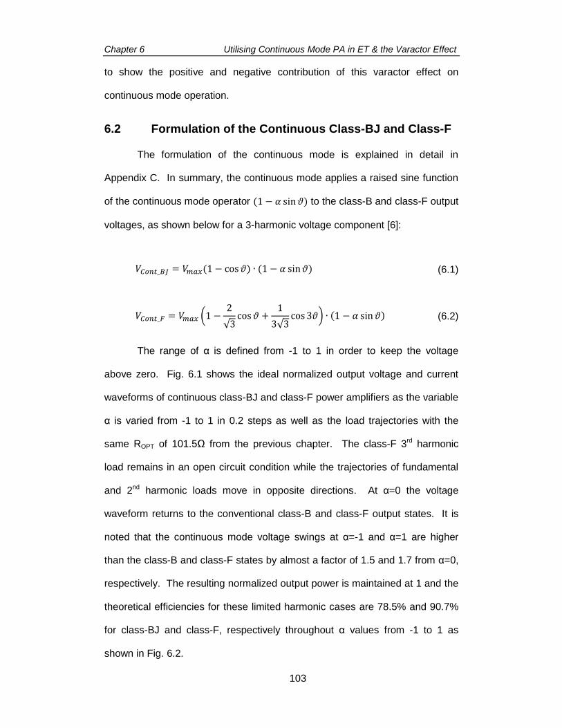
Chapter 6 Utilising Continuous Mode PA in ET & the Varactor Effect
103
to show the positive and negative contribution of this varactor effect on
continuous mode operation.
6.2 Formulation of the Continuous Class-BJ and Class-F
The formulation of the continuous mode is explained in detail in
Appendix C. In summary, the continuous mode applies a raised sine function
of the continuous mode operator (1 − 𝛼 sin 𝜗) to the class-B and class-F output
voltages, as shown below for a 3-harmonic voltage component [6]:
𝑉𝐶𝑜𝑛𝑡_𝐵𝐽 = 𝑉𝑚𝑎𝑥(1 − cos 𝜗) ∙ (1 − 𝛼 sin 𝜗) (6.1)
𝑉𝐶𝑜𝑛𝑡_𝐹 = 𝑉𝑚𝑎𝑥 (1 −2
√3cos 𝜗 +
1
3√3cos 3𝜗) ∙ (1 − 𝛼 sin 𝜗) (6.2)
The range of α is defined from -1 to 1 in order to keep the voltage
above zero. Fig. 6.1 shows the ideal normalized output voltage and current
waveforms of continuous class-BJ and class-F power amplifiers as the variable
α is varied from -1 to 1 in 0.2 steps as well as the load trajectories with the
same ROPT of 101.5Ω from the previous chapter. The class-F 3rd harmonic
load remains in an open circuit condition while the trajectories of fundamental
and 2nd harmonic loads move in opposite directions. At α=0 the voltage
waveform returns to the conventional class-B and class-F output states. It is
noted that the continuous mode voltage swings at α=-1 and α=1 are higher
than the class-B and class-F states by almost a factor of 1.5 and 1.7 from α=0,
respectively. The resulting normalized output power is maintained at 1 and the
theoretical efficiencies for these limited harmonic cases are 78.5% and 90.7%
for class-BJ and class-F, respectively throughout α values from -1 to 1 as
shown in Fig. 6.2.
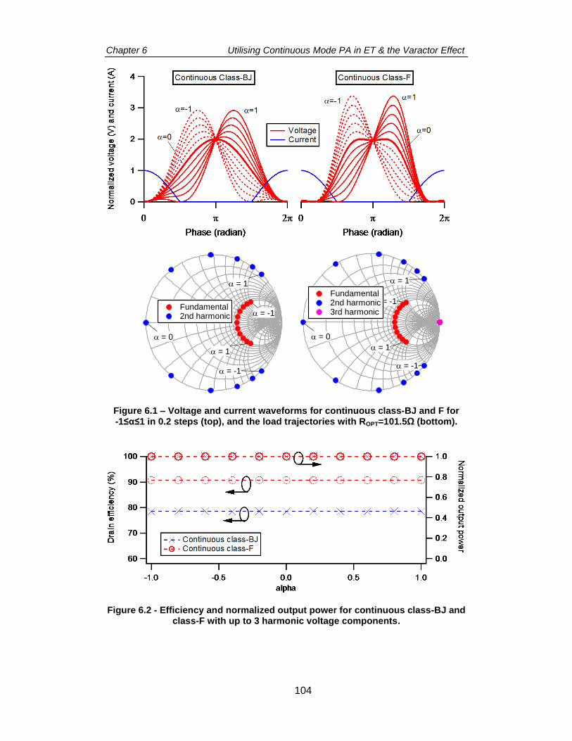
Chapter 6 Utilising Continuous Mode PA in ET & the Varactor Effect
104
Figure 6.1 – Voltage and current waveforms for continuous class-BJ and F for -1≤α≤1 in 0.2 steps (top), and the load trajectories with ROPT=101.5Ω (bottom).
Figure 6.2 - Efficiency and normalized output power for continuous class-BJ and class-F with up to 3 harmonic voltage components.
2.0
1.5
1.0
0.5
0.0
-0.5
-1.0
-1.0 -0.5 0.0 0.5 1.0
= -1
= 1
= 1
= -1
= 0
Fundamental 2nd harmonic
2.0
1.5
1.0
0.5
0.0
-0.5
-1.0
-1.0 -0.5 0.0 0.5 1.0
= -1
= 1
= 1
= -1
= 0
Fundamental 2nd harmonic 3rd harmonic

Chapter 6 Utilising Continuous Mode PA in ET & the Varactor Effect
105
The analysis in Chapter 3 was performed on a class-F mode, which is a
subset of the continuous class-F mode with α=0. The work in this chapter
further extends the investigation to include simulations and measurements at
the full range of α values from -1 to 1 which translates into the full range of the
continuous class-F mode. The continuous class-F mode analysis will be
shown in 2 stages: at a single drain bias in Section 6.3, and in a variable drain
bias setting in Section 6.4.
6.3 Investigating the Continuous Class-F Mode of an
LDMOS Device at a Single Drain Bias
6.3.1 Characterisation Method: Continuous Class-F at 28V Bias
Using the active load-pull system and also Keysight ADS, the 10W
LDMOS device from the previous chapter was initially setup to operate in
class-F mode (α=0) at 28V drain bias with a fundamental load of 101.5Ω and
driven to approximately 1dB into compression. The continuous class-F mode
was then obtained by applying the fundamental and harmonic loads shown in
Fig. 6.1 at the device current generator plane.
As for the input power level, there were 2 scenarios that were analysed;
firstly a constant maximum drain current (IMAX), and then with a constant input
power (PIN) at the gate terminal. For the first scenario, the input drive at each
value of α was adjusted such that the measured peak drain current remained
constant, which was the approach used in [1, 7]. The assumption is that the
half-rectified current output waveform should remain constant as α is varied
within the continuous mode range, therefore any fluctuation in current is due to
the change in input power as a function of frequency, represented by α.

Chapter 6 Utilising Continuous Mode PA in ET & the Varactor Effect
106
For comparison, in the second scenario (constant PIN) the input drive
level was adjusted such that the gate terminal was always presented with a
constant input power after taking account of mismatch loss, as α was varied
from -1 to 1. Hence this scenario does not compensate for the change in the
drain current and provides an insight of the varactor effect of the device
nonlinear CDS on continuous mode PA’s. In a real circuit, this takes away the
effect of frequency response of the input matching network and presents the
gate with the intended constant power throughout the continuous mode range.
This scenario is also relevant when it comes to the implementation of the ET
shaping function, where a given input power is used to determine the required
operating drain bias.
6.3.2 Results & Discussions: Continuous Class-F at 28V Bias
Fig. 6.3 shows the measured voltage and current waveforms of the
continuous class-F mode at 28V drain bias. The reference state α=0 produced
a waveform current maximum of 600mA corresponding to an input power of
11dBm at the gate terminal. Therefore these values are used for the constant-
IMAX and constant-PIN scenarios, respectively.
Several observations are made from the voltage and current waveform
measurements at 28V drain bias. Firstly for the constant IMAX scenario, even
though the current waveform peak reached the desired value of 600mA for
each value of α, the current waveform shape had changed considerably.
Targeting a constant IMAX required a higher drive level on the positive α region
as shown in Fig. 6.4. This is consistent with [7, 8], where the continuous mode
was setup with its drive level adjusted to compensate for changes in the drain
current.
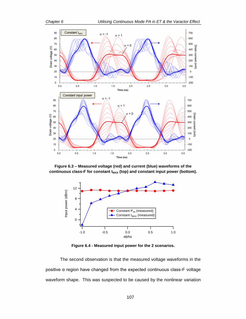
Chapter 6 Utilising Continuous Mode PA in ET & the Varactor Effect
107
Figure 6.3 – Measured voltage (red) and current (blue) waveforms of the
continuous class-F for constant IMAX (top) and constant input power (bottom).
Figure 6.4 - Measured input power for the 2 scenarios.
The second observation is that the measured voltage waveforms in the
positive α region have changed from the expected continuous class-F voltage
waveform shape. This was suspected to be caused by the nonlinear variation
12
8
4
0
Inp
ut
po
wer
(dB
m)
-1.0 -0.5 0.0 0.5 1.0
alpha
Constant PIN (measured)
Constant IMAX (measured)

Chapter 6 Utilising Continuous Mode PA in ET & the Varactor Effect
108
of the device CDS, or the varactor effect, where the displacement current
changes the optimum fundamental and harmonic load locations from the
theoretical trajectory shown in Fig 6.1. This phenomenon is further explored in
Section 6.5.
If the input power at the gate was kept constant (scenario 2), the
voltage waveforms that are closer to the expected shape were observed but
the voltage swings at negative α values were bigger than those of positive α
values. The peak drain current also increased at the negative α values
compared to α=0 and positive α values. The increase and decrease of peak
voltage and current waveforms are another suspected phenomenon attributed
to the nonlinear CDS.
The measured PAE and output power performance for the 2 scenarios
are compared in Fig. 6.5 together with simulation results. In the case of
constant PIN, the efficiency and output power were relatively higher at α<0
values compared to α>0 with a difference of up to 12%-point and 2dB,
respectively. The same trend was also observed in simulation with even a
bigger delta: 25%-point difference in PAE and 3.4dB in output power. This is
suspected to be another artefact of the nonlinear CDS effect which will be
discussed further in Section 6.5.
By comparison the constant IMAX scenario showed a more consistent
output power performance especially for α between -0.8 and 0.8. However its
PAE performance behaviour trend was similar to the constant PIN scenario with
the α<0 region generally exhibiting a higher PAE than those of α>0. For the
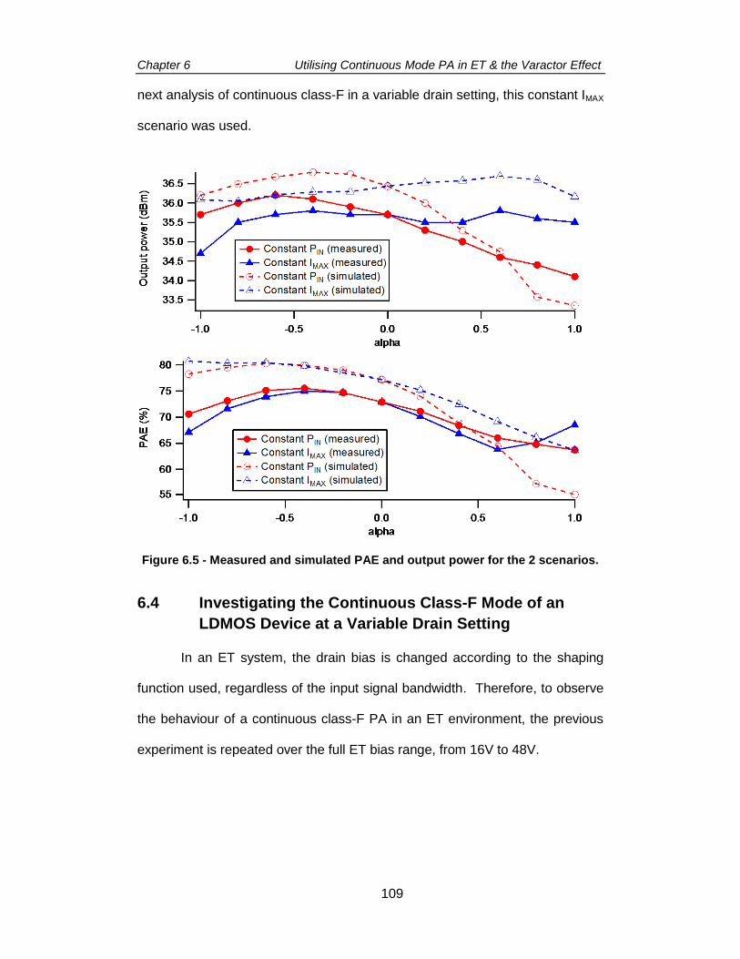
Chapter 6 Utilising Continuous Mode PA in ET & the Varactor Effect
109
next analysis of continuous class-F in a variable drain setting, this constant IMAX
scenario was used.
Figure 6.5 - Measured and simulated PAE and output power for the 2 scenarios.
6.4 Investigating the Continuous Class-F Mode of an
LDMOS Device at a Variable Drain Setting
In an ET system, the drain bias is changed according to the shaping
function used, regardless of the input signal bandwidth. Therefore, to observe
the behaviour of a continuous class-F PA in an ET environment, the previous
experiment is repeated over the full ET bias range, from 16V to 48V.

Chapter 6 Utilising Continuous Mode PA in ET & the Varactor Effect
110
6.4.1 Characterisation Method: Continuous Class-F at ET Bias Range
of 16V–48V
The same flat-gain shaping function from Chapter 3 was applied in this
characterisation process at α=0 to define the relationship between input power
and drain bias. For each bias value, the α value was then varied between -1 to
1 in 0.2 steps while the drive level was adjusted to maintain a constant IMAX.
The constant IMAX normalizing method was selected for consistency reason
with previous works in [1, 7]. Both simulation and load-pull measurements
were performed under these settings at 900MHz. A fixed de-embedding
approach was used for the CDS which corresponds to the 28V drain bias
condition, making the 28V class-F mode the reference setting.
Additionally, the simulation was also performed at a significantly
reduced frequency of 9MHz to remove the effect of CDS (and other parasitics),
and to isolate its impact on device performance. According to the device
model, the value of CDS at 28V bias is 1.3pF, which gives rise to a shunt
reactance of 136Ω at 900MHz and 13.6kΩ at 9MHz. With a 101.5Ω load the
CDS effect is therefore negligible at 9MHz.
6.4.2 Simulation and Measurement Results: Continuous Class-F in a
Variable Drain Setting
The parameter of interest in this analysis is the efficiency performance
as a function of α and drain voltage. Fig. 6.6 shows the PAE contour plot
comparison between measurement and simulation as α was varied from -1 to 1
for each drain bias. The shaded areas in the plots indicate the condition where
the target IMAX (obtained from α=0 reference setting) was not achieved at these
combinations of α and drain bias values. For comparison, the simulation at
9MHz represents a scenario of negligible CDS effect.
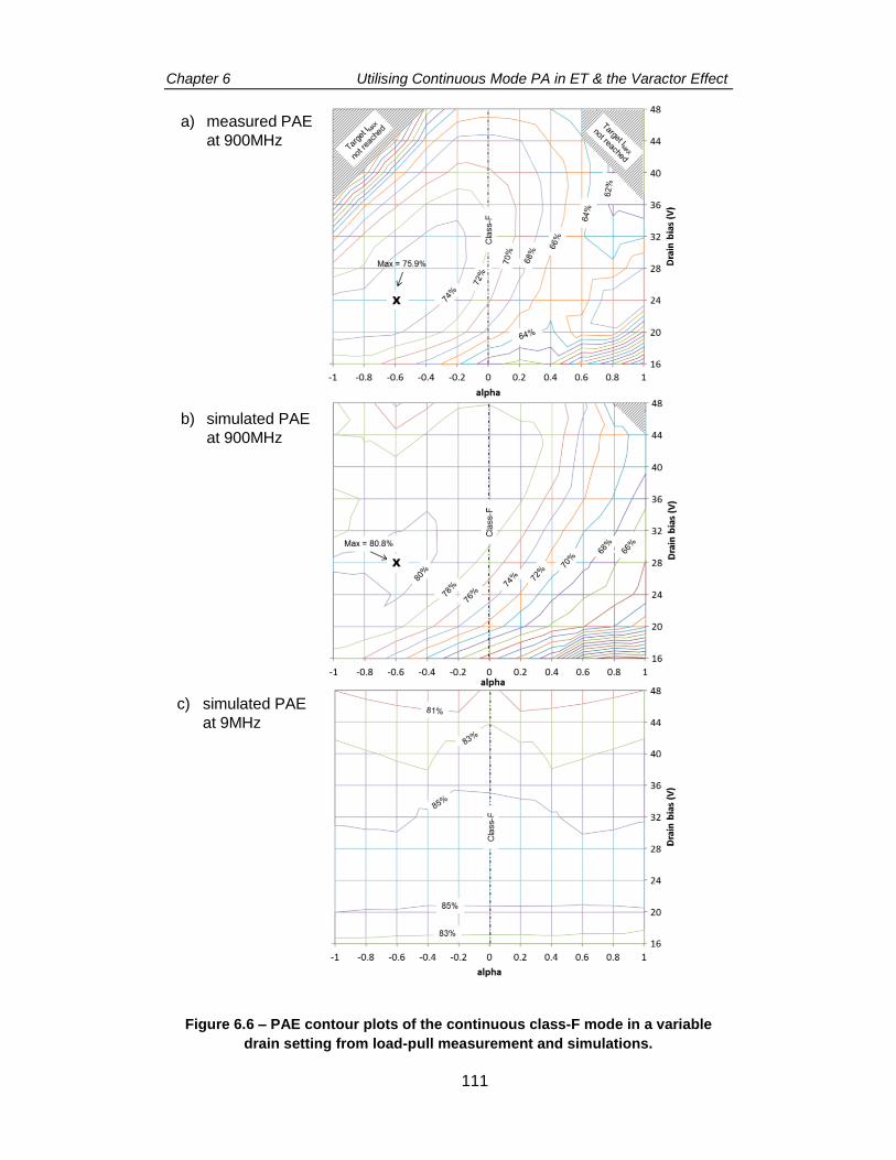
Chapter 6 Utilising Continuous Mode PA in ET & the Varactor Effect
111
Figure 6.6 – PAE contour plots of the continuous class-F mode in a variable
drain setting from load-pull measurement and simulations.
a) measured PAE
at 900MHz
b) simulated PAE
at 900MHz
c) simulated PAE
at 9MHz

Chapter 6 Utilising Continuous Mode PA in ET & the Varactor Effect
112
At 900MHz, an almost diagonal plateau contour was observed from
both measurement and simulation. Relative to the class-F 28V bias reference
setting, the high-PAE region stretched towards the combination of low drain
bias and negative α values as well as high drain bias and positive α values
before degrading at extreme combinations of α and drain bias. The measured
PAE peaked at α=-0.6 and 24V bias where it was approximately 5%-point
higher than the class-F PAE. A similar trend was observed from simulation at
900MHz where the PAE peaked at α=-0.6 and 28V drain bias.
The simulation at 9MHz produced the expected almost-ideal outcome
where only the drain bias variation affects the PAE performance while
exhibiting a much less dependency on α. The slight PAE degradation with
drain bias was a result of different optimum load requirements at different bias
points whilst the device was terminated with a fixed 101.5Ω load.
6.4.3 Discussions
From the measured and simulated results of applying continuous class-
F mode in a variable drain setting it was observed that there exists a region
around α=-0.6 where the PAE performance was enhanced relative to the class-
F (α=0) setting. This localized high-PAE region was not observed when the
CDS effect is removed.
Importantly, for the 900MHz case where the CDS is active, the PAE was
observed to degrade for positive α, and improve significantly in the negative α
region, relative to the class-F (α=0) state. This phenomenon was caused by
the nonlinear CDS property of the device and is mathematically analysed in the
next section and experimentally validated in Chapter 7.
Chapter 6 Utilising Continuous Mode PA in ET & the Varactor Effect
113
The measured PAE at 28V bias in the variable drain experiment in
Section 6.4 had different performance characteristics compared to the single
bias experiment in Section 6.3 due to a different selection of compression level
at the α=0 reference setting. The single bias point experiment was conducted
at 1dB gain compression at VDS=28V whereas the variable drain bias
experiment used a pre-defined shaping function which resulted in a 2dB
compression level at 28V bias. It is therefore noted that the higher
compression level causes a greater PAE enhancement at α=-0.6. One of the
possible explanations is that at the higher compression level, the steep part of
the CDS curve in the knee region is invoked, producing a higher displacement
current magnitude.
The uncertain contribution of the displacement current at other α values
poses an issue of using a constant IMAX as the normalizing method in a
continuous mode PA characterisation. The other issue is that there are
regions where the target IMAX is not achieved due to the superposition of
displacement current from the nonlinear CDS which changes overall current
waveform shape.
From the results, it was observed that the varactor effect on continuous
class-F both improves and degrades the PAE. In addition, the required
fundamental and harmonic load locations are modified, and the expected
continuous class-F current (and as a consequence voltage) waveforms altered
due to the contribution of displacement current, presenting a challenge in the
characterisation process of a continuous mode PA from waveform engineering
perspective. The next section presents a novel mathematical analysis of the

Chapter 6 Utilising Continuous Mode PA in ET & the Varactor Effect
114
effect of the CDS variation, or the varactor effect, on continuous mode PA’s,
focusing on continuous class-BJ which is the most basic continuous mode.
6.5 A Novel Mathematical Analysis of the Varactor Effect
on Continuous Mode Power Amplifiers
The ideal formulation of continuous class-BJ and class-F impedance
trajectories shown in the previous section assumes a fixed CDS. In a real
device however, the value of CDS changes nonlinearly with drain voltage, in a
way that is specific to the device technology used. Taking account of the
nonlinear CDS to VDS relationship changes the impedance formulation for
continuous modes, even at a single bias point. This is not only because of the
CDS variation during a drain voltage swing, but also the modification of the
output voltage and hence the output capacitance, by the continuous mode
operator α as it is varied from -1 to 1. The variation in CDS changes the nature
of the current delivered to the load, which then changes the effective load seen
by the current generator plane.
This section aims to provide a mathematical explanation of the varactor
effect on continuous mode power amplifiers, focusing on class-BJ power
amplifier as it is the simplest form of continuous mode and involves only
fundamental and 2nd harmonic load analysis. The objective is to understand
how the varactor and its displacement current change the fundamental and 2nd
harmonic impedances seen by the current generator plane, when the output
voltage adheres to the continuous class-BJ voltage definition. The ultimate
objective is to understand its impact on the device output power and drain
efficiency.
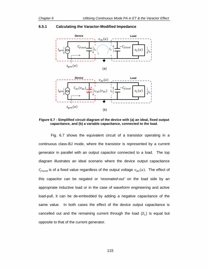
Chapter 6 Utilising Continuous Mode PA in ET & the Varactor Effect
115
6.5.1 Calculating the Varactor-Modified Impedance
Figure 6.7 - Simplified circuit diagram of the device with (a) an ideal, fixed output capacitance, and (b) a variable capacitance, connected to the load.
Fig. 6.7 shows the equivalent circuit of a transistor operating in a
continuous class-BJ mode, where the transistor is represented by a current
generator in parallel with an output capacitor connected to a load. The top
diagram illustrates an ideal scenario where the device output capacitance
𝐶𝑓𝑖𝑥𝑒𝑑 is of a fixed value regardless of the output voltage 𝑣𝑑𝑠(𝛼). The effect of
this capacitor can be negated or ‘resonated-out’ on the load side by an
appropriate inductive load or in the case of waveform engineering and active
load-pull, it can be de-embedded by adding a negative capacitance of the
same value. In both cases the effect of the device output capacitance is
cancelled out and the remaining current through the load (𝑍𝐿) is equal but
opposite to that of the current generator.
Chapter 6 Utilising Continuous Mode PA in ET & the Varactor Effect
116
With the output voltage strictly adhering to the continuous class-BJ
definition, the output impedance seen by the current generator plane is given
by (6.3) and the conventional continuous class-BJ fundamental and 2nd
harmonic load trajectory from Fig. 6.1 is obtained:
𝑍𝑔𝑒𝑛(𝛼) = −𝑣𝑑𝑠(𝛼)
𝑖𝑔𝑒𝑛 (6.3)
where 𝑣𝑑𝑠(𝛼) is the continuous class-BJ voltage as defined in (6.2).
In Fig. 6.7 (b) the ideal capacitor is now replaced with a variable
capacitor, or varactor, whose value depends on the voltage across it. The
static, de-embedding negative capacitor now does not completely cancel out
the varactor current but rather it leaves a residual displacement current which
is dependent on α. The current through the load is now given by:
𝑖𝐿(𝛼) = −[𝑖𝑔𝑒𝑛 + 𝑖𝐶𝑑𝑠(𝛼) − 𝑖𝐶]
= −𝑖𝑔𝑒𝑛 +𝑑𝑣𝑑𝑠(𝛼)
𝑑𝑡[𝐶𝑑𝑠(𝑣𝑑𝑠) − 𝐶𝑓𝑖𝑥𝑒𝑑] (6.5)
With the output voltage constricted to the continuous class-BJ
definition, the addition of this net variable current caused by the varactor
modifies the fundamental and 2nd harmonic load impedances seen from the
current generator plane. It is therefore important to know the C-V
characteristic of the varactor in order to perform this mathematical analysis.
The varactor’s typical behaviour, which is dependent on the output voltage,
can be modelled by the equation:
𝐶𝑑𝑠(𝑣𝑑𝑠) = 𝐶𝑜𝑓𝑓𝑠𝑒𝑡 +𝐶0
(1 +𝑣𝑑𝑠
𝑣0⁄ )
𝑚 (6.6)

Chapter 6 Utilising Continuous Mode PA in ET & the Varactor Effect
117
where 𝐶𝑜𝑓𝑓𝑠𝑒𝑡, 𝐶0, 𝑣0, and 𝑚 are the adjustable parameters that describe the
shape of the C-V curve. In Section 6.5.2 an approximation of the C-V
characteristics is shown using the parameters in (6.6) to match the
manufacturer’s C-V model. Applying (6.6) into (6.5) the load current can now
be expanded to:
𝑖𝐿(𝛼) = −𝑖𝑔𝑒𝑛 +𝑑𝑣𝑑𝑠(𝛼)
𝑑𝑡[𝐶𝑜𝑓𝑓𝑠𝑒𝑡 +
𝐶0
(1 +𝑣𝑑𝑠
𝑣0⁄ )
𝑚 − 𝐶𝑓𝑖𝑥𝑒𝑑] (6.7)
Using FFT operation on the continuous class-BJ voltage described in
(6.1) and the current in (6.7), the resulting fundamental and 2nd harmonic
impedances seen by the current generator can be calculated.
6.5.2 Performing Numerical Analysis with Approximated Device
Parameters
To proceed with this analysis a numerical approximation approach is
used as it simplifies the calculation and also provides a basis for comparison
with the simulation and measurement results. The parameter values are
approximated and based on the device properties and the class-BJ operating
conditions (bias, output voltage and current swings). The FFT operations,
calculations of the impedance, power, and drain efficiency are performed using
Wavemetrics Igor-Pro software.
Maximum voltage magnitude (VMAX) 50V
Maximum current magnitude (IMAX) 0.8A (resulting in 10W output power)
Knee voltage 0V
Conduction angle 180° (Class-B bias)
Frequency 1 GHz
Table 6.1 - Device settings and operating conditions used in the analysis.
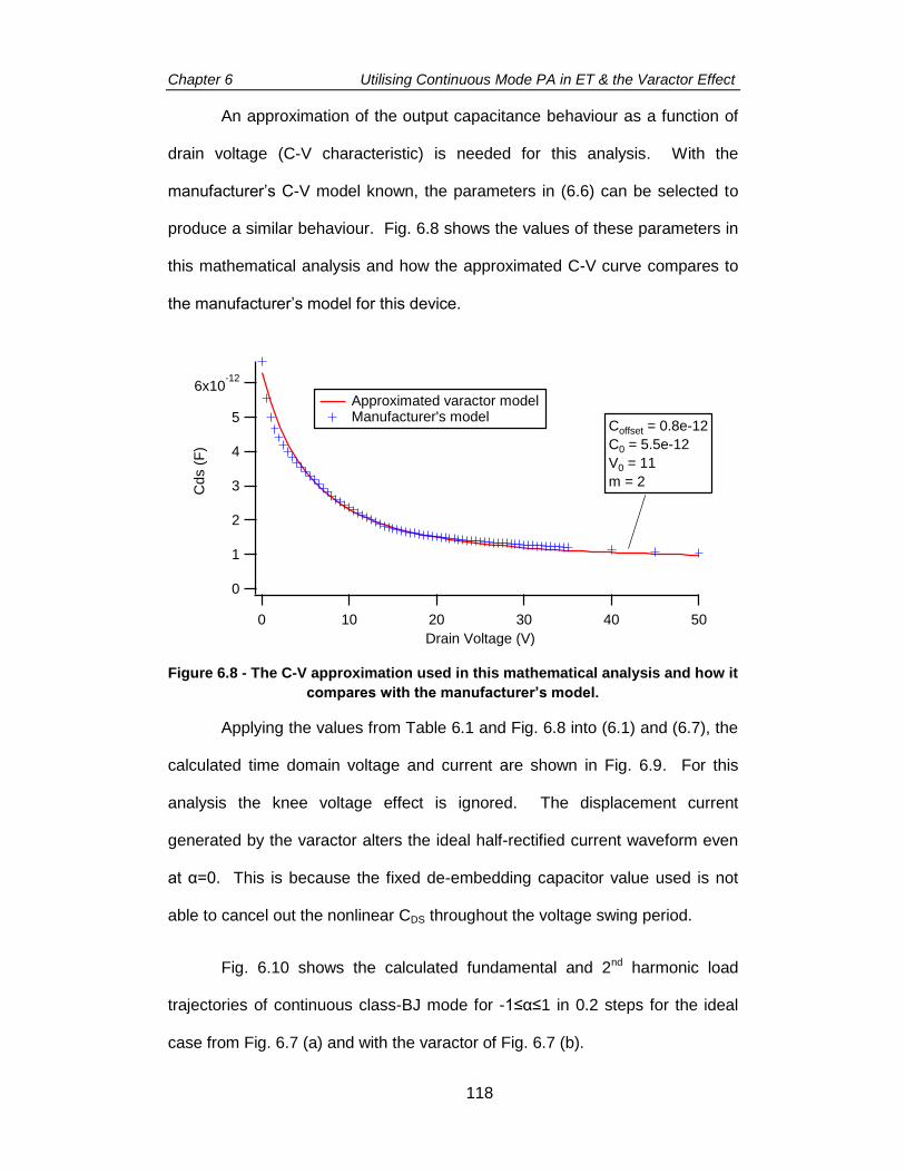
Chapter 6 Utilising Continuous Mode PA in ET & the Varactor Effect
118
An approximation of the output capacitance behaviour as a function of
drain voltage (C-V characteristic) is needed for this analysis. With the
manufacturer’s C-V model known, the parameters in (6.6) can be selected to
produce a similar behaviour. Fig. 6.8 shows the values of these parameters in
this mathematical analysis and how the approximated C-V curve compares to
the manufacturer’s model for this device.
Figure 6.8 - The C-V approximation used in this mathematical analysis and how it
compares with the manufacturer’s model.
Applying the values from Table 6.1 and Fig. 6.8 into (6.1) and (6.7), the
calculated time domain voltage and current are shown in Fig. 6.9. For this
analysis the knee voltage effect is ignored. The displacement current
generated by the varactor alters the ideal half-rectified current waveform even
at α=0. This is because the fixed de-embedding capacitor value used is not
able to cancel out the nonlinear CDS throughout the voltage swing period.
Fig. 6.10 shows the calculated fundamental and 2nd harmonic load
trajectories of continuous class-BJ mode for -1≤α≤1 in 0.2 steps for the ideal
case from Fig. 6.7 (a) and with the varactor of Fig. 6.7 (b).
6x10-12
5
4
3
2
1
0
Cds (
F)
50403020100
Drain Voltage (V)
Approximated varactor model Manufacturer's model
Coffset = 0.8e-12
C0 = 5.5e-12
V0 = 11
m = 2
Chapter 6 Utilising Continuous Mode PA in ET & the Varactor Effect
119
Figure 6.9 – Calculated time domain voltage (red) and current (blue) waveforms.
Figure 6.10 – Calculated class-BJ fundamental and 2nd harmonic loads as a function of α for a fixed CDS (left) and a variable CDS (right).
6.5.3 Observations and Discussions from the Mathematical Analysis
Fig. 6.10 indicates that with the varactor effect in place, the
fundamental and 2nd harmonic load trajectories have been modified in order to
maintain the established class-BJ output voltage waveforms with the varactor
in effect. The calculated 2nd harmonic load trajectory goes inside the Smith
2.0
1.5
1.0
0.5
0.0
-0.5
-1.0
-1.0 -0.5 0.0 0.5 1.0
= -1
= 1
= 1
= -1
= 0
Fundamental 2nd harmonic
2.0
1.5
1.0
0.5
0.0
-0.5
-1.0
-1.0 -0.5 0.0 0.5 1.0
= -1
= 1
= 1
= -1
= 0
Fundamental 2nd harmonic
= 0

Chapter 6 Utilising Continuous Mode PA in ET & the Varactor Effect
120
chart for -1<α<0 indicating the presence of a resistive load requirement and
consequential power dissipation, while for 0<α<1 the 2nd harmonic load
appears outside the Smith chart indicating a varactor related 2nd harmonic
‘injection’ is taking place. It is worth noting that 2nd harmonic injection is an
established way to improve PA efficiency [9-12].
Only at α=0 is the original class-BJ 2nd harmonic load condition
maintained, while at the extreme α values of -1 and 1, the 2nd harmonic load is
located on the edge of the Smith chart, although with a phase offset from the
ideal case. The trajectory of the fundamental load has also been slightly
modified compared to its ideal class-BJ counterpart.
The modification of the load trajectories tallies with the calculated
output power trend as a function of α, for fundamental and 2nd harmonic as
shown in Fig. 6.11. For -1<α<0 as the 2nd harmonic load enters the Smith
chart, the 2nd harmonic output power increases while the fundamental power
drops by the same amount. This is an indication of an energy up-conversion
where the energy at the fundamental frequency is transferred to the 2nd
harmonic frequency. Subsequently the calculated drain efficiency, which
depends on the fundamental power also drops compared to the ideal class-BJ
efficiency for this range of α, as shown in Fig. 6.11.
Conversely and importantly, for 0<α<1, where the 2nd harmonic load
sits outside the Smith chart, energy down-conversion is observed where the
2nd harmonic energy is transferred to the fundamental frequency, causing the
increase in fundamental power by the same amount as the drop in 2nd
harmonic power. For this α range, an interesting observation is that the drain
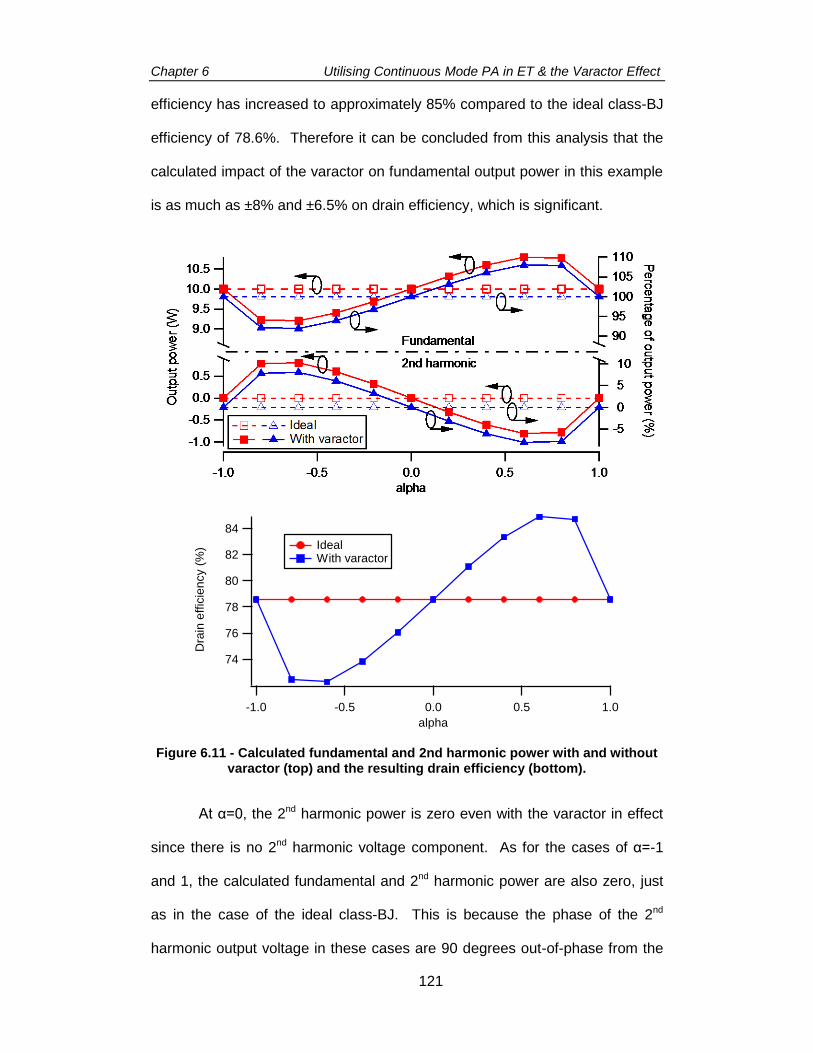
Chapter 6 Utilising Continuous Mode PA in ET & the Varactor Effect
121
efficiency has increased to approximately 85% compared to the ideal class-BJ
efficiency of 78.6%. Therefore it can be concluded from this analysis that the
calculated impact of the varactor on fundamental output power in this example
is as much as ±8% and ±6.5% on drain efficiency, which is significant.
Figure 6.11 - Calculated fundamental and 2nd harmonic power with and without varactor (top) and the resulting drain efficiency (bottom).
At α=0, the 2nd harmonic power is zero even with the varactor in effect
since there is no 2nd harmonic voltage component. As for the cases of α=-1
and 1, the calculated fundamental and 2nd harmonic power are also zero, just
as in the case of the ideal class-BJ. This is because the phase of the 2nd
harmonic output voltage in these cases are 90 degrees out-of-phase from the
84
82
80
78
76
74
Dra
in e
ffic
ien
cy (
%)
-1.0 -0.5 0.0 0.5 1.0
alpha
Ideal With varactor

Chapter 6 Utilising Continuous Mode PA in ET & the Varactor Effect
122
2nd harmonic current. Since the power is the product of the voltage and current
vectors, a 90-degree phase difference produces no 2nd harmonic power and
the power at fundamental is preserved.
6.5.4 Bringing the 2nd Harmonic Load to the Edge of Smith Chart
The varactor causes the 2nd harmonic load to shift inside and then
outside the Smith chart for negative and positive α values, respectively in order
to maintain the continuous class-BJ voltage at the output. For the next step in
this mathematical analysis, it is desirable to relocate these 2nd harmonic loads
to the edge of the Smith chart and there are 2 motivations for doing this.
Firstly, by pulling the 2nd harmonic loads from outside the Smith chart
(in the case of positive α range values) towards the edge, it becomes possible
to achieve through passive network design. Secondly, by pushing the 2nd
harmonic loads from inside the Smith chart towards the edge (in the case of
negative α range values), a high-reflect is presented to the 2nd harmonic
frequency, preventing an energy up-conversion from the fundamental
frequency hence improving efficiency.
The method used to bring the second harmonic loads towards the edge
of the Smith chart is by applying a phase shift to the continuous class-BJ
output voltage. The equation (6.8) below describes the output voltage with the
inclusion of a phase term, Φ.
𝑣𝑑𝑠(𝛼) = 𝑉𝑚𝑎𝑥(1 − 𝑐𝑜𝑠(𝜃 + 𝜑))(1 − 𝛼 𝑠𝑖𝑛(𝜃 + 𝜑)) (6.8)
It is important to note that at α=1 and α=-1, no phase shift is needed
since the 2nd harmonic load for these cases are already located on the edge of
the Smith chart. As for α=0, it will be shown in the next section that a phase
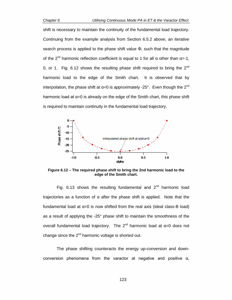
Chapter 6 Utilising Continuous Mode PA in ET & the Varactor Effect
123
shift is necessary to maintain the continuity of the fundamental load trajectory.
Continuing from the example analysis from Section 6.5.2 above, an iterative
search process is applied to the phase shift value Φ, such that the magnitude
of the 2nd harmonic reflection coefficient is equal to 1 for all α other than α=-1,
0, or 1. Fig. 6.12 shows the resulting phase shift required to bring the 2nd
harmonic load to the edge of the Smith chart. It is observed that by
interpolation, the phase shift at α=0 is approximately -25°. Even though the 2nd
harmonic load at α=0 is already on the edge of the Smith chart, this phase shift
is required to maintain continuity in the fundamental load trajectory.
Figure 6.12 – The required phase shift to bring the 2nd harmonic load to the edge of the Smith chart.
Fig. 6.13 shows the resulting fundamental and 2nd harmonic load
trajectories as a function of α after the phase shift is applied. Note that the
fundamental load at α=0 is now shifted from the real axis (ideal class-B load)
as a result of applying the -25° phase shift to maintain the smoothness of the
overall fundamental load trajectory. The 2nd harmonic load at α=0 does not
change since the 2nd harmonic voltage is shorted out.
The phase shifting counteracts the energy up-conversion and down-
conversion phenomena from the varactor at negative and positive α,
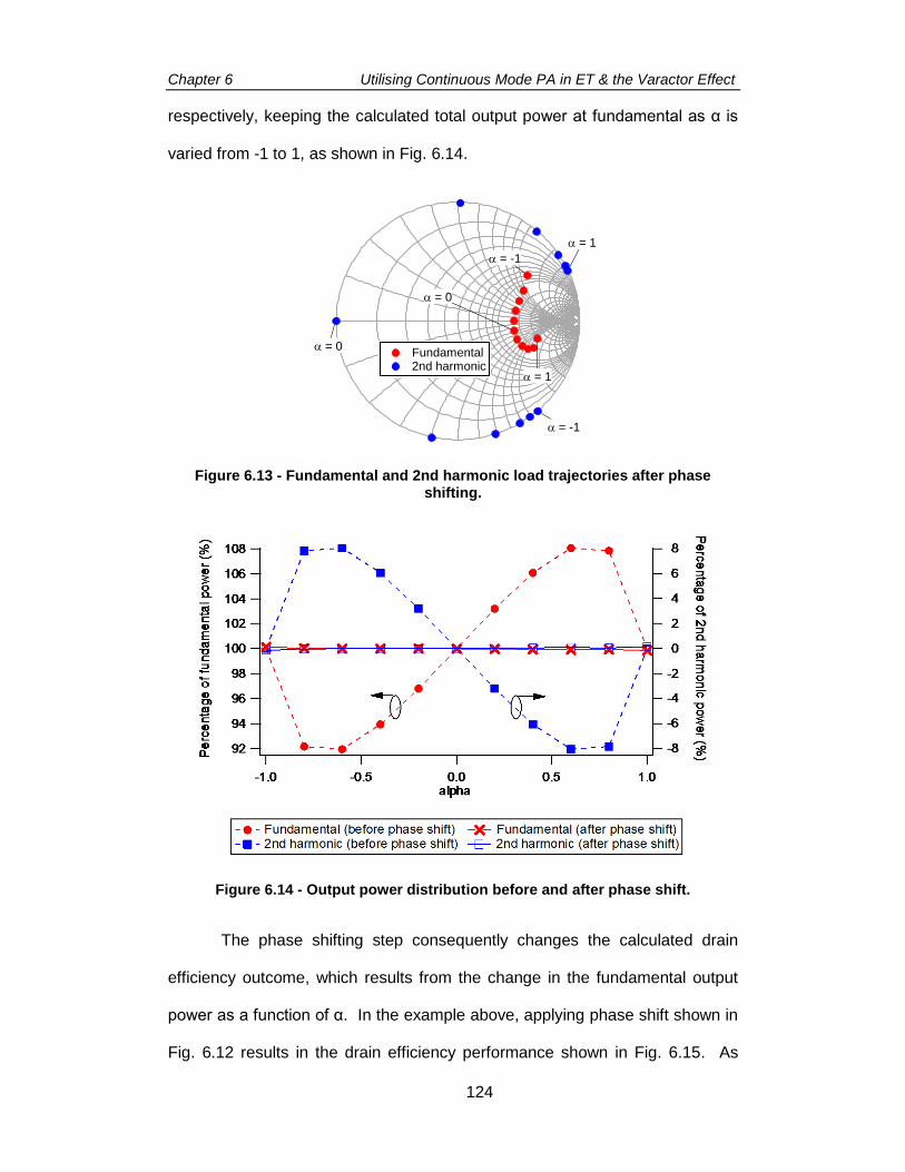
Chapter 6 Utilising Continuous Mode PA in ET & the Varactor Effect
124
respectively, keeping the calculated total output power at fundamental as α is
varied from -1 to 1, as shown in Fig. 6.14.
Figure 6.13 - Fundamental and 2nd harmonic load trajectories after phase shifting.
Figure 6.14 - Output power distribution before and after phase shift.
The phase shifting step consequently changes the calculated drain
efficiency outcome, which results from the change in the fundamental output
power as a function of α. In the example above, applying phase shift shown in
Fig. 6.12 results in the drain efficiency performance shown in Fig. 6.15. As
-1.0
-0.5
0.0
0.5
1.0
-1.0 -0.5 0.0 0.5 1.0
= -1
= 1
= 1
= -1
= 0 Fundamental 2nd harmonic
= 0

Chapter 6 Utilising Continuous Mode PA in ET & the Varactor Effect
125
expected at positive α values, the calculated efficiency drops since the 2nd
harmonic injection effect from the varactor has been removed with the loads
now relocated to the edge of the Smith chart. At α=0, the efficiency drops from
the ideal class-B number of 78.6% to 71% for this example, as the
fundamental load has been shifted from the optimum location on the real axis
of the Smith chart to cater for the overall load trajectory smoothness.
Figure 6.15 - Drain efficiency before and after phase shift.
However for α ≤ -0.4, the calculated drain efficiency is higher than the
theoretical class-B efficiency number, since the varactor effect is now exploited
to provide a 2nd harmonic injection effect within this range of α. The highest
drain efficiency achieved in this example is 85% when α=-0.8. This presents
an interesting proposition in the design of a class-BJ power amplifier, where
the fundamental and 2nd harmonic now are all within the border of the Smith
chart and a higher efficiency performance is possible to be achieved by
exploiting the 2nd harmonic generating properties of the varactor.
85
80
75
70
65
Dra
in e
ffic
iency (
%)
-1.0 -0.5 0.0 0.5 1.0
alpha
Ideal With varactor With varactor + phase shift

Chapter 6 Utilising Continuous Mode PA in ET & the Varactor Effect
126
6.5.5 Comparison with Previous 2nd Harmonic Injection Works
It is useful to revisit previous works where 2nd harmonic injection has
been used for the same purpose and review their results as well as their
methods of implementation.
The proof-of-concept of efficiency enhancement using 2nd harmonic
injection is presented in [9] where an additional source is directly connected at
the input to inject a 2nd harmonic signal. By adjusting the externally injected 2nd
harmonic power, the PAE can be improved by 15% for a 4W GaN HEMT
operating in a class-B mode at 2GHz. In [10] a source pull approach is used to
inject the 2nd harmonic to shape the input waveform, enhancing the PAE of a
pHEMT operating in class-B by 5.9% at 9GHz. In [11] the 2nd harmonic
injection is obtained through a feedback loop with an added auxiliary class-E
mode amplifier, enhancing the main amplifier PAE by 16%-point. An auxiliary
PA is also used in [12] to inject a 2nd harmonic into a main PA operating in
inverse class-F mode at 1GHz. For this particular example the improvement
was not in terms of a higher PAE but in terms of the extended bandwidth of the
high-efficiency (>80%) region, going from 60MHz to 180MHz.
However in these previous works an external circuit is required to
supply the 2nd harmonic signal. The mathematical analysis in this chapter
suggests that the varactor itself can be exploited to generate the 2nd harmonic
injection to improve PA efficiency. In the next chapter the experimental
investigation is performed to explore this possibility.
Chapter 6 Utilising Continuous Mode PA in ET & the Varactor Effect
127
6.6 Conclusions
The first part of this chapter presents the novel experimental work of
integrating continuous class-F mode in an envelope tracking environment
using waveform engineering approach. The observations made from the
measurement results suggested that the varactor positively and negatively
affects the drain efficiency performance of a continuous mode PA even at a
single drain bias. This observation led to a deeper investigation of the varactor
effect on continuous mode PA’s to explain the measurement results.
The second part of this chapter presented the theory of the varactor
effect on continuous mode PA’s, focusing on the most basic continuous mode
which is class-BJ. It can be shown mathematically that the varactor improves
the drain efficiency performance on half of the continuous mode design space
while it degrades the other half, relative to the class-B reference mode. The
mechanism behind the efficiency performance change is the energy
conversion between fundamental and 2nd harmonic. In the case where
efficiency is enhanced, the varactor acts as a 2nd harmonic injection source,
similar to the concept discussed in [9-12]. It is worth noting that the efficiency
improvement amount will also depend on the CDS-VDS characteristics.
The next chapter presents an experimental work to validate the theory
of efficiency enhancement through the varactor alone, and discusses its
limitations.
6.7 References
[1] S. C. Cripps, P. J. Tasker, A. L. Clarke, J. Lees, and J. Benedikt, "On the Continuity of High Efficiency Modes in Linear RF Power Amplifiers," Microwave and Wireless Components Letters, IEEE, vol. 19, pp. 665-667, 2009.
Chapter 6 Utilising Continuous Mode PA in ET & the Varactor Effect
128
[2] V. Carrubba, A. L. Clarke, M. Akmal, J. Lees, J. Benedikt, P. J. Tasker, et al., "The Continuous Class-F Mode Power Amplifier," in Microwave Conference (EuMC), 2010 European, 2010, pp. 1674-1677.
[3] V. Carrubba, J. Lees, J. Benedikt, P. J. Tasker, and S. C. Cripps, "A novel highly efficient broadband continuous class-F RFPA delivering 74% average efficiency for an octave bandwidth," in Microwave Symposium Digest (MTT), 2011 IEEE MTT-S International, 2011, pp. 1-4.
[4] E. McCune, Dynamic Power Supply Transmitters: Cambridge University Press, 2015.
[5] B. Merrick and T. J. Brazil, "Analysis of the integration of envelope tracking with Continuous Class F amplifiers," in Integrated Nonlinear Microwave and Millimetre-Wave Circuits (INMMIC), 2012 Workshop on, 2012, pp. 1-3.
[6] P. Colantonio, F. Giannini, G. Leuzzi, and E. Limiti, "On the class-F power amplifier design," International Journal of Rf and Microwave Computer-Aided Engineering, vol. 9, pp. 129-149, Mar 1999.
[7] V. Carrubba, "Novel highly efficient broadband continuous power amplifier modes," PhD Thesis, Cardiff University, 2012.
[8] V. Carrubba, A. L. Clarke, M. Akmal, Z. Yusoff, J. Lees, J. Benedikt, et al., "Exploring the design space for broadband PA's using the novel continuous inverse class-F mode," in Microwave Conference (EuMC), 2011 41st European, 2011, pp. 333-336.
[9] H. Matsubara, F. Kawanabe, and T. Nojima, "A 2-GHz band experiment on efficiency enhancement of a GaN power amplifier using 2nd harmonic injection," in Microwave Conference, 2008. APMC 2008. Asia-Pacific, 2008, pp. 1-4.
[10] M. Haynes, S. C. Cripps, J. Benedikt, and P. J. Tasker, "PAE improvement using 2nd harmonic source injection at X-band," in Integrated Nonlinear Microwave and Millimetre-Wave Circuits (INMMIC), 2012 Workshop on, 2012, pp. 1-3.
[11] H. R. Bae, C. S. Cho, and J. W. Lee, "Efficiency enhanced class-E power amplifier using the second harmonic injection at the feedback loop," in Microwave Conference (EuMC), 2010 European, 2010, pp. 1042-1045.
[12] M. Seo, H. Lee, J. Gu, H. Kim, J. Ham, W. Choi, et al., "High-Efficiency Power Amplifier Using an Active Second-Harmonic Injection Technique Under Optimized Third-Harmonic Termination," IEEE Transactions on Circuits and Systems II: Express Briefs, vol. 61, pp. 549-553, 2014.

Chapter 7 Exposing the Varactor in Measurement – The Voltage-Pull Method
129
Chapter 7
Exposing the Varactor Effect in
Measurement – The Voltage-Pull
Method
7.1 Introduction
In the previous chapter, the varactor effect on continuous mode PA
performance has been mathematically analysed. The concept of exploiting the
varactor for efficiency improvement has also been proposed using a phase
shifting technique that is theoretically applied to the output voltage.
This chapter presents an experimental investigation of the varactor
effect to validate the theory proposed in Chapter 6 and to investigate the
feasibility of exploiting the varactor for PA efficiency improvement. A novel
measurement method to expose the varactor effect on continuous mode PA’s,
termed the voltage-pull is presented. This method is a modification of the
traditional active load-pull approach with the difference that it uses the output
voltage waveform as the target criteria rather than specific fundamental and
harmonic loads on the Smith chart.
The voltage-pull method was applied both in simulation and in
measurement, to a 50V LDMOS device operating in a continuous class-BJ

Chapter 7 Exposing the Varactor in Measurement – The Voltage-Pull Method
130
mode. The resulting impedance trajectories, output power, and efficiency were
then analysed and compared to the outcomes from the mathematical analysis.
The possibility of exploiting the varactor for efficiency improvement was
then explored using the phase shifting technique on the class-BJ voltage
waveform. The chapter concludes with a discussion on the limitations of
efficiency enhancement using the varactor due to its resistive loss, and
mathematically analyses the lossy-varactor effect in comparison with the
theory presented in Chapter 6.
7.2 Load-Pull Approach vs. Voltage-Pull Approach
The approach to conventional active load-pull uses the concept of a
target load and an algorithm to iteratively change the magnitude and phase of
a synthesized phase coherent signal at the load in order to converge onto the
target. For waveform engineering and specifically continuous mode PA
characterisation, this method relies on de-embedding accuracy to correctly
establish the continuous mode output voltage and current waveforms at the
intrinsic device plane, from the defined loads. However as shown in Chapter
6, a static de-embedding approach will not be able to fully compensate for the
dynamic displacement current generated by the nonlinear CDS.
Characterizing a continuous class-BJ mode for example, by applying a
target load based on the continuous mode formulation from Fig. 6.1 will result
in an output voltage that is different from the expected class-BJ waveforms in
Fig. 6.1 because of the varactor displacement current.
To understand and observe the varactor effect on continuous mode
operation, a different measurement approach is required where the desired
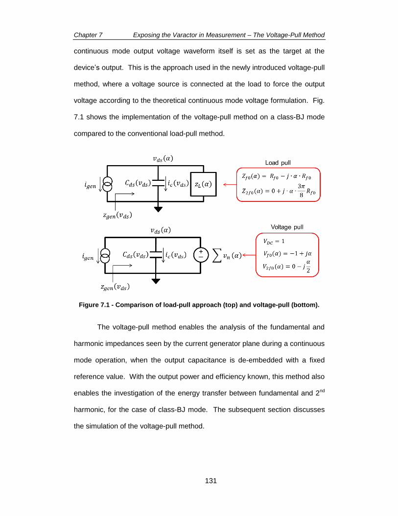
Chapter 7 Exposing the Varactor in Measurement – The Voltage-Pull Method
131
continuous mode output voltage waveform itself is set as the target at the
device’s output. This is the approach used in the newly introduced voltage-pull
method, where a voltage source is connected at the load to force the output
voltage according to the theoretical continuous mode voltage formulation. Fig.
7.1 shows the implementation of the voltage-pull method on a class-BJ mode
compared to the conventional load-pull method.
Figure 7.1 - Comparison of load-pull approach (top) and voltage-pull (bottom).
The voltage-pull method enables the analysis of the fundamental and
harmonic impedances seen by the current generator plane during a continuous
mode operation, when the output capacitance is de-embedded with a fixed
reference value. With the output power and efficiency known, this method also
enables the investigation of the energy transfer between fundamental and 2nd
harmonic, for the case of class-BJ mode. The subsequent section discusses
the simulation of the voltage-pull method.

Chapter 7 Exposing the Varactor in Measurement – The Voltage-Pull Method
132
7.3 Simulation of the Varactor Effect on Continuous
Class-BJ Power Amplifier Using Voltage-Pull
The voltage-pull method can be simulated in Keysight ADS software
where a voltage source is used to force the continuous mode voltage at the
device output. This section demonstrates in simulation the voltage-pull method
performed on a 50V LDMOS device operating in class-BJ mode at 900MHz.
7.3.1 Setting up the Voltage-Pull Simulation: Class-BJ Mode, 48V
Drain Bias, Optimum Load = 150Ω
The same device model from chapter 3 was used in this simulation,
where the die model inherently contains the device nonlinear CDS as shown in
Fig. 6.8. The device was drain-biased at 48V to get maximum output power
and so that the energy conversion between fundamental and 2nd harmonic was
more visible. The 150Ω ROPT was used in this section since it is the optimum
load for efficiency at 48V bias. A fixed CDS de-embedding value was used to
access the current generator plane when the continuous mode variable α is set
to zero. This provides a reference setting that was used in quantifying the
effect of the varactor as α was varied from -1 to 1. The details of the
simulation setup are discussed in Appendix D.
7.3.2 Simulation Results & Discussions
Fig. 7.2 shows the resulting fundamental and 2nd harmonic load
trajectory on the Smith Chart as α was varied from -1 to 1. For the reference
setting α=0, the expected class-B loads were obtained. However for negative
α values, the 2nd harmonic loads were located inside the Smith Chart and for
positive α values they were located outside the Smith Chart. This result
matched the mathematical analysis of the varactor effect explained in Chapter

Chapter 7 Exposing the Varactor in Measurement – The Voltage-Pull Method
133
6. The main difference now was that for α= -1 and α= 1 the 2nd harmonic load
did not return to the edge of the Smith Chart. The exact reason is unknown
but it is suspected that the manufacturer model incorporates some lossy
element at the drain.
Figure 7.2 - Simulated fundamental and 2nd
harmonic load trajectories for -1≤α≤1 using voltage-pull.
The resulting current and voltage waveforms are shown in Fig. 7.3.
With voltage-pull, the nonlinear variation in CDS with α manifested itself as a
change in the displacement current, and since a static de-embedding was
used, the drain current magnitude varied with α. The resulting waveforms
were very similar to the waveforms obtained from the mathematical analysis
(Fig. 6.9).
Fig 7.4 shows the change in fundamental and 2nd harmonic absolute
power level (a) and in percentage (b) from simulation, as α is varied, which
confirms the theory discussed in Chapter 6. In the negative α region the
energy at the fundamental was up-converted to 2nd harmonic while at positive
α region the 2nd harmonic energy was down-converted to fundamental.
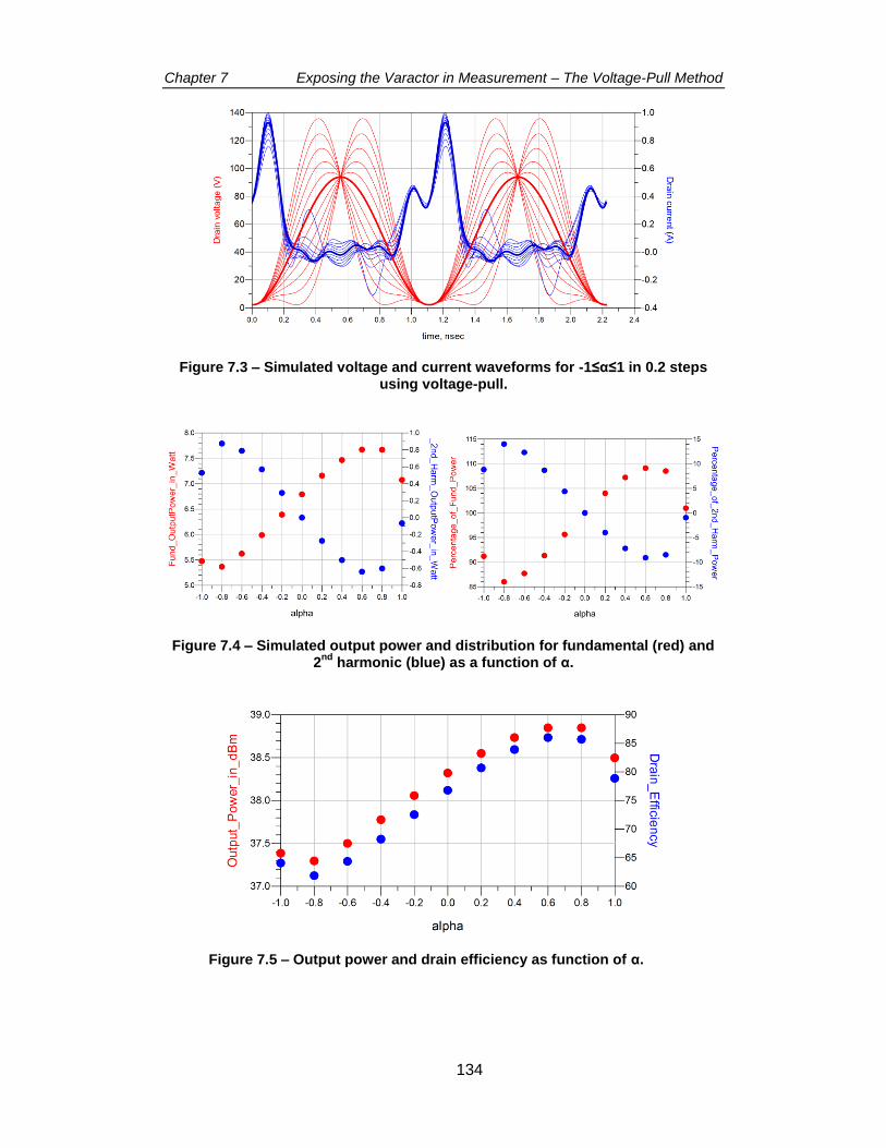
Chapter 7 Exposing the Varactor in Measurement – The Voltage-Pull Method
134
Figure 7.3 – Simulated voltage and current waveforms for -1≤α≤1 in 0.2 steps using voltage-pull.
Figure 7.4 – Simulated output power and distribution for fundamental (red) and 2
nd harmonic (blue) as a function of α.
Figure 7.5 – Output power and drain efficiency as function of α.

Chapter 7 Exposing the Varactor in Measurement – The Voltage-Pull Method
135
The output power and drain efficiency as a function of α are shown in
Fig. 7.5. As a result of the energy up-conversion in the negative α region, the
device output power and efficiency dropped in performance compared to the
reference class-B (α=0) case by as much as 15%. In contrast, the output
power and efficiency improved by as much as 10% in the positive α region as
the energy from the 2nd harmonic was injected and down-converted to
fundamental, as predicted from the mathematical analysis.
7.3.3 Simulating an Applied Phase Shift on the Output Voltage
The next step was to simulate the necessary phase shift on the output
voltage at each α value to bring the 2nd harmonic loads to the edge of the
Smith chart, as performed in the mathematical analysis in Chapter 6. In this
example simulation, the required phase shift for each α was manually obtained
using the ADS Tuning function.
Fig. 7.6 shows the phase shift values that were applied and the
modified fundamental and 2nd harmonic load trajectories, which agreed with the
trajectories predicted from the mathematical analysis in Fig. 6.13.
The resulting output power from simulation after phase shift was
applied is shown in Fig. 7.7. It is observed that the energy conversion from the
varactor was not as large as the one from the mathematical analysis. This is
because this simulation took into account the device knee voltage and this also
reduced the CDS variation.

Chapter 7 Exposing the Varactor in Measurement – The Voltage-Pull Method
136
Figure 7.6 - Required phase shift obtained manually from the ADS Tuning function (top) and the resulting modified load trajectories (bottom).
Figure 7.7 - Simulated output power with phase shift applied.
The simulated output power and drain efficiency comparison before and
after applying phase shift are shown in Fig. 7.8. The efficiency in the positive α
region decreased as the 2nd harmonic injection effect was removed when the
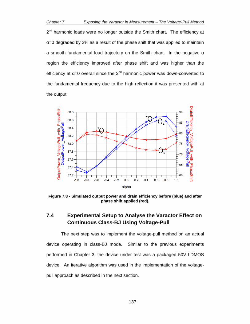
Chapter 7 Exposing the Varactor in Measurement – The Voltage-Pull Method
137
2nd harmonic loads were no longer outside the Smith chart. The efficiency at
α=0 degraded by 2% as a result of the phase shift that was applied to maintain
a smooth fundamental load trajectory on the Smith chart. In the negative α
region the efficiency improved after phase shift and was higher than the
efficiency at α=0 overall since the 2nd harmonic power was down-converted to
the fundamental frequency due to the high reflection it was presented with at
the output.
Figure 7.8 - Simulated output power and drain efficiency before (blue) and after phase shift applied (red).
7.4 Experimental Setup to Analyse the Varactor Effect on
Continuous Class-BJ Using Voltage-Pull
The next step was to implement the voltage-pull method on an actual
device operating in class-BJ mode. Similar to the previous experiments
performed in Chapter 3, the device under test was a packaged 50V LDMOS
device. An iterative algorithm was used in the implementation of the voltage-
pull approach as described in the next section.

Chapter 7 Exposing the Varactor in Measurement – The Voltage-Pull Method
138
7.4.1 Voltage-Pull Experimental Setup
The same active load-pull system was used in this experiment but
instead of executing the usual load-pull characterisation, the waveform
engineering system was now configured to run voltage-pull instead. The
device was biased in continuous class-BJ mode at 900MHz near the maximum
drain bias point of 48V to enable a more visible energy transfer between
fundamental and 2nd harmonic. The fundamental load that produced maximum
efficiency at 48V bias (150Ω) was selected so that any further increase in
efficiency can be attributed to the varactor’s 2nd harmonic energy down-
conversion. A class-B mode (α=0 state) was used as a reference state for the
rest of the α values. The drive level at each α was adjusted to maintain a
constant DC current as the class-B state.
7.4.2 Implementing Voltage-Pull Method Using an Active Load-Pull
System
The Mesuro active load-pull system at Cardiff University uses a load
search algorithm, targeting loads instead of voltage waveforms. The
fundamental and harmonic loads are synthesized based on the measured
incident and reflected waves using external signal generators. Since it is an
active load-pull system, it is able to synthesize negative loads, which allows for
this varactor analysis. However, the Mesuro system is unable to perform
voltage-pull directly on its own. In order to use this system for voltage-pull,
additional steps are needed to report the loads that correspond to the desired
voltage waveforms, and for this work the ADS software was used to provide
this function, as shown in Fig. 7.9.
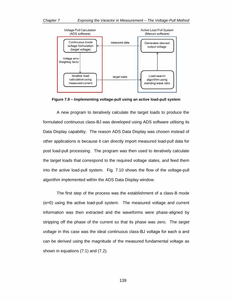
Chapter 7 Exposing the Varactor in Measurement – The Voltage-Pull Method
139
Figure 7.9 – Implementing voltage-pull using an active load-pull system
A new program to iteratively calculate the target loads to produce the
formulated continuous class-BJ was developed using ADS software utilising its
Data Display capability. The reason ADS Data Display was chosen instead of
other applications is because it can directly import measured load-pull data for
post load-pull processing. The program was then used to iteratively calculate
the target loads that correspond to the required voltage states, and feed them
into the active load-pull system. Fig. 7.10 shows the flow of the voltage-pull
algorithm implemented within the ADS Data Display window.
The first step of the process was the establishment of a class-B mode
(α=0) using the active load-pull system. The measured voltage and current
information was then extracted and the waveforms were phase-aligned by
stripping off the phase of the current so that its phase was zero. The target
voltage in this case was the ideal continuous class-BJ voltage for each α and
can be derived using the magnitude of the measured fundamental voltage as
shown in equations (7.1) and (7.2).

Chapter 7 Exposing the Varactor in Measurement – The Voltage-Pull Method
140
Figure 7.10 – Voltage pull algorithm flow
𝑉𝑡𝑎𝑟𝑔𝑒𝑡_𝑓0 = 𝑉𝐵𝐽_𝑓0 = −|𝑉𝑓0| + 𝑗𝛼|𝑉𝑓0| (7.1)
𝑉𝑡𝑎𝑟𝑔𝑒𝑡_2𝑓0 = 𝑉𝐵𝐽_2𝑓0 = 0 − 𝑗1
2𝛼|𝑉𝑓0| (7.2)
Using the measured current, the target load for each frequency
component can be calculated using the equation:
𝑍𝑡𝑎𝑟𝑔𝑒𝑡 =𝑉𝑡𝑎𝑟𝑔𝑡
𝐼𝑚𝑒𝑎𝑠𝑢𝑟𝑒𝑑
(7.3)
The calculated fundamental and harmonic loads for each α were then
fed into the active load-pull system, which used external signal generators to
produce the next iteration of voltage waveform. The difference between the
resulting voltage (Fig. 7.11) and the ideal class-BJ voltage, or the error voltage
EV, can be calculated as:
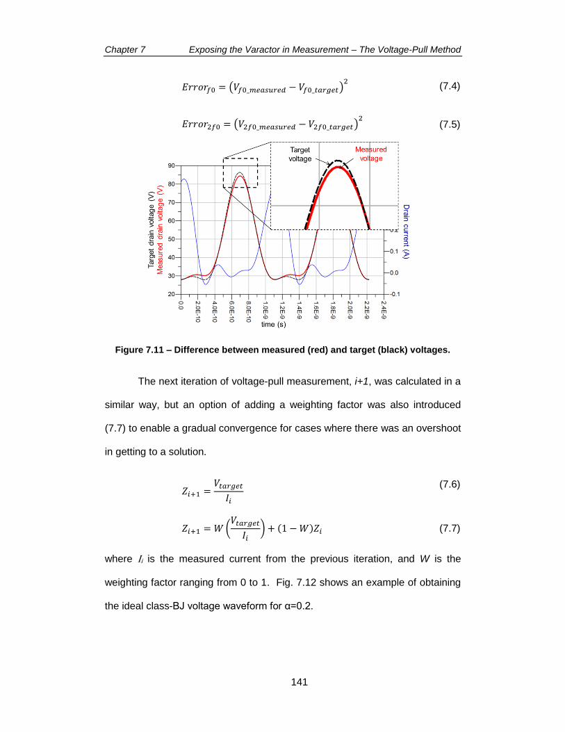
Chapter 7 Exposing the Varactor in Measurement – The Voltage-Pull Method
141
𝐸𝑟𝑟𝑜𝑟𝑓0 = (𝑉𝑓0_𝑚𝑒𝑎𝑠𝑢𝑟𝑒𝑑 − 𝑉𝑓0_𝑡𝑎𝑟𝑔𝑒𝑡)2 (7.4)
𝐸𝑟𝑟𝑜𝑟2𝑓0 = (𝑉2𝑓0_𝑚𝑒𝑎𝑠𝑢𝑟𝑒𝑑 − 𝑉2𝑓0_𝑡𝑎𝑟𝑔𝑒𝑡)2 (7.5)
Figure 7.11 – Difference between measured (red) and target (black) voltages.
The next iteration of voltage-pull measurement, i+1, was calculated in a
similar way, but an option of adding a weighting factor was also introduced
(7.7) to enable a gradual convergence for cases where there was an overshoot
in getting to a solution.
𝑍𝑖+1 =𝑉𝑡𝑎𝑟𝑔𝑒𝑡
𝐼𝑖
(7.6)
𝑍𝑖+1 = 𝑊 (𝑉𝑡𝑎𝑟𝑔𝑒𝑡
𝐼𝑖) + (1 − 𝑊)𝑍𝑖 (7.7)
where Ii is the measured current from the previous iteration, and W is the
weighting factor ranging from 0 to 1. Fig. 7.12 shows an example of obtaining
the ideal class-BJ voltage waveform for α=0.2.

Chapter 7 Exposing the Varactor in Measurement – The Voltage-Pull Method
142
Figure 7.12 - Iteration example for α=0.2.
The weighting factor was only needed in some of the iterations as they
converged closer to the final solution. Throughout the voltage-pull iteration
process, the drive level was adjusted such that the DC current component
remained constant. This was to ensure that a proper baselining was done.
The peak current value IMAX in this case could not be used as a reference in
setting the drive level because it changes due to the displacement current from
the nonlinear CDS.
7.5 Voltage-Pull Measurement Results & Discussions
The voltage-pull measurement was first performed at a low input drive
level to stay within the linear region and also to reduce the device CDS
variation. The purpose of this step was not to analyse the output power and
efficiency performance but to verify the algorithm developed in Section 7.4 on
a real device. The same step was also performed in simulation for
comparison.

Chapter 7 Exposing the Varactor in Measurement – The Voltage-Pull Method
143
In the second part of the experiment the device was driven
approximately 1dB into compression exercising the full range of the CDS-VDS
nonlinear relationship to enable device performance analysis.
7.5.1 Verifying the Voltage-Pull Method Using Low Input Drive Level
Fig. 7.13 shows the simulated and measured voltage and current
waveforms obtained from the voltage-pull method as well as the load
trajectories when performed at a low drive level without hitting the knee region
for -1≤α≤1 in 0.2 steps. For this small voltage swing the variation in CDS was
relatively small and the peak drain current did not vary significantly with α.
There are several observations that can be made from this step. Firstly
the voltage waveforms obtained from measurement were close to the ideal
continuous class-BJ mode waveform which verified that the voltage-pull
approach using an active load-pull system worked well in setting up an ideal
continuous class-BJ mode. Secondly there was a good correlation between
simulated and measured waveforms, providing a high confidence on the
device model and simulation results.
However it was also observed that to obtain these ideal class-BJ
voltage waveforms in measurement the 2nd harmonic load trajectory stays
outside the Smith chart for -1≤α≤0, unlike in simulation where the 2nd harmonic
load enters inside the Smith chart, upholding the varactor effect even at this
low drive level. The measurement results indicate possibly a resistive loss at
the output after the device current generator plane for the real device which
cancelled out the effect of the varactor observed in simulation and from the
mathematical analysis in Chapter 6. This was the main discrepancy observed
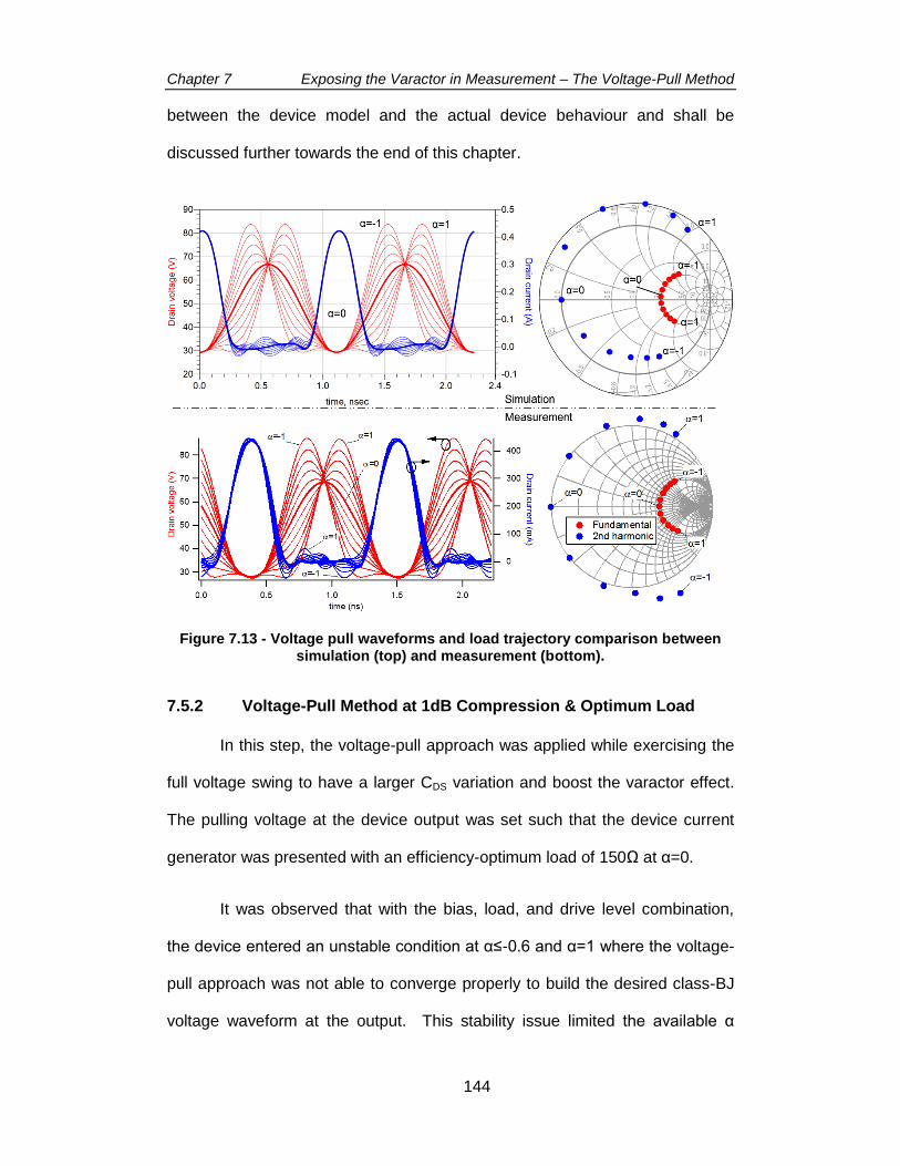
Chapter 7 Exposing the Varactor in Measurement – The Voltage-Pull Method
144
between the device model and the actual device behaviour and shall be
discussed further towards the end of this chapter.
Figure 7.13 - Voltage pull waveforms and load trajectory comparison between simulation (top) and measurement (bottom).
7.5.2 Voltage-Pull Method at 1dB Compression & Optimum Load
In this step, the voltage-pull approach was applied while exercising the
full voltage swing to have a larger CDS variation and boost the varactor effect.
The pulling voltage at the device output was set such that the device current
generator was presented with an efficiency-optimum load of 150Ω at α=0.
It was observed that with the bias, load, and drive level combination,
the device entered an unstable condition at α≤-0.6 and α=1 where the voltage-
pull approach was not able to converge properly to build the desired class-BJ
voltage waveform at the output. This stability issue limited the available α
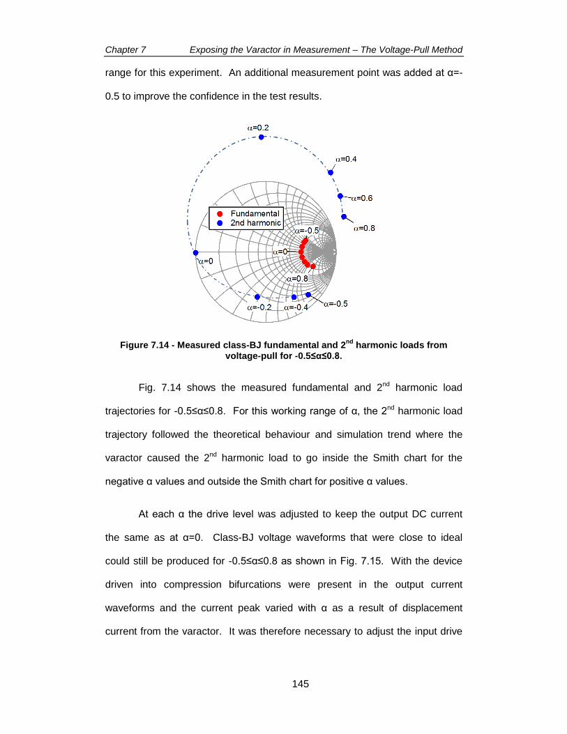
Chapter 7 Exposing the Varactor in Measurement – The Voltage-Pull Method
145
range for this experiment. An additional measurement point was added at α=-
0.5 to improve the confidence in the test results.
Figure 7.14 - Measured class-BJ fundamental and 2nd
harmonic loads from voltage-pull for -0.5≤α≤0.8.
Fig. 7.14 shows the measured fundamental and 2nd harmonic load
trajectories for -0.5≤α≤0.8. For this working range of α, the 2nd harmonic load
trajectory followed the theoretical behaviour and simulation trend where the
varactor caused the 2nd harmonic load to go inside the Smith chart for the
negative α values and outside the Smith chart for positive α values.
At each α the drive level was adjusted to keep the output DC current
the same as at α=0. Class-BJ voltage waveforms that were close to ideal
could still be produced for -0.5≤α≤0.8 as shown in Fig. 7.15. With the device
driven into compression bifurcations were present in the output current
waveforms and the current peak varied with α as a result of displacement
current from the varactor. It was therefore necessary to adjust the input drive
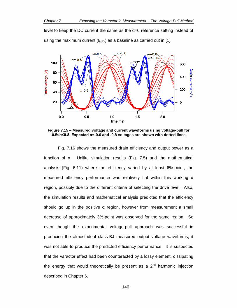
Chapter 7 Exposing the Varactor in Measurement – The Voltage-Pull Method
146
level to keep the DC current the same as the α=0 reference setting instead of
using the maximum current (IMAX) as a baseline as carried out in [1].
Figure 7.15 – Measured voltage and current waveforms using voltage-pull for -0.5≤α≤0.8. Expected α=-0.6 and -0.8 voltages are shown with dotted lines.
Fig. 7.16 shows the measured drain efficiency and output power as a
function of α. Unlike simulation results (Fig. 7.5) and the mathematical
analysis (Fig. 6.11) where the efficiency varied by at least 6%-point, the
measured efficiency performance was relatively flat within this working α
region, possibly due to the different criteria of selecting the drive level. Also,
the simulation results and mathematical analysis predicted that the efficiency
should go up in the positive α region, however from measurement a small
decrease of approximately 3%-point was observed for the same region. So
even though the experimental voltage-pull approach was successful in
producing the almost-ideal class-BJ measured output voltage waveforms, it
was not able to produce the predicted efficiency performance. It is suspected
that the varactor effect had been counteracted by a lossy element, dissipating
the energy that would theoretically be present as a 2nd harmonic injection
described in Chapter 6.

Chapter 7 Exposing the Varactor in Measurement – The Voltage-Pull Method
147
The next step of the investigation was to apply a phase shift to the
output voltage and bring the 2nd harmonic loads that were inside the Smith
chart in Fig. 7.14 (in the negative α region) towards the edge and recover the
efficiency.
Figure 7.16 – Measured output power and drain efficiency from voltage-pull.
7.5.3 Applying Phase Shift on the Output Voltage
The objective of this section is to find out if it is possible to practically
exploit the varactor and use it to improve efficiency performance in the
negative α region. As demonstrated in simulation and in the mathematical
analysis, an improvement in efficiency can be obtained by pushing the 2nd
harmonic loads that are inside the Smith chart towards the edge. From the
results obtained in Fig. 7.14 this was only applicable for α values of -0.2, -0.4,
and -0.5.
Applying phase shift for each α required a slightly modified algorithm
from the flow described in Fig. 7.10. ADS software was used to estimate the
initial required phase shift which was then set as the target voltage waveform.
The voltage-pull method was then executed to construct this waveform on the
device output. If the resulting 2nd harmonic load did not sit on the edge of the
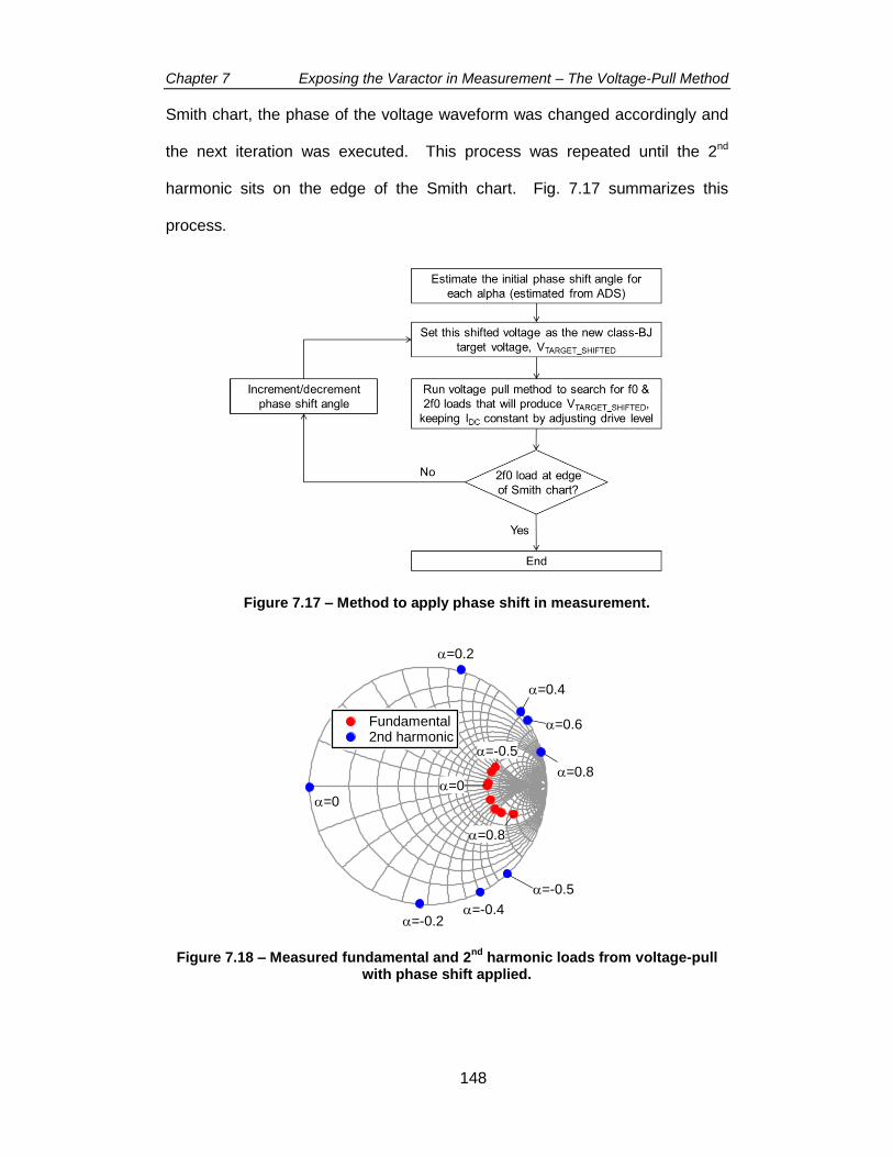
Chapter 7 Exposing the Varactor in Measurement – The Voltage-Pull Method
148
Smith chart, the phase of the voltage waveform was changed accordingly and
the next iteration was executed. This process was repeated until the 2nd
harmonic sits on the edge of the Smith chart. Fig. 7.17 summarizes this
process.
Figure 7.17 – Method to apply phase shift in measurement.
Figure 7.18 – Measured fundamental and 2nd
harmonic loads from voltage-pull with phase shift applied.
1.5
1.0
0.5
0.0
-0.5
-1.0
1.51.00.50.0-0.5-1.0
Fundamental 2nd harmonic
=-0.5
=0.8
=0.4
=0
=-0.5
=-0.4
=0
=0.2
=0.6
=0.8
=-0.2

Chapter 7 Exposing the Varactor in Measurement – The Voltage-Pull Method
149
The resulting measured fundamental and 2nd harmonic load trajectories
with phase shift applied are shown in Fig. 7.18, for the applicable range of
-0.5≤α≤0.8 in 0.2 steps. In this example, the phase shift was not applied at
α=0.
Fig. 7.19 shows the measured output power and drain efficiency
comparison before and after applying phase shift. A small improvement of 3%-
point and 2%-point was observed at α=-0.4 and -0.5, respectively. This
amount was small compared to prediction from simulation and mathematical
analysis which again was likely to be caused by the lossy element of the
varactor. As expected, the drain efficiency dropped in the positive α region
with the removal of the 2nd harmonic injection effect provided by the varactor.
The small improvement seen at the negative α region can be traced to
the distribution of fundamental and 2nd harmonic power before the phase shift,
as shown in Fig. 7.20. Before applying phase shift the split between
fundamental and 2nd harmonic power was only ± 2% at best, compared to
simulation (± 15%) and mathematical analysis (± 8%).
Figure 7.19 – Measured output power and drain efficiency before and after phase shifting.
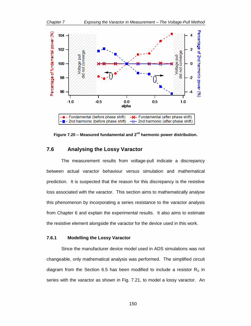
Chapter 7 Exposing the Varactor in Measurement – The Voltage-Pull Method
150
Figure 7.20 – Measured fundamental and 2nd
harmonic power distribution.
7.6 Analysing the Lossy Varactor
The measurement results from voltage-pull indicate a discrepancy
between actual varactor behaviour versus simulation and mathematical
prediction. It is suspected that the reason for this discrepancy is the resistive
loss associated with the varactor. This section aims to mathematically analyse
this phenomenon by incorporating a series resistance to the varactor analysis
from Chapter 6 and explain the experimental results. It also aims to estimate
the resistive element alongside the varactor for the device used in this work.
7.6.1 Modelling the Lossy Varactor
Since the manufacturer device model used in ADS simulations was not
changeable, only mathematical analysis was performed. The simplified circuit
diagram from the Section 6.5 has been modified to include a resistor RS in
series with the varactor as shown in Fig. 7.21, to model a lossy varactor. An
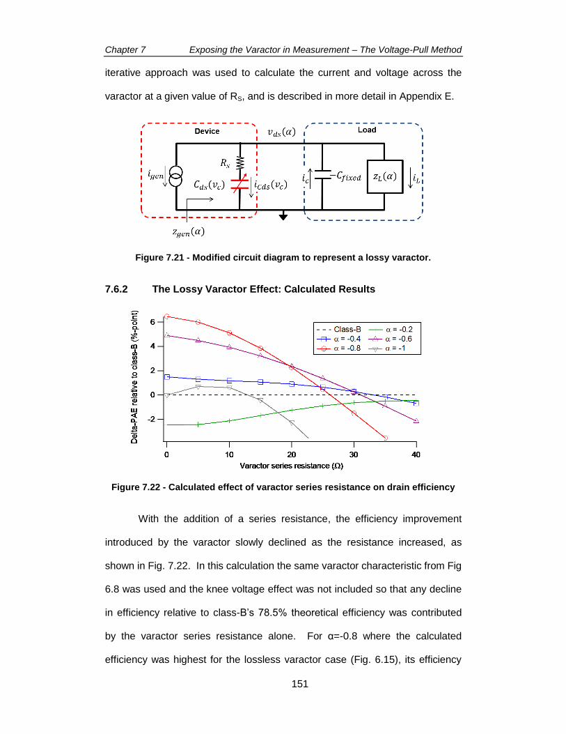
Chapter 7 Exposing the Varactor in Measurement – The Voltage-Pull Method
151
iterative approach was used to calculate the current and voltage across the
varactor at a given value of RS, and is described in more detail in Appendix E.
Figure 7.21 - Modified circuit diagram to represent a lossy varactor.
7.6.2 The Lossy Varactor Effect: Calculated Results
Figure 7.22 - Calculated effect of varactor series resistance on drain efficiency
With the addition of a series resistance, the efficiency improvement
introduced by the varactor slowly declined as the resistance increased, as
shown in Fig. 7.22. In this calculation the same varactor characteristic from Fig
6.8 was used and the knee voltage effect was not included so that any decline
in efficiency relative to class-B’s 78.5% theoretical efficiency was contributed
by the varactor series resistance alone. For α=-0.8 where the calculated
efficiency was highest for the lossless varactor case (Fig. 6.15), its efficiency
Chapter 7 Exposing the Varactor in Measurement – The Voltage-Pull Method
152
benefit was fully counteracted by a series resistance of approximately 27Ω.
Overall, the calculated efficiency benefit for all α was completely diminished by
a series resistance higher than 34Ω when the knee voltage effect was not
included.
7.6.3 Estimating the Varactor Series Resistance of the Actual Device
In order to estimate the series resistance of the device used in Section
7.5, the varactor and device parameters were modified to reflect its actual
behaviour instead of using ideal parameters. From Fig. 7.15 the knee voltage
can be estimated to be 6V while the DC bias and voltage swing are 48V and
42V, respectively. The measured DC current of 195mA was used to determine
the drain current magnitude.
With the knee voltage factor applied, the calculated class-B drain
efficiency dropped to from 78.5% to 69% without any varactor series resistance
(RS=0Ω). The measured efficiency of 65% corresponds to a calculated
efficiency performance with a varactor series resistance of 9Ω. This was the
step used to estimate the varactor series resistance for the rest of α, which is
summarized in Fig. 7.23.
From Fig. 7.23 there were some differences in the estimated series
resistance before and after phase shift was applied. This could be attributed to
the measurement uncertainty from the active load-pull setup and the accuracy
of the fixed de-embedding value used. Even the CDS model itself was subject
to uncertainty as a result of simplification techniques [2].
It was observed from this basic analysis that the varactor series
resistance RS was not constant throughout the different α values in this class-
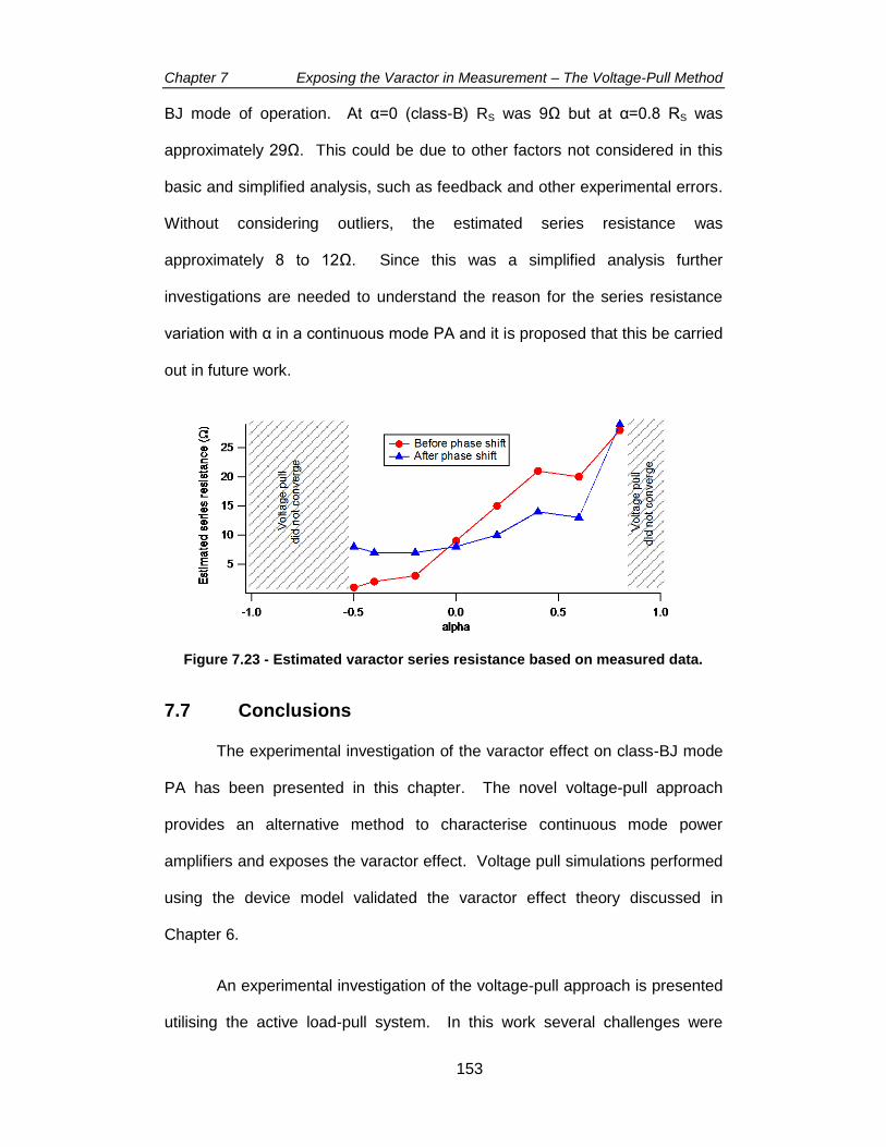
Chapter 7 Exposing the Varactor in Measurement – The Voltage-Pull Method
153
BJ mode of operation. At α=0 (class-B) RS was 9Ω but at α=0.8 RS was
approximately 29Ω. This could be due to other factors not considered in this
basic and simplified analysis, such as feedback and other experimental errors.
Without considering outliers, the estimated series resistance was
approximately 8 to 12Ω. Since this was a simplified analysis further
investigations are needed to understand the reason for the series resistance
variation with α in a continuous mode PA and it is proposed that this be carried
out in future work.
Figure 7.23 - Estimated varactor series resistance based on measured data.
7.7 Conclusions
The experimental investigation of the varactor effect on class-BJ mode
PA has been presented in this chapter. The novel voltage-pull approach
provides an alternative method to characterise continuous mode power
amplifiers and exposes the varactor effect. Voltage pull simulations performed
using the device model validated the varactor effect theory discussed in
Chapter 6.
An experimental investigation of the voltage-pull approach is presented
utilising the active load-pull system. In this work several challenges were
Chapter 7 Exposing the Varactor in Measurement – The Voltage-Pull Method
154
encountered in its implementation. The first challenge was providing high
enough fundamental and 2nd harmonic injected power at the device output in
order to formulate the desired output voltage. Secondly a device stability issue
was also encountered, most likely due to the fact that the device used for this
work was a ‘test device’ packaged specifically for this PhD work. This test
device did not have the proper output-input feedback isolation internally as do
the standard ones.
The theory of exploiting the varactor for drain efficiency enhancement,
although showing potential in the mathematical analysis and simulation, was
limited in the measured results, possibly due to the resistive loss of the
varactor. A maximum of 3% improvement was obtained from voltage-pull
measurement at α=-0.4. This number could possibly be further improved using
different CDS-VDS characteristics than the one used in this work, and this
extended investigation can be included in future work.
Finally it is also proposed that this this research be extended onto other
device technologies such as Gallium Nitride (GaN) which is currently gaining
traction in the mobile communication systems [3].
7.8 References
[1] V. Carrubba, "Novel highly efficient broadband continuous power amplifier modes," PhD Thesis, Cardiff University, 2012.
[2] P. Aaen, Jaime A. Plá, and J. Wood., Modeling and Characterization of RF and Microwave Power FETs: Cambridge University Press, 2007.
[3] S. C. Cripps, RF Power Amplifiers for Wireless Communications: Artech House, 2006.
Chapter 8 Conclusions & Future Work
155
Chapter 8 Conclusions & Future Work
8.1 Conclusions
Maximizing the system-level efficiency performance of an envelope
tracking (ET) power amplifier system requires both the envelope amplifier and
the RF power amplifier to be highly efficient. However, in previous ET system
designs, less attention has been given to the RF power amplifier [1] and the
class-AB mode RF PA has been the common choice for implementation [2].
This research work fills that gap and provides a systematic analysis on the use
of higher-efficiency RF PA modes, and specifically in this work, class-F in ET
system applications. This chapter discusses and concludes the five objectives
listed in Chapter 1 for this research.
The novel use of waveform engineering in analysing any PA mode for
envelope tracking applications has been described, revealing the challenge of
maintaining a particular high-efficiency mode such as class-F throughout the
entire ET supply range, due to the nonlinear CDS variation. This analysis
uncovers the maximum available efficiency of class-F and class-AB modes in
ET as well as the predicted efficiency when the PA load impedances are
optimised at any given bias point. The effect of CDS on the optimum load at
different bias and the resulting load trajectory have been demonstrated for
class-F and class-AB using a 50V high voltage LDMOS device. For class-F, it
was shown that optimising the loads at 28V improved the efficiency at 7.5dB
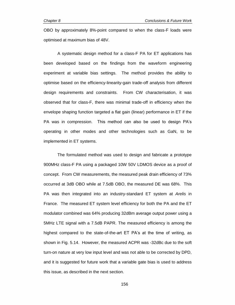
Chapter 8 Conclusions & Future Work
156
OBO by approximately 8%-point compared to when the class-F loads were
optimised at maximum bias of 48V.
A systematic design method for a class-F PA for ET applications has
been developed based on the findings from the waveform engineering
experiment at variable bias settings. The method provides the ability to
optimise based on the efficiency-linearity-gain trade-off analysis from different
design requirements and constraints. From CW characterisation, it was
observed that for class-F, there was minimal trade-off in efficiency when the
envelope shaping function targeted a flat gain (linear) performance in ET if the
PA was in compression. This method can also be used to design PA’s
operating in other modes and other technologies such as GaN, to be
implemented in ET systems.
The formulated method was used to design and fabricate a prototype
900MHz class-F PA using a packaged 10W 50V LDMOS device as a proof of
concept. From CW measurements, the measured peak drain efficiency of 73%
occurred at 3dB OBO while at 7.5dB OBO, the measured DE was 68%. This
PA was then integrated into an industry-standard ET system at Arelis in
France. The measured ET system level efficiency for both the PA and the ET
modulator combined was 64% producing 32dBm average output power using a
5MHz LTE signal with a 7.5dB PAPR. The measured efficiency is among the
highest compared to the state-of-the-art ET PA’s at the time of writing, as
shown in Fig. 5.14. However, the measured ACPR was -32dBc due to the soft
turn-on nature at very low input level and was not able to be corrected by DPD,
and it is suggested for future work that a variable gate bias is used to address
this issue, as described in the next section.

Chapter 8 Conclusions & Future Work
157
The use of ET as a baseband linearisation method has also been
explored in addition to improving efficiency. The ET flat-gain shaping function
for a linear performance consisted of a 2nd-order term which agreed with the
findings from [3]. Therefore it can be concluded that the baseband signal
injection at the drain has the potential to be implemented as an envelope
shaping function in ET systems, but its effectiveness in reducing AM-AM
distortion is limited when used with a class-F mode PA due to the soft turn-on
characteristics which resulted from a class-B biasing. A different outcome can
be expected if a class-F-1 is used, for example with GaN technology.
The use of a continuous class-F PA mode in a variable drain bias has
been demonstrated using waveform engineering, and it highlighted the positive
and negative effects of the nonlinear output capacitance, or the varactor, on
the PA efficiency performance even at a single bias. These findings led to the
development of a novel method to characterise continuous mode PA’s called
voltage-pull, enabling a new design space to be explored. From mathematical
analysis and simulation results, it was observed that there is a possibility to
exploit the varactor as a 2nd harmonic injection source to improve efficiency.
However, the measured results did not achieve the level of improvement
predicted and it is suspected that it was due to the varactor having an
associated resistive loss. Although the experimental efficiency improvement
from this approach was minimal compared to simulation, the outcome of this
study can be used for future work in this topic, and may well be more relevant
to other device technologies.
While the envelope tracking architecture is getting more attention as the
demand for bandwidth and efficiency increases, it is currently more widely
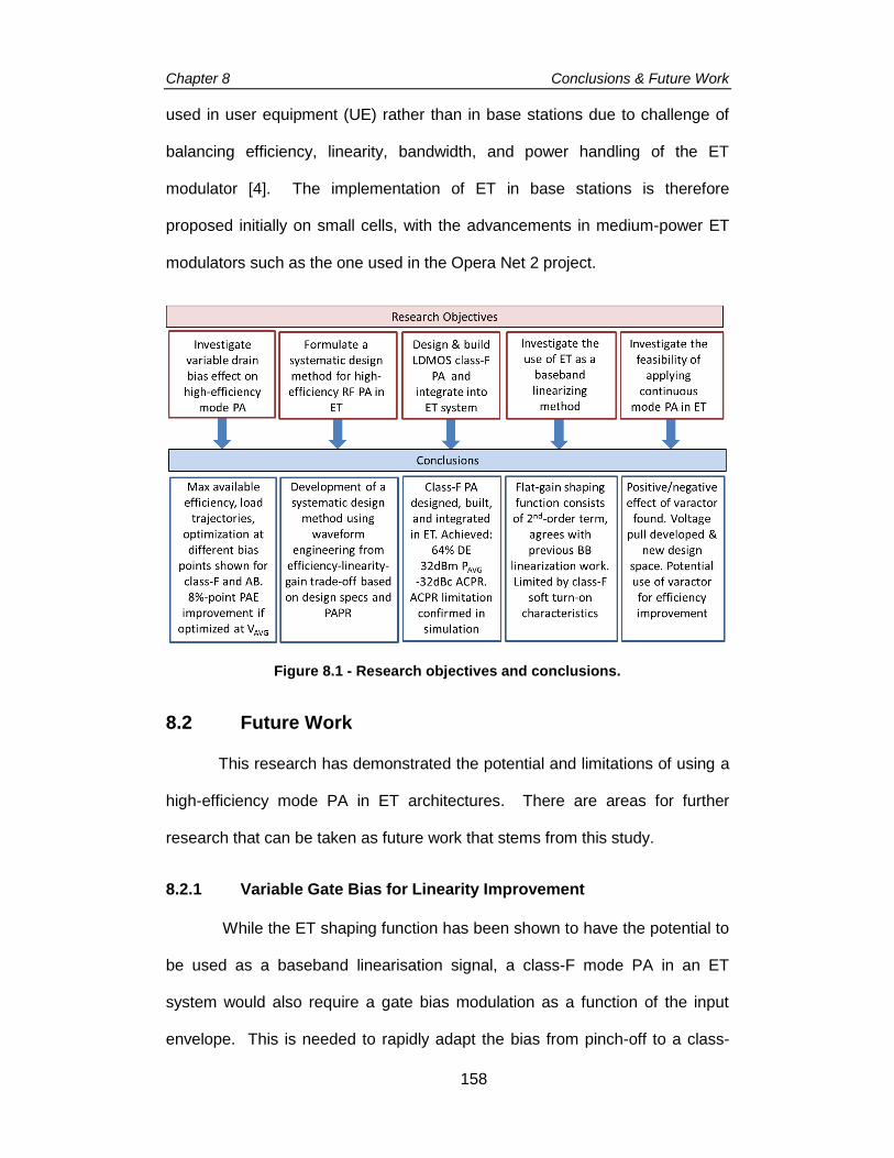
Chapter 8 Conclusions & Future Work
158
used in user equipment (UE) rather than in base stations due to challenge of
balancing efficiency, linearity, bandwidth, and power handling of the ET
modulator [4]. The implementation of ET in base stations is therefore
proposed initially on small cells, with the advancements in medium-power ET
modulators such as the one used in the Opera Net 2 project.
Figure 8.1 - Research objectives and conclusions.
8.2 Future Work
This research has demonstrated the potential and limitations of using a
high-efficiency mode PA in ET architectures. There are areas for further
research that can be taken as future work that stems from this study.
8.2.1 Variable Gate Bias for Linearity Improvement
While the ET shaping function has been shown to have the potential to
be used as a baseband linearisation signal, a class-F mode PA in an ET
system would also require a gate bias modulation as a function of the input
envelope. This is needed to rapidly adapt the bias from pinch-off to a class-
Chapter 8 Conclusions & Future Work
159
AB-like bias at very low drive levels, trading-off a small enough efficiency to
meet the linearity requirement. Fig. 8.2 shows some simulated results that
illustrate the potential of linearising the device transconductance while
maintaining high efficiency by varying both gate and drain bias voltages of a
class-F mode PA under a 2-tone excitation. Further work is required in
defining this ‘gate bias shaping function’ and aligning it with the drain
modulation.
Fig 8.2 - The effect of varying only the drain bias (left) and varying both drain and gate bias (right) on the linearity of the transconductance curve.
8.2.2 Further Shaping Function Adjustment and Optimisation in an
ET Test Environment
In Chapter 5, the ET system level test was performed using shaping
functions that would ideally replicate the ‘flat-gain’ and ‘max-PAE’ shaping
functions defined in Chapter 4. However, the shaping function entry at the ET
system level was done in the digital domain using digital-to-analogue
converters (DAC), causing a level of uncertainty in the exact replication of the
desired shaping functions.
Furthermore, the desired shaping functions were extracted from CW
measurements using a fixture that was de-embedded to the current generator
plane. At the PA level and in an ET integrated system, the input and output

Chapter 8 Conclusions & Future Work
160
characteristics have changed and this potentially will affect the shaping
function accuracy. Ideally a different setup is needed which would have the
ability to automatically search for a constant gain criteria and generate a new
shaping function in situ. Such a system would have a controllable DC supply
which would take the place of an ET drain modulator. Having this capability
allows for a more accurate shaping function generation and deployment.
8.2.3 Using GaN Technology in Inverse Class-F Mode for Potential
Incremental Efficiency and Linearity Improvement
GaN technology has a smaller on-resistance (RON) compared to
LDMOS and a smaller output capacitance. These characteristics potentially
could produce a higher baseline drain efficiency compared to LDMOS as seen
in [5]. Using a GaN device also would enable the inverse class-F mode which
theoretically would avoid the linearity issue caused by the soft turn-on
phenomenon seen in class-F mode PA’s. The class-F-1 mode was not
possible to be implemented in this research due to the large CDS associated
with LDMOS technology, making it difficult to present an open circuit at the 2nd
harmonic through active load-pull.
8.2.4 Automating the Voltage-Pull Method for Continuous Mode PA
Characterisation
The voltage-pull method described in Chapter 7 was performed
manually, toggling between the active load-pull system and the load calculation
template in ADS in several iterations. The iteration process could be made
faster through automation by merging the two functions (load calculation and
load-pulling) into one user interface.

Chapter 8 Conclusions & Future Work
161
There was also an issue with regards to stability of the device which
prevented a full characterisation of the continuous mode in Chapter 7. A
comprehensive stability analysis is therefore needed to address this issue for a
fully functional voltage-pull test setup.
8.2.5 Further Research into the Varactor for Effect on Continuous
Mode PA’s and Potential Use for Efficiency Enhancement
The mathematical analysis shown in Chapter 6 indicated a possibility of
exploiting the varactor for efficiency enhancement, but this was limited in the
actual device. This research predicted that the lossy element of the varactor
contributed to this discrepancy. However it is also noted that the mathematical
analysis performed in Chapters 6 and 7 is a simplified analysis and there could
be other factors involved, which were not included such as the input
capacitance effect. The measurement results could also inherently have a
larger uncertainty than expected as a result of de-embedding inaccuracies.
Further research is needed to understand the discrepancies between the
predicted and the actual device performance, as well as investigating optimum
CDS-VDS characteristics that would enlarge the varactor effect for a potentially
larger efficiency improvement.
8.3 References
[1] G. F. Collins, J. Fisher, F. Radulescu, J. Barner, S. Sheppard, R. Worley, et al., "Power Amplifier Design Optimized for Envelope Tracking," in Compound Semiconductor Integrated Circuit Symposium (CSICs), 2014 IEEE, 2014, pp. 1-4.
[2] K. Bumman, M. Junghwan, and K. Ildu, "Efficiently Amplified," Microwave Magazine, IEEE, vol. 11, pp. 87-100, 2010.
[3] F. L. Ogboi, P. J. Tasker, M. Akmal, J. Lees, J. Benedikt, S. Bensmida, et al., "A LSNA configured to perform baseband engineering for device

Chapter 8 Conclusions & Future Work
162
linearity investigations under modulated excitations," in Microwave Conference (EuMC), 2013 European, 2013, pp. 684-687.
[4] Z. Wang, Envelope Tracking Power Amplifiers for Wireless Communications: Artech House, 2014.
[5] P. Wright, A. Sheikh, C. Roff, P. J. Tasker, and J. Benedikt, "Highly efficient operation modes in GaN power transistors delivering upwards of 81% efficiency and 12W output power," in Microwave Symposium Digest, 2008 IEEE MTT-S International, 2008, pp. 1147-1150.

Appendix A Measurement Setup
163
Appendix A Measurement Setup
Active Load-Pull System and Waveform Engineering A.1 Measurement Setup
The waveform engineering approach uses an active load-pull system to
construct the desired current and voltage waveforms at the transistor current
generator plane. It is achieved by synthesizing the required fundamental and
harmonic loads at any bias point hence setting up any PA mode of operation,
emulating a harmonic balance simulation in actual measurement.
The voltage and current waveform measurements are performed using
a measurement system based around an Agilent N5242A PNA-X Nonlinear
Vector Network Analyser (NVNA) as the receiver. It can measure up to
26.5GHz but for this work the fundamental frequency is set at 900MHz. Three
signal generators together with their associated power amplifiers are used to
synthesize the travelling fundamental and harmonic waves incident on the
output of the device, setting up the fundamental and harmonic load conditions
up to the third harmonic as shown in Fig. A.1. A triplexer is used to combine
the 3 harmonics into 1 path, placed between the device and the load-pull
signal generators. The input signal is a 900MHz continuous wave (CW) signal
generated by an RF signal generator with a driver amplifier. No input matching
is applied on the device input side in this research work, instead the input drive
level is increased accordingly to overcome the mismatch losses to arrive at the
desired input power level.
External directional couplers are used to sample the incident and
reflected waves on both sides of the device to the PNA-X receiver channels.
The PNA-X ports 1 and 2 are used for the device under test (DUT) while ports
3 and 4 are used to connect the phase reference modules which enable the
nonlinear measurements by correlating the relative phase of the harmonics.
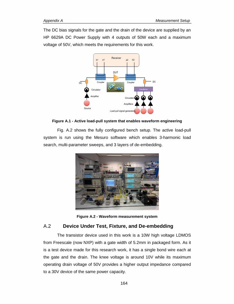
Appendix A Measurement Setup
164
The DC bias signals for the gate and the drain of the device are supplied by an
HP 6629A DC Power Supply with 4 outputs of 50W each and a maximum
voltage of 50V, which meets the requirements for this work.
Figure A.1 - Active load-pull system that enables waveform engineering
Fig. A.2 shows the fully configured bench setup. The active load-pull
system is run using the Mesuro software which enables 3-harmonic load
search, multi-parameter sweeps, and 3 layers of de-embedding.
Figure A.2 - Waveform measurement system
Device Under Test, Fixture, and De-embedding A.2
The transistor device used in this work is a 10W high voltage LDMOS
from Freescale (now NXP) with a gate width of 5.2mm in packaged form. As it
is a test device made for this research work, it has a single bond wire each at
the gate and the drain. The knee voltage is around 10V while its maximum
operating drain voltage of 50V provides a higher output impedance compared
to a 30V device of the same power capacity.
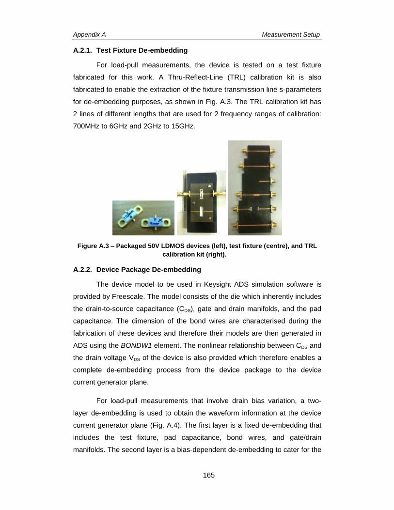
Appendix A Measurement Setup
165
A.2.1. Test Fixture De-embedding
For load-pull measurements, the device is tested on a test fixture
fabricated for this work. A Thru-Reflect-Line (TRL) calibration kit is also
fabricated to enable the extraction of the fixture transmission line s-parameters
for de-embedding purposes, as shown in Fig. A.3. The TRL calibration kit has
2 lines of different lengths that are used for 2 frequency ranges of calibration:
700MHz to 6GHz and 2GHz to 15GHz.
Figure A.3 – Packaged 50V LDMOS devices (left), test fixture (centre), and TRL
calibration kit (right).
A.2.2. Device Package De-embedding
The device model to be used in Keysight ADS simulation software is
provided by Freescale. The model consists of the die which inherently includes
the drain-to-source capacitance (CDS), gate and drain manifolds, and the pad
capacitance. The dimension of the bond wires are characterised during the
fabrication of these devices and therefore their models are then generated in
ADS using the BONDW1 element. The nonlinear relationship between CDS and
the drain voltage VDS of the device is also provided which therefore enables a
complete de-embedding process from the device package to the device
current generator plane.
For load-pull measurements that involve drain bias variation, a two-
layer de-embedding is used to obtain the waveform information at the device
current generator plane (Fig. A.4). The first layer is a fixed de-embedding that
includes the test fixture, pad capacitance, bond wires, and gate/drain
manifolds. The second layer is a bias-dependent de-embedding to cater for the
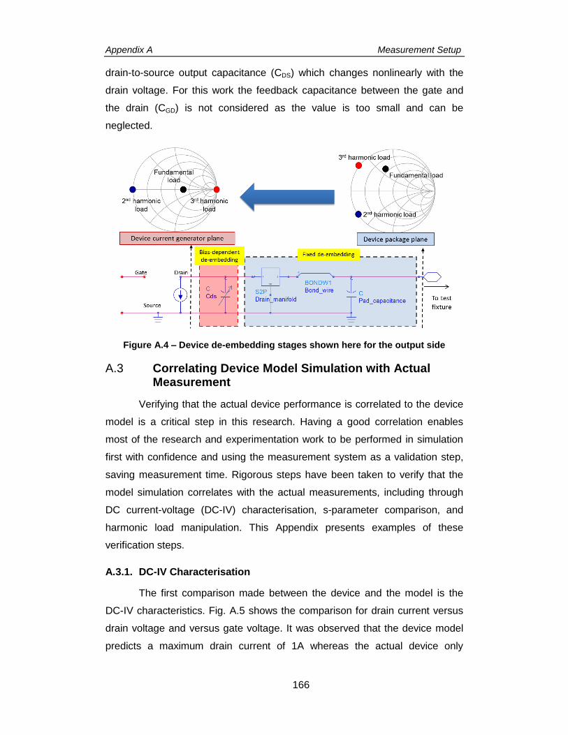
Appendix A Measurement Setup
166
drain-to-source output capacitance (CDS) which changes nonlinearly with the
drain voltage. For this work the feedback capacitance between the gate and
the drain (CGD) is not considered as the value is too small and can be
neglected.
Figure A.4 – Device de-embedding stages shown here for the output side
Correlating Device Model Simulation with Actual A.3 Measurement
Verifying that the actual device performance is correlated to the device
model is a critical step in this research. Having a good correlation enables
most of the research and experimentation work to be performed in simulation
first with confidence and using the measurement system as a validation step,
saving measurement time. Rigorous steps have been taken to verify that the
model simulation correlates with the actual measurements, including through
DC current-voltage (DC-IV) characterisation, s-parameter comparison, and
harmonic load manipulation. This Appendix presents examples of these
verification steps.
A.3.1. DC-IV Characterisation
The first comparison made between the device and the model is the
DC-IV characteristics. Fig. A.5 shows the comparison for drain current versus
drain voltage and versus gate voltage. It was observed that the device model
predicts a maximum drain current of 1A whereas the actual device only
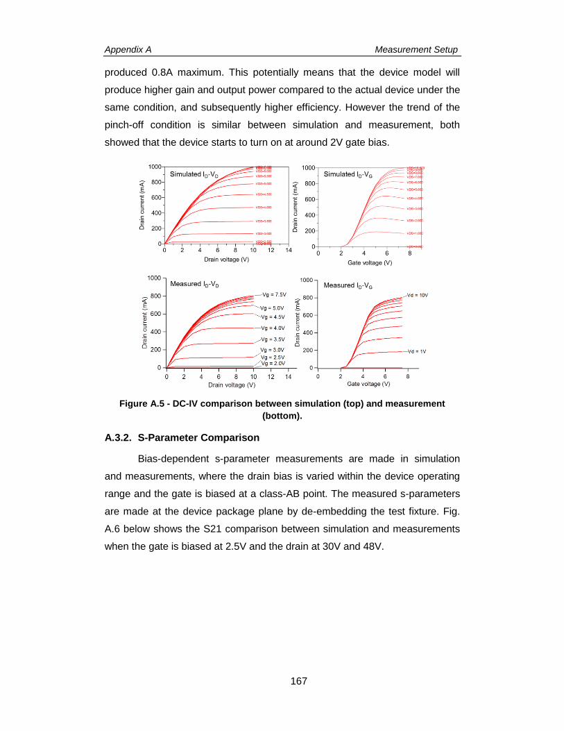
Appendix A Measurement Setup
167
produced 0.8A maximum. This potentially means that the device model will
produce higher gain and output power compared to the actual device under the
same condition, and subsequently higher efficiency. However the trend of the
pinch-off condition is similar between simulation and measurement, both
showed that the device starts to turn on at around 2V gate bias.
Figure A.5 - DC-IV comparison between simulation (top) and measurement
(bottom).
A.3.2. S-Parameter Comparison
Bias-dependent s-parameter measurements are made in simulation
and measurements, where the drain bias is varied within the device operating
range and the gate is biased at a class-AB point. The measured s-parameters
are made at the device package plane by de-embedding the test fixture. Fig.
A.6 below shows the S21 comparison between simulation and measurements
when the gate is biased at 2.5V and the drain at 30V and 48V.
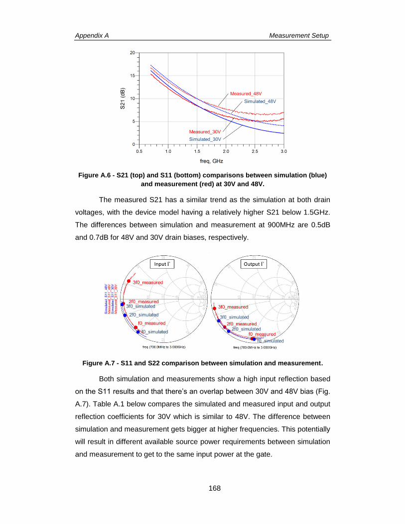
Appendix A Measurement Setup
168
Figure A.6 - S21 (top) and S11 (bottom) comparisons between simulation (blue)
and measurement (red) at 30V and 48V.
The measured S21 has a similar trend as the simulation at both drain
voltages, with the device model having a relatively higher S21 below 1.5GHz.
The differences between simulation and measurement at 900MHz are 0.5dB
and 0.7dB for 48V and 30V drain biases, respectively.
Figure A.7 - S11 and S22 comparison between simulation and measurement.
Both simulation and measurements show a high input reflection based
on the S11 results and that there’s an overlap between 30V and 48V bias (Fig.
A.7). Table A.1 below compares the simulated and measured input and output
reflection coefficients for 30V which is similar to 48V. The difference between
simulation and measurement gets bigger at higher frequencies. This potentially
will result in different available source power requirements between simulation
and measurement to get to the same input power at the gate.

Appendix A Measurement Setup
169
Frequency Simulated
ΓIN
Measured
ΓIN
Simulated
ΓOUT
Measured
ΓOUT
900MHz 0.96 -128 0.92 -135 0.91 -91 0.91 -94
1.8GHz 0.97 -157 0.94 -174 0.95 -129 0.94 -137
2.7GHz 0.97 -173 0.91 153 0.96 -149 0.95 -167
Table A.1 – Input reflection comparison between simulation and measurement.
A.3.3. Harmonic Load Manipulation Comparison
Ultimately the correlation of interest between simulation and
measurement is in the performance at the current generator plane under a
certain harmonic load combination, an exercise that takes into account the
effect of de-embedding accuracy. This section presents the steps taken in
determining the right CDS de-embedding for load-pull, followed by the
simulation and measurement comparison of a class-F mode PA.
The first step is to find the right de-embedding for the actual device.
Using load-pull measurements, a search for maximum efficiency point is
performed and different CDS values are iteratively used until the maximum
output power and efficiency of the load-pull contours are located on the real
axis of the Smith chart. Fig. A.8 shows the iteration performed for the 48V drain
bias setting, where the optimum CDS value for de-embedding was found to be
1.3pF. This step is repeated at other drain bias settings as well.
Figure A.8 - Iterations to find the right de-embedding in measurements.
The next step is to compare simulated load-pull against measured load-
pull, with the same harmonic load combination on the current generator plane.
The comparison shown in this section is achieved by performing a power
sweep at 28V drain bias with the PA set to operate in a class-F mode. The
fundamental load presented to the current generator plane in this example is

Appendix A Measurement Setup
170
117Ω which is targeting a maximum efficiency performance, while the 2nd and
3rd harmonics are presented with a short and an open circuit, respectively. Fig.
A.9 compares the gain and PAE between the model and actual device as a
function of output back-off from peak power. The model has approximately
0.8dB higher gain before the compression region, as predicted from the DC-IV
differences. This produces a PAE of close to 80% at its peak, while the
measured device exhibits a maximum PAE of 74%. The maximum output
power from simulation in this case is 36.4dBm, 0.6dB higher than the
measured output. Although the absolute performance result values are
different, the actual device does exhibit the same trend as the model.
Figure A.9 – Gain and PAE comparison between simulation and measurement.
Fig. A.10 shows the DC, fundamental, and 2nd harmonic current at the
drain as a function of the input voltage magnitude, normalized to the location of
maximum gain. Both simulation and measurement show a similar trend,
although the model generates higher fundamental drain current output.
Finally the simulated and measured time-domain waveforms with power
sweep of up to 5dB compression are compared, as shown in Fig. A.11. The
squared voltage waveform characteristic of class-F can be seen on both cases,
with the simulation having a slightly bigger swing. The measured current peaks
at 650mA compared to 600mA from simulation. This small difference could be
attributed to the difference in the fundamental impedance presented to the
current generator plane or residual de-embedding error between simulation
and load-pull. However in general the device model does show a good
20
18
16
14
Gain
(dB
)
-6 -4 -2 0
Output back-off from peak power (dB)
80
70
60
50
40
PA
E (%
)
Simulated gain Simulated PAE Measured gain Measured PAE
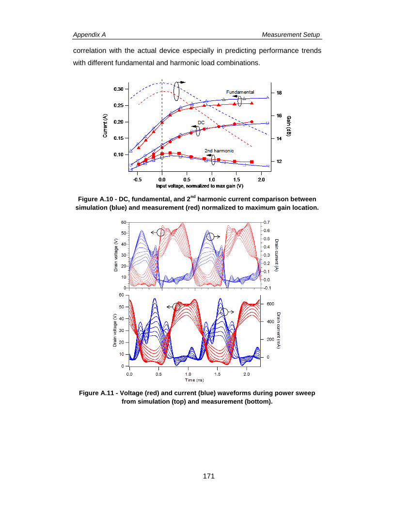
Appendix A Measurement Setup
171
correlation with the actual device especially in predicting performance trends
with different fundamental and harmonic load combinations.
Figure A.10 - DC, fundamental, and 2nd
harmonic current comparison between
simulation (blue) and measurement (red) normalized to maximum gain location.
Figure A.11 - Voltage (red) and current (blue) waveforms during power sweep
from simulation (top) and measurement (bottom).
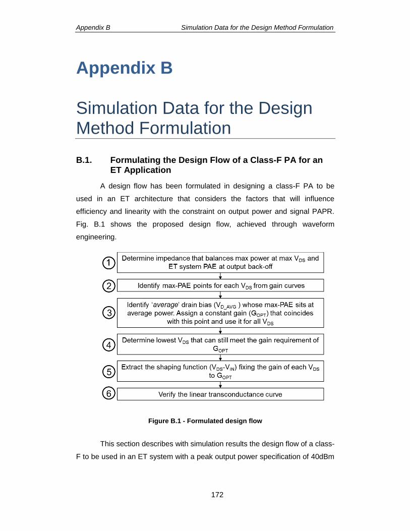
Appendix B Simulation Data for the Design Method Formulation
172
Appendix B Simulation Data for the Design Method Formulation
B.1. Formulating the Design Flow of a Class-F PA for an ET Application
A design flow has been formulated in designing a class-F PA to be
used in an ET architecture that considers the factors that will influence
efficiency and linearity with the constraint on output power and signal PAPR.
Fig. B.1 shows the proposed design flow, achieved through waveform
engineering.
Figure B.1 - Formulated design flow
This section describes with simulation results the design flow of a class-
F to be used in an ET system with a peak output power specification of 40dBm
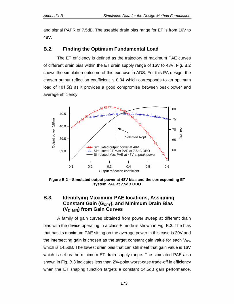
Appendix B Simulation Data for the Design Method Formulation
173
and signal PAPR of 7.5dB. The useable drain bias range for ET is from 16V to
48V.
B.2. Finding the Optimum Fundamental Load
The ET efficiency is defined as the trajectory of maximum PAE curves
of different drain bias within the ET drain supply range of 16V to 48V. Fig. B.2
shows the simulation outcome of this exercise in ADS. For this PA design, the
chosen output reflection coefficient is 0.34 which corresponds to an optimum
load of 101.5Ω as it provides a good compromise between peak power and
average efficiency.
Figure B.2 – Simulated output power at 48V bias and the corresponding ET system PAE at 7.5dB OBO
B.3. Identifying Maximum-PAE locations, Assigning Constant Gain (GOPT), and Minimum Drain Bias (VD_MIN) from Gain Curves
A family of gain curves obtained from power sweep at different drain
bias with the device operating in a class-F mode is shown in Fig. B.3. The bias
that has its maximum PAE sitting on the average power in this case is 20V and
the intersecting gain is chosen as the target constant gain value for each VDS,
which is 14.5dB. The lowest drain bias that can still meet that gain value is 16V
which is set as the minimum ET drain supply range. The simulated PAE also
shown in Fig. B.3 indicates less than 2%-point worst-case trade-off in efficiency
when the ET shaping function targets a constant 14.5dB gain performance,
40.5
40.0
39.5
39.0
Outp
ut pow
er
(dB
m)
0.60.50.40.30.20.1
Output reflection coefficient
80
75
70
65
60
PA
E (%
)
Simulated output power at 48V Simulated ET Max PAE at 7.5dB OBO Simulated Max PAE at 48V at peak power
Selected Ropt
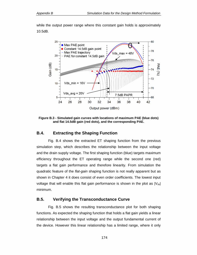
Appendix B Simulation Data for the Design Method Formulation
174
while the output power range where this constant gain holds is approximately
10.5dB.
Figure B.3 - Simulated gain curves with locations of maximum PAE (blue dots) and flat 14.5dB gain (red dots), and the corresponding PAE.
B.4. Extracting the Shaping Function
Fig. B.4 shows the extracted ET shaping function from the previous
simulation step, which describes the relationship between the input voltage
and the drain supply voltage. The first shaping function (blue) targets maximum
efficiency throughout the ET operating range while the second one (red)
targets a flat gain performance and therefore linearity. From simulation the
quadratic feature of the flat-gain shaping function is not really apparent but as
shown in Chapter 4 it does consist of even order coefficients. The lowest input
voltage that will enable this flat gain performance is shown in the plot as |VIN|
minimum.
B.5. Verifying the Transconductance Curve
Fig. B.5 shows the resulting transconductance plot for both shaping
functions. As expected the shaping function that holds a flat gain yields a linear
relationship between the input voltage and the output fundamental current of
the device. However this linear relationship has a limited range, where it only
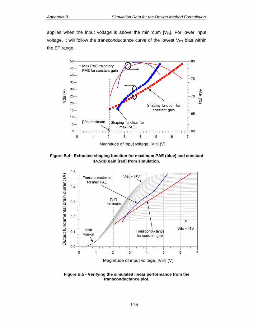
Appendix B Simulation Data for the Design Method Formulation
175
applies when the input voltage is above the minimum |VIN|. For lower input
voltage, it will follow the transconductance curve of the lowest VDS bias within
the ET range.
Figure B.4 - Extracted shaping function for maximum PAE (blue) and constant
14.5dB gain (red) from simulation.
Figure B.5 - Verifying the simulated linear performance from the transconductance plot.

Appendix C Continuous Mode Power Amplifier Theory
176
Appendix C Continuous Mode Power Amplifier Theory
C.1. Introduction
The basis of the continuous mode power amplifier starts with the
formulation of the class-J power amplifier that was introduced by Cripps in [1].
The class-J applies a phase shift on the fundamental and 2nd harmonic loads of
a class-B mode PA at -45° and 90°, respectively and retains the class-B output
power and efficiency performance. The work in [2] further presented a design
space continuum between the class-B and class-J states which would maintain
the same output power and efficiency performance, enabling a high bandwidth
design of matching network. This continuous mode of operation is referred to
as the continuous class-BJ mode.
C.2. Formulation of the Continuous Class-BJ Mode
The continuous class-BJ mode of operation has a half-rectified current
waveform as class-B but applies a raised sine function of the continuous mode
operator (1 − 𝛼 sin 𝜗) to the normalized class-B output voltage:
𝐼𝐶𝑜𝑛𝑡𝐵𝐽(𝜗) = 𝐼𝑚𝑎𝑥 cos 𝜗 0 < 𝜗 <
𝜋
2 and
3𝜋
2< 𝜗 < 2𝜋
= 0 𝜋
2< 𝜗 <
3𝜋
2
(C.1)
𝑉𝐶𝑜𝑛𝑡_𝐵𝐽 = 𝑉𝑚𝑎𝑥(1 − cos 𝜗) ∙ (1 − 𝛼 sin 𝜗) (C.2)
where the range of α is defined from -1 to 1 in order to keep the voltage
above zero. Multiplying out the terms in (C.2) yields:

Appendix C Continuous Mode Power Amplifier Theory
177
𝑉𝐶𝑜𝑛𝑡_𝐵𝐽 = 𝑉𝑚𝑎𝑥(1 − cos 𝜗 − 𝛼 sin 𝜗 +𝛼
2sin 2𝜗) (C.3)
Fig. C.1 shows the ideal normalized output voltage and current
waveforms of a class-BJ mode power amplifier as the variable α is varied from
-1 to 1 in 0.2 steps. At α=0 (shown in black) the voltage waveform returns to a
class-B output state. It is noted that the voltage swing of the class-BJ mode
increases by almost a factor of 1.5 from the class-B state at α=-1 and α=1.
Figure C.1 – Output voltage (red, black) and current (blue) waveforms of class-BJ power amplifier when α is varied from -1 to 1 in 0.2 steps.
The normalized DC, fundamental and 2nd harmonic frequency voltage
components can be extracted from C.3:
𝑉𝐷𝐶 = 1 (C.4)
𝑉𝑓0(𝛼) = −1 + 𝑗𝛼 (C.5)
𝑉2𝑓0(𝛼) = 0 − 𝑗𝛼
2 (C.6)
From the voltage and current equations the fundamental and second
harmonic loads can be derived as a function of α:
𝑍𝑓0 = 𝑅𝑜𝑝𝑡 − 𝑗 ∙ 𝛼 ∙ 𝑅𝑜𝑝𝑡 (C.7)
𝑍2𝑓0 = − 𝑗 ∙ 𝛼 ∙3𝜋
8∙ 𝑅𝑜𝑝𝑡 (C.8)
where ROPT is the normalized optimum load. Again, at α=0 the pair of
load impedances return to the class-B load state. It is noted from (C.8) that the

Appendix C Continuous Mode Power Amplifier Theory
178
2nd harmonic load is always located on the edge of the Smith chart. Fig. C.2
shows the trajectories of the fundamental and 2nd harmonic loads on the Smith
chart as α is varied from -1 to 1 with ROPT=101.5Ω from Chapter 5.
Figure C.2 – Trajectories of fundamental (blue) and 2nd harmonic loads (red) of a class-BJ power amplifier with ROPT=101.5Ω for -1<α<1 in 0.2 steps.
The resulting normalized output power and theoretical efficiency is
maintained at 1 and 78.5%, respectively throughout α values from -1 to 1 as
shown in Fig. C.3.
C.3. Formulation of the Continuous Class-F Mode
The continuous mode operator of (1 − 𝛼 sin 𝜗) can also be applied to
the output voltage of class-F to produce the continuous class-F mode. Class-F
mode has the same half-rectified current waveform as class-B while the output
voltage is ideally a squared waveform if infinite harmonics are used. For this
analysis only the first 3 harmonics are considered as described in [3] and
applying the raised sine function of the continuous mode operator produces
the voltage equations below:
𝑉𝐶𝑜𝑛𝑡_𝐹 = 𝑉𝑚𝑎𝑥 (1 −2
√3cos 𝜗 +
1
3√3cos 3𝜗) ∙ (1 − 𝛼 sin 𝜗)
(C.9)
which can be expanded into the equation below, showing up to the 3rd
harmonic component:
𝑉𝐶𝑜𝑛𝑡_𝐹 = 𝑉𝑚𝑎𝑥(1 −2
√3cos 𝜗 − 𝛼 sin 𝜗 +
7
6√3𝛼 sin 2𝜗 +
1
3√3cos 3𝜗) (C.10)
2.0
1.5
1.0
0.5
0.0
-0.5
-1.0
-1.0 -0.5 0.0 0.5 1.0
= -1
= 1
= 1
= -1
= 0
Fundamental 2nd harmonic

Appendix C Continuous Mode Power Amplifier Theory
179
The normalized individual frequency components can therefore be
extracted:
𝑉𝐷𝐶 = 1 (C.11)
𝑉𝑓0(𝛼) = −2
√3+ 𝑗 ∙ 𝛼 (C.12)
𝑉2𝑓0(𝛼) = −𝑗7
6√3∙ 𝛼 (C.13)
𝑉3𝑓0(𝛼) =1
3√3 (C.14)
It is noted that only the fundamental and 2nd harmonic voltages have a
dependency on α. Fig. C.3 shows the ideal normalized output voltage and
current waveforms of a continuous class-F with α varied from -1 to 1 in 0.2
steps, as well as the theoretical efficiency performance and normalized output
power. As with the previous section, at α=0 the output waveforms become the
conventional class-F waveforms.
Figure C.3 – Top: Output voltage (red, black) and current (blue) waveforms of a continuous class-F power amplifier when α is varied from -1 to 1 in 0.2 steps.
Bottom: Efficiency and normalized output power for continuous class-BJ and F.

Appendix C Continuous Mode Power Amplifier Theory
180
Dividing each component with the corresponding current component
results in the following load impedances for the fundamental, 2nd, and 3rd
harmonic components:
𝑍𝑓0 = 𝑅𝑜𝑝𝑡 − 𝑗√3
2𝛼 ∙ 𝑅𝑜𝑝𝑡 (C.15)
𝑍2𝑓0(𝛼) = 𝑗 ∙ 1.375 ∙ 𝛼 (C.16)
𝑍3𝑓0(𝛼) = ∞ (𝑜𝑝𝑒𝑛 𝑐𝑖𝑟𝑐𝑢𝑖𝑡) (C.17)
Fig. C.4 shows the trajectory of the continuous class-F mode with α
varied from -1 to 1 using the same ROPT of 101.5Ω from the previous chapter.
The 3rd harmonic load remains in an open circuit condition while the
trajectories of fundamental and 2nd harmonic loads move in opposite directions.
Figure C.4 – Trajectories of fundamental, 2nd
, and 3rd harmonic loads of a continuous class-F power amplifiers with ROPT=101.5Ω for -1<α<1 in 0.2 steps.
C.4. References
[1] S. C. Cripps, RF Power Amplifiers for Wireless Communications: Artech House, 2006.
[2] S. C. Cripps, P. J. Tasker, A. L. Clarke, J. Lees, and J. Benedikt, "On the Continuity of High Efficiency Modes in Linear RF Power Amplifiers," Microwave and Wireless Components Letters, IEEE, vol. 19, pp. 665-667, 2009.
[3] P. Colantonio, F. Giannini, G. Leuzzi, and E. Limiti, "On the class-F power amplifier design," International Journal of Rf and Microwave Computer-Aided Engineering, vol. 9, pp. 129-149, Mar 1999.
2.0
1.5
1.0
0.5
0.0
-0.5
-1.0
-1.0 -0.5 0.0 0.5 1.0
= -1
= 1
= 1
= -1
= 0
Fundamental 2nd harmonic 3rd harmonic

Appendix D Voltage-Pull Simulation Method
181
Appendix D Voltage-Pull Simulation Method
D.1. Setting up the Voltage-Pull Simulation
The voltage-pull simulation is performed in ADS using the Harmonic
Balance simulator. Fig D.1 shows the ADS schematic where a V_nHarm
voltage source is connected to the load side of the device. The device model is
a die model with intrinsic drain-source capacitance (CDS). To probe the voltage
and current waveforms at the current generator plane (IGEN), a negative
capacitor is used for de-embedding. This negative CDS value is fixed based on
the value given by the manufacturer based on the drain bias voltage.
In this simulation the waveforms after the CDS which contains the sum
of the displacement current and IGEN is obtained by placing back a positive CDS.
Another negative CDS is required to enable probing at the IGEN plane.
The continuous class-BJ voltage equations as a function of α as
described in Appendix C are used to define the DC, fundamental, and 2nd
harmonic voltage magnitudes respectively, while higher harmonic voltages are
set to zero. The phases of these components are initially set to zero but in the
later part of the simulation their values will change to simulate the effect of
phase-shifting.
The desired impedance at α=0 is achieved by adjusting the magnitude
of the voltage source at fundamental frequency. The parameter α is swept from
-1 to 1 in 0.2 steps, modifying the output voltage and the output power and
PAE are recorded.

Appendix D Voltage-Pull Simulation Method
182
Figure D.1 – Voltage pull simulation setup with a fixed CDS de-embedding (top),
and the equations used in the analysis (bottom).
To simulate a phase shift effect on the output voltage and bring the 2nd
harmonic loads to the edge of the Smith chart, the phase of the V_nHarm
source is changed manually using the ADS Tuning function.

Appendix E Calculating the Lossy Varactor
183
Appendix E Calculating the Lossy Varactor
E.1. Calculating the Current and Voltage: an Iterative Approach
To model a lossy varactor, a series resistor is added in series with CDS
as shown in Fig. E.1. The Igor program developed in Section 6.5 is modified to
iteratively calculate the varactor voltage and current for a given series resistor
value as shown in Fig. E.2. At the start of the iteration the ‘lossless’ varactor
voltage is used to determine the corresponding CDS and varactor current. With
a known series resistor value assigned, the calculated current is then used to
calculate the next iteration of varactor voltage VNEXT using Kirchhoff’s Voltage
Law. This voltage is then compared with the previous iteration and an error
voltage is calculated. The magnitude of the error voltage is used to determine if
the next iteration is required. The process is repeated until the error is reduced
to near zero or until the iteration reaches a certain limit. A weighting factor is
applied in the voltage iteration to improve convergence success rate.
Figure E.1 – Modified circuit diagram to represent a lossy varactor.
E.2. Estimating the Varactor Series Resistance of the Actual Device
In order to estimate the series resistance of the device used in Section
7.5, the varactor and device parameters are modified to reflect its actual
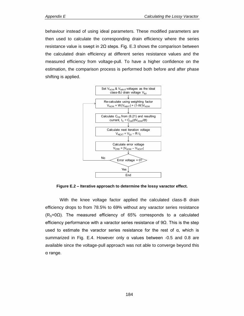
Appendix E Calculating the Lossy Varactor
184
behaviour instead of using ideal parameters. These modified parameters are
then used to calculate the corresponding drain efficiency where the series
resistance value is swept in 2Ω steps. Fig. E.3 shows the comparison between
the calculated drain efficiency at different series resistance values and the
measured efficiency from voltage-pull. To have a higher confidence on the
estimation, the comparison process is performed both before and after phase
shifting is applied.
Figure E.2 – Iterative approach to determine the lossy varactor effect.
With the knee voltage factor applied the calculated class-B drain
efficiency drops to from 78.5% to 69% without any varactor series resistance
(RS=0Ω). The measured efficiency of 65% corresponds to a calculated
efficiency performance with a varactor series resistance of 9Ω. This is the step
used to estimate the varactor series resistance for the rest of α, which is
summarized in Fig. E.4. However only α values between -0.5 and 0.8 are
available since the voltage-pull approach was not able to converge beyond this
α range.
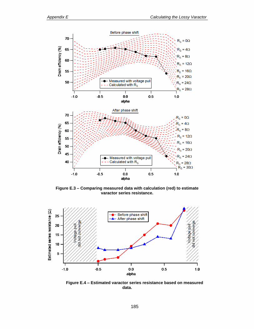
Appendix E Calculating the Lossy Varactor
185
Figure E.3 – Comparing measured data with calculation (red) to estimate varactor series resistance.
Figure E.4 – Estimated varactor series resistance based on measured data.