Embed Size (px)
Citation preview
http://wjst.wu.ac.th Engineering and Physical Sciences
Walailak J Sci & Tech 2017; 14(4): 339-351.
Design of A New High-Gain Multiband and Wideband Rectangular Patch Antenna for C, X, and Ku Band Applications Soufian LAKRIT1,*, Hassan AMMOR1, Jaouad TERHZAZ2 and Abdelwahd TRIBAK3
1Electronic and Communication Laboratory, EMI, Mohammed V University of Rabat, Morocco 2Centre Régional des Métiers de l’éducation et de la Formation (CRMEF), Casablanca, Morocco 3Institut National de Poste et Telecommunications (INPT), Rabat, Morocco (*Corresponding author’s e-mail: [email protected]) Received: 3 September 2015, Revised: 1 May 2016, Accepted: 9 June 2016 Abstract
In this paper, we propose the design of and provide an analysis of, a rectangular patch antenna and its integration in a 4 element linear array. A T form power divider feeds in parallel the array elements through microstrip lines. The basic antenna has a simple structure, with dimensions of about 16×18×1.6 mm3, leading to a good bandwidth. In addition, the patch element characteristics, such as the reflection coefficient and the voltage standing wave ratio (VSWR), are improved by the insertion of a slot in the structure. The main objective of the 4 element array structure is the enhancement of the gain, which is enhanced up to 12.6 dBi. A prototype of the antenna is fabricated and tested with network analyzer. The proposed antenna has 4 resonant frequencies that define 4 bandwidths, defined by a return loss of less than −10 dB, and are: (7.62 GHz, 1250 MHz), (9.20 GHz, 330 MHz), (11.07 GHz, 940 MHz) and (15.02 GHz, 920 MHz), respectively. The simple configuration of this profile permits an easy and low-expense fabrication process, with usability in many applications such as in radar, satellite, and wireless communications.
Keywords: Microstrip antenna, linear array, high-gain, wideband, X-band, radar, satellite Introduction
The rapid development of modern wireless technologies has stimulated growth in research in the field of microstrip antennas. These radiating elements are miniature and lightweight, and gathering them in arrays leads to high gains. This makes equipment made of this type of antenna reliable, mobile, and with efficient radiation characteristics [1]. In addition, they can be manufactured using printed circuit technology with moderate cost and easiness, giving them conformability with complex mounting surfaces [2]. Thus, this type of radiating element has become increasingly popular in many wireless systems, such as satellite communications, radar, medical applications, etc [3]. However, a main disadvantage of the patch antenna radiator is its narrow bandwidth. Recently, many techniques have been developed to enhance this bandwidth. The most commonly used ones add slots to the radiating element [4-7] and include a partial ground plane [8,9]. In addition, the microstrip antennas have low gains, and do not tolerate high power levels. Therefore, the challenge in microstrip antenna design is to increase both bandwidth and gain [10]. Patch antenna arrays have been widely reported in the literature [11-14], and several authors [14-16] have focused on the technical design of microstrip patch antennas for X-band applications.
In this paper, a new high-gain wideband microstrip patch antenna, operating in 3 bands C, X, and Ku, is presented. This structure has several advantages, such as its smallness and the simplicity of its

Design of A New High-Gain Multiband and Wideband Rectangular Patch Antenna Soufian LAKRIT et al. http://wjst.wu.ac.th
Walailak J Sci & Tech 2017; 14(4) 340
structure, which leads to an easy manufacturing process. Feeding is ensured by a microstrip line with 50 Ω. The antenna design was performed using the Ansoft High Frequency Structure Simulator (HFSS).
When compared with other printed radiating elements, our antenna possesses the advantage of not only having a broad bandwidth, but also a smaller size [7,14,16,17]. Rectangular microstrip antenna theory
In order to understand the design and analysis processes of our microstrip antenna shown in Figure 1, there are some important principles and theoretical tools [18] that should be presented.
Patch length & width
Figure 1 Geometry of the patch antenna.
Choosing a rectangular shape for our antenna allows us to think of how to relate the dimensions, W and L, to the radiation characteristics of this radiating element. The width, W, influences the radiated power and the bandwidth. Thus, W is chosen so that the bandwidth and the radiation efficiency are satisfactory. The literature suggests that 1 < W/L < 2 [19]. Further, the length, L, influences the resonant frequency to which it is linked by (1) [20];
𝐿 = 𝐶
2𝑓𝑟√𝜀𝑟 (1)
where fr is the resonant frequency.
Fringing effect The fringing effect is accounted for by defining an effective dielectric constant, εreff, as follows [20];
𝜀𝑟𝑒𝑓𝑓 = 𝜀𝑟+12
+ 𝜀𝑟−121 + 12 ℎ
𝑊12 , 𝑊
ℎ≫ 1 (2)
𝜀𝑟𝑒𝑓𝑓 = 𝜀𝑟+12
+ 𝜀𝑟−121 + 12 ℎ
𝑊12 + 0.041 1 − 𝑊
ℎ , 𝑊
ℎ≪ 1 (3)
Length and width and fringing effect The fringing effect influences the calculation of L and W as follows [20];
W
h L
x
y z Ground
plane
Feeding point
Design of A New High-Gain Multiband and Wideband Rectangular Patch Antenna Soufian LAKRIT et al. http://wjst.wu.ac.th
Walailak J Sci & Tech 2017; 14(4)
341
𝑊 = 𝐶
2𝑓𝑟 𝜀𝑟+12
(4)
As for the length L, we define an effective length by using εreff in (1) and subtracting 2ΔL [20];
𝐿 = 𝐶2𝑓𝑟𝜀𝑟𝑒𝑓𝑓
− 2∆𝐿 (5)
ΔL is called the normalized length extension, and is given by [20];
∆𝐿 = 0.412ℎ(𝜀𝑟+0.3)𝑊ℎ+0.364
(𝜀𝑟+0.258)𝑊ℎ+0.8 (6)
Theory of linear array
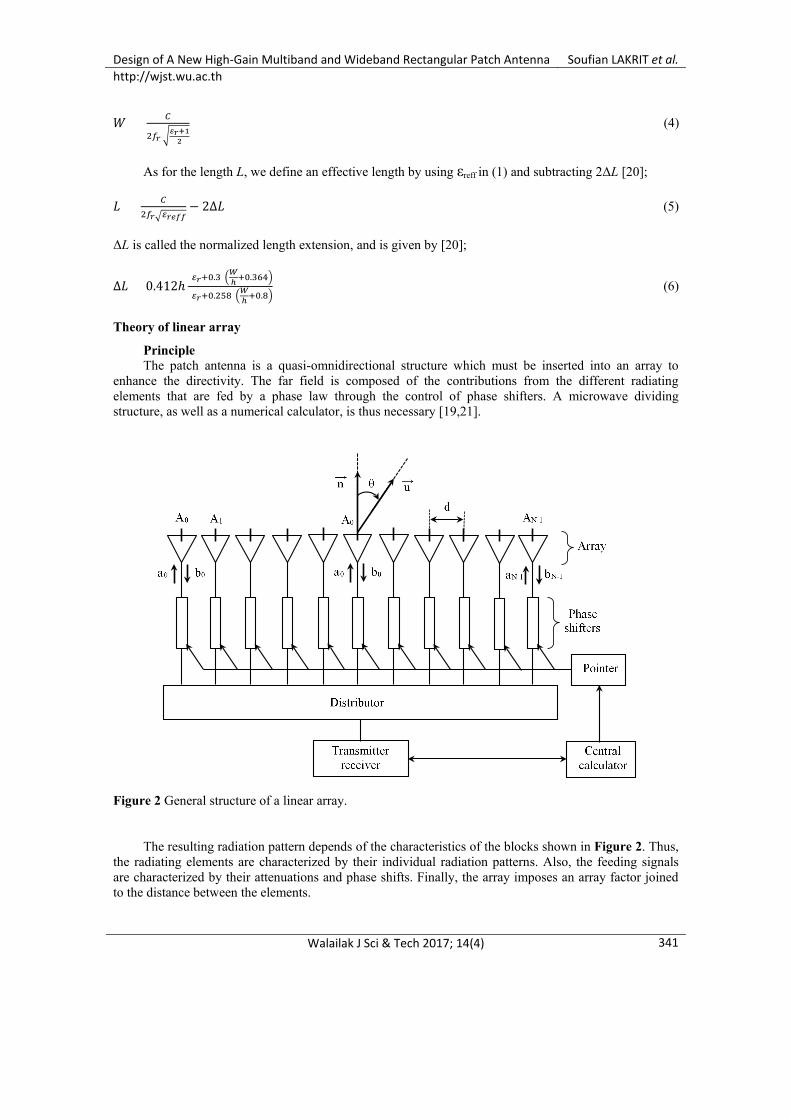
Principle The patch antenna is a quasi-omnidirectional structure which must be inserted into an array to
enhance the directivity. The far field is composed of the contributions from the different radiating elements that are fed by a phase law through the control of phase shifters. A microwave dividing structure, as well as a numerical calculator, is thus necessary [19,21].
Figure 2 General structure of a linear array.
The resulting radiation pattern depends of the characteristics of the blocks shown in Figure 2. Thus, the radiating elements are characterized by their individual radiation patterns. Also, the feeding signals are characterized by their attenuations and phase shifts. Finally, the array imposes an array factor joined to the distance between the elements.

Design of A New High-Gain Multiband and Wideband Rectangular Patch Antenna Soufian LAKRIT et al. http://wjst.wu.ac.th
Walailak J Sci & Tech 2017; 14(4) 342
The phase control influences the directivity of the resulting pattern, and the amplitude control influences the side-lobes level. Also, a high number of elements results in a fine pattern. The derivation of these laws is based on the theory of interferences, which must be constructive in the main lobe and destructive in the side lobes [22]. Figure 3 gives the different possible configurations of arrays.
There are 2 main ways to feed the different elements of the array, presented in Figure 4. On the one hand, the series feeding relies on the length of the line joining to 2 consecutive elements. On the other hand, parallel feeding relies on using a power divider with phase shifters.
(a) (b) (c) Figure 3 Different geometric configurations of the arrays, linear (a), 2-dimensional (b), and circular (c).
Figure 4 Feeding of a one-dimensional array.
In order to make a choice between series and parallel feeding, we base the decision on the desired performances. So, the weighting law is tightly related to the configuration. Thus, in a series configuration, the phase shifting depends on the line length and the frequency, and do not permit a broad band. Also, the functional weighting role of the lines connecting a series configuration contributes to a reduction in the array size.
Array antenna design considerations To design an array, we must choose its geometry (linear, rectangular, circular, etc.). This is imposed
by the platform on which it will be installed. Next, we have to specify the distance separating the elements, which must not be too high, in order to avoid mutual coupling, and must not be too low, in order to avoid side-lobes. The literature [21] shows that the distance that gives the optimal gain is between 0.25 and 2 λ. Also, computer control of the amplitude and phase are necessary to shape the pattern. Finally, the individual pattern of each radiating element contributes heavily to the global pattern, whose gain is theoretically doubled when we double the number of elements.
Series
Parallel

Design of A New High-Gain Multiband and Wideband Rectangular Patch Antenna Soufian LAKRIT et al. http://wjst.wu.ac.th
Walailak J Sci & Tech 2017; 14(4)
343
One-dimensional array Figure 5 schematizes the situation when we gather N radiating elements, separated by the distance
d on the [O, X) axis.
Figure 5 One-dimensional array.
In order to calculate the field produced by this distribution at a far point M, we assume for simplification that there is no coupling between the elements, and that all the elements have the same radiation pattern, F(θ).
The resulting field is the sum of the contribution by the elements, weighted by their attenuations and phase shifting, as shown in (5). 𝑓(𝜃) = 𝐹(𝜃)∑ 𝑤𝑖𝑒𝑗(𝑘0𝑖𝑑 sin𝜃) 𝑁−1
𝑖=0 (7) Or, more compactly; 𝑓(𝜃) = 𝐹(𝜃)𝐹𝑅(𝜃) (8) where I is the radiating element index. N is the number of array elements. 𝐹(𝜃) is the pattern of an individual element. 𝑘0 = 2𝜋
𝜆 is the propagation constant.
FR is the array factor that depends on the array shape and the feeding law represented by the
weightings, wi. It summarizes physically the enhancement of gain provided by the array [23]. Design procedure
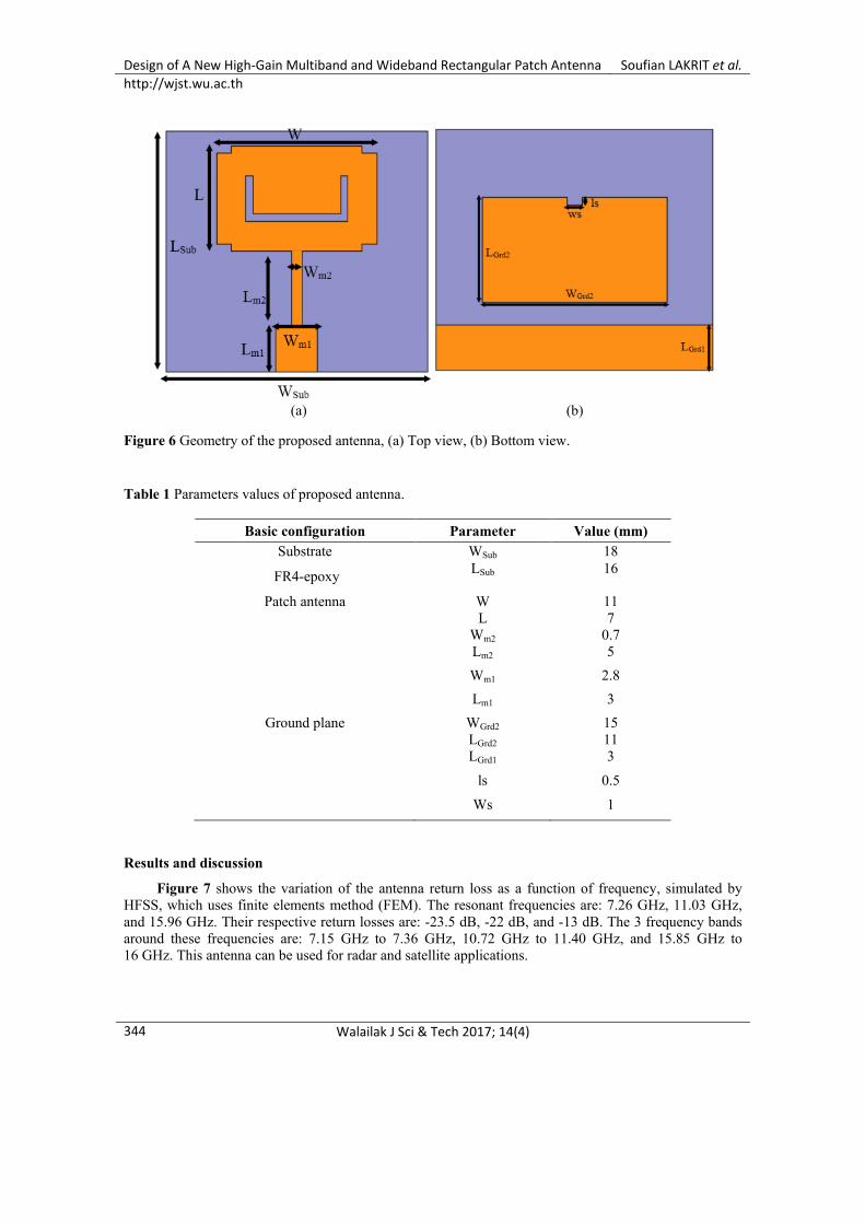
Antenna element design In this paper, we present a microstrip patch antenna, shown in Figure 6. It has a rectangular form, to
which we have added some shapes: steps, slots, and a U-shaped slot. On the other side, we have made a partial ground plane, beside which we added a parasitic element, in which there is a slot to broaden the bandwidth. The substrate is FR4-epoxy, with dimensions of 18×20×1.6 mm3. It is characterized by a thickness of 1.6 mm, a dielectric permittivity of 4.4, and a loss tangent of 0.02. The feeding is ensured by a microstrip line matched to 50 Ω by a quarter wavelength line. The design and optimization was done by HFSS, and has led to the parameters summarized in Table 1.
Design of A New High-Gain Multiband and Wideband Rectangular Patch Antenna Soufian LAKRIT et al. http://wjst.wu.ac.th
Walailak J Sci & Tech 2017; 14(4) 344
(a) (b) Figure 6 Geometry of the proposed antenna, (a) Top view, (b) Bottom view. Table 1 Parameters values of proposed antenna.
Basic configuration Parameter Value (mm) Substrate
FR4-epoxy
WSub 18 LSub 16
Patch antenna W 11 L 7
Wm2 0.7 Lm2 5
Wm1 2.8 Lm1 3
Ground plane WGrd2 15 LGrd2 11 LGrd1 3
ls 0.5
Ws 1
Results and discussion
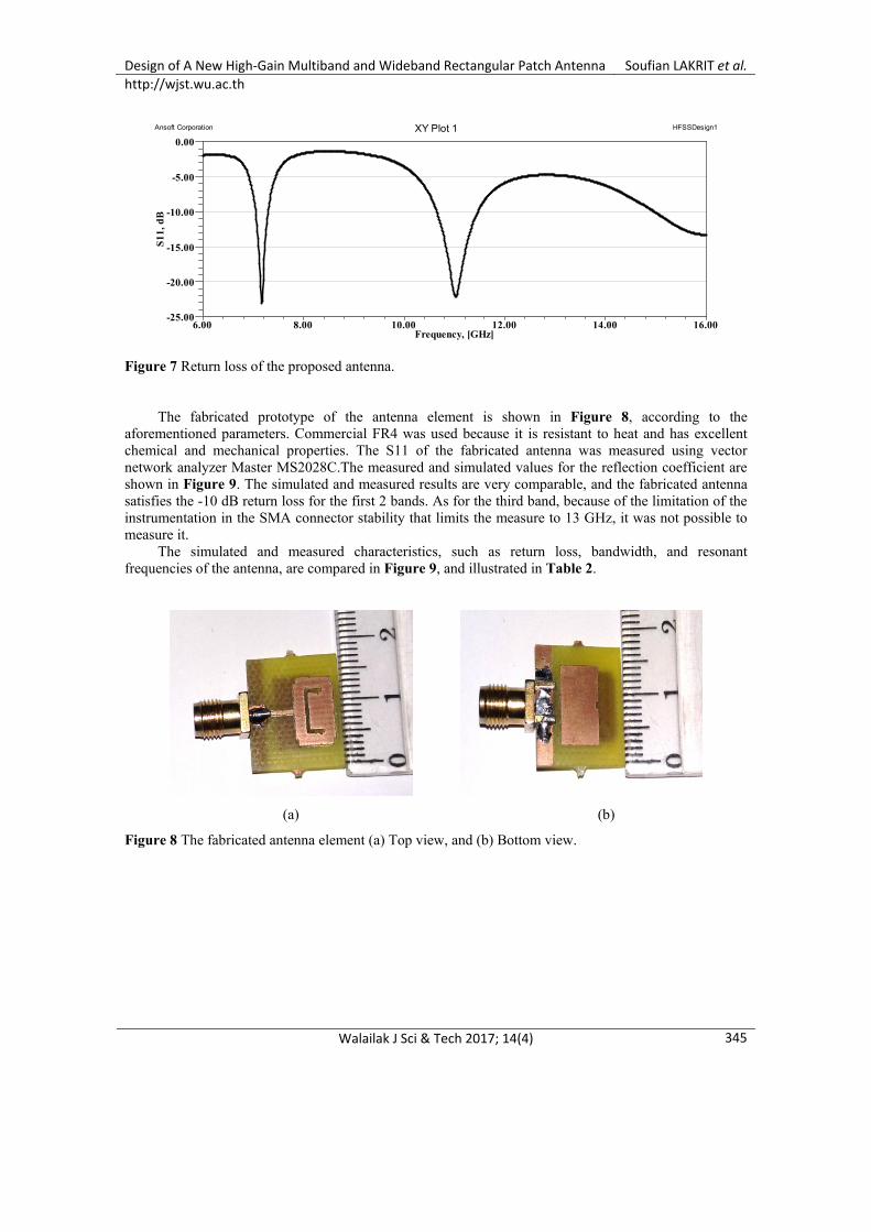
Figure 7 shows the variation of the antenna return loss as a function of frequency, simulated by HFSS, which uses finite elements method (FEM). The resonant frequencies are: 7.26 GHz, 11.03 GHz, and 15.96 GHz. Their respective return losses are: -23.5 dB, -22 dB, and -13 dB. The 3 frequency bands around these frequencies are: 7.15 GHz to 7.36 GHz, 10.72 GHz to 11.40 GHz, and 15.85 GHz to 16 GHz. This antenna can be used for radar and satellite applications.
Design of A New High-Gain Multiband and Wideband Rectangular Patch Antenna Soufian LAKRIT et al. http://wjst.wu.ac.th
Walailak J Sci & Tech 2017; 14(4)
345
Figure 7 Return loss of the proposed antenna.
The fabricated prototype of the antenna element is shown in Figure 8, according to the
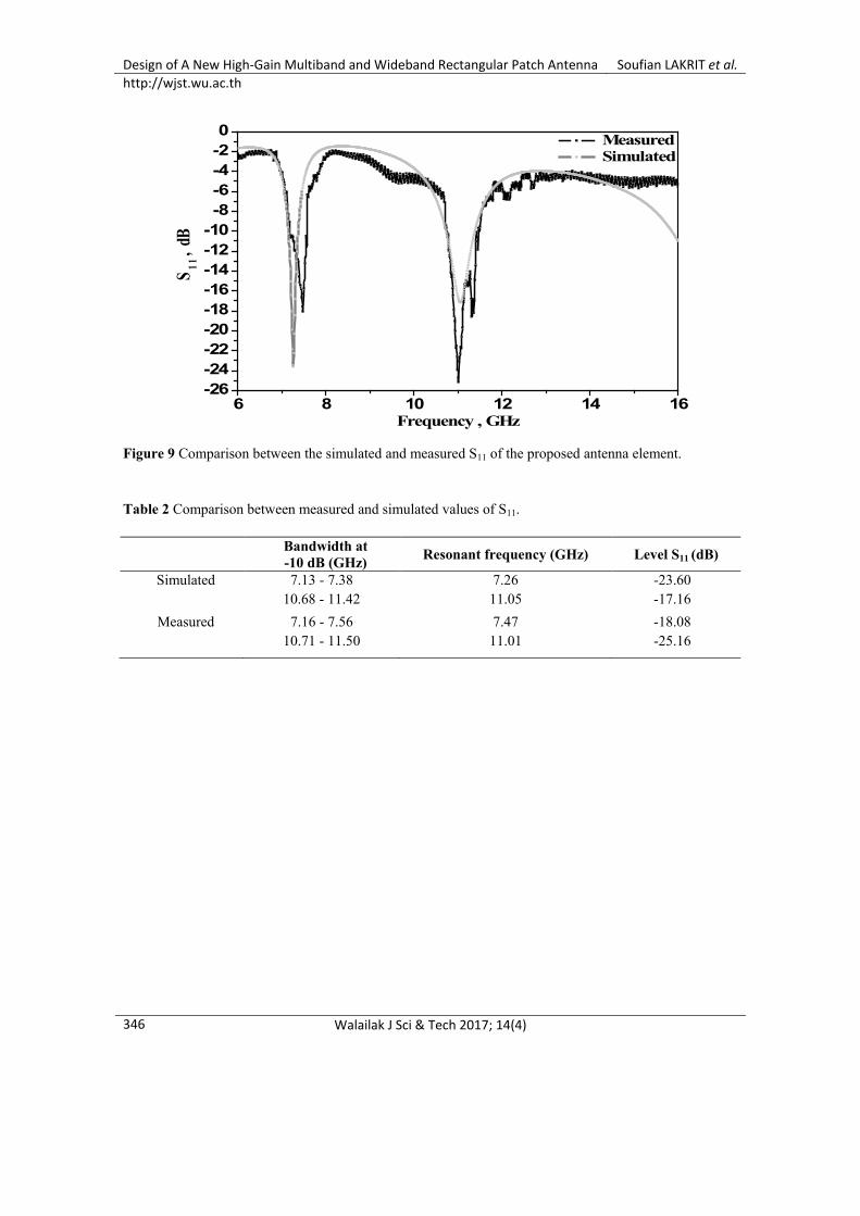
aforementioned parameters. Commercial FR4 was used because it is resistant to heat and has excellent chemical and mechanical properties. The S11 of the fabricated antenna was measured using vector network analyzer Master MS2028C.The measured and simulated values for the reflection coefficient are shown in Figure 9. The simulated and measured results are very comparable, and the fabricated antenna satisfies the -10 dB return loss for the first 2 bands. As for the third band, because of the limitation of the instrumentation in the SMA connector stability that limits the measure to 13 GHz, it was not possible to measure it.
The simulated and measured characteristics, such as return loss, bandwidth, and resonant frequencies of the antenna, are compared in Figure 9, and illustrated in Table 2.
(a) (b)
Figure 8 The fabricated antenna element (a) Top view, and (b) Bottom view.
6.00 8.00 10.00 12.00 14.00 16.00Frequency, [GHz]
-25.00
-20.00
-15.00
-10.00
-5.00
0.00S1
1, d
B
Ansoft Corporation HFSSDesign1XY Plot 1
Design of A New High-Gain Multiband and Wideband Rectangular Patch Antenna Soufian LAKRIT et al. http://wjst.wu.ac.th
Walailak J Sci & Tech 2017; 14(4) 346
Figure 9 Comparison between the simulated and measured S11 of the proposed antenna element.
Table 2 Comparison between measured and simulated values of S11.
Bandwidth at -10 dB (GHz) Resonant frequency (GHz) Level S11 (dB)
Simulated 7.13 - 7.38 10.68 - 11.42
7.26 11.05
-23.60 -17.16
Measured 7.16 - 7.56 10.71 - 11.50
7.47 11.01
-18.08 -25.16
6 8 10 12 14 16-26-24-22-20-18-16-14-12-10-8-6-4-20 Measured
Simulated
S 1 1 ,
dB
Frequency , GHz
Design of A New High-Gain Multiband and Wideband Rectangular Patch Antenna Soufian LAKRIT et al. http://wjst.wu.ac.th
Walailak J Sci & Tech 2017; 14(4)
347
(a) (b)
(c)
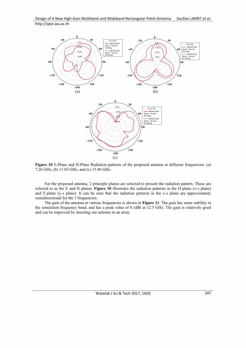
Figure 10 E-Plane and H-Plane Radiation patterns of the proposed antenna at different frequencies: (a) 7.26 GHz, (b) 11.03 GHz, and (c) 15.96 GHz.
For the proposed antenna, 2 principle planes are selected to present the radiation pattern. These are referred to as the E and H planes. Figure 10 illustrates the radiation patterns in the H-plane (x-z plane) and E-plane (y-z plane). It can be seen that the radiation patterns in the x-z plane are approximately omnidirectional for the 3 frequencies.
The gain of the antenna at various frequencies is shown in Figure 11. The gain has some stability in the simulation frequency band, and has a peak value of 6.1dBi at 12.5 GHz. The gain is relatively good and can be improved by inserting our antenna in an array.
-18.80
-15.60
-12.40
-9.20
90
60
300
-30
-60
-90
-120
-150-180
150
120
Curve Info
dB(GainTotal)Setup1 : Sw eep1Phi='0deg'
dB(GainTotal)Setup1 : Sw eep1Phi='90deg'
-14.00
-12.00
-10.00
-8.00
90
60
300
-30
-60
-90
-120
-150-180
150
120
Curve Info
dB(GainTotal)Setup1 : Sw eep1Phi='0deg'
dB(GainTotal)Setup1 : Sw eep1Phi='90deg'
-20.00
-15.00
-10.00
-5.00
90
60
300
-30
-60
-90
-120
-150-180
150
120
Curve Info
dB(GainTotal)Setup1 : Sw eep1Phi='0deg'
dB(GainTotal)Setup1 : Sw eep1Phi='90deg'

Design of A New High-Gain Multiband and Wideband Rectangular Patch Antenna Soufian LAKRIT et al. http://wjst.wu.ac.th
Walailak J Sci & Tech 2017; 14(4) 348
Figure 11 Gain of the antenna at different frequencies.
Antenna array design In this section, we study the duplication of our antenna 4 times to form a linear array. The purpose
of this task is to improve the radiation gain in order to have a more directional pattern. The array is presented in Figure 12. The radiating elements are connected by a feeding power divider. The array area is 26×78 mm2, with a separation distance of 0.48 𝜆 between the elements at 10 GHz.
(a)
(b)
Figure 12 Geometry of the antenna linear array, (a) Top view, (b) Bottom view.
D
Design of A New High-Gain Multiband and Wideband Rectangular Patch Antenna Soufian LAKRIT et al. http://wjst.wu.ac.th
Walailak J Sci & Tech 2017; 14(4)
349
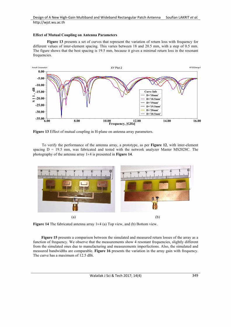
Effect of Mutual Coupling on Antenna Parameters
Figure 13 presents a set of curves that represent the variation of return loss with frequency for different values of inter-element spacing. This varies between 18 and 20.5 mm, with a step of 0.5 mm. The figure shows that the best spacing is 19.5 mm, because it gives a minimal return loss in the resonant frequencies.
Figure 13 Effect of mutual coupling in H-plane on antenna array parameters.
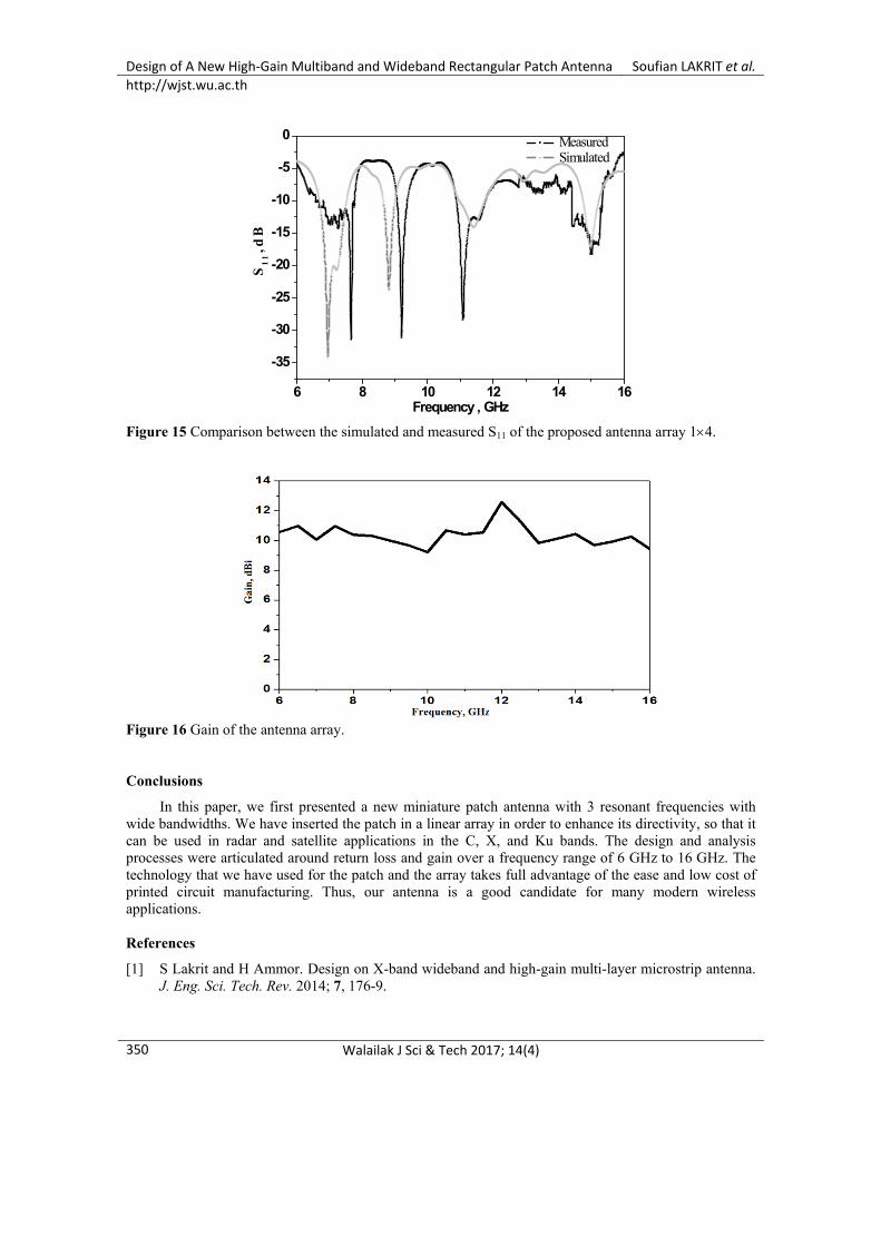
To verify the performance of the antenna array, a prototype, as per Figure 12, with inter-element spacing D = 19.5 mm, was fabricated and tested with the network analyzer Master MS2028C. The photography of the antenna array 1×4 is presented in Figure 14.
(a) (b)
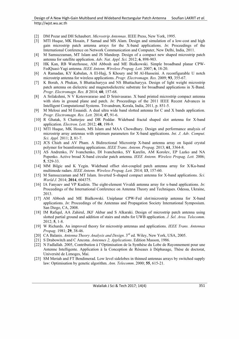
Figure 14 The fabricated antenna array 1×4 (a) Top view, and (b) Bottom view. Figure 15 presents a comparison between the simulated and measured return losses of the array as a
function of frequency. We observe that the measurements show 4 resonant frequencies, slightly different from the simulated ones due to manufacturing and measurements imperfections. Also, the simulated and measured bandwidths are comparable. Figure 16 presents the variation in the array gain with frequency. The curve has a maximum of 12.5 dBi.
6.00 8.00 10.00 12.00 14.00 16.00Frequency, [GHz]
-35.00
-30.00
-25.00
-20.00
-15.00
-10.00
-5.00
0.00
S 1
1 ,
dB
Ansoft Corporation HFSSDesign1XY Plot 2
Curve InfoD='18mm'D='18.5mm'D='19mm'D='19.5mm'D='20mm'D='20.5mm'
Design of A New High-Gain Multiband and Wideband Rectangular Patch Antenna Soufian LAKRIT et al. http://wjst.wu.ac.th
Walailak J Sci & Tech 2017; 14(4) 350
Figure 15 Comparison between the simulated and measured S11 of the proposed antenna array 1×4.
Figure 16 Gain of the antenna array. Conclusions
In this paper, we first presented a new miniature patch antenna with 3 resonant frequencies with wide bandwidths. We have inserted the patch in a linear array in order to enhance its directivity, so that it can be used in radar and satellite applications in the C, X, and Ku bands. The design and analysis processes were articulated around return loss and gain over a frequency range of 6 GHz to 16 GHz. The technology that we have used for the patch and the array takes full advantage of the ease and low cost of printed circuit manufacturing. Thus, our antenna is a good candidate for many modern wireless applications. References
[1] S Lakrit and H Ammor. Design on X-band wideband and high-gain multi-layer microstrip antenna. J. Eng. Sci. Tech. Rev. 2014; 7, 176-9.
6 8 10 12 14 16
-35
-30
-25
-20
-15
-10
-5
0 Measured Simulated
S 1
1 , d
B
Frequency , GHz
Design of A New High-Gain Multiband and Wideband Rectangular Patch Antenna Soufian LAKRIT et al. http://wjst.wu.ac.th
Walailak J Sci & Tech 2017; 14(4)
351
[2] DM Pozar and DH Schaubert. Microstrip Antennas. IEEE Press, New York, 1995. [3] MTI Huque, MK Hosain, F Samad and MS Alam. Design and simulation of a low-cost and high
gain microstrip patch antenna arrays for the X-band applications. In: Proceedings of the International Conference on Network Communication and Computer, New Delhi, India, 2011.
[4] M Samsuzzaman, MT Islam and JS Mandeep. Design of a compact new shaped microstrip patch antenna for satellite application. Adv. Nat. Appl. Sci. 2012; 6, 898-903.
[5] HK Kan, RB Waterhouse, AM Abbosh and ME Bialkowski. Simple broadband planar CPW-FedQuasi-Yagi antenna. IEEE Antenn. Wireless Propag. Lett. 2007; 6, 18-20.
[6] A Ramadan, KY Kabalan, A El-Hajj, S Khoury and M Al-Husseini. A reconfigurable U notch microstrip antenna for wireless applications. Progr. Electromagn. Res. 2009; 93, 355-67.
[7] K Borah, A Phukan, S Bhattacharyya and NS Bhattacharyya. Design of light weight microstrip patch antenna on dielectric and magnetodielectric substrate for broadband applications in X-Band. Progr. Electromagn. Res. B 2014; 60, 157-68.
[8] A Srilakshmi, N V Koteswararao and D Srinivasarao. X band printed microstrip compact antenna with slots in ground plane and patch. In: Proceedings of the 2011 IEEE Recent Advances in Intelligent Computational Systems. Trivandrum, Kerala, India, 2011, p. 851-5.
[9] M Meloui and M Essaaidi. A dual ultra wide band slotted antenna for C and X bands application. Progr. Electromagn. Res. Lett. 2014; 47, 91-6.
[10] R Ghatak, S Chatterjee and DR Poddar. Wideband fractal shaped slot antenna for X-band application. Electron. Lett. 2012; 48, 198-9.
[11] MTI Huque, MK Hosain, MS Islam and MAA Chowdhury. Design and performance analysis of microstrip array antennas with optimum parameters for X-band applications. Int. J. Adv. Comput. Sci. Appl. 2011; 2, 81-7.
[12] JCS Chieh and AV Pham. A Bidirectional Microstrip X-band antenna array on liquid crystal polymer for beamforming applications. IEEE Trans. Antenn. Propag. 2013; 61, 3364-8.
[13] AS Andrenko, IV Ivanchenko, DI Ivanchenko, SY Karelin, AM Korolev, EP Lazko and NA Popenko. Active broad X-band circular patch antenna. IEEE Antenn. Wireless Propag. Lett. 2006; 5, 529-33.
[14] MM Bilgic and K Yegin. Wideband offset slot-coupled patch antenna array for X/Ku-band multimode radars. IEEE Antenn. Wireless Propag. Lett. 2014; 13, 157-60.
[15] M Samsuzzaman and MT Islam. Inverted S-shaped compact antenna for X-band applications. Sci. World J. 2014; 2014, 604375.
[16] IA Fanyaev and VP Kudzin. The eight-element Vivaldi antenna array for x-band applications. In: Proceedings of the International Conference on Antenna Theory and Techniques. Odessa, Ukraine, 2013.
[17] AM Abbosh and ME Bialkowski. Uniplanar CPW-Fed slot/microstrip antenna for X-band applications. In: Proceedings of the Antennas and Propagation Society International Symposium. San Diego, CA, 2008.
[18] IM Rafiqul, AA Zahirul, JKF Akbar and S Alkaraki. Design of microstrip patch antenna using slotted partial ground and addition of stairs and stubs for UWB application. J. Sel. Area. Telecomm. 2012; 5, 1-8.
[19] W Richards. An improved theory for microstrip antennas and applications. IEEE Trans. Antennas Propag. 1981; 29, 38-46.
[20] CA Balanis. Antenna Theory Analysis and Design. 3rd ed. Wiley, New York, USA, 2005. [21] S Drabowitch and C Ancona. Antennes 2, Applications. Edition Masson, 1986. [22] N Fadlallah. 2005, Contribution à l’Optimisation de la Synthèse du Lobe de Rayonnement pour une
Antenne Intelligente. Application à la Conception de Réseaux à Déphasage, Thèse de doctorat, Université de Limoges, Mai.
[23] SM Meriah and FT Bendimerad. Low level sidelobes in thinned antennas arrays by switched supply law: Optimisation by genetic algorithm. Ann. Telecomm. 2000; 55, 615-21.