Embed Size (px)
Citation preview
0
DESIGN OF A PHASE LOCKED LOOP FOR OPTICAL
UPCONVERSION
A Master's Thesis Submitted to the Faculty of the
Escola Tècnica d'Enginyeria de Telecomunicació de Barcelona
Universitat Politècnica de Catalunya by
FRANCISCO HERRANZ SALAZAR
In partial fulfillment of the requirements for the degree of
MASTER IN TELECOMMUNICATIONS ENGINEERING
Advisor: Bart Kuyken
Co-Advisor: Jose Antonio Lázaro Villa
Barcelona, May 2018

I
II
Title of the thesis: Design of a phase locked loop for optical upconversion.
Author: Francisco Herranz Salazar
Advisors: Bart Kuyken, Jose Antonio Lázaro Villa
Abstract
Silicon Photonics has become a key technology in the design of devices for the next generation of wireless communications. One of the most important challenges of 5G is the transport of microwave signals over fiber links, in what are known as Radio over Fiber systems. Optical Phase Lock Loop (OPLL) is positioning itself as one of the most relevant techniques for the generation of stable GHz signals. In this thesis, the different elements that form an OPLL are analyzed in both the optical and electrical domains. A SIMULINK model for an OPLL that reaches stable operation at frequencies between 3 and 10 GHz is obtained. Also, the suitability of a novel Semiconductor Laser structure that acts as a Phase Modulator is analyzed with three different software tools that study the modulation process form the carrier concentration to the effective index change.

III
To my grandparents. Eusebia, Sotero, Ángel and Pilar. Thank you for making me who I am today.

IV
Acknowledgements
I would first like to thank my Thesis advisor, professor Bart Kuyken form Ghent Universiteit, for proposing this topic for the Thesis and allowing me to work on it. I would also like to thank professor Guy Torfs, who acted as advisor for all the electronic topics of this Thesis. It would have not been possible without their guidance.
I must also express my most sincere gratitude to PhD Students Camiel Op de Beeck and Marijn Verbeke. They always had the time and patience to explain those topics that required more expertise and provided support when it was most needed.
It is also important to give thanks to professor Jose Antonio Lázaro Villa from Universitat Politècnica de Catalunya. He was the one who proposed carrying out my Master Thesis in Ghent and I will be forever grateful to him for that. Also, many thanks for the multiple times we collaborated during my academic years. Working with him developed my passion for academic research.
On a more personal note, I am extremely grateful to all the friends with whom I have shared the last two years. This MsC Degree has been quite a challenge, and it would have been much more complicated without everyone that provided support.
And last but not least, to my parents, sister and brother-in-law. They were the first ones to show support during the bad days, and to celebrate during the good ones.
V
Revision history and approval record
Revision Date Purpose
0 03/03/2018 Document creation
1 12/04/2018 Document revision 1
2 24/04/2018 Document revision 2
Written by: Reviewed and approved by:
Date 15/05/2018 Date 02/05/2018
Name Francisco Herranz Salazar Name Jose Antonio Lázaro
Position Project Author Position Project Supervisor
VI
Table of contents
Abstract ............................................................................................................................ IIAcknowledgements ......................................................................................................... IVRevision history and approval record ................................................................................VTable of contents ............................................................................................................. VIList of Figures ................................................................................................................ VIIIList of Tables ................................................................................................................... XI1. Introduction ................................................................................................................ 1
1.1. Statement of purpose .......................................................................................... 11.2. Developed tasks.................................................................................................. 3
2. State of the art of the technology used or applied in this thesis .................................. 42.1. Radio over Fiber systems .................................................................................... 42.2. Photonic techniques for millimeter wave signal generation .................................. 52.3. Optical Phase Lock Loop .................................................................................... 62.4. Semiconductor Lasers......................................................................................... 8
2.4.1. III-V/Si Phase Modulators ............................................................................. 93. Project development ................................................................................................ 11
3.1. Phase Locked Loop modeling ........................................................................... 113.1.1. Steady state behavior and transient response of Phase Locked Loops ...... 13
3.1.1.1. Phase step in the reference signal .......................................................... 143.1.1.2. Frequency step in the reference signal.................................................... 15
3.1.2. Stability Analysis of PLLs ............................................................................ 153.2. Optical source analysis ..................................................................................... 16
3.2.1. Thermal and electronic contributions to the Frequency Modulation ............. 173.2.2. Presence of undesired Amplitude Modulation component ........................... 18
3.2.2.1. Extraction of Amplitude Modulation depth ............................................... 203.2.2.2. Extraction of the Phase Modulation depth ............................................... 21
3.2.3. Hybrid III-V/Si MOS modulators .................................................................. 233.2.3.1. Developed model for the calculation of phase shift ................................. 26
4. Results .................................................................................................................... 314.1. Basic PLL analysis ............................................................................................ 314.2. New PLL topology ............................................................................................. 324.3. Optical Source analysis ..................................................................................... 40

VII
5. Conclusions and future development ....................................................................... 45Bibliography ................................................................................................................... 47Appendices .................................................................................................................... 51Glossary ......................................................................................................................... 56
VIII
List of Figures
Fig. 1 Role of mmWave in Multi-Connectivity Network. From [1]....................................... 1Fig. 2 Schematic of an OPLL. ........................................................................................... 2Fig. 3 Radio over Fiber (RoF) based systems for mobile networks. From [10]. ................. 4Fig. 4 Schematic of an OPL. ............................................................................................. 6Fig. 5 Experimentally measured FM response of a commercial DFB laser with a
theoretical fit using a Low Pass Filter model. From [23]. ............................................ 7Fig. 6 Cross section of the laser structure. ........................................................................ 8Fig. 7 Layout of the DFB laser. From [27]. ........................................................................ 9Fig. 8 Electron-induced refractive index changes of InGaAsP, InP and Si. From [28]. ...... 9Fig. 9 Diagram of a Phase Locked Loop. ........................................................................ 11Fig. 10 SIMULINK Schematic of a basic PLL. ................................................................. 13Fig. 11 Basic waveforms of a locked PLL. From top to bottom, Reference signal, VCO
output and PD output. ............................................................................................. 14Fig. 12 SIMULINK schematic of a PLL in the phase domain. .......................................... 15Fig. 13 Magnitude and phase of the FM response. From [31]. ........................................ 18Fig. 14 Setup used to measure the response of the DFB. .............................................. 20Fig. 15 Simulation of the beat note between an AM signal and a reference signal. ......... 20Fig. 16 Experimental data of the beat note between a signal modulated at 50 MHz and 0
dBm and a reference signal. .................................................................................... 21Fig. 17 Obtained AM gain as a function of modulation amplitude for different modulation
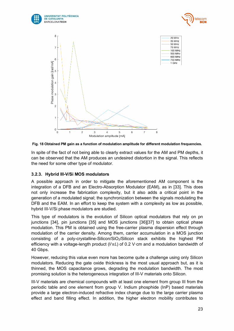
frequencies.............................................................................................................. 22Fig. 18 Obtained PM gain as a function of modulation amplitude for different modulation
frequencies.............................................................................................................. 23Fig. 19 Variation of the refractive index of Silicon considering only plasma effect (red) and
using experimental equations (blue). ....................................................................... 25Fig. 20 Variation of the refractive index of InGaAsP considering only plasma effect (red)
and considering also other effects (blue). ................................................................ 25Fig. 21 Diagram of the developed model. ....................................................................... 26Fig. 22 Representation in DEVICE of the structure from [29]. ......................................... 26Fig. 23 Flow diagram of the MATLAB routine that calculates the refractive index change.
................................................................................................................................ 28Fig. 24 Visualization of the refractive index along the InGaAsP layer provided by MODE.
................................................................................................................................ 29Fig. 25 Visualization of the refractive index along the Silicon layer provided by MODE. . 29Fig. 26 Effective index change (blue) and Phase shift (red) for different voltages. .......... 30
IX
Fig. 27 From top to bottom, outputs of the reference and VCO, PD and Control Signal. . 31Fig. 28 Bode diagrams of basic PLL. .............................................................................. 32Fig. 29 Original first order filter (left) and improved second order filter (right). ................. 33Fig. 30 Theoretical Bode diagram of the PLL's open loop transfer function. From [41].... 33Fig. 31 Open Loop transfer function of the PLL. ............................................................. 34Fig. 32 Closed loop transfer function of the PLL. ............................................................ 34Fig. 33 Final SIMULINK model of the OPLL. .................................................................. 35Fig. 34 Detailed illustration of the PD model. .................................................................. 36Fig. 35 Ideal (blue) and filtered (yellow) output of the PD. .............................................. 37Fig. 36 Input (blue) and output (yellow) of the LPF. ........................................................ 37Fig. 37 Modeling of the modulating of the SL. ................................................................. 38Fig. 38 Locked signal (blue) and reference signal (yellow).............................................. 38Fig. 39 Evolution of the Hold-in range for the frequencies in the Acquisition range. ........ 39Fig. 40 Control signal unable to reach steady state. ....................................................... 40Fig. 41 Control signal when locking is achieved first for 7 GHz and then for 8 GHz. ....... 40Fig. 42 Representation of the simulated structure. .......................................................... 41Fig. 43 Visualization of the grating area below the BCB layer. ........................................ 41Fig. 44 Hole concentration in the area below the BCB layer for 0 V. Perspective view (top),
Top view (bottom left), Cross-section view (bottom right). ....................................... 42Fig. 45 Hole concentration along the Y coordinate for 0 V. ............................................. 43Fig. 46 Hole concentration along the Z coordinate for 0 V. ............................................. 43Fig. 47 Hole concentration along the z coordinate for 1 V. .............................................. 44Fig. 48 Hole concentration along the z coordinate for 3 V. .............................................. 44Fig. 49 Points for which the electron concentration in the InGaAsP is calculated (green).
................................................................................................................................ 51Fig. 50 Points for which the hole concentration in the Si is calculated (green). ............... 51Fig. 51 Carrier concentrations for an applied voltage of 1.47 V. ...................................... 52Fig. 52 Carrier concentration for an applied voltage of 3.15 V. ....................................... 52Fig. 53 Carrier concentration level after interpolation in the InGaAsP (top) and Si (bottom)
for 1.47 V................................................................................................................. 53Fig. 54 Carrier concentration level after interpolation in the InGaAsP (top) and Si (bottom)
for 3.15 V................................................................................................................. 53Fig. 55 Refractive index change using the interpolated carrier concentrations for 1.47 V.
................................................................................................................................ 54Fig. 56 Refractive index change using the interpolated carrier concentrations for 3.15 V.
................................................................................................................................ 54

X
Fig. 57 Final refractive index profile for 1.47 V. ............................................................... 55Fig. 58 Final refractive index profile for 3.15 V. ............................................................... 55

XI
List of Tables
Table 1 Comparison between components of PLLs and OPLLs ..................................... 11Table 2 List of parameters of basic PLL.......................................................................... 13Table 3 List of used devices. .......................................................................................... 19Table 4 List of parameters and values of the simulation. ................................................ 27Table 5 Frequency limits of each Hold-in range. ............................................................. 39Table 6 Parameter values of the implemented structure in DEVICE. .............................. 41
1
1. Introduction
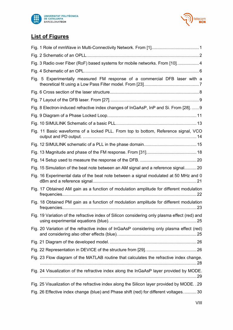
1.1. Statement of purpose The fifth generation of mobile networks (5G) is on the horizon and it promises to deliver a unifying connectivity fabric that will take on a much larger role than previous generations. This new kind of network will not only interconnect people, but also control machines, objects and devices.
Making this vision a reality will require a unified, more capable radio interface design that will bring new levels of flexibility, scalability and efficiency to meet the ever-expanding connectivity requirements. 5G must adapt to support traffic from sensors at data rates as low as tenths of kbps as well as traffic from new mobile experiences at data rates up to 10 Gbps. New technologies are being developed in order to enhance mobile broadband with new levels of performance and efficiency such as Small Cells, massive MIMO and usage of Millimeter-Wave (mmWave) frequency bands (30 – 300 GHz). Nevertheless, reducing the size of the cells, hence increasing the number of antennas, is not a cost-efficient solution. The use of mmWave radio will be an important part of future 5G networks, but it is not the entirety of 5G. As seen in Fig.1, the new radio interface will operate in multiple frequency bands, being mmWave (5G above 6GHz) one of them.
Fig. 1 Role of mmWave in Multi-Connectivity Network. From [1].
Different mmWave bands have been proposed for high-capacity wireless systems employing Radio-over-Fiber (RoF); in the 24 to 30 GHz band [2], 75 to 110 GHz [3], and at 120 GHz [4][5]. However, the band that has attracted major interest is around 60 GHz because of two reasons. The first one is that this frequency is the same as that of the oxygen absorption peak, which results in high atmospheric attenuation1. The second one is that in North America, there is a 7 GHz frequency space of unlicensed spectrum around 60 GHz that overlaps with unlicensed spectra in Europe, Japan and Australia, which opens the opportunity to worldwide standardization.
Photonic techniques have become key enablers to unlock future broadband wireless communications with multigigabit data rates. Generation of mmWave signals using both electronic and photonic approaches has already been demonstrated [6]. Photonic approaches have some inherent advantages such as being widely tunable, having ultra-high bandwidth and with the ability to be seamlessly connected to wired networks. There are multiple optical signal generation techniques, the most promising of which is Optical
1 High atmospheric attenuation allows reduction in both the cell size and frequency reuse distance in cellular systems.
2
Heterodyning. This method consists of two optical sources generating signals at two different wavelengths that are mixed into a photodiode or photoconductor. The generated signal is an electrical beat-note at a frequency given by the difference between the wavelengths.
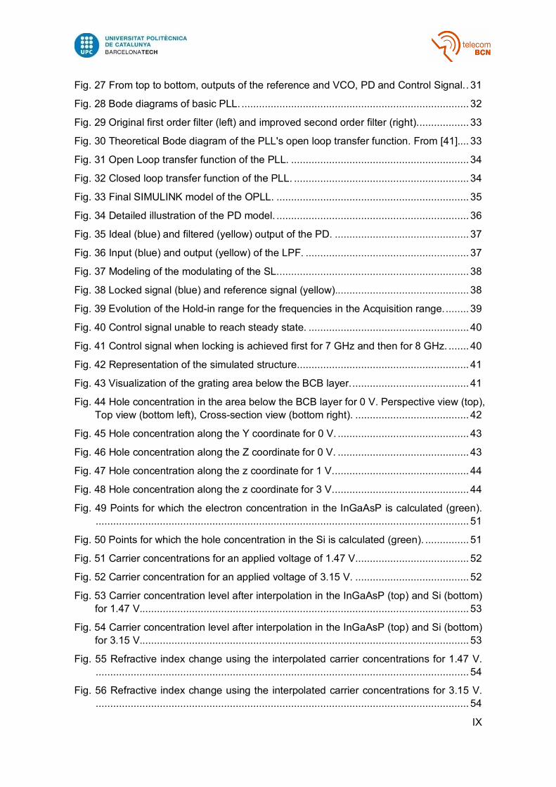
The most commonly used optical source is a Semiconductor Laser (SCL), which may have a linewidth of tens of MHz and whose frequency is characterized by a low stability caused by the laser’s thermal drift and its mode changes. This means that phase stabilization techniques must be developed. This thesis focuses on different aspects of one of these techniques, the Optical Phase Lock Loop (OPLL).
As it can be observed in Fig. 2, an OPLL is a negative-feedback control system that provides phase stabilization, where a Slave Laser (SL) acts as a Current Controlled Oscillator (CCO) that tracks the phase and frequency of a Master Laser (ML). By using a Radiofrequency Oscillator as a reference, the Slave Laser can be locked to the Master Laser with a controlled offset.
Fig. 2 Schematic of an OPLL.
OPLL is considered one of the most promising techniques, since it allows offset phase locking, which enables adjustable frequency spacing between the lasers. It also has the potential of being applied as an elementary building block in many photonic systems where active, narrow bandwidth, high-rejection filters are required.
One of the key questions that remain when designing an OPLL is the choice of the SL. Different mmWave and Terahertz photonic integrated sources have been demonstrated based on different light sources: Distributed Bragg Reflectors (DBR) [7][8] or Distributed Feedback (DFB) lasers [9]. Among the benefits of this last type of laser diodes, the most important ones are that they are the simplest ones to analyze and fabricate and its very large current-frequency sensitivity.
Nevertheless, there are also considerable shortcomings. When operating an SCL as an SL, the main interest will be in using the phase of the output signal to transmit information. However, Frequency Modulation (FM) in directly modulated DFB lasers is inherently coupled to an often-undesired Amplitude Modulation (AM) component. This shows the need of an external Phase Modulator. The first solution that may come to mind is using DFB lasers with integrated phase modulators, but these come along with complex fabrication issues and would reduce the cost-effectiveness to the system.
3
An alternative solution is the use of III-V/Silicon hybrid MOS modulators, due to the large electron-induced refractive index change in these materials. In addition, the high electron mobility and the low carrier-plasma absorption of III-V compounds are beneficial for overcoming the trade-offs among voltage-length products.
Taking all the above into account, the goal of this thesis will be the design of an Optical Phase Lock Loop structure that uses a DFB laser as a Current Controlled Oscillator (CCO). In the process, the design of the feedback electronics and of the analysis of available optical sources will be of fundamental significance. The OPLL designed should be able to work in the lower GHz range (around 3 GHz), acting as a baseline for a future development of an OPLL able to actually work in the mmWave range (around 30 GHz). In addition, the locking should be achieved with offsets between the ML and the SL on the order of several GHz.
1.2. Developed tasks Optical Phase Lock Loops can be understood as an optical modification of traditional all-electronic Phase Locked Loops (PLL). Bearing this in mind, the design and analysis of the different components of the OPLL are separately studied in the electrical and optical domains.
Firstly, the design of an all-electronic PLL is carried out. This involves the analysis of basic PLL structures and its feasibility for operation in the lower GHz frequency range. The design of the Phase Detector and the Loop Filter is addressed. This PLL design is performed using software tools such as MATLAB and SIMULINK.
Trying to achieve a cost-effective solution, a DFB laser already fabricated is used as a candidate for the CCO. It is characterized by measuring its Amplitude and Frequency Modulation levels and its feasibility for its use as a phase modulator is evaluated.
Also, the case of Phase Modulators based on III-V and Silicon MOS capacitors is studied. A MATLAB model is developed in order to calculate the refractive index change that a certain carrier concentration level variation causes. With this model, a novel structure is analyzed as a second candidate for the CCO.
4
2. State of the art of the technology used or applied in this thesis
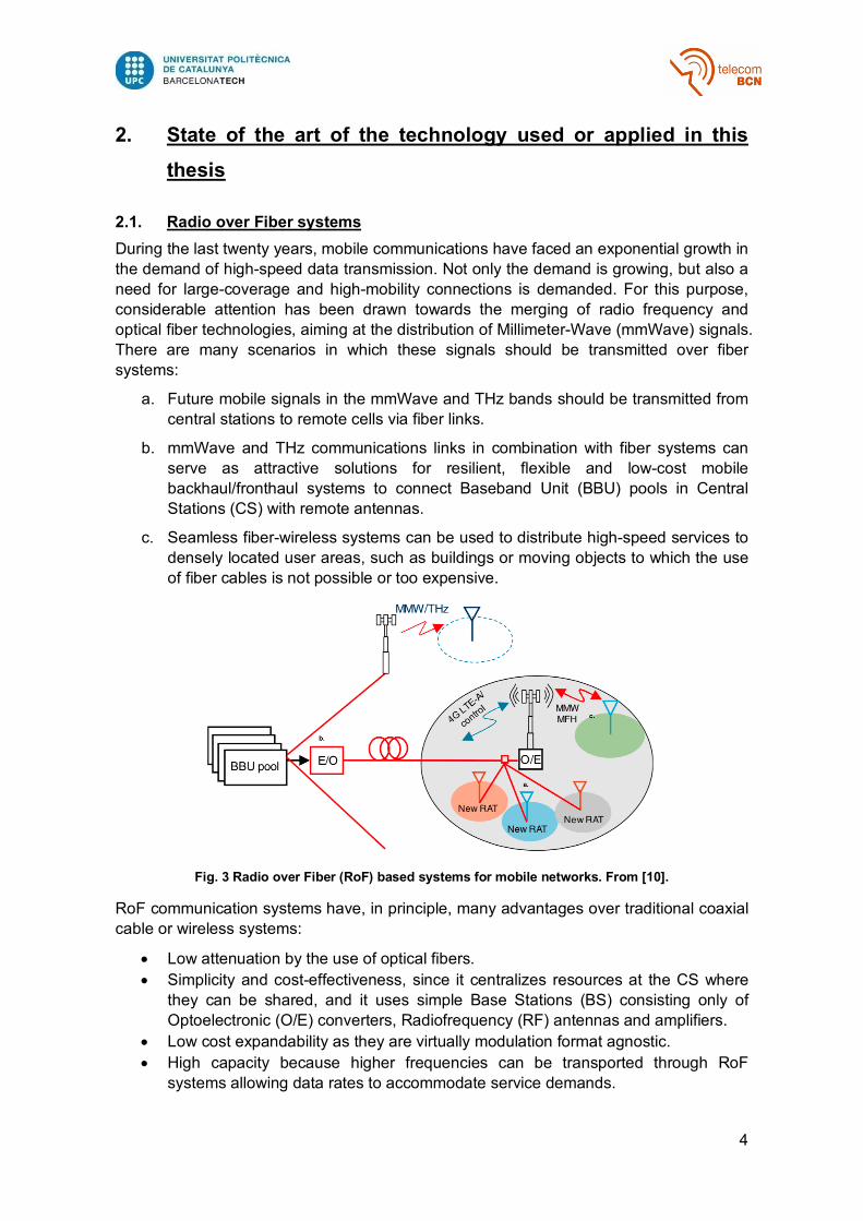
2.1. Radio over Fiber systems During the last twenty years, mobile communications have faced an exponential growth in the demand of high-speed data transmission. Not only the demand is growing, but also a need for large-coverage and high-mobility connections is demanded. For this purpose, considerable attention has been drawn towards the merging of radio frequency and optical fiber technologies, aiming at the distribution of Millimeter-Wave (mmWave) signals. There are many scenarios in which these signals should be transmitted over fiber systems:
a. Future mobile signals in the mmWave and THz bands should be transmitted from central stations to remote cells via fiber links.
b. mmWave and THz communications links in combination with fiber systems can serve as attractive solutions for resilient, flexible and low-cost mobile backhaul/fronthaul systems to connect Baseband Unit (BBU) pools in Central Stations (CS) with remote antennas.
c. Seamless fiber-wireless systems can be used to distribute high-speed services to densely located user areas, such as buildings or moving objects to which the use of fiber cables is not possible or too expensive.
Fig. 3 Radio over Fiber (RoF) based systems for mobile networks. From [10].
RoF communication systems have, in principle, many advantages over traditional coaxial cable or wireless systems:
• Low attenuation by the use of optical fibers. • Simplicity and cost-effectiveness, since it centralizes resources at the CS where
they can be shared, and it uses simple Base Stations (BS) consisting only of Optoelectronic (O/E) converters, Radiofrequency (RF) antennas and amplifiers.
• Low cost expandability as they are virtually modulation format agnostic. • High capacity because higher frequencies can be transported through RoF
systems allowing data rates to accommodate service demands.
5
• Flexibility that comes from allowing independent infrastructure providers and multi-service operation at the same RoF network.
• Dynamic resource allocation, since functions as switching, modulation and others are performed at the CS.
On the other hand, major drawbacks are that, as the RF frequency increases, so does the requirement for high-speed optical components, more sophisticated mmWave generation techniques, and a larger number of BSs with high bandwidth Photodetectors to cover a service area. Moreover, effects of dispersion across the Optical Distribution Network (ODN) become a problem even over relatively short fibers. Therefore, advanced modulation and transmission schemes are required.
The encapsulation of signals in traditional Microwave bands into mmWave bands using photonic techniques would be very attractive for flexible, low-latency mobile fronthaul systems. Schemes such as those proposed in [11] demonstrate that mmWave signal generation can be performed by optical upconversion to the mmWave/THz band by photomixing radio signals with an optical two-tone signal. However, using high-precision optical modulation is of the most significance to generate a frequency and phase-stabilized optical mmWave signal.
2.2. Photonic techniques for millimeter wave signal generation Several demonstrations have been presented for the generation of signals in the millimeter/sub-millimeter range using photonic approaches. The two key components are optical sources and optical-to-electrical converters.
The most promising optical signal generation technique is Optical Heterodyning. This method requires mixing two signals with different wavelengths from two uncorrelated sources on a photodiode. This process generates an electrical signal at a frequency given by the difference between the wavelengths, which is referred to as beat-note. Since the two optical signals come from uncorrelated sources, the generated beat note exhibits considerable phase fluctuations due to the linewidth of the lasers and to the relative thermal drift of the wavelength between them.
These fluctuations reflect the need of some sort of phase stabilization mechanism. Phase stabilization is achieved by controlling the difference between the phases of the signals being mixed using locking techniques such as, Optical Injection-Locking (OIL), Optical Phase Lock Loop (OPLL) and Optical Injection Phase-Lock Loop (OIPLL).
The last technique, Optical Injection Phase Lock Loop, is a combination of the other two. It suppresses wideband phase noise thanks to the injection-locking mechanism while the laser frequency drift and close-to-carrier phase noise are controlled through a phase-lock loop path. It has been studied for coherent receivers [12], satellite to ground communication [13] and high frequency signal synthesis [14]. While it proves promising and capable of overcoming the difficulties of the two other techniques, it also involves a higher complexity in its realization.
The first of these techniques, Optical Injection-Locking, has proven suitable for the generation of frequencies above 100 GHz by injection locking to spectral lines from an optical comb [15][16][17]. Nevertheless, due to its homodyne nature, its locking range is limited to a few hundreds of MHz.
6
The shortcomings of the aforementioned techniques make OPLL the most suitable technique, as it allows offset phase locking, thus enabling adjustable frequency spacing between the lasers. This is also the simplest solution in applications where an offset between the frequencies of the two optical signals, the beat note, is required. Such applications vary from high-purity mmWave and THz signal generation [19][20] or coherent Terahertz photonics [21] to precise measurements such as spectroscopy [22]. For instance, in [18], an OPLL that can be phase stabilized to the reference with an offset between 4 and 12 GHz is realized.
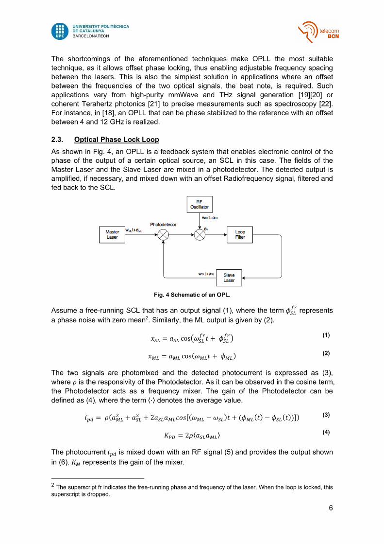
2.3. Optical Phase Lock Loop As shown in Fig. 4, an OPLL is a feedback system that enables electronic control of the phase of the output of a certain optical source, an SCL in this case. The fields of the Master Laser and the Slave Laser are mixed in a photodetector. The detected output is amplified, if necessary, and mixed down with an offset Radiofrequency signal, filtered and fed back to the SCL.
Fig. 4 Schematic of an OPL.
Assume a free-running SCL that has an output signal (1), where the term 𝜙"#$% represents
a phase noise with zero mean2. Similarly, the ML output is given by (2).
𝑥"# = 𝑎"# cos,𝜔"#$%𝑡 +𝜙"#
$%1 (1)
𝑥2# = 𝑎2# cos(𝜔2#𝑡 +𝜙2#) (2)
The two signals are photomixed and the detected photocurrent is expressed as (3), where 𝜌 is the responsivity of the Photodetector. As it can be observed in the cosine term, the Photodetector acts as a frequency mixer. The gain of the Photodetector can be defined as (4), where the term ⟨·⟩ denotes the average value.
𝑖:; = 𝜌(𝑎2#< + 𝑎"#< + 2𝑎"#𝑎2#𝑐𝑜𝑠[(𝜔2# − 𝜔"#)𝑡 + (𝜙2#(𝑡) − 𝜙"#(𝑡))]) (3)
𝐾EF = 2𝜌⟨𝑎"#𝑎2#⟩ (4)
The photocurrent 𝑖:; is mixed down with an RF signal (5) and provides the output shown in (6). 𝐾2 represents the gain of the mixer.
2 The superscript fr indicates the free-running phase and frequency of the laser. When the loop is locked, this superscript is dropped.
7
𝑥GH(𝑡) = 𝑎GH sin(𝜔GH𝑡 +𝜙GH) (5)
𝑖2(𝑡) = ±𝐾2𝐾EF𝑎GH𝑠𝑖𝑛[(𝜔2# − 𝜔"# ± 𝜔GH)𝑡 + (𝜙2#(𝑡) − 𝜙"#(𝑡) ± 𝜙GH)] (6)
For the sake of simplicity, only the positive sign is considered. The output 𝑖2 is fed into the SL, which acts as a Current Controlled Oscillator (CCO) whose frequency shift, Δ𝜔"# , is proportional to the input current.
Δ𝜔"# = 𝐾NNO𝑖2(𝑡) == 𝐾NNO𝐾2𝐾EF𝑎GH𝑠𝑖𝑛[(𝜔2# − 𝜔"# ± 𝜔GH)𝑡 + (𝜙2#(𝑡) − 𝜙"#(𝑡) ± 𝜙GH)]
(7)
In steady state operation, the output of the mixer (6) does not change with time and yields
𝜔"# = 𝜔2# + 𝜔GH (8)
𝜙P"# = 𝜙P2# + 𝜙PGH + 𝜙QR (9)
The parameter 𝜙QR is the steady phase error in the loop and it is a consequence of the feedback current keeping the loop in lock. As it can be observed, the optical phase of the SL can be controlled by adjusting the phase of the RF signal.
In [23], it is demonstrated that for a stable loop operation, it is necessary that the loop bandwidth be much larger than the summed linewidths of the two lasers. Even though the maximum achievable bandwidth is ultimately limited by the loop propagation delay, a more stringent limitation is imposed by the phase reversal in the Frequency Modulation (FM) response of single section SCLs.
From Fig. 5, it can be observed that the FM response of a commercial DFB laser can be modeled as a LPF. It is important to note that this is an effect that occurs at low frequencies, as opposed to high-speed free-carrier effects near the resonance frequency.
𝐹H2(𝑓) = 𝐾QU −𝐾VW
1 + Y𝑗 𝑓𝑓[
(10)
Fig. 5 Experimentally measured FM response of a commercial DFB laser with a theoretical fit using a
Low Pass Filter model. From [23].
8
In (10), the term 𝐾QU represents the broadband electronic response, the term 𝐾VW denotes the thermal response and 𝑓[ is the corner frequency of the thermal response. It is important to note that the two types of noise have opposite effects, resulting in a phase-reversal (change of 𝜋 radians). It is also pertinent to state that for commercial DFBs, 𝑓[ can reach values up to 100 MHz. The traditional solution to this problem is the use of multielectrode SCL, but they do not offer the simplicity of single section SCLs.
2.4. Semiconductor Lasers Nowadays, Silicon Photonics is the key technology for the integration of optical functions on a chip. It provides advantages such as compactness and availability of high-speed electronics. However, its main drawback is that it has an indirect bandgap, making monolithic laser integration onto Silicon Photonic Integrated Circuits (PICs) difficult. That is why high performance semiconductor lasers are realized using III-V compound semiconductors3. Therefore, there is a need to integrate III-V semiconductors on Silicon PICs.
The integration of III-V semiconductors can be made using different methods such as flip-chip integration [24], bonding approaches [25] and hetero-epitaxial growth [26]. In [27], a laser structure of III-V is designed using adhesive bonding for the integration onto Silicon. This method has advantages such as having more relaxed cleanliness and surface roughness requirements.
This laser uses DVS-BCB (divinylsiloxane-bis-benzocyclobutene) as the adhesive material, since it has low curing temperature, high degree of planarization, high optical clarity, good thermal stability, excellent chemical stability, low moisture absorption and wide applicability. Its main drawback is its low thermal conductivity but, for thicknesses below 100 nm, the Buried Oxide (BOX) is dominant in the thermal resistance of the device.
In Fig. 6, the cross section of this laser structure can be observed. From bottom to top, the different layers are the Silicon substrate, the BOX, the Silicon waveguide, the DVS-BCB, the different layer of III-V compound materials and the Gold (Au) used for the electrical contacts.
Fig. 6 Cross section of the laser structure.
3 Compound semiconductors are composed of elements of at least two different species. In the case of III-V, these elements are from groups 13 and 15.
9
Optical coupling between the III-V compound and the Silicon is realized through a taper based spot size converter structure. The optical mode is strongly confined to the III-V waveguide and a strong refractive index mismatch exists between the III-V and the silicon waveguides. By tapering the III-V and/or the Silicon waveguide, wave vector matching can occur and the optical mode can be gradually transferred to the silicon waveguide. In Fig. 7, an illustration of this laser structure used as a DFB laser is shown.
Fig. 7 Layout of the DFB laser. From [27].
2.4.1. III-V/Si Phase Modulators Most Silicon-based modulators suffer from low phase modulation efficiency, mainly due to the weak plasma dispersion effect in Silicon. It is essential to find a novel modulation scheme for Silicon Photonics.
In [28][29], several III-V compound and Silicon hybrid modulators are demonstrated. These devices provide large electron-induced refractive-index change due to the large carrier-plasma and band-filling effects. Also, the higher electron mobility contributes to reducing the carrier-plasma absorption loss and the resistance-capacitance time delay.
Mach-Zehnder Modulators consisting of a III-V pn diode on Silicon have already been developed, but the efficiency is still reduced because of the limited optical confinement in the III-V region. By introducing a III-V material into a MOS capacitor modulator, higher overlap between the optical intensity and carrier distribution in both the n-type III-V material and the p-type Silicon is achieved.
Fig. 8 Electron-induced refractive index changes of InGaAsP, InP and Si. From [28].
10
These modulators use the carrier-induced changes in the refractive index of both the Silicon and the III-V material in order to phase-modulate the lightwave. When a voltage is applied between the n-type III-V layer and the p-type Si layer, carriers accumulate at the III-V/Si interface, which contributes to optical phase modulation of the fundamental Transversal Electric (TE) mode. As the free carriers density increases (doping), the band-filling effect and the bandgap shrinkage effect contribute to a negative change in the refractive index. Fig. 8 shows how the refractive indices of Silicon (Si), Indium Gallium Arsenide Phosphide (InGaAsP) and Indium Phosphide (InP) change when the electron concentration is altered.
Using this carrier-induced effects, in [28] and [29], two 250 µm long Mach Zehnder Modulators that use InGaAsP and achieve phase-modulation efficiencies of 0.047 V·cm and 0.09 V·cm, respectively, are demonstrated.
11
3. Project development
An OPLL can be understood as an optical modification of a traditional all-electronic Phase Locked Loop (PLL). In a PLL, a Phase Detector compares the phases of a Slave and a Master Oscillators and allows the Slave Oscillator to track the phase of the Master Oscillator. In Table 1, the comparison between the components of an electronic PLL and those of an OPLL is shown.
PLL OPLL
Master Oscillator Electronic Oscillator High-quality laser
Slave Oscillator Voltage Controlled Oscillator
Semiconductor laser
(Current Controlled Oscillator)
Phase Detector Electronic Mixer Photodetector
Table 1 Comparison between components of PLLs and OPLLs
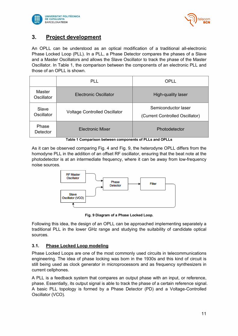
As it can be observed comparing Fig. 4 and Fig. 9, the heterodyne OPLL differs from the homodyne PLL in the addition of an offset RF oscillator, ensuring that the beat note at the photodetector is at an intermediate frequency, where it can be away from low-frequency noise sources.
Fig. 9 Diagram of a Phase Locked Loop.
Following this idea, the design of an OPLL can be approached implementing separately a traditional PLL in the lower GHz range and studying the suitability of candidate optical sources.
3.1. Phase Locked Loop modeling Phase Locked Loops are one of the most commonly used circuits in telecommunications engineering. The idea of phase locking was born in the 1930s and this kind of circuit is still being used as clock generator in microprocessors and as frequency synthesizers in current cellphones.
A PLL is a feedback system that compares an output phase with an input, or reference, phase. Essentially, its output signal is able to track the phase of a certain reference signal. A basic PLL topology is formed by a Phase Detector (PD) and a Voltage-Controlled Oscillator (VCO).
12
The PD is the element that actually performs the phase comparison. It is a circuit whose average output, Vout, is linearly proportional to the phase difference, Δϕ, between its two inputs. In an ideal case, the relationship between Vout and Δϕ is linear and it crosses the origin for Δϕ = 0. The simplest example of a PD is the exclusive OR (XOR). As the phase difference between the pulses varies, so does the width of the output pulses, thereby providing a DC level proportional to Δϕ.
The VCO generates a sinusoidal signal whose instantaneous frequency is controlled by an input voltage. When the output signal of the VCO is skewed by Δt seconds with respect to the reference signal, the PLL tries to align the signal of the VCO with the reference signal. Assuming that the VCO has a single control input, 𝑉NO^_, in order to vary the phase, the frequency must be varied and allow the following integration to take place, where 𝜔R is the Quiescent frequency4 of the VCO and 𝐾`NO denotes the gain, or sensitivity, of the VCO.
𝜙 = a𝜔R + 𝐾`NO𝑉NO^_𝑑𝑡 (11)
This basic topology must be modified for two reasons. The first one is that the signal at the PD output consists of a desirable DC component and undesirable high-frequency components. The second one is that the control signal that runs the oscillator, 𝑉NO^_, must remain in a steady state, which means that it must be filtered. Thus, a Loop Filter (LF) is placed between the PD and the VCO, suppressing the high frequency components and presenting a DC level to the oscillator.
Imagine that at an instant t = t1, the VCO frequency is stepped to a higher value. The circuit starts accumulating phase, decreasing the phase error. When the phase error drops to zero and, if VCONT returns to its original value, the signals remain aligned. The underlying idea is that phase alignment can only be achieved by momentarily changing the frequency of the signal of the VCO.
In every application, the PLL tracks the phase of the reference signal. However, before a PLL can track, it must first reach the phase-locked condition. If the loop is locked, the phase difference ϕOUT – ϕIN is constant. Therefore, it its defined that if the loop is locked, the phase difference is time-invariant. Two important corollaries of this definition are (12) and (13).
𝛿𝜙Od_𝛿𝑡
−𝛿𝜙e^𝛿𝑡
= 0 (12)
𝜔Od_ = 𝜔e^ (13)
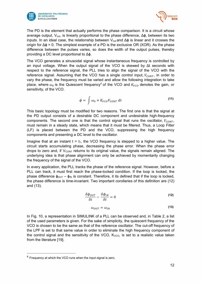
In Fig. 10, a representation in SIMULINK of a PLL can be observed and, in Table 2, a list of the used parameters is given. For the sake of simplicity, the quiescent frequency of the VCO is chosen to be the same as that of the reference oscillator. The cut-off frequency of the LPF is set to that same value in order to eliminate the high frequency component of the control signal and the sensitivity of the VCO, KVCO, is set to a realistic value taken from the literature [19].
4 Frequency at which the VCO runs when the input signal is zero.
13
The behavior of PLLs has both steady state and transient modes of response. When the PLL is locked and nothing changes, the PLL shows a steady state behavior. When the loop undergoes a frequency or phase change, a transient response is observed. However, as long as the changes are small, the PLL recovers and achieves steady state again.
Fig. 10 SIMULINK Schematic of a basic PLL.
PARAMETER VALUE
Quiescent frequency VCO 5 GHz
Reference Oscillator frequency 5 GHz
LPF cut-off frequency 0.5 GHz
KVCO 1.3 GHz Table 2 List of parameters of basic PLL.
3.1.1. Steady state behavior and transient response of Phase Locked Loops In order to perform a study on the steady state of PLLs, it is important to first define the Transfer Function of a basic PLL. From the Laplace Transforms of the elements in Fig. 10, the closed-loop Transfer Function of the PLL is obtained as (15). The transfer function of the PD, the LPF and the VCO (14) is the multiplication of the gains of each element (𝐾EF and𝐾`NO) and the division by 𝑠 that represents the integration of the VCO.
𝑃$(𝑠) =𝐾EF𝐾`NO𝐻#EH(𝑠)
𝑠=𝐾 · 𝐻#EH(𝑠)
𝑠 (14)
𝐻(𝑠) =𝑃$(𝑠)
1 + 𝑃$(𝑠)=
𝐾 · 𝐻#EH(𝑠)𝑠 + 𝐾 · 𝐻#EH(𝑠)
(15)
The LF is configured to be a first order Low Pass Filter (LPF) with one pole at 𝜔#EH and gain 𝐾#EH (16).
𝐻#EH(𝑠) =𝐾#EH
1 + 𝑠𝜔#EH
(16)
The loop is evaluated using the transfer function of the error (17), from which an expression for the steady state error produced by the PLL, 𝜃Q%%j% , is obtained as a function of the phase of the input signal,𝜃kl.
14
𝐻Q(𝑠) =𝜃Q%%j%𝜃kl
=1
1 + 𝑃$(𝑠)=
𝑠𝑠 + 𝐾 · 𝐻#EH(𝑠)
(17)
𝜃Q%%j%(𝑠) = 𝑠 · 𝜃kl(𝑠)
𝑠 + 𝐾 · 𝐻#EH(𝑠) (18)
The error signal is a measure of the phase difference between the reference signal and the output signal of the VCO. Using the Final Value Theorem (FVT), the steady state behavior of a signal is found taking the limit of 𝑠 times its Laplace Transform when s goes to zero (19).
limV→p
𝜃(𝑡) = limq→R
𝑠 · 𝜃(𝑠) (19)
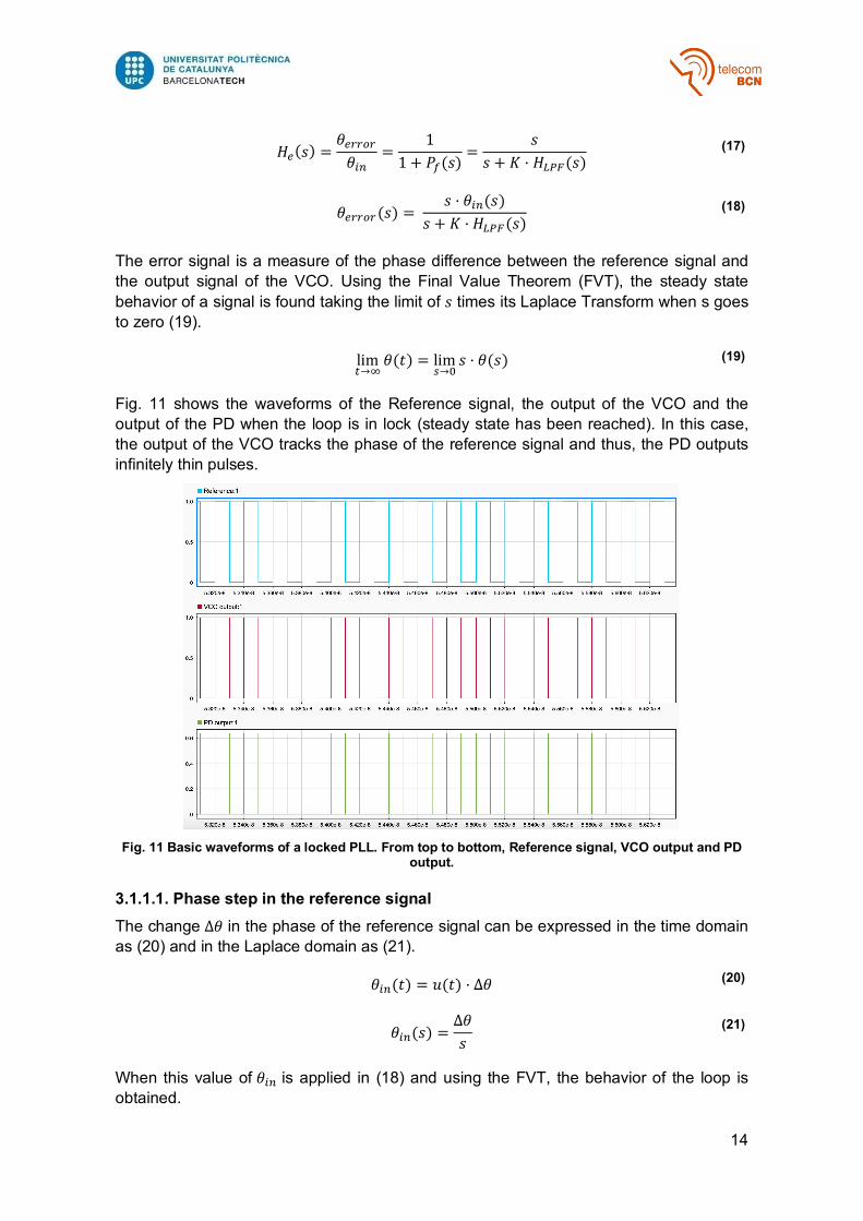
Fig. 11 shows the waveforms of the Reference signal, the output of the VCO and the output of the PD when the loop is in lock (steady state has been reached). In this case, the output of the VCO tracks the phase of the reference signal and thus, the PD outputs infinitely thin pulses.
Fig. 11 Basic waveforms of a locked PLL. From top to bottom, Reference signal, VCO output and PD
output.
3.1.1.1. Phase step in the reference signal The change ∆𝜃 in the phase of the reference signal can be expressed in the time domain as (20) and in the Laplace domain as (21).
𝜃kl(𝑡) = 𝑢(𝑡) · ∆𝜃 (20)
𝜃kl(𝑠) =∆𝜃𝑠
(21)
When this value of 𝜃kl is applied in (18) and using the FVT, the behavior of the loop is obtained.
15
limV→p
𝜃Q%%j%(𝑡) = limq→R
𝑠 ·𝑠 · 𝜃kl(𝑠)
𝑠 + 𝐾 · 𝐻#EH(𝑠)= 𝑠 ·
∆𝜃𝑠 + 𝐾 · 𝐻#EH(𝑠)
= 0 (22)
This result shows that, when the reference signal experiences a phase step, the error signal will, in time, go to zero and the loop will remain in lock.
3.1.1.2. Frequency step in the reference signal Assume that, instead of a phase step, the reference signal undergoes a frequency shift ∆𝜔, which is expressed as (23) and has a Laplace transform as in (24).
𝜔kl(𝑡) = 𝜔R + 𝑢(𝑡) · ∆𝜔 (23)
𝜃kl(𝑠) =∆𝜔𝑠<
(24)
Proceeding as in the previous case, the steady state error due to a phase step is expressed as (25).
limV→p
𝜃Q%%j%(𝑡) = limq→R
𝑠 ·𝑠 · ∆𝜔𝑠<
𝑠 + 𝐾 · 𝐻#EH(𝑠)=
∆𝜔𝐾 · 𝐻#EH(𝑠)
(25)
As it can be observed, in this case, the error is not 0. This means that a steady state error will exist in the output signal, which entails a voltage change in the control signal that drives the VCO.
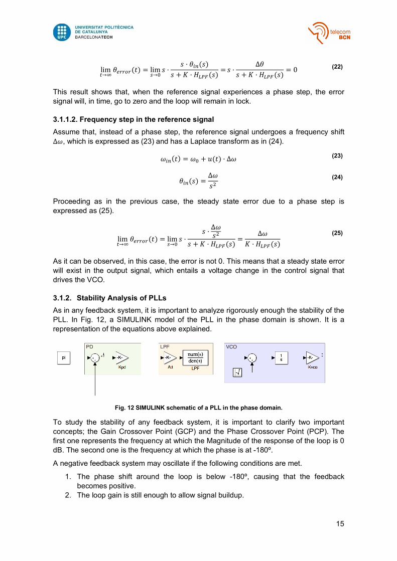
3.1.2. Stability Analysis of PLLs As in any feedback system, it is important to analyze rigorously enough the stability of the PLL. In Fig. 12, a SIMULINK model of the PLL in the phase domain is shown. It is a representation of the equations above explained.
Fig. 12 SIMULINK schematic of a PLL in the phase domain.
To study the stability of any feedback system, it is important to clarify two important concepts; the Gain Crossover Point (GCP) and the Phase Crossover Point (PCP). The first one represents the frequency at which the Magnitude of the response of the loop is 0 dB. The second one is the frequency at which the phase is at -180º.
A negative feedback system may oscillate if the following conditions are met.
1. The phase shift around the loop is below -180º, causing that the feedback becomes positive.
2. The loop gain is still enough to allow signal buildup.
16
The criteria followed in order to control the stability of the loop is to minimize the total phase shift so that for a gain of 0 dB, the phase shift is below -180º. This means that maintaining the GCP below the PCP guarantees the stability of the loop.
Not only the facts that the loop can achieve locking and that it does not oscillate are important. Two of the most relevant performance metrics of PLLs are the Hold-in range and the Acquisition range.
The Hold-in range, also known as Lock range, is defined as the largest change in the free-running frequency of the SL over which the loop still remains in lock. In other words, it is the frequency range around the free running frequency that the loop can track.
The Acquisition range, also known as Capture range, is the range of input frequencies around the VCO center frequency onto which the loop will lock from an unlocked condition.
These metrics, along with the analysis of the stability of the loop, are detailed in Section 4.
3.2. Optical source analysis A natural candidate for the role of an optical VCO, or rather a Current Controlled Oscillator, is the semiconductor laser (SCL) due to the sensitivity of the frequency of the SCL to injection current. Equation (26) relates the frequency shift of an SCL, ∆𝜔U, to the changes in the internal optical energy density. 𝛼 is the phase-amplitude coupling factor, 𝑃(𝑡) is the photon density, 𝑃R is the average photon density, 𝜖 is the gain suppression factor, and 𝜏: is the photon lifetime at transparency of the semiconductor gain medium.
∆𝜔U(𝑡) = −
𝛼2w1𝑃R𝜕(∆𝑃)𝜕𝑡
+𝜖𝜏:Δ𝑃(𝑡)y (26)
However, 𝑃(𝑡) is not a directly controlled physical variable. Such a variable would be 𝑖U(𝑡), the injection current. Lengthy derivations such as those in [30] show that at frequencies considerably below that of the modulation resonance of the SCL, the photon density is proportional to the current input above the threshold 𝑖U,VW (27). In (28), 𝑉{ is the mode volume and Γ} is the fill factor, approximately the ratio of the active volume to the modal volume, and 𝑒 is the electron charge.
𝑃(𝑡) = 𝑔[𝑖U(𝑡) − 𝑖U,VW] (27)
𝑔 =
Γ}𝜏:𝑒𝑉{
(28)
Using (27), a relation between the frequency shift, ∆𝜔U, and the injection current can be obtained.
∆𝜔U(𝑡) = −
𝛼2w
1,𝑖UR−𝑖U,VW1
𝜕(∆𝑖U)𝜕𝑡
+𝜖𝑔𝜏:Δ𝑖Uy = 𝑎
𝜕𝜕𝑡∆𝑖U + 𝑏∆𝑖U (29)
Considering that ∆𝜔U can be understood as the time derivative of the phase, an expression that demonstrates that the phase can be adjusted by controlling the injection current is obtained (31).
17
∆𝜔U(𝑡) =
𝜕∆𝜙$�𝜕𝑡
(30)
Δ𝜙U = 𝑎 · 𝑖U(𝑡) + 𝑏a 𝑖U(𝑡)𝑑𝑡
V
R (31)
Nevertheless, when using a Distributed Feedback laser (DFB) as the SL, two important issues arise that need to be addressed. The first one is that, despite only a Phase Modulation component is desired, it is observed that also a residual Amplitude Modulation (AM) component is obtained. The second is that there is a thermal contribution to the Frequency Modulation5 in lower frequencies that cannot be ignored.
3.2.1. Thermal and electronic contributions to the Frequency Modulation Most monoelectrode DFB lasers suffer from a dip in their FM response due to the conflict between opposite thermal and electronic effects. The thermal FM response is only found at low frequencies, while electronic, or carrier induced, FM response is flat from DC level to the surroundings of the relaxation frequency of the laser. To compute the total FM response, both effects must be studied separately.
Let us start with the thermal FM response. From [31], the Fourier Transform of the heat equation together with the appropriate boundary conditions leads to (32), where 𝜐 is the normalized modulation frequency, 𝑓 is the modulation frequency, 𝑓[ is the thermal cutoff frequency, 𝜅 the thermal diffusivity and 𝐾G is the thermal resistance of the laser. 𝑄(𝜐) is the heat generated in the laser and it is proportional to the injection current.
𝑇(𝜐) =𝐾G𝑄(𝜐)2�𝑗𝜐
w𝑡𝑎𝑛ℎ,�𝑗𝜐1+ 𝑡𝑎𝑛ℎ ��𝑗𝜐2�y (32)
𝜐 = 𝑓𝑓[;𝑓[ =
𝜅2𝜋𝑙<
(33)
Taking into account that the optical frequency of the laser, 𝑓j:V, depends on the length of the cavity,𝐿, and the effective index6, 𝑛Q, of the propagating mode, 𝑝, according to (34), the thermal contribution to the FM response, 𝐻VW, is obtained combining (32) and the logarithmic derivative of (34).
𝑓j:V =𝑝 · 𝑐2𝑛Q𝐿
(34)
𝐻VW(𝜐) = −
𝑓j:V𝐾G𝐾�(𝛼^ + 𝛼#)2
·tanh,�𝑗𝜐1 + tanh�
�𝑗𝜐2 �
�𝑗𝜐= −𝐾VW · ℎVW(𝜐)
(35)
5 It is important to remember that Phase and Frequency modulation are, mathematically speaking, identical twins. The only difference is that one corresponds to a modulation pattern that is the differential of that produced by the other. 6 These two quantities also depend on the temperature and, in the end, on the injection current.
18
Regarding the electronic response, at low frequencies, the carrier-induced FM response can be considered constant.
𝐻QU(𝜐) = 𝐾QU (36)
The total FM response is obtained by simply adding the thermal and electronic contributions.
𝐻}(𝜐) = 𝐻VW(𝜐) + 𝐻QU(𝜐) = 𝐾QU − 𝐾VW · ℎVW(𝜐) = 𝐾VW · [𝑎 − ℎVW(𝜐)] (37)
𝑎 = 𝐾QU𝐾VW
(38)
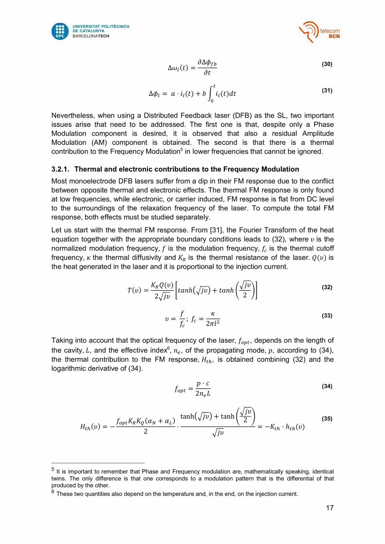
Fig. 13 shows that a dip associated to a phase reversal in the impulse response of the FM is clearly observed. A thermal cutoff frequency of 50 KHz is used for three different values of a. Typically, this dip is 2-3 dB deep.
Fig. 13 Magnitude and phase of the FM response. From [31].
3.2.2. Presence of undesired Amplitude Modulation component As it has already been stated, the goal is to control the phase of the signal using the injection current and it has already been established how this is carried out. Nevertheless, when studying available DFBs, it is observed that there is a residual AM component.
Assume the laser is modulated using an AC perturbation of the form (39). The laser will be modulated in phase and amplitude, as in (40), being 𝐵 the amplitude modulation depth and 𝐶 the phase modulation depth. They represent the product between the amplitude of the AC perturbation, 𝐴{, and the response of the laser to amplitude (𝐾�) and phase (𝐾[) modulation.
𝑚(𝑡) = 𝐴{cos(𝜔GH𝑡 + 𝜙GH) (39)
𝐸� =𝐴�,1 + 𝐵 · 𝑐𝑜𝑠(𝜔GH𝑡 + 𝜙GH)1𝑒�,��V����N·[jq(���V����)1 (40)
19
𝐸< = 𝐴<𝑒�,(��±� )V1 (41)
The field 𝐸�, coming from the modulated DFB, and the field 𝐸<, coming from the reference laser are combined into a photodiode of responsivity 𝑅 that provides an output current as (42). This complex expression is divided according to the component that causes each part; (42.a) shows the DC component of the signal, where 𝛼 represents the attenuation term of a DC block, (42.b) is the Baseband AM, (42.c) comes from the beat signal carrier and (42.d) characterizes the carrier AM.
𝐼EF = 𝑅 · 𝐼j:V = 𝑅 · |𝐸� + 𝐸<|< = (42)
𝛼𝑅 w|𝐴�|< �1 +𝐵<
2� + |𝐴<|<y + (42.a)
𝑅 w|𝐴�|< ¤𝐵<
2cos(2(𝜔GH𝑡 + 2𝜙GH) + 2𝐵𝑐𝑜𝑠(𝜔GH𝑡 + 𝜙GH)¥y + (42.b)
𝑅¦2𝐴�𝐴<𝑐𝑜𝑠,𝜔�𝑡 + 𝜙R + 𝐶 · 𝑐𝑜𝑠(𝜔GH𝑡 + 𝜙GH)1§ + (42.c)
𝑅¦2𝐴�𝐴<𝐵𝑐𝑜𝑠(𝜔GH𝑡 + 𝜙GH)𝑐𝑜𝑠,𝜔�𝑡 + 𝜙R + 𝐶 · 𝑐𝑜𝑠(𝜔GH𝑡 + 𝜙GH)1§ (42.d)
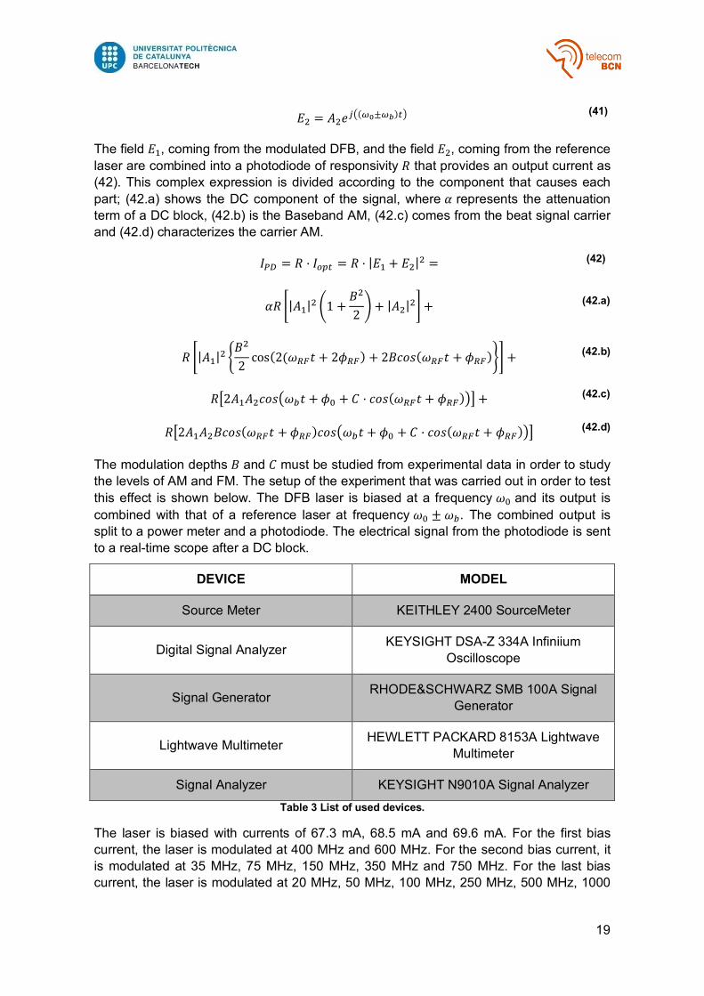
The modulation depths 𝐵 and 𝐶 must be studied from experimental data in order to study the levels of AM and FM. The setup of the experiment that was carried out in order to test this effect is shown below. The DFB laser is biased at a frequency 𝜔R and its output is combined with that of a reference laser at frequency 𝜔R ± 𝜔�. The combined output is split to a power meter and a photodiode. The electrical signal from the photodiode is sent to a real-time scope after a DC block.
DEVICE MODEL
Source Meter KEITHLEY 2400 SourceMeter
Digital Signal Analyzer KEYSIGHT DSA-Z 334A Infiniium Oscilloscope
Signal Generator RHODE&SCHWARZ SMB 100A Signal Generator
Lightwave Multimeter HEWLETT PACKARD 8153A Lightwave Multimeter
Signal Analyzer KEYSIGHT N9010A Signal Analyzer Table 3 List of used devices.
The laser is biased with currents of 67.3 mA, 68.5 mA and 69.6 mA. For the first bias current, the laser is modulated at 400 MHz and 600 MHz. For the second bias current, it is modulated at 35 MHz, 75 MHz, 150 MHz, 350 MHz and 750 MHz. For the last bias current, the laser is modulated at 20 MHz, 50 MHz, 100 MHz, 250 MHz, 500 MHz, 1000
20
MHz. Each modulation frequency, 𝜔GH , is tested with modulation amplitudes, 𝐴{ , between 0.5 and 7.5 mA.
Fig. 14 Setup used to measure the response of the DFB.
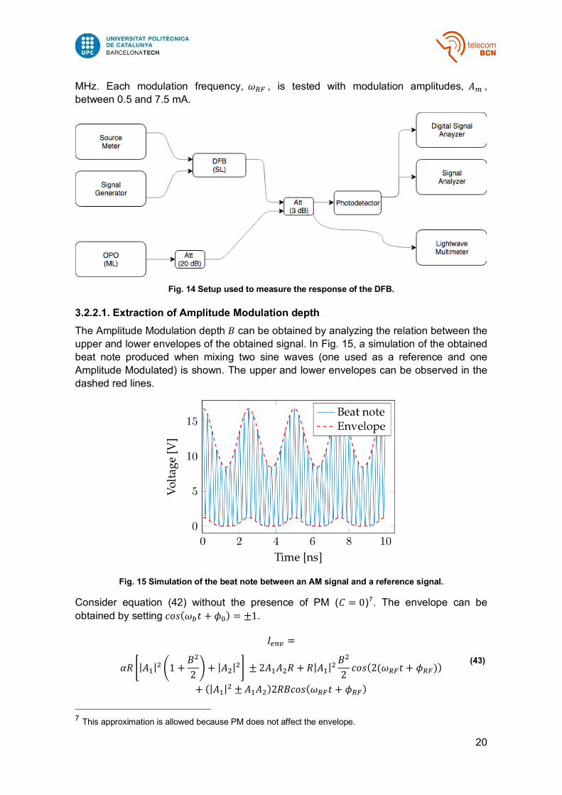
3.2.2.1. Extraction of Amplitude Modulation depth The Amplitude Modulation depth 𝐵 can be obtained by analyzing the relation between the upper and lower envelopes of the obtained signal. In Fig. 15, a simulation of the obtained beat note produced when mixing two sine waves (one used as a reference and one Amplitude Modulated) is shown. The upper and lower envelopes can be observed in the dashed red lines.
Fig. 15 Simulation of the beat note between an AM signal and a reference signal.
Consider equation (42) without the presence of PM (𝐶 = 0)7. The envelope can be obtained by setting 𝑐𝑜𝑠(𝜔�𝑡 + 𝜙R) = ±1.
𝐼Ql¨ =
𝛼𝑅 w|𝐴�|< �1 +𝐵<
2� + |𝐴<|<y ± 2𝐴�𝐴<𝑅 + 𝑅|𝐴�|<
𝐵<
2𝑐𝑜𝑠(2(𝜔GH𝑡 + 𝜙GH))
+ (|𝐴�|< ± 𝐴�𝐴<)2𝑅𝐵𝑐𝑜𝑠(𝜔GH𝑡 + 𝜙GH)
(43)
7 This approximation is allowed because PM does not affect the envelope.
21
It is necessary to find the zeros of the first and second derivative of 𝐼Ql¨ . These occur
when 𝑠𝑖𝑛(𝜔GH𝑡 + 𝜙GH) = 0 and when 𝑐𝑜𝑠(𝜔GH𝑡 + 𝜙GH) =�±©ª©«¬
. The modulation depth can be calculated in each of the envelopes as it follows.
Δ𝐼Ql¨ = 𝐼Ql¨|���VR − 𝐼Ql¨|���V® (44)
Δ𝐼Ql¨¯: = 4𝑅𝐵𝐴�[𝐴� + 𝐴<]
(45)
Δ𝐼Ql¨Uj± = 4𝑅𝐵𝐴�[𝐴� − 𝐴<] (46)
The difference between the modulation depth in the upper and lower envelopes is now used to extract the parameter 𝐵.
Δ𝐼Ql¨¯: − Δ𝐼Ql¨Uj± = 2 · 4𝑅𝐴�𝐴< · 𝐵 (47)
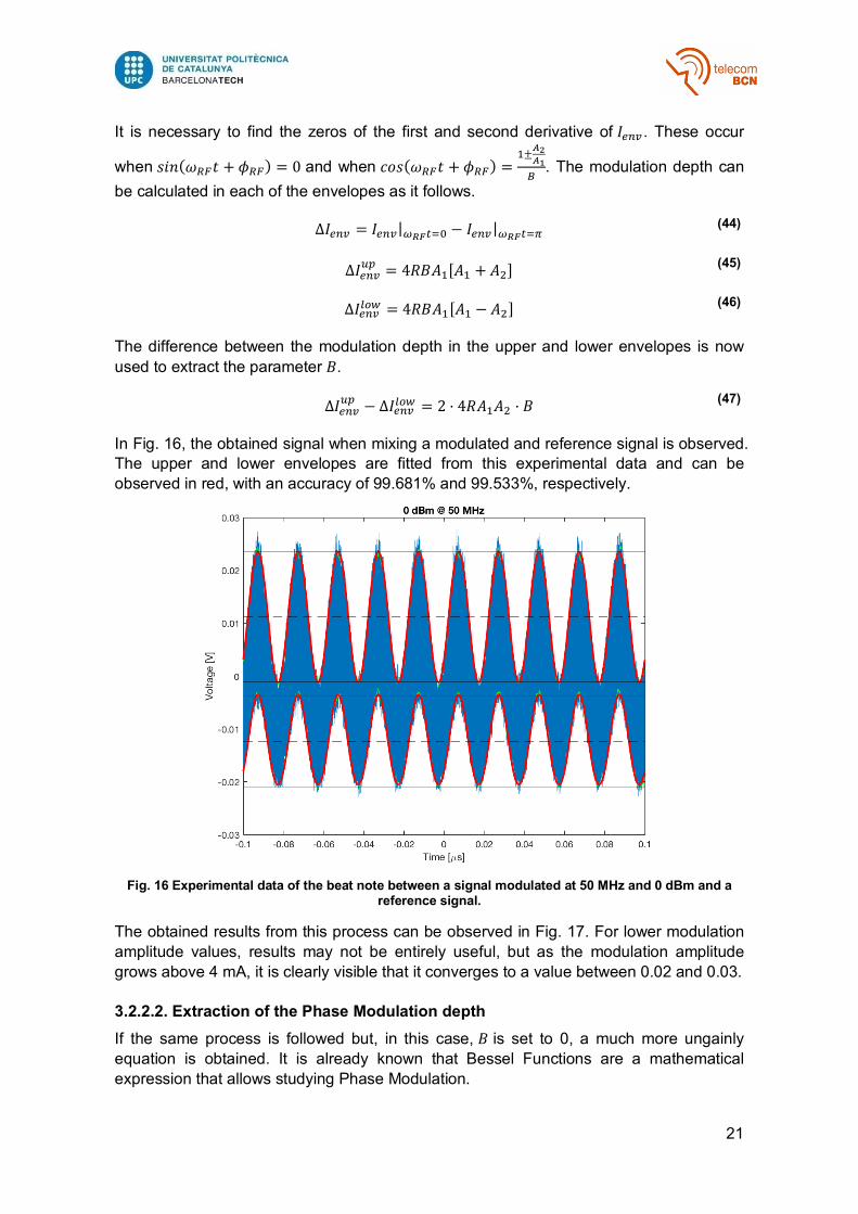
In Fig. 16, the obtained signal when mixing a modulated and reference signal is observed. The upper and lower envelopes are fitted from this experimental data and can be observed in red, with an accuracy of 99.681% and 99.533%, respectively.
Fig. 16 Experimental data of the beat note between a signal modulated at 50 MHz and 0 dBm and a
reference signal.
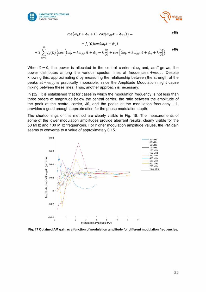
The obtained results from this process can be observed in Fig. 17. For lower modulation amplitude values, results may not be entirely useful, but as the modulation amplitude grows above 4 mA, it is clearly visible that it converges to a value between 0.02 and 0.03.
3.2.2.2. Extraction of the Phase Modulation depth If the same process is followed but, in this case, 𝐵 is set to 0, a much more ungainly equation is obtained. It is already known that Bessel Functions are a mathematical expression that allows studying Phase Modulation.
22
𝑐𝑜𝑠,𝜔�𝑡 + 𝜙R + 𝐶 · 𝑐𝑜𝑠(𝜔GH𝑡 + 𝜙GH)1 = (48)
= 𝐽R(𝐶)𝑐𝑜𝑠(𝜔�𝑡 + 𝜙R)
+ 2³𝐽´(𝐶) µ𝑐𝑜𝑠 ¶(𝜔� − 𝑘𝜔GH)𝑡 + 𝜙R − 𝑘𝜋2¸ + 𝑐𝑜𝑠 ¶(𝜔� + 𝑘𝜔GH)𝑡 + 𝜙R + 𝑘
𝜋2¸¹
p
´�
(49)
When 𝐶 = 0, the power is allocated in the central carrier at 𝜔� and, as 𝐶 grows, the power distributes among the various spectral lines at frequencies ±𝑛𝜔GH . Despite knowing this, approximating 𝐶 by measuring the relationship between the strength of the peaks at ±𝑛𝜔GH is practically impossible, since the Amplitude Modulation might cause mixing between these lines. Thus, another approach is necessary.
In [32], it is established that for cases in which the modulation frequency is not less than three orders of magnitude below the central carrier, the ratio between the amplitude of the peak at the central carrier, J0, and the peaks at the modulation frequency, J1, provides a good enough approximation for the phase modulation depth.
The shortcomings of this method are clearly visible in Fig. 18. The measurements of some of the lower modulation amplitudes provide aberrant results, clearly visible for the 50 MHz and 100 MHz frequencies. For higher modulation amplitude values, the PM gain seems to converge to a value of approximately 0.15.
Fig. 17 Obtained AM gain as a function of modulation amplitude for different modulation frequencies.
23
Fig. 18 Obtained PM gain as a function of modulation amplitude for different modulation frequencies.
In spite of the fact of not being able to clearly extract values for the AM and PM depths, it can be observed that the AM produces an undesired distortion in the signal. This reflects the need for some other type of modulator.
3.2.3. Hybrid III-V/Si MOS modulators A possible approach in order to mitigate the aforementioned AM component is the integration of a DFB and an Electro-Absorption Modulator (EAM), as in [33]. This does not only increase the fabrication complexity, but it also adds a critical point in the generation of a modulated signal; the synchronization between the signals modulating the DFB and the EAM. In an effort to keep the system with a complexity as low as possible, hybrid III-V/Si phase modulators are studied.
This type of modulators is the evolution of Silicon optical modulators that rely on pn junctions [34], pin junctions [35] and MOS junctions [36][37] to obtain optical phase modulation. This PM is obtained using the free-carrier plasma dispersion effect through modulation of the carrier density. Among them, carrier accumulation in a MOS junction consisting of a poly-crystalline-Silicon/SiO2/Silicon stack exhibits the highest PM efficiency with a voltage-length product (𝑉𝜋𝐿) of 0.2 V·cm and a modulation bandwidth of 40 Gbps.
However, reducing this value even more has become quite a challenge using only Silicon modulators. Reducing the gate oxide thickness is the most usual approach but, as it is thinned, the MOS capacitance grows, degrading the modulation bandwidth. The most promising solution is the heterogeneous integration of III-V materials onto Silicon.
III-V materials are chemical compounds with at least one element from group III from the periodic table and one element from group V. Indium phosphide (InP) based materials provide a large electron-induced refractive index change due to the large carrier plasma effect and band filling effect. In addition, the higher electron mobility contributes to
24
reducing carrier plasma absorption loss and the resistance-capacitance (RC) time delay. Introducing an n-type III-V material into a MOS capacitor enables a high overlap integral between the optical intensity and carrier distribution in both the n-type III-V material and the p-type Silicon8. In [28] and [29], optical modulators with InGaAsP/Si hybrid MOS phase shifters are investigated. These devices use the carrier-induced changes in the refractive index of both InGaAsP and Silicon to change the effective index of the propagating mode and, thus, change the phase of the signal (50).
∆𝜙 =2𝜋𝜆Δ𝑛Q$$𝐿 (50)
To obtain the effective index change, Δ𝑛Q$$, it is important to first analyze the change in the refractive index of the p-type Silicon and the n-type InGaAsP. From the Plasma-Drude model [38], the unperturbed index plus the change in the index can be calculated from overall carrier density as (51), where N and P are the carrier densities, 𝜀{ is the permittivity of the unperturbed material, 𝑚Q
∗ and 𝑚W∗ are the effective masses of electrons
and holes, respectively.
𝑛 + 𝑖𝑘 =½𝜀{ − 𝑒
<
𝜔 ¾ 𝑁𝑚Q∗𝜔 + 𝑖 𝑒µQ
+ 𝑃𝑚W∗𝜔 + 𝑖 𝑒µW
Á
𝜀R
(51)
An expansion from the above model at a particular wavelength, 𝜆, assuming complex refractive indices can be calculated from the change in the carrier density for most semiconductors as (52), where 𝑒 is the electronic charge, 𝜀R is the permittivity of free space, 𝑛 is the index of the unperturbed material, 𝑚[Q
∗ and 𝑚[W∗ are the conductivity
effective masses of electrons and holes and ∆𝑁Q and ∆𝑁W are the changes in electron and hole densities.
∆𝑛 = −�
𝑒<𝜆<
8𝜋<𝑐<𝜀R𝑛� w∆𝑁Q𝑚[Q∗ +
∆𝑁W𝑚[W∗ y
(52)
Nevertheless, these expressions are not sufficient to model the real refractive index change that Silicon and InGaAsP undergo. In practice, when calculating this change for the Silicon, at a wavelength of 1550 nm, it is common to employ empirical equations (53), as explained in [39].
𝑛"k = −,8.8 · 10ÄÅ𝑁Q + 8.5𝑁WR.Ç1 · 10Ä�Ç (53)
Regarding the InGaAsP, (52) only takes into account the plasma effect (free-carrier absorption). However, in [40], it is proven that Bandfilling and Band-gap shrinkage effects must also be taken into account. The equations that model these new effects are obtained after a quite problematic mathematical procedure but, fitting the data from [28], an approximation can be obtained. 8 An extrinsic semiconductor refers to a semiconductor material that has been doped, i.e. a doping agent has been introduced. In the case of a p-type semiconductor, the hole concentration is increased and holes become the majority carriers. In an n-type semiconductor, the electron concentration is increased and they become the majority carriers.
25
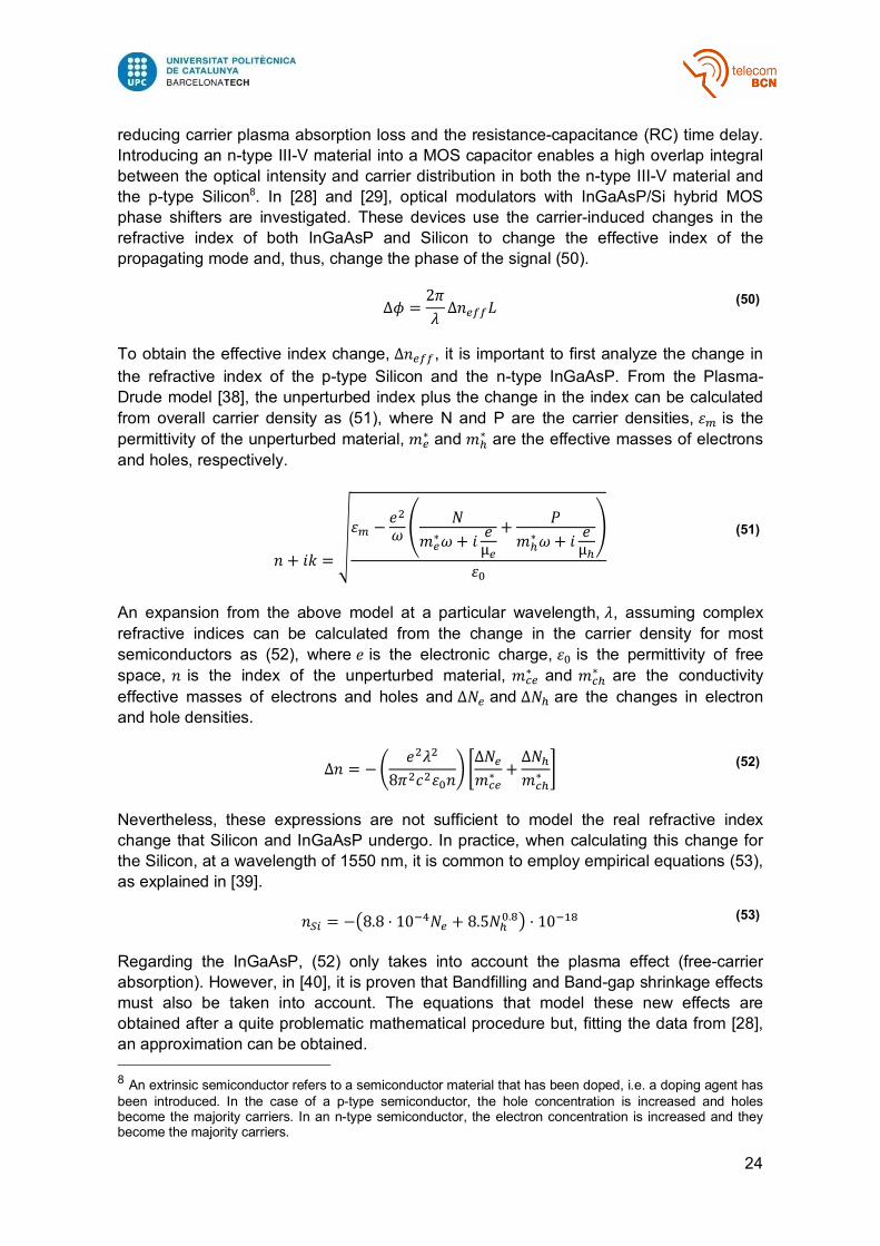
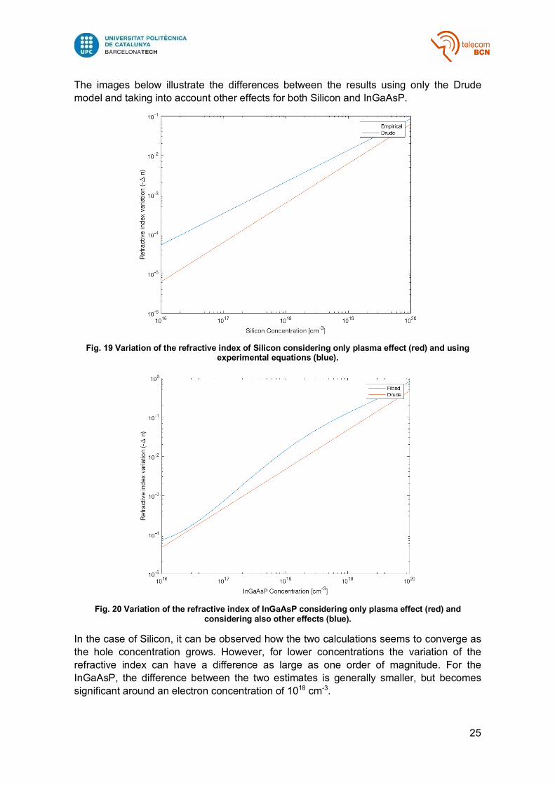
The images below illustrate the differences between the results using only the Drude model and taking into account other effects for both Silicon and InGaAsP.
Fig. 19 Variation of the refractive index of Silicon considering only plasma effect (red) and using
experimental equations (blue).
Fig. 20 Variation of the refractive index of InGaAsP considering only plasma effect (red) and
considering also other effects (blue).
In the case of Silicon, it can be observed how the two calculations seems to converge as the hole concentration grows. However, for lower concentrations the variation of the refractive index can have a difference as large as one order of magnitude. For the InGaAsP, the difference between the two estimates is generally smaller, but becomes significant around an electron concentration of 1018 cm-3.
26
It is important to notice that the variations of the refractive index are shown in their absolute value since, actually, as the carrier concentration grows, the refractive index of the material becomes smaller.
The experiments from [28] and [29] are used as a reference to create a model that assesses the suitability of the laser structure described in Section 2 to act as a phase modulator. This model works in three different software tools. The main workflow is to calculate the change in the carrier concentration with Lumerical’s DEVICE, use the information provided to calculate how this carrier concentration change alters the refractive index, as shown in Fig. 19 and Fig. 20, of the Silicon and the III-V material with MATLAB and calculate the effective index change with Lumerical’s MODE.
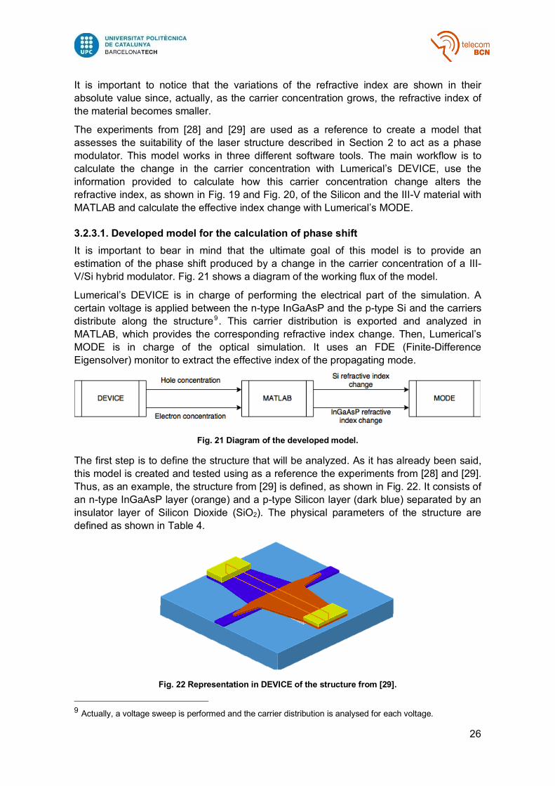
3.2.3.1. Developed model for the calculation of phase shift It is important to bear in mind that the ultimate goal of this model is to provide an estimation of the phase shift produced by a change in the carrier concentration of a III-V/Si hybrid modulator. Fig. 21 shows a diagram of the working flux of the model.
Lumerical’s DEVICE is in charge of performing the electrical part of the simulation. A certain voltage is applied between the n-type InGaAsP and the p-type Si and the carriers distribute along the structure9. This carrier distribution is exported and analyzed in MATLAB, which provides the corresponding refractive index change. Then, Lumerical’s MODE is in charge of the optical simulation. It uses an FDE (Finite-Difference Eigensolver) monitor to extract the effective index of the propagating mode.
Fig. 21 Diagram of the developed model.
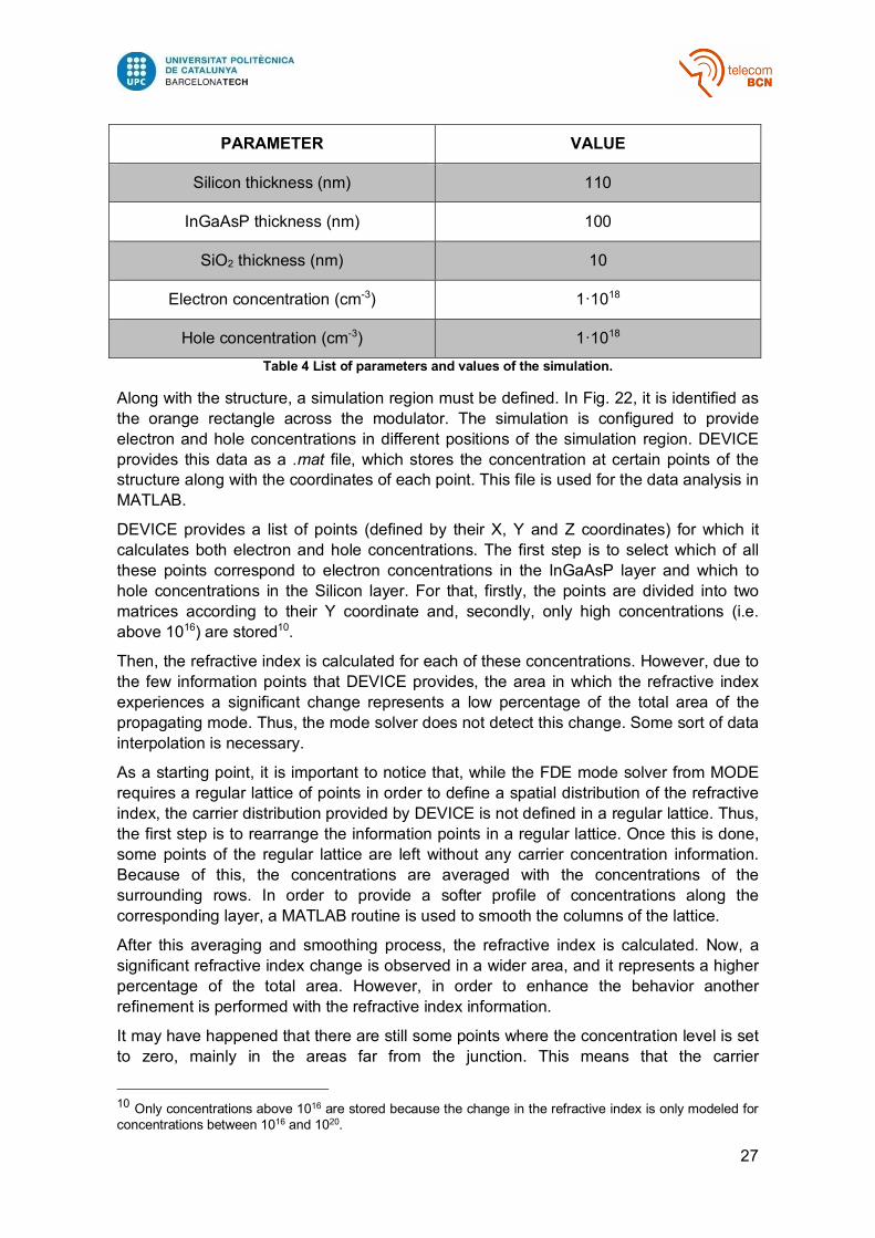
The first step is to define the structure that will be analyzed. As it has already been said, this model is created and tested using as a reference the experiments from [28] and [29]. Thus, as an example, the structure from [29] is defined, as shown in Fig. 22. It consists of an n-type InGaAsP layer (orange) and a p-type Silicon layer (dark blue) separated by an insulator layer of Silicon Dioxide (SiO2). The physical parameters of the structure are defined as shown in Table 4.
Fig. 22 Representation in DEVICE of the structure from [29].
9 Actually, a voltage sweep is performed and the carrier distribution is analysed for each voltage.
27
PARAMETER VALUE
Silicon thickness (nm) 110
InGaAsP thickness (nm) 100
SiO2 thickness (nm) 10
Electron concentration (cm-3) 1·1018
Hole concentration (cm-3) 1·1018
Table 4 List of parameters and values of the simulation.
Along with the structure, a simulation region must be defined. In Fig. 22, it is identified as the orange rectangle across the modulator. The simulation is configured to provide electron and hole concentrations in different positions of the simulation region. DEVICE provides this data as a .mat file, which stores the concentration at certain points of the structure along with the coordinates of each point. This file is used for the data analysis in MATLAB.
DEVICE provides a list of points (defined by their X, Y and Z coordinates) for which it calculates both electron and hole concentrations. The first step is to select which of all these points correspond to electron concentrations in the InGaAsP layer and which to hole concentrations in the Silicon layer. For that, firstly, the points are divided into two matrices according to their Y coordinate and, secondly, only high concentrations (i.e. above 1016) are stored10.
Then, the refractive index is calculated for each of these concentrations. However, due to the few information points that DEVICE provides, the area in which the refractive index experiences a significant change represents a low percentage of the total area of the propagating mode. Thus, the mode solver does not detect this change. Some sort of data interpolation is necessary.
As a starting point, it is important to notice that, while the FDE mode solver from MODE requires a regular lattice of points in order to define a spatial distribution of the refractive index, the carrier distribution provided by DEVICE is not defined in a regular lattice. Thus, the first step is to rearrange the information points in a regular lattice. Once this is done, some points of the regular lattice are left without any carrier concentration information. Because of this, the concentrations are averaged with the concentrations of the surrounding rows. In order to provide a softer profile of concentrations along the corresponding layer, a MATLAB routine is used to smooth the columns of the lattice.
After this averaging and smoothing process, the refractive index is calculated. Now, a significant refractive index change is observed in a wider area, and it represents a higher percentage of the total area. However, in order to enhance the behavior another refinement is performed with the refractive index information.
It may have happened that there are still some points where the concentration level is set to zero, mainly in the areas far from the junction. This means that the carrier
10 Only concentrations above 1016 are stored because the change in the refractive index is only modeled for concentrations between 1016 and 1020.
28
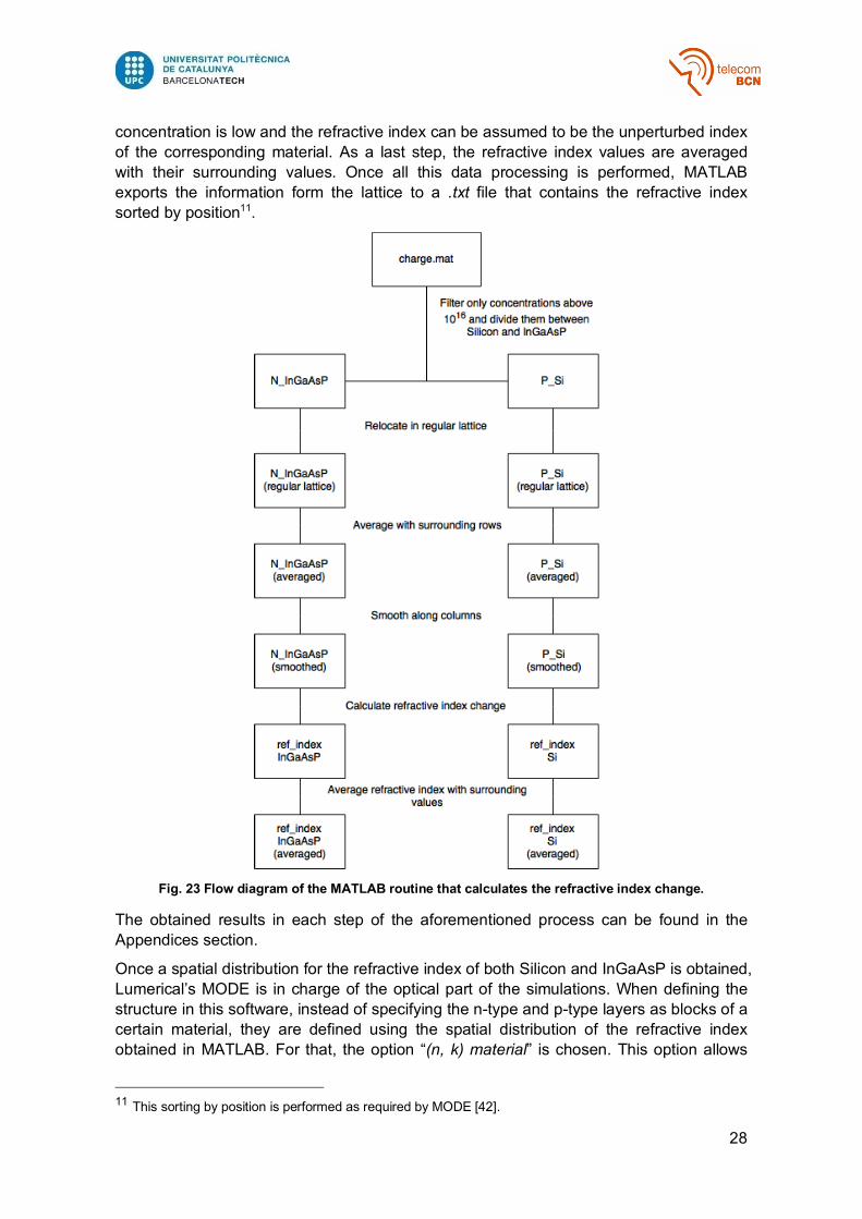
concentration is low and the refractive index can be assumed to be the unperturbed index of the corresponding material. As a last step, the refractive index values are averaged with their surrounding values. Once all this data processing is performed, MATLAB exports the information form the lattice to a .txt file that contains the refractive index sorted by position11.
Fig. 23 Flow diagram of the MATLAB routine that calculates the refractive index change.
The obtained results in each step of the aforementioned process can be found in the Appendices section.
Once a spatial distribution for the refractive index of both Silicon and InGaAsP is obtained, Lumerical’s MODE is in charge of the optical part of the simulations. When defining the structure in this software, instead of specifying the n-type and p-type layers as blocks of a certain material, they are defined using the spatial distribution of the refractive index obtained in MATLAB. For that, the option “(n, k) material” is chosen. This option allows
11 This sorting by position is performed as required by MODE [42].
29
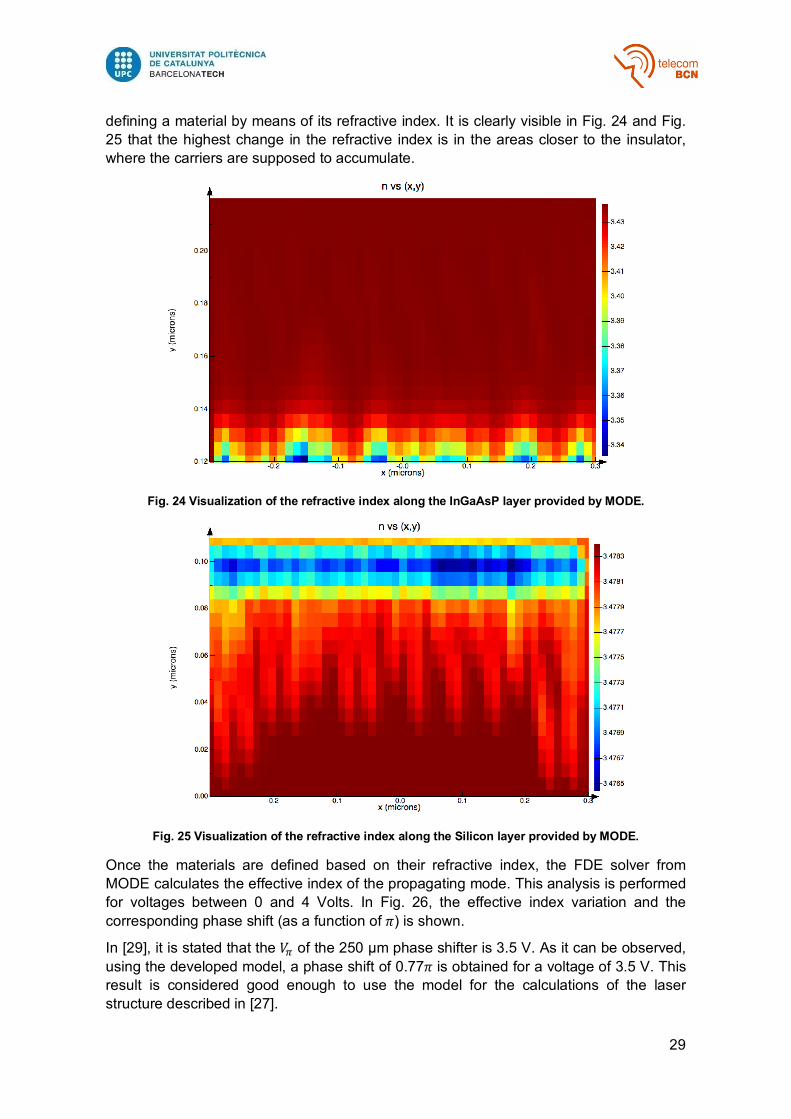
defining a material by means of its refractive index. It is clearly visible in Fig. 24 and Fig. 25 that the highest change in the refractive index is in the areas closer to the insulator, where the carriers are supposed to accumulate.
Fig. 24 Visualization of the refractive index along the InGaAsP layer provided by MODE.
Fig. 25 Visualization of the refractive index along the Silicon layer provided by MODE.
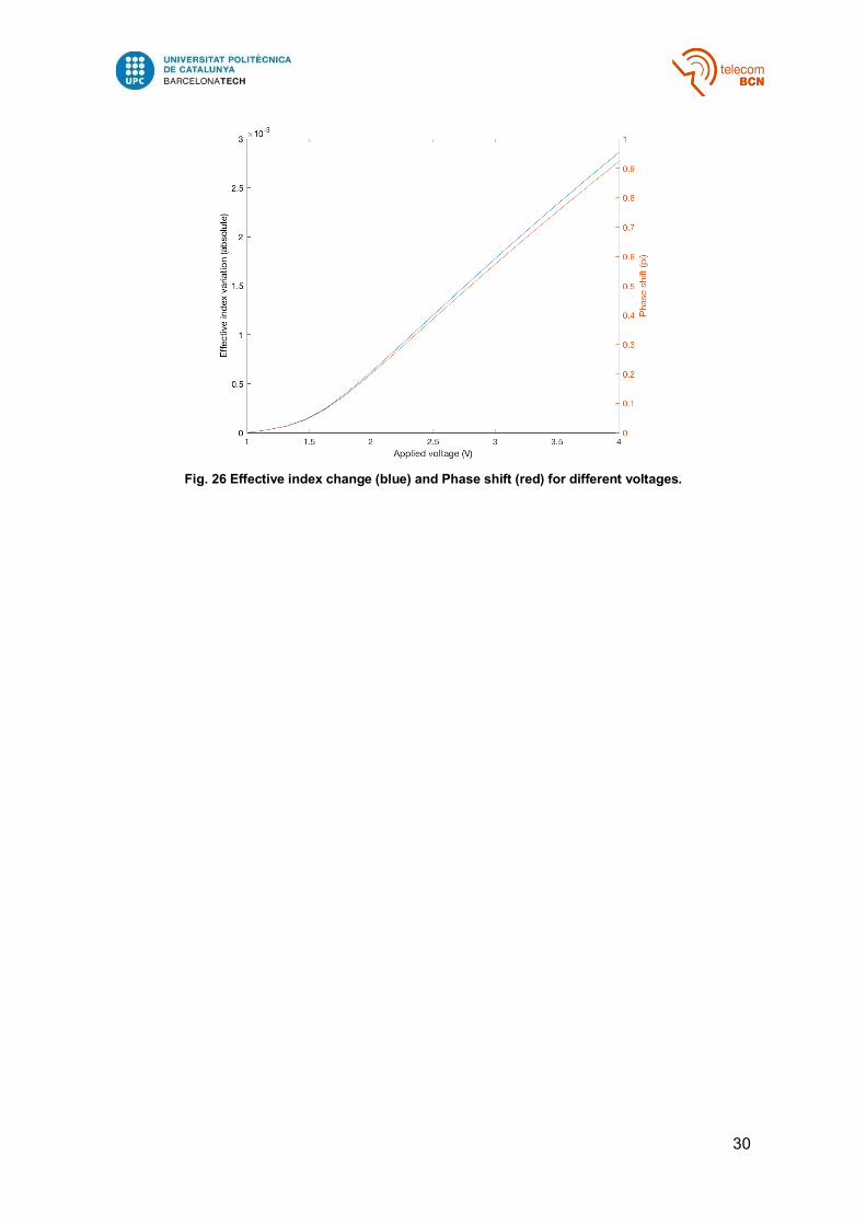
Once the materials are defined based on their refractive index, the FDE solver from MODE calculates the effective index of the propagating mode. This analysis is performed for voltages between 0 and 4 Volts. In Fig. 26, the effective index variation and the corresponding phase shift (as a function of 𝜋) is shown.
In [29], it is stated that the 𝑉® of the 250 µm phase shifter is 3.5 V. As it can be observed, using the developed model, a phase shift of 0.77𝜋 is obtained for a voltage of 3.5 V. This result is considered good enough to use the model for the calculations of the laser structure described in [27].
30
Fig. 26 Effective index change (blue) and Phase shift (red) for different voltages.
31
4. Results
As it has already been explained, the design and analysis of an OPLL can be divided into electrical and optical domains. First, an analysis of the all-electrical PLL is performed. Its behavior is analyzed and its shortcomings are exposed. Also, a stability analysis is presented.
Regarding the optical part of the device, the laser structure proposed in [27] is analyzed as a Phase Modulator with the model explained in the previous section.
To evaluate the results of the different experiments, it is important to have in mind the goal of the device. The purpose of the OPLL is that the SL locks to the ML, i.e. tracks the frequency and phase of the ML, with a certain offset frequency. The ML is assumed to be a frequency comb, which means that its spectrum consists of a series of discrete, equally spaced frequency lines. These lines may cover a range of several GHz and the goal is that the SL may try to lock to any of them, which means that an Acquisition range of several GHz is desired. That is the main criterion that drives the analysis.
4.1. Basic PLL analysis In Section 3, the basic structure of a PLL and its waveforms are shown in Fig. 10 and Fig. 11, respectively. However, it is important to perform a more thorough analysis taking into account other performance metrics, such as the Hold-in and Acquisition ranges.
As it was already shown, when the quiescent frequency of the VCO is the same as the frequency of the reference oscillator, the loop easily achieves locking. But, when the aforementioned performance metrics are tested, the faults in this device become apparent.
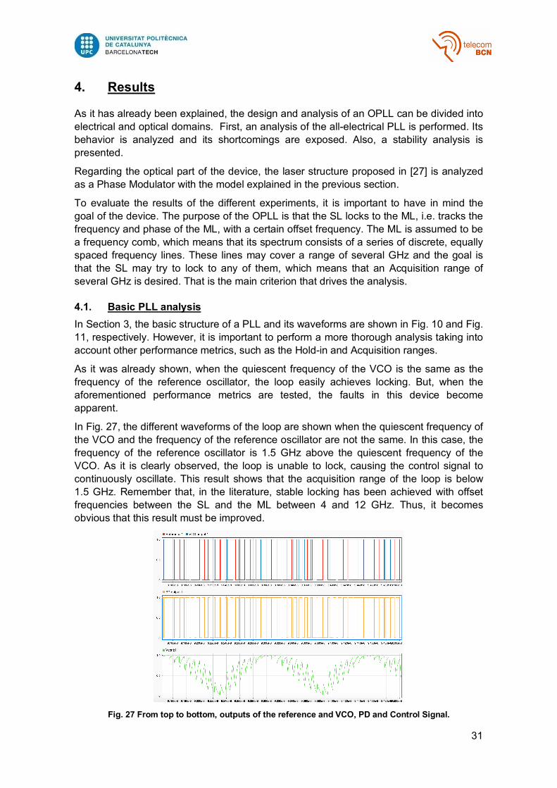
In Fig. 27, the different waveforms of the loop are shown when the quiescent frequency of the VCO and the frequency of the reference oscillator are not the same. In this case, the frequency of the reference oscillator is 1.5 GHz above the quiescent frequency of the VCO. As it is clearly observed, the loop is unable to lock, causing the control signal to continuously oscillate. This result shows that the acquisition range of the loop is below 1.5 GHz. Remember that, in the literature, stable locking has been achieved with offset frequencies between the SL and the ML between 4 and 12 GHz. Thus, it becomes obvious that this result must be improved.
Fig. 27 From top to bottom, outputs of the reference and VCO, PD and Control Signal.
32
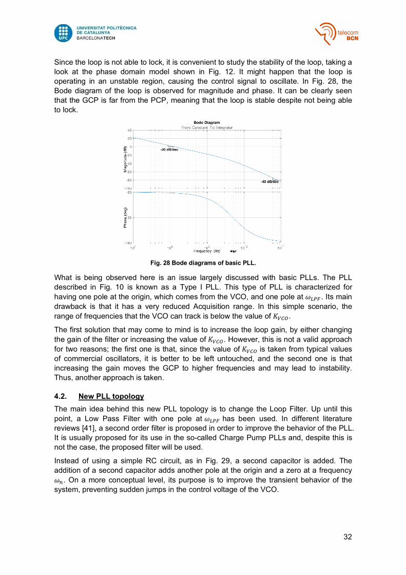
Since the loop is not able to lock, it is convenient to study the stability of the loop, taking a look at the phase domain model shown in Fig. 12. It might happen that the loop is operating in an unstable region, causing the control signal to oscillate. In Fig. 28, the Bode diagram of the loop is observed for magnitude and phase. It can be clearly seen that the GCP is far from the PCP, meaning that the loop is stable despite not being able to lock.
Fig. 28 Bode diagrams of basic PLL.
What is being observed here is an issue largely discussed with basic PLLs. The PLL described in Fig. 10 is known as a Type I PLL. This type of PLL is characterized for having one pole at the origin, which comes from the VCO, and one pole at 𝜔#EH . Its main drawback is that it has a very reduced Acquisition range. In this simple scenario, the range of frequencies that the VCO can track is below the value of 𝐾`NO.
The first solution that may come to mind is to increase the loop gain, by either changing the gain of the filter or increasing the value of 𝐾`NO. However, this is not a valid approach for two reasons; the first one is that, since the value of 𝐾`NO is taken from typical values of commercial oscillators, it is better to be left untouched, and the second one is that increasing the gain moves the GCP to higher frequencies and may lead to instability. Thus, another approach is taken.
4.2. New PLL topology The main idea behind this new PLL topology is to change the Loop Filter. Up until this point, a Low Pass Filter with one pole at 𝜔#EH has been used. In different literature reviews [41], a second order filter is proposed in order to improve the behavior of the PLL. It is usually proposed for its use in the so-called Charge Pump PLLs and, despite this is not the case, the proposed filter will be used.
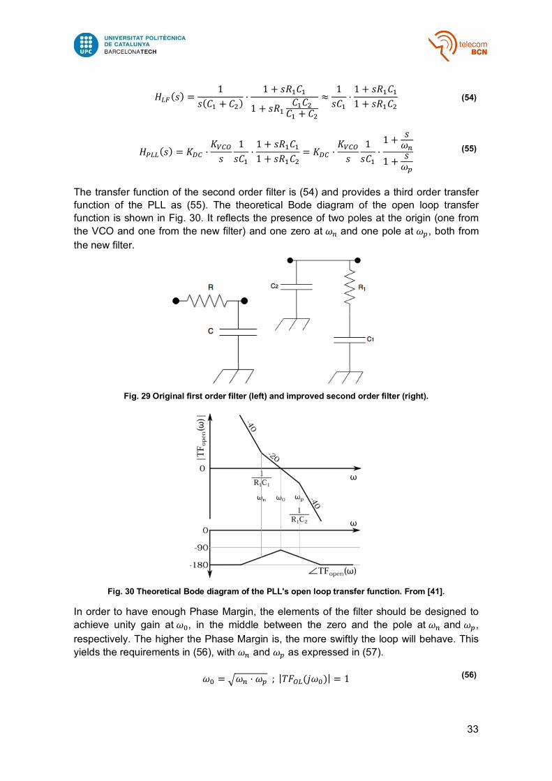
Instead of using a simple RC circuit, as in Fig. 29, a second capacitor is added. The addition of a second capacitor adds another pole at the origin and a zero at a frequency 𝜔l. On a more conceptual level, its purpose is to improve the transient behavior of the system, preventing sudden jumps in the control voltage of the VCO.
33
𝐻#H(𝑠) =1
𝑠(𝐶� + 𝐶<)·
1 + 𝑠𝑅�𝐶�
1 + 𝑠𝑅�𝐶�𝐶<𝐶� + 𝐶<
≈1𝑠𝐶�
·1 + 𝑠𝑅�𝐶�1 + 𝑠𝑅�𝐶<
(54)
𝐻E##(𝑠) = 𝐾FN ·𝐾`NO𝑠
1𝑠𝐶�
·1 + 𝑠𝑅�𝐶�1 + 𝑠𝑅�𝐶<
= 𝐾FN ·𝐾`NO𝑠
1𝑠𝐶�
·1 + 𝑠
𝜔l1 + 𝑠
𝜔: (55)
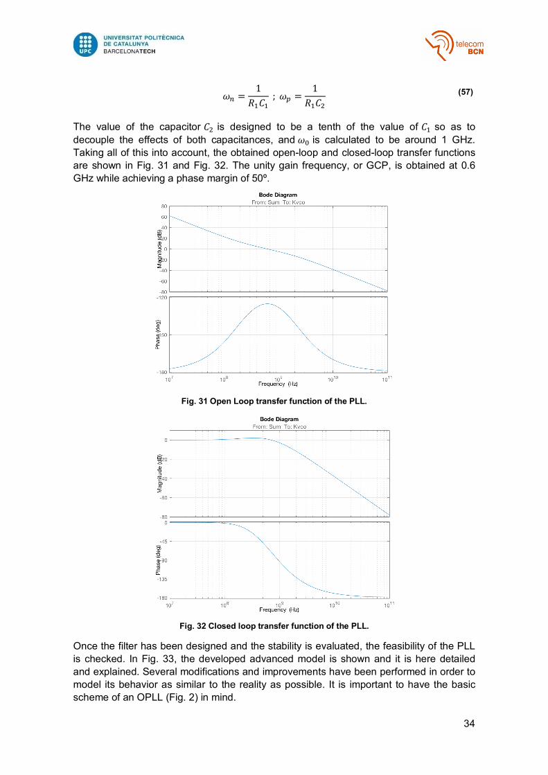
The transfer function of the second order filter is (54) and provides a third order transfer function of the PLL as (55). The theoretical Bode diagram of the open loop transfer function is shown in Fig. 30. It reflects the presence of two poles at the origin (one from the VCO and one from the new filter) and one zero at 𝜔l and one pole at 𝜔:, both from the new filter.
Fig. 29 Original first order filter (left) and improved second order filter (right).
Fig. 30 Theoretical Bode diagram of the PLL's open loop transfer function. From [41].
In order to have enough Phase Margin, the elements of the filter should be designed to achieve unity gain at 𝜔R, in the middle between the zero and the pole at 𝜔l and 𝜔:, respectively. The higher the Phase Margin is, the more swiftly the loop will behave. This yields the requirements in (56), with 𝜔l and 𝜔: as expressed in (57).
𝜔R = �𝜔l · 𝜔:; |𝑇𝐹O#(𝑗𝜔R)| = 1 (56)
34
𝜔l =1
𝑅�𝐶�; 𝜔: =
1𝑅�𝐶<
(57)
The value of the capacitor 𝐶< is designed to be a tenth of the value of 𝐶� so as to decouple the effects of both capacitances, and 𝜔R is calculated to be around 1 GHz. Taking all of this into account, the obtained open-loop and closed-loop transfer functions are shown in Fig. 31 and Fig. 32. The unity gain frequency, or GCP, is obtained at 0.6 GHz while achieving a phase margin of 50º.
Fig. 31 Open Loop transfer function of the PLL.
Fig. 32 Closed loop transfer function of the PLL.
Once the filter has been designed and the stability is evaluated, the feasibility of the PLL is checked. In Fig. 33, the developed advanced model is shown and it is here detailed and explained. Several modifications and improvements have been performed in order to model its behavior as similar to the reality as possible. It is important to have the basic scheme of an OPLL (Fig. 2) in mind.
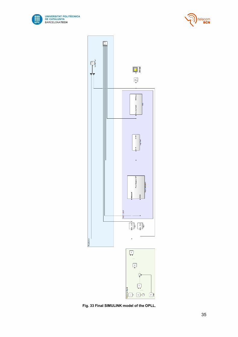
35
Fig. 33 Final SIMULINK model of the OPLL.
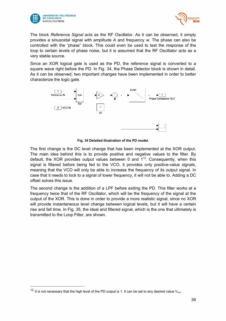
36
The block Reference Signal acts as the RF Oscillator. As it can be observed, it simply provides a sinusoidal signal with amplitude A and frequency w. The phase can also be controlled with the “phase” block. This could even be used to test the response of the loop to certain levels of phase noise, but it is assumed that the RF Oscillator acts as a very stable source.
Since an XOR logical gate is used as the PD, the reference signal is converted to a square wave right before the PD. In Fig. 34, the Phase Detector block is shown in detail. As it can be observed, two important changes have been implemented in order to better characterize the logic gate.
Fig. 34 Detailed illustration of the PD model.
The first change is the DC level change that has been implemented at the XOR output. The main idea behind this is to provide positive and negative values to the filter. By default, the XOR provides output values between 0 and 112. Consequently, when this signal is filtered before being fed to the VCO, it provides only positive-value signals, meaning that the VCO will only be able to increase the frequency of its output signal. In case that it needs to lock to a signal of lower frequency, it will not be able to. Adding a DC offset solves this issue.
The second change is the addition of a LPF before exiting the PD. This filter works at a frequency twice that of the RF Oscillator, which will be the frequency of the signal at the output of the XOR. This is done in order to provide a more realistic signal, since no XOR will provide instantaneous level change between logical levels, but it will have a certain rise and fall time. In Fig. 35, the ideal and filtered signal, which is the one that ultimately is transmitted to the Loop Filter, are shown.
12 It is not necessary that the high level of the PD output is 1. It can be set to any desired value Vout.
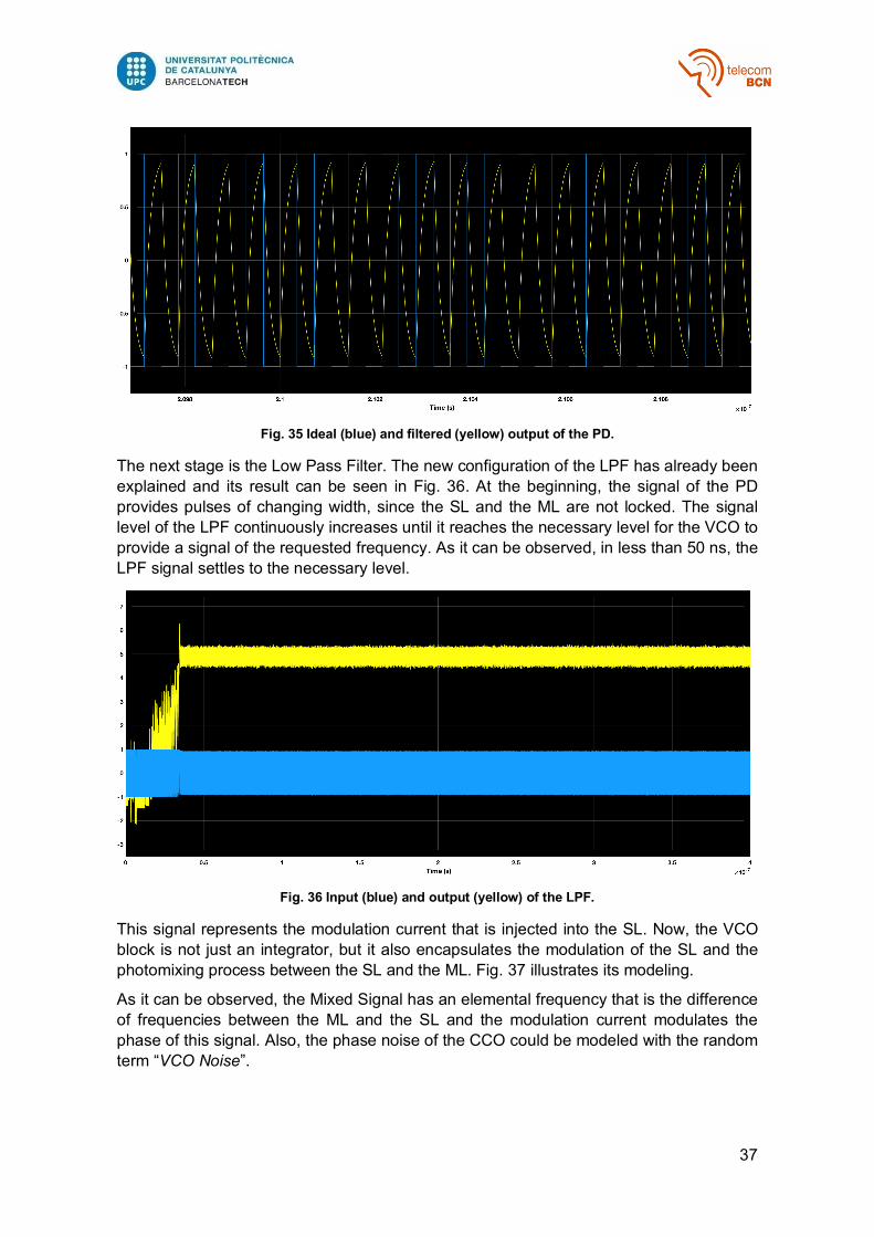
37
Fig. 35 Ideal (blue) and filtered (yellow) output of the PD.
The next stage is the Low Pass Filter. The new configuration of the LPF has already been explained and its result can be seen in Fig. 36. At the beginning, the signal of the PD provides pulses of changing width, since the SL and the ML are not locked. The signal level of the LPF continuously increases until it reaches the necessary level for the VCO to provide a signal of the requested frequency. As it can be observed, in less than 50 ns, the LPF signal settles to the necessary level.
Fig. 36 Input (blue) and output (yellow) of the LPF.
This signal represents the modulation current that is injected into the SL. Now, the VCO block is not just an integrator, but it also encapsulates the modulation of the SL and the photomixing process between the SL and the ML. Fig. 37 illustrates its modeling.
As it can be observed, the Mixed Signal has an elemental frequency that is the difference of frequencies between the ML and the SL and the modulation current modulates the phase of this signal. Also, the phase noise of the CCO could be modeled with the random term “VCO Noise”.
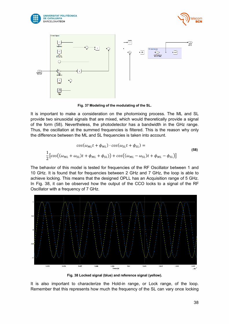
38
Fig. 37 Modeling of the modulating of the SL.
It is important to make a consideration on the photomixing process. The ML and SL provide two sinusoidal signals that are mixed, which would theoretically provide a signal of the form (58). Nevertheless, the photodetector has a bandwidth in the GHz range. Thus, the oscillation at the summed frequencies is filtered. This is the reason why only the difference between the ML and SL frequencies is taken into account.
𝑐𝑜𝑠(𝜔2#𝑡 + 𝜙2#) · 𝑐𝑜𝑠(𝜔"#𝑡 + 𝜙"#) =
12¦𝑐𝑜𝑠,(𝜔2# + 𝜔"#)𝑡 + 𝜙2# + 𝜙"#)1 + 𝑐𝑜𝑠,(𝜔2# − 𝜔"#)𝑡 + 𝜙2# − 𝜙"#1§
(58)
The behavior of this model is tested for frequencies of the RF Oscillator between 1 and 10 GHz. It is found that for frequencies between 2 GHz and 7 GHz, the loop is able to achieve locking. This means that the designed OPLL has an Acquisition range of 5 GHz. In Fig. 38, it can be observed how the output of the CCO locks to a signal of the RF Oscillator with a frequency of 7 GHz.
Fig. 38 Locked signal (blue) and reference signal (yellow).
It is also important to characterize the Hold-in range, or Lock range, of the loop. Remember that this represents how much the frequency of the SL can vary once locking
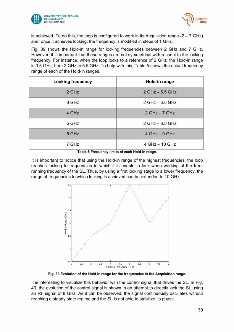
39
is achieved. To do this, the loop is configured to work in its Acquisition range (2 – 7 GHz) and, once it achieves locking, the frequency is modified in steps of 1 GHz.
Fig. 39 shows the Hold-in range for locking frequencies between 2 GHz and 7 GHz. However, it is important that these ranges are not symmetrical with respect to the locking frequency. For instance, when the loop locks to a reference of 2 GHz, the Hold-in range is 3.5 GHz, from 2 GHz to 5.5 GHz. To help with this, Table 5 shows the actual frequency range of each of the Hold-in ranges.
Locking frequency Hold-in range
2 GHz 2 GHz – 5.5 GHz
3 GHz 2 GHz – 6.5 GHz
4 GHz 2 GHz – 7 GHz
5 GHz 2 GHz – 8.5 GHz
6 GHz 4 GHz – 9 GHz
7 GHz 4 GHz – 10 GHz Table 5 Frequency limits of each Hold-in range.
It is important to notice that using the Hold-in range of the highest frequencies, the loop reaches locking to frequencies to which it is unable to lock when working at the free-running frequency of the SL. Thus, by using a first locking stage to a lower frequency, the range of frequencies to which locking is achieved can be extended to 10 GHz.
Fig. 39 Evolution of the Hold-in range for the frequencies in the Acquisition range.
It is interesting to visualize this behavior with the control signal that drives the SL. In Fig. 40, the evolution of the control signal is shown in an attempt to directly lock the SL using an RF signal of 8 GHz. As it can be observed, the signal continuously oscillates without reaching a steady state regime and the SL is not able to stabilize its phase.
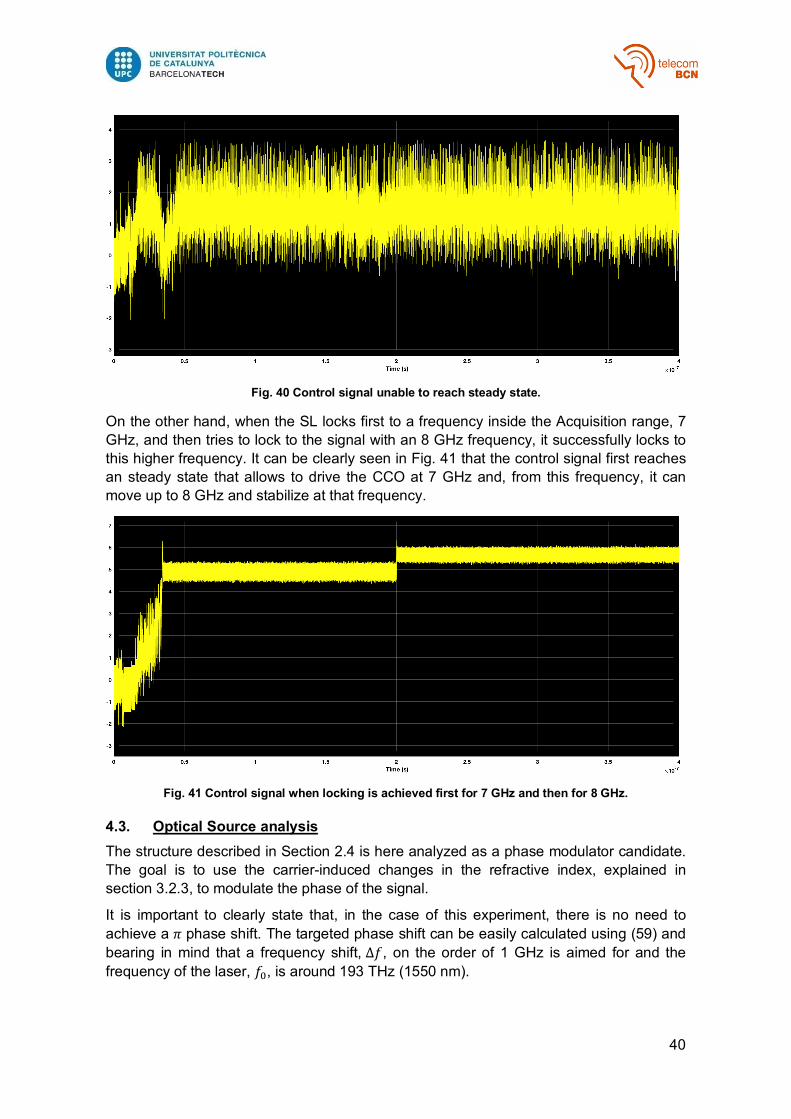
40
Fig. 40 Control signal unable to reach steady state.
On the other hand, when the SL locks first to a frequency inside the Acquisition range, 7 GHz, and then tries to lock to the signal with an 8 GHz frequency, it successfully locks to this higher frequency. It can be clearly seen in Fig. 41 that the control signal first reaches an steady state that allows to drive the CCO at 7 GHz and, from this frequency, it can move up to 8 GHz and stabilize at that frequency.
Fig. 41 Control signal when locking is achieved first for 7 GHz and then for 8 GHz.
4.3. Optical Source analysis The structure described in Section 2.4 is here analyzed as a phase modulator candidate. The goal is to use the carrier-induced changes in the refractive index, explained in section 3.2.3, to modulate the phase of the signal.
It is important to clearly state that, in the case of this experiment, there is no need to achieve a 𝜋 phase shift. The targeted phase shift can be easily calculated using (59) and bearing in mind that a frequency shift, ∆𝑓, on the order of 1 GHz is aimed for and the frequency of the laser, 𝑓R, is around 193 THz (1550 nm).
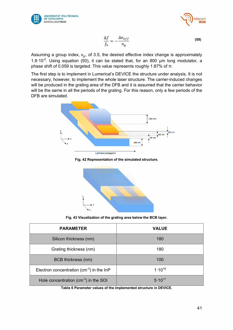
41
∆𝑓𝑓R= −
∆𝑛Q$$𝑛�
(59)
Assuming a group index, 𝑛�, of 3.5, the desired effective index change is approximately 1.8·10-5. Using equation (50), it can be stated that, for an 800 µm long modulator, a phase shift of 0.059 is targeted. This value represents roughly 1.87% of π.
The first step is to implement in Lumerical’s DEVICE the structure under analysis. It is not necessary, however, to implement the whole laser structure. The carrier-induced changes will be produced in the grating area of the DFB and it is assumed that the carrier behavior will be the same in all the periods of the grating. For this reason, only a few periods of the DFB are simulated.
Fig. 42 Representation of the simulated structure.
Fig. 43 Visualization of the grating area below the BCB layer.
PARAMETER VALUE
Silicon thickness (nm) 180
Grating thickness (nm) 180
BCB thickness (nm) 100
Electron concentration (cm-3) in the InP 1·1018
Hole concentration (cm-3) in the SOI 5·1017
Table 6 Parameter values of the implemented structure in DEVICE.
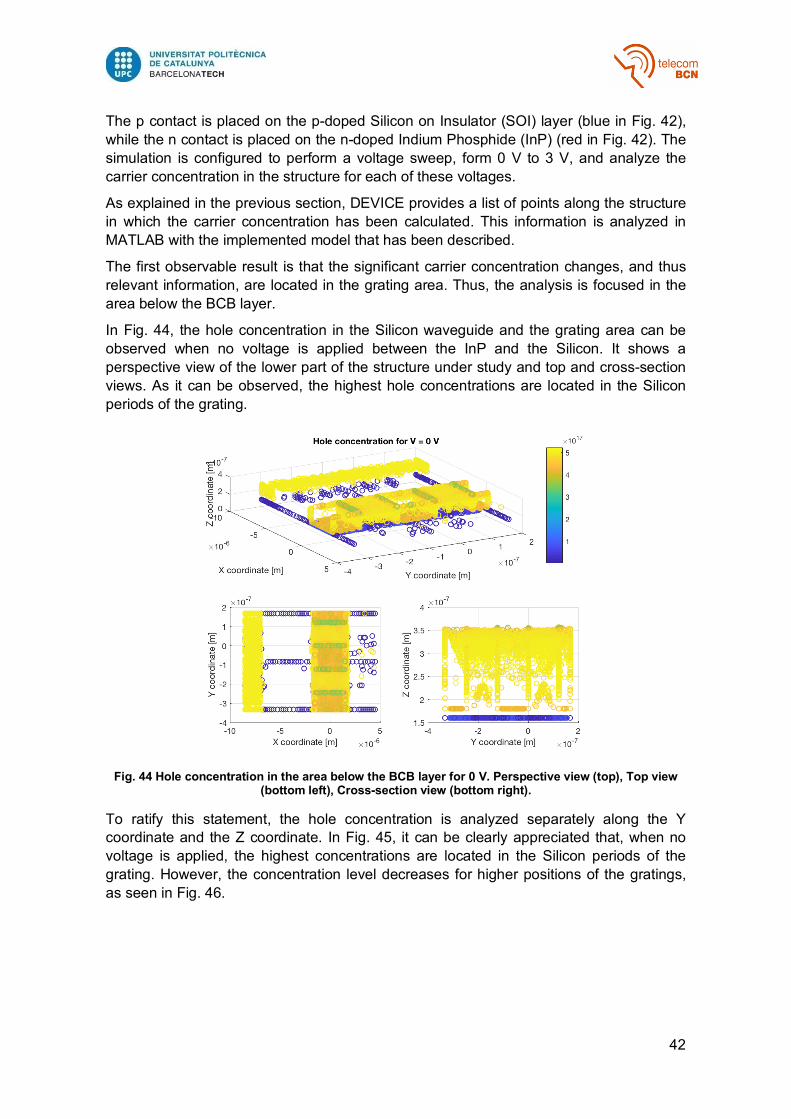
42
The p contact is placed on the p-doped Silicon on Insulator (SOI) layer (blue in Fig. 42), while the n contact is placed on the n-doped Indium Phosphide (InP) (red in Fig. 42). The simulation is configured to perform a voltage sweep, form 0 V to 3 V, and analyze the carrier concentration in the structure for each of these voltages.
As explained in the previous section, DEVICE provides a list of points along the structure in which the carrier concentration has been calculated. This information is analyzed in MATLAB with the implemented model that has been described.
The first observable result is that the significant carrier concentration changes, and thus relevant information, are located in the grating area. Thus, the analysis is focused in the area below the BCB layer.
In Fig. 44, the hole concentration in the Silicon waveguide and the grating area can be observed when no voltage is applied between the InP and the Silicon. It shows a perspective view of the lower part of the structure under study and top and cross-section views. As it can be observed, the highest hole concentrations are located in the Silicon periods of the grating.
Fig. 44 Hole concentration in the area below the BCB layer for 0 V. Perspective view (top), Top view
(bottom left), Cross-section view (bottom right).
To ratify this statement, the hole concentration is analyzed separately along the Y coordinate and the Z coordinate. In Fig. 45, it can be clearly appreciated that, when no voltage is applied, the highest concentrations are located in the Silicon periods of the grating. However, the concentration level decreases for higher positions of the gratings, as seen in Fig. 46.
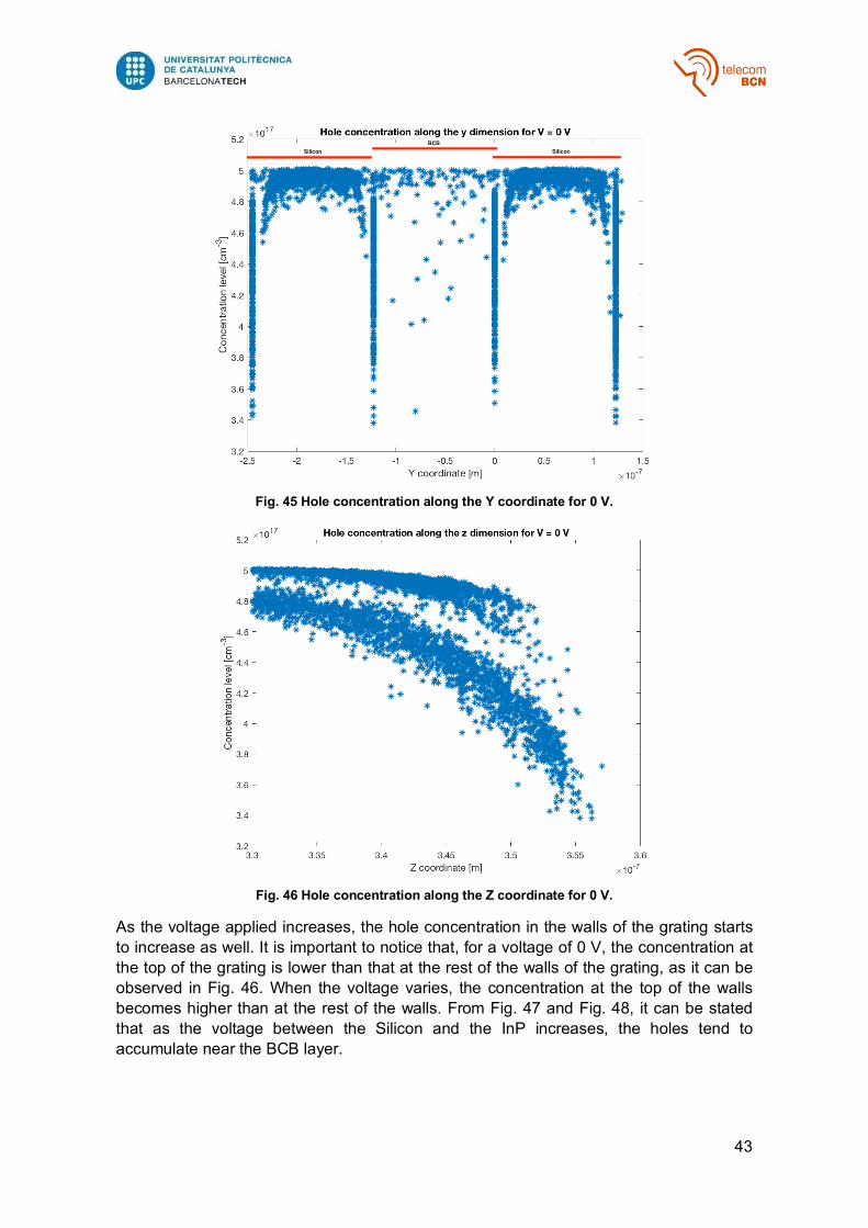
43
Fig. 45 Hole concentration along the Y coordinate for 0 V.
Fig. 46 Hole concentration along the Z coordinate for 0 V.
As the voltage applied increases, the hole concentration in the walls of the grating starts to increase as well. It is important to notice that, for a voltage of 0 V, the concentration at the top of the grating is lower than that at the rest of the walls of the grating, as it can be observed in Fig. 46. When the voltage varies, the concentration at the top of the walls becomes higher than at the rest of the walls. From Fig. 47 and Fig. 48, it can be stated that as the voltage between the Silicon and the InP increases, the holes tend to accumulate near the BCB layer.
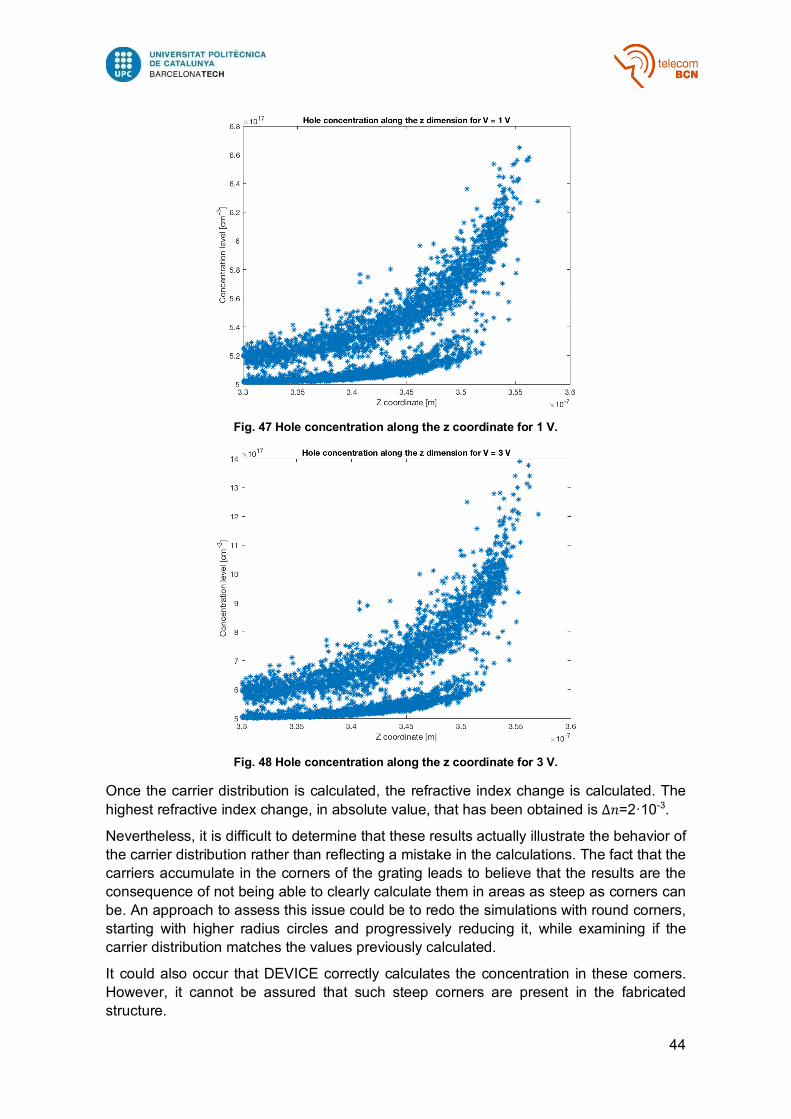
44
Fig. 47 Hole concentration along the z coordinate for 1 V.
Fig. 48 Hole concentration along the z coordinate for 3 V.
Once the carrier distribution is calculated, the refractive index change is calculated. The highest refractive index change, in absolute value, that has been obtained is ∆𝑛=2·10-3.
Nevertheless, it is difficult to determine that these results actually illustrate the behavior of the carrier distribution rather than reflecting a mistake in the calculations. The fact that the carriers accumulate in the corners of the grating leads to believe that the results are the consequence of not being able to clearly calculate them in areas as steep as corners can be. An approach to assess this issue could be to redo the simulations with round corners, starting with higher radius circles and progressively reducing it, while examining if the carrier distribution matches the values previously calculated.
It could also occur that DEVICE correctly calculates the concentration in these corners. However, it cannot be assured that such steep corners are present in the fabricated structure.
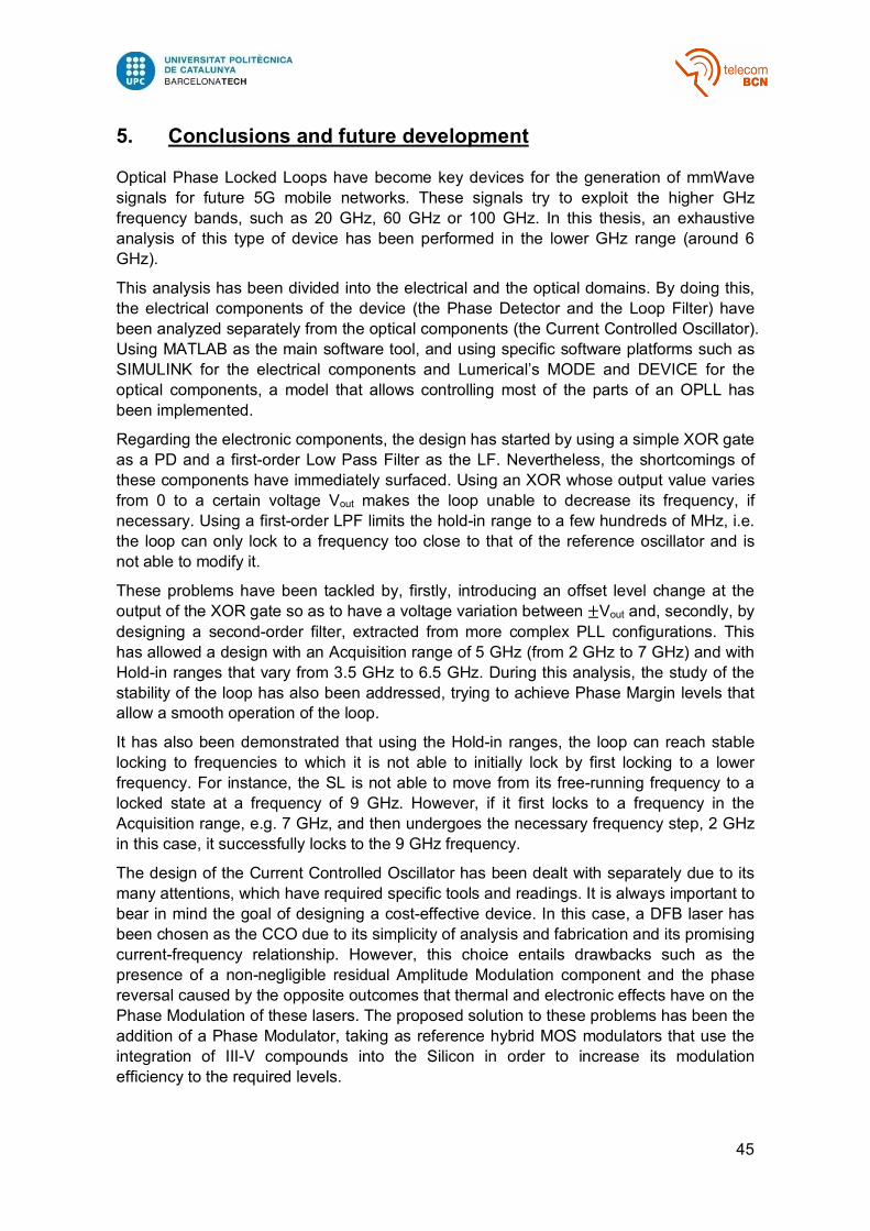
45
5. Conclusions and future development
Optical Phase Locked Loops have become key devices for the generation of mmWave signals for future 5G mobile networks. These signals try to exploit the higher GHz frequency bands, such as 20 GHz, 60 GHz or 100 GHz. In this thesis, an exhaustive analysis of this type of device has been performed in the lower GHz range (around 6 GHz).
This analysis has been divided into the electrical and the optical domains. By doing this, the electrical components of the device (the Phase Detector and the Loop Filter) have been analyzed separately from the optical components (the Current Controlled Oscillator). Using MATLAB as the main software tool, and using specific software platforms such as SIMULINK for the electrical components and Lumerical’s MODE and DEVICE for the optical components, a model that allows controlling most of the parts of an OPLL has been implemented.
Regarding the electronic components, the design has started by using a simple XOR gate as a PD and a first-order Low Pass Filter as the LF. Nevertheless, the shortcomings of these components have immediately surfaced. Using an XOR whose output value varies from 0 to a certain voltage Vout makes the loop unable to decrease its frequency, if necessary. Using a first-order LPF limits the hold-in range to a few hundreds of MHz, i.e. the loop can only lock to a frequency too close to that of the reference oscillator and is not able to modify it.
These problems have been tackled by, firstly, introducing an offset level change at the output of the XOR gate so as to have a voltage variation between ±Vout and, secondly, by designing a second-order filter, extracted from more complex PLL configurations. This has allowed a design with an Acquisition range of 5 GHz (from 2 GHz to 7 GHz) and with Hold-in ranges that vary from 3.5 GHz to 6.5 GHz. During this analysis, the study of the stability of the loop has also been addressed, trying to achieve Phase Margin levels that allow a smooth operation of the loop.
It has also been demonstrated that using the Hold-in ranges, the loop can reach stable locking to frequencies to which it is not able to initially lock by first locking to a lower frequency. For instance, the SL is not able to move from its free-running frequency to a locked state at a frequency of 9 GHz. However, if it first locks to a frequency in the Acquisition range, e.g. 7 GHz, and then undergoes the necessary frequency step, 2 GHz in this case, it successfully locks to the 9 GHz frequency.
The design of the Current Controlled Oscillator has been dealt with separately due to its many attentions, which have required specific tools and readings. It is always important to bear in mind the goal of designing a cost-effective device. In this case, a DFB laser has been chosen as the CCO due to its simplicity of analysis and fabrication and its promising current-frequency relationship. However, this choice entails drawbacks such as the presence of a non-negligible residual Amplitude Modulation component and the phase reversal caused by the opposite outcomes that thermal and electronic effects have on the Phase Modulation of these lasers. The proposed solution to these problems has been the addition of a Phase Modulator, taking as reference hybrid MOS modulators that use the integration of III-V compounds into the Silicon in order to increase its modulation efficiency to the required levels.
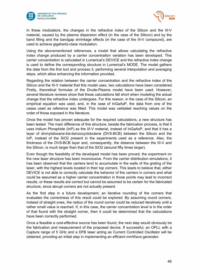
46
In these modulators, the changes in the refractive index of the Silicon and the III-V material, caused by the plasma dispersion effect (in the case of the Silicon) and by the band filling and the bandgap shrinkage effects (in the case of the III-V compound), are used to achieve gigahertz-class modulation.
Using the abovementioned references, a model that allows calculating the refractive index change produced by a carrier concentration variation has been developed. This carrier concentration is calculated in Lumerical’s DEVICE and the refractive index change is used to define the corresponding structure in Lumerical’s MODE. The model gathers the data from the first tool and process it, performing several interpolation and averaging steps, which allow enhancing the information provided.
Regarding the relation between the carrier concentration and the refractive index of the Silicon and the III-V material that this model uses, two calculations have been considered. Firstly, theoretical formulas of the Drude-Plasma model have been used. However, several literature reviews show that these calculations fall short when modeling the actual change that the refractive index undergoes. For this reason, in the case of the Silicon, an empirical equation was used, and, in the case of InGaAsP, the data from one of the cases used as reference was fitted. This model was validated reaching values on the order of those exposed in the literature.
Once the model has proven adequate for the required calculations, a new structure has been tested. The main difference of this structure, beside the fabrication process, is that it uses Indium Phosphide (InP) as the III-V material, instead of InGaAsP, and that it has a layer of divinylsiloxane-bis-benzocyclobutene (DVS-BCB) between the Silicon and the InP, instead of the SiO2 present in the experiments used as a reference. Also, the thickness of the DVS-BCB layer and, consequently, the distance between the III-V and the Silicon, is much larger than that of the SiO2 (around fifty times larger).
Even though the feasibility of the developed model has been proved, the experiment on the new laser structure has been inconclusive. From the carrier distribution simulations, it has been observed that the carriers tend to accumulate in the walls of the grating of the laser, with the highest levels located in their top corners. This leads to believe that, either DEVICE is not able to correctly calculate the behavior of the carriers in corners and what could be assumed as a higher carrier concentration in those points may lead to incorrect results, or these results are correct but cannot be assumed to be certain for the fabricated structure, since abrupt corners are not actually present.
As the first step in a future development, an iterative rounding of the corners that evaluates the correctness of this result could be explored. By assuming round corners, instead of straight ones, the radius of the round corner could be reduced iteratively until a rather small value is reached. If, in this case, the carrier concentration level is in the order of that found with the straight corner, then it could be determined that the calculations have been correctly performed.
Once a feasible a cost-effective source has been found, the next step would obviously be the fabrication and measurement of the proposed device. If successful, an OPLL with a Capture range of 5 GHz and a DFB laser acting as Current Controlled Oscillator will be obtained, providing an initial step in implementing an efficient mmWave generator.
47
Bibliography
[1]. G. Brown (2016). Exploring the Potential of mmWave for 5G Mobile Access [White paper]. [Online] Available: https://www.qualcomm.com/invention/5g/resources [Accessed: March 2018]
[2]. M. Mohamed, B. Hraimel, X. Zhang, M. N. Sakib, K. Wu, “Frequency Quadrupler for Millimeter-Wave Multiband OFDM Ultrawideband Wireless Signals and Distribution Over Fiber Systems”, IEEE/OSA Journal Optical Communication Networks, vol. 1, pp. 428-438, October 2009.
[3]. R. Sambaraju, J. Herrera, J. Marti, D. Zibar, A. Caballero, J. B. Jensen, T. Monroy, “Up to 40 Gb/s Wireless Signal Generation and Demodulation in 75-110 GHz Band using Photonic Techniques”, in IEEE Topical Meeting on Microwave Photonics (MWP), pp. 1-4, October 2010.
[4]. A. Hirata, H. Tkahasi, R. Yamaguchi, T. Kosugi, K. Murata, T. Nagatsuma, N. Kukutsu, Y. Kado, “Transmission Characteristics of 120-GHz-Band Wireless Link Using Radio-on-Fiber Technologies”, Journal Lightwave Technology, vol. 26, pp. 2338-2344, August 2008.
[5]. A. Hirata, T. Kosugi, H. Takahasi, J. Takeuchi, H. Togo, M. Yaita, N. Kukutsu, K. Aihara, K. Murata, Y. Sato, T. Nagatsuma, Y. Kado, “120-GHz-band wireless link technologies for outdoor 10-Gbit/s data transmission”. IEEE Transactions. Microwave Theory Techniques, vol. 60, no. 3, pp. 881-895, Mar. 2012.
[6]. H. J. Song, T. Nagatsuma, “Present and future of Terahertz communications”, IEEE Trans. Terahertz Sci. Technol., vol. 1, no. 1, pp. 256-263, Sep. 2011.
[7]. L. Ponnampalam, R. J. Steed, M. Fice, C. Renaud, D. C. Rogers, D. G. Moodie, G. D. Maxwell, I. F. Lealman, “A compact tunable coherent Terahertz source based on an hybrid integrated optical Phase-lock loop”, in Topical Meeting on Microwave Photonics (MWP), 2010, pp. 151-154.
[8]. L. Ponnampalam, M. Fice, F. Pozzi, C. Renaud, D. Rogers, I. F. Lealman, D. G. Moodie, P. J. Cannard, C. Lynch, L. Johnston, M. J. Robertson, R. Cornin, L. Pavlovic, L. Naglic, M. Vidmar, A. Seeds. “Monolithically integrated photonic heterodyne system”, Journal Lightwave Technology, vol. 29, no. 15, pp. 2229-2234, Aug. 2011.
[9]. U. Gliese, T. Nielsen, M. Bruun, E. L. Christensen, K. E. Stubkjzr, S. Lindgren, B. Broberg, “A wideband heterodyne optical phase-locked loop for generation of 3-18 GHz microwave carriers”, Photonics Technology Letters, vol. 14, no.8, pp.936-938, 1992.
[10]. P. T. Dat, A. Kanno, T. Umezawa, N. Yamamoto, T. Kawanishi. “Millimeter- and Terahertz-wave Radio-over-Fiber for 5G and Beyond”, Photonics Scoiety Summer Topical Meeting Series (SUM), 2017, pp. 165-166. DOI: 10.1109/PHOSST.2017.8012702
[11]. P. T. Dat, A. Kanno, T. Kawanishi. “Radio-on-radio-over-fiber: an efficient fronthauling for smart cells and moving cells”, IEEE Wireless Communications, vol. 22, Iss. 5, October 2016, pp. 67-74
48
[12]. M. J. Fice, A. Chiuchiarelli, E. Ciameramella, A. J. Seeds, “Homodyne coherent optical receiver using an optical injection Phase-lock loop”. Journal Lightwave Technology, vol. 29, no. 8, pp. 1152-1164, 2011.
[13]. Y. Shoji, M. J. Fice, Y. Takayama, A. J. Seeds, A. A. Leo, “A pilot-Carrier Coherent LEO-to-Ground Downlink System Using an Optical Injection Phase Lock”, Journal Lightwave Technology, vol. 30, no. 16, pp. 2696-2706, 2012.
[14]. G. J. Schneider, J. A. Murakowski, C. A. Schuetz, S. Shi, D. W. Prather, “Radiofrequency signal-generation system with over seven octaves of continuous tuning”, Nature Photonics, vol. 7, no. January, pp. 118-122, 2013
[15]. C. J. Buczek, R. J. Freiberg and E. Bonek, “Frequency synchronization and phase locking of CO2 lasers”, Applied Physics Letters, vol. 41, no. 7, p. 592, 1982
[16]. K. Balakier, M. J. Fice, F. van Dijk, G. Kervella, G. Carpintero, A. J. Seeds, C. C. Renaud, “Optical injection locking of monolithically integrated photonic source for generation of high purity signals above 100 GHz”, Optics Express, vol. 22, no. 24, p. 29404, 2014.
[17]. S. Fukushima, C. Silva, Y. Muramoto, A. J. Seeds, “Optoelectronic millimeter-wave synthesis using an optical frequency comb generator, optically injection locked laser, and a unitravelling-carrier photodiode”, Journal Lightwave Technology, vol. 21, no. 12, pp. 3043-3051, 2003.
[18]. K. Balakier, L. Ponnampalam, M. J. Fice, C. C. Renaud, A. J. Seeds, “Integrated Semiconductor Laser Optical Phase Lock Loops”, IEEE Journal of Selected Topics in Quantum Electronics, vol. 24, Iss. 1, Jan.-Feb. 2018.
[19]. K. Balakier, M. J. Fice, L. Ponnampalam, A. J. Seeds, C. C. Renaud, “Monolithically integrated optical phase lock loop for microwave photonics”, Journal Lightwave Technology, vol. 32, no. 20, pp. 3893-3900, Oct. 2014.
[20]. A. Rolland, G. Loas, L. Frein, M. Vallet, M. Brunel, M. Alaouini, “Optoelectronic phase-locked loop for millimeter-wave and Terahertz beat note stabilization”, Proceedings of SPIE, 2012, vol. 8496, p. 84960H-6.
[21]. A. J. Seeds, M. J. Fice, K. Balakier, M. Natrella, O. mitrofanov, M. Lamponi, M. Chtioui, F. van Dijk, M. Pepper, G. Aeppli, G. Davies, P. Dean, E. Linfield, C. C. Renaud, “Coherent terahertz photonics”, Optics Express, vol. 21, no.19, pp. 22988-23000, Sep. 2013.
[22]. H. R. Telle, D. Meschede, T. W. Hänsch, “Realization of a new concept for visible frequency division: phase locking of harmonic and sum frequencies”, Optical Letters, vol. 15, no. 10, pp. 532-534, 1990.
[23]. N. Satyan, “Optoelectronic Control of the Phase and Frequency of Semiconductor Lasers”, Ph. D. dissertation, California Institute of Technology, Pasadena, CA, USA, 2011
[24]. S. Tanaka, T. Akiyama, S. Sekiguchu, K. Morito, “Silicon photonics optical transmitter technology for Tb/s-class I/O co-packaged with CPU”, FUJITSU Scientific and Technical Journal, vol. 50, pp. 123-131, 2014.
[25]. T. Komljenovic, S. Srinivasan, E. Norberg, M. Davenport, G. Fish, J. Bowers. “Widely tunable narrow-linewidth monolithically integrated external-cavity
49
semiconductor lasers”, IEEE Journal of Selected Topics in Quantum Electronics, vol. 21, pp. 1-9, 2015.
[26]. Z. Wang, B. Tian, M. Paladugu, M. Pantouvaki, N. Le Thomas, C. Guo, J. Dekoster, J. van Campenhout, P. Absil, “Polytypic InP nano-laser monolithically integrated on (001) silicon” Nano Letters, vol. 13, pp. 5063-5069, 2013.
[27]. G. Roelkens, A. Abassi, P. Cardille, U. Dave, A. de Groote, Y. de Koninck, S. Dhoore, X. Fu, A. Gasseng, N. Hattasan, Q. Huang, S. Kumari, S. Keyvaninia, B. Kuyken, L. Li, M. Tassaert, K. van Gasse, J. Verbist, R. Wang, Z. Wang, J. Zhang, J. van Campenhout, X. Yin, J. Bauwelinck, G. Morthier, R. Baets, D. van Thourhout, “III-V-on-Silicon Photonic Devices for Optical Communications and Sensing”, Photonics, vol. 2, pp. 969-1004, 2015.
[28]. J. H. Han, F. Boeuf, J. Fujikata, S. Takahashi, S. Takagi, M. Takenaka, “Efficient low-loss InGaAsP/Si hybrid MOS optical modulator”, Nature Photonics, vol. 11, pp. 486-490 August 2017. DOI: 10.1038/NPHOTON.2017.122
[29]. T. Hiraki, T. Aihara, K. Hasebe, K. Takeda, T. Fujii, T. Kakitsuka, T. Tsuchizawa, H. Fukuda, S. Matsuo, “Heterogeneously integrated III-V/Si MOS capacitor Mach-Zehnder modulator”, Nature Photonics, vol. 11, pp. 482-485, August 2017. DOI: 10.1038/NPHOTON.2017.120
[30]. T. L. Koch and J. E. Bowers, “Nature of wavelength chirping in directly modulated semiconductor lasers”, Electronic Letters, vol. 20, Iss. 25, pp. 1038-1040, December 1984, DOI: 10.1049/el:19840709
[31]. P. Correc, O. Girard, I. F. de Faria Jr., “On the thermal contribution to the FM response of DFB lasers: Theory and experiment”, IEEE Journal of Quantum Electronics, vol. 30, no. 11, November 1990.
[32]. Agilent Technologies (2003). “Understanding Jitter and Wander Measurements and Standards”. [Brochure]
[33]. A. Lerín, G. Y. Chu, V. Polo, I. Cano and J. Prat, “Chip integrated DFB-EAM for directly phase modulation performance improvement in UDWDM-PON”, presented at the Optical Fiber Communications Conference, Valencia, Spain, 2015, Paper P.7.10.
[34]. G. T. Reed, D. J. Thomson, F. Y. Gardes, Y. Hu, J. M. Fedeli and G. Z. Mashanovic “High-speed carrier-depletion silicon Mach-Zehnder optical modulators with lateral PN junctions”, Frontiers in Physics, 2:77, DOI: 10.3389/fphy.2914.00077
[35]. S. Akiyama and T. Usuki, “High-speed and efficient silicon modulator based on forward-biased pin diodes” Frontiers in Physics, 2:65, DOI: 10.3389/fphy.2014.00065
[36]. M. Webster, P. Gothoskar, V. Patel, D. Piede, S. Anderson, R. Tummidi, D. Adams, C. Appel, P. Metz, S. Sunder, B. Dama and K. Shastri, “An efficient MOS-capacitor based silicon modulator and CMOS drivers for optical transmitters”, in International Conference Group IV Photonics WB1, (IEEE, 2014).
[37]. M. Webster, C. Appel, P. Gothoskar, S. Sunder, B. Dama, K. Shastri, “Silicon Photonics Modulator based on a MOS-Capacitor and a CMOS driver”, in Compound Semiconductor Integrated Circuit Symposium, E. 3 (IEEE, 2014).
50
[38]. C. H. Henry, R. A. Logan and K. A. Bertness, “Spectral dependence of the change in refractive index due to carrier injection in GaAs lasers”, Journal of Applied Physics, vol. 52, pp. 4457-4461, 1981.
[39]. Q. Lin, O. J. Painter and G. P. Agrawal, “Nonlinear optical phenomena in silicon waveguides: Modeling and applications”, Optics Express, vol. 15, no. 25, pp. 16604-16644, December 2007.
[40]. B. R. Bennet, R. A. Soref and J. A. Del Álamo, “Carrier-Induced Change in Refractive Index of InP, GaAs, and InGaAsP”, IEEE Journal of Quantum Electronics, vol. 26, no. 1, pp. 113-122, January 1999.
[41]. C. Van Praet, “Energieverlagende Techniken in Toegangsnetwrken van de volgende generatie”, Ph. D dissertation, Ghent Universiteit, Department of Information Technology, Ghent, Belgium, 2014
[42]. Lumerical Knowledge Base, “Import object – Spatial (n, k) data”, [Accessed January 2018] https://kb.lumerical.com/en/index.html?ref_sim_obj_importing_spatial _nk.html
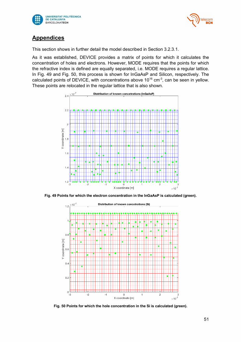
51
Appendices
This section shows in further detail the model described in Section 3.2.3.1.
As it was established, DEVICE provides a matrix of points for which it calculates the concentration of holes and electrons. However, MODE requires that the points for which the refractive index is defined are equally separated, i.e. MODE requires a regular lattice. In Fig. 49 and Fig. 50, this process is shown for InGaAsP and Silicon, respectively. The calculated points of DEVICE, with concentrations above 1016 cm-3, can be seen in yellow. These points are relocated in the regular lattice that is also shown.
Fig. 49 Points for which the electron concentration in the InGaAsP is calculated (green).
Fig. 50 Points for which the hole concentration in the Si is calculated (green).
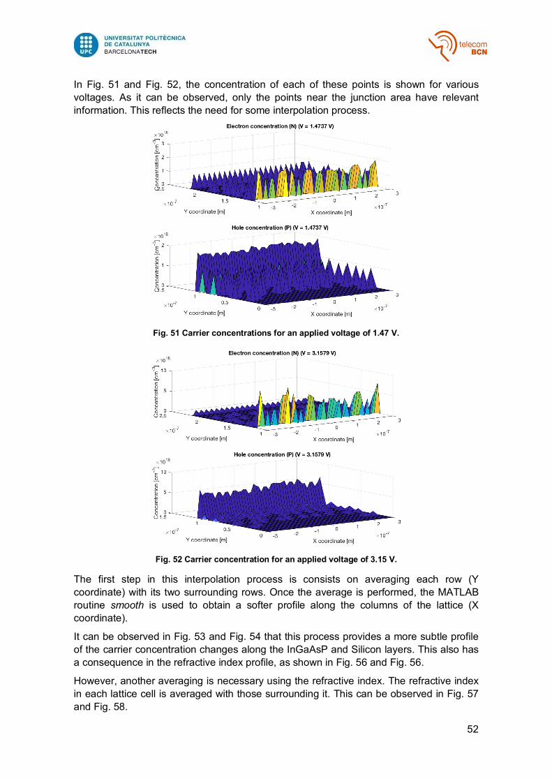
52
In Fig. 51 and Fig. 52, the concentration of each of these points is shown for various voltages. As it can be observed, only the points near the junction area have relevant information. This reflects the need for some interpolation process.
Fig. 51 Carrier concentrations for an applied voltage of 1.47 V.
Fig. 52 Carrier concentration for an applied voltage of 3.15 V.
The first step in this interpolation process is consists on averaging each row (Y coordinate) with its two surrounding rows. Once the average is performed, the MATLAB routine smooth is used to obtain a softer profile along the columns of the lattice (X coordinate).
It can be observed in Fig. 53 and Fig. 54 that this process provides a more subtle profile of the carrier concentration changes along the InGaAsP and Silicon layers. This also has a consequence in the refractive index profile, as shown in Fig. 56 and Fig. 56.
However, another averaging is necessary using the refractive index. The refractive index in each lattice cell is averaged with those surrounding it. This can be observed in Fig. 57 and Fig. 58.
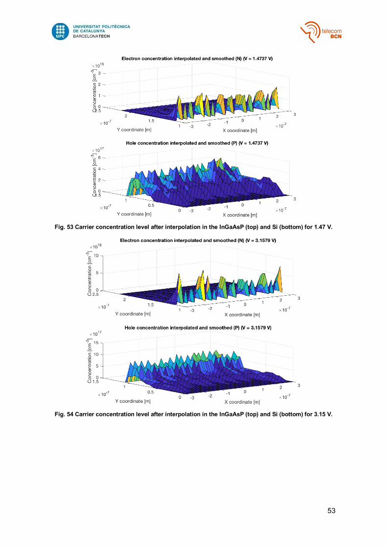
53
Fig. 53 Carrier concentration level after interpolation in the InGaAsP (top) and Si (bottom) for 1.47 V.
Fig. 54 Carrier concentration level after interpolation in the InGaAsP (top) and Si (bottom) for 3.15 V.
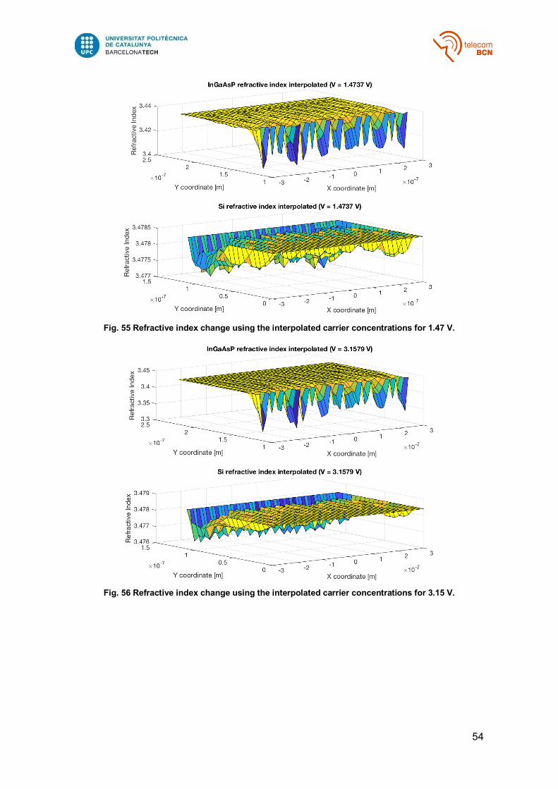
54
Fig. 55 Refractive index change using the interpolated carrier concentrations for 1.47 V.
Fig. 56 Refractive index change using the interpolated carrier concentrations for 3.15 V.
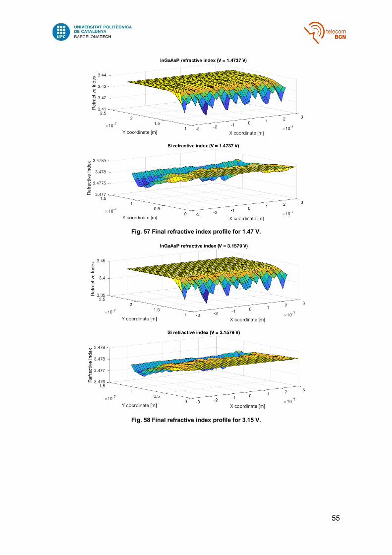
55
Fig. 57 Final refractive index profile for 1.47 V.
Fig. 58 Final refractive index profile for 3.15 V.
56
Glossary
CCO Current Controlled Oscillator
RoF Radio over Fiber
SCL Semiconductor Laser
OPLL Optical Phase Locked Loop
OIL Optical Injection Locking
OIPLL Optical Injection Phase Locked Loop
SL Slave Laser
ML Master Laser
PLL Phase Locked Loop
DFB Distributed Feedback
DBR Distributed Bragg Refractor
AM Amplitude Modulation
FM Frequency Modulation
PM Phase Modulation
MOS Metal Oxide Semiconductor
BBU Baseband Unit
BS Base Station
CS Central Station
RAT Random Access Technology
ODN Optical Distribution Network
PIC Photonic Integrated Circuit
BOX Buried Oxide
TE Transversal Electric
PD Phase Detector
VCO Voltage Controlled Oscillator
LF Loop Filter
LPF Low Pass Filter
GCP Gain Crossover Point
PCP Phase Crossover Point
EAM Electro-Absorption Modulator
FDE Finite Difference Eigensolver
SOI Silicon on Insulator


![DESIGN AND ANALYSIS OF EFFICIENT PHASE LOCKED LOOP … · Phase Locked Loop (PLL) mainly for synchronization, clock synthesis, skew and jitter reduction [5]. Phase locked loops find](https://img.pdfslide.net/doc/110x75/5e9d540ca2a49a4e746bfacd/design-and-analysis-of-efficient-phase-locked-loop-phase-locked-loop-pll-mainly.jpg)