Embed Size (px)
Citation preview

Department of Electrical and Computer Engineering
July, 2018
Design Rules for PCB Layout Using Altium Designer 1.0 Introduction The Department currently has an in-house facility for making PCBs which permits boards to be made relatively quickly at low cost. This facility does have some limitations, though, which in turn places some constraints upon PCB layout. This document outlines these constraints and how to implement them. It also discusses how to check your work, how to save it, as well as what you need to do in order to have your PCB design made. Depending on who will manufacture your PCB there will be certain manufacturing limitations, which in turn will place constraints on your PCB layout. These constraints can be easily satisfied by altering some of the default design rules in Altium. This document outlines some of the most important constraints and how to implement them. It also discussed how to check your work, how to save it, as well as what you need to do in order to have your PCB design made. Subsequent sections of this document discuss the following aspects:
• Minimum clearance between all tracks, pads and components.
• Interactive routing track width & via sizes
• Track widths for different nets (supply nets, signal nets etc)
• Routing via style
• Polygon properties if using a polygon plane
• Silk to solder mask & silk to silk clearance
• Component pad sizes
• PCB outline, mounting requirements and identification
• Design rule checking
• Saving your work
• Submitting your design 2.0 Additional Things to note if PCB is Made In-House If you wish to use ECE department’s an in-house PCB facility, a few aspects need to be clarified. It does have a simple setup however there are some additional limitations imposed on your PCB layout. Firstly, the department’s in-house facility can only make single-sided PCBs or double-sided (using both top layer & bottom layers) PCBs. However, we currently does not have the capability to do plated through holes (PTH). For double-sided boards this means that any required connection between a bottom-layer track and a top-layer track happens by means of either a wire or a component lead soldered on both the top & bottom layers. In the latter case, one needs
Department of Electrical and Computer Engineering
July, 2018
to ensure that soldering on the top layer is actually possible. This is not the case for many components, including connectors & electrolytic capacitors. So it is important to ensure that any component that cannot be soldered on the top layer does not have a top layer track connected to it. Secondly, the Department does not have the facility to automatically drill your board once it has been made. You will need to do this yourself using drilling facilities available in the Department. 3.0 Minimum Clearance between all tracks, PADs and
components.
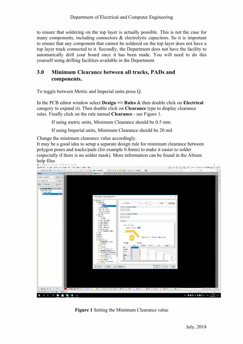
To toggle between Metric and Imperial units press Q. In the PCB editor window select Design >> Rules & then double click on Electrical category to expand it). Then double click on Clearance type to display clearance rules. Finally click on the rule named Clearance - see Figure 1.
If using metric units, Minimum Clearance should be 0.5 mm.
If using Imperial units, Minimum Clearance should be 20 mil. Change the minimum clearance value accordingly. It may be a good idea to setup a separate design rule for minimum clearance between polygon pours and tracks/pads (for example 0.8mm) to make it easier to solder (especially if there is no solder mask). More information can be found in the Altium help files
Figure 1 Setting the Minimum Clearance value
Department of Electrical and Computer Engineering
July, 2018
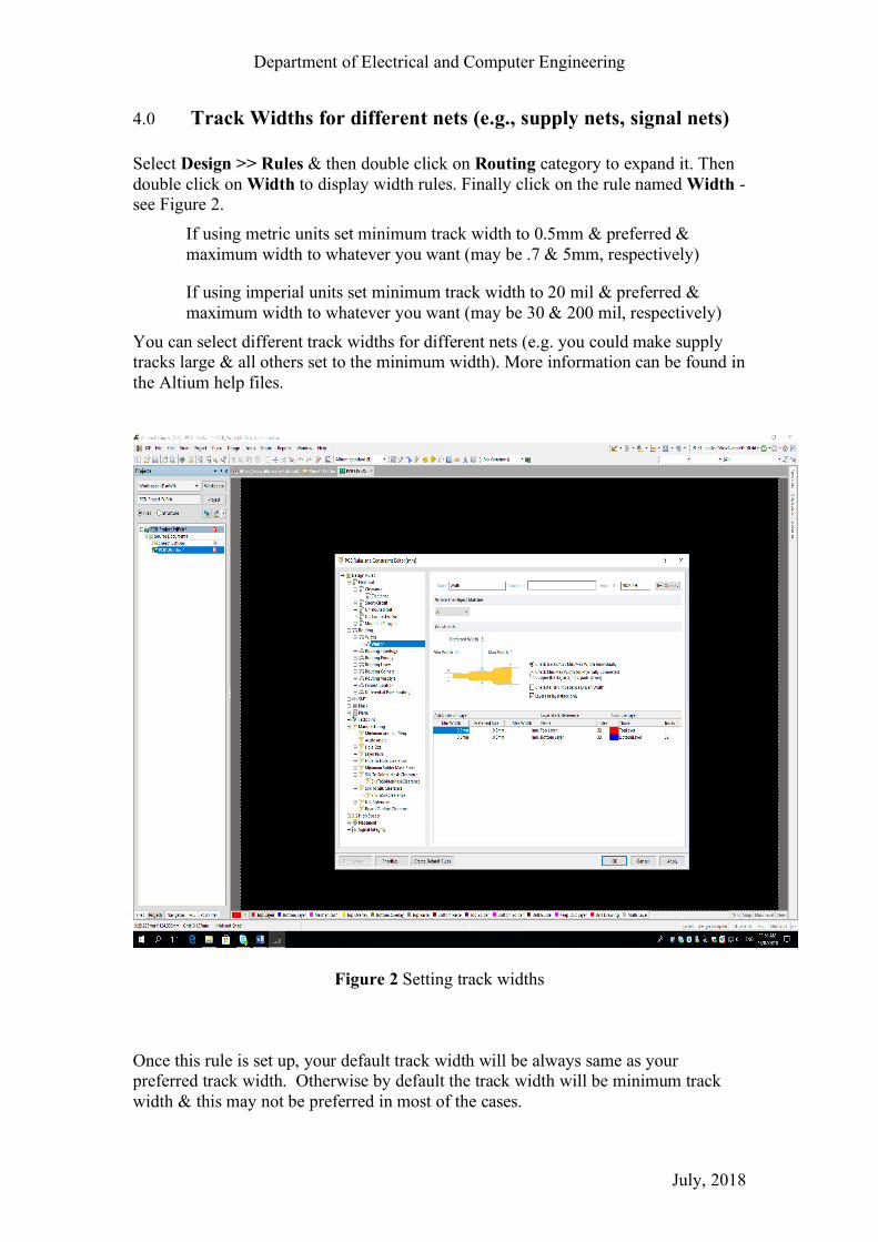
4.0 Track Widths for different nets (e.g., supply nets, signal nets) Select Design >> Rules & then double click on Routing category to expand it. Then double click on Width to display width rules. Finally click on the rule named Width - see Figure 2.
If using metric units set minimum track width to 0.5mm & preferred & maximum width to whatever you want (may be .7 & 5mm, respectively)
If using imperial units set minimum track width to 20 mil & preferred & maximum width to whatever you want (may be 30 & 200 mil, respectively)
You can select different track widths for different nets (e.g. you could make supply tracks large & all others set to the minimum width). More information can be found in the Altium help files.
Figure 2 Setting track widths
Once this rule is set up, your default track width will be always same as your preferred track width. Otherwise by default the track width will be minimum track width & this may not be preferred in most of the cases.

Department of Electrical and Computer Engineering
July, 2018
5.0 Routing Via Style Select Design >> Rules & then double click on Routing category to expand it. Then double click on routing via style to display width rules. Finally click on the rule named Routing Via, see Figure 3.
Set the minimum via diameter to 1.2mm, preferred via diameter to 1.7mm & maximum via diameter to 2.2mm Set the minimum via hole size to 0.6mm, preferred via hole size to 0.7mm & maximum via hole size to 1mm
Figure 3 Setting via size
Department of Electrical and Computer Engineering
July, 2018
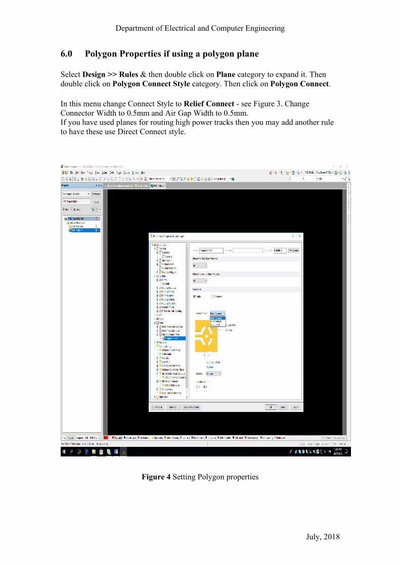
6.0 Polygon Properties if using a polygon plane Select Design >> Rules & then double click on Plane category to expand it. Then double click on Polygon Connect Style category. Then click on Polygon Connect. In this menu change Connect Style to Relief Connect - see Figure 3. Change Connector Width to 0.5mm and Air Gap Width to 0.5mm. If you have used planes for routing high power tracks then you may add another rule to have these use Direct Connect style.
Figure 4 Setting Polygon properties

Department of Electrical and Computer Engineering
July, 2018
7.0 Silk Clearances Select Design >> Rules & then double click on Manufacturing category to expand it. Then double click on Silk To Solder Mask Clearance and then click SilkToSolderMaskClearance In this menu change the clearance value to 0.1mm Then Double click on Silk To Silk Clearance and then click SilkToSilkClearance In this menu also change the clearance value to 0.1mm Note that you can make both of these values to 0mm if you want to ignore all the silk errors in your design.
Figure 5 Setting Silk Clearance 8.0 Hole size Be default the hole size (diameter) is 2.54mm which is not enough for mounting holes. This setting needs to be changed in design rules.
Department of Electrical and Computer Engineering
July, 2018
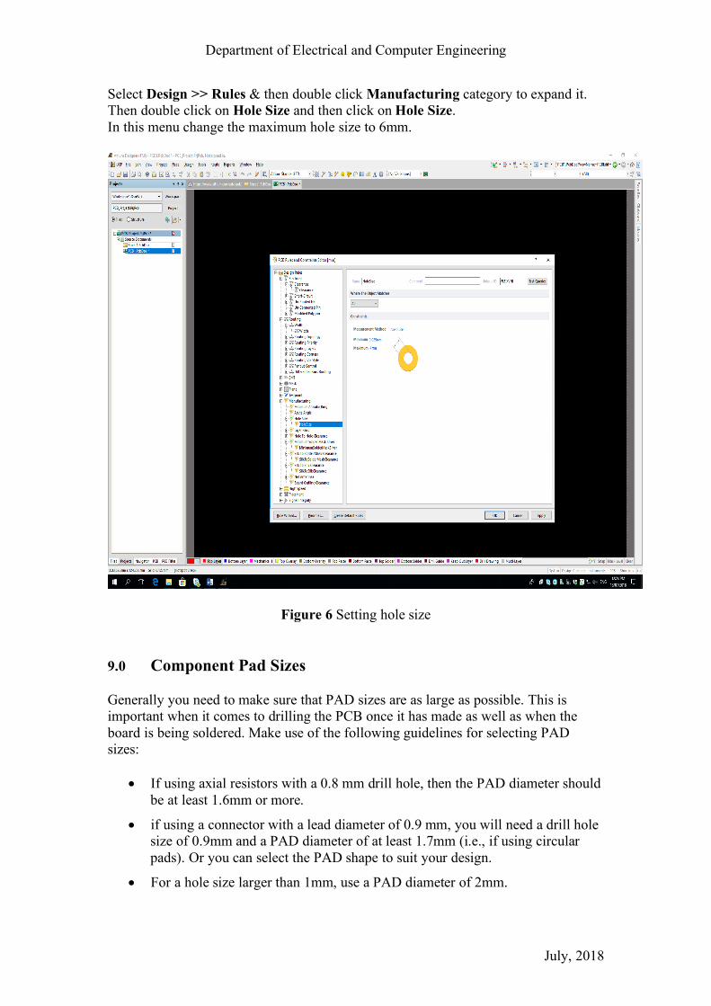
Select Design >> Rules & then double click Manufacturing category to expand it. Then double click on Hole Size and then click on Hole Size. In this menu change the maximum hole size to 6mm.
Figure 6 Setting hole size 9.0 Component Pad Sizes Generally you need to make sure that PAD sizes are as large as possible. This is important when it comes to drilling the PCB once it has made as well as when the board is being soldered. Make use of the following guidelines for selecting PAD sizes:
• If using axial resistors with a 0.8 mm drill hole, then the PAD diameter should be at least 1.6mm or more.
• if using a connector with a lead diameter of 0.9 mm, you will need a drill hole size of 0.9mm and a PAD diameter of at least 1.7mm (i.e., if using circular pads). Or you can select the PAD shape to suit your design.
• For a hole size larger than 1mm, use a PAD diameter of 2mm.
Department of Electrical and Computer Engineering
July, 2018
• For ICs, the hole size is normally 0.8 mm, but because the pins of an IC are adjacent to each other, in order to get maximum clearance between PADs, use oval shaped PADs rather than round. This can be achieved by setting the X size dimension of a PAD to be larger than the Y size. For example, for a 14 pin DIP package, use PAD X size = 2mm and PAD Y seize = 1.5mm, with a hole dimension = 0.8mm.
• For other components which are placed very close to each other, you should also select oval PADs in order to ensure maximum clearance between pads
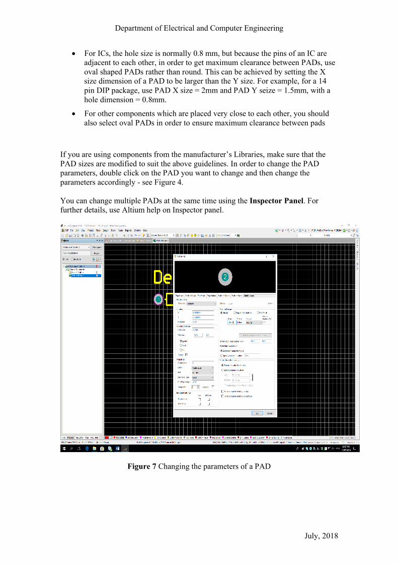
If you are using components from the manufacturer’s Libraries, make sure that the PAD sizes are modified to suit the above guidelines. In order to change the PAD parameters, double click on the PAD you want to change and then change the parameters accordingly - see Figure 4. You can change multiple PADs at the same time using the Inspector Panel. For further details, use Altium help on Inspector panel.
Figure 7 Changing the parameters of a PAD
Department of Electrical and Computer Engineering
July, 2018
10.0 PCB Outline, Mounting Requirements and Identification The following precautions should be taken when designing a PCB. PCB Outline Make sure that this is well defined and drawn in the Keep Out layer PCB Mounting Requirements You need to give careful thought as to how your PCB will be mounted and factor this into your design. This may be by way of mounting holes (use sizes of 3mm or 4mm typically). But other methods of PCB mounting are also acceptable.
PCB Identification To facilitate in identifying & distributing PCBs once they are made, make sure that your PCB is identified in the following manner:
• Part IV project students: Course Number / Project No. o examples: EE 401 / Prj 95, CS 401 / Prj 83, SE 401 / Prj 16
• Part III design students: Course No. / Group No. o examples: EE 310 / Grp 12, CS 301 / Grp 5
• All others: write their UPI or PCB title (whichever is convenient) The text used for identification can be placed either on the top or bottom layers. If placed on the Bottom layer, it should be mirrored, but if on the Top layer, it should not. 11.0 Design Rule Checking Once you have completed your PCB design, you need to verify that it complies with the design rules. Do this as follows: Choose Tools >> Design Rule Check & then click on Run Design Rule Check Design Rule check highlights any design violations in your design. If you have complied with all the design rules, there should be no rule violations. However, if in your design you have rule violations make sure to fixe these issues before submitting your PCB. 12.0 Submitting Your Design for Manufacture Before submitting your design for manufacture, you should complete the check list contained in Appendix A. Once you have completed your PCB design, you need to send the PCB file (.pcbdoc) to the project technician/submit via drop-box setup for the course so that your PCB can be made.
Department of Electrical and Computer Engineering
July, 2018
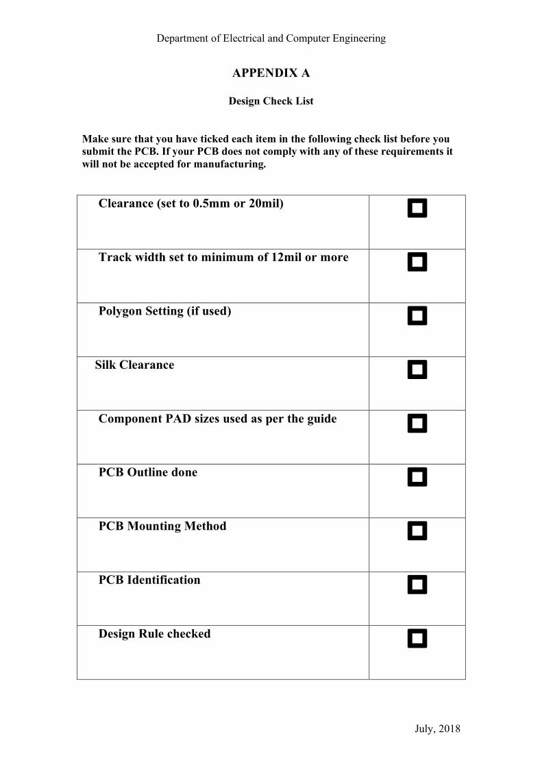
APPENDIX A
Design Check List Make sure that you have ticked each item in the following check list before you submit the PCB. If your PCB does not comply with any of these requirements it will not be accepted for manufacturing.
Clearance (set to 0.5mm or 20mil) o
Track width set to minimum of 12mil or more o
Polygon Setting (if used) o
Silk Clearance o
Component PAD sizes used as per the guide o
PCB Outline done o
PCB Mounting Method o
PCB Identification o
Design Rule checked o