Embed Size (px)
Citation preview

www.fairchildsemi.com
Designing the Power Train of a200W Power Supply with PFC
Michael WeirichGlobal Power Resource Center, Europe
2
Design issues for 200W PSU
System Specification• AC Input Voltage:
85 – 265 Vrms• Power-Factor: > 0.95• Total Output Power: 200W• Three DC Outputs:
• 5V/0.3A (standby)• 12V/6A,• 24V/5A
• Height limit: 25mm
Target application: LCD TV
Design Issues• System partitioning• Low profile boost inductor• PFC MOSFET dissipation• Using single switch forward
tools to design two-switch forward converters
• Two-switch forward drive• Second post-regulated output
for a forward converter• Auxiliary power supply• Layout
3
Control Component Overview
• PFC/two switch forward circuit• FAN4800 combined CCM PFC and current mode controller• FAN7382 dual high and low side driver
• Post regulation circuit• Low cost MC34063A controller with external MOSFET
• Auxiliary power supply• FSD210 Fairchild Power Switch
4
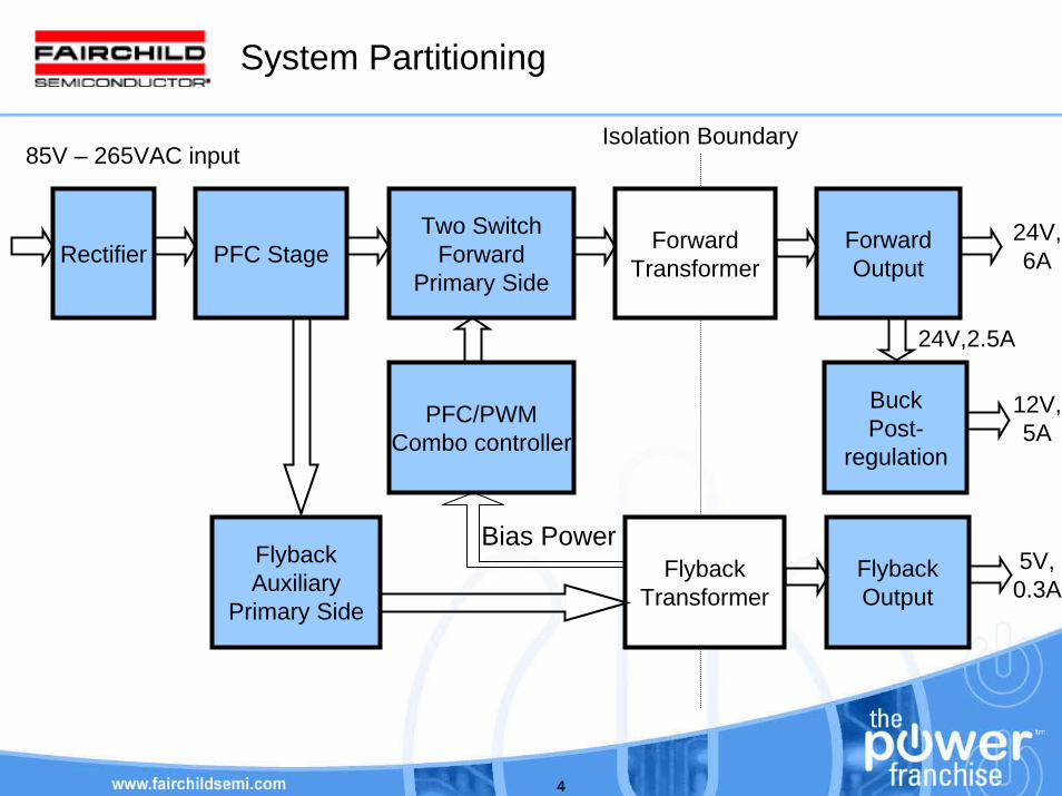
PFC StageTwo Switch
ForwardPrimary Side
Rectifier ForwardTransformer
ForwardOutput
85V – 265VAC input
24V,6A
BuckPost-
regulation
FlybackAuxiliary
Primary Side
FlybackTransformer
FlybackOutput
12V,5A
5V,0.3A
System Partitioning
Bias Power
PFC/PWMCombo controller
24V,2.5A
Isolation Boundary
5
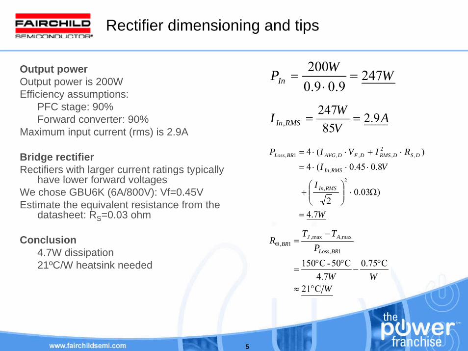
Rectifier dimensioning and tips
Output powerOutput power is 200WEfficiency assumptions:
PFC stage: 90%Forward converter: 90%
Maximum input current (rms) is 2.9A
Bridge rectifierRectifiers with larger current ratings typically
have lower forward voltagesWe chose GBU6K (6A/800V): Vf=0.45VEstimate the equivalent resistance from the
datasheet: RS=0.03 ohm
Conclusion4.7W dissipation21ºC/W heatsink needed
WWPIn 2479.09.0
200=
⋅=
AVWI RMSIn 9.2
85247
, ==
W
I
VIRIVIP
RMSIn
RMSIn
DSDRMSDFDAVGBRLoss
7.4
)03.02
8.045.0(4)(4
2,
,
,2
,,,1,
=
Ω⋅⎟⎟⎠
⎞⎜⎜⎝
⎛+
⋅⋅⋅=
⋅+⋅⋅=
WWW
PTT
RBRLoss
AJBR
C12
C0.757.4
C50-C1501,
max,max,1,
°≈
°−
°°=
−=Θ
6
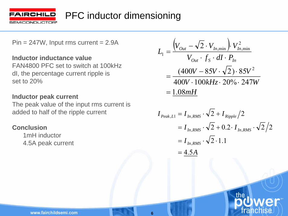
PFC inductor dimensioning
Pin = 247W, Input rms current = 2.9A
Inductor inductance valueFAN4800 PFC set to switch at 100kHz dI, the percentage current ripple isset to 20%
Inductor peak currentThe peak value of the input rms current isadded to half of the ripple current
Conclusion 1mH inductor4.5A peak current
( )
mHWkHzV
VVV
PdIfVVVV
LInSOut
InInOut
08.1247%20100400
85)285400(
2
2
2min,min,
1
=⋅⋅⋅⋅⋅−
=
⋅⋅⋅⋅⋅−
=
AI
II
III
RMSIn
RMSInRMSIn
RippleRMSInLPeak
5.41.12
222.02
22
,
,,
,1,
=
⋅⋅=
⋅⋅+⋅=
+⋅=
7
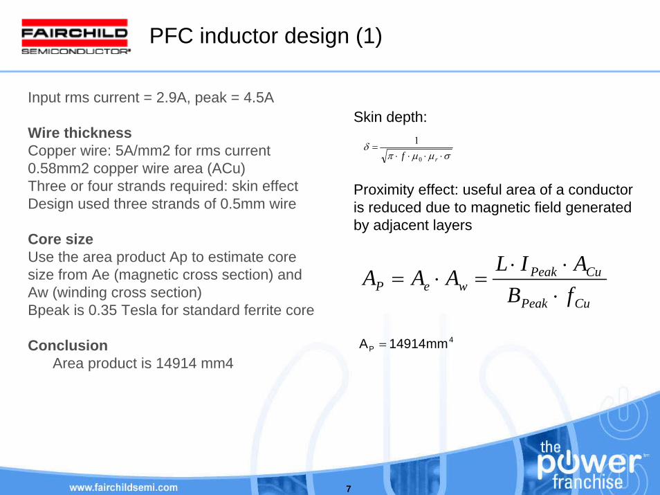
PFC inductor design (1)
Input rms current = 2.9A, peak = 4.5A
Wire thicknessCopper wire: 5A/mm2 for rms current0.58mm2 copper wire area (ACu)Three or four strands required: skin effectDesign used three strands of 0.5mm wire
Core sizeUse the area product Ap to estimate coresize from Ae (magnetic cross section) andAw (winding cross section)Bpeak is 0.35 Tesla for standard ferrite core
Conclusion Area product is 14914 mm4
σμμπδ
⋅⋅⋅⋅=
rf 0
1
4P mm14914A =
Skin depth:
Proximity effect: useful area of a conductor is reduced due to magnetic field generated by adjacent layers
CuPeak
CuPeakweP fB
AILAAA⋅⋅⋅
=⋅=
8
PFC inductor design (2)
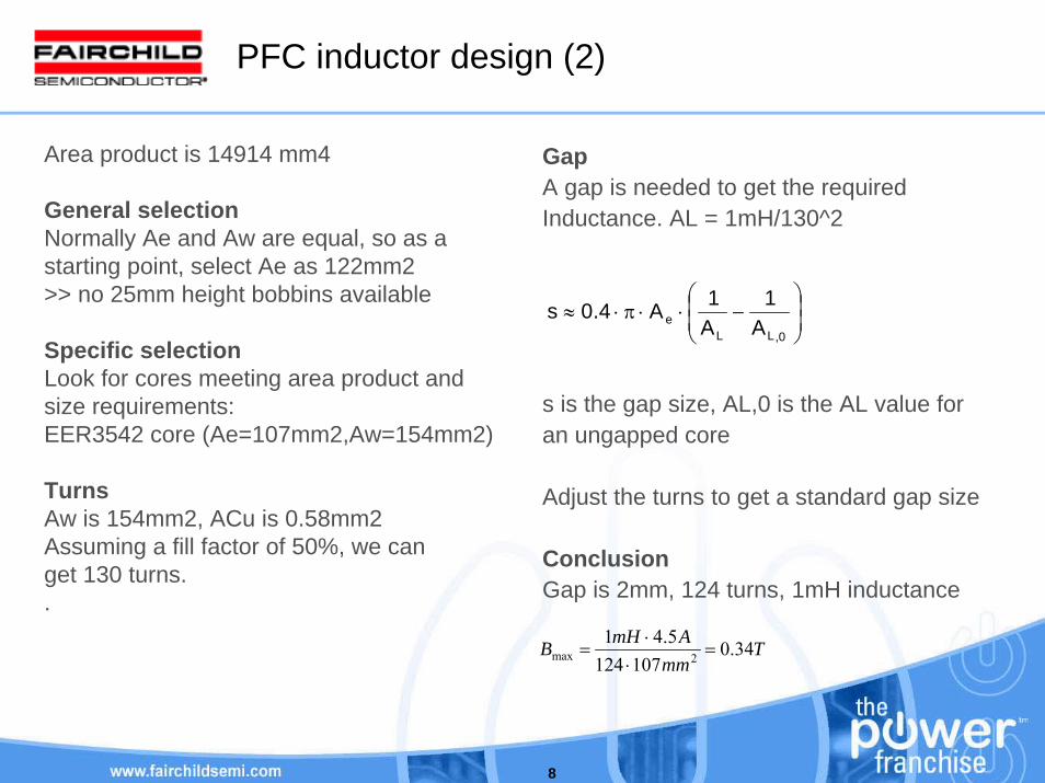
Area product is 14914 mm4
General selectionNormally Ae and Aw are equal, so as astarting point, select Ae as 122mm2>> no 25mm height bobbins available
Specific selectionLook for cores meeting area product andsize requirements:EER3542 core (Ae=107mm2,Aw=154mm2)
TurnsAw is 154mm2, ACu is 0.58mm2Assuming a fill factor of 50%, we canget 130 turns..
GapA gap is needed to get the requiredInductance. AL = 1mH/130^2
s is the gap size, AL,0 is the AL value foran ungapped core
Adjust the turns to get a standard gap size
ConclusionGap is 2mm, 124 turns, 1mH inductance
⎟⎟⎠
⎞⎜⎜⎝
⎛−⋅⋅π⋅≈
0,LLe A
1A1A4.0s
TAmHB 34.05.41=
⋅=
mm107124 2max ⋅
9
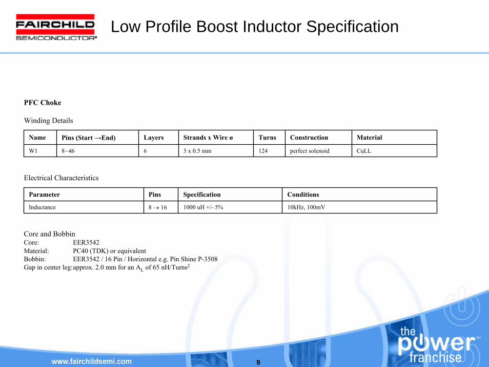
Low Profile Boost Inductor Specification
PFC Choke
Winding Details
Name Pins (Start →End) Layers Strands x Wire ø Turns Construction Material
W1 8 →16 6 3 x 0.5 mm 124 perfect solenoid CuLL
Electrical Characteristics
Parameter Pins Specification Conditions
Inductance 8 → 16 1000 uH +/- 5% 10kHz, 100mV
Core and BobbinCore: EER3542 Material: PC40 (TDK) or equivalentBobbin: EER3542 / 16 Pin / Horizontal e.g. Pin Shine P-3508Gap in center leg:approx. 2.0 mm for an AL of 65 nH/Turns2
10
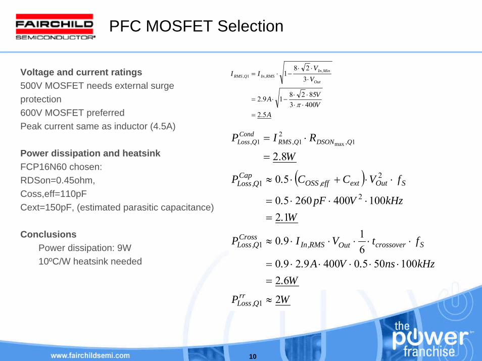
PFC MOSFET Selection
Voltage and current ratings500V MOSFET needs external surge protection600V MOSFET preferredPeak current same as inductor (4.5A)
Power dissipation and heatsinkFCP16N60 chosen:RDSon=0.45ohm, Coss,eff=110pFCext=150pF, (estimated parasitic capacitance)
ConclusionsPower dissipation: 9W10ºC/W heatsink needed
AVVA
VV
IIOut
MinInRMSInQRMS
5.24003
852819.2
328
1 ,,1,
=⋅⋅⋅⋅
−⋅=
⋅
⋅⋅−⋅=
π
W
RIP QDSONQRMSCond
QLoss
8.21,
21,1, max
=
⋅=
( )
W.kHzns.VA..
ftVI.P
W.kHzVpF.
fVCC.P
ScrossoverOutRMS,InCross
Q,Loss
SOutexteff,OSSCap
Q,Loss
6210050504009290
6190
1210040026050
50
1
2
21
=⋅⋅⋅⋅⋅=
⋅⋅⋅⋅⋅≈
=⋅⋅⋅=
⋅⋅+⋅≈
WPrrQ,Loss 21 ≈
11
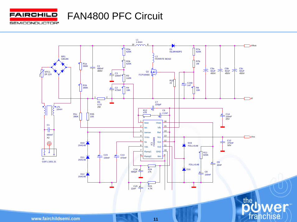
FAN4800 PFC Circuit
-+
~ ~
BR1GBU6K
D15FDLL4148
D1ISL9R460P2
R810K
D101N4148
D111N4148
C2470nF
D121N4148
Ieao1
Iac2
Isense3
Vrms4
Ss5
Vdc6
Ramp17
Ramp28 Ilim 9GND 10
Vo211
Vo1 12Vcc 13Ref 14Vfb 15
Veao16
IC1
FAN
4800
C62.2nFR1c
390K
R2427k
C16680pF
R3110K
R7b1MR1a
390K
D16
FDLL4148
C23100nF
R2a620K
R2b620K
+ C5c82uF450V
C12470nF50V
C14100nF25V
R1247K
C2680nF400V
C13470nF
NTC12R 12A
C2481nF
R7a620K
+ C5b82uF450V
R1b390K R4
18K
R11820K
C1
680nFX2
C7220pF
R234.7K
LF110mH
C1522nF
1 2
R50.152W
C8100nF
+ C5a82uF450V
R35100
816
L11.0mH
L3FERRITE BEAD
J1GSF1.1001.31
C3100nF
C910nF
R1522
Q1FCP16N60
Vcc
Vbus
0
12
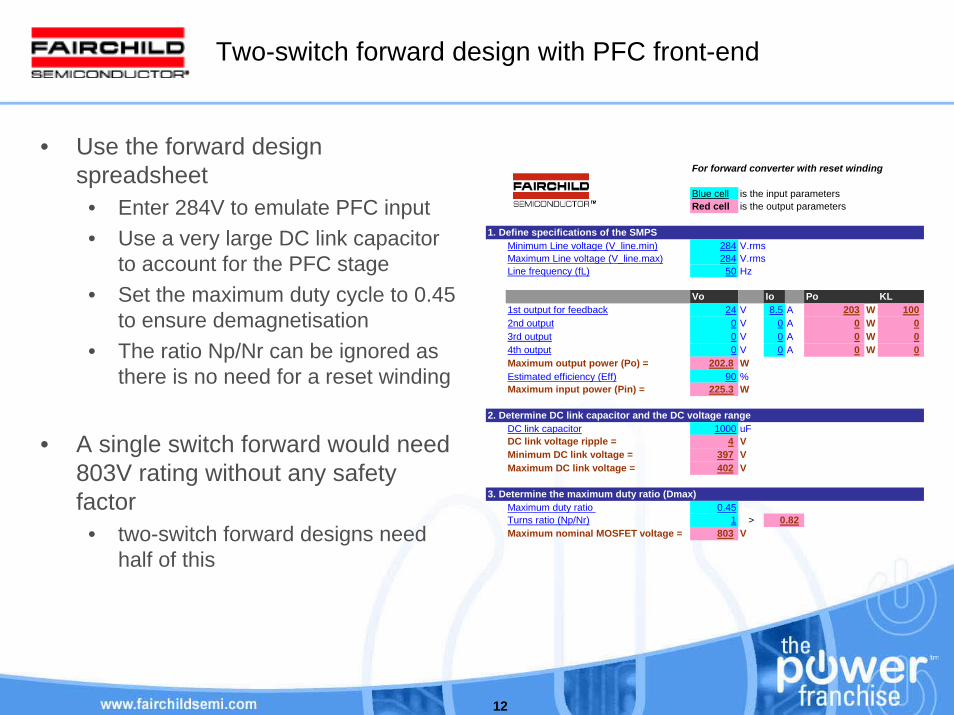
Two-switch forward design with PFC front-end
• Use the forward design spreadsheet
• Enter 284V to emulate PFC input• Use a very large DC link capacitor
to account for the PFC stage• Set the maximum duty cycle to 0.45
to ensure demagnetisation• The ratio Np/Nr can be ignored as
there is no need for a reset winding
• A single switch forward would need 803V rating without any safety factor
• two-switch forward designs need half of this
For forward converter with reset winding
Blue cell is the input parametersRed cell is the output parameters
1. Define specifications of the SMPSMinimum Line voltage (V_line.min) 284 V.rmsMaximum Line voltage (V_line.max) 284 V.rmsLine frequency (fL) 50 Hz
Vo Io Po KL1st output for feedback 24 V 8.5 A 203 W 1002nd output 0 V 0 A 0 W 03rd output 0 V 0 A 0 W 04th output 0 V 0 A 0 W 0Maximum output power (Po) = 202.8 WEstimated efficiency (Eff) 90 %Maximum input power (Pin) = 225.3 W
2. Determine DC link capacitor and the DC voltage rangeDC link capacitor 1000 uFDC link voltage ripple = 4 VMinimum DC link voltage = 397 VMaximum DC link voltage = 402 V
3. Determine the maximum duty ratio (Dmax)Maximum duty ratio 0.45Turns ratio (Np/Nr) 1 >Maximum nominal MOSFET voltage = 803 V
0.82
13
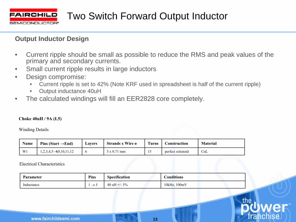
Two Switch Forward Output Inductor
Output Inductor Design
• Current ripple should be small as possible to reduce the RMS and peak values of the primary and secondary currents.
• Small current ripple results in large inductors• Design compromise:
• Current ripple is set to 42% (Note KRF used in spreadsheet is half of the current ripple)• Output inductance 40uH
• The calculated windings will fill an EER2828 core completely.
Choke 40uH / 9A (L5)
Winding Details
Name Pins (Start →End) Layers Strands x Wire ø Turns Construction Material
W1 1,2,3,4,5 →8,9,10,11,12 6 5 x 0.71 mm 15 perfect solenoid CuL
Electrical Characteristics
Parameter Pins Specification Conditions
Inductance 1 → 5 40 uH +/- 5% 10kHz, 100mV
14
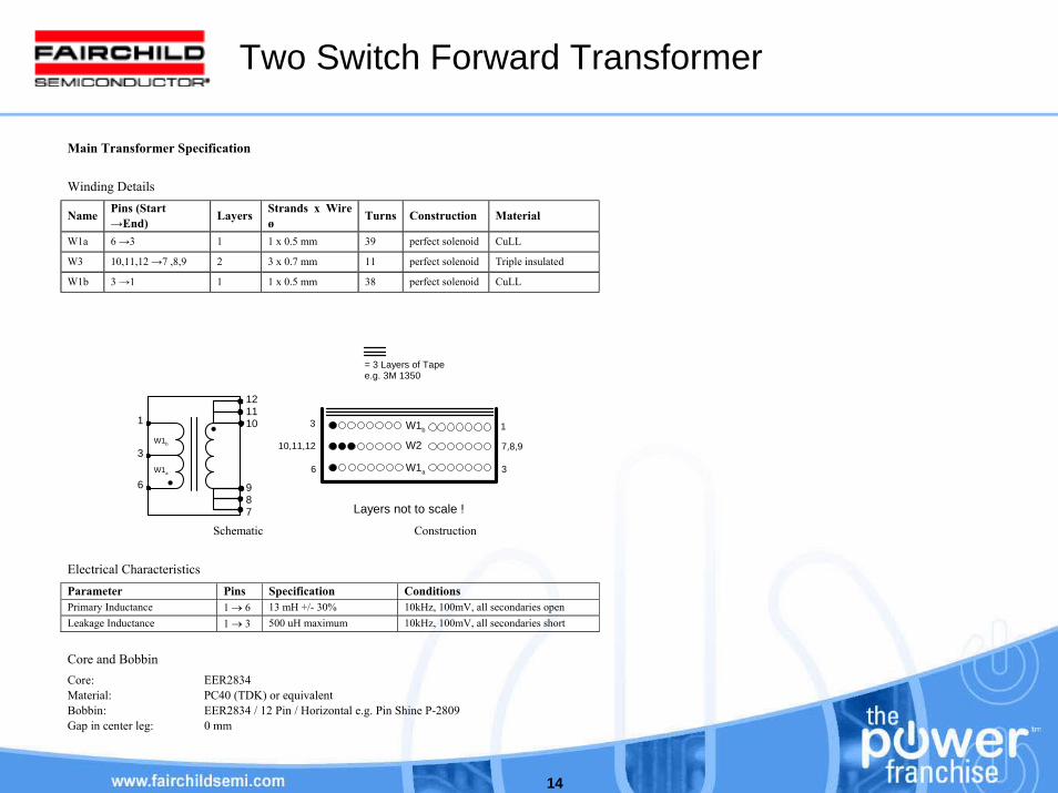
Two Switch Forward Transformer
Main Transformer Specification
Winding Details
Name Pins (Start →End) Layers Strands x Wire
ø Turns Construction Material
W1a 6 →3 1 1 x 0.5 mm 39 perfect solenoid CuLL
W3 10,11,12 →7 ,8,9 2 3 x 0.7 mm 11 perfect solenoid Triple insulated
W1b 3 →1 1 1 x 0.5 mm 38 perfect solenoid CuLL
6
1
Layers not to scale !
3W1a
W2
W1b
6 3
1
= 3 Layers of Tapee.g. 3M 1350
W1b
W1a
3
10,11,12 7,8,9
101112
789
Schematic Construction
Electrical Characteristics Parameter Pins Specification Conditions Primary Inductance 1 → 6 13 mH +/- 30% 10kHz, 100mV, all secondaries open Leakage Inductance 1 → 3 500 uH maximum 10kHz, 100mV, all secondaries short
Core and Bobbin Core: EER2834 Material: PC40 (TDK) or equivalent Bobbin: EER2834 / 12 Pin / Horizontal e.g. Pin Shine P-2809 Gap in center leg: 0 mm
15
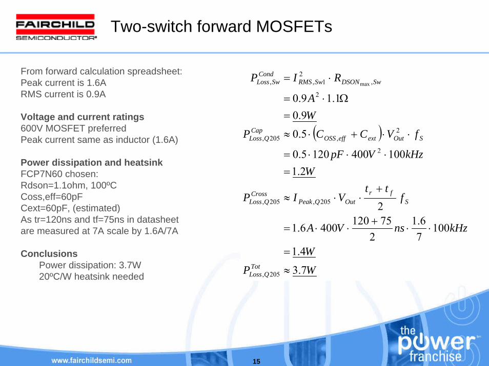
Two-switch forward MOSFETs
From forward calculation spreadsheet:Peak current is 1.6A RMS current is 0.9A
Voltage and current ratings600V MOSFET preferredPeak current same as inductor (1.6A)
Power dissipation and heatsinkFCP7N60 chosen:Rdson=1.1ohm, 100ºCCoss,eff=60pFCext=60pF, (estimated)As tr=120ns and tf=75ns in datasheetare measured at 7A scale by 1.6A/7A
ConclusionsPower dissipation: 3.7W20ºC/W heatsink needed
( )
WP
W
kHznsVA
ftt
VIP
WkHzVpF
fVCCP
WA
RIP
TotQLoss
Sfr
OutQPeakCross
QLoss
SOutexteffOSSCap
QLoss
SwDSONSwRMSCond
SwLoss
7.3
4.1
10076.1
2751204006.1
2
2.11004001205.0
5.0
9.01.19.0
205,
205,205,
2
2,205,
2
,2
1,, max
≈
=
⋅⋅+
⋅⋅=
+⋅⋅≈
=⋅⋅⋅=
⋅⋅+⋅≈
=Ω⋅=
⋅=
16
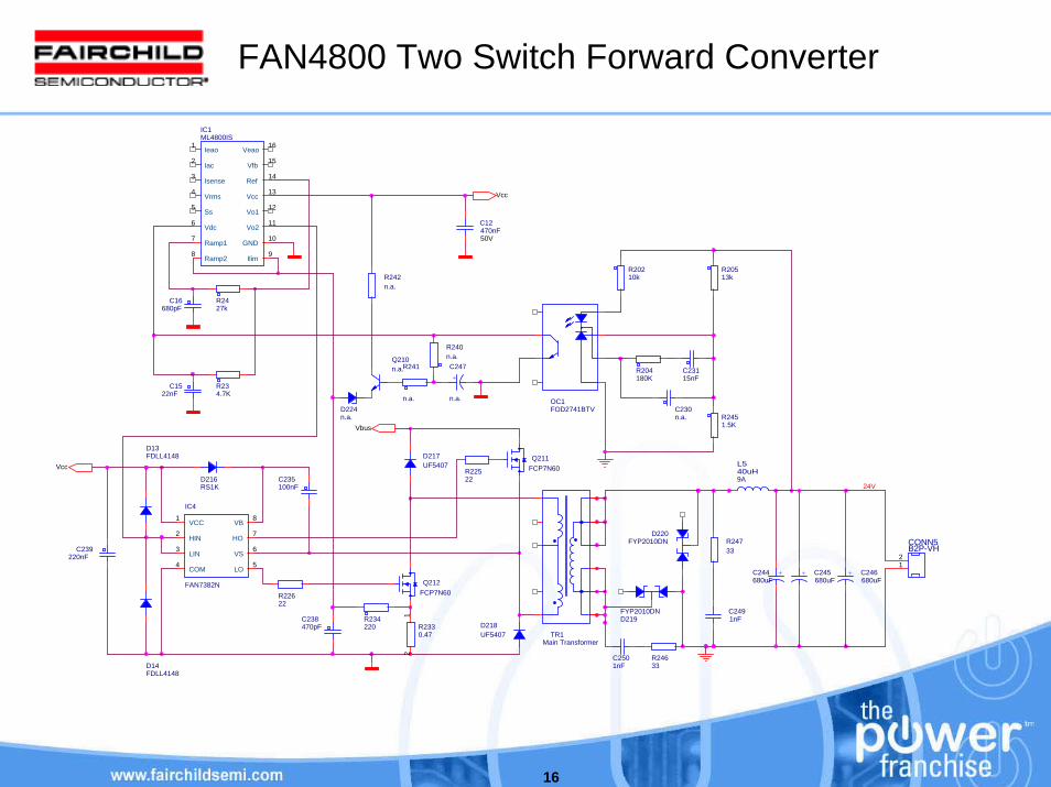
FAN4800 Two Switch Forward Converter
24V
R242n.a.
C2491nF
R24633
Q211FCP7N60
12
CONN5B2P-VH
R22522
R20513k
R20210k
C235100nF
R2451.5K
C1522nF
TR1Main Transformer
R241
n.a.
C16680pF
+
C247
n.a.1
2
R2330.47
R2427k
R240n.a.
D216RS1K
+ C246680uF
OC1FOD2741BTV
R234.7K
Ieao1
Iac2
Isense3
Vrms4
Ss5
Vdc6
Ramp17
Ramp28
Ilim9
GND10
Vo211
Vo112
Vcc13
Ref14
Vfb15
Veao16
IC1ML4800IS
R24733
D220FYP2010DN
R22622
D14FDLL4148
C23115nF
L540uH9A
D224n.a.
C238470pF
C239220nF
C2501nF
+ C245680uFQ212
FCP7N60
D217UF5407
Q210n.a.
+C244680uF
D218UF5407
D219FYP2010DN
C12470nF50V
D13FDLL4148
VCC1
HIN2
LIN3
COM4
LO5
VS6
HO7
VB8
IC4
FAN7382N
R204180K
R234220
C230n.a.
Vbus
Vcc
Vcc
17
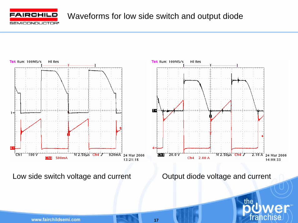
Waveforms for low side switch and output diode
Low side switch voltage and current Output diode voltage and current
18
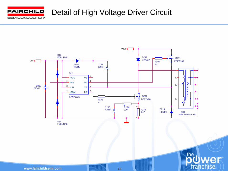
Detail of High Voltage Driver Circuit
Q211FCP7N60R225
22C235100nF
TR1Main Transformer
12
R2330.47
D216RS1K
R22622
D14FDLL4148
C238470pF
C239220nF
Q212FCP7N60
D217UF5407
D218UF5407
D13FDLL4148
VCC1
HIN2
LIN3
COM4
LO5
VS6
HO 7VB
8
IC4
FAN7382N
R234220
Vbus
Vcc
19
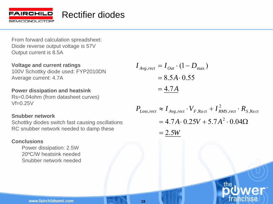
Rectifier diodes
From forward calculation spreadsheet:Diode reverse output voltage is 57VOutput current is 8.5A
Rs=0.04ohm (from datasheet curves)Vf=0.25V
Snubber networkSchottky diodes switch fast causing oscillationsRC snubber network needed to damp these
ConclusionsPower dissipation: 2.5W20ºC/W heatsink neededSnubber network needed
Voltage and current ratings100V Schottky diode used: FYP2010DN Average current: 4.7A
Power dissipation and heatsink AA
DII OutrectAvg
7.455.05.8
)1( max,
=⋅=
−⋅=
WAVA
RIVIP ctSrectRMSctFrectAvgrectLoss
5.204.07.525.07.4 2
Re,2
,Re,,,
=Ω⋅+⋅=
⋅+⋅≈
20
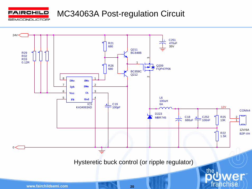
MC34063A Post-regulation Circuit
R26680
C252100nF
R32
Q212BC858C
Q211BC848B
12
CONN4
B2P-VH
1
2
3
45
6
7
8SWc
SWe
Ct
GndFB
Vcc
Ipk
DRc
IC5KA34063AD
+ C18680uF
R221.5K
C19100pF
L6100uH6A
1
23
Q209FQP47P06
R2513K
R29
D223MBR745
R21680
R330.12R
+ C251470uF35V
12V/6A
12V
24V
0
Hysteretic buck control (or ripple regulator)
21
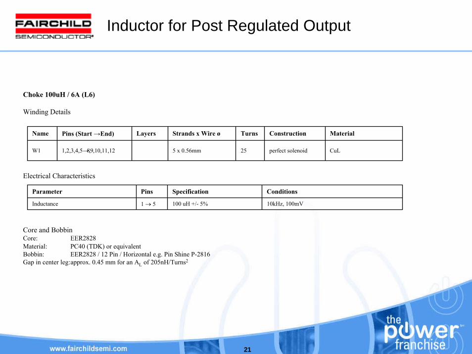
Inductor for Post Regulated Output
Choke 100uH / 6A (L6)
Winding Details
Name Pins (Start →End) Layers Strands x Wire ø Turns Construction Material
W1 1,2,3,4,5 →8,9,10,11,12 5 x 0.56mm 25 perfect solenoid CuL
Electrical Characteristics
Parameter Pins Specification Conditions
Inductance 1 → 5 100 uH +/- 5% 10kHz, 100mV
Core and BobbinCore: EER2828Material: PC40 (TDK) or equivalentBobbin: EER2828 / 12 Pin / Horizontal e.g. Pin Shine P-2816Gap in center leg:approx. 0.45 mm for an AL of 205nH/Turns2
22
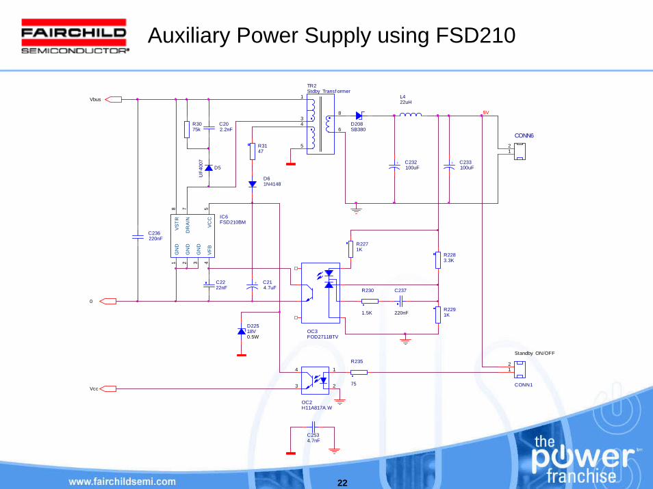
Auxiliary Power Supply using FSD210
D208SB380
C236220nF
OC3FOD2711BTV
R235
75
+ C214.7uF
1
23
4
OC2H11A817A.W
D61N4148
R2291K
1
34
5
6
8
TR2Stdby Transf ormer
C2222nF
R3147
R230
1.5K
D22518V0.5W
C237
220nF
+ C232100uF
R2271K
C202.2nF
12
CONN6
D5
UF
4007
R3075k
R2283.3K
C2534.7nF
VC
C5
DR
AIN
7V
ST
R8
GN
D1
GN
D2
GN
D3
VF
B4
IC6FSD210BM
12
CONN1
+ C233100uF
L422uH
Standby ON/OFF
5V
Vbus
0
Vcc
23
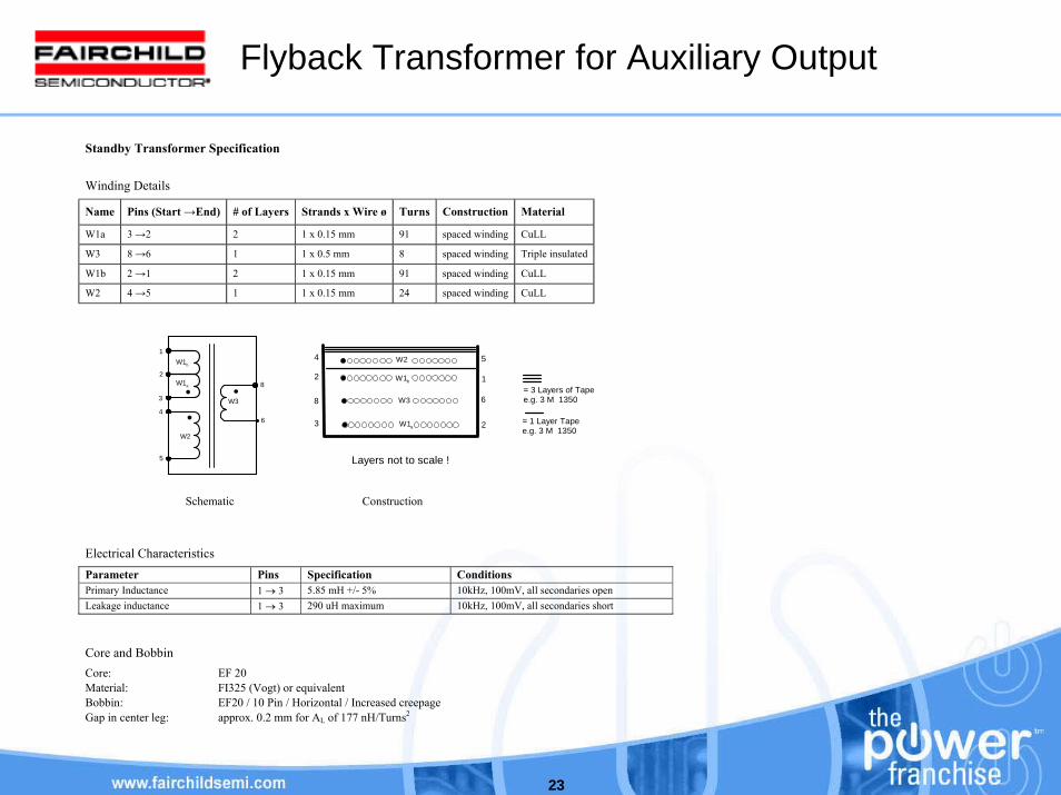
Flyback Transformer for Auxiliary Output
Standby Transformer Specification
Winding Details
Name Pins (Start →End) # of Layers Strands x Wire ø Turns Construction Material
W1a 3 →2 2 1 x 0.15 mm 91 spaced winding CuLL
W3 8 →6 1 1 x 0.5 mm 8 spaced winding Triple insulated
W1b 2 →1 2 1 x 0.15 mm 91 spaced winding CuLL
W2 4 →5 1 1 x 0.15 mm 24 spaced winding CuLL
W2
5
4
3
1
8
W3
2
W1b
W1a
6
= 3 Layers of Tapee.g. 3 M 1350
= 1 Layer Tapee.g. 3 M 1350
Layers not to scale !
W1a
W3
W1b
W2
3 2
1
4 5
8
2
6
Schematic Construction
Electrical Characteristics Parameter Pins Specification Conditions Primary Inductance 1 → 3 5.85 mH +/- 5% 10kHz, 100mV, all secondaries open Leakage inductance 1 → 3 290 uH maximum 10kHz, 100mV, all secondaries short
Core and Bobbin Core: EF 20 Material: FI325 (Vogt) or equivalent Bobbin: EF20 / 10 Pin / Horizontal / Increased creepage Gap in center leg: approx. 0.2 mm for AL of 177 nH/Turns2
24
Layout and Heatsink
• General Power Supply Layout Rules• the enclosed area of loops with high di/dt must be as small as possible• the copper area of nodes with high dv/dt must be as small as possible.• avoid common impedance coupling by using star connections to ground
• These rules conflict with other requirements• Heatsink construction at the edge of a board• Star connection of all ground lines would enlarge the PCB• Low cost solutions require single sided PCB’s which result in longer traces
• Compromise• Critical signals are routed to the shortest path• Less critical signals give way to the large ground plane which emulates star-like connection
• Heatsink• All devices except Q1 are connected to a simple heatsink made of
2mm aluminium bent into the form of a U• Q1 dissipates more power so needs an additional heatsink
25
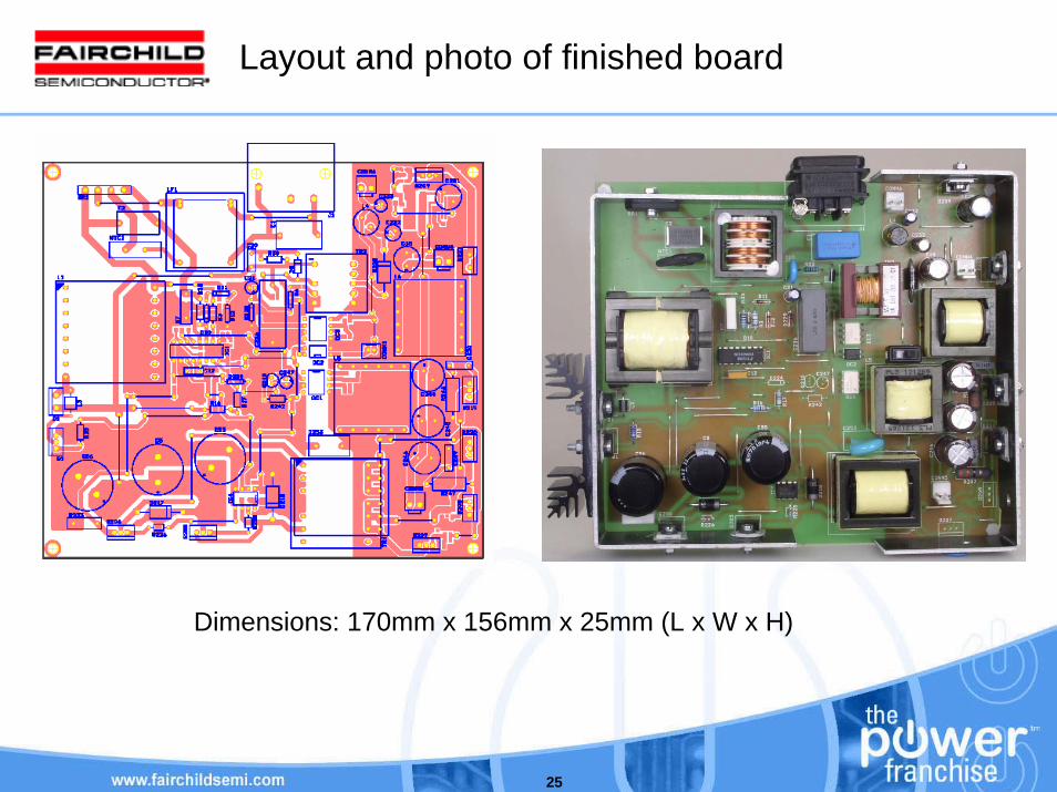
Layout and photo of finished board
Dimensions: 170mm x 156mm x 25mm (L x W x H)
26
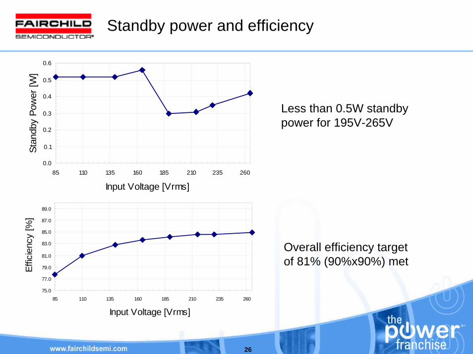
Standby power and efficiency
Less than 0.5W standbypower for 195V-265V
Overall efficiency targetof 81% (90%x90%) met
0.0
0.1
0.2
0.3
0.4
0.5
0.6
85 110 135 160 185 210 235 260
Input Voltage [Vrms]
Stan
dby
Pow
er [W
]
75.0
77.0
79.0
81.0
83.0
85.0
87.0
89.0
85 110 135 160 185 210 235 260
Input Voltage [Vrms]
Effic
ienc
y [%
]
27
Summary
Design Issues• System partitioning• Low profile boost inductor• PFC MOSFET dissipation• Using single switch forward tools to design two-switch
forward converters• Two-switch forward drive• Second output for a forward converter• Auxiliary power supply• Layout• Performance
![U-165 Reference Design: Isolated 50 Watt Flyback Converter ...Transformer Design [2] The transformer in a flyback converter is actually a coupled inductor with multiple windings. Trans-formers](https://img.pdfslide.net/doc/110x75/6067efcf513c1477013c4438/u-165-reference-design-isolated-50-watt-flyback-converter-transformer-design.jpg)