Embed Size (px)
Citation preview

McMaster UniversityDigitalCommons@McMaster
Open Access Dissertations and Theses Open Dissertations and Theses
4-1-2012
Detecting Radiation Pressure in Waveguides UsingMicroelectromechanical ResonatorsChristopher R P PopeMcMaster University, [email protected]
Follow this and additional works at: http://digitalcommons.mcmaster.ca/opendissertationsPart of the Nanoscience and Nanotechnology Commons
This Thesis is brought to you for free and open access by the Open Dissertations and Theses at DigitalCommons@McMaster. It has been accepted forinclusion in Open Access Dissertations and Theses by an authorized administrator of DigitalCommons@McMaster. For more information, pleasecontact [email protected].
Recommended CitationPope, Christopher R P, "Detecting Radiation Pressure in Waveguides Using Microelectromechanical Resonators" (2012). Open AccessDissertations and Theses. Paper 6592.

RADIATION PRESSURE IN WAVEGUIDE RESONATORS

DETECTING RADIATION PRESSURE IN WAVEGUIDES USINGMICROELECTROMECHANICAL RESONATORS
By CHRISTOPHER POPE, B.Sc
A Thesis Submitted to the School of Graduate Studies in Partial Fulfilmentof the Requirements for the Degree Master of Applied Science
McMaster University
c© Copyright by Christopher Pope, December 2011

McMaster University MASTER OF APPLIED SCIENCE (2011) Hamilton,Ontario (Engineering Physics)
TITLE: Detecting Radiation Pressure in Waveguides Using MicroelectromechanicalResonatorsAUTHOR: Christopher Pope, B.Sc. (University of Saskatchewan)SUPERVISOR: Dr. Rafael N. KleimanNUMBER OF PAGES: x, 84
ii

Abstract
The phenomenon of radiation pressure has fascinated scientists since it wasfirst proposed by Maxwell in the late 19th century. Numerous experimentsinvolving optical forces have been carried out, however the optical force actingon a curved waveguide does not appear to have been previously investigated.An experiment to measure the force acting on a waveguide due to the opticalpower it contains is proposed here. This experiment takes advantage of thesensitivity of MicroElectroMechanical Systems (MEMS) and the performanceof silicon integrated optics in a single hybrid device.
Devices are fabricated from silicon-on-insulator (SOI) wafers using con-ventional micromachining techniques. Anisotropic alkali etches are used toproduce smooth vertical side-walls for a mechanical structure and a rib waveg-uide. An analysis of the electrical systems and measurement techniques isprovided. Using these techniques, the resonant operation of the devices isdemonstrated by means of capacitive actuation and sensing. The applicationof this system to the measurement of radiation pressure is discussed.
iii

Acknowledgements
I wish to thank my supervisor, Dr. Rafael N. Kleiman for inspiring this project,and for his helpful insight and guidance throughout this project. I am gratefulto Abhishaik Rampal for the extensive advice, assistance and support providedduring this endeavor. I am thankful for the training and assistance providedby Dr. Zhilin Peng and Doris Stevanovic from the Centre for Emerging DeviceTechnologies, which made fabrication possible. I wish thank my colleages Dr.Sri Priya Sundararajan, Matthew Minnick, Sarah Selesnic and Nikolaus Jewellfor helpful discussions and advice during the course of the project. Finally, Iwould like to thank my parents for their continued support in this endeavor.
iv
Contents
List of Figures . . . . . . . . . . . . . . . . . . . . . . . . . . . . . . viiList of Tables . . . . . . . . . . . . . . . . . . . . . . . . . . . . . . viiiNotation . . . . . . . . . . . . . . . . . . . . . . . . . . . . . . . . . ixAbbreviations . . . . . . . . . . . . . . . . . . . . . . . . . . . . . . x
1 Introduction 11.1 Radiation Pressure . . . . . . . . . . . . . . . . . . . . . . . . 11.2 MEMS . . . . . . . . . . . . . . . . . . . . . . . . . . . . . . . 21.3 Thesis Overview . . . . . . . . . . . . . . . . . . . . . . . . . . 3
2 Theory 52.1 Abraham and Minkowski . . . . . . . . . . . . . . . . . . . . . 52.2 Optical Forces . . . . . . . . . . . . . . . . . . . . . . . . . . . 132.3 Elasticity . . . . . . . . . . . . . . . . . . . . . . . . . . . . . 182.4 Waveguides . . . . . . . . . . . . . . . . . . . . . . . . . . . . 232.5 Electromechanical systems . . . . . . . . . . . . . . . . . . . . 25
3 Design and Fabrication 343.1 Fabrication Techniques . . . . . . . . . . . . . . . . . . . . . . 343.2 Device Design . . . . . . . . . . . . . . . . . . . . . . . . . . . 363.3 Fabrication . . . . . . . . . . . . . . . . . . . . . . . . . . . . 383.4 Fabrication challenges . . . . . . . . . . . . . . . . . . . . . . 44
4 Experiment 494.1 Electrical Experiment . . . . . . . . . . . . . . . . . . . . . . . 494.2 Resonance Measurements . . . . . . . . . . . . . . . . . . . . . 594.3 Effective Spring Constant . . . . . . . . . . . . . . . . . . . . 644.4 Optical Experiment . . . . . . . . . . . . . . . . . . . . . . . . 71
5 Conclusion 735.1 Summary . . . . . . . . . . . . . . . . . . . . . . . . . . . . . 735.2 Future Work . . . . . . . . . . . . . . . . . . . . . . . . . . . . 74
References 76
v

List of Figures
1.1 Fabricated device . . . . . . . . . . . . . . . . . . . . . . . . . 4
2.1 Abraham example . . . . . . . . . . . . . . . . . . . . . . . . . 92.2 Minkowski example . . . . . . . . . . . . . . . . . . . . . . . . 102.3 Photon interaction . . . . . . . . . . . . . . . . . . . . . . . . 152.4 Beam bending . . . . . . . . . . . . . . . . . . . . . . . . . . . 212.5 Mode shape of a bridge . . . . . . . . . . . . . . . . . . . . . . 232.6 Mode shape of a cantilever . . . . . . . . . . . . . . . . . . . . 242.7 SOI rib waveguide . . . . . . . . . . . . . . . . . . . . . . . . 262.8 Resonance plot . . . . . . . . . . . . . . . . . . . . . . . . . . 292.9 Pull-in voltage . . . . . . . . . . . . . . . . . . . . . . . . . . . 32
3.1 Anisotropically etched bridge . . . . . . . . . . . . . . . . . . 363.2 Rendering of device . . . . . . . . . . . . . . . . . . . . . . . . 373.3 Chip layout . . . . . . . . . . . . . . . . . . . . . . . . . . . . 393.4 Photolithography masks . . . . . . . . . . . . . . . . . . . . . 403.5 Process cross-sections . . . . . . . . . . . . . . . . . . . . . . . 413.6 Fabricated device . . . . . . . . . . . . . . . . . . . . . . . . . 433.7 Released bridge . . . . . . . . . . . . . . . . . . . . . . . . . . 453.8 Cleaved edge . . . . . . . . . . . . . . . . . . . . . . . . . . . 463.9 Curved bridge . . . . . . . . . . . . . . . . . . . . . . . . . . . 47
4.1 Electrode schematic . . . . . . . . . . . . . . . . . . . . . . . . 504.2 PCB design . . . . . . . . . . . . . . . . . . . . . . . . . . . . 514.3 PCB with device . . . . . . . . . . . . . . . . . . . . . . . . . 524.4 Three-terminal schematic . . . . . . . . . . . . . . . . . . . . . 534.5 Measurement schematic . . . . . . . . . . . . . . . . . . . . . 564.6 System block diagram . . . . . . . . . . . . . . . . . . . . . . 574.7 Destroyed device . . . . . . . . . . . . . . . . . . . . . . . . . 584.8 Resonance plot - 1000 µm device . . . . . . . . . . . . . . . . . 594.9 Resonance plot - 600 µm device . . . . . . . . . . . . . . . . . 604.10 Resonance stability . . . . . . . . . . . . . . . . . . . . . . . . 624.11 Effect of balancing . . . . . . . . . . . . . . . . . . . . . . . . 634.12 Overdriven response . . . . . . . . . . . . . . . . . . . . . . . 64
vi

4.13 Resonance shift - 600 µm . . . . . . . . . . . . . . . . . . . . . 654.14 Frequency vs Bias - 600 µm . . . . . . . . . . . . . . . . . . . 664.15 Response vs Bias - 600 µm . . . . . . . . . . . . . . . . . . . . 674.16 Resonance shift - 1 mm . . . . . . . . . . . . . . . . . . . . . . 684.17 Frequency vs Bias - 1 mm . . . . . . . . . . . . . . . . . . . . 694.18 Response vs Bias - 1 mm . . . . . . . . . . . . . . . . . . . . . 704.19 Separate bias circuit . . . . . . . . . . . . . . . . . . . . . . . 704.20 Optical experiment setup . . . . . . . . . . . . . . . . . . . . . 72
vii

List of Tables
2.1 Maxwell’s Equations . . . . . . . . . . . . . . . . . . . . . . . 72.2 Expressions for electromagnetic momentum . . . . . . . . . . . 8
3.1 Micromachining etches . . . . . . . . . . . . . . . . . . . . . . 35
4.1 Calculated device capacitances . . . . . . . . . . . . . . . . . . 544.2 Measured device capacitance . . . . . . . . . . . . . . . . . . . 554.3 Measured and calculated resonant frequencies . . . . . . . . . 61
viii

Notation
c Speed of light in a vacuum~D Dielectric fieldE Young’s modulus~E Electric fieldf Frequency, force density~g Momentum densityh Planck’s constant~ Reduced Planck’s constant h/2πk Spring constant, stiffnessP PressureP Powerε Dielectric constant, Strainε0 Electric constant (permittivity of free space)µ0 Magnetic constant (permeability of free space)λ Wavelengthω Angular frequency
ix

Abbreviations
AC Alternating CurrentBHF Buffered HFCVD Chemical Vapour DepositionCPD Critical Point DryingDIP Dual Inline PinDC Direct Current
DUT Device Under TestEM ElectromagneticHF Hydrogen Fluoride, Hydrofluoric Acid
IPA Isopropyl AlcoholSNR Signal to Noise RatioSOI Silicon-on-Insulator
PCB Printed Circuit Board
x

Chapter 1
Introduction
1.1 Radiation Pressure
Radiation pressure has been a subject of interest since the pressure exertedby light on a surface was first calculated by Maxwell in 1873 [1, 2]. The firstmeasurements of the radiation pressure force were made by Nichols and Hull[3, 4] and independently by Lebedew [5] in 1901.
An interesting use of radiation pressure forces is in optical tweezers, firstdemonstrated by Ashkin in 1969 [6, 7]. Transparent particles can be trapped atthe focus of a laser beam, as in a potential well. Light refracted by the particleexperiences a change in momentum which generates an optical restoring force.These techniques have been extended from inert spheres [8] to living cells [9]and to the trapping and cooling of atoms [10, 11], opening up opportunitiesfor new science [12].
Another potential application of radiation pressure is spacecraft propulsionin the form of solar sails [13]. A thin membrane with a large surface area cancapture sufficient energy to accelerate a spacecraft while requiring no reactionmass. Solar sails have been employed in the Japanese IKAROS and NASA’sNanoSail-D missions [14, 15], and further missions are planned. Solar sails arealso popular topics in science fiction where they were popularized by storiessuch as Arthur C. Clarke’s Sunjammer [16].
The momentum carried by a photon or electromagnetic wave propagatingin free space is well understood, but the momentum of light in a medium hasbeen the subject of debate. The first expression was proposed by Minkowski[17, 18] who calculated that the momentum density of an EM wave propa-gating in a dielectric medium should increase relative to its free-space valueby a factor n equal to the refractive index of the medium. Abraham [19, 20]calculated a different expression for the momentum density, suggesting thatit should instead decrease by a factor of n. This is the origin of what isknow as the Abraham-Minkowski controversy, which has been discussed by a
1

Masters Thesis - Christopher Pope McMaster University - Eng. Physics
number of authors for the last century. Recent works have claimed to resolvethis controversy theoretically [21, 22, 23] and experimentally [24], though theexperimental results are disputed [25, 26].
1.2 MEMS
Several terms, including microsystems and microelectromechanical systems(MEMS), are used to describe the growing number of microscale devices cou-pling mechanical structures to electrical, optical, thermal and other physicaleffects [27]. An early call to take advantage of the opportunities offered byminiturization was made by Richard Feynman in his classic 1959 talk There’sPlenty of Room at the Bottom [28]. Industrial applications beginning in the1970s included pressure sensors, print heads, inertial sensors and optical de-vices with a variety of other possible applications under development [27, 29].
Although not usually classified as a MEMS device, and preceding the ICindustry by several decades, the most common micromechanical device is prob-ably the crystal oscillator. First developed around 1920 [30] they allowed forsignificantly better time-keeping than mechanical mechanisms. Significant ef-fort has been invested in improving the technology due to the value of accuratefrequency standards in radio receivers. In modern digital electronics crystaloscillators are commonly used to provide clock references for digital logic,timekeeping and wireless communication systems.
The first reported use of a silicon-based electromechanical system was theresonant gate transistor in 1965 [31, 32] which combines a conventional metal-oxide-semiconductor (MOS) transistor with a moving beam which forms thegate. The original experiments demonstrated a band-pass behavior at the me-chanical resonant frequency of the beam, foreshadowing later radio-frequencyMEMS applications [33]. The integration with MOS circuitry and fabricationtechniques demonstrated some of the advantages of silicon over other compet-ing materials.
Silicon is a good material for MEMS applications due to material proper-ties and synergies with integrated circuit (IC) processing methods [34]. Single-crystal silicon is a nearly perfect Hookesian material with tensile strength andYoung’s modulus comparable to steel, allowing the construction of durabledevices. Many manufacturing techniques developed for CMOS IC processinghave been adapted to the production of microsystems including photolithog-raphy, wet and dry etching and chemical vapour deposition (CVD) [29]. Theavailability of processing equipment, raw materials and expertise reduces costsand makes silicon a more attractive material. The possibility of integratingcircuitry with silicon-based mechanical devices is another advantage.
An early and ongoing area of interest has been the integration of optical andMEMS devices. Early examples included light modulators [35] and steerable
2

Masters Thesis - Christopher Pope McMaster University - Eng. Physics
mirrors [36]. One of the more wide-spread optical MEMS devices is the DigitalLight Processor (DLP), used for video projection [37] and a variety of otherapplications. Recent examples have included attenuators based on movingwaveguides [38] and optical switches [39, 40].
Optical actuation of microsystems has been an area of interest in recentyears. An early example demonstrated the force of a laser beam on a MEMSmirror, and used this force to excite the mechanical resonance of the structure[41]. Recent works have proposed the existence of optical forces due to evanes-cent fields from a dielectric waveguide [42]. This effect has been demonstratedin nanoscale silicon waveguides [43, 44] and in a whispering gallery resonator[45].
MEMS devices have been used in research environments to measure verysmall forces. One example is a force transducer used to measure the contrac-tion force exerted by a single heart cell [46]. Forces in the µN range weresuccessfully measured.
1.3 Thesis Overview
This project proposes to measure radiation pressure forces in a novel geometryby harnessing the flexibility of MEMS fabrication and sensing techniques. Asection of a silicon waveguide is fabricated as a double-clamped beam whichforms a mechanical resonator. As the beam bends the light propagating inthe waveguide exerts a restoring force on the beam. This force is an opticalstiffness which adds to the mechanical spring constant of the structure. Whenthe mechanical structure is driven in resonance the optical stiffness can bedetected as a change in resonance frequency with changing optical power.Using a resonant structure allows for an increased sensitivity by filtering outDC effects.
The design, fabrication and operation of devices which can carry out thisexperiment is described in this thesis. Devices are fabricated from SOI wafersby means of anisotropic etching, and the mechanical structures have been suc-cessfully released. An example of a fabricated device is shown in Figure 1.1.The techniques necessary for capacitive actuation and detection of the MEMSresonator are discussed. The resonant behavior of the device is investigatedand an electrostatic softening of the structure is demonstrated by observing adecrease in the resonant frequency. The theory of optical-mechanical interac-tion is discussed, along with the proposed optical experiment.
3

Masters Thesis - Christopher Pope McMaster University - Eng. Physics
Figure 1.1: SEM micrograph of a fabricated device. The bridge length is 400microns.
4

Chapter 2
Theory
2.1 Abraham and Minkowski
2.1.1 Energy and Momentum
Kinetic energy and momentum are related classically by the expression
E =p2
2m(2.1)
which is valid for slow-moving massive particles. Special relativity providesthe alternate expression [47]
E = c√p2 +m2c2 (2.2)
which is valid for all particles, including photons where it reduces to
E = pc (2.3)
or alternately
p =E
c=hf
c(2.4)
The de Broglie wavelength of a particle is related to its momentum by
λ =h
p(2.5)
This expressions is valid for both massive and massless particles. For a photonthis reduces to
λ =c
f(2.6)
5

Masters Thesis - Christopher Pope McMaster University - Eng. Physics
While the above analysis is based on the particle picture of light it is equallyvalid to consider the case of a traveling electromagnetic wave. If the wavecaries an energy flux S (energy per unit time per unit area) in the directionof propagation then it has an energy density
U =S
c(2.7)
in the steady state, where c is the speed of propagation. Using the relationfrom (2.4) the momentum density of the wave is
g =S
c2(2.8)
This is the natural form when dealing with wave problems, such as light con-fined in a waveguide.
2.1.2 Two Approaches
Electromagnetic problems are typically analyzed through the use of Maxwell’sequations in some form. Depending on the nature of the problem these equa-tions can be constructed in a number of forms and popularly in two choices offield variables [48]. The first choice is in terms of the electric field ~E and the
magnetic field ~B,1 sometimes referred to as the microscopic fields. The physicsdescribed by Maxwell’s equations in this form is universal and is the basis forunderstanding the electromagnetic behavior of matter. For this reason theyare referred to as the microscopic fields.
In the presence of a medium which experiences polarization or magnetiza-tion it is sometimes convenient to abstract the material properties into simpleconstants. Maxwell’s equations may then be constructed in terms of the di-electric field ~D and the magnetizing field ~H, also called the macroscopic fieldvariables. These fields depend only on the free charge and current respectivelyand therefore may be more convenient as it is the free parameters that aretypically under experimental control.2
The photon momentum given in Equation (2.4) is valid for the free-spaceor microscopic case. This corresponds to a momentum density
~g =~S
c2(2.10)
1The choice of names for the ~B and ~H fields varies, with some authors preferring to call~H the magnetic field.
2In fact, it is more usual to control the electric potential V rather than the free charge,making ~E and ~H the natural variables in some engineering applications.
6

Masters Thesis - Christopher Pope McMaster University - Eng. Physics
Microscopic Macroscopic
∇ · ~E =ρ
ε0∇ · ~D = ρf (2.9a)
∇× ~E = −d~B
dt∇× ~D = −d
~B
dt(2.9b)
∇ · ~B = 0 ∇ · ~B = 0 (2.9c)
∇× ~B = µ0∇ · ~J + µ0ε0d ~E
dt∇× ~H = ∇ · ~Jf +
d ~D
dt(2.9d)
Table 2.1: Maxwell’s equations, in both microscopic and macroscopicforms.[48]
where the Poynting vector ~S is the energy flux carried by the fields.[49] ThePoynting vector is given by
~S = ~E × ~H (2.11)
For electromagnetic waves it is more convenient to use the definition
~S =1
2Re[ ~E × ~H∗] (2.12)
which is known as the time-averaged Poynting vector, representing the averagerate of energy transfer, or power, carried by the wave. A simpler form is theratio of the power carried by a wave to the area that wave passes through
S =P
A(2.13)
which is the form most useful when considering EM waves in a waveguide.In the case of a photon traveling in a medium the situation is more in-
teresting. Two forms for the photon momentum have been advanced, bothsupported by theory and experiment. The first formulation, proposed by Her-mann Minkowski in 1908 [17, 18] suggests an increase of the momentum ina medium. The second form, proposed by Max Abraham in 1909 [19, 20]predicts a decrease in the momentum on entering a medium. In a dielectricmedium with a refractive index n these two forms differ by a factor of n2. Theexpressions for electromagnetic momentum are summarized in Table 2.2. Anumber of arguments have been made by various authors for one form or theother. An example from each side is presented here, along with an overviewof relevant experiments and the current state of the controversy. Extensiveoverviews of the literature can be found in references[50, 51, 21].
7
Masters Thesis - Christopher Pope McMaster University - Eng. Physics
Photon Momentum Momentum Density Interpretation
Maxwell p =hf
c~g =
~S
c2Free-space
Minkowski p =nhf
c~g =
~E × ~H
c2Canonical
Abraham p =hf
nc~g = ~D × ~B Kinetic
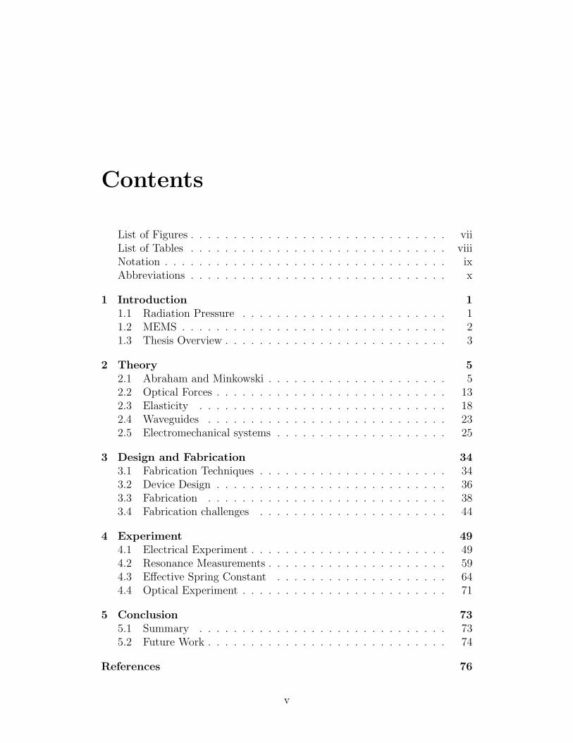
Table 2.2: Summary of the three expressions for electromagnetic momentum,in both the single-photon and momentum density forms.
2.1.3 Abraham
Abraham’s form for the electromagnetic momentum appears natural from amechanical point of view. If the photon behaved like a massive particle thenslowing as it entered a medium would naturally reduce its momentum. Theargument presented here follows the example of Barnett and Loudon [21] whopresent a simplification of the work of Balazs [52].
The Abraham momentum may be derived by considering the case of aphoton entering a transparent block, as illustrated in Figure 2.1. The blockhas mass M and is initially at rest while the photon is moving with a velocityc and an energy hf . Upon entering the block the photon slows to a speedc/n and travels the block length L in a time nL/c. Had the photon passedby the block it would have traveled a distance nL in this time, a differenceof L(n− 1). Relativity requires that the center of mass-energy of an isolatedsystem experience uniform motion. Thus, the distance traveled by the centerof mass-energy must be the same in both cases
0Mc2 + nLhf = ∆xMc2 + Lhf (2.14)
∆xMc2 = (n− 1)Lhf (2.15)
∆x = L(n− 1)hf
Mc2(2.16)
requiring the block to be displaced by a distance ∆x.3 Conservation of mo-
3This ignores the effect of the motion of the block on the motion of the photon which isvalid for ∆x L or hf Mc2
8

Masters Thesis - Christopher Pope McMaster University - Eng. Physics
mentum then gives
hf
c= pAbr +Mv (2.17)
pAbr =hf
c−M
[L(n− 1)
hf
Mc2
]c
nL(2.18)
pAbr =hf
nc(2.19)
where pAbr is the photon momentum. Thus, the photon momentum is reducedupon entering the medium and transfers a fraction (n−1)/n of its momentumto the medium.
M
L
hf
Figure 2.1: Diagram illustrating the argument for the Abraham form of theelectromagnetic momentum based on the uniform motion of the center of mass-energy.
2.1.4 Minkowski
Minkowski’s momentum appears natural when one considers the de Broglierelation p = h/λ relating momentum to wavelength. If a photon slows as itenters a medium then its wavelength must also shrink, given that its frequencyis constant. An analytical approach based on this change in wavelength is givenhere, again following Barnett and Loudon[21] based on the work of Padgett[53].
A collimated light beam incident on a slit of width ∆x undergoes diffractionand spreads to an angle
θ =λ
∆x(2.20)
9

Masters Thesis - Christopher Pope McMaster University - Eng. Physics
as shown in Figure 2.2. This angle can be approximated as the ratio of theaxial to transverse momentum
θ ≈ ∆pxpz
(2.21)
for small divergences. In this case the axial momentum pz is approximatelyequal to the incident momentum p0. The uncertainty principle
∆x∆p ≤ ~ (2.22)
allows us to rewrite (2.21) as
θ =~
∆x p0
(2.23)
pz
Δpx
Δx
p0
Figure 2.2: Diagram illustrating the argument for the Minkowski form of theelectromagnetic momentum based on diffraction and the uncertainty principle.
If the entire experiment is then immersed in a dielectric liquid with refrac-tive index n the wavelength of the incident light is reduced by a factor of n.By Equation (2.20) the diffraction angle must also be reduced to
θ =~
∆xnp0
(2.24)
which gives the Minkowski momentum as
pMin =n~ωc
(2.25)
Thus, the photon momentum increases in the medium, representing the addi-tional momentum being carried by the polarization of the medium.
10
Masters Thesis - Christopher Pope McMaster University - Eng. Physics
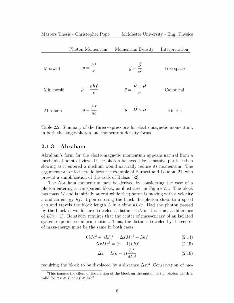
2.1.5 Selected experiments
In addition to the work of Nichols and Hull in 1901 [3, 4], a number of otherexperiments have been performed both to measure radiation pressure and inan attempt to resolve the Abraham-Minkowski controversy. The key challengein measuring radiation pressure is the magnitude of the force involved, as evenone watt of optical power produces a force of only 3 nN when absorbed. Thisplaces stringent requirements on experimental design, with the first work usinga torsion balance under high vacuum. A second and closely related challengeis proving that the observed effect is actually due to radiation pressure and notsome other mechanism, typically thermally driven. The Crooke’s radiometer,now a popular novelty item, consists of rotating vanes, dark on one side andreflective on the other, contained in a partially evacuated bulb. While theradiometer was originally believed to derive its motion from radiation pressureforces, in actuality the vanes rotate due to thermal gradients. Unequal heatingof the two sides of the vane causes air currents in an imperfect vacuum[54],a fact that can be readily proven simply by completely evacuating the bulb.4
Experimental design therefore must take into account thermal effects, typicallyby using high-reflectivity mirrors.
Photons also carry angular momentum of magnitude h, and a measurementof the angular momentum transfer required to change the polarization of alight beam was made in 1936 by Beth [55]. A light beam was passed througha quarter wave plate suspended from a torsion balance in vacuum and theresulting rotation was used to determine the force and thus the momentumchange.
The Jones-Richardson experiment, performed first in 1954 measured therecoil force on a mirror in a dielectric liquid[56] and found a result that sup-ported the Minkowski momentum. Significant improvements were made byJones and Leslie in 1977 [57], including the use of a high-reflectance dielectricmirror to reduce convection currents. The authors of the 1977 paper claimthat the radiation pressure force increases linearly with the phase refractiveindex, to an accuracy of 0.05 %.
An alternate measurement was performed by Ashkin and Dziedzic in 1973which measured the force on a liquid surface due to a laser beam exiting themedium [58]. An outward curvature of the surface was observed, consistentwith the Minkowski form, using a pulsed laser with a 4 kW peak power.
An experiment performed in 2002 by Graebner et al. [41] examined themotion of a MEMS mirror in response to the force exerted by an incidentlaser beam. An optical power of 3 mW was used to generate deflections on the
4In fact, simple observation shows that the net force on the vane is directed towards thedark, or less reflective side. This side absorbs more energy, but as can be readily calculated,the radiation pressure force is greatest on the reflective surface. Quite simply, the Crooke’sradiometer turns in the wrong direction for the motion to be due to radiation pressure.
11

Masters Thesis - Christopher Pope McMaster University - Eng. Physics
nm scale (measured using an interferometer), giving agreement within 30 %of the theory. Despite a mirror reflectivity of only 95 %, the authors madeno attempt to characterize the thermal effects on the system, relying on theagreement with theory as proof of the effect.
In 2008, She et al. observed the recoil force due to light leaving the end-face of a silica nanofiber [24] and reported a result which favors the Abrahamform. The fiber diameter of only 450 nm leads to a very soft structure and lightcoupled into it leads to an observable deflection. The authors’ conclusions are,however, disputed [25, 26].
Lui et al. have demonstrated a nanoscale plasmonic motor which harnessesthe angular momentum of light to rotate a silica disk [59]. The authors re-port a torque of 140 pN from an linearly polarized beam with an intensity of1 mW/µm2. Further, by changing the wavelength of the optical drive beamdifferent resonances could be excited in the structure allowing the direction ofthe torque, and thus the rotation, to be reversed. This effect opens anotheravenue for the optical actuation of microstructures.
The primary challenge in making measurements of optical momentum is theextremely small magnitude of the resulting force. This means that not onlymust the experiment be very sensitive, but it must also be isolated againstoutside perturbations or spurious responses. A significant concern is avoidingspurious responses due to thermal effects, which may be significant. Themechanical power transfered to a system is
Pmech =dEmechdt
=d
dt
p2mech
2m=pmechm
dpmechdt
(2.26)
Using the optical force F = Popt/c this becomes
Pmech =pmechPopt
mc(2.27)
The thermal power transfered to the system is simply
Ptherm = APopt (2.28)
where A is the total optical absorption in the beam path. For a mirror A equalsone minus the reflection coefficient, or about 1 % for typical metal mirrors.
Due to this issue, experiments attempting to measure optical forces musttake care to demonstrate that optical momentum is the cause of the observedforce, and not thermal effects. Techniques have included decreasing absorptionusing dielectric mirrors [57], high vacuum to prevent convection currents [3]and thermal time constants longer than the optical response frequency.
12

Masters Thesis - Christopher Pope McMaster University - Eng. Physics
2.1.6 Resolution
The Abraham-Minkowski controversy has been a subject of debate for the lastcentury due to the simple yet fundamental nature of the question. Experimen-tal resolution has been difficult, owing both to the small forces involved andthe apparently contradictory results. Recently a number of publications haveoffered5 a resolution to this controversy which accepts both forms, provided acorrect analysis is followed. [21, 22, 23] A simple summary might suggest thatthe Abraham form represents the Kinetic momentum of the photon while theMinkowski form represents the Canonical momentum.
The arguments presented above for the Abraham momentum are based onthe conservation of kinetic momentum and the motion of mass-energy. Thesemechanical arguments give the correct result when considering the force dueto light entering or leaving the medium and in other cases where the kineticmomentum is involved.
The canonical or Minkowski momentum arises in cases where the momen-tum is quantum in nature and satisfies the canonical commutation relation[x, p] = i~. This implies that the momentum is given by the momentumoperator p = −i~∇. Alternately, this is the correct approach where the wave-length is the fundamental property and momentum is given by p = h/λ andthe wavelength in the medium must be used.
2.2 Optical Forces
2.2.1 Derivation of radiation pressure
From (2.4), photons carry a momentum with magnitude
p =E
c=hf
c(2.29)
proportional to their energy. Should a photon with this momentum encountera reflecting surface, conservation of momentum gives6
pγi + pRi = pγf + pRf (2.30)
hf
c+ 0 = −hf
c+ ∆pR (2.31)
where pγ and pR are the momenta of the photon and the reflector before andafter the interaction. Thus the momentum change experienced by the reflector
5Or boldly claimed as in [22, 23]6Assuming a perpendicular angle of incidence
13

Masters Thesis - Christopher Pope McMaster University - Eng. Physics
is7
∆pR = 2hf
c= 2pγ (2.32)
Force on an object is equal to its change in momentum with time
~F =d~p
dt(2.33)
from Newton’s second law. In the case of a single photon the interaction timedt is not clear, but in the more practical (and therefore more interesting) caseof many photons arriving at a constant rate this becomes
F = 2d
dt
E
c(2.34)
= 2P
c(2.35)
which is a force proportional to the power incident on the reflecting surface.It is traditional to consider the pressure on a surface
P = 2P
cA= 2
S
c(2.36)
where A is the surface area receiving the force and S is the time-averagedPoynting vector.
If, instead of being reflected the photon is simply deflected by an angle θdue to its interaction with some structure, momentum conservation gives
~pγf = (p0 cos θ, p0 sin θ) (2.37)
∆~pi = (p0(1− cos θ),−p0 sin θ) (2.38)
for the interaction shown in Figure 2.3. It is interesting to note that thisinteraction is essentially a ‘black box’ and nothing need be assumed aboutthe nature of this interaction. If there are many photons passing into theinteraction at a constant rate then the above approach may be repeated, givinga force
~F =P
c(1− cos θ,− sin θ) (2.39)
on the structure with which the photons are interacting. The scalar magnitudeof this force is
‖F‖ = 2P
csin
θ
2(2.40)
which reduces to the form in Equation (2.35) for θ = π/2.
7An absorbing surface experiences half this momentum change as the final momentumof the photon in that case is zero.
14

Masters Thesis - Christopher Pope McMaster University - Eng. Physics
p0
θ
Δp
pf
x
y
Figure 2.3: Diagram illustrating the scattering of a photon from an arbitraryinteraction. The change in momentum of the interacting object is ∆~p = −(~pf−~p0).
2.2.2 Forces on waveguides
The optical force acting on a waveguide may be understood by considering thecase of a particle constrained to move along a curved path. If the particle hassome initial momentum ~p0 then by Newton’s second law it must experience aforce
~F =d~p
dt(2.41)
to keep it on that path. If the movement along the path is frictionless it isonly the direction of the momentum vector that changes, not the magnitude.At any point along the path the particle is traveling in a direction tangentto the path. If the path is described by a function ~u(x) then the momentumvector can be written
~p = p0d~u
dx(2.42)
and the force is thus
~F =d
dt
(p0du
dx
)(2.43)
= p0d
dx
(du
dx
)dx
dt(2.44)
= p0cd2~u
dx2(2.45)
15

Masters Thesis - Christopher Pope McMaster University - Eng. Physics
where c is the speed at which the particle travels along the path.The above derivation makes no assumptions about the nature of the par-
ticle and Newton’s second law is used in the relativistic form. Therefore, theconclusion in Equation (2.45) is valid for the case of a photon confined in awaveguide. By Newton’s third law the waveguide experiences an equal andopposite force, which acts to oppose the curvature. This force is proportionalto the curvature of the waveguide and represents an optical stiffness due tothe optical energy confined in the waveguide.
The simplest case is a short waveguide section with radius of curvatureR. The curvature of the waveguide is then 1/R and the optical force hasmagnitude
F =p0c
R(2.46)
directed radially inwards. Substituting the free-space photon momentum givesa force
F = hf1
R(2.47)
per photon in the waveguide. The total force exerted by multiple photons isthus found simply by integrating over the photon energy hf of all the photonsin the waveguide.
From an experimental perspective it is more convenient to consider theoptical power P in the waveguide. The linear energy density in the waveguideis the power divided by the propagation speed. Thus, the linear force densityin the curved waveguide is
F
L=
P
cR(2.48)
assuming the photons are propagating in free space. The Minkowski andAbraham forms are
FMin =nP
cR(2.49)
FAbr =P
ncR(2.50)
respectively, as might be expected.While the analytical expression in (2.48) for the optical force on a structure
with a constant curvature can be derived in a straightforward manner, thesituation for a beam is more complicated. The optical force is proportionalto the curvature, but the curvature depends on the displacement of the beamand is, in fact, not constant along the length of the beam. Thus, the Euler-Bernoulli beam equation becomes
ρAd2u
dt2+d2
dt2
(EI
d2u
dx2
)= f(x, t)− P
c
d2u
dx2(2.51)
16

Masters Thesis - Christopher Pope McMaster University - Eng. Physics
where the optical force effectively adds to the mechanical stiffness of the beam.If the beam is a cantilever it can be seen readily from the mode shape8
that the net force applied by light passing through the structure will apply aforce which opposes the curvature of the beam. This follows the same form asoutlined in Figure 2.3. The magnitude of this force is estimated below.
The situation for a bridge is more complicated than a cantilever. Thecurvature of a bridge changes sign at a distance of L/4 from each end. Theintegral of this curvature over the bridge length is zero and thus from (2.45)the net optical force on a bridge is zero. This can also be seen by simplyconsidering either a photon or the optical mode at each end of the bridge. Asthe momentum is identical after passing through the bridge (assuming losslesspropagation) there is no net change in momentum and thus no net force.
Despite the lack of a net force there is still an optical force acting on eachpoint of the bridge and this force may produce a measurable effect. The bridgestiffness in response to a point load varies along the bridge, being roughlyinversely proportional to the mode shape. Thus the center half of the bridgewill have a greater response to the optical force than the stiffer ends, and thiswill lead to an effect on the mode.9
2.2.3 Optical stiffness
Any constant k that fits the form of Hooke’s law
F = −kx (2.52)
may be called a stiffness.10 In the case of a cantilever of length L clampedat one end and deflected by an angle θ at the free end, the linear deflectioncan be approximated as x = Lθ for small angles. The force caused by thisdeflection is given by Equation (2.40) as
F = 2P
csin
θ
2(2.53)
which reduces to
F =P
cθ (2.54)
in the case of small angular deflections. The optical “stiffness” of this structureunder a linear deflection x is then
k =F
x=
P
cL(2.55)
8The mode shapes for simple beams will be discussed in Section 2.3.3.9This effect on bridge deformation is demonstrated by accident in Section 3.4.2 by means
of thermally induced strains.10It may be noted that the stiffness of a structure depends on the distribution of the
applied force, and on the definition of the resulting deflection.
17

Masters Thesis - Christopher Pope McMaster University - Eng. Physics
2.3 Elasticity
The majority of MEMS devices are designed around flexural motion and thusan understanding of elasticity is the basis for the mechanical analysis of manymicrosystems. Elastic deformations have small energy losses compared to fric-tional losses in translational motion.
2.3.1 Stress and strain
A beam of length L which is stretched in the x-direction to a length L + ∆Lis said to experience a strain11
εxx =∆L
L(2.56)
which is the fractional extension of the beam. If the beam has a cross-sectionalarea A perpendicular to the extension and is acted on by a force F , then thestress in the direction of extension is
σxx =FxAx
(2.57)
Identical expressions can be derived in the y and z-directions for a three-dimensional object. In the general case in three dimensions, both stress andstrain are symmetric tensors. Subscripts here indicate direction componentsof these tensors.
For most materials undergoing small extensions the stress is proportionalto the strain
σxx = Eεxx (2.58)
FxAx
= E∆L
L(2.59)
where the proportionality constant E is the Young’s modulus or tensile mod-ulus. This expression is another form of Hooke’s law. A solid object typicallydoes not deform in only one direction at a time. An extension in the x-direction is accompanied by contractions in the y and z-directions. For anisotropic material the resulting stresses are given by
σyy = σzz = −νσxx (2.60)
where the proportionality constant ν is known as Poisson’s ratio. Shear stressesσij also exist, which act in the plane of the cross-section i in the j direction.
11See Landau [60] or Kaajakari [27, ch. 4] for a more extensive overview
18

Masters Thesis - Christopher Pope McMaster University - Eng. Physics
In general the elastic constants of a material need not be the same in alldirections and the material may be anisotropic. For anisotropic materials,Hooke’s law becomes
σij = Eijk`εk` (2.61)
where Eijk` is the stiffness tensor. Symmetries reduce the number of possibleunique coefficients for this tensor from 81 to 21.
Silicon is a material in which the elastic behavior cannot be completelyexpressed by a single parameter. The elastic constants for silicon are[61]
E11 = Exxxx = 165.6 GPa (2.62)
E12 = Exxyy = 63.9 GPa (2.63)
E44 = Eyzyz = 79.5 GPa (2.64)
with only three independent components from cubic symmetry. These elasticconstants are for the crystal with axes along the 〈100〉 and related directions.Uniaxial tension or compression is governed by the value of E along the direc-tion of tension, which can be calculated from the equation
1
Ehk`= s11 − 2[(s11 − s12)− 1
2s44](m2n2 + n2p2 +m2p2) (2.65)
where m, n, and p are the direction cosines giving the angles between the 〈hk`〉direction and the 〈100〉 axes. The coefficients are from the inverse elasticitymatrix and are equal to
s11 = 7.68× 10⁻¹² Pa−1 s12 = −2.41× 10⁻¹² Pa−1 s44 = 12.6× 10⁻¹² Pa−1
(2.66)
in silicon. Values of this equation computed along the principle crystal direc-tions of interest are
E100 = 130 GPa, E110 = 169 GPa, E111 = 188 GPa (2.67)
Another direction of interest is the 〈211〉 direction, which is perpendicular toboth the 〈110〉 and 〈111〉 directions. The Young’s modulus in this direction is
E211 = 173 GPa (2.68)
2.3.2 Simple beams
The deformation of a simple beam undergoing small displacements is describedby the Euler-Bernoulli beam theory. The derivation begins by considering a
19

Masters Thesis - Christopher Pope McMaster University - Eng. Physics
small beam element of length dx, as shown in Figure 2.4.12 The beam isdeflected from its rest position by a distance u(x). In dynamic equilibrium theinertial and shear forces balance
0 = V − (V +∂V
∂xdx)− ρAdx∂
2u
∂t2(2.69)
as do the torques
V dx =∂M
∂xdx (2.70)
Substituting the value for V from (2.70) into (2.69) gives
∂2M
∂x2dx = −ρAdx∂
2u
∂t2(2.71)
Knowing that the bending moment M is proportional to the beam curvature
M = EI∂2u
∂x2(2.72)
gives the Euler-Bernoulli beam equation
ρAd2u
dt2+d2
dt2
(EI
d2u
dx2
)= f(x, t) (2.73)
Here ρ is the beam’s mass density, E is its Young’s modulus, A is the cross-sectional area and I is the second moment of inertia, given by
Ir =wt3
12(2.74)
Ic =πr4
4(2.75)
for rectangular and circular beams respectively. The thickness t of a rectan-gular beam is measured in the direction of displacement while the width w ismeasured perpendicular to that displacement.
2.3.3 Solutions: bridges and cantilevers
The natural resonant shapes, or mode shapes of a beam are found from thesolutions of Equation (2.73) with zero applied force. The resonant frequenciesare the corresponding eigenfrequencies. When E and I are constants theequation is separable, and we seek a solution
u(x, t) = u(x)T (t) = CeixB sinωt (2.76)
12Following the example of Weaver [62].
20

Masters Thesis - Christopher Pope McMaster University - Eng. Physics
M
dx
ρAd²udt²
T T + ∂T∂xdx
M M + ∂M∂xdx
Figure 2.4: Diagram the bending of a differential beam element used in Euler-Bernoulli beam theory.
where C is a constant. Computing the solutions is straightforward and onlythe results will be presented.13 The solutions support a number of modesdetermined by the constants βn, which are roots of a characteristic equationthat depends on the boundary conditions.
The spatial component is determined by a fourth-order ordinary differentialequation which has four constants and requires four boundary conditions. Twocases are of primary interest in MEMS devices, the bridge (fixed-fixed beam)and the cantilever (fixed-free beam). These are discussed in detail below,however general expressions for the resonant frequency and stiffness can bedetermined. The resonant frequency of a beam is given by
ω = β2n
√EI
ρAL4(2.77)
and the corresponding stiffness is
kn = ω2nm = ω2
nρALkn = β4n
EI
L3(2.78)
In the common case that the beam has a rectangular cross-section with athickness t in the direction of bending and a width w, the above expressions
13Further analysis can be found in Weaver, Timoshenko and Young [62].
21

Masters Thesis - Christopher Pope McMaster University - Eng. Physics
reduce to
ω = β2n
t
L2
√E
12ρ(2.79)
kn = β4n
Ewt3
12L3(2.80)
which are useful forms for most MEMS structures. It should be noted thatthe relationship between force and displacement for a beam will give a slightlydifferent stiffness depending on how the force is distributed, although the formwill be similar.
The fixed-fixed boundary condition describes structures where both endsare firmly affixed to some support structure. In this case both the mode shapeand the slope (first derivative) are constrained to be zero at the ends
u(0) = u(L) = u′(0) = u′(L) = 0 (2.81)
The mode shape of a fixed-fixed beam is given by
un(x) = sinh βnx/L− sin βnx/L+ an(cosh βnx/L− cos βnx/L) (2.82)
an =sinh βn − sin βncos βn − cosh βn
(2.83)
where β1 = 4.73004. This mode shape is illustrated in Figure 2.5, along withthe first and second derivatives. The constants βn are the roots of the equation
cos βn cosh βn = 1 (2.84)
The fixed-free boundary condition describes cantilever structures where oneend may move freely without constraint. This lack of constraint implies thatthe bending moment and shear force are zero, corresponding to the second andthird derivatives
u(0) = u′(0) = u′′(L) = u′′′(L) = 0 (2.85)
The mode shape of a fixed-free beam is given by
un(x) = sin βnx/L− sinh βnx/L− an(cos βnx/L− cosh βnx/L) (2.86)
an =sin βn + sinh βncosh βn + cos βn
(2.87)
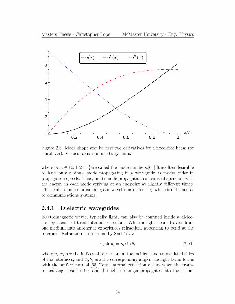
where β1 = 1.87510. This mode shape is illustrated in Figure 2.6, along withthe first and second derivatives. The constants βn are the roots of the equation
cos βn cosh βn = −1 (2.88)
22

Masters Thesis - Christopher Pope McMaster University - Eng. Physics
0.2 0.4 0.6 0.8 1x/L
-20
-10
10
20
30
40 u(x) u′ (x) u′′ (x)
Figure 2.5: Mode shape and its first two derivatives for a fixed-fixed beam (orbridge). Vertical axis is in arbitrary units
2.4 Waveguides
A wide variety of structures have been developed to guide the propagation ofelectromagnetic waves. Similar techniques can be used to analyze fiber opticcables for telecommunications, microwave or radio-frequency waveguides forwireless communications and coaxial cables used for television and numerousother applications.
Waveguides are understood by analyzing the effects of the boundary con-ditions they impose on the electric and magnetic fields.14 These boundaryconditions allow for the propagation of waves in a number of modes, whichdescribe the electromagnetic field intensity in the waveguide. Maxwell’s equa-tions are scale-invariant and thus the analyses presented below are independentof frequency. Practical considerations such as absorption and manufacturingtypically dictate the choice of materials.
Many waveguides allow modes to propagate above a cutoff frequency de-termined by the shape and dimensions of the structure. For a metal-walledwaveguide having a rectangular cross-section with dimensions (a, b) the cutofffrequency for TE modes is given by
fc(m,n) =1
2c
√(ma
)2
+(nb
)2
(2.89)
14A brief overview of waveguide theory is provided here. Detailed analyses can be foundin Ida[63] for metallic waveguides or Reed and Knights[64] for dielectric waveguides.
23
Masters Thesis - Christopher Pope McMaster University - Eng. Physics
0.2 0.4 0.6 0.8 1x/L
2
4
6
8
u(x) u′ (x) u′′ (x)
Figure 2.6: Mode shape and its first two derivatives for a fixed-free beam (orcantilever). Vertical axis is in arbitrary units.
where m,n ∈ 0, 1, 2 . . . are called the mode numbers.[63] It is often desirableto have only a single mode propagating in a waveguide as modes differ inpropagation speeds. Thus, multi-mode propagation can cause dispersion, withthe energy in each mode arriving at an endpoint at slightly different times.This leads to pulses broadening and waveforms distorting, which is detrimentalto communications systems.
2.4.1 Dielectric waveguides
Electromagnetic waves, typically light, can also be confined inside a dielec-tric by means of total internal reflection. When a light beam travels fromone medium into another it experiences refraction, appearing to bend at theinterface. Refraction is described by Snell’s law
ni sin θi = nt sin θt (2.90)
where ni, nt are the indices of refraction on the incident and transmitted sidesof the interfaces, and θi, θt are the corresponding angles the light beam formswith the surface normal.[65] Total internal reflection occurs when the trans-mitted angle reaches 90 and the light no longer propagates into the second
24
Masters Thesis - Christopher Pope McMaster University - Eng. Physics
medium. This occurs at an angle of incidence
θi = θc = sin−1 ntni
(2.91)
called the critical angle. Clearly light is reflected from a larger range of anglesas the refractive index difference increases, with ni > nt.
If the incident medium is a slab with two parallel surfaces then the lightbeam can be confined over long distances. If a light beam is totally reflectedthen it was incident and is reflected at an angle θ > θc. However, it will alsobe incident at the same angle θ on the other parallel surface and be reflectedin the same way. Two-dimensional confinement can be arranged by addinganother pair of parallel surfaces perpendicular to the first. A similar line ofreasoning can be used in circular geometries such as optical fibers.
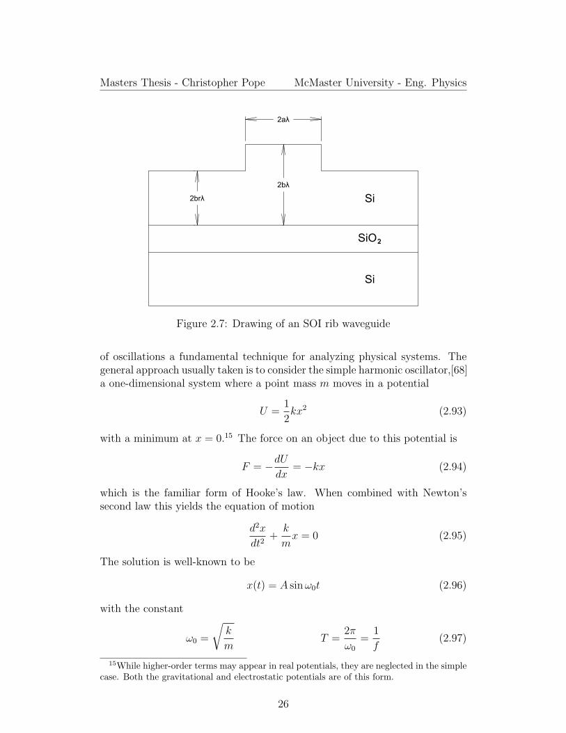
2.4.2 SOI waveguides
Recent advances in silicon-based manufacturing techniques, combined withits low cost compared to III-V semiconductors and the potential to integrateelectronic circuitry has created an interest in silicon-based optical structures,including waveguides.[64] Silicon is transparent in the infrared, for wavelengthslonger than 1.1 µm and has a high dielectric constant, roughly 3.5 around thecommonly used telecom wavelength of 1.5 µm.
A popular method for manufacturing waveguides out of silicon is the silicon-on-insulator (SOI) rib waveguide, illustrated in Figure 2.7. Single-mode wave-guides in this geometry can be designed with heights of several microns, signif-icantly larger than the roughly 200 nm maximum for a rectangular waveguide.The theory behind this geometry was first demonstrated by Soref et al. [66].
For a rib waveguide with a rib height of 2λb, a rib width of 2λa and a slabheight of 2λrb the single-mode condition is
a
b≤ C +
r√1− r2
(2.92)
where C is a fitting constant. The original value was 0.3 from Soref et al., buta stronger condition of C = 0 was imposed by Pogossian et al [67], who alsosuggests using C = −0.05 for design purposes. This is an approximation validfor the case of large rib height (b > 1) and large slab heights (r > 0.5).
2.5 Electromechanical systems
2.5.1 Harmonic motion
Physical phenomena as diverse as guitar strings and orbiting planets may beunderstood in terms of a periodic motion. This commonality makes the study
25
Masters Thesis - Christopher Pope McMaster University - Eng. Physics
2bλ
2brλ
2aλ
Si
SiO₂
Si
Figure 2.7: Drawing of an SOI rib waveguide
of oscillations a fundamental technique for analyzing physical systems. Thegeneral approach usually taken is to consider the simple harmonic oscillator,[68]a one-dimensional system where a point mass m moves in a potential
U =1
2kx2 (2.93)
with a minimum at x = 0.15 The force on an object due to this potential is
F = −dUdx
= −kx (2.94)
which is the familiar form of Hooke’s law. When combined with Newton’ssecond law this yields the equation of motion
d2x
dt2+k
mx = 0 (2.95)
The solution is well-known to be
x(t) = A sinω0t (2.96)
with the constant
ω0 =
√k
mT =
2π
ω0
=1
f(2.97)
15While higher-order terms may appear in real potentials, they are neglected in the simplecase. Both the gravitational and electrostatic potentials are of this form.
26

Masters Thesis - Christopher Pope McMaster University - Eng. Physics
being the angular resonant frequency. The motion is periodic with a periodT .
In general a system undergoing harmonic motion is often subject to somedissipative force, which is typically a function of the system’s velocity. Forsmall velocities this is given by
F = −bdxdt
(2.98)
where b is a constant related to the loss mechanism.16 The resulting equationof motion is
md2x
dt2+ b
dx
dt+ kx = 0 (2.99)
Substituting the resonant frequency from (2.97) and a damping factor
γ =b
2m(2.100)
results in
d2x
dt2+ 2γ
dx
dt+ ω2
0x = 0 (2.101)
The general solutions are of the form
x(t) = Aeat, a = γ ±√γ2 − ω2
0 (2.102)
where the constant a determines the behavior of the system. In the caseγ2 < ω2
0 the constant is complex and the solution can be expressed as
x(t) = Ae−γt sin(ωdt+ φ0) (2.103)
where the damped resonant frequency is
ωd =√ω2
0 − γ2 (2.104)
This solution behaves like free oscillation modulated by an exponential decay.
16This is the first term of a Taylor series expansion of the function F (x). At highervelocities the quadratic term often dominates, but the solution for the linear term is simpler.
27

Masters Thesis - Christopher Pope McMaster University - Eng. Physics
2.5.2 Resonance
It is common to consider the behavior of an oscillating system that is subjectto an external force
F = F0 sinωt or F = F0eiωt (2.105)
which is itself periodic in time. The former form is more typical for describingthe driving force while the latter is more convenient for analysis. The equationof motion is then
md2x
dt2+ b
dx
dt+ kx = F0e
iωt (2.106)
The steady-state solution is a response
x(t) = Aei(ωt−φ) (2.107)
at the driving frequency ω with a phase shift φ relative to the driving force.The amplitude A and phase shift are given by
A =F0/m√
(ω20 − ω2)2 + 4γ2ω2
(2.108)
tanφ =2γω
ω20 − ω2
(2.109)
The phase shift is zero at low frequencies and 180 at high frequencies, pass-ing through 90 at the free resonance frequency ω0. In the undamped case thephase shift is discontinuous at ω = ω0 while the amplitude is infinite. Theresonance behavior in the damped case is plotted in Figure 2.8 for a normal-ized frequency ω/ω0 with a damping coefficient γ = ω0/10. This resonancecondition is useful for improving the signal output from MEMS devices.
While it may not be obvious from Equation (2.108), the amplitude reso-nance of a damped harmonic oscillator is not at the free resonance frequencyω0 but at a resonance frequency
ω2r = ω2
0 − 2γ2 (2.110)
which is determined by differentiating (2.108) to find the maximum.Damping is a dissipative force which implies that energy is leaving the
oscillator at some rate, balanced in the steady-state case by the energy suppliedby the driving force. This energy balance is responsible for the maximumamplitude at resonance
Amax =F0
2γ√ω2
0 − γ2(2.111)
28

Masters Thesis - Christopher Pope McMaster University - Eng. Physics
0.0 0.5 1.0 1.5 2.0Frequency (ω/ω0 )
0
2
4
6
8
10
Am
plit
ude (F
0/k
)
0.0
0.5
1.0
1.5
2.0
2.5
3.0
3.5
Phase
(ra
d)
Figure 2.8: Plot of amplitude and phase as a function of a normalized frequencyω/ω0 for a driven harmonic oscillator with a damping coefficient γ = ω0/10(Q = 5).
and the shape of the resonance peak. The sharpness of the peak is character-ized by the quality factor Q of the resonator, given by
Q = 2πE
∆E=ωd2γ
(2.112)
which may be approximated by the fractional with of the peak
Q ≈ ω
∆ω=
f0
∆f(2.113)
where the peak width ∆f is taken at the half-energy points.
2.5.3 Capacitive detection
Capacitive detection is commonly used to measure small deflections in MEMSdevices.[27] Capacitors can be fabricated simply by a variety of methods andthe resulting detectors can be quite sensitive. The capacitance between two
29

Masters Thesis - Christopher Pope McMaster University - Eng. Physics
parallel plates with area A separated by a gap d is
C = ε0εrA
d(2.114)
which is a reasonable approximation to many MEMS devices.Measuring capacitance is performed by measuring the current through a
capacitor due to an applied voltage. A capacitor caries a charge Q = CV andthus the current is
i =dQ
dt=
d
dt(CV ) (2.115)
for an applied voltage V . Expanding the derivative gives the current
i = CdV
dt+ V
dC
dt(2.116)
This also illustrates the source of the two methods of measuring capac-itance changes. The first term is the displacement current, used where thecapacitance changes slowly relative to the applied voltage. This is the case formost capacitance meters used for measuring fixed capacitances. The secondterm is the motional current due to the change in capacitance. In MEMSdevices this effect can be used to generate an AC voltage in response to me-chanical motion. This effect is a natural fit with resonators, requiring only aDC bias voltage.
2.5.4 Capacitive actuation
Any charged object, such as the plates of a capacitor will experience an elec-trostatic force. The energy stored in a charged capacitor is
U =Q
2C=
1
2CV 2 (2.117)
where Q is the charge on each plate and V is the electric potential across theplates [48]. Since force is equal to the potential gradient, the force on thecapacitor plates is thus
F =1
2V 2dC
dx(2.118)
in the direction of increasing capacitance. For a parallel plate capacitor thechange in capacitance with distance is
dC
dx= ε0εr
A
(d− x)2(2.119)
If the drive voltage is composed of an AC component and a DC component
V = VDC + v0 cosωt (2.120)
30

Masters Thesis - Christopher Pope McMaster University - Eng. Physics
then the force on the capacitor plate will be given by
F =1
2
[V 2DC +
1
2v2
0 + 2VDCv0 cosωt+1
2cos 2ωt
]dC
dx(2.121)
which gives three distinct force components. The first two terms are DCforces which set the operating point of the resonator. The third term is theresponse at the drive frequency. The fourth term is a response at twice thedrive frequency which comes from an expansion of the cos2 term.17
2.5.5 Effective spring constant
In equilibrium the electrostatic force on a beam is equal to the mechanicalrestoring force
Fmech = Felec (2.122)
kx = εV 2 A
(d− x)2(2.123)
using the electrostatic force for a parallel plate capacitor and the mechanicalforce due to Hooke’s law. Solving this for the displacement x due to an appliedvoltage is difficult, but it is quite easy to find the voltage as a function ofdisplacement
V 2 = x(d− x)2 k
εA(2.124)
It is interesting to consider this equation in terms of the relative displace-ment d/x
V 2 =x
d
(1− x
d
)2 kd3
εA(2.125)
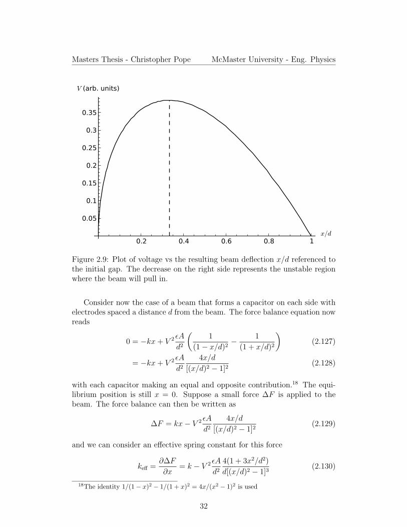
which allows the behavior to be analyzed independent of the initial gap. Thisequation is used to generate the plot in Figure 2.9 which shows the voltagerequired to cause a beam displacement. The required voltage peaks at x/d =1/3 and then decreases, indicating an unstable region where the stiffness ofthe beam is no longer able to overcome the electrostatic force. In this regionthe beam will tend to collapse towards the electrode in a process called pull-inor snap-down, with the potential for destructive results. The pull-in voltageis given by
VP =
√8
27
kd3
εA(2.126)
17Using the identity cos2 x = (1 + cos 2x)/2
31
Masters Thesis - Christopher Pope McMaster University - Eng. Physics
0.2 0.4 0.6 0.8 1x/d
0.05
0.1
0.15
0.2
0.25
0.3
0.35
V (arb. units)
Figure 2.9: Plot of voltage vs the resulting beam deflection x/d referenced tothe initial gap. The decrease on the right side represents the unstable regionwhere the beam will pull in.
Consider now the case of a beam that forms a capacitor on each side withelectrodes spaced a distance d from the beam. The force balance equation nowreads
0 = −kx+ V 2 εA
d2
(1
(1− x/d)2− 1
(1 + x/d)2
)(2.127)
= −kx+ V 2 εA
d2
4x/d
[(x/d)2 − 1]2(2.128)
with each capacitor making an equal and opposite contribution.18 The equi-librium position is still x = 0. Suppose a small force ∆F is applied to thebeam. The force balance can then be written as
∆F = kx− V 2 εA
d2
4x/d
[(x/d)2 − 1]2(2.129)
and we can consider an effective spring constant for this force
keff =∂∆F
∂x= k − V 2 εA
d2
4(1 + 3x2/d2)
d[(x/d)2 − 1]3(2.130)
18The identity 1/(1− x)2 − 1/(1 + x)2 = 4x/(x2 − 1)2 is used
32

Masters Thesis - Christopher Pope McMaster University - Eng. Physics
and at x = 0 the spring constant is
keff|x=0 = k − V 2 4εA
d3(2.131)
Thus, by applying a symmetric bias voltage of magnitude
V =
√kd3
εA(2.132)
to both capacitor arms we can reduce the effective stiffness of the beam tozero. This technique promises to be useful for increasing the sensitivity ofMEMS sensors.
2.5.6 Electrical transduction
This thesis proposes the use of both electrostatic actuation and capacitivesensing, using two capacitors with one side of each being formed by the movingstructure. For such a device at resonance the electrostatic driving force is
F = VDCv0 cosωtdC
dx(2.133)
and the current through the sensing capacitor is
i = VdC
dt= VDC
dC
dx
dx
dt(2.134)
assuming that the capacitors are identical and experience the same potentialVDC . The motion of the structure is as described above
x = Aei(ωt+φ) (2.135)
and the velocity is
dx
dt= iAωei(ωt+φ) (2.136)
with the amplitude A given by Equation (2.108). The current is then
i = V 2DC
(dC
dx
)2v0ω
m√
(ω20 − ω2)2 + 4γ2ω2
ei(ωt+φ) (2.137)
33

Chapter 3
Design and Fabrication
3.1 Fabrication Techniques
3.1.1 Micromachining in Silicon
Micromachining of silicon has been well-developed in the last decades in orderto meet the needs of the semiconductor industry.[69, 29] These techniques havebeen leveraged to fabricate micromechanical systems for a variety of sensorapplications.
The various approaches to microfabrication of microdevices are categorizedas either surface micromachining or bulk micromachining. Surface microma-chining involves the deposition and patterning of surface layers such as metals,polysilicon or silicon oxynitrides on the surface of a wafer, which exists primar-ily to provide mechanical support. This process is closest to CMOS processesused for integrated circuits. Bulk micromachining refers to processes whichmodify the bulk of the wafer, typically by etching, or by bonding multiplewafers together.
Many devices are fabricated by a combination of surface and bulk mi-cromachining processes. Recently a hybrid technique has emerged, based onsilicon-on-insulator (SOI) wafers first developed for the electronics industry. ASOI wafer consists of a thin silicon device layer on a thin buried oxide layer ona standard silicon wafer. In CMOS processes a SOI wafer provides electricalisolation between components when the device layer is etched down to theburied oxide. In MEMS processes it provides a single-crystal silicon surfacelayer on a sacrificial oxide layer.
3.1.2 Anisotropic Etching
Micromachining etching processes are broadly categorized according to whetherthey are directional, wet versus dry, and their selectivity between different ma-
34

Masters Thesis - Christopher Pope McMaster University - Eng. Physics
Isotropic Anisotropic
Wet HNO3+HF (Si), HF (oxide) KOH
Dry XeF2 DRIE
Table 3.1: Examples of etches that can be used for micromachining in silicon.A key advantage of wet etches is that they can be performed in standard labo-ratory glassware and require no special equipment. Deep Reactive Ion Etching(DRIE) can be used to produce highly anisotropic structures, however it re-quires processing equipment. Alkali solutions, such as potassium hydroxide(KOH) stop on 〈111〉 planes in silicon which allows the creation of etch pitswith smooth side-walls, but is limited in the geometry of such structures com-pared to DRIE. For more details see [70, 69, 29].
terials. Selectivity refers to the ratio of the etch rates in two different materials,for example silicon and oxide. High selectivites are useful for stopping etcheson a chosen layer or choosing a masking material for deep etches. Wet etchesare those that have chemicals in aqueous solutions while dry etches are gaseousor plasma processes. Typically, dry etches require dedicated equipment whilewet etches can be performed with standard laboratory glassware.
Anisotropic or directional etches are those that etch at different rates indifferent directions, while isotropic etches proceed at the same rate in all direc-tions. Anisotropic etches are useful for defining features such as flat or verticalside-walls. Chemical etches which display anisotropic behavior in crystals typ-ically do so along well-defined crystal planes. In single-crystal silicon this effectcan be used to produce structures which are smooth down to nearly the atomiclevel.
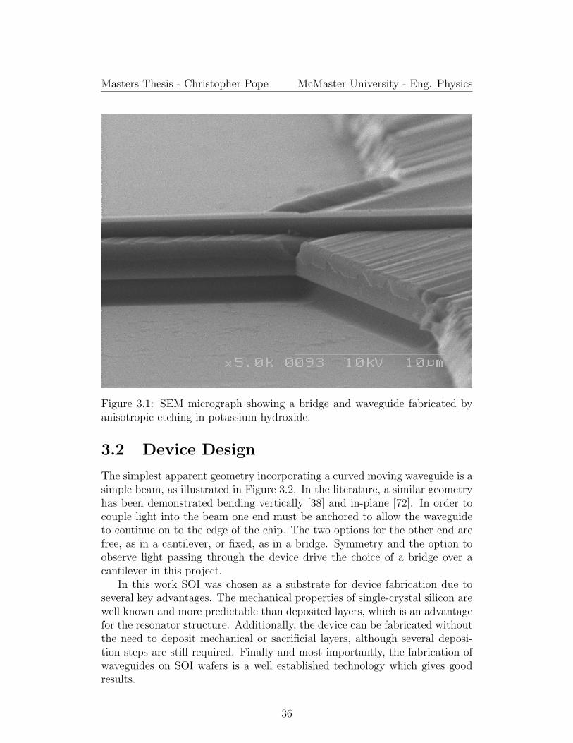
The most common anisotropic wet etches for silicon are alkali or basicsolutions such as potassium hydroxide (KOH) and tetramethyl ammoniumhydroxide (TMAH). These chemicals attack the 〈111〉 crystal planes up totwo orders of magnitude slower than either the 〈100〉 or 〈110〉 planes. In a〈110〉 wafer the 〈111〉 planes form a 54 angle with the surface which producespyramidal pits. In a 〈110〉 wafer there are 〈111〉 planes perpendicular to thesurface, allowing the fabrication of structures with straight and parallel verticalsidewalls. The two vertical 〈111〉 planes form a 109 angle and therefore cannotbe used to create rectangular structures. Figure 3.1 shows the intersection oftwo 〈111〉 planes on a 〈110〉 surface produced by a KOH etch.
35
Masters Thesis - Christopher Pope McMaster University - Eng. Physics
Figure 3.1: SEM micrograph showing a bridge and waveguide fabricated byanisotropic etching in potassium hydroxide.
3.2 Device Design
The simplest apparent geometry incorporating a curved moving waveguide is asimple beam, as illustrated in Figure 3.2. In the literature, a similar geometryhas been demonstrated bending vertically [38] and in-plane [72]. In order tocouple light into the beam one end must be anchored to allow the waveguideto continue on to the edge of the chip. The two options for the other end arefree, as in a cantilever, or fixed, as in a bridge. Symmetry and the option toobserve light passing through the device drive the choice of a bridge over acantilever in this project.
In this work SOI was chosen as a substrate for device fabrication due toseveral key advantages. The mechanical properties of single-crystal silicon arewell known and more predictable than deposited layers, which is an advantagefor the resonator structure. Additionally, the device can be fabricated withoutthe need to deposit mechanical or sacrificial layers, although several deposi-tion steps are still required. Finally and most importantly, the fabrication ofwaveguides on SOI wafers is a well established technology which gives goodresults.
36

Masters Thesis - Christopher Pope McMaster University - Eng. Physics
Figure 3.2: Rendering of the device design. Created in Google Sketchup [71].
Electrostatic techniques were chosen for both driving and detecting themotion of the beam. Capacitive detection is very sensitive while capacitive ac-tuation is essentially the only technique available in this geometry. Electrodesare placed parallel to the bridge, with two electrodes on each side. This allowsfor a variety of electrostatic drive and detection options which are discussedin more detail in Section 4.1.1.
Optical confinement is obtained by fabricating rib waveguides of the typediscussed in Section 2.4.2. Rib waveguides were chosen because of their goodoptical performance [64] and local experience with fabrication and experimen-tal work [73]. To maximize the device sensitivity it was necessary to minimizethe bridge and thus the waveguide width. To this end a waveguide width of4 µm was chosen, equal to the device layer thickness. Using the condition
a
b≤ −0.05 +
r√1− r2
(3.1)
we get a constraint
21
29≤ r ≤ 1 (3.2)
on the height of the slab portion of the waveguide structure, to guaranteesingle-mode operation. The slab height should therefore be greater than 75 %
37

Masters Thesis - Christopher Pope McMaster University - Eng. Physics
of the rib height. This corresponds to an etch depth of 1 µm, however, anetch depth of 800 nm is chosen to provide a safety margin. Polished waveguideend facets were chosen as the means to allow the introduction of light into thewaveguides by fiber butt-coupling.
The remaining device dimensions were determined based on several con-straints. The thickness of the structures is set by the 4 µm device layer ofthe SOI wafers on-hand. Practical limitations in the photolithography processplace a lower limit of 2 µm on feature sizes. The bridge-electrode gap is thuschosen to be 3 µm so as to provide some safety margin while maximizing sen-sitivity. A bridge width of 10 µm was selected to provide the softest possiblemechanical structure while still allowing the alignment and fabrication of aco-located waveguide.
Bridge lengths between 200 µm and 1000 µm were chosen to provide a va-riety of resonant frequencies. The longer bridges provide higher sensitivityby means of a lower spring constant, proportional to 1/L3. An upper limitis placed on bridge length due to concerns about being able to fabricate andrelease such long, soft structures. The exact limit is not known for this geom-etry; a spread of lengths was chosen in the hope that shorter devices wouldsurvive if longer ones did not.
Five devices with bridge lengths stepped by 200 µm were laid out on a chipto simplify processing and handling. This chip layout is illustrated in Figure3.3. The chip is approximately 5 mm by 9 mm, with the longer dimensionchosen to fit in a 10 mm chip holder supplied with the critical point dryer.Eight of these chips, along with test structures and alignment markers werearranged on an approximately 25 mm square die. Mask fields were designed toenable the fabrication of this die as a whole. A drawing of the device is shownin Figure 3.4a.
3.3 Fabrication
The devices are fabricated on a commercially available SOI substrate. Thedevice layer is 4 µm thick and has a 〈110〉 orientation. The buried oxide is2 µm thick and the handle wafer is 500 µm thick with a 〈110〉 orientation. Thedevice layer is high resistivity, > 50 Ω cm to reduce optical absorption.
Broadly, the fabrication procedure consists of patterning the mechanicaland optical structures, making electrical contacts, preparing devices and re-leasing the mechanical structures. The process has five photolithography steps,several wet etches, an ion implantation and a metal deposition. Photolitho-graphic masks are illustrated in Figure 3.4 and cross-sections of the resultingdevice are shown in Figure 3.5.
38

Masters Thesis - Christopher Pope McMaster University - Eng. Physics
Figure 3.3: Section of the mask showing five bridges laid out on a chip. Thepattern is repeated above and below for a total of four rows, and stepped tothe left for a total of two columns and eight chips.
3.3.1 Alignment
The anisotropic etching of silicon in alkali solutions is sensitive to the exactalignment of the etch mask to the crystal planes in the sample. Misalignmentwill cause undercutting of the mask and may cause roughening of the sidewallsor distortion of the structure’s shape. To improve pattern transfer from themask to the sample it is thus beneficial to align to crystal planes in the samplewith high accuracy. A procedure was developed to identify and align to the〈111〉 crystal plane in a 〈110〉 silicon wafer.
This procedure was adapted from an example in literature [74, 75] and usesa single mask, shown in Figure 3.4b. The alignment target is two fan patternson opposite sides of the sample, formed by line segments rotated in 0.1 stepsaround a common point. When these lines are etched into the sample, theetch mask will be undercut where it is misaligned relative to the 〈111〉 plane.The line which is undercut the least is therefore the best aligned to the crystalplane. A matching line on the next mask forms an alignment target whichallows for accurate rotational alignment to the 〈111〉 plane.
The alignment pattern is the first step performed. The pattern is trans-ferred to the sample using the same process described below for the bridgeand waveguide fabrication. Longer etch times, up to twice the thickness of thedevice layer, are used to increase undercutting and allow the alignment to bedetermined more easily.
39

Masters Thesis - Christopher Pope McMaster University - Eng. Physics
(a) Device layout (b) Alignment mask
(c) Bridge mask (d) Waveguide mask
(e) Doping mask (f) Metalization mask
Figure 3.4: Simplified versions of the photolithography masks used in thefabrication process. Etch and doping masks are protected where dark. Metalmask deposits metal where dark.
40

Masters Thesis - Christopher Pope McMaster University - Eng. Physics
Si (4μm)
Si02 (2μm)
Si (500μm)
(a) Initial stack (b) Bridge
(c) Waveguide (d) Electrodes
(e) Released
Figure 3.5: Diagram showing the device cross-sections after various processsteps.
41

Masters Thesis - Christopher Pope McMaster University - Eng. Physics
3.3.2 Bridges and Waveguides
The bridge structures and waveguide ribs are defined with very similar pro-cesses, differing primarily in the pattern and the etch depth. The bridgesand waveguides run parallel to the 〈111〉 crystal planes, allowing the creationof smooth vertical sidewalls by means of an anisotropic potassium hydroxide(KOH) etch. The etchant is prepared as 40% weight KOH using the ratio of80.5 g of KOH to 100 mL of water. The addition of 25 mL of isopropyl alcohol(IPA) reduces the surface tension of the solution to reduce bubble formationand surface roughness, but also changes the etch rate.
An oxide hard mask is used to mask the KOH etch. The oxide is grownby chemical vapour deposition (CVD) to a thickness of approximately 150 nm.Silicon oxide etches significantly slower than silicon in KOH [70] and is thus aconvenient mask. A photoresist layer was spun on on-top of the oxide to allowphotolithographic patterning.1
The photoresist is patterned by contact photolithography using the patternappropriate to the current process step (see Figure 3.4) and developed accord-ing to the manufacturer’s instructions. The pattern is then transferred to theoxide mask by etching in buffered HF (BHF). Following this, the photoresistpattern is stripped using acetone. The silicon etch is performed in 40% weightKOH at 75 C based on a locally developed recipe [73]. The etch depth is con-firmed by a surface profilometer (Tencor AlphaStep 200). Following successfulcompletion of the etch the oxide hard mask is stripped in BHF.
The bridge etch is performed to the full thickness of the device layer, stop-ping on the buried oxide. The alignment marker etch is performed to the samedepth and allowed to run longer to increase the degree of undercutting. Thewaveguide ribs are etched to a depth of 0.8 µm to 1 µm, as discussed in Section3.2.
3.3.3 Contacts
The device layer has a low conductivity to reduce absorption by free carriers,but this is undesirable for the electrical performance of the device. In orderto optimize both the electrical and optical properties of the device, a selectivedoping step was performed. The doping mask exposes the bridge and electrodesidewalls and the contact pads while protecting the waveguide.
A layer of photoresist is spun on, patterned with the doping mask (figure3.4e) and developed according the the manufacturer’s instructions. Doping isperformed by ion implantation of phosphorus at an energy of 15 keV to a dose
1A negative photoresist (Futurrex NR9-1500P) is used for the alignment marker andbridge patterning steps while a positive photoresist (Shipley SC1827) is used for the waveg-uide, doping and metalization steps. The photoresist is chosen based on the mask tone anddoes not represent any fundamental requirement.
42
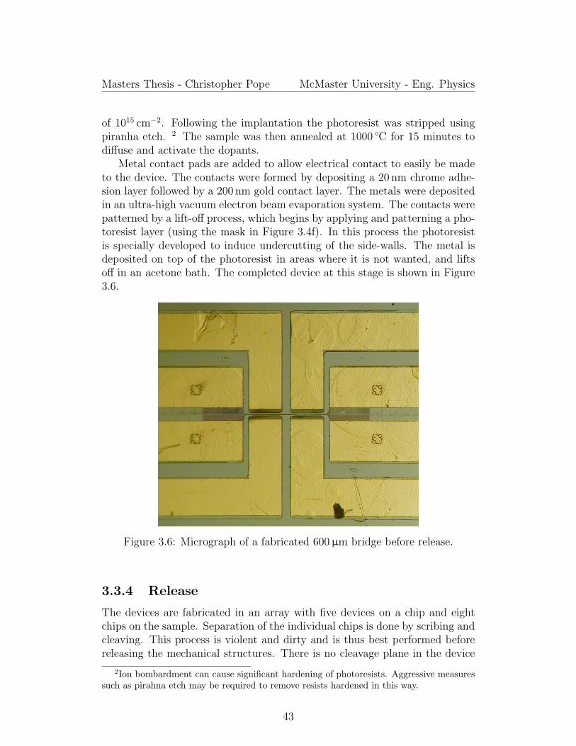
Masters Thesis - Christopher Pope McMaster University - Eng. Physics
of 1015 cm−2. Following the implantation the photoresist was stripped usingpiranha etch. 2 The sample was then annealed at 1000 C for 15 minutes todiffuse and activate the dopants.
Metal contact pads are added to allow electrical contact to easily be madeto the device. The contacts were formed by depositing a 20 nm chrome adhe-sion layer followed by a 200 nm gold contact layer. The metals were depositedin an ultra-high vacuum electron beam evaporation system. The contacts werepatterned by a lift-off process, which begins by applying and patterning a pho-toresist layer (using the mask in Figure 3.4f). In this process the photoresistis specially developed to induce undercutting of the side-walls. The metal isdeposited on top of the photoresist in areas where it is not wanted, and liftsoff in an acetone bath. The completed device at this stage is shown in Figure3.6.
Figure 3.6: Micrograph of a fabricated 600 µm bridge before release.
3.3.4 Release
The devices are fabricated in an array with five devices on a chip and eightchips on the sample. Separation of the individual chips is done by scribing andcleaving. This process is violent and dirty and is thus best performed beforereleasing the mechanical structures. There is no cleavage plane in the device
2Ion bombardment can cause significant hardening of photoresists. Aggressive measuressuch as pirahna etch may be required to remove resists hardened in this way.
43

Masters Thesis - Christopher Pope McMaster University - Eng. Physics
layer perpendicular to the waveguides, so some polishing may be required toget facets of optical quality.
Releasing of the mechanical structures is performed by etching the oxidelayer in 49% HF to undercut the bridges, followed by processing in a criticalpoint dryer (Tousimis Autosamdri-815 Series B). Critical point drying wasused to eliminate surface tension during the drying process which has thepotential to destroy structures in this size range. In this process the sampleis rinsed in DI water following the HF etch and then transferred to a bathof isopropyl alcohol 3 without allowing the sample to dry. Water is displacedby the alcohol, and the sample is transferred to the critical point dryer underliquid. Liquid carbon dioxide (LCO2) is the working fluid in the critical pointdryer. The dryer purges the alcohol from the chamber and carries out thedrying cycle automatically.
By raising the temperature and pressure, the CO2 is taken past its criticalpoint (31 C and 7.4 MPa for CO2). Controlled decompression allows the CO2
to be exhausted as a gas. Because the gas and liquid phases cease to be distinctpast the critical point (where the gas-liquid phase transition curve ends) thesample can be dried without the liquid experiencing a phase transition. Thus,there is no gas-liquid interface to create surface tension which could damagethe structures. The structure released by these techniques is shown in Figure3.7, where the undercut bridge is visible.
In order to perform electrical tests, the chips are mounted to custom-designed printed circuit boards (PCBs). PCBs were found to provide superiorelectrical performance and repeatability when compared to alternatives suchas mounting to DIP headers. The chips were mounted using silver paint. Elec-trical connections were made by wire-bonding to the PCB using gold wire anda ball bonder (Kulicke & Soffa 4522). Details of the electrical connections willbe discussed in Section 4.1.1.
3.4 Fabrication challenges
3.4.1 Facet quality
As discussed above, coupling of light into the waveguides is to be accomplishedby means of butt-coupling of a cleaved fiber to the waveguide end-facet. Max-imizing the coupled power requires that the waveguide facet be smooth andclean to minimize scattering. Typically this is accomplished by cleaving, how-ever this proves to be difficult in this case. Because the waveguides are parallelto the 〈111〉 plane in the 〈110〉 device layer there is no cleavage plane perpen-
3Isopropyl alcohol is used at the manufacturer’s recommendation. IPA is miscible withboth water and LCO2, allowing the water to be completely eliminated.
44

Masters Thesis - Christopher Pope McMaster University - Eng. Physics
Figure 3.7: SEM micrograph of a fabricated and released bridge.
dicular to the waveguide. A further complication is that the thickness of thehandle wafer is, at 500 µm quite thick and difficult to cleave. Finally, while itis the device layer that must cleave cleanly to produce a facet, it is the handlewafer that provides the bulk of the mechanical strength and thus dominatesthe cleavage behavior.
In the first fabrication batch, the device-bearing chips were separated byfirst scribing along scribe marks on the sample and then cleaving along thescribed line. This was successful at separating the chips but did not producea high-quality facet. A SEM image of an edge of a typical chip is presentedin Figure 3.8 showing the roughness left by the scribing and cleaving process.The illustrated waveguide facet is completely unsuitable for optical coupling.
A simple resolution to this issue would be to polish the facet, as the processfor doing so is well understood. Polishing must be done prior to releasing themechanical structure or else there is a risk of damaging the delicate bridges.An alternate solution would be to use a dicing saw to separate the chips. Thequality of the resulting facets is uncertain and it shares at minimum the samedamage risks as polishing. A long-term option is to redesign the device touse grating couplers [76] which allow coupling light into the surface of the
45

Masters Thesis - Christopher Pope McMaster University - Eng. Physics
Figure 3.8: SEM micrograph showing the cleaved edge of a device and theresulting damage to the device layer.
waveguide. While a grating coupler eliminates concerns about facet quality(by eliminating their use entirely) it requires more from the fabrication process.As an optically resonant structure, a grating coupler requires features on theorder of the optical wavelength which would be difficult to obtain in the currentmanufacturing process.
3.4.2 Bridge curvature
Upon releasing devices from the first fabrication run it was discovered thatthe longer bridges were curved up out of the plane, as shown in Figure 3.9.While not significant at shorter lengths, the curvature is enough to raise the1000 µm bridge substantially away from its electrodes. This is a cause forconcern as it decreases the bridge-electrode capacitance due to the decrease inoverlap area. A mitigating factor is that in the proposed experiment designthere exists an electrostatic potential between the bridge and the substratewhich would oppose and possibly correct this curvature.
While the cause of this curvature is unknown, it is believed to be due tothe post-implant anneal process performed in the doping step. The thermal
46

Masters Thesis - Christopher Pope McMaster University - Eng. Physics
Figure 3.9: SEM micrograph showing a released 1000 µm bridge curved up outof the plane of the device layer.
expansion coefficients of silicon and the underlying oxide are different4, whichwould lead to a strain buildup at the annealing temperature of 1000 C. Ifany of this strain was relaxed while at this temperature there would be aresidual strain when the structure is cooled. Such an effect is mentioned in theuser’s guide for the commercial SOIMUMPs process [78], which recommendsa maximum length of 500 µm for 6 µm wide structures anchored at both ends.
Because silicon expands and contracts faster than the oxide, the built-instrain after a relaxation at high temperatures will place the silicon side ofthe interface in tension and the oxide side in compression. When the oxideis etched away during the device release step, the silicon layer will be free tomove and contract at the former interface in order to relieve the built-in strain.This causes the upward deformation of the bridge into its fundamental mode,where the middle half of the bridge is in tension on top and compression onthe bottom.
4Fused quartz has a thermal expansion coefficient of 0.55× 10⁻⁶ K−1 while for silicon itis 2.6× 10⁻⁶ K−1 [77]
47

Masters Thesis - Christopher Pope McMaster University - Eng. Physics
The maximum value for the strain in the silicon layer is
ε = (αSi − αSiO2)∆T (3.3)
which is equal to −2.05× 10⁻³ if the structure is completely relaxed at theannealing temperature.
48

Chapter 4
Experiment
4.1 Electrical Experiment
4.1.1 Electrical connections
Devices were fabricated following the procedure outlined in Section 3.3. Theresulting device is shown in Figure 3.6. There are nine electrical connections:four electrodes, four (theoretically identical) bridge contacts and the substrate.Figure 4.1 shows the six fundamental terminals in relation to the capacitancesof interest. Not shown are parasitic capacitors formed between adjacent elec-trodes and between each electrode and the substrate. These parasitics arepotentially quite significant as they are orders of magnitude larger than theworking capacitances due to the larger areas involved. Proper measurementtechnique can reduce the impact of this issue.
Several methods exist to connect the device to laboratory test and measure-ment equipment. Three methods that were explored are probes, DIP headermounting and PCB mounting. The key evaluation criteria is electrical perfor-mance, requiring low parasitics, low noise and repeatable results. Mechanicalstability and ease of use also played a role in the evaluation.
Probes for making contact to integrated circuits are commonly availablecommercially, and some varieties can offer good performance. Connections toseveral devices were made using a commercially available two-terminal probestation and capacitance measurements were made successfully. While thismethod offers a simple way to test the electrical properties of the device, severalissues were identified which made it unsuitable for further experiments. Theprobe tips in this setup were unshielded and therefore had significant mutualcapacitance, larger than the working capacitance of the device. This can beseen simply by making consecutive measurements of the device and then liftingthe probes slightly from the surface. Additionally, the system is large andexpensive compared to other options and lacks the mechanical integrity that
49

Masters Thesis - Christopher Pope McMaster University - Eng. Physics
CBCA
CCCD
A
D
B
C
G
S
Cbridge
Figure 4.1: Schematic drawing showing the terminals available for makingconnection to the bridge resonator. The capacitors shown are formed betweenthe bridge (terminal G) and the drive/detect electrodes. The capacitor Cbridgeis formed between the bridge and the substrate (terminal S). Not shown arevarious parasitic capacitances.
is desired for long-term measurements.A second option was to use a standard Dual Inline Pin (DIP) package of
the type commonly used for integrated circuits commercially. Previous worklocally has advanced this method for testing MEMS devices [79]. This wasexplored by mounting a device to a 20-pin metal DIP package using conductivesilver paint. Electrical connections were made by wire-bonding from the devicecontact pads to the package pins, using gold wire and an ultrasonic ball bonder.This method, standard practice in the IC industry, was found to require someskill but produces reasonably durable connections.
The DIP package was placed inside a metal box which acted as a Faradaycage. Short wires were soldered between the DIP package pins and BNC con-nectors on the box, allowing the attachment of standard coaxial cables. Mea-surements were made successfully in this setup, however it was not withoutproblems. The hook-up wires used to connect the device to the cables showedsignificant mutual capacitance, at lengths of approximately 5 cm. This capac-itive coupling allowed significant amounts of drive signal to contaminate theoutput signal which complicated measurements.
50

Masters Thesis - Christopher Pope McMaster University - Eng. Physics
To some extent this coupling can be reduced by replacing the hook-up wirewith coaxial cable. Improvements due to the shielding effect of the coaxial ca-ble’s grounded shield were shown experimentally. Soldering connections to thestiffer shielded cable was difficult in the confinement of the Faraday cage. Oneconnection was made successfully, however the difficulty increased with addi-tional connections. While these problems were potentially resolvable througha redesigned enclosure, when combined with ongoing concerns about mechan-ical reliability it was decided to investigate a simpler and cheaper alternative.This investigation began with printed circuit boards, based partly on their usein a recent paper [80].
Products from the cheapest toys to complex microwave circuits bond semi-conductor devices directly to circuit boards for reasons of cost and electri-cal performance. The motivation in this case was the ability to effectivelyshield traces on the PCB by means of a large ground plane, reducing issuesthat affected the alternative methods described above. In addition, standardPCB-mount coaxial connectors could be used to make completely shieldedconnections to measurement equipment.
Custom PCBs were designed based on the above goals. The second revisionof the board is shown in Figure 4.2. The device was mounted to the large pad,with three smaller pads provided on each side for connecting electrodes andthe bridge. All electrical connections are routed to SMA connectors allowingthe attachment of coaxial cables. The board size is only 50 mm square, limitedby mounting holes and the minimum spacing required by the connectors.
Figure 4.2: Design of the PCB on which devices were mounted and tested.Finished board size is two inches square and contained a full ground-plane.The board was designed using EagleCAD [81].
51

Masters Thesis - Christopher Pope McMaster University - Eng. Physics
Inspiration was taken from PCB design rules for high-speed electronic cir-cuits, in particular with respect to reducing capacitance issues, although theoperating frequencies here are low by modern standards [82, 83]. Signal tracesare kept as short as possible and well-seperated to reduce mutual capacitance.The entirety of the board surface area, except where signal traces are routed,forms a single ground plane which is connected to the shields of the SMAconnectors. Six mounting holes are provided on 0.5 inch centers to accept #8-32 screws, which offers compatibility with standard optical components. Theoff-center device mounting position is influenced by the needs of the opticalexperiment described in Section 4.4. A photo of the finished PCB with devicemounted is shown in Figure 4.3.
Figure 4.3: Photograph of a completed PCB with a device mounted and readyfor testing.
4.1.2 Capacitance measurements
Initial capacitance measurements were performed with an Andeen-HagerlingAH 2500A automatic capacitance bridge.1 This instrument allows measure-ment of both the capacitance and loss or parallel conductance of the deviceunder test (DUT). In order to reduce the effects of parasitic capacitances whichmay appear between the terminals of the DUT, or be contributed by cablesand test fixtures, the AH2500 makes three-terminal measurements.
The three-terminal measurement technique, illustrated in Figure 4.4, in-volves ensuring that all spurious or parasitic capacitances are grounded, with
1The manual for this instrument provides an excellent overview of the techniques ofhigh-precision capacitance measurements [84].
52

Masters Thesis - Christopher Pope McMaster University - Eng. Physics
this ground connection forming the third terminal.2 This is typically accom-plished by grounding all nearby conductive objects or placing the DUT in ametal box. An added advantage is that such an enclosure forms a Faradaycage, isolating the system from RF interference.
The three terminals used to make a simple capacitance measurement arethe excitation (high) terminal, the detection (low) terminal and the groundterminal. When an AC test voltage is applied to the H terminal it also appearsacross the parasitic capacitor CHG, which has no effect on the current throughthe DUT (provided the total current does not exceed the current complianceof the source). The input of the amplifier at the L terminal is a virtual groundand thus collects essentially all the current flowing through the DUT, whichbypasses the higher impedance of CLG. In this way the measurement of thecapacitance CHL is unaffected by the presence of other parasitic capacitances.
CHL
CHG CLG
G
ALH
Figure 4.4: Schematic drawing of a three-terminal measurement circuit.
Two measured capacitance values are of interest in characterizing the de-vice. The first is the capacitance measured between the bridge and the elec-trode, which is the working capacitance responsible for the device motion andthe electrical response. The second is the capacitance between two electrodes,which is representative of the parasitic coupling between the drive and detectelectrodes. The device design attempts to reduce this parasitic by spacing
2Capacitance measurements may be made with between two and five terminals, depend-ing on requirements. Two-terminal measurements simply use the current flowing betweenthe instrument terminals to determine the capacitance. Three-terminal measurements, asdescribed here, improve accuracy and noise immunity. Four-terminal measurements followthe example of four-terminal resistance measurements where separate conductor pairs areused to apply the excitation and make the measurement. This allows for improved accuracywhere losses in the connecting cables may be significant but is typically not applicable tothese small capacitances and distances. A five-terminal measurement combines the featuresof three and four-terminal measurements.
53

Masters Thesis - Christopher Pope McMaster University - Eng. Physics
Length Bridge-Electrode Bridge-Substrate Electrode-Substrate(µm) Capacitance (fF) (pF)
200 0.53 8.9 6.3400 1.4 1.8 6.7600 2.3 2.7 7.2800 3.2 3.5 7.61000 4.1 4.4 8.0
Table 4.1: Calculated device capacitances based on the parallel plate approx-imation. This approximation neglects the effects of fringing fields.
electrodes farther apart (40 µm) than the working capacitor gap of 3 µm. Ex-perimental design attempts to reduce the parasitic coupling by grounding un-used electrodes and the substrate, and by making (effectively) three-terminalmeasurements with the bridge as a virtual ground.
Table 4.1 lists theoretical values for the bridge to electrode working capac-itance, the bridge to substrate capacitance and the capacitance between theelectrode pad and the substrate for all five fabricated bridge lengths. It is ofinterest that the parasitic capacitance between the electrode and the substrateis three orders of magnitude larger than the working capacitances. These val-ues are calculated using the parallel plate approximation (equation (2.114))and do not take into account the contributions from fringing fields at the edgesof the capacitor plate.
Measured values for the two device capacitances of interest are summarizedin Table 4.2. The reported values are measured between two terminals of thedevice mounting system and referenced to a local ground plane appropriatefor the mounting system. Offsets from the capacitance bridge and connectingcables are negligible. Reported values are significantly higher than the esti-mates reported in Table 4.1 due to contributions from fringing fields and themounting system. In particular, adjacent bond wires may contribute on theorder of 10fF, and the printed circuit board contributes approximately 12 fFbetween adjacent pads (but only 0.5 fF between non-adjacent pads).
4.1.3 Experimental setup
A basic measurement circuit for the bridge resonator is illustrated in Figure4.5. This circuit is the combination of an actuation circuit using capacitor Caand a sensing circuit using capacitor Cs. These two components operate andcan be analyzed independently.
54

Masters Thesis - Christopher Pope McMaster University - Eng. Physics
Setup Length Bridge-Electrode Electrode-Electrode(µm) Capacitance (fF)
DIP Header (floating) 600 12 000± 1000 10 000± 1000DIP Header (grounded) 600 250± 75 100± 50DIP Header (shielded) 600 30± 10 20± 10DIP Header (shielded) 400 60± 10 10± 5PCB Mount 600 150± 50 —PCB Mount 1000 150± 50 20± 5
Table 4.2: Summary of measured capacitance values for several device mount-ing options. All measurements were taken using the AH2500A capacitancebridge. Error estimates represent fluctuations in measured values and pad-to-pad variations rather than instrument limitations. Devices mounted to DIPheaders were measured with the substrate floating and grounded, and with acoaxial cable used in place of one hook-up wire.
Actuation of the device is done using an actuation voltage VAC = v sinωtcombined with the bias voltage VDC applied across the capacitor Ca. Based onthe result from Equation (2.121) there will be forces on the bridge which areperiodic and frequencies ω and 2ω. As the bridge is a resonant structure it willrespond most strongly when the force is applied at the mechanical resonancefrequency fr. This results in a motion of the bridge which can be measured.
As the bridge moves. the capacitance Cs changes, and by Equation (2.116)there is a current
i = VdC
dt= VDC
dCsdx
dx
dt(4.1)
through the capacitor which is proportional to the velocity of the bridge. Atresonance the motion of the bridge is periodic with frequency fr and likewisethe current is periodic. This current flows into the charge-sensitive amplifier,or rather though the feedback capacitor Cf . The output voltage is
Vout = −iZf =−VDCωCf
dCsdx
dx
dt(4.2)
which is independent of the drive frequency ω if the motion of the bridge issinusoidal. This may be contrasted with a transimpedance amplifier (Zf = Rf )where the output voltage is proportional to the actuation frequency.
An overview of the experimental setup is in Figure 4.6 which shows theequipment used for determining resonant frequencies. All signal connections
55

Masters Thesis - Christopher Pope McMaster University - Eng. Physics
+
Cf
Rf
VDC
CsCa
VACVOut
Figure 4.5: Schematic drawing of the basic drive/detect circuit.
are made using coaxial cables with the shields grounded. Avoiding couplingbetween the drive and detect electronics was a major goal, accomplished largelythough careful grounding of stray capacitance. To this end, all unused deviceterminals were grounded, including the substrate and the ground plane of thePCB, in an attempt to take advantage of the three-terminal measurementtechnique discussed above.
Actuation is accomplished by means of a sinusoidal drive signal providedby a Hewlett Packard (HP) 33120A function generator.3 Bias voltages wereprovided by an HP 3245A universal source or a HP 6212B linear power supply.The HP 3245A has an output range of ±10 V, however this range can be offsetfrom 0 V by stacking its output in series with the HP 6212B as the latter hasfloating outputs and a 100 V output range.
Sensing the device response is done through an Amptek A250 charge sen-sitive preamplifier[85]. This amplifier is chosen for its low noise performanceand performs current to voltage conversion. Output from the amplifier feeds aStanford Research Systems SR844 lock-in amplifier which measures the device
3The Hewlett Packard (HP) equipment used in these experiments was manufacturedprior to the spin-off of HP’s instrument division as Agilent Technologies in 1999. Manualsare available from Agilent via http://agilent.com.
56

Masters Thesis - Christopher Pope McMaster University - Eng. Physics
VAC
A250 VOut
Cb
DUT
SR844Input
Ref
Computer
HP33120
Gnd
Sync1:1
VDC
HP3245
GPIB
Figure 4.6: Block diagram showing the final experiment setup for electricalmeasurements.
response at the drive frequency and performs digital to analog conversion[86].The reference input of the SR844 is fed a square wave from the sync out-put of the HP 33120A, allowing strong rejection of interfering signals at otherfrequencies [87].
The remaining spurious response of the system is due to unavoidable capac-itive coupling between actuation and sensing electrodes (and their associatedbond wires) on the device itself. This leads to an output signal that is thesum of the device response and a static background signal. An attempt toeliminate this was made by balancing out the effects of this parasitic capaci-tance using a variable capacitor and a phase-shifted copy of the drive signalgenerated by a center-tapped transformer. The balancing signal is ideally ofequal magnitude but 180 out of phase which results in a cancelation at theinput of the amplifier.
In the ideal case, where perfect cancelation is achieved, the entire responseof the combined circuit is due to the resonator response. In practice this wasnot perfectly achieved due to experimental difficulties in precisely adjustingthe balancing capacitor. The required value was on the order of 100 fF andgetting even 1 % matching requires extremely small capacitance changes. Theeffect of this imperfect balance is discussed in detail below.
The experiment is controlled by custom software written in National In-struments’ LabVIEW programming language[88]. The computer is connectedto the instruments via an Agilent 82357A GPIB to USB adaptor. The controlsoftware is capable of running automatic frequency sweeps, including multiplesweeps with varying drive and bias voltages.
In order to reduce the damping effects of air on the mechanical structure theelectrical experiments were carried out under vacuum. Reducing the damping
57
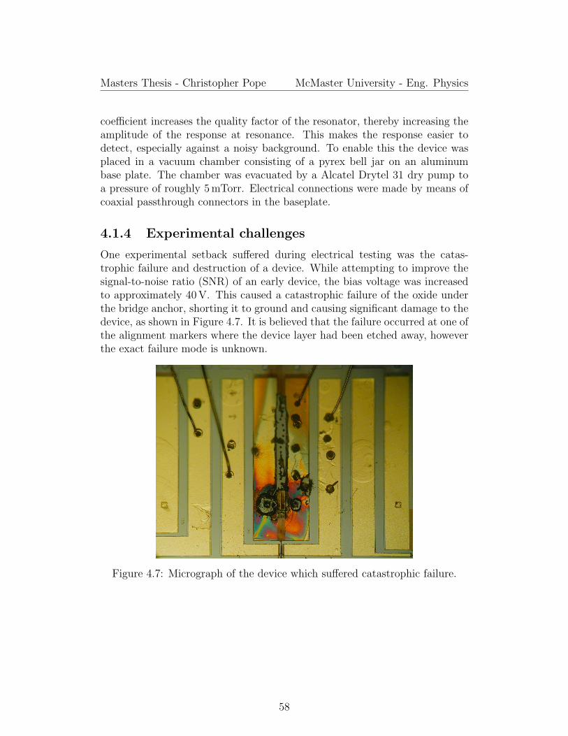
Masters Thesis - Christopher Pope McMaster University - Eng. Physics
coefficient increases the quality factor of the resonator, thereby increasing theamplitude of the response at resonance. This makes the response easier todetect, especially against a noisy background. To enable this the device wasplaced in a vacuum chamber consisting of a pyrex bell jar on an aluminumbase plate. The chamber was evacuated by a Alcatel Drytel 31 dry pump toa pressure of roughly 5 mTorr. Electrical connections were made by means ofcoaxial passthrough connectors in the baseplate.
4.1.4 Experimental challenges
One experimental setback suffered during electrical testing was the catas-trophic failure and destruction of a device. While attempting to improve thesignal-to-noise ratio (SNR) of an early device, the bias voltage was increasedto approximately 40 V. This caused a catastrophic failure of the oxide underthe bridge anchor, shorting it to ground and causing significant damage to thedevice, as shown in Figure 4.7. It is believed that the failure occurred at one ofthe alignment markers where the device layer had been etched away, howeverthe exact failure mode is unknown.
Figure 4.7: Micrograph of the device which suffered catastrophic failure.
58

Masters Thesis - Christopher Pope McMaster University - Eng. Physics
4.2 Resonance Measurements
4.2.1 Results
The experimental setup shown in Figure 4.6 and described above allows theresponse of the resonator to the drive signal to be measured as a functionof several parameters. The most important parameter is the drive frequency,while the response to changing drive and bias voltages are also of interest.Plotting the response of the resonator as a function of frequency gives a re-sult similar to that shown in Figure 2.8, where the peak amplitude occursat the resonance frequency fr. Figure 4.8 shows the measured response of aresonator with a bridge length of 1000 µm in its fundamental in-plane mode,demonstrating a quality factor of 5800. Figure 4.9 shows the response of a600 µm bridge-resonator with a quality factor of 6300. From plots such asthese the resonant frequency and quality factor of the resonators can be de-termined. Results from such determinations are given in Table 4.3, along withtheoretical resonant frequencies.
The device response curve depends on a number of factors, including the
Figure 4.8: Plot showing the response at resonance of a 1000 µm bridge res-onator in response to a drive voltage of 10 mV and a bias voltage of 5 V. Thequality factor of this resonance is approximately 5800.
59

Masters Thesis - Christopher Pope McMaster University - Eng. Physics
Figure 4.9: Plot showing the response at resonance of a 600 µm bridge res-onator in response to a drive voltage of 500 mV and a bias voltage of 5 V. Thequality factor of this resonance is approximately 6300.
actuation conditions, the balancing circuit and some apparently random drifts.The stability of a resonance curve with time is illustrated in Figure 4.10 show-ing the change in curve shape over the course of nearly a day. It may be notedthat the curve in Figure 4.8 and the response in general does not perfectlymatch the theoretical response shown in Figure 2.8. Some of the causes of thisare discussed in Section 4.2.2.
A significant divergence exists between the analytically predicted resonantfrequencies of the devices and the measured results. This is most likely due toa combination of variations in the manufacturing process and inaccuracies inthe approximations used to make the predictions. A narrower than expectedbridge would result in a lower than predicted resonant frequency. This may becaused by undercutting of the mask during the anisotropic etching step. Thebridge length is greater than the design length due to etching of the anchors,producing the taper shape shown in Figure 3.1. This will also cause a decreasein the resonant frequency.
60

Masters Thesis - Christopher Pope McMaster University - Eng. Physics
Experimental Analytic SimulatedLength (µm) fr (kHz) Q fa (kHz) fs (kHz)
200 — — 2229400 — — 557600 158 6300 248800 — — 1391000 58.5 5800 89.1
Table 4.3: Summary of experimental, analytical and simulated resonant fre-quencies. Experimental frequencies are approximate as they vary with thedrive and bias voltages. Frequency is ±2 %, quality factor is ±10 % based onobservation. Quality factor was determined from Figure 4.8 for the 1000 µmdevice, and from Figure 4.9 for the 600 µm bridge. These Figures are rep-resentative of the device response. Analytic frequencies are calculated usingEquation (2.77) using the Young’s modulus for the 〈211〉 direction from (2.68).
4.2.2 Signal and background
As discussed above, there are parasitic capacitances which inject some frac-tion of the drive signal into the response of the resonator. This backgroundsignal is difficult to prevent or filter out and contributes to some extent tothe measured response of the device in all cases. A balancing technique wasemployed to greatly reduce the contribution of this background signal to themeasured response, which improves the sensitivity of the experiment. Fig-ure 4.11 compares the signal measured with and without the addition of thebalancing arm.
This background signal can potentially distort both the measured ampli-tude and the phase of the device response. The input signal, and thus thedevice response, is measured by the lock-in amplifier in terms the in-phasecomponent X and the out-of phase component Y .4 The signal componentsare measured at a 90 phase shift, with the in-phase component being in phasewith the reference signal. When the resonator response is combined with thebackground signal, these components may be expressed as
X = X(ω) +Xb Y = Y (ω) + Yb (4.3)
which again take the form of a frequency-dependant response against a staticbackground.
4These components are sometimes labeled I and Q (for quadrature)
61

Masters Thesis - Christopher Pope McMaster University - Eng. Physics
Figure 4.10: Plot showing stability of the resonance peak over time. The firstsweep is plotted in green, the last sweep is plotted in blue and the interveningsweeps show a gradient. The data set contains 28 sweeps taken over 21 hours,each sweep lasting 45 minutes. Changes in the shape and position of thecurves may be due to drifts in the device response, the balancing circuit or themeasurement equipment. Actuation is at 500 mV with a 5 V bias.
The quantities of interest for analyzing the resonator response are the mag-nitude
R =√X2 + Y 2 (4.4)
and the phase
φ = arctanY
X(4.5)
which correspond to the analysis in Section 2.5.2. If the background signal islarge relative to the resonator response then the magnitude of the change inthe calculated phase will be significantly smaller than the change in the phaseof the real resonator response. This effect was observed experimentally. Theeffect of the background on the calculated magnitude is more complex, andthis is believed to explain the difference between the shape of the experimentalresonance curves and the theoretical response of a simple harmonic oscillator.
62

Masters Thesis - Christopher Pope McMaster University - Eng. Physics
Figure 4.11: Plot showing the device response improved balancing. The back-ground signal is reduced (shifted down) and the phase change increases.
4.2.3 Overdriving
The phenomenon of pull-in, whereby a sufficient bias voltage across the resonator-electrode gap might cause collapse of the structure was discussed in Section2.5.5. That analysis was performed at DC and does not take into accountthe quality factor of the resonator which increases its motion at resonance,potentially by several orders of magnitude. Measurements of resonators madeat high bias voltages and, in general high values of the average drive voltageVavg =
√VACVDC lead to the observation of a clipping behavior in the device
response. A characteristic plot of this clipped response is shown in Figure4.12.
This clipped response takes the form of a sharp drop in the signal ampli-tude as the drive frequency approaches the resonant frequency of the structure.Many such drops and recoveries are observed as the drive passes through res-onance until the device settles to its lower response above resonance. Closeexamination of this effect revealed that this clipping behavior happened be-tween adjacent data points even as the frequency step between each point wasreduced significantly. The cause of this clipping behavior appears to be anexcessive amplitude of the actuation force resulting from the product of the
63

Masters Thesis - Christopher Pope McMaster University - Eng. Physics
0 20 40 60 80 100 120 140Frequency (Hz) +1.585e5
0.00250
0.00255
0.00260
0.00265
0.00270
Sig
nal (V
rms)
(a) 1 V actuation
0 20 40 60 80 100 120 140Frequency (Hz) +1.585e5
0.00130
0.00132
0.00134
0.00136
0.00138
Sig
nal (V
rms)
(b) 0.5 V actuation
Figure 4.12: Contrast between overdriven and normal response. Measurementswere made consecutively on a 600 µm bridge under 5 V bias.
actuation and bias potentials exceeding some limit. Reducing the actuationamplitude reduced and then eliminated this distortion.
While the physical mechanism behind the clipping response has not beenproven, a reasonable theory may be developed. Recalling from (2.134) thatthe current response of the resonator is proportional to its velocity, the suddendrop in output is likely due to a sharp drop in that velocity. The proposedcause for this sudden drop in velocity is the resonator coming into contact withan electrode due to the greatly increased amplitude of its motion at resonance.5
This drop in velocity would persist for a time period
τ = 2πQ/ωr (4.6)
called the ring-down time, where Q is the quality factor. This period is lessthan one second for the devices measured here which would explain the inter-mittent nature of the effect. It should be noted that while the cause of thiseffect has not been proven experimentally the relationship to the actuationvoltage has been demonstrated. This is sufficient to allow the effect to beavoided, as has been done in subsequent experiments.
4.3 Effective Spring Constant
In Section 2.5.5 it was determined that a symmetric electrostatic force actingon a MEMS device could cause a reduction in the effective stiffness of the de-vice. The electrode geometry described here allows such a force to be applied,
5It may be considered surprising that the resonator survives such repeated collisions andis a testament to the durability of MEMS devices.
64
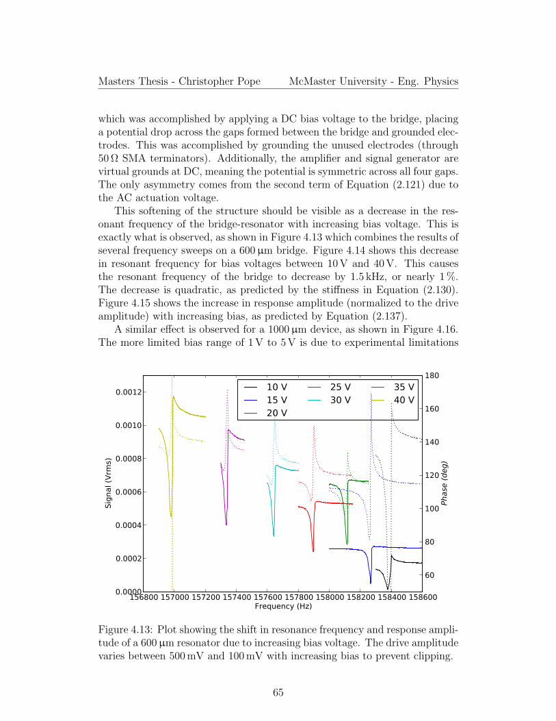
Masters Thesis - Christopher Pope McMaster University - Eng. Physics
which was accomplished by applying a DC bias voltage to the bridge, placinga potential drop across the gaps formed between the bridge and grounded elec-trodes. This was accomplished by grounding the unused electrodes (through50 Ω SMA terminators). Additionally, the amplifier and signal generator arevirtual grounds at DC, meaning the potential is symmetric across all four gaps.The only asymmetry comes from the second term of Equation (2.121) due tothe AC actuation voltage.
This softening of the structure should be visible as a decrease in the res-onant frequency of the bridge-resonator with increasing bias voltage. This isexactly what is observed, as shown in Figure 4.13 which combines the results ofseveral frequency sweeps on a 600 µm bridge. Figure 4.14 shows this decreasein resonant frequency for bias voltages between 10 V and 40 V. This causesthe resonant frequency of the bridge to decrease by 1.5 kHz, or nearly 1 %.The decrease is quadratic, as predicted by the stiffness in Equation (2.130).Figure 4.15 shows the increase in response amplitude (normalized to the driveamplitude) with increasing bias, as predicted by Equation (2.137).
A similar effect is observed for a 1000 µm device, as shown in Figure 4.16.The more limited bias range of 1 V to 5 V is due to experimental limitations
Figure 4.13: Plot showing the shift in resonance frequency and response ampli-tude of a 600 µm resonator due to increasing bias voltage. The drive amplitudevaries between 500 mV and 100 mV with increasing bias to prevent clipping.
65

Masters Thesis - Christopher Pope McMaster University - Eng. Physics
10 15 20 25 30 35 40156800
157000
157200
157400
157600
157800
158000
158200
158400 Measured Fitted
Freq
uenc
y (H
z)
Bias (V)
Figure 4.14: Plot of the shift in resonance frequency vs. bias voltage for a600 µm resonator, using the data from Figure 4.16. The polynomial fit showsan intercept at 158 451 Hz± 11 Hz with a slope of 2.50 Hz/V ± 0.94 Hz/V anda quadratic coefficient of −0.982 Hz/V2 ± 0.019 Hz/V2. (R2 = 1.00)
involving the vertical pull-in voltage of the structure. Figure 4.17 shows thedecreasing frequency as a result of the electrostatic softening effect in the sameway as the 1000 µm bridge. Figure 4.18 shows the corresponding increase inresponse amplitude.
The softness of the out-of-plane mode is a limitation when attempting toincrease the bias voltage to improve the device response. This is also a keycomplication when attempting to reduce the effective spring constant of theresonator. The structure is thinner in this direction by roughly a factor of twowhich gives a factor of four in the stiffness. This in turn means that the pull-involtage in the vertical direction is less than that for the in-plane motion. Thusthe DC bias applied to the bridge is limited by this value, when the substrateis grounded.6
There are essentially two solutions to this problem. The first is to biasthe actuation and sensing electrodes separately, as in Figure 4.19. On thesensing side, the resistor Rb must large compared to the input impedance of
6In practice the bias voltage is limited to be less than the calculated pull-in voltage plussome safety margin as determining the pull-in voltage experimentally risks destroying thedevice.
66

Masters Thesis - Christopher Pope McMaster University - Eng. Physics
10 15 20 25 30 35 40
0.000
0.001
0.002
0.003
0.004
0.005
0.006
Measured Fitted
Nor
mal
ized
Res
pons
e
Bias (V)
Figure 4.15: Plot of the device response (peak height) vs. bias voltage for a600 µm resonator, using the data from Figure 4.13. The device response hasbeen normalized to the drive amplitude. The curve is quadratic coefficient(3.62± 0.12)× 10−6 V/V2. (R2 = 0.978)
the amplifier (which is hopefully small) to prevent any of the signal currentfrom flowing into the bias supply instead. The blocking capacitors Cb arepresent to protect the drive and detect electronics from the DC voltages. Thisapproach has the benefit of allowing independent control over the bias voltages.This is in fact a disadvantage when trying to match the bias voltages to softenthe bridge as precise matching of the bias supplies may be required.
A simple alternative available in this geometry is to simply tie the bridgeand substrate together, placing them at the same potential. This providesall the benefits of biasing the bridge while eliminating the electrostatic forcebetween the bridge and substrate. The noise performance should be similaras the DC supply ideally offers a low AC impedance to ground. Isolating thesubstrate was accomplished by placing an isolated pad on the PCB to acceptthe chip and providing it with an independent electrical connection, as seenin Figure 4.2. A solder jumper was provided to easily ground the substrateif required. Future PCB revisions may tie the bridge and substrate togetherdirectly. This technique will be useful for future optical experiments whichintend to induce small changes in the stiffness of the structure. Reducing the
67

Masters Thesis - Christopher Pope McMaster University - Eng. Physics
Figure 4.16: Plot showing the shift in resonance frequency and response am-plitude of a 1 mm resonator due to increasing bias voltage. Actuation is at200 mV.
stiffness electrostatically will allow small absolute changes in the stiffness tocause larger relative changes.
68

Masters Thesis - Christopher Pope McMaster University - Eng. Physics
1 2 3 4 5
58515
58520
58525
58530
58535 Measured Fitted
Freq
uenc
y (H
z)
Bias (V)
Figure 4.17: Plot of the shift in resonance frequency vs. bias voltage for a 1 mmresonator, using the data from Figure 4.16. The linear fit shows an interceptat 58 539.4 Hz± 1.2 Hz with a slope of −4.68 Hz/V ± 0.39 Hz/V. (R2 = 0.979)
69
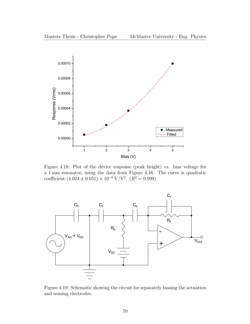
Masters Thesis - Christopher Pope McMaster University - Eng. Physics
1 2 3 4 5
0.00000
0.00002
0.00004
0.00006
0.00008
0.00010
Measured Fitted
Res
pons
e (V
rms)
Bias (V)
Figure 4.18: Plot of the device response (peak height) vs. bias voltage fora 1 mm resonator, using the data from Figure 4.16. The curve is quadraticcoefficient (4.024± 0.051)× 10−6 V/V2. (R2 = 0.999)
+
Cf
Rf
VDC
CsCa
VAC + VDCVOut
Rb
Cb
Figure 4.19: Schematic showing the circuit for separately biasing the actuationand sensing electrodes.
70

Masters Thesis - Christopher Pope McMaster University - Eng. Physics
4.4 Optical Experiment
The electrical and mechanical device design described here is planned to allowtwo key optical experiments to be performed. The first is to measure theeffective stiffness of the optical power confined in the waveguide, as describedin Section 2.2.3. This effect may be observed as a shift in the resonancefrequency of the structure due to a change in the total stiffness of the structurewith increasing optical intensity. Such an effect does not appear to have beenpreviously proposed in the literature. The ability to reduce the effective springconstant of the structure, as demonstrated in Section 4.3 allows an opticalstiffness to be observed more readily by increasing the relative magnitude ofthe optical stiffness vs. the mechanical stiffness.
The second experiment would be to actuate the device optically and observethe resulting resonance capacitively, as has been done for electrical actuation.In order to apply an optical force to the structure, the waveguide must bepre-curved, as the force is proportional to the curvature. This curvature canbe applied electrostatically by means of a DC bias between the bridge and anelectrode, which would induce a deflection of the bridge. If the light coupledinto the waveguide is pulsed at a frequency f then the structure will experiencea force opposing the curvature that is pulsed at the same frequency. Such aforce can be used to excite the structure at resonance.
The devices described above were designed and fabricated for the purposeof demonstrating this effect. Introducing light into the waveguides may beaccomplished by means of butt coupling from the face of a cleaved optical fiberto the end-face of the waveguide. This requires careful alignment of the 10 µmfiber core to the 4 µm waveguide cross-section to provide maximum coupling.To allow this coupling, the system shown in Figure 4.20 was constructed using acombination of commercial optical components and custom mounting brackets.
Using this setup, coupling of light into the waveguides was attempted. Thelight source was a 1550 nm semiconductor laser (JDS Fitel custom assembly)coupled via an FC connector to a single-mode fiber.7 Despite best efforts,coupling of light into the waveguides could not be demonstrated. This isbelieved to be due to the low quality of the waveguide facets. Efforts tofabricate devices with improved waveguide and facet quality are underway.
7A standard telecom fiber, Corning SMF-28 was used. For better coupling efficiency atapered fiber was on hand, but not used. Both fibers were purchased from OZ Optics ofOttawa, Ontario.
71

Masters Thesis - Christopher Pope McMaster University - Eng. Physics
Figure 4.20: Photograph of the assembled electrical-optical-mechanical exper-iment. The system is mounted to a baseplate which accepts a bell jar, allowingthe experiment to be carried out under vacuum.
72

Chapter 5
Conclusion
5.1 Summary
This thesis describes the design, fabrication and operation of silicon microme-chanical resonators and a procedure for using these devices to measure radi-ation pressure due to light confined in a waveguide. The resonators detailedhere consist of a fixed-fixed beam fabricated and released from a SOI wafer bywet chemical etching. A process flow for this fabrication was developed, pho-tolithographic masks were designed and the process flow was executed. Thesebridges were actuated and their motion sensed by capacitive methods. Thefrequency response of the resonators was used to locate and excite the fun-damental in-plane mode of the bridge. Electrostatic tuning of the resonancefrequency via the effective stiffness of the structure was described theoreticallyand demonstrated experimentally.
A number of challenges have been identified in the fabrication process, inthe electrical experiment and in the optical experiment. Causes and poten-tial solutions have been discussed, with many solutions being demonstrated.The usefulness of printed circuit boards as low-cost custom test jigs has beendemonstrated, with results which improve on other available options. Ad-ditionally, the techniques necessary for detecting resonant behavior againstbackground signals have been developed and implemented.
The optical experiment developed in this thesis represents a novel tech-nique for the measurement of electromagnetic momentum. The MEMS de-vices needed to perform this experiment have been designed, fabricated andtested. The electrical, mechanical and software support infrastructure hasbeen designed, acquired, and integrated as necessary.
73

Masters Thesis - Christopher Pope McMaster University - Eng. Physics
5.2 Future Work
5.2.1 Optical experiment
This thesis has described an experiment which would allow the measurementof the optical momentum carried by light in a waveguide. This measurementwas to be performed by the effect of radiation pressure acting inside a curvedwaveguide which was also a mechanical resonator. This geometry does notappear to have been previously proposed for measuring radiation pressure. Asuccessful implementation of this experiment with sufficient resolution wouldallow a statement to be made regarding the Abraham-Minkowski controversyregarding the correct magnitude of the optical momentum in a medium.
Making a quantitative measurement of the momentum carried by lightin the waveguide would represent a significant scientific contribution. As theproposed experiment is different from those carried out so far it would provide aunique perspective on the Abraham-Minkowski controversy. An argument canbe advanced for the Abraham form of the photon momentum being the obviousresult. This is due to the optical force acting inside the mechanical structureand its interaction with the motion of that structure. This would fit withthe identification of the Abraham momentum as the mechanical momentumcarried by light. An appropriate formulation of the problem should also allowthe role of the Minkowski momentum to be demonstrated, as the light is indeedpropagating inside the medium. This would be a demonstration of both formssimultaneously and provide experimental evidence for their equivalence, as hasbeen previously discussed.
While the fabrication and characterization of the mechanical system hasbeen completed, unforeseen experimental difficulties have delayed the opticalexperiment. As the infrastructure for this experiment is in place it shouldbe relatively straight-forward to complete this measurement in the future.Existing designs may be used for the device and the PCB mount. The onlyremaining fabrication challenge is the preparation of optical quality waveguidefacets. Coupling light into the waveguides is the only remaining experimentalchallenge, aside from whatever work may be needed to increase the sensitivityof the experiment.
5.2.2 Revised device design
A new revision of the mask design would allow several improvements to bemade which have the potential to make the experiment easier and more sensi-tive. The first is to locate electrical contacts farther away from the waveguidefacet, separating the electrical and optical connections to the device. Addi-tionally, it would be beneficial to design a structure which implements thebalancing circuit on the same chip as the device. This would allow the reduc-
74

Masters Thesis - Christopher Pope McMaster University - Eng. Physics
tion of the background signal by nulling it though a structure matched to theresonator.
The sensitivity of the future optical experiment could be improved by twomain changes. Since the experiment seeks to measure small changes in thestiffness of the mechanical structure, it is desirable to decrease the initialstiffness so that the relative magnitude of the change is maximized. One wayto decrease the stiffness of the bridge is to increase its length, as the stiffness isproportional to 1/L3. This work has demonstrated the feasibility of releasing1 mm bridges. However that does not appear to be a maximum and longerstructures may be possible. A second option is to fabricate cantilevers insteadof bridges, as the stiffness is lower.
A third technique for decreasing the stiffness of the fabricated devices wouldbe to decrease the bridge width, as the stiffness is proportional to w3 forthe in-plane mode. The current fabrication techniques are near their limitwith respect to alignment of the waveguide on the bridge, however these arenot fundamental physical limitations. Taking advantage of improved opticallithography processes or electron beam lithography would allow the width andtherefore the stiffness of the structures to be reduced. The lower limit on thebridge stiffness would then be due to the need to release the structure.
5.2.3 Electrostatic softening
The results described in Section 4.3 may be considered preliminary work inthis area. The symmetry of the bridge design allows, in theory, for the effectivestiffness of the structure to be decreased to zero. An expanded demonstrationof this effect would be useful for the tuning of MEMS resonators, which wouldhave applications for both frequency references and RF filters. Carrying outthis experiment should be straightforward, taking advantage of the techniquesdemonstrated in this thesis.
75

References
[1] J. Maxwell, A treatise on electricity and magnetism., 1st ed. Oxford,1873. [Online]. Available: http://posner.library.cmu.edu/Posner/books/book.cgi?call=537 M46T 1873 VOL. 2
[2] J. Maxwell, A treatise on electricity and magnetism., unabridged andunaltered republ. of 3. ed. 1891. ed. New York: Dover Publ., 1954.
[3] E. F. Nichols and G. F. Hull, “A preliminary communicationon the pressure of heat and light radiation,” Physical Review(Series I), vol. 13, no. 5, p. 307, Nov. 1901. [Online]. Available:http://link.aps.org/doi/10.1103/PhysRevSeriesI.13.307
[4] E. F. Nichols and G. F. Hull, “The pressure due to radiation,”Proceedings of the American Academy of Arts and Sciences, vol. 38,no. 20, pp. 559–599, Apr. 1903. [Online]. Available: http://www.jstor.org/stable/20021808
[5] P. Lebedew, “Untersuchungen uber die druckkrafte des lichtes,” Annalender Physik, vol. 311, no. 11, pp. 433–458, Jan. 1901. [Online]. Available:http://onlinelibrary.wiley.com/doi/10.1002/andp.19013111102/abstract
[6] A. Ashkin, “Acceleration and trapping of particles by radiation pressure,”Physical Review Letters, vol. 24, no. 4, p. 156, Jan. 1970. [Online].Available: http://link.aps.org/doi/10.1103/PhysRevLett.24.156
[7] A. Ashkin, “Optical levitation by radiation pressure,” AppliedPhysics Letters, vol. 19, p. 283, 1971. [Online]. Available: http://link.aip.org/link/?APL/19/283/1
[8] A. Ashkin, J. M. Dziedzic, J. E. Bjorkholm, and S. Chu, “Observation ofa single-beam gradient force optical trap for dielectric particles,” OpticsLetters, vol. 11, no. 5, pp. 288–290, May 1986. [Online]. Available:http://ol.osa.org/abstract.cfm?URI=ol-11-5-288
[9] A. Ashkin and J. Dziedzic, “Optical trapping and manipulation ofviruses and bacteria,” Science, vol. 235, no. 4795, pp. 1517 –1520,
76

Masters Thesis - Christopher Pope McMaster University - Eng. Physics
Mar. 1987. [Online]. Available: http://www.sciencemag.org/content/235/4795/1517.abstract
[10] S. Chu, L. Hollberg, J. E. Bjorkholm, A. Cable, and A. Ashkin,“Three-dimensional viscous confinement and cooling of atoms byresonance radiation pressure,” Physical Review Letters, vol. 55, no. 1,p. 48, Jul. 1985. [Online]. Available: http://link.aps.org/doi/10.1103/PhysRevLett.55.48
[11] S. Chu, J. E. Bjorkholm, A. Ashkin, and A. Cable, “Experimentalobservation of optically trapped atoms,” Physical Review Letters,vol. 57, no. 3, p. 314, Jul. 1986. [Online]. Available: http://link.aps.org/doi/10.1103/PhysRevLett.57.314
[12] A. Ashkin, “Optical trapping and manipulation of neutral particlesusinglasers,” Proceedings of the National Academy of Sciences of theUnited States of America, vol. 94, no. 10, pp. 4853–4860, May 1997.[Online]. Available: http://www.pnas.org/content/94/10/4853.abstract
[13] W. A. Hollerman, “The physics of solar sails,” Apr. 2003. [Online].Available: http://ntrs.nasa.gov/search.jsp?print=yes&R=20030093608
[14] “IKAROS ProjectJAXA space exploration center,”http://www.jspec.jaxa.jp/e/activity/ikaros.html. [Online]. Available:http://www.jspec.jaxa.jp/e/activity/ikaros.html
[15] “NASA - NanoSail-D home page,”http://www.nasa.gov/mission pages/smallsats/nanosaild.html,NanoSail-D index page. [Online]. Available: http://www.nasa.gov/mission pages/smallsats/nanosaild.html
[16] A. Clarke, “The wind from the sun,” in The collected stories of Arthur C.Clarke., 1st ed. New York: Tom Doherty Associates, 2001, pp. 828–842.
[17] H. Minkowski, “Die grundgleichungen fur die elektromagnetischenvorgange in bewegten korpern,” Nachrichten von der Gesellschaftder Wissenschaften zu Gottingen, Mathematisch-Physikalische Klasse,vol. 53, pp. 53–111, 1908.
[18] H. Minkowski, “Die grundgleichungen fur die elektromagnetischenvorgange in bewegten korpern,” Mathematische Annalen, vol. 68, pp.472–525, Dec. 1910. [Online]. Available: http://www.springerlink.com/content/x709h877x251881u/
77

Masters Thesis - Christopher Pope McMaster University - Eng. Physics
[19] M. Abraham, “Zur elektrodynamik bewegter korper,” Rendiconti delCircolo Matematico di Palermo, vol. 28, pp. 1–28, Dec. 1909. [Online].Available: http://www.springerlink.com/content/j8372431277v5702/
[20] M. Abraham, “Sullelettrodinamica di minkowski,” Rendiconti del CircoloMatematico di Palermo, vol. 30, pp. 33–46, Dec. 1910. [Online].Available: http://www.springerlink.com/content/h30845351ng5tv43/
[21] S. M. Barnett and R. Loudon, “The enigma of optical momentumin a medium,” Philosophical Transactions of the Royal SocietyA: Mathematical, Physical and Engineering Sciences, vol. 368,no. 1914, pp. 927 –939, Mar. 2010. [Online]. Available: http://rsta.royalsocietypublishing.org/content/368/1914/927.abstract
[22] S. M. Barnett, “Resolution of the Abraham-Minkowski dilemma,”Physical Review Letters, vol. 104, no. 7, p. 070401, Feb. 2010. [Online].Available: http://link.aps.org/doi/10.1103/PhysRevLett.104.070401
[23] M. Mansuripur, “Resolution of the Abraham-Minkowski controversy,”Optics Communications, vol. 283, no. 10, pp. 1997–2005, May 2010.[Online]. Available: http://www.sciencedirect.com/science/article/pii/S0030401810000131
[24] W. She, J. Yu, and R. Feng, “Observation of a push force on the endface of a nanometer silica filament exerted by outgoing light,” PhysicalReview Letters, vol. 101, no. 24, p. 243601, Dec. 2008. [Online]. Available:http://link.aps.org/doi/10.1103/PhysRevLett.101.243601
[25] M. Mansuripur, “Comment on ”Observation of a push force on the endface of a nanometer silica filament exerted by outgoing light”,” PhysicalReview Letters, vol. 103, no. 1, p. 019301, Jul. 2009. [Online]. Available:http://link.aps.org/doi/10.1103/PhysRevLett.103.019301
[26] I. Brevik, “Comment on “Observation of a push force on the end faceof a nanometer silica filament exerted by outgoing light”,” PhysicalReview Letters, vol. 103, p. 219301, Nov. 2009. [Online]. Available:http://link.aps.org/doi/10.1103/PhysRevLett.103.219301
[27] V. Kaajakari, Practical MEMS. Las Vegas Nev.: Small Gear Pub., 2009.
[28] R. P. Feynman, “There’s plenty of room at the bottom,” Engineeringand Science, vol. 23:5, Feb. 1960. [Online]. Available: http://resolver.caltech.edu/CaltechES:23.5.0
78

Masters Thesis - Christopher Pope McMaster University - Eng. Physics
[29] M. Madou, Fundamentals of microfabrication : the science ofminiaturization, 2nd ed. Boca Raton: CRC Press, 2002. [Online].Available: http://libcat.mcmaster.ca/index.jsp?Ntt1=1522329&Ntk1=Bib+No.&Ntx1=mode+matchallpartial
[30] A. M. Nicolson, “Generating and transmitting electric currents,” 1918.[Online]. Available: http://www.google.com/patents?vid=2212845
[31] H. C. Nathanson and R. A. Wickstrom, “A RESONANT-GATESILICON SURFACE TRANSISTOR WITH HIGH-Q BAND-PASSPROPERTIES,” Applied Physics Letters, vol. 7, p. 84, 1965. [Online].Available: http://link.aip.org/link/APPLAB/v7/i4/p84/s1
[32] H. C. Nathanson, W. E. Newell, R. A. Wickstrom, and J. R. Davis, “Theresonant gate transistor,” IEEE Transactions on Electron Devices, vol. 14,no. 3, pp. 117– 133, Mar. 1967.
[33] F. Chen, J. Brotz, U. Arslan, C. Lo, T. Mukherjee, and G. K. Fedder,“CMOS-MEMS resonant RF mixer-filters,” in 18th IEEE InternationalConference on Micro Electro Mechanical Systems, 2005. MEMS 2005.IEEE, Feb. 2005, pp. 24– 27.
[34] K. E. Petersen, “Silicon as a mechanical material,” Proceedings of theIEEE, vol. 70, no. 5, pp. 420– 457, May 1982. [Online]. Available:http://dx.doi.org/10.1109/PROC.1982.12331
[35] K. E. Petersen, “Micromechanical light modulator array fabricatedon silicon,” Applied Physics Letters, vol. 31, p. 521, 1977. [Online].Available: http://link.aip.org/link/APPLAB/v31/i8/p521/s1
[36] K. E. Petersen, “Silicon torsional scanning mirror,” IBM Journal of Re-search and Development, vol. 24, no. 5, pp. 631–637, Sep. 1980.
[37] L. J. Hornbeck, “Digital light processing for high-brightness high-resolution applications,” in Proc. SPIE, vol. 3013. SPIE, 1997,pp. 27–40. [Online]. Available: http://focus.ti.com/download/dlpdmd/141 hornbeck.pdf
[38] G. Zhang and P. E. Jessop, “Microelectromechanical system basedvariable optical attenuator by vertically bending waveguides,” in J.Vac. Sci. Technol. A, vol. 24. AVS, May 2006, pp. 802–806. [Online].Available: http://link.aip.org/link/?JVA/24/802/1
[39] A. Gasparyan, H. Shea, S. Arney, V. Aksyuk, M. E. Simon, F. Pardo,H. B. Chan, J. Kim, J. Gates, J. S. Kraus, S. Goyal, D. Carr, and
79

Masters Thesis - Christopher Pope McMaster University - Eng. Physics
R. Kleiman, “Drift-Free, 1000 g mechanical shock tolerant single-crystalsilicon two-axis MEMS tilting mirrors in a 10001000-port optical cross-connect,” in Optical Fiber Communications Conference, 2003. OFC 2003.IEEE, Mar. 2003, pp. PD36– P1–3 vol.3.
[40] H. Liu and F. Chollet, “Moving polymer waveguides and latching actuatorfor 2 x 2 MEMS optical switch,” Journal of MicroelectromechanicalSystems, vol. 18, no. 3, pp. 715–724, Jun. 2009. [Online]. Available:http://ieeexplore.ieee.org/xpls/abs all.jsp?arnumber=4814551
[41] J. E. Graebner, S. Pau, and P. L. Gammel, “All-optical excitationand detection of microelectrical-mechanical systems,” Applied PhysicsLetters, vol. 81, p. 3531, 2002. [Online]. Available: http://link.aip.org/link/APPLAB/v81/i19/p3531/s1&Agg=doi
[42] M. L. Povinelli, M. Loncar, M. Ibanescu, E. J. Smythe, S. G.Johnson, F. Capasso, and J. D. Joannopoulos, “Evanescent-wavebonding between optical waveguides,” Optics Letters, vol. 30,no. 22, pp. 3042–3044, Nov. 2005. [Online]. Available: http://ol.osa.org/abstract.cfm?URI=ol-30-22-3042
[43] M. Li, W. H. P. Pernice, C. Xiong, T. Baehr-Jones, M. Hochberg, andH. X. Tang, “Harnessing optical forces in integrated photonic circuits,”Nature, vol. 456, no. 7221, pp. 480–484, Nov. 2008. [Online]. Available:http://dx.doi.org/10.1038/nature07545
[44] M. Li, P. H. P., and T. X., “Broadband all-photonic transduction ofnanocantilevers,” Nat Nano, vol. 4, no. 6, pp. 377–382, Jun. 2009.[Online]. Available: http://dx.doi.org/10.1038/nnano.2009.92
[45] G. S. Wiederhecker, L. Chen, A. Gondarenko, and M. Lipson,“Controlling photonic structures using optical forces,” Nature, vol.462, no. 7273, pp. 633–636, Dec. 2009. [Online]. Available: http://dx.doi.org/10.1038/nature08584
[46] G. Lin, R. E. Palmer, K. S. Pister, and K. P. Roos, “Miniature heartcell force transducer system implemented in MEMS technology,” IEEETransactions on Biomedical Engineering, vol. 48, no. 9, pp. 996–1006,Sep. 2001.
[47] J. B. Hartle, Gravity : an introduction to Einstein’s general relativity.San Francisco: Addison-Wesley, 2003.
[48] D. Griffiths, Introduction to electrodynamics, 3rd ed. Upper Saddle RiverN.J.: Prentice Hall, 1999.
80

Masters Thesis - Christopher Pope McMaster University - Eng. Physics
[49] J. H. Poynting, “On the transfer of energy in the electromagneticfield,” Philosophical Transactions of the Royal Society of London,vol. 175, pp. 343–361, Jan. 1884. [Online]. Available: http://rstl.royalsocietypublishing.org/cgi/doi/10.1098/rstl.1884.0016
[50] I. Brevik, “Experiments in phenomenological electrodynamics and theelectromagnetic energy-momentum tensor,” Physics Reports, vol. 52,no. 3, pp. 133–201, May 1979. [Online]. Available: http://www.sciencedirect.com/science/article/pii/0370157379900747
[51] R. Pfeifer, T. Nieminen, N. Heckenberg, and H. Rubinsztein-Dunlop,“Colloquium: Momentum of an electromagnetic wave in dielectric media,”Reviews of Modern Physics, vol. 79, pp. 1197–1216, Oct. 2007. [Online].Available: http://link.aps.org/doi/10.1103/RevModPhys.79.1197
[52] N. L. Balazs, “The Energy-Momentum tensor of the electromagnetic fieldinside matter,” Physical Review, vol. 91, no. 2, pp. 408–411, Jul. 1953.[Online]. Available: http://link.aps.org/doi/10.1103/PhysRev.91.408
[53] M. J. Padgett, “On diffraction within a dielectricmedium as an exampleof the minkowskiformulation of optical momentum,” Optics Express,vol. 16, no. 25, pp. 20 864–20 868, Dec. 2008. [Online]. Available:http://www.opticsexpress.org/abstract.cfm?URI=oe-16-25-20864
[54] O. Reynolds, “On certain dimensional properties of matter in thegaseous state,” Philosophical Transactions of the Royal Society ofLondon, vol. 170, pp. 727 –845, Jan. 1879. [Online]. Available:http://rstl.royalsocietypublishing.org/content/170/727.short
[55] R. A. Beth, “Mechanical detection and measurement of the angularmomentum of light,” Physical Review, vol. 50, no. 2, p. 115, Jul. 1936.[Online]. Available: http://link.aps.org/doi/10.1103/PhysRev.50.115
[56] R. V. Jones and J. C. S. Richards, “The pressure of radiationin a refracting medium,” Proceedings of the Royal Society ofLondon. Series A. Mathematical and Physical Sciences, vol. 221,no. 1147, pp. 480 –498, Feb. 1954. [Online]. Available: http://rspa.royalsocietypublishing.org/content/221/1147/480.abstract
[57] R. V. Jones and B. Leslie, “The measurement of optical radiationpressure in dispersive media,” Proceedings of the Royal Societyof London. A. Mathematical and Physical Sciences, vol. 360,no. 1702, pp. 347 –363, Apr. 1978. [Online]. Available: http://rspa.royalsocietypublishing.org/content/360/1702/347.abstract
81
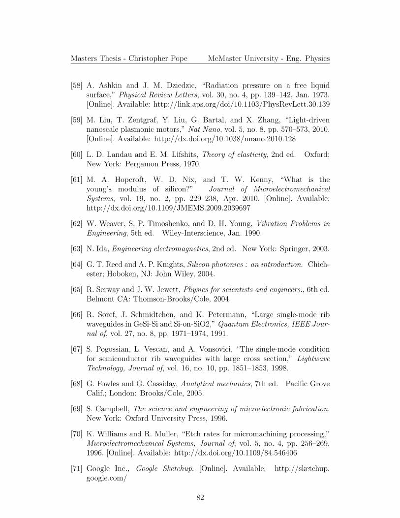
Masters Thesis - Christopher Pope McMaster University - Eng. Physics
[58] A. Ashkin and J. M. Dziedzic, “Radiation pressure on a free liquidsurface,” Physical Review Letters, vol. 30, no. 4, pp. 139–142, Jan. 1973.[Online]. Available: http://link.aps.org/doi/10.1103/PhysRevLett.30.139
[59] M. Liu, T. Zentgraf, Y. Liu, G. Bartal, and X. Zhang, “Light-drivennanoscale plasmonic motors,” Nat Nano, vol. 5, no. 8, pp. 570–573, 2010.[Online]. Available: http://dx.doi.org/10.1038/nnano.2010.128
[60] L. D. Landau and E. M. Lifshits, Theory of elasticity, 2nd ed. Oxford;New York: Pergamon Press, 1970.
[61] M. A. Hopcroft, W. D. Nix, and T. W. Kenny, “What is theyoung’s modulus of silicon?” Journal of MicroelectromechanicalSystems, vol. 19, no. 2, pp. 229–238, Apr. 2010. [Online]. Available:http://dx.doi.org/10.1109/JMEMS.2009.2039697
[62] W. Weaver, S. P. Timoshenko, and D. H. Young, Vibration Problems inEngineering, 5th ed. Wiley-Interscience, Jan. 1990.
[63] N. Ida, Engineering electromagnetics, 2nd ed. New York: Springer, 2003.
[64] G. T. Reed and A. P. Knights, Silicon photonics : an introduction. Chich-ester; Hoboken, NJ: John Wiley, 2004.
[65] R. Serway and J. W. Jewett, Physics for scientists and engineers., 6th ed.Belmont CA: Thomson-Brooks/Cole, 2004.
[66] R. Soref, J. Schmidtchen, and K. Petermann, “Large single-mode ribwaveguides in GeSi-Si and Si-on-SiO2,” Quantum Electronics, IEEE Jour-nal of, vol. 27, no. 8, pp. 1971–1974, 1991.
[67] S. Pogossian, L. Vescan, and A. Vonsovici, “The single-mode conditionfor semiconductor rib waveguides with large cross section,” LightwaveTechnology, Journal of, vol. 16, no. 10, pp. 1851–1853, 1998.
[68] G. Fowles and G. Cassiday, Analytical mechanics, 7th ed. Pacific GroveCalif.; London: Brooks/Cole, 2005.
[69] S. Campbell, The science and engineering of microelectronic fabrication.New York: Oxford University Press, 1996.
[70] K. Williams and R. Muller, “Etch rates for micromachining processing,”Microelectromechanical Systems, Journal of, vol. 5, no. 4, pp. 256–269,1996. [Online]. Available: http://dx.doi.org/10.1109/84.546406
[71] Google Inc., Google Sketchup. [Online]. Available: http://sketchup.google.com/
82

Masters Thesis - Christopher Pope McMaster University - Eng. Physics
[72] E. Ollier, “Optical MEMS devices based on moving waveguides,” IEEEJournal of Selected Topics in Quantum Electronics, vol. 8, no. 1, pp. 155–162, Feb. 2002.
[73] E. Huante-Ceron, “SOI ridge waveguide processing,” McMaster Univer-sity, Unpublished Guide, 2009.
[74] H. Seidel, L. Csepregi, A. Heuberger, and H. Baumgartel, “Anisotropicetching of crystalline silicon in alkaline solutions,” Journal of TheElectrochemical Society, vol. 137, no. 11, pp. 3612–3626, Nov. 1990.[Online]. Available: http://link.aip.org/link/?JES/137/3612/1
[75] Y. Uenishi, M. Tsugai, and M. Mehregany, “Micro-opto-mechanicaldevices fabricated by anisotropic etching of (110) silicon,” Journal ofMicromechanics and Microengineering, vol. 5, pp. 305–312, Dec. 1995.[Online]. Available: http://iopscience.iop.org/0960-1317/5/4/007
[76] D. Taillaert, P. Bienstman, and R. Baets, “Compact efficient broadbandgrating coupler for silicon-on-insulator waveguides,” Optics Letters,vol. 29, no. 23, pp. 2749–2751, Dec. 2004. [Online]. Available:http://ol.osa.org/abstract.cfm?URI=ol-29-23-2749
[77] D. R. Lide, Ed., CRC Handbook of Chemistry and Physics, 92th Edition(Internet Version 2011), 92nd ed. Boca Raton, FL: CRC Press/Taylorand Francis, 2011. [Online]. Available: http://www.hbcpnetbase.com
[78] A. Cowen, G. Hames, D. Monk, S. Wilcenski, and B. Hardy,“SOIMUMPs design handbook,” MEMSCAP Inc., Tech. Rep., 2011,revison 8.0. [Online]. Available: http://www.memscap.com/products/mumps/soimumps/reference-material
[79] A. Rampal, “Experimental and theoretical study of quartz and InPpiezoelectric MEMS resonators,” Master’s Thesis, McMaster University,Hamilton, Ontario, 2009.
[80] J. Wei, C. Yue, Z. L. Chen, Z. W. Liu, and P. M. Sarro, “A siliconMEMS structure for characterization of femto-farad-level capacitivesensors with lock-in architecture,” Journal of Micromechanics andMicroengineering, vol. 20, no. 6, p. 064019, Jun. 2010. [Online].Available: http://iopscience.iop.org/0960-1317/20/6/064019
[81] CadSoft Computer, EagleCAD. [Online]. Available: http://www.cadsoftusa.com/
83

Masters Thesis - Christopher Pope McMaster University - Eng. Physics
[82] J. Ardizzoni, “A practical guide to High-Speed Printed-Circuit-Boardlayout,” Analog Dialog, vol. 39, no. 3, Sep. 2005. [Online]. Available: http://www.analog.com/library/analogDialogue/archives/39-09/layout.html
[83] S. Guinta, “Ask the applications engineer - 21: Capacitance andcapacitors,” Analog Dialog, vol. 30, no. 2, 1996. [Online]. Available:http://www.analog.com/library/analogDialogue/Anniversary/21.html
[84] Andeed-Hagerling Inc, 2500A 1kHz Ultra-Precision Capacitance BridgeManual, Cleveland, Ohio.
[85] Amptek Inc., A250 Charge Sensitive Preamplifier Datasheet, Bedford,MA. [Online]. Available: http://www.amptek.com/a250.html
[86] Stanford Research Systems, Model SR844 RF Lock-In AmplifierUser’s Manual, Sunnyvale, California, 2007. [Online]. Available:http://www.thinksrs.com/downloads/PDFs/Manuals/SR844m.pdf
[87] Stanford Research Systems, “About Lock-In amplifiers,” ApplicationNote. [Online]. Available: http://www.thinksrs.com/support/app.htm
[88] National Instruments Corporation, LabVIEW 8.2. [Online]. Available:http://www.ni.com/labview/
84