Embed Size (px)
Citation preview
University of South Florida University of South Florida
Scholar Commons Scholar Commons
Graduate Theses and Dissertations Graduate School
2005
Development of a CTD System for Environmental Measurements Development of a CTD System for Environmental Measurements
Using Novel PCB MEMS Fabrication Techniques Using Novel PCB MEMS Fabrication Techniques
Heather Allison Broadbent University of South Florida
Follow this and additional works at: https://scholarcommons.usf.edu/etd
Part of the American Studies Commons
Scholar Commons Citation Scholar Commons Citation Broadbent, Heather Allison, "Development of a CTD System for Environmental Measurements Using Novel PCB MEMS Fabrication Techniques" (2005). Graduate Theses and Dissertations. https://scholarcommons.usf.edu/etd/2795
This Thesis is brought to you for free and open access by the Graduate School at Scholar Commons. It has been accepted for inclusion in Graduate Theses and Dissertations by an authorized administrator of Scholar Commons. For more information, please contact [email protected].

Development of a CTD System for Environmental Measurements Using Novel PCB
MEMS Fabrication Techniques
by
Heather Allison Broadbent
A thesis submitted in partial fulfillment of the requirements for the degree of
Master of Science College of Marine Science University of South Florida
Major Professor: David A. Mann, Ph.D. Norman J. Blake, Ph.D.
Andres M. Cardenas-Valencia, Ph.D. Eric T. Steimle, Ph.D.
Date of Approval: November 7, 2005
Keywords: microsensors, salinity, conductivity, temperature, liquid crystal polymer, microfabrication
© Copyright 2005, Heather Allison Broadbent

To my father
for always being there
AKNOWLEDGEMENTS
I am appreciative of the Office of Naval Research (Grant N00014-03-1-0480) for
funding for this research. Thanks also go to Stan Ivanov of the USF College of Marine
Science Center for Ocean Technology for electrical engineering contributions, to Chad
Lemke and Mark Holly for their mechanical engineering contributions, to David Edwards
for providing the 3D surface topography measurements, to Carl Biver of the USF
Chemistry Department for his statistical contributions, to Joe Kolesar, Charles Jones and
Nghia Huynh for their technical support.
I would like to express my gratitude to David Fries and George Steimle for their
support, instruction, discussions, and encouragement. Without their contributions, this
work would not have been possible.
I especially thank my committee, David Mann, Ph.D., Norman Blake, Ph.D.,
Andres Cardenas-Valencia, Ph.D., Eric Steimle, Ph.D., for all of their continued support,
technical contributions and encouragement. I am honored to have them as mentors.
And finally, I am ever grateful to my husband, Russell, my father and my sister,
for their continued support. I owe all of my achievements to them.

TABLE OF CONTENTS
LIST OF TABLES iii
LIST OF FIGURES iv ABSTRACT vii CHAPTER I. INTRODUCTION 1 Background on CTD Instruments 1 Traditional Microfabrication Techniques 7 Motivation and Scope of Thesis 9 CHAPTER II. DEVELOPMENT OF NOVEL MICROFABRICATION TECHNIQUES 11
Maskless Photolithographic Patterning Tool 11
Liquid Crystal Polymer Material 14 Lamination 15 Etching 15
Metallization 15 Novel PCB MEMS Microfabrication Techniques 18 CHAPTER III. SENSOR DEVELOPMENT AND SYSTEM INTEGRATION 20 Conductivity Cell 20
Design 20 Novel Fabrication Process 27
Resistive Temperature Device 34 Design 34 Novel Fabrication Process 37
Depth Sensor 39 CTD System Integration 40
Underwater Packaging 42 CTD System Description 45 Electronics 45 Output 45
i

Logging 45 Power 46 Software 46 CHAPTER IV. RESULTS AND DISCUSSION 48 Conductivity Cell 48 Calibration and Statistical Evaluation 48 Comparison Test 55 Resistive Temperature Device 58 Calibration and Statistical Evaluation 58 Comparison Test 62 Depth Sensor 65 Comparison Test 65 System Evaluation 67 Field Test 72 CHAPTER V. CONCLUSIONS 75 Summary 75 Future Research 77 REFERENCES CITED 78
ii

LIST OF TABLES
Table 1. Commercially Available CTD Instruments 2 Table 2. LCP Physical Properties 17
Table 3. Average values of Conductivity and Conductance with Standard 53
Deviation
iii

LIST OF FIGURES
Figure 1. Excell 2” Micro CTD, Falmouth Scientific, Inc 5 Figure 2. Micro CTD, Applied Microsystems LTD 5 Figure 3. Maskless photolithographic patterning tool 12 Figure 4. PCB MEMS process using LCP 19 Figure 5. Schematics of the conductivity cell (A. Front, B. Back) 21 Figure 6. Conductivity cell rings with measurements 22 Figure 7. Block diagram of the conductivity circuit 24 Figure 8. Conductivity cell process sequence 28 Figure 9. LCP 3D surface topography measurement before micro-etch 29 Figure 10. LCP 3D surface topography measurement after micro-etch 29 Figure 11. Dark field artwork for conductivity cell (A Front, B Back) 31 Figure 12. (A) conductivity cell electrode rings, (B) conductivity cell electrodes 33 Figure 13. Light field artwork for resistive temperature device 35 Figure 14. RTD traces magnified 4x with measurements 35 Figure 15. Block diagram of the temperature circuit 36 Figure 16. Photo of resistive temperature device (26 mm x 10 mm) 38 Figure 17. Piezoresistive pressure sensor (7.3 mm diameter), Intersema 39
Figure 18. Depth sensor circuit board (19 mm x 10 mm) 40
Figure 19. Sensor plugs mounted to end cap 43 iv

Figure 20. Miniature CTD system prototype 44
Figure 21. Menu format of the CTD system 47
Figure 22. Conductivity cell calibration curve with 95% confidence limits 51
Figure 23. Residual plot for conductivity curve and repeated runs 52
Figure 24. Plotted data points of conductivity cell replicates of measured 54
conductance vs. calculated conductivity
Figure 25. Mettler Toledo conductivity probe vs. fabricated conductivity cell 56
Figure 26. Measured conductivity for conductivity cell vs. Mettler Toledo 57 probe
Figure 27. Difference calculated between commercial probe and conductivity cell 57
Figure 28. Resistive temperature device calibration curve with 95% confidence 59
limits
Figure 29. Temperature calibration curve and 4 additional runs 60
Figure 30. Residual plot of temperature data set 60
Figure 31. 95% Prediction Intervals 61
Figure 32. Commercial digital thermometer vs. RTD 63
Figure 33. RTD and commercial digital thermometer data plotted against 63
calibrated thermometer.
Figure 34. Difference in 0C for measured temperature between RTD and 64
commercial digital thermometer.
Figure 35. Comparison graph of Intersema vs. Keller pressure sensors 66
Figure 36 Keller pressure sensor vs. Intersema pressure sensor 66
Figure 37. CTD system evaluation plot 69
v

Figure 38. Twenty-four hour evaluation CTD test with measured conductivity, 70
temperature and depth
Figure 39. Salinity values for given mS/cm and temperatures 71
Figure 40. Field test data of the CTD measurements with water level 74
vi

Development of a CTD System for Environmental Measurements Using Novel PCB MEMS Fabrication Techniques
Heather Allison Broadbent
ABSTRACT
The development of environmental continuous monitoring of physicochemical
parameters via portable small and inexpensive instrumentation is an active field of
research as it presents distinct challenges. The development of a PCB MEMS-based
inexpensive CTD system intended for the measurement of environmental parameters in
natural waters, is presented in this work. Novel PCB MEMS fabrication techniques have
also been developed to construct the conductivity and temperature transducers. The
design and fabrication processes are based on PCB MEMS technology that combines Cu-
clad liquid crystal polymer (LCP) thin-film material with a direct write photolithography
tool, chemical etching and metallization of layers of electroless nickel, gold, and
platinum. The basic principles of a planar four-electrode conductivity cell and the
resistive temperature device are described here as well as the integration and the
packaging of the microfabricated sensors for the underwater environment. Measurement
results and successful field evaluation data show that the performance of the LCP thin-
film microsensors can compete with that of conventional in-situ instruments.
vii
CHAPTER I
INTRODUCTION
Background on CTD Instruments
Salinity is one of the primary measurements to be determined by oceanographers
when analyzing a sample of seawater. By determining salinity, researchers can calculate
numerous other important properties of seawater, such as density, conservative element
concentrations, and solubility of gases (Pilson, 1998). Also, salinity affects functional
and structural properties of organisms through changes in total osmotic concentration,
relative proportions of solutes, coefficients of absorption and saturation of dissolved
gases, density and viscosity (Kinne, 1964). Salinity measurements provide relevant
information to all fundamental fields of oceanography including chemical, biological,
physical and geological. For instance, in the biological arena, salinity has been correlated
to the upstream distribution of species within estuaries (Wells, 1961). Also, salinity data
have provided geologists with information about carbonate building organisms (Heckel,
1974). Since the 1960’s, oceanographers have determined salinity based on comparative
measurements of electrical conductivity with instruments called salinometers in place of
the earlier titrimetric determination of chlorinity (Farland, 1975). In the early 1970’s,
these instruments evolved into reliable, accurate, field-deployable devices due to the
advancement of microprocessor technology. They are currently able to measure
1

conductivity ratios with an accuracy of +/- 0.001 Siemens (Pilson, 1998). Because these
in-situ instruments not only measure conductivity, but also temperature and depth, they
are now referred to as CTD instruments. The three in-situ measurements are used in an
algorithm to calculate salinity based upon the Practical Salinity Scale 1978 (PSS 1978)
(Lewis, 1980). Many different CTD models are commercially available that range in size
and cost (Table 1).
Table 1. Commercially available CTD instruments
Manufacturer Conductivity Temperature Size Cost
Range [mS/cm]
Accuracy [mS/cm]
Range [0C]
Accuracy [0C] [Inches] $
Falmouth 0-70 +/- 0.005 -5 to 36 +/- 0.002 12 x 2 10,000+
Applied Microsystems 0-70 0.005 -2 to 32 +/- 0.002 20 x 2 6,900+
Ocean Sensors 0.5-65 0.02 (FS) -2 to 32 0.01 28 x 2.5 7,000+
Sea-Bird 0-90 0.003 -5 to 35+ 0.002 25 x 2.5 8,000+
InterOcean Systems 0.5-60 +/- 0.05 -5 to 45+ +/- 0.02 7 x 5 8,500+
RBR 0- 70 +/- 0.003 -5 to 35 +/- 0.002 16 x 2.5 4,000+
Conductivity, temperature and depth measurements can be acquired using several
types of sensors or transducers. Inductive-style conductivity sensors usually consist of
two high- grade toroids or coils which are incorporated concentrically and adjacent to
each other. The coils form a current transformer. As the conductive liquid media flows
2

past the toroids, it forms a closed conductive field path. When voltage is applied to the
primary coil it causes a current flow that is proportional to the conductivity of the sample
medium. Another type of conductivity sensor is the electrode cell, which is typically
constructed of platinum metal rings or bars with a known cell constant. When they are
immersed within a conductive liquid medium and a known voltage is applied, the
conductivity of the fluid is proportional to the measured current across the two electrodes.
Inductive sensors have an advantage over those with electrodes, as electrodes are
adversely affected by polarization and fouling (Dauphinee, 1981), although an
appropriate surface conditioning treatment has been shown to improve the polarization
characteristics of planar electrode cells (Jacobs et al., 1990).
Resistive temperature devices (RTD) are metallic sensors (platinum or copper) in
which the metal’s resistance increases with increasing temperature in a known and
repeatable manner. A thermocouple consists of two dissimilar metal wires welded
together into a sensing junction with a reference junction at the other end of the signal
wires. A thermoelectric potential proportional to the temperature difference between the
two junctions is generated when the sensing junction is heated. This potential indicates
the temperature at the sensing junction, when compensation is made for the known
temperature of the reference junction. Of the two, RTD sensors have the advantage in
environmental monitoring due to fact that they produce the best linearity and are
extremely stable, whereas thermocouples are best suited for extreme conditions of high
temperatures.
Depth is calculated from pressure, water compressibility, and latitude. The
piezoelectric pressure sensor is one type of transducer used in oceanographic CTD
3

instruments. The sensor consists of a pressure-sensing diaphragm that transduces the
force to a stack of discs made of piezoelectric ceramics or crystalline quartz. The
electrical charges produced are proportional to the pressure. Another pressure sensor
used to measure depth is the strain gauge. The strain gauge consists of a metal foil
pattern that is distorted when force is applied, resulting in a change in the resistance.
Piezoelectric pressure sensors have the advantage of inherent static accuracy and offer
excellent long-term stability, whereas the strain gauge is moderately accurate and long-
term stability is an issue (Matthews, 2005).
A major trend in CTD development is miniaturization, which not only impacts the
instrument’s size and weight, but also its cost (Brown, 1991). Miniaturization of
electrical components, microprocessors and memory chips by technological advances in
microfabrication techniques and materials enables the development of very small
oceanographic CTD systems capable of continuous monitoring that are rapid, reliable and
cost effective (Madou, 1997). Miniaturization of the CTD will impact the oceanographic
community greatly by (1) increasing the range of applications by allowing in situ
measurements of dynamic physical, chemical, and biological properties over varying
temporal and spatial scales, and (2) reducing the cost per unit thus allowing greater
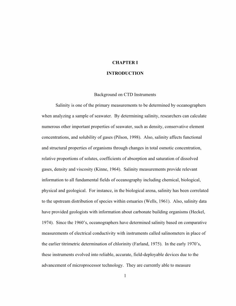
accessibility to researchers. Woods Hole Oceanographic Institute (WHOI) and ocean
instrument manufacturer, Falmouth Scientific Instruments (Cataumet, MA.), have
collaborated to develop very small (12 inches x 2 inches), low cost ($10,000), deployable
CTD systems (Figure 1). Applied Microsystems (Sidney, BC, Canada) has introduced a
Micro CTD instrument for measuring salinity, which is 20 inches long by 2 inches wide
(Figure 2).
4
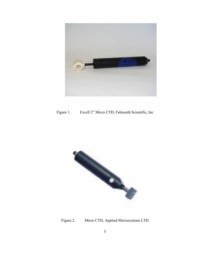
Figure 1. Excell 2” Micro CTD, Falmouth Scientific, Inc
Figure 2. Micro CTD, Applied Microsystems LTD
5

Other CTD research has focused on high performance coupled with low power for
long-term deployment applications (Brown, 1994). CTD research has also been
conducted on instruments that are capable of long-term deployments in biologically
active ocean regions (Fougere, 2000). Some research has been conducted to develop a
microcomputer-controlled, expendable CTD profiler that is launched from aircraft
(Downing et al., 1992).
A miniature, low cost CTD provides scientists with a powerful analytical
instrument that can be integrated into many types of research systems. For example, this
sensor system can be coupled with autonomous underwater vehicles (AUV), remotely
operated vehicles (ROV), interconnected arrays that concurrently collect data profiles, or
tracking salinity profiles of marine organisms of all sizes.
6

Traditional Microfabrication Techniques
Sensors and microsystems, such as those used by CTD instruments are created by
microfabrication techniques. Traditional microfabrication starts with photolithography,
which is the technique used to transfer copies of a master pattern onto the surface of a
substrate material. A photomask of the desired pattern is generated using either film
acetate and emulsion or optically flat glass with a metal (e.g., chromium) absorber
pattern. The absorber pattern on the photomask blocks ultraviolet light, whereas the film
acetate or glass is transparent to UV. The photomask is placed directly on the photoresist
coated substrate, and is exposed to ultraviolet radiation using a UV light box, thus
creating a 1:1 image of the pattern. Since these masks make physical contact with the
substrate, they have the tendency to degrade over time due to wear. This degradation
limits the lifespan of the mask (Madou, 1997). [A light field or dark field image can be
generated on the photomask that is dependent upon the type of photoresist is used for
pattern transfer.] The photoresist is a polymer that changes structure when exposed to
radiation. It is applied to the surface of the substrate either by spinning or lamination.
There are two types of photoresists, positive and negative. Positive photoresists have
polymer chains that become weakened when exposed to UV radiation, thus causing the
resist to become more soluble in developing solutions. Negative photoresists are
strengthened by cross-linkage caused by UV exposure, thus becoming less soluble.
Several factors dictate which type of resist to use, such as pattern feature size,
photospeed, adhesion to substrate, thermal stability, and wet chemical resistance (Madou,
1997). Once the pattern has been transferred onto the surface of the substrate via
photomask and UV radiation, a developer is used to create a relief image in the
7

photoresist. This relief image serves as a mask during other additive and subtractive
processes such as etching and metallization.
Traditional microfabrication of sensors and devices uses silicon wafers as a
substrate (Sheats and Smith, 1998). The silicon wafer has the ability to conduct
electricity in a very controlled manner, making it an ideal substrate for the construction of
most advanced semiconductor devices.
8

Motivation and Scope of Thesis
The motivation of this work was to develop a miniature, low cost CTD system
using novel PCB MEMS fabrication techniques combined with liquid crystal polymer
(LCP) material that measures salinity in natural waters. By using a novel
photolithography technology developed at COT, combined with LCP material, it is
possible to rapidly produce expendable conductivity and temperature microsensor
prototypes that can be easily reconfigured for extensive experimentation, thus allowing
quick development and mass quantity fabrication of ocean sensors (Fries et al., 2002).
The main scope of this work addresses two important milestones in conductivity
and temperature sensors. The first milestone was construction of LCP-based conductivity
and temperature sensors using novel PCB MEMS fabrication techniques without an
expensive cleanroom environment. The second was miniaturization of the sensors.
Small sensor size increases the range of applications from open-ocean profiling to
monitoring microscale processes. The combination of these factors ultimately lead to the
production of low-cost sensors, thereby allowing greater accessibility to the scientific,
academic, public and private communities. These milestones led to the design of a planar
thin-film four-electrode conductivity cell and a thin-film copper resistive temperature
device.
Once the two microsensors were fabricated and tested in the laboratory, they were
then combined with a commercially available piezoresistive pressure sensor to produce
the entire CTD system. Along with the development and fabrication of the sensors, the
integration and packaging of the CTD system in a watertight housing for the marine
environment was investigated and developed in this work. Once the CTD system was
9

packaged, the sensors were calibrated, and field-tests were performed. Field deployment
of the completed CTD system was performed in Bayboro Harbor, St. Petersburg, Florida.
Oceanographic researchers are exploring various new tools, such as instrumented
animals, in order to study the physical, chemical and biological structure of the oceans,
(Boehlert et al., 2001). Salinity measurements acquired from these autonomous
environmental samplers (pinnipeds, cetaceans, fishes) is of interest to oceanographers
investigating density structure and mixed layer depth (Freeland et al., 1997). However,
limitations in the size and cost of CTD instruments have prohibited the extensive
collection of salinity data by this method (Hooker and Boyd, 2003). The development of
small, expendable, inexpensive CTD systems would be beneficial in the collection of
salinity data sampled using autonomous biological vehicles, thus providing scientists
with an additional data source.
10

CHAPTER II
DEVELOPMENT OF NOVEL MICROFABRICATION
TECHNIQUES
Maskless Photolithographic Patterning Tool
As stated previously, traditional microfabrication techniques involve photomasks
generated from film acetate or glass with an absorber pattern. These photomasks have
limited usage duration due to damage that results from physical contact with the substrate
and operator. The pattern on the mask has a tendency to become scratched and therefore
no longer viable for the application. The Center for Ocean Technology Systems Group
developed a tool that replaces the physical photomask with a projected UV photomask
(Figure 3). This tool (SF-100), has been licensed by Intelligent Micro Patterning LLC,
St. Petersburg, Florida.
The maskless photolithographic patterning tool technology utilizes reflective
micro optics in combination with mixing and imaging lenses to allow direct circuit image
projection onto a substrate surface. In this technique, reflective
microoptoelectromechanical (MOEM) elements are used to spatially modulate light such
that light can be controlled on the several micron-sized regime, simultaneously over a 13
mm x 10 mm sized field of view. The desired pattern is designed and stored using
conventional computer-aided drawing tools and is used to control the positioning of the
11
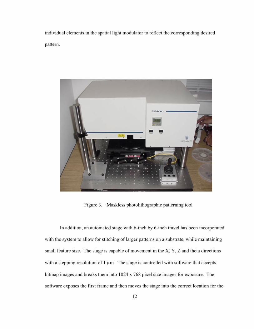
individual elements in the spatial light modulator to reflect the corresponding desired
pattern.
Figure 3. Maskless photolithographic patterning tool
In addition, an automated stage with 6-inch by 6-inch travel has been incorporated
with the system to allow for stitching of larger patterns on a substrate, while maintaining
small feature size. The stage is capable of movement in the X, Y, Z and theta directions
with a stepping resolution of 1 µm. The stage is controlled with software that accepts
bitmap images and breaks them into 1024 x 768 pixel size images for exposure. The
software exposes the first frame and then moves the stage into the correct location for the
12

next exposure of the pattern. The tool’s shutter is also controlled by the stage software
and once programmed the stage will automatically expose the entire pattern, thus
allowing the user to do other tasks.
This patterning tool, by eliminating the use of traditional contact photomasks,
provides distinct photolithographic advantages over conventional methods. Once the
pattern has been designed using the desired software, it can be changed and manipulated
in much less time than required to generate a traditional photomask. Pattern changes can
be performed from seconds to minutes. This allows for rapid generation of numerous
prototypes. Traditional photomasks must be filed and stored in a clean, temperature and
humidity controlled environment. The patterns generated for the maskless tool are
electronically stored in a memory file on a computer, thus eliminating mask
contamination and the need for proper storage space. The maskless photolithographic
tool eliminates the need for photomask generating tools such as cameras, printers and
harsh chemicals, along with the separate UV exposure unit. Low cost microsensors and
microsystems can be fabricated rapidly by using the novel maskless photolithographic
tool.
13
Liquid Crystal Polymer Material
Liquid crystal polymer (LCP) is a thermoplastic dielectric material developed
specifically for single layer and multilayer substrate constructions with unique structural
and physical properties. The polymer contains rigid and flexible monomers that link
together. Once in the liquid state, the rigid monomers align next to each other in the
direction of shear flow. When this orientation is formed, the structural alignment of
monomers persists, even after the LCP has cooled below melting temperature (Jayaraj
and Farrell, 1998). As a result of this unique structure, LCP exhibits a combination of
electrical, thermal, mechanical and chemical properties that other polymers do not. LCP
material is characterized by low and stable dielectric constant and dielectric loss (0.004).
LCP has good dimensional stability and low modulus, allowing it to bend easily for flex
and contour applications. LCP has extremely low moisture absorption (0.04%) and low
moisture permeability, which allows the material to maintain stable electrical, mechanical
and dimensional properties in humid environments. LCP has very high chemical
resistance and is unaffected by most acids, bases and solvents (Culbertson, 1995). The
combination of these physical properties make LCP material well suited for underwater
sensor applications (Table 2).
LCP material is commercially supplied in a predefined thickness ranging from 25
µm to 3 mm. The material may have an 18 µm thick copper cladding layer laminated to
one or both sides. In this work, 200 µm thick (8 mil), double-copper clad LCP material
was supplied by Rogers Corporation, AZ.
14

Lamination
The fabrication of PCB MEMS devices and sensors can be achieved with LCP
material. A lamination process has been developed that allows the LCP to be thermally
bonded to MEMS materials. With the correct applied temperature and pressure, the
material will flow and bond to another layer of LCP as well as to other materials such as
glass, copper, gold or silicon (Wang et al., 2003). This lamination process allows thicker
(0.008 inch) LCP material to be produced, which can be used to fabricate more rigid
layers or microsensors. It also allows the fabrication of complex multi-layer, three-
dimensional structures.
Etching
Even though LCP is highly chemical resistant, it is possible to chemically attack
and dissolve the material. By using a strongly alkaline, caustic solution (KOH @ 90 0C),
LCP can be surfaced etched or completely dissolved. When this process is combined
with PCB MEMS techniques, it is possible to fabricate microfluidic channel devices and
metallized microsensors. LCP material has been surfaced etched using a reactive ion
etching (RIE) process. This process utilizes an oxygen plasma RIE machine that
increases the surface roughness of the LCP material (Wang et al., 2003).
Metallization
LCP material can be metallized using several different processes such as
lamination, resistive evaporation and electrodeposition. Generally, the LCP material is
clad with 18 µm thick copper. This copper layer is laminated to one or both sides of the
15
LCP material using a vacuum press at a temperature around the melting point of the
polymer material (Jayaraj and Farrell, 1998). Wang et al. (2003) has evaporated
aluminum onto LCP to serve as an etch mask. In this work, an electrodeposition process
that produces additive metal structures (nickel) above the LCP surface is discussed. This
process, commonly used for printed circuit board material such as FR4 (fiberglass),
allows the deposition of a large number of metals, such as Au, Ag, Cu, Ni, Pt, Pd… etc,
to be electroplated to the surface of the material once a Pd seed layer has been
catalytically deposited (Kovacs, 1998).
16
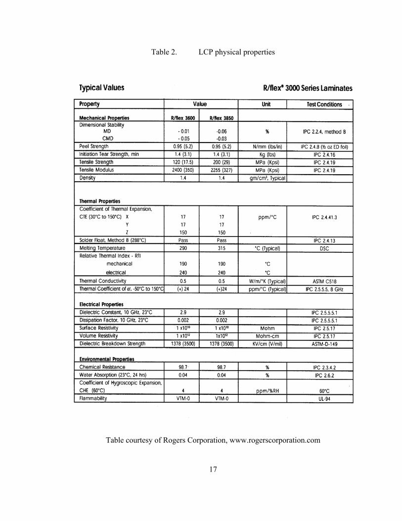
Table 2. LCP physical properties
Table courtesy of Rogers Corporation, www.rogerscorporation.com
17

Novel PCB MEMS Fabrication Techniques
In recent years, there has been considerable interest in the development of
microelectromechanical systems (MEMS) fabricated with printed circuit board
processing techniques (Ramadoss et al., 2003). The advantages of the PCB MEMS based
approach include low cost, suitability for batch fabrication, ease of integration with
electronics, and high volume manufacturing (Palasagaram et al., 2005). The use of liquid
crystal polymer has emerged recently as a suitable substrate for MEMS, replacing silicon.
LCP’s low cost, flexible fabrication and packaging techniques, and physical and chemical
properties, not available in silicon materials, allow large arrays of conductivity and
temperature sensors to be fabricated using roll-to-roll flexible printed circuit processing
systems for large area applications (Wang et al., 2003).
In the past, planar conductivity sensors have been fabricated using alumina or
quartz glass substrates. Farrugia and Fraser (1984) have used a multi-layer screening
technique for fabrication of a conductivity cell using alumina. Norlin et al. (1998) used
micromachining and MEMS techniques for fabrication of planar Pt conductivity
electrodes and Pt thermistors using quartz glass wafer. In this work, novel LCP material
is combined with the maskless photolithographic tool to fabricate PCB MEMS-based
conductivity and temperature sensors.
Figure 4 illustrates the novel PCB MEMS process used to fabricate the two
oceanographic sensors. The process steps include photoresist application, maskless
pattern exposure, pattern development, and etching of copper and/or LCP material. This
process allows the construction of the desired architectures used to fabricate sensors such
18

as through holes and blind vias. This novel microfabrication technique (figure 4) allows
for the rapid construction of a cost effective miniature CTD system.
Figure 4. PCB MEMS process using LCP
19

CHAPTER III
SENSOR DEVELOPMENT AND SYSTEM INTEGRATION
Conductivity Cell
Design
The conductivity sensor design was a planar, thin film, four-electrode cell (Figure
5). It consists of four metallic rings plated to a LCP substrate. The rings consist of three
metal layers: electroless nickel, electroless gold and platinum black, respectively. The
electroless nickel exhibits uniform thickness and low porosity, thus making it an effective
corrosion-protection agent against seawater (Schlesinger and Paunovic, 2000). The thin
electroless gold layer improves the adhesion of the platinum black. The porous platinum
black layer finalizes the construction, which increases the surface area and reduces the
metal to seawater interfacial polarization impedances (Jacobs et al., 1990). Traces (on
the backside) then run to contact points under each of the four rings, where plated thru-
holes were made to connect the traces to the rings. The holes are within the geometry of
each ring and do not interfere with the cell. Electrical contact fingers were attached to
the traces to connect the circuit to the sensor circuit board (figure 5B). The circuit and
contact fingers were also plated with electroless nickel and gold simultaneously with the
conductivity electrodes. The gold layer makes an excellent electrical conductor for the
circuit.
20

(A)
(B)
Figure 5. Schematics of the conductivity cell (A. Front, B. Back)
21

The overall diameter of the conductivity sensor was approximately 10 mm. The three
outermost rings are approximately 310 µm with a distance of 665 µm between them. The
center ring has an approximate diameter of 4 mm. Figure 6 shows a magnified (4x)
section of the conductivity cell rings with their measured widths.
Figure 6. Conductivity cell rings with measurements
Rings 1 and 4 are the drive rings while rings 2 and 3 are the sense rings (Figure
5A). Current flows through the two drive rings (ring 1 and ring 4), while the voltage
drop is sensed by the two inside rings (ring 2 and 3). The cell excitation is an alternate 22

current (AC) signal that is produced by a Wein bridge oscillator. The oscillator runs at
10 kHz, but its feedback circuitry allows the amplitude to be controlled by a direct
current (DC) signal from the microcontroller’s digital to analog (D/A) converter. The AC
signal remains at a constant amplitude and is applied as an AC voltage across the drive
rings. To eliminate the need for split supplies for the electronics, the signal is shifted up
by adding 2.5V DC. No DC potential can be present in the cell since corrosion and
calcium deposits will destroy it promptly. Thus, the signal is low pass filtered and the
DC potential is applied to the inside ring, while the shifted AC is applied to the outside
ring. There are extra connections to the current carrying rings that allow the user to
observe any losses in the connection to the sensor itself, and the amplifier circuitry uses
that as part of the feedback such that the exact signals are applied to the rings. The
current required for the cell is applied through a current sensing resistor before the
feedback, so the resistor does not form part of the sensor, but rather part of the driving
circuit. The voltage drop across the resistor is then fed to a precision peak detector and
then buffered. The current is derived using the formula:
Icell = Vpeak/ Rref [1]
Vpeak = Voltage peak measured
Rref = Resistance (Reference)
23

Figure 7. Block diagram of the conductivity circuit
Since the amplitude of the voltage used for the cell excitation and the current
required to drive the potential are known, the conductance (Siemens) of the cell can
easily be calculated using the formula:
S= I/V [2]
S= Siemens (amps/volts)
I= Current (amps)
V= Voltage (volts)
24

Possible problems with the sensor are biofouling, biofilming, corrosion and/or
mineral deposition of the sensor that can change the geometry of the field, increase
contact resistance, and reduce the contact area. Biofouling and biofilming of the
conductivity cell can be caused by sea surface oils, bacterial colonies and marine
organisms that adhere to the electrodes (Varney, 2000). The current carrying electrodes
are the most vulnerable to this sort of damage, while the voltage sensing electrodes will
most likely have to withstand only salt effects. Therefore, they are hooked up to a
differential amplifier with very low input bias current, which is also fed to a buffered
peak detector, such that we now have a 3rd feedback point for measurements. As the
sensor becomes corroded, a difference would become observable between the voltage
sensing rings and the programmed AC signal, such that we could predict the state of the
sensor over time.
Due to the constant potential biasing scheme, the sensor can measure salinities
down to DI water levels, as well as the full range up to 70mS/cm. The resolution across
the entire range remains unchanged, while maintaining a linear response. By using the
programmed AC potential and the current measurements, a volume measurement is
made, which encompasses the water up to 1mm from the surface of the electrodes. When
fouling begins to affect the current carrying electrodes, this method could potentially
begin to exhibit higher order responses. In this case, the voltage measurement electrodes
can be used to replace the programmed AC potential in the conductance equation since
they will not be subject to deterioration affecting their geometry. This will yield a surface
measurement that affects only the primary ion path. However, this method is more
accurate at higher conductivities since more current paths are created away from the
25

surface of the cell by the increasing ion concentration. To achieve maximum resolution,
the two calibration models can be used, where the micro controller can select the right
one based on the current range.
26

Novel Fabrication Process
The conductivity cell was fabricated using PCB MEMS techniques combined
with the maskless photolithographic tool and 8-mil thick double copper-clad liquid
crystal polymer material. An overview of the process sequence is shown in figure 8. The
first step of the process was to clean the surface of the copper clad LCP material with a
sodium persulfate solution for 1 minute. This solution performs a micro-etch of the
surface by removing a thin layer of copper, thus exposing a clean, dull layer. Next, the
copper surface of the LCP was laminated with a negative dry-film photoresist (Dupont
950) and exposed for 9 seconds with the conductivity cell contact pad pattern (backside)
using the maskless photolithographic tool. After development of the photoresist (NaCO3,
1%, 1 minute), the pattern was used as a template to drill the five thru-holes. The thru-
holes bridge the conductivity cell rings (front side of sensor) to the electrical contact pads
and fingers (backside of sensor). Once the thru-holes were drilled, the copper was
entirely etched away using sodium persulfate (approximately 6 minutes) and then the
LCP was uniformally micro-etched for 5 to 10 minutes in a KOH solution (32%, 20%
ethanolamine, 900C) to roughen the surface for metallization (Technic and Crane ECIT).
After the micro-etch, the surface of the etched LCP material was examined and measured
against the surface of a non-etched piece of LCP using a Veeco Wyco NT 3300 Optical
Profiler (Figure 9 and Figure 10). The Ra measurements resulted in a difference in
surface area from 913.80 nm (before micro-etch) to 955.88 nm (after micro-etch). The
images produced show a change in surface topography where the etched piece has a
rougher surface compared to the non-micro-etched piece. Also the LCP thickness was
27

measured before (0.00845 inch) and after (0.00790 inch) the micro-etch resulting in a
0.00055 inch loss of surface material.
Figure 8. Conductivity cell process sequence
28

Figure 9. LCP 3D surface topography measurement before micro-etch
Figure 10. LCP 3D surface topography measurement after micro-etch 29

After the micro-etch, the LCP substrate was catalyzed for metallization. The catalysation
deposition process (Shipley, Marlborough, MA) involves several steps:
1) Cleaner (3320) 5 minutes
2) Deionized Water Rinse 1 minute
3) Deionized Water Rinse 1 minute
4) Pre-dip (Cataposit 404) 1.5 minutes
5) Catalyst (Cataposit 44) 5 minutes
6) Deionized Water Rinse 1 minute
7) Deionized Water Rinse 1 minute
8) Deionized Water Rinse 1 minute
9) Accelerator (Accelerator 19) 6 minutes
10) Deionized Water Rinse 1 minute
Once the LCP was catalyzed with the palladium solution (Cataposit 44), it was plated
with a thin-film (0.4 microns) of electroless nickel (Enthone 425, West Haven, CT) at
90 0C for 2 minutes. After the deposition of electroless nickel, Dupont 950 photoresist
was laminated to the front and back of the nickel-plated LCP substrate. Then the
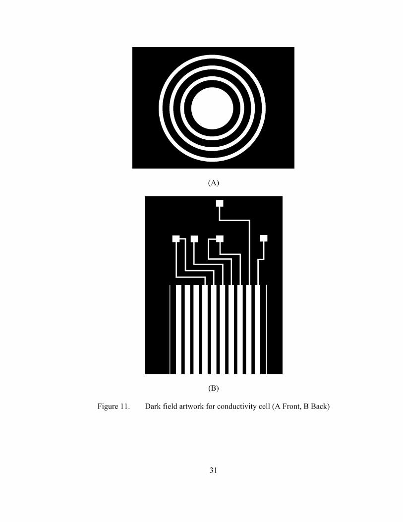
electronically generated conductivity cell patterns (figure 11) were exposed onto the
surface using the maskless photolithographic tool. The exposure time used was 9
seconds. The circuit with contact fingers was exposed first to insure proper registration
for the plated thru-holes. This pattern was a two-step exposure. Then the substrate was
turned over and the cell rings were exposed.
30
(A)
(B)
Figure 11. Dark field artwork for conductivity cell (A Front, B Back)
31

After pattern exposure, the images were developed for 1 minute using NaCO3 (1%)
(Fisher Scientific, Pittsburg, PA). After development, the excess nickel was etched away
using an aqua regia solution (66% HCl, 33% HNO3, Fisher) for 60 seconds, leaving the
desired pattern in the thin plated nickel. The conductivity cell pattern was cleaned in an
acid dip solution (HCl 20%) for 2 minutes and re-deposited with 25- micron thick layer
of electroless nickel (Enthone 425, 2 hours). Once the nickel metal was built up, a thin
layer of electroless gold (Bright Electroless Gold, Transene, Danvers, MA) was
chemically deposited for 10 minutes. Then a porous layer of platinum black metal
(Yellow Springs Instruments, Yellow Springs, OH) was deposited using a current density
of 0.1 A/cm 2 For 5 minutes (Gileadi et al., 1975) (Figure 12).
32

(A)
(B)
Figure 12. (A) conductivity cell electrode rings, (B) conductivity cell electrodes
33

Resistive Temperature Device
Design
The temperature sensor designed was a linear resistive temperature device
(RTD), which is a thin film metallic circuit that exhibits a linear change in resistance with
change in temperature. The electrical resistance of the conductor at any temperature can
be calculated by using the formula:
RT = Rr (1 + α (T-Tr)) [3]
Where:
RT = resistance of conductor at temperature (T)
Rr = resistance of conductor at reference temperature (Tr) and
α = temperature coefficient of resistance at reference temperature
It was fabricated by etching copper clad LCP into a single filament that was wound
orthogonally to the center of the sensor. The entire sensor was then tin plated to prevent
corrosion and oxidization, which can cause errors and deterioration of its performance.
The traces run parallel to improve noise immunity and then terminate in a four-wire
hookup for best accuracy (Figure 13). The width of the traces was approximately 41.5
µm and the length 106 cm (Figure 14). The entire size of the sensor (with electrical
contact fingers) was 26 mm x 10 mm. The use of LCP material enables the sensor to be
flexible or rigid, depending on the thickness. Copper was chosen as the base metal
because it exhibited linear results over the desired water temperature range (-5 to 65 0C),
and was cost effective because it was pre-clad on the LCP material.
34

Figure 13. Light field artwork for resistive temperature device
Figure 14. RTD traces magnified 4x with measurements
35

The temperature circuit allows a microcontroller equipped with a D/A converter
to control the constant current bias for the sensor. The main supply voltage was filtered
and then fed to a NPN transistor that supplies the sensor, which was then connected to
ground by a current sensing resistor. An opamp looks directly at the D/A DC signal and
matches the voltage drop across the sensing resistor. The current to the temperature
sensor was fed through 2 of its 4 wires. The current develops a voltage drop across the
sensor and it is, in turn, measured by a precision instrumentation amplifier. The output of
the amp was fed to the A/D converter in a differential fashion using the 2.5V precision
reference as the offset.
Figure 15. Block diagram of the temperature circuit
36
Novel Fabrication Process
As with the conductivity cell, the temperature sensor was fabricated using novel
PCB MEMS techniques, the maskless photolithographic tool, and 8-mil thick Cu-clad
LCP material. First the copper had to be cleaned with the sodium persulfate solution (D
& L Products). Then the copper- LCP substrate was coated with a positive, liquid spin-
on photoresist (Shipley 1827), which was exposed with the temperature sensor pattern for
3.8 seconds. The pattern was developed for 60 seconds in 453 Developer (Shipley).
After development, the pattern was etched in the copper metal using sodium persulfate
for 6 minutes. The photoresist was then removed (Acetone, Fisher) and the temperature
sensor was plated with electroless tin (Transene) to protect it from oxidation. Once
completed, the resistivity of the sensor was measured at room temperature and recorded
(approximately 85 ohms).
37

Figure 16. Photo of resistive temperature device (26 mm x 10 mm)
38

Depth Sensor
The depth sensor used for the miniature CTD system was a commercially
available SMD-hybrid device (MS5535 14 bar Pressure Sensor Module) manufactured by
Intersema Sensoric SA (Bevaix, Switzerland), which includes a piezoresistive pressure
sensor and an ADC-Interface IC. The MS5535A is a low-power, low-voltage device
with automatic power down (ON/OFF) switching that provides pressure and temperature
measurements. The pressure range measured was 0-14 bar (200 psi) or 140 meters
depth. The size of the sensor was 7.3 mm diameter. The reported accuracy was 0.020
bar with a resolution of 0.0012 bar. The internal temperature sensor had an accuracy of
0.8 0C and a resolution of 0.015 0C.
Figure 17. Piezoresistive pressure sensor (7.3 mm diameter), Intersema
39

CTD System Integration
Once the conductivity and temperature sensors were fabricated, they had
to be integrated with the rest of the CTD system, which included the pressure sensor,
sensor circuit board, microcontroller circuit board and the power circuit board. All
circuit boards for the CTD system were designed and populated with the components by
Stan Ivanov of the Center for Ocean Technology (St. Petersburg, FL). A small circuit
board (19 mm x 10 mm) was fabricated using the novel PCB MEMS process for the
pressure sensor (figure 18). All other circuit boards were fabricated by Advanced
Circuits (Aurora, CO). All circuit boards were initially designed as single-sided boards
for experimentation and troubleshooting purposes.
Figure 18. Depth sensor circuit board (19 mm x 10 mm)
40

Flexible printed circuitry connectors and cables (Digi-Key, Thief River Falls,
MN) were attached to the fingers of the conductivity and temperature sensors and placed
through a slit in a plug for electrical interfacing. The pressure sensor was mounted to the
circuit board and placed in a plug with connecting wires. The plugs were machined out
of Delrin material and the sensors were mounted using a permanent urethane resin
(Scotchcast 2130, 3M). The temperature sensor was completely coated with the urethane
resin and mounted in the plug to protect it from seawater corrosion. The backside
(circuit) of the conductivity sensor was coated with the urethane resin to protect it from
corrosion and then mounted into the plug. After the conductivity sensor was mounted in
the plug, the electrodeposition of the platinum black was performed
41
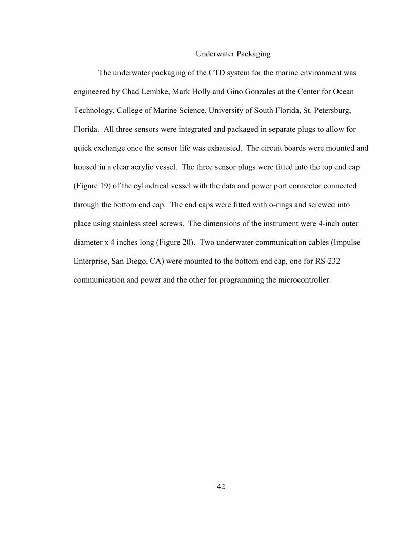
Underwater Packaging
The underwater packaging of the CTD system for the marine environment was
engineered by Chad Lembke, Mark Holly and Gino Gonzales at the Center for Ocean
Technology, College of Marine Science, University of South Florida, St. Petersburg,
Florida. All three sensors were integrated and packaged in separate plugs to allow for
quick exchange once the sensor life was exhausted. The circuit boards were mounted and
housed in a clear acrylic vessel. The three sensor plugs were fitted into the top end cap
(Figure 19) of the cylindrical vessel with the data and power port connector connected
through the bottom end cap. The end caps were fitted with o-rings and screwed into
place using stainless steel screws. The dimensions of the instrument were 4-inch outer
diameter x 4 inches long (Figure 20). Two underwater communication cables (Impulse
Enterprise, San Diego, CA) were mounted to the bottom end cap, one for RS-232
communication and power and the other for programming the microcontroller.
42

Pressure Sensor
RTD Sensor
Conductivity Cell
Figure 19. Sensor plugs mounted to end cap
43

Underwater Microcontroller circuit board
Sensor circuit board
Figure 20. Miniature CTD system prototype
44

CTD System Description
Electronics
The CTD system electronics is comprised of three individual single-sided circuit
boards that control the sensors, microprocessor and power. The sensors are controlled by
a low-power MSP430 microcontroller device. It has a 32- bit RISC processor with 64 bit
floating point calculations. It is a highly integrated microcontroller with internal
accessible flash, D/A, A/D, references, and timing capabilities. A MAX3221 low power
RS232 level converter handles communications and an ADC1241 performs a 24bit A/D
conversion with a 60Hz digital filter and self-calibration. The sensor biases are handled
by the microcontroller’s internally self-calibrated 12- bit D/A converter.
Output
The communications standard for the CTD system is configured to RS-232 with
an automatic baud rate of 115200 to 1200 and communicates directly with a computer
equipped with a serial port. The communication software used is Telnet or
Hyperterminal with the settings 115200 bits per second, 8 data bits, none parity, 1 stop
bits, and none flow control.
Logging
The CTD system has the capability of logging data internally to 12 megabytes
memory. Currently it can log 900 lines of data, where each line contains the date, time,
temperature, conductivity, pressure, and temperature within pressure sensor. The
45

date/time stamped data is logged based upon a programmable sampling rate from 1
sample every 2 seconds to once every 24 hours.
Power
Power for the CTD system can be supplied with an internal or external battery
source. The unit requires 3 mA for the RS-232, 800 µA average quiescent, 10 mA
sampling deionized water, 22 mA sampling water at 70 mS/cm at 6 to 12 volts DC
power.
Software
The CTD software is a comprehensive program, which allows the user to
communicate with the system through the serial port. The software is a menu driven
program that allows the user to set the system clock, sampling start/stop times, sensor
bias and calibration curves, memory format, sampling rate and sample mode (raw,
parametric or calibrated) (Figure 21). It also controls the downloading of logged files
and has real-time data display capabilities. The data has the option of being displayed as
raw (voltages), parametric (ohms, Siemens) or calibrated (0C, mS/cm) except for the
pressure sensor, which is always displayed as mbars along with its temperature (0C).
Salinity measurements are then independently calculated using the temperature and
conductivity data with the Practical Salinity Scale 1978 formula.
46

Figure 21. Menu format of the CTD system
47

CHAPTER IV
RESULTS AND DISCUSSION
Conductivity Cell
Calibration and Statistical Evaluation
The conductivity cell was calibrated using International Association for the
Physical Sciences of the Oceans (IAPSO) standard seawater samples (Ocean Scientific
International Limited, Hamshire, England). The conductivity calibration procedure
entailed taking consecutives measurements of the standard’s conductivity while varying
the temperature of the solution. It is known that a solution’s conductivity is a function of
temperature, and there is a mathematical expression that relates these two variables. The
conductivity cell was submersed with a platinum resistive temperature device in a beaker
of 34.995 salinity sample and heated to 32 0C using a water bath. Once the sample
stabilized at the chosen bath temperature a conductance reading (in Siemens) was taken.
Temperature readings from the sample were taken to verify actual solution temperature.
The temperature of the water bath was reduced by 2 0C increments and measurements
were acquired from 32 to 4 0C. The measurements were taken from hot temperature to
cold temperature to reduce the formation of bubbles in the standard seawater solution
(Brown et al., 1991). Five conductance measurements were recorded and averaged to
obtain a stable reading at every given temperature. The conductivity (mS/cm) of the
48

standard seawater sample (34.995) per temperature was calculated using the Electrical
Conductivity Method formula as stated in the Standard Methods for the Examination of
Water and Wastewater, 20th Edition and TK Solver 5.0 Software. The formula states:
S=a0 + a1Rt1/2 + a2Rt + a3Rt
3/2 + a4Rt2 + a5Rt
5/2 + ∆ S [4]
Where ∆ S is given by
∆ S = [t – 15/ 1 + 0.0162 (t-15)] (b0 + b1Rt1/2 + b2Rt + b3Rt
3/2 + b4Rt2 + b5Rt
5/2)
And:
a0 = 0.0080 b0 = 0.0005
a1 = -0.1692 b1 = -0.0056
a2 = 25.3851 b2 = -0.0066
a3 = 14.0941 b3 = -0.0375
a4 = -7.0261 b4 = 0.0636
a5 = 2.7081 b5 = -0.0144
Valid from S = 2 to 42, where:
R= C (Sample at t)/ C (KCl solution at t)
The conductance (Siemens) of the conductivity cell was plotted against the calculated
conductivity (mS/cm) (Figure 22). As the conductance is a linear function of the
conductivity, linear curve parameters were regressed using the method of least squares.
The regressed line, (y=1165.0615x - 4.8709) along with the coefficient of determination
(R2= 0.9997) are also placed in the graph. This equation was then entered into the CTD
49

software program to calculate the calibrated conductivity (mS/cm) data from the
measured conductance (Siemens). The calculated R2 value (0.9997) of the conductivity
cell indicated very good linear correlation (value close to 1.000). The 95% confidence
limits, (defined by α) for the estimated values of was calculated using the formula: y
2
2/1ˆ
−+±
xx
p
SSxx
nsty α [5]
Where tα/2 , a parameter obtained from the t distribution is based on (n-2) degrees of
freedom. The variable n is the number of data points, x is the sample mean, s represents
the standard deviation, and SSxx is the sum of squares. These limits, which range from
+/- 0.28 to 0.59 mS/cm, are illustrated in figure 22 as dotted lines.
50

y = 1165.0615x - 4.8709R2 = 0.9997
30
34
38
42
46
50
54
58
0.03 0.035 0.04 0.045 0.05 0.055 0.06
Siemens
mS/
cm
Figure 22. Conductivity cell calibration curve with 95% confidence limits
A regression model was used to relate the dependent variable y (conductivity) to
the independent variables x1, x2, … xk (conductance) and calculate the predicted y
intervals. The experimental evaluation was conducted exactly as stated above for the
calibration except only five data points were measured. The conductivity cell was placed
in the 34.995 salinity sample and measurements were taken at approximately 32 0C, 24
0C, 18 0C, 10 0C, and 4 0C (+/- 0.80 0C) respectively. The conductivity values were
calculated using the known standard seawater salinity and the known temperatures. This
test was repeated on four separate occasions. The residuals for all data points were
calculated and plotted using statistical equations in Excel (Figure 23).
51

-1.5
-1
-0.5
0
0.5
1
1.5
0.03 0.035 0.04 0.045 0.05 0.055 0.06
Siemens
Res
idua
ls [m
S/cm
]
Figure 23. Residual plot for conductivity curve and repeated runs
The residual data shows that the experimental error is not random, but depends on the
conductivity measured. As the conductivity increases, so does the experimental error.
Due to this fact, the standard deviations of the residuals of each repeated conductivity
measurement were calculated separately. The conductance (x) and conductivity (y)
values for all runs were averaged and the standard deviation of the residuals calculated.
Table 3 shows the statistics data for the repeated conductivity cell measurements along
with the 2s values for the respective y-values.
52

Table 3. Average values of Conductivity and Conductance with Standard Deviation
Average Conductivity (y)
Average Conductance (x)
Standard Deviation (s)
2s
32.0967 0.03184 0.2603 0.5206
38.1437 0.03715 0.2900 0.5780
46.1776 0.0444 0.5652 1.1304
52.0576 0.0496 0.6248 1.2500
59.8116 0.05612 0.9071 1.8141
In figure 24 all data points from the five runs (calibration and repeated runs) including
the five averaged values are plotted along with the y-error bars associated with those
respective points. The y-error bars range from +/- 0.5206 to 1.8141 mS/cm.
53
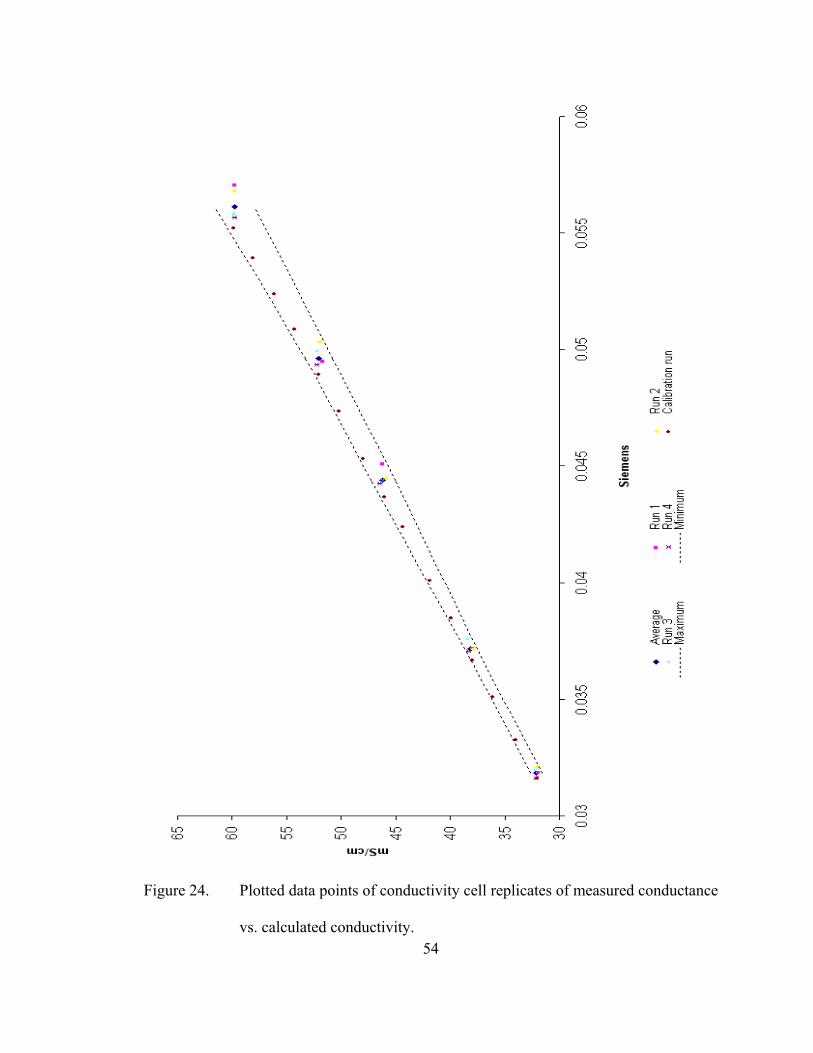
Figure 24. Plotted data points of conductivity cell replicates of measured conductance
vs. calculated conductivity. 54

Comparison Test
Once the conductivity cell was calibrated and the sample regression equation was
entered into the CTD software program, the cell was tested against a standard laboratory
conductivity probe (Mettler Toledo Inlab 730). The Mettler Toledo conductivity probe
was calibrated using a standard of 12.88 mS/cm. Conductivity standards (KCl) from
Exaxol Chemical Corp. (Clearwater, Florida) were used to perform the test. The
standards used were 2000, 5000, 7000, 10000, 12880, 15000, 20000, 30000, 40000,
50000, 60000 and 70000 µMHOS @ 25 0C. The Mettler Toledo conductivity probe is
equipped with a temperature sensor, which automatically calculates the temperature
compensation for the conductivity measurement. Temperature measurements for each
standard were recorded. The conductivity measurement taken from the fabricated cell
was corrected using the temperature compensation formula:
R/1+ 0.019 (T- 25) [6]
Where:
R= measured mS/cm reading
T= measured temperature
The temperature compensated conductivity values were then plotted against the Mettler
Toledo measurements and the sample regression equation and R2 were calculated (Figure
25). The slope of the best-fit regression line indicates a 3% deviation of the straight line.
Figure 26 shows an adequate correlation of the two sensors up to 50 mS/cm. The
differences calculated between the conductivity cell and the commercial probe were
55

approximately 3% for each conductivity value and are illustrated in figure 27. The
differences show that even though the fabricated sensor performance is a function of the
measured range, it performs relatively well until the upper limit (70 mS/cm) was reached.
y = 1.0348x - 0.2340R2 = 0.9987
0
10
20
30
40
50
60
70
80
0 10 20 30 40 50 60 7
Mettler Toledo Conductivity Probe [mS/cm]
USF
Con
duct
ivity
Cel
l [m
S/cm
]
0
Figure 25. Mettler Toledo conductivity probe vs. fabricated conductivity cell
56

0
10000
20000
30000
40000
50000
60000
70000
80000
0 20 40 60 8
[mS/cm]
uMH
OS
@ 2
5 0 C
0
USFMettler Toledo
Figure 26. Measured conductivity for conductivity cell vs. Mettler Toledo
probe
-1
0
1
2
3
4
5
6
0 20000 40000 60000 80000
Standards uMHOS @ 25 0C
Diff
eren
ce in
mS/
cm
Figure 27. Difference calculated between commercial probe and conductivity cell
57

Resistive Temperature Device
Calibration and Statistical Evaluation
The resistive temperature devices were calibrated using DI water in a temperature
controlled water bath. The sensor was submersed in a 200 ml beaker along with a
calibrated platinum resistive temperature device. Once the DI water stabilized at the
desired water bath temperature, the resistance (ohms) measurement along with the
temperature measurement from a calibrated platinum RTD was recorded. Five resistance
measurements were averaged to obtain a stable reading at each temperature. The
resistance (ohms) of the temperature sensor was plotted against the temperature (0C)
(Figure 28). A linear regression line was plotted through the known x and y-values and
the sample regression equation (y = 3.3904x – 251.6038) along with the coefficient of
determination (R2= 0.9998) that was also calculated. This equation was then entered into
the CTD software program to calculate the calibrated temperature (0C) data from the
measured resistance (ohms). Again, the calculated R2 –value (0.9998) indicates good
linear correlation between the measured (resistance) and predicted variable (temperature)
(values close to 1.000). The 95% confidence limits were calculated using formula [5]
and had a range of +/- 0.141 to 0.586 0C. Figure 28 illustrates these limits with dotted
lines.
58

y = 3.3904x - 251.6038R2 = 0.9998
0
10
20
30
40
50
60
75 80 85 90 95
OHMS
0 C
Figure 28. Resistive temperature device calibration curve with 95% confidence limits
Once the RTD was calibrated, additional runs were performed to calculate the y
prediction interval. The tests were conducted exactly as stated above for the calibration
curve, except five data points were measured. Resistance (ohms) data were collected for
five different temperatures including 50 0C, 35 0C, 25 0C, 10 0C, 5 0C. This test was
conducted on four separate occasions and plotted along with the calibration curve in an
Excel worksheet (Figure29). The residuals from the straight-line calibration data were
calculated and plotted (Figure 30).
59

74
76
78
80
82
84
86
88
90
0 10 20 30 40 50 6
Temperature 0C
OH
MS
0
CalibrationRun 1Run 2Run 3Run 4Linear (Calibration)
Figure 29. Temperature calibration curve and 4 additional runs
-1
-0.5
0
0.5
1
75 80 85 90
OHMS
Res
idua
ls [0 C
]
Figure 30. Residual plot of temperature data set
60

The residual data show that the experimental error is randomly distributed along the
sensors tested range. This implies that a constant error exists for the sensors response in
the entire data range tested. Therefore the y prediction interval can be calculated using
the formula:
2
2/11ˆ
−++±
xx
p
SSxx
nsty α [7]
Where tα/2 is based on (n-2) degrees of freedom. The variable definitions correspond to
those specified in equation 5. The prediction limits for some value of y was illustrated in
figure 31(shown as dotted lines). These limits range from +/- 0.778 to 0.964 0C.
y = 3.3904x - 251.6R2 = 0.9998
0
10
20
30
40
50
60
75 77 79 81 83 85 87 89 91
OHMS
Cel
sius
Figure 31. 95% Prediction Intervals
61

Comparison Test
Once the RTD was calibrated and the sample regression equation was entered, the
sensor was tested against a standard laboratory temperature probe (Fluke 80T-1500).
Both probes were submersed in a beaker of deionized water and heated to a specific
temperature using a recirculating water bath. The temperature devices were measured
from 50 0C to 10 0C in increments of 5 0C. The data were plotted and the sample
regression and R2 values were calculated using Excel (Figure 32). The R2 - value
(0.9997) shows good linear correlation between the novel RTD and the commercial
temperature probe. The regression coefficient or slope (0.9917) of the compared sensors
was close to 1.00. Figure 33 is the temperature comparison data of both sensors plotted
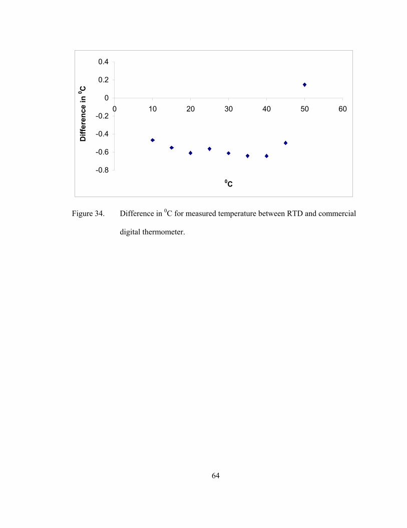
against the known temperature of the water bath. The differences between the RTD and
the commercial probe range from –0.64 to 0.15 0C and are illustrated in figure 34.
62

y = 0.9917x + 0.7388R2 = 0.9997
0
10
20
30
40
50
60
0 10 20 30 40 50 6
Digital Thermometer [0C]
RTD
[0 C]
0
Figure 32. Commercial digital thermometer vs. RTD
0
10
20
30
40
50
60
0 10 20 30 40 50 6
Temperature of Probes [0C]
Tem
pera
ture
0 C
0
RTDDigital Thermometer
Figure 33. RTD and commercial digital thermometer data plotted against calibrated
thermometer.
63
-0.8
-0.6
-0.4
-0.2
0
0.2
0.4
0 10 20 30 40 50 6
0C
Diff
eren
ce in
0 C
0
Figure 34. Difference in 0C for measured temperature between RTD and commercial
digital thermometer.
64

Depth Sensor
Comparison Test
The Intersema MS5535A pressure module (140 dbar) was tested and compared to
another discrete pressure sensor (Keller PA-10, Applied Microsystems, Sidney, BC), in
order to insure the appropriate results were obtained from the integration of the pressure
module to the sensor circuit board. The Keller PA-10 was a semiconductor bridge strain
gauge with a maximum range of 500 dbar. Both sensors were mounted into a pressure
vessel and then the vessel was pressurized and depressurized several times. Pressure
measurements were recorded for both sensors simultaneously and graphed (Figure 35).
The data were plotted and the sample regression and R2 values were calculated using
Excel (Figure 36). The R2 - value (0.9999) shows good linear correlation between the
Intersema pressure module and the Keller pressure sensor.
65

02468
1012141618202224262830323436
1 2 3 4 5 6 7 8 9 10 11 12 13 14 15 16Sample Number
Dec
ibar
IntersemaKeller
Figure 35. Comparison graph of Intersema vs. Keller pressure sensors
y = 0.9967x + 0.0249R2 = 0.9999
0
5
10
15
20
25
30
35
0 5 10 15 20 25 30 35
Keller [dbar]
Inte
rsem
a [d
bar]
Figure 36. Keller pressure sensor vs. Intersema pressure sensor
66

System Evaluation
Once the calibration of the conductivity and temperature sensors was conducted,
the complete system was evaluated both in laboratory conditions and in the field. The
CTD was placed in a bucket in the laboratory containing a known KCL standard sample
of 40000 µMHOS @ 25 0C. The CTD was programmed to take three conductivity and
temperature measurements every minute for a 24-hour period. The data were logged
internally as well as displayed real-time using RS-232 communication via hyperterminal.
The data were plotted in Excel (Figure 37).
The evaluation data revealed a small percentage of points (0.532%) that exhibit
extremely high spikes in the conductivity measurements of the known sample. These
spikes were caused by the charging of the capacitor by the super diode circuit (Ivanov,
private communication, 2005). To conserve energy in the system a reset circuit was
incorporated, which drains the holding capacitor. The super diode circuit tries to
compensate with more voltage to the capacitor. If the sample is taken when the signal is
at the top of the sign wave, the reset circuit releases and causes the super diode to over
charge the capacitor. This condition can be fixed by the addition of a capacitor to the
reset circuit. Since these spikes can be explained due to an underdamped electrical
response, the data were plotted without these data points (Figure 38). The graphed data
shows temperature and conductivity changes due to the ambient temperature of the
laboratory within the 24-hour period. The conductivity data in figure 38 were not
temperature compensated, although when the temperature compensation equation was
applied, the average measurement was 38.40466 mS/cm @ 25 0C, which is consistent
with the known KCL standard sample of 40000 µMHOS @ 25 0C. Although the system
67

did exhibit some drift within the temperature compensated conductivity measurement
with a range of 39.34095 to 37.17808 mS/cm. This 2.16287 mS/cm drift is equivelent to
a 1.523 drift in salinity @ 25 0C (Figure 39).
68

Figure 37. CTD system evaluation plot
69

Figure 38. Twenty-four hour evaluation CTD test with measured conductivity,
temperature and depth.
70

Figure 39. Salinity values for given mS/cm and temperatures.
71

Field Test
Once the CTD system was packaged in the waterproof housing and the sensors
were calibrated, it was placed in a flow-through tank. The tank was situated on a dock
within Bayboro Harbor (St. Petersburg, FL) where continuous natural seawater was
pumped into and out of the tank. The CTD system was programmed to acquire
conductivity, temperature and depth data for a seven-day period. A series of three
measurements were taken every thirty minutes and logged internally. The power source
for the CTD system was an internal 9-volt battery. After the seven-day period the CTD
system was removed from the tank and the data were downloaded and plotted (Figure
40). Also plotted on the chart were the temperature measurements for the Intersema
thermometer incorporated within the pressure module and the water level (tide) data.
This data was collected by NOS and stored in the CO-OPS database and was retrieved
from the website:
http://140.90.121.76/data_retrieve.shtml?input_code=011011111pwl&station=8726520+
St.+Petersburg,+FL
Rainfall data were also acquired for the deployment location (Albert Whitted Airport, St.
Petersburg, FL) and period (August 17th to 24th, 2005) from NOAA. A substantial
rainfall event occured on August 23, 2005 between 1900 and 2000 hours. This event was
captured by the CTD system, which measured a noticeable change in the conductivity
and temperature of the seawater.
The graphed data demonstrate the fluctuations of conductivity, temperature and
depth vs. time for the period of one week. The resistive temperature device was observed
to be consistent with the commercially manufactured sensor (Intersema). The
72

temperature data showed elevated temperatures during the day and lower temperature
during the night hours. The conductivity measurements fluctuated with temperature, but
once the parameters were incorporated into the salinity equation and the temperature was
compensated, the data was normalized. Bayboro Harbor has a mixed tidal pattern, where
successive high tides or low tides are of significantly different heights through the cycle,
which causes fluctuations in the salinity (Garrison, 1998). These fluctuations were
measured with the CTD system and were calculated using the Practical Salinity Scale
1978 [4] and plotted against time in figure 40.
73

Figure 40. Field test data of the CTD measurements with water level
74
CHAPTER V
CONCLUSIONS
Summary
The goal of this work was to develop a miniature, low cost CTD system using
novel PCB MEMS fabrication techniques combined with liquid crystal polymer (LCP)
material that measures salinity in natural waters. Two milestones had to be achieved to
reach this goal. First, the construction of LCP-based conductivity and temperature
sensors using novel PCB MEMS fabrication techniques without an expensive cleanroom
environment, and second, miniaturization of the sensors. In this work several tasks were
accomplished:
Design and construction of LCP-based conductivity and temperature sensors
using PCB MEMS fabrication techniques
Calibration and statistical evaluation of the conductivity cell and RTD
Integration of conductivity, temperature and depth sensors to make a CTD system
Packaging of the CTD system for the underwater marine environment
Seven-day field evaluation of the CTD system
75

Conventional PCB MEMS fabrication processes, such as etching and
metallization, have been coupled with a novel photolithographic process and applied on
LCP. LCP has a unique combination of physical, electrical, chemical and mechanical
properties, which makes it a good substrate for sensor applications (Wang et al., 2003).
The experiments performed have demonstrated a prototype of a novel PCB
MEMS-based CTD system capable of monitoring conductivity, temperature and depth in
natural waters. The research presented includes the design and integration of the sensors
as well as the interfacing and packaging of the system for the underwater environment. It
also includes the calibration and statistical evaluation of the conductivity and temperature
sensors. The calculated R2 values (0.9997 and 0.9998) of the conductivity cell and RTD
(respectively) indicated very good linear correlation (values close to 1.000). While the
95%prediction intervals ranged from +/- 0.5206 to 1.8141 mS/cm and +/- 0.778 to 0.964
0C.
The field evaluation test verified that all measurement principles essentially
worked as intended, and salinity data was acquired for a seven-day period. This work
demonstrates that microsensors for a CTD system can be fabricated using novel low cost
PCB MEMS processing techniques combined with liquid crystal polymer material.
76

Future Research
The next steps in the development of the PCB MEMS-based CTD system should
be the further miniaturization of the entire instrument. This can be accomplished by
redesigning the three circuit boards that control the sensors, microcontroller and power.
The initial boards were designed as separate single-sided boards to quickly troubleshoot
electrical problems. These boards can be redesigned as one thin-film multi-layer board,
thus miniaturizing the electronics of the system. Also the boards could be fabricated
using novel photolithography techniques, which have the capability to fabricate circuit
boards with smaller traces than commercial printed circuit board manufacturers. A
redesign on the system packaging could also contribute to further minimize the size of
sensing device. Most conventional packaging approaches are space inefficient and dwarf
the physical size of the system (Lyke, 1995). Several packaging alternatives need to be
investigated to protect the system for the underwater environment, such as injection
molding and waterproof coatings (Xu, 2002).
Another important issue that would require more development is expendable or
disposable sensors for the system. This type of sensors would enable the system to be
very flexible in its applications. Sensors that are pre-calibrated and then easily
exchanged with old or fouled ones allows for expanded field time for the system. This is
especially an issue with the conductivity sensor where biofouling and recalibration are
important factors that limit its ability to perform correctly. Large arrays of low-cost
disposable systems can be distributed to acquire more data, especially if these sensors are
small enough to be attached to living marine organisms.
77

REFERENCES CITED
Boehlert, G.W., Costa, D. P., Crocker, D. E., Green, P., O’Brian, T., Levitus, S., Le Boeuf, B.J., 2001. Autonomous pinniped environmental samplers: Using
instrumented animals as oceanographic data collectors. Journal of Atmospheric and Oceanic Technology, v. 18, p. 1882-1893.
Brown, N., 1991. The history of salinometers and CTD sensor systems. Oceanus, v. 34,
no. 1, p. 61-66. Brown, N., 1994. A high performance micro-power CTD sensor. Oceans conference rec IEEE, v.1, p. I-385-390. Clescerl, L., Greenberg, A., Eaton A., 1998. Standard Method for the Examination of Water and Wastewater, American Public Health Association, 20th
Edition, p. 2-44 to 2-50. Culbertson, E., 1995. A new laminate material for high performance PCBs: Lliquid crystal polymer copper clad films. 45th Electronic Components and Technology Conference, p. 520-523. Downing, J., McCoy, K., DeRoos, B., 1992. Autonomous expendable CTD profiler. Sea Technology, September, p. 49-55. Farland, R. 1975. Salinity intercomparision report, the oceanographic subprogramme for
the GARP atlantic tropical experiment (GATE). National Oceanographic Instrument Center, Washington, DC.
Farrugia, G.J., Fraser, A.B., 1984. Miniature towed oceanographic conductivity
apparatus. Oceans 1984 Conference Record, Washington D.C., September. Fougere, A., 2000. New non-external field inductive conductivity sensor (NXIC) for long term deployments in biologically active regions. Oceans 2000 MTS/IEEE conference, v.1, p. 623-630. Freeland, H., Denman, k., Wong, C., Whitney, F., Jacques, R., 1997. Evidence of change
in the winter mixed layer in the northeast pacific ocean. Deep-Sea Research, v. I 44, p. 2117-2129.
78

Fries,D., Steimle, G., Broadbent, H., Ivanov, S., Natarajan, S., Cardenas, A., Janowiak, M., Weller, T., Benson, R., Fu, J., 2002. Maskless lithographic PCB/Laminate MEMS for marine sensing systems. 35th International Symposium on Microelectronics. International microelectronics and Packaging society. IMAPS 2002 Conference, September 4-6.
Garrison, T., 1998. Oceanography: an invitation to marine science, 3rd Edition.
Wadsworth Publishing Co., CA., p. 268-269. Gileadi, E., Kirowa-Eisner, E., Penciner, J., 1975. Interfacial Electrochemistry: An Experimental Approach. Addison-Wesley Publishing Company, p. 216-218. Heckel, P.H., 1974. Carbonate buildups in the geologic record: A review. In L.F. Laporte (ed.) Reefs in Time and Space, p. 90-154. SEPM Spec. Pub. 18. Society Of Economic Paleontologists and Mineralogists, Tulsa, OK. Hooker, S.K., Boyd, I.L., 2003. Salinity sensors on seals: Use of marine predators to carry CTD data loggers. Deep-Sea Research I, v. 50, p. 927-939. Jacobs, P., Suls, J., Sansen, W., 1990. A Planar conductometric sensor showing
excellent polarization impedance characteristics. Annual International Conference of the IEEE Engineering in Medicine and Biology Society, v. 12, n. 4, p. 1484-1485.
Jayaraj, K., Farrell, B., 1998. Liquid crystal polymers and their role in electronic
packaging. Advancing Microelectronics, v. 25, p. 15-18. Kinne, O. 1964. The Effects of temperature and salinity on marine and brackish water animals. Oceanography and Marine Biology Annual Review, v. 2, p. 281-339. Kovacs, G., 1998. Micromachined Transducers Sourcebook. WCB/McGraw-Hill, NY. Lewis, E., 1980. The practical salinity scale 1978 and its antecedents. IEEE Journal of Oceanic Engineering, v. OE-5, n. 1, p. 3-8. Lykes, J., 1995. Packaging technologies for space-based Microsystems and their elements. Microenginnering Technologies for Space Systems, p.131-180. Madou, M.J., 1997. Fundamentals of Microfabrication. CRC Press LLC, p. 1-50. Matthews, J., 2004. Choosing the right pressure sensor for your OEM application.
Sensors, v. 21, n. 1, p. 38-41.
79

80
Norlin, P., Ohman, O., Ekstrom, B., Forssen, L., 1998. A chemical micro analysis system for the measurement of pressure, flow rate, conductivity, UV-absorption and fluorescence. Sensors and Actuators, v. 49, p. 34-39.
Palasagaram, J.N., Ramadoss, R., 2005. MEMS capacitive pressure sensor array fabricated using printed circuit processing techniques. SPIE Proceedings, v. 5798, p. 190-197.
Pilson, M., 1998. An Introduction to the Chemistry of the Sea. Prentice-Hall, Inc, NJ. Sansen, W., Jacobs, P., Claes, A., Lambrechts, M., 1989. A planar conductometric
sensor for continuous monitoring of haemodialysis. Proc. Engineering in Medicine and Biology Society, v. 11, p. 1381-1382.
Schlesinger, M., Paunovic, M., 2000. Modern Electroplating, 4th Edition. John Wiley and Sons, Inc. Sheats, J., Smith, B., 1998. Microlithography: Science and Technology. Marcel Dekker, Inc., NY. Varney, M., 2000. Chemical Sensors in Oceanography. Taylor Francis (UK), p. 26 Wang, X., Lu, L., Liu, C., 2001. Micromachining techniques for liquid crystal
polymer. 14th IEEE International Conference on Micro Electro Mechanical Systems, MEMS 2001, p. 126-130.
Wang, X., Engel, J., Liu, C., 2003. Liquid crystal polymer (LCP) for MEMS: Process and applications. Journal of Micromechanics and Microengineering, v. 13, p. 628-633. Wells, H., 1961. The fauna of oyster beds with special reference to the salinity factor.
Ecological Monograph, v. 31, p. 239-266. Xu, Y., Jiang, F., Lin, Q., Clendenen, J., Tung, S., Tai, Y., 2002. Underwater
sheer-stress sensor. MEMS 02 15th IEEE Conference on Micro Electro Mechanical Systems, p. 340-343.