Embed Size (px)
Citation preview

DEVELOPM ENT OF A LASER SCANNING SYSTEM
FOR TIIE INSPECTION 0 F SURFACE DEFECTS
BY SIIANE BEARY (B.A., B.A.I.)
This thesis is submitted as the fulfilment of the
requirement for the award of degree of
MASTER OF ENGINEERING (M.Eng)
By Research from
DUBLIN CITY UNIVERSITY
(DCU)
N O V EM BER 1996

DECLARATION
I hereby certify that this material, which I now submit for
assessment on the programme of study leading to the award of
Master of Science in Mechanical Engineering is entirely my
own work and has not been taken from the work of others
save and to the extent that such work has been cited and
acknowledged within the text of my work
Signed Date
u

ACKNOWLEDGEMENTS
I would like to express my sincerest gratitude to my project supervisor
Dr M El-Baradie, who originally conceived the project and who guided me in a very
professional manner throughout the course of my research
A major amount of gratitude is due to all the staff of the Mechanical Workshop
These included (in no particular order) Martin Johnson, Ian Hooper, Liam Domican,
Paul Donohoe and Tommy Walsh All of these people contributed in various ways to
the success of my thesis They also contributed valuable companionship and advice
both inside and outside the workplace
I would also like to thank David Moore a postgraduate like myself with whom I had
the pleasure of sharing an office and much friendship during my two years here
Finally I would like to thank all my family for all the support they gave me during my
time at DCU-especially my mother who has always contributed invaluably to anything
I have done

Contents List. Page number
- Title
- Declaration
- Acknowledgements
- Contents
- Abstract
- List of figures
- List of tables
CHAPTER ONE
1 - Introduction 2
CHAPTER TWO
2.- Literature survey
2 1 - Lasers 5
2 2 - Properties of Lasers 5
2 2 1 - Radiance 5
2 2 2 - Directionality 7
2 2 3 - Monochromaticity 8
2 2 4 - Coherence 9
2 2 5 - Power & Energy output 10
2 3 - General Classification of Lasers 10
2 3 1 - Helium-Neon 10
2 3 2 - Molecular lasers 11
2 3 3 - Solid Stale lasers 11
2 3 4 - Semiconductor lasers 12
2 4 - Applications of lasers 12
2 4 1 - Low-power applications 13
IV

2 4 2 - High-power applications . 14
2 5 - Scanning Technology 16
2 5 1 - Mechanical Scanners 17
2 5 2 - Acousto-optic Deflectors 21
2 5 3 - Electro-optic Deflectors 23
2 6 - Surface Inspection 26
2 7 - Laser Scanning Inspection Systems 28
2 7 1 - Automatic surface inspection of continuously and batch 30
annealed cold-rolled steel strip
2 7 2 - Quality Control technology for Compact Disc 32
manufacturing
2 7 3 - Other applications of laser inspection systems 35
CHAPTER THREE
3 - Design and development of Inspection system
3 1 - Introduction 37
3 2 - Overview of the system 37
3 3 - Measuung system 40
3 3 1 - Laser sensor 41
3 3 1 1 - Triangulation Method 43
3 3 1 2 - Diffuse reflection technique 46
3 3 1 3 - Error influences 47
3 3 2 - Power supply unit 50
3 3 3 - Interface card 50
3 3 4 - Measured value output 52
3 4 - X-Y kinematics system 53
3 4 1 - Roland DXY 1300 plotter 53
3 4 2 - Automatic control of plotter 56
3 4 2 1 - Control by AutoCAD 56
3 4 2 2 - Formula for calculation of scanning parameters 58
3 4 2 3 - Control through command system 59
v

3 5 - Software
3 5 1 - Software configuration
3 5 2 - Sample measurement process
60
60
60
CHAPTER FOUR
4.- Experimental results and Discussion
4 1 - Introduction 63
4 2 - Analog results 63
4 3 - Aluminium digital tests 66
4 3 1 - Selection of initial measuring parameters 66
4 3 2 - Representation of output signal 67
4 3 3 - Coordinate system 71
4 3 4 - Experimental errors 72
4 3 5 - 3D view of plate surface 74
4 4 - Stainless Steel digital tests 77
4 5 - Brass digital tests 81
4 6 - Copper digital tests 84
4 7 - Polycaibonate digital tests - 87
4 8 - Perspex digital tests 91
4 9 - Summary of results os materials tested 92
CHAPTER FIVE
5.- Conclusions
5 1 - General conclusions 94
5 2 - System hardware development 94
5 3 - System software development 95
5 4 - Conclusions on the experimental results 97
5 5 - Recommendation for further work 98
VI

APPENDICES 104
REFERENCES 99
v u
ABSTRACT
DEVELOPMENT OF A LASER SCANNING SYSTEM FOR THE INSPECTIONOF SURFACE DEFECTS
BYSHANE BEARY
The main objective of this project is the development of a low cost laser scanning system for the detection of surface defects The inspection system is based on a laser sensor, power supply unit and an X-Y table All of these components are interfaced with a personal computer The system developed is capable of measuring surface defects within the range of greater than or equal to 1mm For the experiments carried out it was intended to assess the sensors measuring ability under certain headings The two main headings covered were accuracy and repeatability Other important subjects included examining the measuring limits of the system, examining the effect of using materials of different reflection abilities, and the possible cause of errors in the system
Vlh

LIST OF FIGURES Page number
Fig 1 Generalisation of laser scanning technology 17
Fig 2 Galvanometer mirror 18
Fig 3 Partially illuminated polygon 19
Fig 3 Partially illuminated polygon 20
Fig 5 Diagram of Acousto-optic device 22
Fig 6 Acousto-optic cell operating as a deflector 22
Fig 7 Electro-optic effect 24
Fig 8 Electro-optical prism 25
Fig 9 One-dimensional laser scanner flaw detector 28
Fig 10 Two-dimensional laser scanner flaw detector 29
Fig 11 Surface inspection system 3 1
Fig 12 Typical inspection report on monitor 32
Fig 13 Block Diagram of CD Inspection System 34
Fig 14 Photograph of the complete system in operation 38
Fig 15 Selection of Brass, Copper, Polycarbonate and Stainless Steel 38
sample plates
Fig 16 Block digram of Rig 39
Fig 17 The two options for the structure of the measuring system 40
Fig 18 Diagram of Operation of optoNCDT sensor 41
Fig 19 Block diagram of ILD 2005 sensor 42
Fig 20 Diagram of laser based optical tnangulation system 44
Fig 21 Principals of diffuse and real reflection 46
Fig 22 Angle Influences 48
Fig 23 Sensor arrangement for ground or striped surfaces 49
Fig 24 Sensor arrangment for holes and ridges 49
Fig 25 Block diagram of Power supply unit PS 2000 5 1
Fig 26 Block diagram of Interface card IFPS 2001 50
Fig 27 Two isometric views of the plotter 54
Fig 28 Some of the mam operational functions 55
Fig 29 Diagram of sample plate 56
IX

Fig 30 Plotted AutoCAD drawing 57
Fig 31 Sample aluminium plate used in analog experiments 63
Fig 32 2D Graph of Analog test results on Aluminium plate 65
Fig 33 Plotted AutoCAD drawing 66
Fig 34 2D Graph of Aluminium test results 68
Fig 35 Extract of results table in Appendix D highlighting data for smallest defect 69
Fig 36 Actual coordinates/dimensions of sample plate 71
Fig 37 Coordinates/dimensions of sample plate calculated by the sensor 72
Fig 38 Graph of results for first scan line 73
Fig 39 Graph of results for second scan line 74
Fig 40 3D Graph of Aluminium plate compared to actual sample plate 75
Fig 41 2D Graph of Stainless Steel test results 77
Fig 42 Graph of Stainless Steel results of points 1370 to 1460 and their 78
corresponding plate coordinates
Fig 43 Graph of Stainless Steel results of points 2050 to 2160 79
Fig 44 2D Graph of Brass test results 81
Fig 45 Graph of Brass results of points 1190 to 1323 and their corresponding 82
plate coordinates
Fig 46 Graph of Brass results of points 1864 to 2135 83
Fig 47 2D Gi aph of Copper test results 85
Fig 48 Graph of Copper results of points 1369 to 1469 86
Fig 49 Graph of Copper results of points 2002 to 2225 - 86
Fig 50 2D Graph of Polycarbonate test results 88
Fig 51 Graph of Polycarbonate results of points 1362 to 1476 89
Fig 52 Graph of Polycarbonate results of points 2027 to 2289 89
Fig 53 2D Graph of Perspex test results 91

LIST OF TABLES Page number
Table 1 Mam applications of lasers 16
Table 2 Specifications of the sensor 43
Table 3 Signal output of the sensor 53
Table 4 Pen speeds available using AutoCAD 59
Table 5 Analog output for aluminium plate 64
Table 6 Relationship between output and coordinate system 69
Table 7 Calculated characteristics of the Stainless Steel plate 80
Table 8 Calculated characteristics of the Brass plate 83
Table 9 Calculated characteristics of the Copper plate 87
Table 10 Calculated characteristics of the Polycarbonate plate 90
Table 11 Summary of Results 92
XI

CHAPTER ONE

CHAPTER ONE
On-line control plays an increasingly important role in modern manufacturing
processes The introduction of laser scanning control systems into the manufacturing
process allows 100% material testing and prevents defects and production
deterioration from being undetected The principals of optical inspection used by
these systems are of a non-contact nature Thus they can be applied at all the usual
temperatures, allow a high resolution (eg pinholes down to 10|im in size can be
detected), and can be easily adapted to the requirements of automated inspection of
continuously moving parts Illumination,with monochromatic laser light provides
images of better quality and allows frequency filtering which is very important when
working under normal illumination Scanning infers that one .point at a time is
illuminated from one single direction Thus in practice, an image with high contrast
and resolution can be captured
Laser scanning systems have been successfully implemented in the inspection of
widely varied material surfaces In the plastic industry for example, standardised
inspection systems now exist for transparent, coated or coloured films (photographic
films, video tapes, audio tapes, filters, protective films etc) and plates The most
commonly occurring types of faults in these materials are inclusions, holes, bubbles,
inhomogenities, surface defects (scratches, indentation, pitting) and defects in
coatings It is usually required not only to detect faults but also to classify them To
enable types of faults to be distinguished unambiguously, a catalogue of these is first
assembled for each material t/From this the optical characteristics of the individual
types of defects are determined and summarised as a defect matrix i e type of
defect/inclusion, scratches or indentation against the mode of observation
Inspection of the material immediately following its production helps to prevent
situations where unusable material is produced over a long period This thesis is
mainly concerned with how the type of surface defects encountered in the
1 - Introduction
2

manufacturing industry can be measured It outlines the experimental results of the
laser scanning system developed when using different sample materials, mainly metals
and plastics
The mam objective of this project is the development of a low cost laser scanning
system for the detection of surface defects The inspection system is based on a laser
sensor, power supply unit and an X-Y table AH of these components are interfaced
with a personal computer The system developed is capable of measuring surface
defects within the range of greater than or equal to 1mm
In this thesis the literature survey is presented m Chapter 2, which is mainly
concerned with lasers, scanning technology and laser scanning inspection systems
The configuration of the inspection system is described in Chapter 3, which includes
the laser sensor, X-Y table, the computer interfaces and the software used to control
the measurement process The principal of optical triangulation which is used as a
non contact method of determining defect measurement is also presented and
discussed A description of the software developed for the measurement process is
presented along with how the software was used in a sample measurement process
Chapter 4 outlines the experimental results which were carried out using the
developed system For these experiments six different workpiece matenals were used
These included Aluminium, Stainless Steel, Brass, Copper, Polycarbonate and
Perspex Different materials were used in order to compare the system performance
on matenals of different reflective capabilities Also in all the six workpiece matenals
defects in the form of holes varying from 8mm to 1mm wcie incorporated into
detection The different size holes were used to test the measuring limits of the laser
sensor The performance of the system with regard defect size and material reflective
properties is summarised at the end of this chapter The conclusions and
recommendations for further work are outlined in Chapter 5 These include a look at
both the systems hardware and software development as well as analysis of the
experimental results
3

CHAPTER TWO

CHAPTER TWO
2 1 - Lasers
A laser is a device which produces and amplifies light [1] The acronym LASER
stands for light Amplification by Simulated Emission of Radiation The word light
refers to ultraviolet, visible or infrared electromagnetic radiation The word radiation
refers to electromagnetic radiation of which light is a special case The key words m
the acronym are amplification by stimulated emission A laser amplifies light and it
does this by means of the phenomenon of stimulated emission Most, but not all,
lasers are also oscillators because an optical resonator is used to provide feedback and
energy storage Laser light has many advantages over an ordinary light source The
are several key properties of laser light which ensure that lasers are such useful tools
in an incredible variety of applications The primary properties of concern in
industrial applications are radiance, directionality, monochromaticity, coherence and
the various forms of output
2 2 - P toper lies o f la set s
2 2 1- Radiance
The radiance of a source of light is the power emitted per unit area of the source per
unit angle [2] The units are watts per square metre per steradian A steradian is the
unit of solid angle which is the three dimensional analogue of a conventional two-
dimensional (planar) angle expressed in radians
The term brightness is a term frequently used instead of the proper term luminance
Luminance is like radiance except that the response of the standard eye is taken into
account, and therefore only applies to visible light The units are lumens per unit area
2.- Literature survey
5

per unit solid angle A lumen is the photometric equivalent of a radiometric unit
(absolute unit of power), the watt The field o f photometry takes into account the eye
response whereas the radiometry deals with absolute physical quantities However,
the usual practice is normally to only deal in radiometric quantities
Lasers generally have an extremely high radiance output For example, a helium-
neon laser with an output of lmW will have an output spot diameter of about 1mm
and a beam divergence of about lmrad The radiance of the sun in contrast is only
1 3 * 106 W/in2/sterad even though the sun emits a power of 4 * 1026 W
Radiance is an extremely important concept High radiance obviously means that a
beam has a small divergence angle unless the power is very large Lasers achieve high
radiance at relatively low power levels The amount of power that can be
concentrated on a spot by focusing a beam of light is directly proportional to the
radiance In laser work an important concept is the inadiance (also called intensity)
Irradiance is the power per unit area falling on a surface at a given point For
convience the units are usually given as watts per square centimetre (W/cm2) For
example a HeNe laser beam could be focused by a 2 5cm focal length lens to an
irradiance of over 200W/cm2 The spot diameter of the beam would only be about
25|im High irradiances are important to such materials processing applications as
cutting, drilling and welding However, the spot size required is of the order of 0 1-
1 Omm for most applications One thousand watts focused to a 0 1mm diameter spot
produces an average irradiance of nearly 13MW/cm2 This is still very high compared
with what can be achieved with conventional methods
The high radiance of lasers' results in small spot sizes when mirrors or lens are used to
focus the beam This is what then produces the very high irradiance Therefore the
radiance of a laser is ducctly linked to the small beam divcigcncc (ducctionalily) of a
laser
1'i6

2 2 2 - Directionality
Everyone has seen the publicity spotlights at circuses and big events Their beams of
light penetrate the heavens , apparently diverging little as they disappear into the
night sky While these spotlights produce beams that don’t expand much over
hundreds of yards, a laser beam the same size would propagate hundreds of miles
without expanding much
The divergence of lasers are typically measured in milliradians This very small
divergence results from the requirement that light must make many round trips of the
laser resonator before it emerges through the partially transmitting mirror Only rays
that are closely aligned with the resonator’s centreline can make the required number
of round trips, and these aligned rays diverge only slightly when they emerge [3]
But just as it’s impossible for a laser to be perfectly monochromatic, it is impossible
for a laser to produce a nondiverging beam of light Although the divergence of a
laser beam can be very small when compared to light from other sources, there will
always be some divergence
In effect, the beam of light from a laser is a narrow cone of light that appears to be
coming from a point As such, geometry plays no role in the focusing of a laser
beam, at least not the raw beam or one that has simply been expanded or reduced in
size The limiting effect which is a basic property of light is diffraction Diffraction
causes collimated beams of light to diverge and causes bending of light beams around
sharp edges of objects It also limits the size of a focused spot A lens with an f-
number ( the ratio of the lens focal length to aperture or beam size ) of one will focus
an ideal diffraction limited laser to a spot radius approximately equal to the
wavelength of the light Clearly, a 1mm focal length lens would be impractical, but if
the beam is expanded to 1cm m diameter, then a 1cm focal length lens would be
practical and achieve the desired result Places where such small spot sizes might be
required are integrated circuit manufacturing and recording and reading of optical
data storage media such as laser video or audio discs and optical memories for
computers
7

2 2 3 - Monochromaticitv
The term monochromatic literally means single colour or single wavelength In order
to understand this concept observe the following process [4] Because a glass prism
is dispersive, it separates white light into its component colours The bandwidth of
white light is as wide as the whole visible spectrum, about 300 nanometers (nm) If
light that is nominally red falls on the prism, it is separated into its nominal
wavelengths too But, in this case the bandwidth is far less, perhaps only 10 or
20nm The prism will produce a narrower band of colours, ranging from dark red to
light red However the pnsm will not have any discernible effects on the red laser
light because its bandwidth is very small when compared with the red light from the
filter For example the bandwidth of a HeNe laser is typically less than lnm
However, no light source can be perfectly monochromatic Lasers tend to be
relatively monochromatic but this depends on the type of laser in question
Monochromatic output, or high frequency stability, is of great importance for lasers
being used on interferometnc measurements since the wavelength is a measure of
length or distance and must be known with extreme precision and it must remain
constant with time The same holds true for lasers used in chemical and many other
scientific analytical applications Precise wavelength definition is not generally
considered important in materials processing though some infrared wavelengths are
thought to work better in cutting or drilling of certain polymers, but generally in
processes controlled by thermal effects precise wavelength control is not critical
However, processing of polymeric materials with ultraviolet wavelengths, such as
are available from excimer lasers, is entirely different In this case precise tuning of
the wavelength to resonate with the molecular bond will probably significantly
enhance the efficiency of material removal Absolute monochromaticity is an
unattainable goal which we can only approach by refining our light sources
8

2 2 4 - Coherence
The easiest way to explain the concept of coherence is the marching band analogy [5]
In a parade of marching bands one would see a nearly perfect spatial coherence across
the rows and columns If we know the position of one marcher, it is probable to
know the relative position of any of the other marchers in the band An incoherent
light source on the other hand is more analogous to the people on a busy city road at
rush hour The concept of coherence is one of considerable interest in a wide variety
of laser applications such as communications, holography, doppler velocimetery and
interferrometnc measurements Lasers provide a high radiance source of light with a
high degree of coherence This combination is not available from any other source of
light
A coherent light beam will have three distinct charactenstics
1 the same wavelength
2 the same direction
3 the same phase
The wavelength is the distance between two like points on a wave The light waves in
a laser beam all have the same wavelength The phase of a wave, in its most practical
sense, refers to its position relative to another wave If two waves are in phase, they
are lined up in space and time If the waves are shifted in respect to one another, then
they are out of phase by a given amount What’s more, the light from a laser exhibits
both spatial coherence and temporal coherence Its spatial coherence means that light
at the top of the beam is coherent with the light at the bottom of the beam The
farther you can move across the beam and still find coherent light, the greater the
spatial coherence Temporal coherence, on the other hand, comes about because
two waves in a laser beam remain coherent for a long time as they move past a given
point That is, they stay in phase with each other for many wavelengths Coherence
also causes a problem called laser speckle Speckle is produced when laser light is
9

scattered from a diffusing surface Speckle can be used in some measurement
applications, but can create problems in others
All the things that can only be done using laser light can be done because laser light is
coherent Monochromatic laser light can be used to probe the structure of atoms or
to control complex chemical reactions - because it is coherent Highly directional
laser light can transport energy over large distances or focus that energy to very large
intensities - because it is coherent Phase consistent laser light can produce realistic
three-dimensional holograms or create ultra short pulses of light whose duration is
only a dozen or so optical cycles - because it is coherent The coherent light from a
laser is indeed a different breed of light from that emitted from any other source
2 2 5 - Power and Energy Output
The output of lasers may be pulsed or continuous Lasers used for alignment,
measurements and other low-power applications usually have a continuous output
whereas materials processing lasers may be either pulsed or continuous Some lasers
are capable of both pulsed and continuous operation
2 3 - General Classification of Lasers
There are many different types of laser available for industrial use at the moment The
application of each type is dependent on its particular characteristics A brief
description of the main lasers in use today and their unique properties [6],[7],[8] is
given below
2 3 1 -Helium-neon lasers (HeNe^
• Electrically pumped gas laser
• Bright red beam at 632 8nm and also infrared lines at 1 15 and 3 39|im
• Electrical efficiency typically - 0 1%
10

• Energy is transferred from electrons to the HeNe atoms leaving them m an excited
state
• Output power varies from a fraction of a mW up to 50mW
• Operating life - 15,000 to 20,000 hours
• Most common failure mechanism is cathode decay
• Commonly used in supermarket checkout stands, home videodisk players and
laser pnnters
2 3 2 - Molecular lasers
• Operate on the rotational, vibrational and electronic energy levels of molecules
• Most important of these is C02 laser which is based on vibration technique
• Capable of generating very high average powers with relatively high electrical
efficiency
• Commercial C 02 lasers with average power greater than 20kW are available, and
kilowatt C02 lasers are common
• Their electrical efficiency can exceed 10%
• Commonly used for applications such as cutting, welding, and heat treating
materials
• C02 lasers are also important in medical and research applications
• A newer type of molecular laser, the excimer laser, is important because it is a
good source of ultraviolet light
2 3 3 “ Solid-state lasers
• Lasing atoms are embedded in a solid piece of transparent matenal called the host
• Most common examples are Nd YAG lasers, Nd glass lasers, and Cr ruby
• Optical pumping provides the energy to create a population inversion
• Usually water cooled
• Largest application of solid-state lasers is in tactical military equipment, where
they are used in rangefinders and target designators
11

• Also used in materials processing, medicine and scientific research
2 3 4 - Semiconductor diode lasers
• A laser diode is a junction between p-doped and n-doped materials
• The resonator is often formed by polishing the end faces of the semiconductor
• Stimulated emission occurs before an atom has time to lose its energy another way
• Most common type is the GaAs laser
• Wavelength range from 0 33|im UV - 40|im IR
• Outputs in the milliwatt range
• Diode lasers are the most ubiquitous lasers in existence
• They are small, rugged and cheap but not powerful yet
• They will probably replace gaseous and optically pumped lasers in a number of
applications in the near future
2 4 - Applications o f Lasers
Like the laser itself, the applications of lasers involve a wide range of fields The
unique characteristics of laser light are what make lasers so special The capability to
produce a narrow beam doesn’t sound very exciting, but it is the critical factor in
most laser applications Because a laser beam is so narrow, it can read the minute,
encoded information on a stereo CD - or on the bar-code patterns in a grocery store
Because a laser beam is so narrow, the comparatively modest power of a 200 watt
carbon-dioxide laser can be focused to an intensity that can cut or weld metal
Because a laser beam is so narrow, it can create tiny precise patterns in a laser
printer Generally speaking the applications of lasers can be broken down into two
separate categories Low-power applications and High-power applications
12

2 4 1- Low-powcr Applications
When we talk about low power lasers we generally mean in the l-50mW range,
usually HeNe or diode lasers The main applications of such a laser are alignment,
gauging, inspection, interferometery and holography [9] The characteristics of
lasers which make them useful in these type of applications are high
monochromaticity, coherence and high radiance
Interferometric applications such as holography, speckle, measurements and Doppler
velocimetry require good spatial and temporal coherence, as well as varying levels of
frequency stability and good mode quality Laser interferometery is used to make
measurements or to control machines and motion systems to within a fraction of a
millimetre The small beam divergence of lasers gives them the unique capabilities in
alignment applications whether for machine set up or building construction The high
radiance permits the use of lasers for accurate triangulation measurements and control
of machines such as robots
Laser printers are capable of producing high quality output at very high speeds Until
several years ago they were also very expensive, but since printers based on
inexpensive diode lasers were introduced, the cost dropped dramatically In a laser
printer, the laser writes on an electrostatic surface which in turn transfers ink to the
paper Low-power lasers have other applications in graphics as well Laser
typesetters write directly on light-sensitive paper, producing camera ready copy for
the publishing industry Laser colour separators analyse a colour photograph and
create the information a printer needs to print the photograph with four colours of
ink Laser platemakers produce the printing plates so that newspapers can be printed
in locations far from their editorial offices Also, laser bar-code scanners are used for
the chcckouts in a supcrmaikct The nariow beam o f the IIcNc laser in Ihcsc
machines scans the bar-code pattern, automatically reading it into the store’s
computer
13

There seems to be no end to the ingenious ways a narrow beam of light can be put to
use In sawmills, lasers are used to align logs relative to the saw The laser projects
a visible stripe onto the log to show where the saw will cut it as the sawman moves
the log into the correct position On construction projects the narrow beam from a
HeNe laser guides heavy earth-moving equipment Laser light shows herald the
introduction of new car models and rock concerts Diode lasers are the light sources
in many fibreoptic communication systems Laser gyroscopes guide the newest
generation of commercial aircraft’s Finally, low-power lasers are widely used in
industry for automatic on-line inspection processes, and this is the main area which
this project is concerned with These type of applications would not be feasible using
conventional light sources
2 4 2 - High-power Applications
The main application of high-power lasers is in materials processing, where lasers are
used to cut, drill, weld, heat-treat, and otherwise alter both metals and non-metals
[10] Lasers can drill tiny holes in turbine blades more quickly and less expensively
than mechanical drills Lasers have several advantages over conventional techniques
of cutting materials For one thing, unlike saw blades or knife blades, lasers never
get dull For another, lasers make cuts with better edge quality than most mechanical
cutters The edges of metal parts cut by laser rarely need to be polished or filed
because the laser makes such a clean cut to start with The major drawback to laser
cutting is thickness of the material to be cut Nd-YAG lasers can cut up to about
5mm thickness and C 02 lasers can cut up to about 20mm at reasonable speeds Large
amounts of assist gas are required If oxygen is used, the operating cost can be quite
high However, if air can be used , this cost is virtually eliminated
Most of the statements concerning cutting apply to hole pieicmg with solid state
lasers Added to the list should be the fact that holes can be dulled at large angles to
the surface Hole depth-to-diameter ratios of 20 1 are common High repeatability
and accurate placement are achievable The major drawback to laser hole piercing is
14

that the holes arc tapered and some recast material is usually present in the entrance
side, and dross due to oxidation may stick to the exit hole.
Laser welding can often be more precise and less expensive than conventional welding
techniques. Moreover, laser welding is more compatible with robotics, and several
large machine-tool builders offer fully automated laser-welding systems to
manufacturers. There are limitations to laser welding, as with any process. Spot
welding with pulsed solid state lasers is limited to about l-2mm penetration, and
continuous seam welding with multikilowatt C 02 lasers is limited to around 1cm
penetration. High carbon steels and certain other alloys are difficult to weld without
cracking because of the rapid heating and cooling involved. Reasonably good fitup
between parts is required for successful laser welding.
Laser heat-treating involves heating a metal part with laser light, increasing its
temperature to the point where its crystal structure changes. It is often possible to
harden the surface in this manner, making it more resistant to wear. Heat-treating
techniques require some of the most powerful industrial lasers there are, and it is one
application where the raw power of the laser is more important than the narrow beam.
Although heat-treating is not a wide application of lasers now, it is one which is likely
to expand significantly in the coming years.
Lasers started out in research laboratories, and many of the most sophisticated ones
are still there. Chemists, biologists, spectroscopists, and other scientists count
lasers among the most powerful investigation tools of modern science. Again, the
lasers narrow beam is valuable, but in the laboratory the other characteristics o f laser
light are often important too. Because a laser beam contains light o f such pure
colour, it can probe the dynamics of a chemical reaction while it happens or it can
even stimulate a reaction to happen.
In medicine, the lasers narrow beam has proven a powerful tool for therapy. In
particular, the carbon dioxide laser has been widely adopted by surgeons as a
bloodless scalpel because the beam cauterises an incision even as it is made. Indeed,
15

some surgeries which cause profuse bleeding had been impossible to perform before
the laser The laser is especially useful on ophthalmic surgery because the beam can
pass through the pupil of the eye and weld, cut or cauterise tissue inside the eye
Before lasers, any procedure inside the eye necessitated cutting the eyeball open
In summary Table 1 below gives an idea of the main areas of concern for low and
high-power applications Having given a brief insight into these areas I intend now to
concentrate on the applications of low-power lasers, specifically the use of lasers as
an inspection tool which is the main area of concern of this project
Low-Power laser applications High-Power laser applications
Alignment
Gauging
Inspection
lnterferometery
Holography
Surface Hardening
Welding
Cutting
Laser Marking
Hole Piercing
Alloying and Cladding
Table 1 Mam applications of lasers
2 5 - Scanning rechnolozv
Besides the laser itself, most laser applications require other components and devices
These components can be divided into the broad categories of modulators and
scanners, detectors, positioning systems and imaging optics This section deals with
scanning devices which operate on the laser beam to change its direction Scanners
are used outside the cavity to direct the beam toward a specific location There are at
present three main types of beam deflection They are mechanical, acousto-optic and
electro-optic
16

Another method of differentiating between major scanning techniques is shown in Fig
1 This method divides scanning technology into two classes high inertia and low
inertia This identifies the operational distinction between massive and agile control
capability [11]
Rotational-Mechanical Vibrational-Mechanical
Mirror & Prism Techniques Non-Mechanical Tech
Fig 1 Generalisation of laser scanning technology [11]
2 5 1- Mechanical scanners
Most laser scanners today use mechanical rotation [12] The inertia of high speed
rotation gives a very stable scan rate, and fine tuning by electronics can increase
stability to about one part in 30,000 Depending on the ratio of the facet width to the
beam size at the facet, the active writing time can be 95% of the total operating time
Mechanical scanners employ the actual physical movement of a mirror, prism or
similar components to alter the direction of the laser beam [13] The component is
generally moved using an electric motor or through a galvanometer/coil arrangement
The prime constraint upon this technology is that it requires a relatively rigid scan
format, limited by the intrinsic high inertia of the mechanical system Other
constraints upon rotational-mechanical scanners are the systems parameters which
may inhibit the use of rotating components and their associated bearings, motor drive
and control systems Generally mechanical scanners tend to be slow and
17

difficult to control precisely, but they offer the advantage of relatively low price,
durability and simplicity
Galvanometei m inor
The galvanometei mmoi woiks on the same punciple as the d’Arsonval movement
in an analog meter [14] A coil of wne mounted between the poles of a permanent
magnet will rotate if a current is passed thiough it Since the current causes a
magnetic field around the coil, the magnetic field of the permanent magnet will repel
the coil and cause it to move Varying the amount and direction of current in the coil
will cause it to move different amounts in different directions A mirror mounted on
the coil will move with it and can be used to reflect a laser beam in different
directions
Galvanometer mirrors offer the advantage of a large angle of deflection and little or
no distortion of the laser beam They are available in several different speeds and
resolutions However, they are limited by different parameters [15] A large scan
angle and/or a reasonable beam diameter causes slow scan rates (some few hundreds
Hz) A high scan rate (up to 20kHz) causes small mirror sizes and only sinusoidal
motion functions An advantage is that the centre of deflection coincides with the
mirror axis This fact simplifies the optical corrections Fig 2 shows a common
galvanometer mirror A combination of two such mirrors at right angles to each
other can be used to position and scan the laser beam in two directions
Coil-mounted mirror
Fig 2 Galvanometer mirror [14]
18

Rotating mirror
One of the earliest and most familiar lotating mmoi techniques is illustrated in Fig 3
[16] A multifaceted polygon is illuminated with a single nanow beam such that
only a fraction of the mnroi subtense is exposed to the beam at any time An angulat
displacement of the polygon through the angle 9 impaits a 29 angulai displacement
to the reflected beam This double speed scan continues until the corner of the
polygon encounters the illuminating beam, wheieupon the reflected beam is split in
two one part finishing the scan and the balance initiating the new scan Howevei,
this system is optically and mechanically inefficient since only a small fraction of the
mirrored surface is actively engaged in reflecting the illuminating beam
Rotating prism
A penta-prism can be used to turn a laser beam through a right angle even though the
prism is not precisely aligned [17] By rotating the prism about the axis of the
incident beam, as illustrated in Fig 4 , the output beam sweeps out a flat plane
Systems of this type are used on construction sites to align ceilings, walls and
foundations In many cases a HeNe laser is used, so that the scanning laser beam
produces a red line on the object which can be viewed by the human observer in
RETRACE INTERVAL = Transit Time AcrossIlluminating Beam
ILLUMINATINGBEAM
Fig 3 Partially illuminated polygon [16]
19

order to align the object If greater accuracy is required, or automated alignment
desirable, a position detector can be used By using a laser beam which scans out a
horizontal plane, an automated position detector system can be used to detect the
beam and conti ol the blade on the earth moving equipment, so that an absolutely flat
suiface can be graded Faimeis and load buildeis use these systems to grade then
fields
Fig 4 Penta-prism scanner [17]
Properties o f Mechanical scanners
There are of course limitations to using mechanical deflectors which are summarised
in the following points [18],[19]
• Scan speed - ms rates
• Complex design - expensive
• Susceptible to damage
• Limited life due to mechanically moving parts
• Suffers from ’wobble (facet to facet pyramidal error)
Applications o f Mechanical Scanners
Mechanical scanners are used when a large range of movement is needed and high
speed is not necessary [20] A common application of a scanner such as a
20

galvanometer mirror is for a laser light show Laser light shows use the special
properties of the laser beam to create visual displays on a large scale The scanner is
used to trace a pattern with the beam from a visible laser light on some surface like a
screen or a wall By scanning rapidly enough, the traced pattern appears to be one
solid line Effects can be enhanced by adding smoke or steam in the beam path so that
it too can be seen Many commercial companies offer laser light shows for concerts
and as stand-alone events There are several permanent light show displays in the
country
Scanning the beam of a high power laser on a surface can be used to engrave patterns
on that surface When the engraving only requires medium resolution on a small
scale, a mechanical scanner can be used to position the beam The scanner is often
controlled by interfacing it with a computer that provides the appropriate current for
each scanning position and allows the user to program individual position values or a
model of the image to be engraved
2 5 2 - Acousto-optic Deflectors
Many of the applications that employ lasers require the laser to be modulated and
deflected Acousto-optic devices are perhaps the most versatile means of
incorporating information onto a laser beam In order to understand acousto-optic
deflectors we must first discuss modulators Acousto-optic modulators are used for
the production of short, high-power pulses from lasers, beam deflection, amplitude
modulation and frequency modulation [21] An acousto-optic modulator is a device
that uses a transparent solid block of material, such as fused quartz, to which is
attached a piezoelectric transducer The acousto-optic effect is caused by sound
waves in the crystal If pressure is applied to the material it causes a change in the
materials refractive index If the applied pressure is varied sinusoidally, the changes
in the refractive index will vary as well In an acousto-optic device (Fig 5 ), high
frequency pressure changes are created in a crystal by vibrating its surface with a
transducer The waves in the crystal produce an effect similar to a diffraction grating
Therefore, light passing through the crystal will be split into two or more parts (or
21

I
orders) the angle of the split beam and the intensity of each part can be controlled by
controlling the frequency and amplitude of the sound waves Scanners use the part of
the beam that is split at an angle to the original
Laser light
Emerging light
Ultrasonic wavesCrystal
Fig 5 Diagram of Acousto-optic device
Consider Fig 6 , an acousto-optic cell operating as a deflector [22] The time
bandwidth product is a measure of the acousto-optic resolution capability Obviously
this resolution can be translated to spots on a scan line by means of focusing optics
For high resolution one looks for a high bandwidth and long fill time(time for the
sound to traverse the laser beam) This latter criterion requires the use of matenals
with acoustic velocities as low as possible
Transducer Electrode
velocity, v
Fig 6 Acousto-optic cell operating as a deflector [22]
22

With acousto-optical scanners high deflection rates can be achieved, but due to the
slow velocity of the acoustic wave(4 2km\s on Te02 crystals) a very small
spot(<30|im) is needed to obtain fast rise and fall times(<5ns) A high
frequency(>200mHz) acoustic wave must be generated in the crystal in order to
obtain deflection or modulation which the has to be switched on and off very rapidly
Expensive high frequency electronics are needed for this purpose The fabrication
technology of the acousto-optical scanners is complicated, a precisely elaborated
ultrasonic transducer must be attached to the deflecting crystal It is obvious that
scanning systems fabricated with such scanners are complicated and very expensive
Properties o f Acousto-optic devices
• Scan speed < lOOjisecs
• Resolution up to 1000 spots per line maximum
• Scan angle typically < 3° in commercial devices
• To minimise loss of resolution T(flyback time) « scan tune
• Upper limit on resolution depends on the highest acoustic frequency that can be used
• Maximum acoustic attenuation across the aperture = 3 3dB
Practical problems with Acousto-optic devices
• Dnve power limitations
• Thermal effects
• Difficulty fabricating high frequency transducers with wide bandwidths
2 5 3 - Electro-optic deflectors
The electro-optic effect found in some materials involves an interaction between an
electric field and the polarisation of light [23] In electro-optic materials, an applied
electric field (voltage) will cause the material to become birefnngent This
23

birefringence splits light passing through the material into two parts that travel at
different speeds When the light emerges from the other side of the material, its two
parts will be recombined to form light having different polarisation As is shown in
Fig 7 , by carefully controlling the strength of the field and the size of the material,
the electro-optic effect can be used to change the onentation of linearly polarised
light
Applied electric field
Polarisationonentation
!
Polansationonentation
/
Emerging laser light
V J
Electro-optic matenal
Fig 7 Electro-optic effect [23]
Electro-optical scanners have the capability to allow pnncipally fast scanning, but at the
present time the commercially available devices are bulky and expensive and need a high
dnving power At present, a new novel electro-optical scanning device is being currently
developed Generally, these devices consist of pnsm arrays of alternating domain inverted
and non-inverted pnsms, i e with alternating direction of the C-axis of the electro-optical
Crystal (e g Z-cut LiNb03 or LiTa03) The basic pnnciple of the electro-optical deflector
is shown in Fig 8 By applying an electnc field to a metal electrode common to all pnsms
refractive index changes of alternating sign (+AN +_AN resp ) are induced in every pnsm
pair The laser beam is refracted at the interfaces between corresponding pnsms and can
be deflected stepwise Continuous
24

(analogue) deflection is obtained by adapting the phases o f the portions o f the refi acted
beam with additional electiodes in fiont o f the pi ism Because of well defined
inteifaces between the pi isms supenoi beam quality can be expected In a fust step
photolithogiaphically well defined domain - inveited icgions will be pioduced by
domain lnvetsion m 1 iNb03 (01 m Lita03) The m vuted pi isms aie foimed using a
completely planai technology Theie aie seveial well established methods loi
pioducing domain mveision in LiNb03 To complete the deflection stiuctuie a
common lectangulai metal electrode is deposited in a second step, which pioduces a
homogenous electnc field
The constiuction of scanning devices to be developed is much simplei than that o f any
compaiable corresponding mechanical and acousto-optic deflectoi They can be
fabncated with a completely planai and cheap technology and need no parts to be
attached, such as ultrasonic transducers which are expensive and difficult to handle
Electncally they are capacitors allowing high speed operation
Electro-Optical Deflector Prism
Fig 8 Elcctro-optical pi ism
25

• High deflection speed - nS rates achievable
• High resolution - more than 1000 resolvable points achievable
• Accurate deflection angle - construction dependent
• Easy to use in random access mode
• Simple driving circuits, no RF-power required
• Simple structure, simple planar technology
• No shift in the optical frequency
• High stability - no temperature compensation required
• Long life - solid-state device with no moving parts
Applications o f the Electro-Optic deflector
• ReadAvnte devices for optical memories
• Scanning devices for defect recognition and control
• Digital displays for alphanumeric and graphical data
• Real-time large screen or TV-displays
• Analogue-digital converters
• Switches
• Optical Radar
• Bar-code reader
• Laser-pnnter
2 6 - Surface Inspection
At a time of rapid development, introduction of new technologies and increasing
world-wide competition, the quality specifications for products and materials are
becoming ever more demanding [24] This also applies with regard to the avoidance
Properties o f the novel Electro-Optic deflector

of defects in the surfaces of materials Consequently there is a need for systems which
allow 100% on-line testing of materials and surfaces during production [25]
Surfaces of industrial parts need to be specified based on their utility and application
environment [26] Surface characterisation is hence very vital for design,
manufacturing and inspection Current techniques of surface measurement use
surface profilometers, coordinate measuring machines and some optical techniques to
estimate the nature of surfaces With the advent of automation surface
characterisation needs to be totally computerised so that the task of surface inspection
is greatly simplified [27]
Generally there are two methods of on-line inspection contact and non-contact
methods [28] The majority of contact methods refer to the use of stylus based
instruments However it is well known that all surface metrology systems based on
this technique suffer from a number of limitations [29]
• The stylus can damage the surface
• It can be damaged by the surface
• Care is needed when scanning in more than one direction, the lateral movement
needed when raster scanning a surface can cause the stylus or cantilever to break
or jump
Optical based non-contact methods of surface inspection hold the promise of faster
data capture rates with none of the limitations of contact methods mentioned above
Any industrial systems that use Low-power lasers for alignment, gauging or
inspection generally consist of four basic units [17]
1 Laser light source
2 Optical system to direct and structure the light
3 Optical system to collect or image the light after it has interacted with the object or
medium being interrogated
4 Detection system
27

Much research in this project has gone into the applications of laser based inspection
systems and many of these will be dealt with in the next section The examples of
inspection systems given aie impoitant to undeistand as they operate under many of
the same pnnciples as the system designed foi this pioject
2 7 - Lasei Scanning Inspection Systems
Fig 9 is a simplified diagiam of a surface inspection system In many systems, an
oscillating or rotating minoi is placed at the focal point of a converging lens to produce
a scanning laser beam which remains parallel to the lens axis In Fig 9 it is assumed
that machined surface is smooth, except for the surface flaws which tend to be filled
with black residue from the machining process The lasei beam is scanned across the
machined surface As the light scans the specular surface, it is reflected to a second
converging lens and focused onto a detector When the beam scans a flaw, the light is
absorbed, and the amount of specular reflected light decreases Thus in observing the
reflected light with the detector, the light level will be high when the laser beam scans
the smooth machined surface and low when it scans a flaw The signal output from the
detector can be evaluated by using the computer
MachinedSurface
I Scanner
Laser
Analyser
Fig 9 One-dimensional laser scanner flaw detector
28

Another technique that can be used is to observe the light scattered from the surface
incorporates a detector placed to observe scattered light This will detect very little
light as the lasei beam scans the speculai suiface, but will detect more light as the
beam scans a flaw This technique is paiticulaily good foi detecting sciatches on an
otheiwise speculai, mmoi-like suiface To inspect entne suifaces, one technique is to
move the object being inspected so that the entne suiface is scanned Anothei
technique is to scan the laser beam in a lastei pattern by using two rotating 01
oscillating mirrors A two-mirror scannei system is shown in Fig 10
Splitter
Fig 10 Two-dimensional laser scanner flaw detector
Laser light is focused on the surface by a converging lens One mirror rotates or
oscillates rapidly to scan the beam in the horizontal direction, while the other rotates or
oscillates more slowly to move the scan line vertically In the system illustrated m Fig
10 reflected light is received back through the converging lens and is then reflected by
a beam splitter to a detector
29

2 7 1- Automatic surface inspection of continuously and batch annealed cold-rolled steel
stripN
The increasing demand for high surface quality in steel products, manufactured at high
production speeds in cold rolling mills and surface finishing lines, requires new methods
for optically controlling the surface condition Prompt recognition of surface defects is an
important prerequisite to insure high quality and optimal production control
While inspecting web material at high speeds, an automatic surface inspection system,
used in place of visual inspection, must be able to [30]
• Reliably find all surface defects, even small and low conti ast flaws
• Reliably recognise defects at an inspection rate of up to 600 meti es/min
• Locate defects on material with varying reflective properties
• Correlate the detected defect signals to defects on the material
• Differentiate defects according to type and size
An overview of the major components of this surface inspection system are shown in
Fig 11 A laser beam produced by the scanner moves along the steel strip surface in a
narrow line with a defined light spot at such a high speed that the entire surface is
completely inspected The laser light, which is either reflected or scattered by the
material surface, is collected by two light guiding rods and converted into electrical
signals These signals are electronically conditioned and connected to the control
signal of the scanner, so that the defect discriminator and system computer can
process the information Detected defect signals are displayed on a colour monitor
according to their position and size For logging the defects over larger web lengths,
the defect signals are condensed and reported on a computer printout
30

Fig 11 Surface inspection system [30]
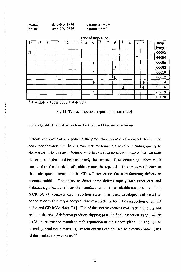
A typical inspection report as displayed on the monitor is shown in Fig 12 The
headline shows both the parameter set valid at inspection time and the current strip
number In the second line, the corresponding data for the next strip are displayed
The entire inspection width o f 1600mm is subdivided into 16 inspection lanes, each
o f which is 100mm wide In each o f these lanes, defect information is displayed for
channel 1 and 2 Included in Fig 12 are samples o f most possible defect types along
with their corresponding symbols In addition to the com piled inspection data, the
printed defect map includes reports regarding the condition o f the entire inspection
system
31
actual stnp-No 1234 parameter =14preset strip-No 9876 parameter = 3
zone of inspection16 15 14 13 12 11 10 9 8 7 6 5 4 3 2 1 strip
length□ 00002
□ ♦ 00004♦ 00006
+ 00008* 00010
* n 00012♦ * 00014
□ ♦ 00016* 00018
00020*,+, ♦ * - Types of optical defects
Fig 12 Typical inspection report on monitor [30]
2 7 2 - Quality Control technology for Compact Disc manufacturing
Defects can occur at any point in the production process of compact discs The
consumer demands that the CD manufacturer bnngs a disc of outstanding quality to
the market The CD manufacturer must have a final inspection process that will both
detect these defects and help to remedy their causes Discs containing defects much
smaller than the threshold of audibility must be rejected This preserves fidelity so
that subsequent damage to the CD will not cause the manufacturing defects to
become audible The ability to detect these defects rapidly with exact data and
statistics significantly reduces the manufactured cost per saleable compact disc The
SICK SC 60 compact disc inspection system has been developed and tested in
cooperation with a major compact disc manufacturer for 100% inspection of all CD
audio and CD ROM discs [31] Use of this system reduces manufacturing costs and
reduces the risk of defective products slipping past the final inspection stage, which
could undermine the manufacturer’s reputation in the market place In addition to
providing production statistics, system outputs can be used to directly control parts
of the production process itself
32

Each stage of CD production contributes unique defects which the inspection
computer can characterise and statistically summarise A brief catalogue of CD
defects which must be detected include
• Damage to the information surface
• Damage to the surface on the read side
• Bubbles or inclusions in the substrate material
• Metalisation defects, either single or several minor defects within a small area
A CD inspection system must reliably detect all these type of defects, and it must be
able to classify these defects and provide a measure of defect size The inspection
itself consists of three major components An optical scanner, a receiver system and
the electronic evaluation system A block diagram of the complete system is shown in
Fig 13
The optical scanner scans a fine point of light from a HeNe laser along the disc radius
As the disc is rotated, the entire disc is scanned Laser light striking the surface at an
angle to the disc is unsatisfactory Internal reflection within the substrate may cause
distortion of the size and position of the defects The telecentric design of the scanner
eliminates these problems by scanning normal to the disc surface along the entire
radius of the disc The receiver system is essential for recognising and classifying
defects The optical principle in the inspection of compact discs is based on the fact
that various orders of diffracted laser light can be used in a selective receiver system
The electronic evaluation system is designed to achieve maximum flexibility as well as
to rapidly process large amounts of data in order to inspect and classify the defects at
a rate of one CD per second The system creates a spatial raster of the CD in the
direction of scanning, which is used to determine the size and location of defects
The defect classification matrix determines how electionic signals will be intei pi ctcd
in order to classify the defect type
33

S cann er { T ra n s m it te r )
Fig 13 Block Diagram of CD Inspection System [31]
34

Defect information is stored on a 15 megabyte hard disk for production reports The
predefined reporting modes include current order, shift, and monthly reports The
defect statistics and system parameters are of special interest for the control and
optimisation of the production process The inspection computer may be linked to the
plant computer via standard communication protocols Thus the information from the
inspection system may be linked to other types of plant information In addition to
the high speed production mode of operation, the system can also run in a special
record mode In this mode a detailed defect map is produced for each disc when it is
inspected The process engineer can verify proper operation of the system, or make
minor adjustments to the sensitivity This is a great aid to fine tune the system after a
process change, or for quickly checking system performance for defect detection and
defect classification using standard, defect containing test CD’s
2 7 3 - Other applications of laser scanning inspection systems
There are many other applications for laser based inspection systems Some of these
include
• Laser scanners in tunnel inspections [32]
• Optical inspection of female contact’s defects for multipm printed circuit
connectors [33]
• Monitor of dimensions in the extrusion of plastics [34]
• Characterisation of silicon surface defects by the laser scanning technique [35]
• Photographic film inspection [27]
• Internal cylinder bore inspection [36]
• Laser scanning microscopes [37]
35

CHAPTER THREE

CHAPTER THREE
3 1- Inti oduction
In this chaptei the design and development o f the system used in this pioject to cany
out the expenm ents are leviewed The fust pait o f this chaptei deals with an
overview o f the complete system The puipose of this is to give an oveiall pictonal
view o f the system and then through the use of a block diagram describe geneially
how the system is controlled The block diagiam should also give an indication o f
the vanous pieces o f equipment used in the piocess, and the function each fulfils
Finally, each item o f equipment used is discussed in detail giving diagiams,
specifications and explanations as how each item o f equipment is operated to its
optimum capability
3 2 -Ovei view o f system
Fig 14 and Fig 15 are photographs o f both the system itself, and the type o f sample
plates used for measurements However, from the block diagram (Fig 16 ) it can be
seen that the complete system consists o f sub-systems They are, the sensor
(measurement system), the plotter, and the software needed to control the system
Each of these pieces o f equipment will be discussed in detail farthei on in this
chapter For the moment it is enough to describe the function they fulfil and how
they interact together As can be seen the automated operation o f the rig comes from
the PC terminal From this point all the other major parts o f the system can be
operated The plotter controls the movement o f the sample plate and the plotter
movement is controlled through the PC Therefore, when the movement o f the
plotter is discussed at any point what is really being referred to is the movement o f
the sample plate This movement is accomplished by either a written program or
using AutoCAD The operation o f the sensor is mainly controlled by software
loaded on the PC Any lateral movement o f the sensor must be done manually
However, all the movement
3 - Design and development of the Inspection system
37

Fig 14. Photograph o f the complete system in operation
Fig 15. Selection o f Brass, Copper, Polycarbonate and Stainless Steel sample plates
38

BLOCK DIAGRAM OF RIG
Movement of Sample Plate
Fig 16 Block diagram of Rig

we require for these experiments is done by the plotter Finally, all the output of
results is saved and manipulated in the PC terminal
3 3 - M easuring system
There are two main options in the structure of the measuring system (Fig 17 ) In the
first option (Al) the sensor is connected directly to a power supply unit that can give
a read out of both the analog and digital signal In the second option (A2) the sensor
is connected to a PC through an interface card As the digital signal is the one of
most importance for this project the second option is the system used in this project
However, preliminary tests were carried out using the first option in order to test the
suitability of the sensor It is clear from Fig 16 there are three main hardware parts
to the system Each of these parts will be discussed in turn
Structure of the Measuring System
220 Vac O
SENSOR
ILISensor cable-------------------- Power supplyC 2000-3 unit
PS 2000Al
+12 +5 Vdc
SENSOR
Sensor cableILD 2005
C 2001-3Interface card 1 ~ NHIFPS 2001
AT-Bus A2
Fig 17 The two options for the structure of the measunng system
40

3 3 1 - Lasei Sensor
The fust and most impoitant piece of haidwaie in the mcasunng system is the lasei
scnsoi itself The type ILD-2000 sensoi opeiatcs on the puncipal of optical
ti langulation Fig 18 is a pictonal diagiam of this sensoi that gives a view of the
\ ai ious paits and opeiation o f the scnsoi
Fig 18 Diagram o f Operation of optoNCDT sensor
From this it can be seen that a visible point o f laser light is projected onto the suiface
o f the target The diffuse part o f the reflection of this point of light is piojected onto
a CCD array by a receiving lens arranged at an angle to the optical axis The
intensity o f the diffuse reflection is determined in real time from the CCD signal
This allows the sensor to stabilise fluctuations in intensity during measurement over
a very wide reflection factor range (from almost total absorption to almost total
reflection) A high degree o f immunity from interference is achieved by early
digitisation o f the signal The signal processing offers the possibility o f adapting the
sensor to material surfaces through the digital interface This achieves a high
41

♦i CC
O lin
elinearity even on weakly reflective materials (e g black rubber) The measured
value is output simultaneously in analog (+\- 5V) and digital (RS485/687 5 kBaud)
foimat LEDs on the sensoi signal “Out o f Range” (uppei and lovvei lange values), a
non-measuiable taiget (leflection too low) “Pooi Taiget and Lasei ON/OFF A
block diagiam o f the sensoi can be seen in f ig 19
£J LasercontrolSoflslart
i k+ 24 Vdc *+ 12 Vdc + - - 12 Vdc « -
± analog 4 — + 5 Vdc < —
J. digital <4—Signalconditioning
----y AGC ADCControl signafor laser
Poortarget range
< + 24 Vdc< + 12 Vdc< -1 2 Vdc< _L analog< + 5 Vdc< JL digital
screen
RESET
Sensor cable connector
-G-J-C- R-I-A
-S
-P
-O
NM
UT
44 MHi
Fig 19 Block diagram of ILD 2005 sensor
42

In oidei to examine the capabilities and limitations of this scnsoi the following table
gives its chaiactenstics Aftei the table follows a descuption of influences that might
cause an enoi in the output of the sensoi and how to optimise the petioimance of the
scnsoi
Table 2 Specifications of the scnsoiMODEL ILD2005 SENSOR SpecificationsM easuung Range +/- 2 5mmStand off distance 58 mmNon Lm eailty 0 03% FSO +/- 1 5 pmResolution 0 005% FSO 0 25 pmTem peiatuie stability +/- 0 lpm /KLight souice Semiconductoi laser 670nmSmallest light spot size SMR 50 (.im
EMR 130pmSampling rate 10 kHzAngle error at +/- 30° Tilting at the X oi Y axis
typ +/- 0 5%
Angle en oi at +/- 15° Tilting at the X or Y axis
typ +/- 0 13%
Permissible incident light for direct radiation o f a diffusely reflecting target
30,000 lx
Piotection IP 64 (with connected cable)Opeiating temperature 0°C - 40°C (with free circulation)Storage temperature -20°C - 70°COutput analog +/- 5V/Rl > 1 kOhm
Digital RS485/687 5 kBaudPower supply through accessory 4 supply voltages requiredpower supply unit PS 2000 +5 Vdc/500 mA, +12 Vdc/250 mAor Interface card IFPS 2001 -12 Vdc/120 mA, +24 Vdc/30mA
3 3 1 1 - Tj icmgulation Method
The most common technique used in laser inspection systems for defect recognition is
the triangulation method It is also the method used by the optoNCDT sensor in the
system Optical triangulation provides a non contact method o f determining the
displacement of a diffuse surface Fig 20 is a simplified diagiam of a laser based
system that is successfully used in many industrial applications A low power HeNe or
43

diode laser projects a spot o f light on a diffusive surface A portion of the light is
scatteied fiom the surface and is imaged by a converging lens on a linear diode an ay 01
lineal position detector If the diffusive suiface has a component of displacement
paiallel to the light incident on it fiom the lasei the spot o f light on the surface will
have a component o f displacement paiallel and peipendiculai to the axis of the detectoi
lens
The component of displacement perpendicular to the axis causes a conesponding
displacement o f the image on a detector The displacement of the image on the
detectoi can be used to determine the displacement o f the diffusive suiface, thus any
surface defect will give a different leading to that of the normal suiface
Frg 20 Dtagram of laser based optical trrangulatron system
Many triangulation systems are built with the detector perpendicular to the axis of the
detector lens, Fig 20 The displacement Ad of the image on the detector in terms of
44

the displacement of the diffusive surface Az paiallel to the incident beam (1) is
appioximately
Ad = Az m sinO (1)
whcie m=i\o is the magnification factoi and is the angle between a line noimal to the
suitace and the light scatteied to the imaging lens Eqn (1) assumes the Az is small and
that 0 lcmams constant as the suifacc is displaced Thus we can use the appioximate
Eqn (1) to design an optical tnangulation gauge, we cannot, howevei assume that the
equation is exact Aftei the gauge is built it must be calibrated by displacing a diffusive
surface by known distances and deteimining the actual image displacement on the
detectoi A computei can be inteifaced with the detectoi and piogiammed to determine
the displacement o f the diffusive suiface from the displacement of the image on the
detectoi
Lasei-based tnangulation systems o f this kind are extensively used in industiy One
such application foi such systems is to determine the level of molten metal m a pour
box By using an optical triangulation unit mounted on the aim of a robot, propel
stand-off distance can be maintained so that the robot can perform operations such as
welding and painting
However, if a two dimensional measurement system is required using the laser-
based tnangulation method we must introduce the method o f projecting the line o f
laser light onto a surface using a two-dimensional detector With the mtroductron o f
computer vision into industry, systems o f this type are now available from several
vendors The system illustrated in Fig 20 can make dimensional measurements m
the x and z directions To produce the laser lrght lme on the part to be measured, a
cylindrical lens is used This lens extends the light in one direction, but not in the
other The Scheimpflug principle can be used to place the detector at the proper
angle to maintain the best laser light line image focus on the detector Note that the
system is not designed to make measurements in the y direction Tnangulation
devices o f this type are used to make measurements o f the depth and width o f seams
and gaps in sheet metal
45

3 3 1 2 - Diffuse reflection technique
Real reflection is a combination of diffuse and direct reflection In principle, the
sensor detects the diffuse pait of the reflected laser light (Fig 21 ) However, it is not
possible to make a definitive statement on the minimum reflection factor because
small diffuse parts can still be detected even from mirrored sui faces This is done by
determining the intensity of the diffuse reflection from the CCD array signal in real
time and then stabilising the fluctuations in intensity To use the sensor on transparent
or reflective objects, manufacturer pre-testing is necessary
Laser beam
Ideal diffuse reflection
Laser beam
Real reflection, usually mixed
Fig 21 Principles of diffuse and real i eilcction
46

3 3 I 3 - E nor Influences
Diffcrcuccs in Culoui
Differences in the colour of targets effect the measuring result of the ILD 2000 only
slightly due to the intensity adjustment However, these differences in colour are
often combined with different penetration depths of the laser light Different
penetration depths also cause apparent changes in the size of the measuring point
Therefore, changes in colour combination with changes in penetration depth can
result into measuring errors This phenomenon also effects the linearity behaviour of
the sensor if it has been adapted to white diffusely reflecting refeiente matcnal If,
on the other hand, the sensor is optimised for black matcnal, a much better linearity
behaviour is achieved
Tempcratuic Influences
The internal housing temperature of the sensor is measured by an integral temperature
sensor and so the measured displacement values arc tempeiaturc-compensated A
warm-up time of at least twenty minutes is necessary before taking data in order to
achieve a uniform temperature distribution in the sensor If measurements are to be
made in the micron accuracy range the effect of the temperature fluctuations on the
sensor must be considered Fast temperature changes are damped by the sensois heat
capacity
Mcchniucnl vibiations
If the sensor is to achieve resolutions in the micron to sub-micron range, particular
attention must be paid to a stable or vibration-damped sensor and target installation
Suifacc Roughness
Suiface roughness of 5 micron and above creatc an appaicnl changc in distance it the
surface is scanned (also called surface noise) These can be sui pressed by the
technique of averaging
47

Ambient light Iniluciiccs
Due to the narrowband optical filter used, measurement can be made reliably even
when a diffusely reflecting target is exposed to direct sunlight
Angle Iniluciiccs (Fig 22 )
Angles of tilt of the target around both the X and Y axis of less than 5° only causes
errors with sui faces giving strong direct icflection Angles of tilt between 5° and 15°
cause an apparent change in distance of approx 0 1% of the measuring range 1 hese
influences must be noted particularly when scanning structured sui faces In pnncipal
the angle behaviour is also subject to the reflectivity of the target sui face
Angle X axis Y axis5° 0 04% 0 03%15° 0 12% 0 1%
w o o 0 5% 0 5%
Fig 22 Angle Influences
Optimisation o f the measuring accuracy by special sensor arrangement
In the case of rolled or polished metals moving past the sensor, the sensor plane must
be orientated parallel to the direction of the rolling or gnndmg niaiks The same
arrangement should be made for coloured stupes (Fig 23 )
48

Direction of movement Colour lines 1
Grinding or rolling marksILD2005
Fig 23 Sensor arrangement for ground or striped surfaces
In the case of drilled holes, recesses and ndges in the surface of a moving target, the
sensor must be arranged so that the edges of these features do not obscure the
backscattered light (Fig 24 )
ILD 2005
Fig 24 Sensor orientation for holes and ridges
49

3 3 2 - Power Supply Unit PS 2000
The PS 2000 powei supply unit piovidcs the voltages nccessaiy foi opeiating a
maximum oi two types ILD 2000 scnsois 1 his powei supply unit was used in the
initial expenmcntal stages to examine the analog output 1 he output signal is g i\cn
as a voltage in the +/- 5V lange at the two analog outputs Fheic is the possibility if
needed, o f connecting up the unit to an intei face caid in oidei to examine the digital
signal A block diagiam of this powei supply with some o f Us technical data can be
seen on the following page in Tig 25
3 3 3 - Intei face C aid lT PS 2001
This card provides one RS485/687 5 kBaud interface It has an integrated powei
supply for operating an ILD 2000 sensor The sensoi and the card are connected by
means o f the C2001-3 sensor cable The powei supply and thus the sensor is
switched on or o ff and the data transfer is carried out by the software or program
modules A diagram showing the layout o f this interface card can be seen below in
Fig 26
Interface Card IFPS 2001
♦ 12V 4 w r Y-caWe 16*BIT-Bu®
Electrical Isolation
8CMCOQ_
Power supply In V j_ Interfaoe
♦5 *1A 12 412 Aiuloo Digital 1 1
—w3ESET RS465 RS485
PC
15 pinHD-submlniature connector
5O 2 SO 3 EÛ AO S
eRESET
O 0 ♦5 VO T ♦24 Vo e 12V y—
O 9 *12 V i_Q
O 10 AnMog 1 tnaO 11 Afmfeg »(guai
O 12 Anafog Signal _ L 0)O 13 NC wO H OlgHaLL
^ 1 5 ^ Scie€n
Fig 26 Block diagram of Interface card IFPS 2001
50

Block Diagram - Power Supply Unii PS 2000
Analog Analogoulput 1 output 2
Fig 25 Block diagiam of I’owci supply unit I’S 2000
si

3 3 4 - Measured value output
Analog
After putting the sensor into operation, the displacement signal is available as an
analog voltage value in the range +/- 5 V
• the sensor output may only be loaded with IlL > 1 kOlim
• this analog signal is filtered through a 100 kHz low pass filter at the output of the
power supply unit PS 2000
• the output has internal resistance of R, = 250 Ohms
• the erroi is 1 3 mV at the end of the measuring range at a load icsistancc of RL =
IMohm
Digital
After putting the sensor into operation, the aveiaged value is available at the output
of the serial interface in the range 0 65535
• 0 1637 - measunng value out of range (*)
• 1638 - 63896 - measunng value in the range (*)
• 63897 65534 - measunng value out of range
• 65535 » Poor Target « - no range
(*) Both measuied values no longer correspond to the sensor specification They are
used for adjustment in order to slightly exceed or drop below the measured value
An example of the signal output given from the sensor can be seen in Table 3
52

Table 3 Signal output of the sensor
Description LED on the sensor Analog output Serial InterfaceLaser in operation Green -Laser On/OffTarget does not reflect sufficiently Penetration depth of the laser point too deep - corona formation too great
Red - Poor Target output > +5 26V or last valid measure
output 65535
Target still in detection range but slightly beyond the measunng range
Red - Out Of Range output-5 00 -5 26V or +5 00 +5 26V
output 0 1637or 63897 65534
No target available Red - Poor Target Red - Out Of Range
output > +5 26V or last valid measured value
output 65535
3 4 - X-Y kinematics system
The objective of this system is to facilitate the movement of the sample being
measured It should fulfil the role of an X-Y table system In effect we wish to be
able to manipulate the sample plate in the X and Y direction using a scanning motion
This eliminates the requirement to move the sensor itself, thus simplifying the
kinematics
3 4 1- Roland DXY 1300 plotter
This piece of equipment was used to achieve the required movement in the X-Y plane
All aspects on the operation of this equipment, and how it controls the sample plate,
will be discussed in the following sections One extremely important point of note is
that the sample plate is mounted directly onto the pen carnage of the plotter
Therefore, any discussion of the movement of the pen carnage is in effect refemng
also to concurrent movement of the sample plate Fig 27 gives two separate views of
the plotter
53


s€Ooî.

Having obtained an overall idea of ihc shape and movement of the plotter it is
impoitant to sec the main features of the plotter Fig 28 gives a side view and a look
at the rear panel of the plotter A description of the operational features can be seen
in Appendix A
Sido View
Rear Panol
(y Parallel connoclor (centronics)
Q) Sena! rotm eclur(FIS 232C intoilaio)
0 sw i luir swiilm ii <y sw 2 tuir swmh ¿1
l'ig 28 Some of (lie iim iii opci.ilion.il lunUioiis

3 4 2 - Automatic control of the plotter
There are two separate methods for controlling the plotter other than its manual
controls They consist of either plotting a drawing from AutoCAD or by direct
programming of the plotter using a program written under BASIC The operations
used for each of these methods will be discussed in detail giving emphasis to the
particular solutions used for this project
3 4 2 1 - Control by AutoCAD
As has been mentioned previously, the sample plate to be measured is connected
directly to the plotter pen carnage So when a drawing is sent to the plotter the
sample plate moves in unison with the carnage The sensor is mounted above the
plotter drawing board at an arbitrary static position When the sensor is switched on a
red beam of light strikes the plotter below Therefore, the motion of the plotter
represents the scanning motion of an X-Y table The X-Y coordinate display on the
plotter control panel gives the coordinates of the plate at any moment in time
Therefore, using these pieces of information it enabled the calibration of plotting a
drawing from AutoCAD to coincide with any particular area of the plate we wish to
scan The easiest way to illustrate this is by means of a typical example
An example of a typical sample plate is given below in Fig 29
130mm
A B
Surface defects
60mm
oc D
Fig 29 Diagram of sample plate
56

The dimensions of the plate are 130x60mm and there are surface defects of different
shapes and sizes placed randomly throughout the plate For the purpose of this
project we wish to be able to scan the surface starting at point A and finishing at point
D The most economic way to achieve this is to scan in straight lines The first line is
from point A to point B Then a step down is taken a certain distance and the second
scan line begun in the opposite direction to the first This process is repeated until it
finishes with the last line from C to D The step size moved down each time is
predetermined depending on certain parameters (eg size of smallest defect,
specifications of plotter etc )
An example of a drawing plotted from AutoCAD to achieve this purpose is given
below in Fig 30
A _________________ B
StepSize T D
Fig 30 Plotted AutoCAD drawing
Plotting this drawing achieves the purpose of scanning the sample plate as described
above The location of the points A,B,C and D coincide with the same points from
the edges of the plate (Fig 30 ) The method of achieving this end is described at the
start of this section Once the points A to D have been located the only other task is
to specify a step size The main consideration for this problem is to assure that the
steps are small enough so as not to miss any of the defects For this either need prior
knowledge of what size defect is being sought, or a cut off criterion as to the
minimum size defects permissible It should also be noted that a knowledge of certain
drawing parameters is crucial to assure the accuracy of the plotted drawing For
example when the drawing is plotted we must know what scale the drawing is in
relation to real (mm) units
57

3 4 2 2 - Formula fo r calculation o f scanning parameters
L - Total length of the scan line (mm)
P - Plotter speed (mm/s)
T - Total time for entire scan (secs)
S - Sampling rate of sensor (Hz)
V - Total number of values to be measured
In order to calculate [L] we need to know three measurements They are step size,
scan length and the total number of steps taken (Fig 30 )
L = (Length CD x Number of steps) + (Step size x Number of steps)
Once we have calculated L and set the value for P we can calculate T
L (mm) / P (mm/sec) = T (secs)
Having calculated T and set the value for S then we can calculate V
T (secs) x S (Hz) = V
There are two main advantages of using AutoCAD for moving the plotter The first
of these is the ease with which we can change the step size of the line scan As stated
above once we know the location of the perimeter points A to D we can easily change
the step size in the drawing to suit our needs The second advantage is the ability to
change the pen speed/scan speed for different experiments In fact AutoCAD
possesses the ability to vary the speed in forty two different steps from 14mm/sec up
to 420mm/sec In order to do this all that is required is to change the pen speed
assignments before sending the drawing to the plotter However these actual speed
values had to be worked out manually using a ruler and a stop watch A full list of the
actual speeds of each pen is given below
58

Table 4 Pen speeds avai able using AutoCADPen No 1 2 10 20 30 42Pen speed (mm/sec)
14 20 100 200 300 420
3 4 2 3 - Control through command system
This is the second method we have for controlling the plotter through the computer
The DXY 1300 series comes with two internal command systems DXY-GL and RD-
GLI The plotter can be used by selecting either of them The DXY-GL and RD-GL
I commands have the following characteristics
DXY-GL Commands
• There are 22 types of command
• Each command executes completely without the need of others
• They make the creation of programs quite easy
• They are compatible with Roland DG’s DXY plotter commands
• They have a certain degree of compatibility with Roland DG’s CAMM-GL I
command system for the CAMM-3 modelling machine and CAMM-GL II
command system for the CAMM-2 engraving machine
• They can call RD-GL I commands into use
RD-GL I Commands
• There are 56 types of command
• Several commands must be combined to execute one action
• They make programming somewhat difficult
• They permit high definition
• They are compatible with Roland DG’s RD-GL plotter commands
59

The function of this software is to make it possible to take measurements using the
sensor ILD 2005 under WINDOWS This program was written for propagating the
use of the sensor but it was not used in processing or data acquisition systems There
are certain limitations in measuring parameters by running the package under
WINDOWS
• The maximal sampling rate under WINDOWS is 1kHz
• The minimum sampling rate is now 1Hz
• The number of data elements is limited to 8000
3 5 1- Software Configuration
From the software package wntten by Micro-epsilon (Germany), there are five
separate menu headings to choose from Each of these headings in turn has a few
different possibilities In order to understand how to work this software package the
first step is to explain what each heading does A full explanation of this package can
be seen in Appendix B Having explained the terms in Appendix B, an example of
the measuring process for both continuous measurement and spontaneous
measurement will be described
3 5 2 - Sample measurement process
Before running an experiment it is necessary to set certain conditions or options First
we select the sensor type being used In this case it is the ILD 2005, this indicates a
measuring range of 5mm Then there are a series of options The first option is
whether to acquire the data in decimal form or with the use of a comma It is usually
set to decimal form as this makes it easier to manipulate the data later Secondly a
TRIGGER can be set as to when to start the measurement This enables the user to
control the start of the measuring process Finally there are the options of changing
3 5 - Software s
60

the frequency limit or the number of averages for each measurement Once all of
these have been set the power can be turned on and the sensor is ready for operation
There are two ways in which measurements can be obtained They are single
measurement or continuous measurement For single measurement each time the
return key is pressed on the keyboard the program records the value being measured
at that point This method is useful at the initial stages of measuring, or if there is a
long discontinuity in parts where we require data However, this can become a
tedious process and is not very useful if it is not known where the defects are in the
sample Obviously a method of continuous measurement is much more desirable
Before starting the continuous measurement process it is necessary to define the total
number of measurements to be recorded and the sampling rate The total sample size
must be between 100 and 8000, and the sampling rate must be between 1Hz and
1kHz These limits, as discussed earlier are determined by the limitations associated
with running the sensor under WINDOWS The total number of measurements, and
the preselected sampling rate, will determine the duration of the measurement The
computer will acoustically signal the end of the measurement After the measurement
is complete the data can all be saved to a file This file can then be brought into any
other WINDOWS applications for further analysis There is also a facility to graph
and display various statistical data the data in the Windemo program
61

CHAPTER FOUR

CHAPTER FOUR
4 1 - Introduction
This chapter deals with the various experiments that were earned out on the system
and discusses the significance of the results obtained The chapter can be divided into
vanous different sections Firstly, the initial tests earned out on the system measured
the analog output tested on an aluminium plate These expenments were important in
deciding on the suitability of the sensor as a measunng device The following sections
deal only with the digital output Each section will deal with the expenmental results
for each different material used These materials will range from aluminium, stainless
steel, brass and copper through to polycarbonate and perspex Also, each section
contains detailed graphs of the results obtained These graphs will be discussed and
explained thoroughly as to their significance and meaning The first section of digital
results on aluminium contains a detailed example as to how the graphs are obtained
from the output information as well as a close look at the output information itself
The methods discussed in this section for manipulating the output information hold
true for all the other expenmental results
4 2 - Analog tests
An example of the aluminium plate used for these experiments is shown in Fig 31
X
direction of scan
4 - Experimental results and Discussion
Fig 31 Sample aluminium plate used in analog expenments
63

As we can see from Fig 31 The sample plate consists of a piece of aluminium with
eight separate holes The diameter of these holes varies from 25mm to 2mm
respectively The average thickness of the plate was approximately 2mm However
the plate had a slight curve in it so as it would not lie evenly on a flat surface The
sensor remained stationary above the plate as the plate was moved underneath it in the
direction indicated It was during this movement of the plate that the measurements
were taken
The main objective of this exercise was to observe how the sensor reacted to surface
defects and how it coped with different degrees of reflectivity of the surface type The
analog output from the sensor is in the range +/- 5V and the sensor has a measuring
range of +/- 2 5mm A typical measured output for the experiment is given in Table
5 below
Table 5. Analog output for aluminium plate
Hole Diameter (mm) A (Volts)
[Before]
B (V)
[Across]]
C ( V )
[After]
25 0 004 4 54 0 692
20 -0 9 3 74 -0 9
1 7 5 -0 9 4 48 -0 78
15 -0 78 4 138 -0 68
10 -0 62 4 152 -0 454
7 5 -0 424 4 344 t o to
4 -0 066 4 176 -0 06
The scanning across each defect is represented by the measured output analog
voltages at A,B and C Where A is measured just before a defect, B is measured
across the defect itself, and C is the measurement just after passing the defect The
results of the analog test can be displayed as a 2D graph (Fig 32 ) This graph shows
the sensitivity of the sensor The voltage can range from -5V to +5V It represents
the sensors measuring range of +/- 2 5mm
64

2D graph of analog results
Fig 32 2D Graph of Analog test results on Aluminium plate
Each of the seven peaks that appear in the graph indicate the sensor's ability to detect
each of the seven different size defects This simple experiment was used to assess
the sensors' ability to detect surface defects Having been satisfied that the sensor has
a suitable measuring range and capability, the next set of experiments to be
performed were the digital expenments
65

4 3 - Aluminium digital tests
4 3 1- Selection of initial measuring parameters
This is the first experiment to be earned out when the entire system was up and
running automatically As such a detailed analysis of the entire measunng process, as
well as the results, will be presented The aluminium sample plate had dimensions
100x120x2 5mm It was mounted on the pen carnage of the plotter (Section 3 4 1)
The surface defects consisted of four separate hole with diameters 2,3,4 and 5mm
respectively It was decided to only scan an area of 79x75mm because all the defects
were inside this area
The next step before starting the measunng process is to determine certain measunng
parameters Once the scan area had been determined then an appropnate drawing in
AutoCAD was plotted to accommodate this scanning area (Fig 33 ) For the initial
testing a step size of 5mm was used Therefore, fifteen steps (15x5) were necessary
to accommodate the Y direction of 75mm The coordinates for the edge of the plate
were made to coincide with the start of the scanning pattern
B
StepSize
iT D
Fig 33 Plotted AutoCAD drawing
A sampling rate (S) and plotter speed (P) have now to be selected A nominal plotter
speed of 14mm/sec was selected A sampling rate of 28Hz was then selected after the
plotter speed had been determined Using this sampling rate ensures that a data point
was taken for every 0 5mm scanned The mam reason for choosing these values was
66

to ensure that the smallest defect we are looking for is detectable The entire length
of the scan (L) is calculated as = 79x16 + 15x5 = 1339mm Using the formulas
derived in chapter three and knowing the above values it is possible to calculate the
total time it takes for the scan (T) and the total number of measurements (V) to be
taken In this case they were calculated to lie 95 64secs and 2678 respectively An
important point to note is the healthy balance which must exist between S,P and L
For instance, V and S have limits of 8000 and 1000Hz respectively Also the
maximum speed capability is 420 mm/sec Due to these limitations, and in order to
reduce scan time, the optimum balance of the parameters was restricted
In summary the set scanning parameters for this test were
Plotter speed (?) = 14mm/sec
Sampling rate (S) = 28 Hz
Length of scan (L) = 1339mm
Total scanning time (T) = 95 64secs
Number of values to be measured (V) = 2678
The only other parameter which had to be set before starting the measurement
process was the trigger condition The function of the trigger condition was to start
the measurement process at a certain chosen point For these experiments the option
‘trigger from infinity’ was used This ensured that the measurement process
commenced only when the sensor came within the measuring range This of course
coincided with the edge of the sample plate
4 3 2 - Representation of output signal
When the above conditions had been selected able the measurements were started
The output from the sensor was in the form of depth measurements, obtained using
the tnangulation method (as described in section 3 3 1 1 ) As set previously the
number of values to be measured was 2678, therefore an output of 2678 distinct Z
coordinates was obtained A full list of the output received for this experiment is
67

shown in Appendix D The readings commence at point A1 and continue down to
A47 Then the next step is B1 to B47 This method is consistent until the final
reading is reached which is located at BK15
One method of representing all of the recorded information is in the form of a 2D
graph This helps give a clearer picture as to the meaning of all the output
information Fig 34 below is a graph of all the measured data for the aluminium test
Grid Reference Points
Fig 34 2D Graph of Aluminium test results
The first points to note about the graph (Fig 34) are the X and Y axes The Y-axis
consists of depth measurements in mm The X-axis consists of grid reference points
Therefore each reference point indicates a particular set of coordinates on the sample
plate For example the data point 198 might represent a point (64,5) on the sample
plate Each grid reference point on the graph is taken from Appendix D Given the
scanning parameters, the values 1 to 158 constitute the first scan line from
coordinates (0,0) to (79,0) and that the next 10 values are from (79,0) to (79,5) The
relationship between the grid reference points and the plate coordinates can be
68

calculated from the scanning parameters An example of this system is shown in
Table 2
Table 2 Relationship between output and coordinate system
Plate coordinates Grid reference points Location in App D
(0,0) (79,0) 1 158 Al D17
(79,0) (79,5) 158 168 D17 D27
(79,5) (0,5) 168 326 D27 G44
(0,5) (0,10) 326 336 G44 H7
(0,10) (79,10) 336 494 H7 K24
(79,10) (79,15) 494 504 K24 K34
(79,15) (0,15) 504 662 K34 04
(0,15) (0,20) 662 672 04 014
(0,20) (79,20) 672 830 014 R31
(79,20) (79,25) 830 840 R31 R41
(79,25) (0,25) 840 998 R41 V il
(0,25) (0,30) 998 1008 V il V21
(0,30) (79,30) 1008 1166 V21 Y38
The most important point to observe from the graph (Fig 34 ) is the four large peaks
located approximately in the centre of the graph These correspond to the location of
the four holes in the aluminium plate A sample of the data which represents the
smallest defect is highlighted in Fig 35
S T U V W X Y Z AA1 -0 8806 -0 9004 -0 8475 -0 8603 -0 8453 -0 8109 -0 8526 *0 8406 -0 86542 -0 8882 -0 9025 -0 8507 -0 8582 -0 8429 -0 8084 -0 8482 -0 829 -0 87593 -0 8041 -0 8968 -0 848 -0 86 : -2,0315 >0 8008 -0 8502 -0 8401 -0 8734 -0 8592 -0 8898 -0 8417 -0 8564 -2,6315 -0 7991 -0 8502 -0 8431 -0 86915 -0 8629 -0 8981 -0 84 -0 8568 -26315 -0 8068 -0 8504 -0 8242 -0 87026 -0 8678 -0 8938 -0 84 -0 8568 -0 8561 -0 8059 -0 8565 -0 8244 -0 8706
Fig 35 Extract of results table in Appendix D displaying depth values in mm, with
the values for the smallest defect highlighted
69

The height of these peaks in the graph corresponds to the depth of the holes The
holes in the plate were approximately 2 5 mm in depth If the surface of a plate was
giving a negative reading of -0 5 and the hole has a measured depth of 2 5mm from
the surface, then theoretically the bottom of the hole should give a reading of 3 0
However, the measuring limit of the sensor is -2 6, so the reading that shows up for
the bottom of the hole would be the sensors bottom limit of -2 6
The diameter of each of the holes can be calculated from the number of data points
recorded at these coordinates when compared with the speed of the scan and the
sampling rate For example with the plotter travelling at a speed of 14mm/sec and a
sensor sampling rate of 28Hz this means each recorded value from the sensor is
0 5mm apart So if the sensor measures 12 values for the spike, this indicates a hole
diameter of 6mm
As an indication of this fact we observe the data points W3 to W5 (Fig 35 ) These
three maximum values correspond to the smallest hole of approx 2mm in diameter
The fact that there are three values instead of four may seem to indicate that the
sensor miscalculated the hole diameter as 1 5mm There are two main reasons for this
error There may be a margin of error associated with process of drilling the holes in
the plate The other reason relates to the speed and sampling rate There can be no
guarantee that the first value W3 corresponds exactly to the edge of the hole What is
more likely is that it corresponds to a point 0 2-0 3mm inside the edge of the hole
Therefore, if the readings are occurring every 0 5mm, then three readings later it
should have passed by the other side of the defect So, it is logical to assume a
margin of error of 1 value as to the actual size of the defect In this case, adding one
on to the three readings already recorded gives a hole diameter of 4x0 5 mm = 2mm
and this indeed corresponds to the actual diameter of the hole
1The location and number of values of the other three defects are
1 W41 —» W46 6 values
2 X34 -> X40 7 values (+1 for error)
70

3 Y27 —> Y35 9 values (+1 for error)
Using the method discussed above for calculating the hole diameter and allowing for
the errors also discussed, the sensor gives hole diameters of 3,4,5mm which
corresponds to the actual diameter of the holes
4 3 3 - Coordinate system
An important point to notice is that the grid reference point gives the exact location of
these defects The actual location of these defects is given below in Fig 36
(0,75) (79,75)
Fig 36 Actual coordinates/dimensions of sample plate
From the sensor output signal, the coordinates/dimensions were calculated using a
combination of the data from Appendix D and Table 6 Calculating the coordinates
using this method it was found that they corresponds almost exactly to their real
coordinates (Fig 37) An error of +0 5mm that occurred for the measurements
71

between the holes was due to the sampling rate Another possibility for error could
be due to the movement of the plotter which was smooth
(0,75) (79,75)
(0,0)
Fig 37 Coordinates/dimensions of sample plate calculated by the sensor
4 3 4 - Experimental errors
It has been explained in section 4 3 2 how the graph of the aluminium results (Fig
34) displays information about the sample plate Detail has been given of the
significance of the peaks in the graph shown in Fig 34 and how these peaks may be
used to obtain an overall picture of the sample plate However, no explanation has
yet been given as to why the rest of the graph is not perfectly smooth The first and
most obvious reason relates to the plate itself No matter how level the surface of the
plate might appear to the eye, it is not a perfectly smooth surface Therefore, a
certain amount of variation in the output is to be expected, especially when such a
small scale is used
72

Another error is caused by the way the plate is mounted Due to the fact that the
plate is only screwed to the pen carnage on one side and the selfweight of the plate, a
slight incline can arise, thus making the plate lopsided The significance of this
incline can be seen in Fig 38 and Fig 39 In order to assess how much of an incline
there was, the first scan line (points 1-158) and the second scan line (points 168-326)
were plotted respectively From Fig 38 it can be seen that the values start from -
0 875mm and move gradually upwards until they peak at roughly -0 8mm
Conversely in Fig 39 the values range from -0 8mm down to -0 875mm
The similanty of this variance indicated a slope of +/-0 075mm for every 79mm
depending on which direction being travelled in Or in other words a gradient of
0 05°
First Scan line
Fig 38 Graph of results for first scan line
73
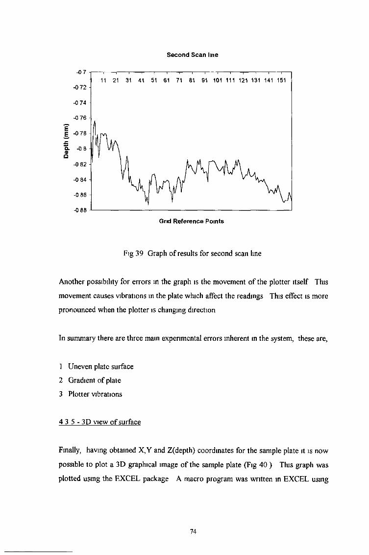
Second Scan line
Fig 39 Graph of results for second scan line
Another possibility for errors in the graph is the movement of the plotter itself This
movement causes vibrations in the plate which affect the readings This effect is more
pronounced when the plotter is changing direction
In summary there are three main experimental errors inherent in the system, these are,
1 Uneven plate surface
2 Gradient of plate
3 Plotter vibrations
4 3 5 - 3D view of surface
Finally, having obtained X,Y and Z(depth) coordinates for the sample plate it is now
possible to plot a 3D graphical image of the sample plate (Fig 40 ) This graph was
plotted using the EXCEL package A macro program was written in EXCEL using
74

Depth
(m
m)
Visual Basic in order to facilitate the manipulating of all the data into an appropriate
gnd system Details of this macro program can be seen in Appendix C
X-Coords
Y -C ooi
(0,75)
5 mmo o o(0,0)
Fig 40 3D Graph of aluminium plate compared to actual sample plate
(79,75)
(79,0)
75

However, this graph is not to scale as none of the values measured during each
stepping motion are plotted These were omitted in order to speed up the graphing
process and because they were not critical to the overall picture of the 3D graph
For the other materials tested it is not necessary to explain once again how certain
values and parameters were calculated It is enough to say that any method of
calculation or experimental technique used in the aluminium experiments were also
used in the other experiments
76

4 4 - Stainless Steel digital tests
The surface o f the material contained The first set o f these defects consisted o f 7
holes with diameters ranging from 7mm to 2mm in decreasing steps o f 1mm all o f
which had a depth o f 2 6mm The second set o f defects consisted o f 5 holes with
diameters ranging from 8,6,6,5 and 3 mm all o f which had a depth o f 0 6mm The rest
o f the materials tested after stainless steel were given the same type o f defect at the
same location in order to aid the examination o f the effect o f different materials The
scanning parameters were the same as those used for the aluminium experiments
These parameters were kept constant for all the digital experiments
After several tests all o f which proved consistent with one another the output was
once again first plotted in the form o f a 2D graph (Fig 41)
Stainless Steel Plate
Fig 41 2D Graph o f Stainless Steel test results
As can be seen from the graph (Fig 41 ), the first set o f defects show up around the
centre o f the scan It may not be very clear from the graph but there are four distinct
peaks as opposed to the six defects which are actually in the sample The four defects
77

which appear are the four largest defects Fig 42 gives a view o f the data points
1370 -» 1460 in order to get a clearer view o f these peaks The sensor determines
their depth and diameter using the same method as for the aluminium results The
reason that the other two defects do not appear in the graph is not because the sensor
was unable to measure them It is due to the scanning pattern determined at the start
o f the scan In the beginning it was determined to have a scan step size o f 5mm So
the defects o f 2 and 3mm unfortunately happen to have fallen in between scan lines
In order to ensure this does not happen it would be necessary to change the step size
to the smallest defect we need to find However, there are limitations to changing the
step size as it effects other scanning parameters (section 4 3 1 )
Stainless Steel Values 1370 to 1460
05
I -° S H
f 1 ,<D -1 'O
A 5
-2
-2 5
dl
11
d2
€1
d3
81
d4
Grid Reference Points
1370 1460
section ofsampleplate
Fig 42 Graph o f Stainless Steel results o f points 1370 to 1460 and their
corresponding plate coordinates
78
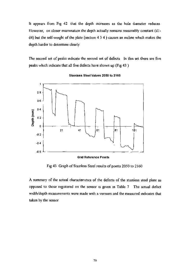
It appears from Fig 42 that the depth increases as the hole diameter reduces
However, on closer examination the depth actually remains reasonably constant (d l-
d4) but the self-weight o f the plate (section 4 3 4 ) causes an incline which makes the
depth harder to determine clearly
The second set o f peaks indicate the second set o f defects In this set there are five
peaks which indicate that all five defects have shown up (Fig 43 )
Stainless Steel Values 2050 to 2160
Fig 43 Graph o f Stainless Steel results o f points 2050 to 2160
A summary o f the actual characteristics o f the defects o f the stainless steel plate as
opposed to those registered on the sensor is given in Table 7 The actual defect
width/depth measurements were made with a verniers and the measured indicates that
taken by the sensor
79

Table 7 Calculated characteristics of the Stainless Steel plate
Scan line No Actual defect
width(mm)
Measured
defect width
Actual defect
depth(mm)
Measured
defect depth
9 7 6 5 2 6 2 6011
9 6 5 5 2 6 2 5881
9 5 4 2 6 2 5663
9 4 3 2 6 2 6134
9 3 - 2 6 -
9 2 - 2 6
13 3 2 0 6 0 5601
13 5 4 5 0 6 0 5726
13 6 6 0 6 0 6225
13 6 5 5 0 6 0 5972
13 8 7 5 0 6 0 5842
From Table 7 it can be seen that the sensor measures very accurately However,
there are some discrepancies between the vernier and the sensor values which should
be explained Some reasons have already been given as to why the sensor fails to
measure the smaller defects It should also be noted that there is no way of ensuring
that the sensor passes directly over the widest part o f any defect Added to the reason
already suggested in the aluminium results as to too large a step size, this gives a
margin o f error associated with the defect width Finally as regards the depth o f the
defect, the sensor is a much more sensitive measuring instrument than the verniers
and therefore measures the depth more accurately
Another main point to note about the graph (Fig 41 ) is its apparent sinusoidal nature
The reason for this is that it was mounted on a slope The effect o f this slope is more
pronounced than that in the aluminium results This is because the plate was mounted
on top o f the aluminium plate Therefore, the additional weight results in a more
exaggerated slope In fact the slope was calculated as 1 08° The good part about
this slope is that it makes it much easier to identify each line o f the scan
80

The surface o f the brass material contained two basic defects The first set o f these
defects consisted o f 7 holes with diameters ranging from 7mm to 2mm in decreasing
steps o f 1mm all o f which had a depth o f 2 6mm The second set o f defects consisted
o f 5 defects with diameters ranging from 8,6,5,4 and 3mm all o f which had a depth o f
0 6mm
The experimental settings/parameters were consistent with all o f the other digital
experiments A plot o f the typical results obtained can be seen tn Fig 44
4 5 - Brass digital tests
Grid Reference Points
Fig 44 2D Graph o f Brass test results
%
As before two distinct set o f peaks stand out in the middle o f the graph Graphs o f
these two important sections can be seen in Fig 45 and Fig 46 There is an important
difference between these results compared to those obtained with stainless steel The
first observation is that the defects have shown up m different scan lines The reason
81

for this is that the initial positioning o f the brass plate was slightly o ff to that o f the
stainless steel plate For this reason, the sensor commenced measuring during its
second scan line and so reached the defects at a different position in the scan This
slight change m positioning also affected the position at which the sensor crossed the
defects In fact it is likely that the scan line failed to coincide with the centres o f the
defects Confirmation o f this fact can be seen in Fig 46 On the bigger two defects o f
widths 8 and 6mm, they have shown up on the next scan line In other words these
defects fall on two different scan lines
Brass Values 1190 to 1323
1 5
I
05
09 17 2! 33 41 ¿9 57 65 73 &K4 9 97 105 113 121 129
-1 5
-2
-2 5
-3
Grid Reference Points
1190 1323
4mm
© 0 0section ofsampleplate
Fig 45 Graph o f Brass results o f points 1190 to 1323 and their corresponding plate
coordinates

Brass Values 1864 to 2135
Fig 46 Graph o f brass results o f points 1864 to 2135
Table 8 below gives a summary o f the characteristics recorded for the brass plate
Table 8. Calculated charactenstics o f the Brass plate
Scan line No Actual defect
width(mm)
Measured
defect width
Actual defect
depth(mm)
Measured
defect depth
8 7 6 5 2 6 2 7225
8 6 5 2 6 2 5264
8 5 4 2 6 >2 437
8 4 3 2 6 >2 2225
8 3 - 2 6 -
8 2 - 2 6 -
12 3 - 0 6 -
12 4 2 0 6 0 3167
12 5 2 5 0 6 0 5978
12 6 3 5 0 6 0 5256
12 8 7 0 6 0 5566
83
The initial alignment o f the plate is one o f the main reasons why the measured values
do not correspond exactly to the actual values It should be noticed that some o f the
measured depths could not be calculated as they extended beyond the maximum
measuring limit o f the sensor (section 4 3 2 ) Therefore all we can say with certainty
about these depths is that they are greater than a certain depth value Other errors
discussed earlier for the stainless steel and aluminium results also occurred with the
brass test plate The average gradient o f the plate was calculated to be 1 81° This
gradient is directly related to the self-weight o f the plate and also a cause o f error
4 6 - Copper digital tests
The surface o f the copper material contained two basic defects The first set o f these
defects consisted o f 7 holes with diameters ranging from 7mm to 2mm in decreasing
steps o f 1mm all o f which had a depth o f 3 5mm The second set o f defects consisted
o f 5 defects with diameters ranging from 8,6,5,4 and 3mm all o f which had a depth o f
0 6mm These defects were similar in both position and size to those o f the brass
plate, the only difference being the depth o f the holes
The experimental settings/parameters were consistent with all o f the other digital
experiments A plot o f the typical results obtained can be seen in Fig 47
\
84

Grid Reference Points
Fig 47 2D Graph o f copper test results
The first point to note about Fig 47 is that it bears a strong resemblance to the
stainless steel results presented in Fig 41 The position on the graph o f where the
defects appear is almost identical to that recorded for the stainless steel plate This is
due to an almost identical positioning o f these plates during the set up procedure A
closer inspection o f the defect areas can be seen in Fig 48 and Fig 49 It can be seen
that once again the smallest two defects in the first set o f holes has again been missed
This is mainly due to the step size selected However all o f the second set o f defects
have shown up Again these two graphs show a strong resemblance to the same
analysis graphs in stainless steel This resemblance would indicate a consistency on
the part o f the sensor in the measuring o f metal surfaces
85

Dept
h (m
m)
Dept
h (m
m)
Copper Values 1369 to 1469
Fig 48 Graph o f Copper results of points 1369 to 1469
Copper Values 2002 to 2225
Fig 49 Graph of Copper results of points 2002 to 2225
86

Table 9 below gives a summary of the charactenstics recorded for the copper plate
Table 9 Calculated characteristics o f the Copper plate
Scan line No Actual defect
width(mm)
Measured
defect width
Actual defect
depth(mm)
Measured
defect depth
9 7 6 3 5 >3 0596
9 6 5 3 5 >2 6852
9 5 4 3 5 >2 4913
9 4 2 5 3 5 >2 0293
9 3 - 3 5 -
9 2 - 3 5 -
13 3 2 0 6 0 5773
13 4 3 5 0 6 0 6227
13 5 4 5 0 6 0 6326
13 6 5 0 6 0 6212
13 8 8 0 6 0 6758
The calculated characteristics are reasonably consistent with those that have appeared
for all the other materials As with some o f the brass results, for some o f the defects
the full depth cannot be calculated as the sensor reaches its maximum measuring limit
Possible error influences in the readings are consistent to those stated for the other
materials
The average gradient o f the plate was calculated to be 2 5° The reason for this slope
being higher than the other materials is mainly due to the fact that copper is heavier
than the other materials
4 7 “ polycarbonate digital tests
The surface o f the polycarbonate material contained two basic defects The first set
consisted o f 7 holes with diameters ranging from 7mm to 2mm in decreasing steps o f
87

1mm all o f which had a depth o f 5mm The second set o f 5 defects had diameters
ranging from 8,6,5,4 and 3mm some o f which had a depth o f 0 6mm and some with a
depth o f 0 7mm Apart from their respective depths these defects were identical in
both position and width to that o f the brass and copper plate
The experimental settings/parameters were consistent with all o f the other digital
expenments A plot o f the typical results obtained can be seen in Fig 50
Fig 50 2D Graph o f Polycarbonate test results
The first point to note about Fig 50 is that it bears a strong resemblance to the
stainless steel and copper results The position on the graph at which the defects
appear is almost identical to those o f both the stainless steel and copper plates The
similar set up procedure used for each material would account for this A closer
inspection o f the defect areas can be seen in Fig 51 and Fig 52 However, the one
major difference in these test compared to all the others is that one o f the smaller
defects has shown up for the first time The most probable explanation is that the
88

Dept
h (m
m)
Dept
h (m
m)
sample plate was almost ideally aligned for the sensor to scan over the centre o f the
defects
Polycarbonate Values 1362 to1476
0 5 -I---------------------------------------------------------------------------------------------------
0 i------------------ 1------------------1------------------ 1------------------ 1------------------1------------------ 1------------------ 1------------------1-----------------1—
8 15 22 29 3£L 43 50 57 64 71 78 85 92 99 106 11'I
-05 - — ^
-1 -
-15 ^
-2
-2 5 - ______ _____ ___
-3 -I--------------------------------------------------------------------------------------------------
05
0
-05
-1
-1 5
-2
Grid Reference Points
Fig 52 Graph of polycarbonate results of points 2027 to 2289
Polycarbonate Values 1362 to1476
8 15 22 29 3£L 43 50 57 64 71 78 85 92 99 106 11
Grid Reference Points
Fig 51 Graph o f polycarbonate results o f points 1362 to 1476
Polycarbonate Values 2027 to 2289

Table 10 below gives a summary o f the characteristics recorded for the polycarbonate
plate
Table 10 Calculated characteristics o f the Polycarbonate plate
Scan line No Actual defect
width(mm)
Measured
defect width
Actual defect
depth(mm)
Measured
defect depth
9 7 6 5 5 >2 5554
9 6 5 5 5 >2 2830
9 5 4 5 5 >2 0582
9 4 3 5 5 >1 7168
9 3 2 5 >0 6565j
9 2 - 5 -
13 3 3 0 7 0 6912
13 4 3 5 0 6 0 5849
13 5 5 0 6 0 6290
13 6 6 0 7 0 6827
13 8 8 0 7 0 6804
These set o f results are the most accurate o f all the tests performed in measuring the
hole diameters Firstly, the scan line must have almost coincided with the centre line
o f the defects Secondly, the material itself must be strongly compatible to the
sensor It was stated about the sensor that a white surface was the most ideal
measuring surface for the sensor Since polycarbonate has a white finish it might
account for the increased accuracy o f the sensors measurements The reason that the
depth o f the holes could not be fully measured is again because they exceed the
maximum measuring limit o f the sensor
The average gradient o f the plate was calculated to be 1 45° As expected the slope
would not be as prominent as the copper plate This is o f course because
polycarbonate is a lighter material However, because the sample used was much
90

thicker than any o f the others it contributed to a certain self-weight factor ensuring a
slope
4 8 - Perspex digital tests
The size and placement o f the defects on the perspex plate was the exact same as
those on the brass sample All the scanning parameters were also the same as in the
other tests However, as is clearly visible from the graph (Fig 53 ), the test outcome
was entirely different The actual data received from the sensor contained no
apparent pattern with a series o f peaks and troughs located randomly through the
graph The reason for this result can be attributed to the material being scanned
Perspex as we know is a transparent material and therefore there is insufficient
reflection from the surface to give consistent results This is one o f the limitations o f
the sensor being used However, one redeeming feature about the graph is that it
shows a concentration o f peaks at the same grid reference points as in the stainless
steel graph The location o f the defects in the perspex plate is the same as that o f the
stainless steel plate This would indicate that even with a transparent material such as
perspex the sensor seems capable o f reacting to surface defects
Perspex Plate
1 5
-2Grid Reference Points
Fig 53 2D Graph o f Perspex test results
91

5 9 - Summary o f results o f materials tested
Table 11 below gives a summary o f all the materials tested The conclusions to be
derived from these results are presented in the next chapter
Table 11 Summary o f Results
Material type N o o f defects in
sample plate
No o f defects in
plate detected
Average margin o f
error in calculated
hole diams (mm)
Aluminium 4 4 0 38
Stainless Steel 11 9 0 61
Brass 11 8 1 44
Copper 11 9 0 83
Polycarbonate 11 10 0 35
Perspex 11 0 -
92

CHAPTER FIVE

CHAPTER FIVE
5 1 - General conclusions
The objective o f this project was the development o f a low cost laser scanning
system for the detection o f large surface defects In conclusion we need to examine
both the systems hardware and software development For the experiments earned
out it was intended to assess the sensors measuring ability under certain headings
The two mam headings covered were accuracy and repeatability Other important
subjects mcluded examining the measuring limits o f the system, the effect o f using
matenals of different reflection abilities and the cause o f errors in the system
5 2 - System hardware development
Laser sensor
• The sensor has a capability for high speed data acquisition (up to 10kHz
sampling frequency)
• It has a high resolution capability (spot size o f laser 50|im)
• It is capable o f outputting both an analog and a digital signal
X-Y Table
• The X-Y scanning motion was achieved by the use o f a Roland DXY 1300 plotter
• It has the facility o f varying scanning speed (from 30 to 420 mm/sec)
• The movement o f the plotter can be programmed through either Windows
applications or programs written in BASIC
5.- Conclusions and Recommendations for further work
94

5.3. - System software development
There are four main pieces o f software developed for this system.
W indows software
The function o f this software is to make possible taking measurements with the
sensor ILD 2005 under WINDOWS. This program was designed by a German
company Micro-epsilon. There are certain limitations in measuring parameters by
running the package under WINDOWS.
• The maximum sampling rate under WINDOWS is 1kHz
• The minimum sampling rate is now 1Hz
• The maximum number o f measurements which can be obtained is 8000
AutoCad
This was one o f the methods for control o f the plotter. Each drawing used had to be
configured to the scanning parameters.
• It has the ability o f outputting a scanning speed in steps o f 1 to 42
• The drawing was easily changed to facilitate different step sizes and length o f
scan
• The position o f the drawing could be moved to coincide with the edges o f the
sample plate to be scanned
Control through the command system
This is the second method for controlling the plotter through the computer. The
DXY 1300 series comes with two internal command systems: DXY-GL and RD-
GLI. The plotter can be used by selecting either o f them. The DXY-GL and RD-
GLI commands have the following characteristics.
95

DXY-GL Commands
• There are 22 types o f command
• Each command executes completely without the need o f others
• They make the writing o f programs quite easy
• They are compatible with Roland DG ’s DXY plotter commands
• They have a certain degree o f compatibility with Roland D G ’s CAM M -GL I
command system for the CAMM-3 modelling machine and CAM M -GL II
command system for the CAMM-2 engraving machine
• They can call RD-GL I commands into use
RD-GL I Commands
• There are 56 types o f command
• Several commands must be combined to execute one action
• They make programming somewhat difficult
• They permit high definition
• They are compatible with Roland D G ’s RD-GL plotter commands
Macro visual basic program
• This program was developed in order to facilitate the drawing o f a 3D graph
• It speeded up the analysis o f results significantly
• It provided a consistent way o f analysing each set o f results
The system has proved accurate and given dependable results for the repeated tests
that were carried out. Clearly improvements in the system specifications can be
made with the acquisition o f more accurate equipment, but this system is im portant
in that it operates under the same principals as a more expensive rig.
96

5.3.- Conclusions on the experimental results
Accuracy
— For each o f the materials tested a reasonable degree o f accuracy was
obtained. In the previous chapter each section gives a table o f results
on measurement accuracy. Any discrepancies in the values obtained
were due to errors encountered in the system and not due to the
inability of the sensor to measure small defects. The sensor proved
accurate in measuring a variety o f defects o f varying sizes.
Repeatability
— The repeatability o f measurements also proved extremely consistent.
Any o f the results produced were consistent with similar tests that
were carried out. The only material that caused a problem was
perspex. This was due to the transparent nature o f the material
Experimental errors
— There are three main experimental errors in the system. The first and
most obvious reason for error was the plate itself. No matter how
level the surface o f the plate might appear to the eye, it is not a
perfectly smooth surface. Therefore, a certain amount o f variation in
the output results was to be expected, especially using such a small
scale.
— Another possibility for errors in the graph is the movement o f the
plotter itself. This movement causes vibrations in the plate and this
will effect the readings. The effect is more pronounced when the
plotter is changing direction.
97

— Finally due to the fact that the plate is only screwed to the plotter pen
carriage on one side, and the self-weight o f the plate itself, a slight
incline in the plate has been caused.
5.5.- Recommendations for further work
1.- the first recommendation concerns further testing o f the rig using different
materials. For all the experiments carried out up to this point the only materials
tested have been metals and plastics. Each material has a different degree o f
reflection. Therefore, it is important to continue testing the system to establish fully
what limitations exist as regards surfaces to be measured.
2.- The initial measuring parameters used in each test could be altered for a greater
variety o f values. Some limitations already exist as to the numbers that can be
assigned to these parameters. For example, the maximum number o f values that can
be taken using WINDOWS is 8000. However, it is possible to change certain
parameters such as step size and not exceed the maximum limit. Adjusting these
parameters would assist in optimising the measurement process to ensure that no
defect would be overlooked.
3.- Finally, the acquisition o f more sophisticated equipment would help eliminate
some o f the errors associated with the current rig. For instance a proper X-Y table
could be used instead o f the current arrangement with the Roland DXY 1300 plotter.
This would help eliminate errors due to plotter vibrations and the gradient o f the
sample plate. Another possibility would be the acquisition o f a sensor with a spo t
size smaller than 50jim. This would enable the system to measure even smaller
defects.
98

REFERENCES

REFERENCES
[1] Hitz, C. B., 1985. Understanding Laser Tecnology. PennWell Books,
Tulsa, Oklahoma, ch. 1,2
[2] Svelto, O. and Hanna, D. C., 1982. Principles o f Lasers (2nd edn.). Plenum
Press, New York. ch. 1,2
[3] Young, ML, 1986. Optics and Lasers (3rd edn.). Springerverlag, New
York. ch. 1-3
[4] Charschan, S. S., 1972. Lasers in Industry. Van Nostrand Reinhold Co.,
New York.
[5] O ’Shea, D. C., Callen, W. R. and Rhodes, W. T., 1978. An Introduction to
Lasers and their Applications. Addison-Wesley Inc., Reading,
Massachusetts, ch. 2
[6] Belforte, D. and Levitt, M., 1986. The Industrial Laser A nnual Handbook.
Pennwell Books, Tulsa, Oklahoma, ch 5-7
[7] Ready, J. F., 1979. Lasers in M odern Industry. Society o f Manufacturing
Engineers. Dearborn, Michigan
[8] M etzbower, E. A., 1979. Applications o f Lasers in M aterials Processing.
American Society for Metals. Ohio
[9] Ready, J. F., 1978. Industrial Applicationsof Lasers. Academic Press. New
York, ch 1-3
100

[10] Ready, J. F., Industrial Applications o f H igh Power Laser Technology.
Proceedings o f the Society o f Photo-Optical Instrumentation Engineers, Vol.
198, Bellingham, WA, SPIE, 1980
[11] Beiser, L., Laser Beam Information Scanning and Recording. Annals o f
New York Academy o f Sciences, Voi 267, pp. 384-409
[12] Brueggemann, H. P., Low cost laser scanner. International Lens Design
Conference, SPIE, Washington, June 1988, pp. 457-462
[13] Marshall, G. F., Scanning devices and systems. Applied Optics and Optical
Engineering, Vol. 6, Academic Press, New York, 1974, pp. 203-262
[14] Beach, D. P., Shotwell, A. and Essue, P., 1993. Applications o f Lasers and
Laser Systems. Prentice-Hall, New Jersey, ch. 4
[ 15] Harald, J. S., Laser scantier versus CCD camera: a comparison. Industrial
Metrology 1990, pp. 155-164
[16] Beiser, L., Laser Scanning Systems. Laser Applications, Vol. 2, Academic
Press, New York. 1974. pp.53-169
[17] Luxon, J .T ., 1987. Lasers in Manufacturing. IFS (Publications) Ltd., U.K.
[18] Stutz, G. E., Laser Scanning System Design. Photonics Spectra. June 1990,
pp. 113-116
[19] Sherman, R., Polygonal Scanners. Laser Beam Scanning. 1985, New York,
pp.63-123
[20] Hopkins, R. E. and Buzowa, M. J., Optics fo r Laser Scam ling. Optical
Engineering, Vol. 15, No. 2, March 1976, pp. 90-94
101

[21] Pizzo, R.J., Acousto-Optic & Electro Modulator Applications. SP1E
Proceedings, Vol. 222, 1980, pp 19-27
[22] Bademian, L., Acousto-Optic Laser Recording. Optical Eng., Vol. 20(1), 1981,
pp. 143-149
[23] Aronson, H. J., Acousto-Optic Scanning. Laser Focus, Vol. 12 (12), 1976,
pp. 36-39
[24] Cielo, P., Optical Techniques fo r Industrial Inspection. Academic Press,
Boston. 1988
[25] Pietzsch, K., Bauereib, U. and Feige, C., No Defect goes Undetected. Kunstofle-
Gennan Plastics, 1988, Vol. 78(8), pp. 16-18
[26] Damodarasamy, S. and Raman, S., Texture Analysis using Computer Vision.
Computers in Industry, 1991, Vol. 16(1), pp. 25-34
[27] West, R. N. and Baker, L. R., Laser scanning in Inspection. Process Optical
Measurements, Hamburg, 1988, pp. 163-169
[28] Cielo, P., On-line optical sensors fo r industrial material inspection. Process
Optical Measurements & Industrial Methods, Mar. 1990, Hague, SPIE,
pp. 23-28
[29] Brown, A. J. C., Rapid Optical Measurement o f Surfaces. International Mach.
Tools Manufacturing, 1995. Vol. 35(2), pp. 135-139
[30] Kopineck, H. J., Automatic surface inspection o f continuously and batch
annealed cold-rolled steel strip. Iron & Steel Engineer, 1988, Vol. 65(9),
pp. 55-58
102

[31 ] Pietzsch, K. and Treiber, F., Quality Control Technology fo r Compact Disc
Manufacturing. Proc. o f 30th Conf. o f the Society o f Vaccum Coaters, 1987,
Boston, pp.77-90
[32] Hibino, Y., Laser Scanner fo r Tunnel Inspections. International Water Power
Const. 1994, Vol. 46(6), pp.34-36
[33] Isaev, U. and Akaev, A., Optical Inspection o f Defects. Experimental
Techniques, 1993, Vol. 17(3), pp. 19-21
[34] Spray, J. L., On-Line, Non-Contact Precision Measurement and Control
Systems. AMTEC89, New York Society of Plastics Engineers, pp. 1881-1883
[35] Liaw, IT, Characterization o f Silicon Surface Defects by the Laser Scanning
Technique. Emerging Semiconductor Technology ASTM on Electronics, 1986,
San Jose, pp.281-296
[36] West, R. N. and Stocker, W. J., Automatic Inspection o f Cylinder Bores.
Metrology and Inspection, July 1977
[37] Black, J. F. and Summers, C. J., Scanned-laser Microscope fo r Photoluminance
Studies. Applied Opt. 11(7), 1972
103

APPENDICES

APPENDIX Al
OPERATIONAL FEATURES OF ROLAND DXY 1300 PLOTTER
Fig A1.1. gives a side view and a look at the rear panel o f the plotter. Following this
diagram there is a description o f the operational features which arc highlighted.
Side Viow
Rear Panel
Fig A L L Some o f the main operational functions.
105

1. Power supply connector
This is the conncctor for the AC adaptor
2. Power switch
This turns on the power. The automatic origin setting operates and than the
X-Y coordinate values are displayed as (0,0).
3. Pen type switch
This switch is used to prevent blurring or skipping in the drawing, depending
on the type o f pen in use.
4. SW-1 (DIP switch I)
This switch is used to select the interface (parallel or serial), set paper size
and character font etc.
5. SW-2 (DIP switch 2)
This switch is used to set the data format and Baud rate when the serial
interface is used
6.11. I/O connector
These connectors are used to connect the DXY-1000 series with the
computer. Either the parallel or serial interface connector mat be used depending on
the data input/output format.
106

The main part o f the plotter used for manual control is the operational panel. A
diagram o f this important panel can be seen in Fig A1.2. Again its important features
will be described after the diagram.
O pera tion Panel
1.0* SCALING POINT keys
1 r PEN UP/DOWN key -
l.i ENTER key
$ p o w e r / e r r o r sindicator
8 POSITIONING koys
9; FAST koy -----
1J PAPER HOLD key
VIEW key
U PAUSE indicator
* "Ì — 2Ì X-V Coordinate display
mumI ***** jjjB B S
69I .. ic*t* OXT WOO
■ ■ ■ ■ ■ ■ ■ ■' " QHFIH
E3..no--»« OXY «300
18 REPLOT MODE key
REPLOT key
Mg A 1.2. Control panel on the piotici.
107

8. POSITIONING keys
These keys are used to move the pen manually in any o f the arrow directions
(four directions) indicated on the keys. Pressing the two adjacent keys together
moves it in a diagonal direction.
9. F A ST key
Pressing this key together with a POSITIONING key increases the pen speed.
Also pressing this key together with the ENTER key causcs the X and Y coordinates
to rotate 90 degrees.
10. SCALING PO IN T keys [ P J andP 2J
Pressing the PI or P2 key causes the pen to lift and move to set scaling point
PI or P2. When manually setting the scaling point, the ENTER key has to be used in
conjunction with these keys.
11. ENTER key
Pressing the key together with the PI or P2 key sets the scaling point o f PI
and P2. Turning ON the power supply while pressing this key sets the self test mode.
12. PAU SE key
When this key is pressed once during program execution, PAUSE LED goes
on and the plotting operation is temporarily halted. When the plotter starts to operate
again, pressing this key once more causes the PAUSE LED to go off.
13. VIEW key
Pressing this key causes the pen to return to the pen stock and the pen
carriage to move to the upper right position on the drawing board. Pressing this key
together with ENTER key, resets the plotter just as if the power supply were turned
108

14. PAPER HOLD key
This key is for absorbing the plotter paper to the drawing board. Pressing it
causes the paper to stick to the drawing board by means o f the electrostatic
paperholder.
15. P E N SELEC T keys
The pen can be selected either by the operation panel or command; however
the last designation has priority in pen selection. Pen speed can be set in combination
with using PEN SPEED key. Pressing ENTER together with PEN SELECT returns
the pen in the pen carriage to the designated pen stock. But if an occupied pen slock
is designated, the pen in the pen carriage will hit it and malfunction will occur. In this
case, reset the plotter by pressing the ENTER key together with the VIEW key.
16. P E N SPEED key
When setting the pen sped by the operation panel the PEN SELECT key also
has to be used.
17. P E N UP/PEN D O W N key
When the plotter is at standby (including when the plotter is not operated
programably by computer or is in a test mode), pressing this key selects the pcn-up or
pen-down position. But if the pen is left in the pen-down condition for a certain
period, the automatic pen-up system operates and the pen lifts.
18. REPLO T M O D E key
If this key is pressed, the data buffer in the plotter will be cleared and the
REPLOT MODE LED will light. Either drawing or replotting is possible in this
status. However, if the buffer overflows the error LED will blink and replotting will
be impossible.
19. R E P LO T key
Pressing this key will replot the data from the time the REPLOT M ODE key
was pressed.
109

20. POW ER/ERROR LED
If an error occurs, the indicator will blink. It displays errors both in
commands and in computer communication conditions. This indicator is normally on
when the power is on.
21. X -Y Coordinate D isplay
Displays the position o f the pen carriage in the X-Y coordinate values.
110

APPENDIX A2
MAIN FEATURES OF THE PLOTTER
Drafting Speed
The DXY 1300 series is capable o f drawing at a maximum speed o f 420mm/sec, and
this speed is selected at power on. The DXY 1300 series pen speed can be freely
adjusted depending on the type o f pen and paper to be used. The following show
examples.
1. Pen speed adjustment with control panel
Press any o f the pen select keys 1—»8 while the PEN SPEED key on the
control panel is being pressed to change the pen speed. The pen speed is set by each
Pen select key is as follows
Pen No. 1 2 3 4 5 6 7 8
Pen speed
(mm/sec)
30 40 60 90 120 160 220 420
Table A2. Possible pen speeds.
Also, the above operation can change the pen speed even in the middle o f an
operation after the PAUSE key is pressed. Therefore, use this method to slow the
pen speed if the higher speeds are causing too much vibration to the plate.
2. Pen speed adjustment with mode selling
When the power is turned ON, the plotter is set to the normal mode (420
mm/sec). But if the power is turned ON while pressing the following keys, the pen
speed appropriate for the pen in use can be set.
in

• OHP mode (1 OOmm/sec)
This is set by turning ON the power while pressing the FAST key on the
control panel. In this mode, the pen speed is 1 OOmm/sec maximum.
• Ink pen mode (200mm/sec)
This is set by turning ON the power while pressing the position key I on the
control panel. In this mode, the speed is 200mm/sec maximum.
These two methods can be used on the plotter side without regard to the computer
software. Thus, they are very useful if a commercial software program cannot be
modified.
3. Pen speed adjustment by program m ing
Use o f the pen speed setting command VS can change the pen speed within a
drawing program. The setting o f pen speed by command varies from lOmm/sec,
which is the slowest, to 420mm/sec which is the fastest.
There is also the facility o f adjusting the pen speed in AutoCAD. This option will be
discussed in greater detail later on in this chapter.
Step Size
A 0.025mm step size is possible through using the Roland DXY 1300 plotter
112

APPENDIX 13
SOFTWARE CONFIGURATION
From the software package there are five separate menu headings to choose from.
Each o f these headings in turn has a few different possibilities. In order to understand
how to work this software package the first step is to explain what each heading
does.
1. FILE
Save - The data obtained from a measurement can be saved to a data file for further
use.
Open - This loads previously saved data into the program.
Exit - This is to exit the program. It is important to ensure that all the data is saved
before exiting. Also quitting the program will automatically switch off the sensor.
2 . SENSOR
Scnsortypc - The 1LD 2000 series contains many different measuring ranges from 5
to 200mm. The purpose o f this switch is to set the correct measuring range for the
ILD 2005 o f 5mm.
Power - This enables switching on and oft'the voltage to the sensor.
113

A verage - The sensor 1LD2000 is able to calculate a recursive mean over the
recorded data. The number o f the means can be varied by the user. The sensor
notices the average in two ways:
a)ln the short time memory (the number o f averaging is stored in the RAM o f the
sensor). Using reset or switching o if the power supply then the sensor forgets the
value again.
b)In the long time memory (the averaging number is stored in the EEPROM o f the
sensor). This value will be activated with every reset or switch on o f the sensor.
I f the question "average save " after input o f the average is answered with a "no",
then the averaging number will reach only the "short time memory".
The change o f average also effects the frequency limit o f the sensor which is discussed
further on.
3. M EASU RE
Sensor 1 - This enables measurements to be taken by the sensor. Once in this mode
you are given the option o f either single shot or continuous measurement. There are
certain parameters on display in this menu. They are the max. and min. values, the
present value and the number o f values recorded so far. For a single shot
measurement we press the save button to record a value and the delete button to
delete an unwanted measurement. If we are using continuous measurement we have
to specify the sampling rate and the number o f values to be recorded before starting
the measurement process. As stated above there are limits set on the sampling rate
and the number o f values which can be stored to memory.
4. D IAG RAM
In the diagram option the data can be presented for one or two sensors or the result o f
the thickness measurement. The maximal number o f the presented values is 8000,
114

but note that a great number o f values will be compressed. As a result o f this aliasing
effects may occur.
The menu has the following points:
File - Under this menu point you may exit or print the presented diagram. The printer
works under control o f the WINDOWS print manager.
Zoom - Under this menu point you may scale up or down the cut-out in your
diagram. The steps are 1/2, 1/10, 1/100, 2, 10, 100. The reduction or extension
always acts on the just presented middle o f the figure.
« F i g u r e » - Using this menu point you may move your selected cut-out o f the
figure to the left or right in the value field.
Statistic Trend - You may compare the measurement with several statistical trends,
which you can insert into the diagram.
These are the subsequent statistical trends:
Average trend
Min., Max.
Standard deviation
Linear regression
Curve fitting
With the menu point "delete" you may delete the called up statistic trends again.
Options - Here you may control the presentation o f the diagram. With the "sign on",
"sign oil" it is possible to set a mark at every value recorded and to delete them
again. "Grid on", "grid off" switches on and off the X and Y grid.
The Y-axis is automatically matched to the measuring range. However, if you want
to choose a higher scale it is possible under the menu point "Y-axis". If you choose a
1 15

smaller scalc, the diagram automatically matches to the greatest value. With the menu
point "X-axis" you may select a section o f the measured values.
5. OPTIONS
This menu helps set certain conditions before beginning the measuring process.
Trigger - The trigger is used to realise a defined start o f the continuous measurement
process. It is possible to pre-set some conditions for the start under the menu point
"trigger". Before setting o f the trigger conditions it is necessary to select the sensor
type.
The subsequent trigger conditions are possible:
Triuuer from infinity - Using this trigger condition it is possible to start the
measurement with a jump from out o f measuring range into the measuring
range.
TriRuer at - Using this trigger condition it is possible to start the measurement
by a relative jump between two successive values in the data sequence. The
trigger starts the measurement, if the difference o f two successive values is
higher than the predetermined value. The jump can be at any position in the
measuring range.
Trigger from to - Using this trigger condition it is possible to start the
measurement by an absolute jump in the data sequence. The jump results over
a threshold , i.e. there must be a value smaller/higher than the predetermined
value with the command “from" and after that a value higher/smaller than the
predetermined value with the command “to".
116

Trigger smaller - Using this trigger condition it is possible to start the
measurement by reaching an absolute low value.
Trigger higher - Using this trigger condition it is possible to start the
measurement by reaching an absolute high value.
No Trigger - The measurement starts immediately after pushing the button.
"No trigger" is the default installation.
Frcqucncy limit - This allows us an examination over the effect o f AVERAGES.
Changing the averaging number effects the frequency limit o f the sensor. It is possible
to change certain parameters (No. o f averages, 3dB frequency limit or 0.03% error
frequency limit) from their preselected values to any other values. After selecting the
parameters for their desired values, activate the button "Calculate" to continue the
calculations. If you change the averaging number gives the 3dB frequency limit and
the frequency limit for an error smaller than the non-linearity. Changing the 3dB
frequency limit gives the averaging number. Finally changing the frequency limit for
an error smaller than the non-linearity and you will get the averaging number as a
result.
Dccimal point presentation - It is possible to select the decimal sign '.'(decimal
point) or ','(comma). This is useful for adapting the data for a later processing in
other programs.
117

APPENDIX C
MACRO VISUAL BASIC PROGRAM
macshane Macro
Sub macshanc()
With Toolbars(8)
Left = 2 6 9
Top = 65
End Willi
Range("S LSI 59"). Select
Selection.Cut
ActiveWindow.ScrollColumn = 1
Range("B2"). Select
ActiveShcet.Paste
Application.Goto Reference:="R169C19"
Rangc("S 160:S 168").Select
Selection.Delete Shift:=xlUp
Range(" S3 35"). Select
ActiveWindow.SmallScroll Down:=-6
Range("S 160:S318").SeIect
Range("S318"). Activate
Selection.Cut
ActiveWindow.ScrollRow = 1
ActiveWindow.ScrollColumn = 1
Range("C2"). Select
ActiveShcet.Paste
Application.Goto Reference:="R328C19"
Range("S319:S327").Select
Selection.Delete Shift:=xlUp
1 18

Range("S319:S477").Select
Selection.Cut
ActiveWindow.ScrollColumn = 1
ActivcWindow.ScrollRow = 1
Rangc("D2"). Select
ActiveShcet.Paste
Application.Goto Reference:-'R487C19"
Range(" S478: S486"). Select
Selection.Delete Shift:=xlUp
Range("S478:S636"). Select
Selection.Cut
ActiveWindow.ScrollColumn = 1
ActivcWindow.ScrollRow = 12
ActivcWindow.ScrollRow = 1
Range("E2"). Select
ActiveShcet.Paste
Application.Goto Reference:=MR646C19"
Range(" S63 7: S645"). Select
Selection.Delete Shifl:=xlUp
Range("S637:S795").Select
Selection.Cut
ActiveWindow.ScrollColumn = 1
ActivcWindow.ScrollRow = 1
Range("F2"). Select
ActiveSheet.Paste
Application.Goto R eference:-'R 805C 19"
Range("S796:S804M).SeIect
Selection.Delete ShiR:=xlUp
Range("S796:S954").Select
Selection.Cut
ActiveWindow.ScrollColumn = 1
ActivcWindow.ScrollRow = 1
119

Range("G2"). Select
ActiveSlicct.Paste
Application.Goto Reference:="R964C19"
Range(" S95 5: S963"). Selcct
Selection.Delete Shift:=xlUp
Range("S955:Sl 113"). Select
Selection.Cut
ActiveWindow.ScrollRow = 1
ActiveWindow.ScrollColumn = 1
Range(wH2"). Select
ActiveSlieet.Paste
Application.Goto Reference:="Rl 123C19"
Range("Sl 114:S1122").Select
Selection.Delete Shift:=xlUp
Range("Sl 114:S 1272").Select
Selection.Cut
ActiveWindow.ScrollColumn = 1
ActiveWindow.ScrollRow = 1
Range("12").Select
ActiveSlicct.Paste
Application.Goto Reference:="R 1282C 19"
Range("S 1273: S 1281"). Select
Sclection.Delete Shifl:=xlUp
Range("S 1273: S 1431"). Select
Selection.Cut
ActiveWindow.ScrollRow = 1
ActiveWindow.ScrollColumn = 1
Rangc("J2"). Select
ActiveSlieet. Paste
Application.Goto Reference:="R 1441C 19"
Range("S 1432: S 1440"). Select
Selection.Delete Sliifl;=xlUp
120

Range("S 1432:S 1590").Select
Selection.Cut
ActiveWindow.ScrollRow = 1
ActiveWindow.SmallScroll ToRight:=-l
Range("K2"). Select
ActiveSheet.Paste
Application.Goto Reference:="R 1600C 19"
Range("S 1591 :S 1599"). Select
Selection.Delete Shift:=xlUp
Rangc("S 1591 :S 1749").Select
Selection.Cut
ActiveWindow.ScrollRow = 1
Range("L2"). Select
ActiveSheet.Paste
Application.Goto Reference:="R 1759C 19"
Range("S 1750:S 1758").Select
Selection.Dcletc Shifl:=xlUp
Range("S 1750: S 1908"). Select
Selection.Cut
ActiveWindow.ScrollRow = 1
Range("M2"). Select
ActiveSheet.Paste
Application.Goto Reference:="R 1918 C 19"
Range("S 1909: S 1917"). Select
Selection.Delete Shift:=xlUp
Range("S 1909:S2067").Select
Selection. Cut
ActiveWindow.ScrollRow = 1
Range("N2").Select
ActiveSheet.Paste
Application.Goto Reference:="R2077C 19"
Rangc("S2068:S2076").Select
121

Selection.Delete Shift:=xlUp
Range(" S2068: S2226"). Select
Selection.Cut
ActiveWindow.ScrollRow = 1
Range("02").Select
ActiveShect.Paste
Application.Goto Reference:="R2236C19"
Rangc(" S2227: S223 5"). Select
Selection.Delete Shift:=xlUp
Range("S2227:S2385"). Select
Selection.Cut
ActiveWindow.ScrollRow = 1
Rangc("P2"). Select
ActiveShect.Paste
Application.Goto Reference:="R2395C19"
Range("S2386:S2394"). Select
Selection.Delete Shift:=xlUp
Rangc(" S23 86: S2543"). Select
Sclcction.Cut
ActiveWindow.ScrollRow = 1
Range("Q2"). Select
ActiveShect.Paste
ActiveWindow.SmallScroIl ToRight:=-10
ActiveWindow.ScrollRow = 121
ActiveWindow.SmallScroIl Down:=29
ActiveWindow.SmallScroIl ToRight:=8
Range("Q 161"). Select
ActiveWindow.ScrollRow = 1
ActiveWindow.SmallScroIl ToRight:=-8
End Sub
122

APPENDIX D
TABLE OF ALUMINIUM RESULTS
A B C D E F G H 11 -0.8889 -0.839 -0.8244 -0.844 -0.7956 -0.8394 -0.8221 -0.8694 -0.88722 -0.8771 -0.8361 -0.8265 -0.8388 -0.8049 -0.8363 -0.8142 -0.8657 -0.88523 -0.8904 -0.8412 -0.8326 -0.8424 -0.8124 -0.8404 -0.8195 -0.8584 -0.87884 -0.8836 -0.8399 -0.8323 -0.8282 -0.8269 -0.8567 -0.8282 -0.8633 -0.87885 -0.8803 -0.8413 -0.8461 -0.8248 -0.84 -0.8412 -0.8333 -0.849 -0.87846 -0.8669 -0.8227 -0.8481 -0.8199 -0.8274 -0.844 -0.8392 -0.8594 -0.88167 -0.8796 -0.8404 -0.8681 -0.8006 -0.8276 -0.839 -0.8359 -0.8744 -0.88638 -0.8828 -0.8347 -0.8516 -0.8292 -0.8098 -0.8269 -0.8328 -0.8673 -0.88899 -0.8858 -0.8426 -0.8598 -0.8264 -0.8157 -0.8142 -0.8343 -0.8852 -0.892610 -0.8824 -0.831 -0.8483 -0.826 -0.8443 -0.8248 -0.8249 -0.9011 -0.88711 -0.8767 -0.8312 -0.8588 -0.8211 -0.8352 -0.8209 -0.8335 -0.8869 -0.883412 -0.8789 -0.8296 -0.8441 -0.8302 -0.8482 -0.8224 -0.836 -0.8877 -0.87813 -0.8879 -0.8331 -0.8514 -0.8128 -0.8464 -0.8266 -0.8354 -0.8809 -0.875514 -0.8858 -0.8433 -0.8415 -0.8022 -0.8494 -0.8294 -0.8339 -0.8879 -0.879215 -0.8869 -0.8315 -0.862 -0.8151 -0.8489 -0.8327 -0.8307 -0.8861 -0.890316 -0.882 -0.8424 -0.8688 -0.809 -0.8541 -0.8286 -0.8408 -0.8914 -0.886517 -0.882 -0.8319 -0.8632 -0.8284 -0.8546 -0.8156 -0.8367 -0.8918 -0.886918 -0.8824 -0.8343 -0.8702 -0.812 -0.8386 -0.8204 -0.8437 -0.8906 -0.888919 -0.8752 -0.8416 -0.8698 -0.8372 -0.8524 -0.8138 -0.8412 -0.8872 -0.895920 -0.8913 -0.8381 -0.8528 -0.831 -0.8474 -0.827 -0.8406 -0.8852 -0.892521 -0.8869 -0.831 -0.8424 -0.7911 -0.8549 -0.8241 -0.8426 -0.878 -0.886522 -0.8738 -0.8263 -0.8346 -0.6932 -0.8555 -0.8315 -0.8388 -0.8851 -0.890823 -0.8794 -0.8335 -0.8319 -0.8008 -0.869 -0.8297 -0.8441 -0.8971 -0.890324 -0.8696 -0.8263 -0.3402 -0.807 -0.8624 -0.8296 -0.8469 -0.8926 -0.897825 -0.8692 -0.8321 -0.8384 -0.8378 -0.8735 -0.8426 -0.8496 -0.8994 -0.90126 -0.8763 -0.8341 -0.8474 -0.8093 -0.8404 -0.8163 -0.8578 -0.8971 -0.906927 -0.8699 -0.8368 -0.8535 -0.7898 -0.8473 -0.8168 -0.8533 -0.904 -0.899328 -0.869 -0.8379 -0.869 -0.8177 -0.8343 -0.8164 -0.8537 -0.8955 -0.929 -0.8748 -0.8373 -0.8494 -0.7703 -0.8335 -0.8155 -0.8551 -0.8872 -0.901630 -0.862 -0.8457 -0.8661 -0.7638 -0.8324 -0.8159 -0.859 -0.89 -0.901731 -0.8599 -0.8313 -0.8697 -0.7963 -0.839 -0.8184 -0.8512 -0.8881 -0.900432 -0.8606 -0.84 -0.8493 -0.7817 -0.8579 -0.8226 -0.8566 -0.8849 -0.901333 -0.8494 -0.8359 -0.8691 -0.8121 -0.8573 -0.8257 -0.8468 -0.8937 -0.91234 -0.8656 -0.8337 -0.8604 -0.7949 -0.8486 -0.8286 -0.8526 -0.8954 -0.896335 -0.8551 -0.8465 -0.8712 -0.7804 -0.8505 -0.8279 -0.8571 -0.8955 -0.900836 -0.855 -0.8379 -0.8521 -0.7806 -0.8526 -0.8251 -0.8635 -0.8951 -0.905737 -0.8577 -0.843 -0.8664 -0.7833 -0.8416 -0.0225 -0.0679 -0.9006 -0.922138 -0.8469 -0.8322 -0.8731 -0.78 -0.8439 -0.8342 -0.8698 -0.8985 -0.919339 -0.8476 -0.8149 -0.8632 -0.7813 -0.8418 -0.8148 -0.8671 -0.8893 -0.912240 -0.8533 -0.8193 -0.8492 -0.7935 -0.8404 -0.8204 -0.8676 -0.8872 -0.918641 -0.8431 -0.8024 -0.8489 -0.8017 -0.8421 -0.8308 -0.8666 -0.8888 -0.910242 -0.8521 -0.8168 -0.8356 -0.7984 -0.8547 -0.8324 -0.8565 -0.8825 -0.917143 -0.8477 -0.8105 -0.8451 -0.7877 -0.8559 -0.83 -0.8618 -0.8802 -0.912544 -0.844 -0.8166 -0.8487 -0.8028 -0.8694 -0.8335 -0.8694 -0.8816 -0.915445 -0.8531 -0.8399 -0.8499 -0.7951 -0.8483 -0.8243 -0.8675 -0.8834 -0.926846 -0.8603 -0.83 -0.8448 -0.7893 -0.8579 -0.8263 -0.8794 -0.8856 -0.928747 -0.8572 -0.84 - 6.8571 -0.7919 -0.8519 -0.8149 -0.8677 -0.8861 -0.9282
123

J K L M N O P Q R1 -0.9255 -1.0252 -0.8901 -0.9144 -0.8549 -0.8579 -0.8661 -0.8954 -0.97272 -0.9252 -1.0241 -0.8845 -0.911 -0.8559 -0.8576 -0.8748 -0.9032 -0.96813 -0.9168 -1.0092 -0.8903 -0.9152 -0.8526 -0.8578 -0.871 -0.9084 -0.98264 -0.9181 -1.007 -0.8823 -0.9139 -0.8487 -0.86 -0.8681 -0.9061 -0.98445 -0.9109 -1.0104 -0.8732 -0.9138 -0.8592 -0.8583 -0.8583 -0.9097 -0.99376 -0.911 -1.0064 -0.8767 -0.9138 -0.86 -0.862 -0.8573 -0.9026 -0.98237 -0.9234 -1.0044 -0.8819 -0.9081 -0.8519 -0.8587 -0.8556 -0.896 -0.98658 -0.9304 -1.001 -0.8901 -0.9167 -0.8483 -0.8608 -0.8608 -0.9042 -0.98039 -0.9269 -1.0003 -0.8947 -0.9183 -0.8474 -0.8604 -0.8791 -0.9003 -0.9861
10 -0.9318 -1.0003 -0.9035 -0.8938 -0.8447 -0.8541 -0.8622 -0.8922 -0.986411 -0.9319 -0.9954 -0.9097 -0.8898 -0.855 -0.8601 -0.8641 -0.8953 -0.995812 -0.9363 -0.9973 -0.9014 t o CO -0.8541 -0.849 -0.8657 -0.8985 -0.994313 -0.9405 -0.9999 -0.9 -0.8951 -0.845 -0.8482 -0.862 -0.8991 -0.98514 -0.9545 -0.9843 -0.9032 -0.8929 -0.8514 -0.8474 -0.8615 -0.8926 -0.995115 -0.9652 -0.9705 -0.9032 -0.8967 -0.8547 -0.8669 -0.8591 -0.8979 -0.985716 -0.971 -0.9628 -0.8942 -0.8856 -0.855 -0.8686 -0.8561 -0.8963 -0.982617 -0.98 -0.9678 -0.9075 -0.8863 -0.8501 -0.8856 -0.8632 -0.9102 -0.971218 -0.9809 -0.9709 -0.9118 -0.8719 -0.8536 -0.8942 -0.8604 -0.9031 -0.980219 -0.9934 -0.9674 -0.9095 -0.8758 -0.8501 -0.8914 -0.8675 -0.9022 -0.980220 -0.9903 -0.9703 -0.922 -0.8824 -0.8559 -0.8689 -0.8684 -0.9131 -0.988221 -0.9811 -0.973 -0.911 -0.8809 -0.8485 -0.8651 -0.8685 -0.9153 -0.980622 -0.9854 -0.9779 -0.9138 -0.873 -0.8492 -0.8781 -0.8686 -0.9273 -0.984323 -0.9796 -0.9796 -0.9226 -0.8652 -0.854 -0.8751 -0.8622 -0.9244 -0.980824 -0.9771 -0.9882 -0.9178 -0.8739 -0.8465 -0.8763 -0.862 -0.9203 -0.9725 -0.9857 -0.9778 -0.9285 -0.8715 -0.8443 -0.8636 -0.8639 -0.9303 -0.953626 -0.9993 -0.9775 -0.9335 -0.8642 -0.8456 -0.8658 -0.8641 -0.9309 -0.950327 -0.9967 -0.9817 -0.9307 -0.8758 -0.8487 -0.8681 -0.8573 -0.9392 -0.949128 -0.9974 -0.975 -0.9325 -0.8677 -0.8571 -0.8649 -0.8652 -0.9483 -0.950129 -0.9978 -0.9726 -0.9261 -0.8647 -0.8534 -0.8701 -0.87 -0.9484 -0.954330 -0.9865 -0.9512 -0.9358 -0.8751 -0.8521 -0.8669 -0.8646 -0.9463 -0.96531 -0.9928 -0.9662 -0.9265 -0.8783 -0.855 -0.8717 -0.8671 -0.9565 -0.96632 -0.984 -0.9978 -0.9284 -0.8693 -0.86 -0.8771 -0.8693 -0.9493 -0.969533 -0.9889 -1.0139 -0.9319 -0.8621 -0.86 -0.8717 -0.8707 -0.9542 -0.968834 -0.9946 -0.9925 -0.9312 -0.86 -0.8549 -0.8816 -0.8744 -0.9457 -0.96735 -1.0003 -0.9921 -0.9307 -0.8618 -0.8579 -0.877 -0.873 -0.9462 -0.972636 -1.0002 -0.985 -0.9266 -0.8569 -0.862 -0.8709 -0.8669 -0.9452 -0.952237 -1.0018 -0.9503 -0.9228 -0.8571 -0.8589 -0.8742 -0.8702 -0.9519 -0.964138 -1.0044 -0.9526 -0.9242 -0.8447 -0.8604 -0.8802 -0.8755 -0.9452 -0.961739 -1.0105 -0.9811 -0.9102 -0.8632 -0.8612 -0.8783 -0.8824 -0.9437 -0.944440 -1.0027 -0.984 -0.9142 -0.8623 -0.8568 -0.8798 -0.8843 -0.949 -0.81941 -1.0002 -0.8244 -0.9181 -0.8618 -0.856 -0.8804 -0.8852 -0.9469 -0.921942 -1.002 -0.8382 -0.9092 -0.8534 -0.8537 -0.87 -0.8829 -0.9489 -0.817143 -1.007 -0.8783 -0.9206 -0.8487 -0.8598 -0.8702 -0.8836 -0.9442 -0.812444 -1.0173 -0.8436 -0.9093 -0.8487 -0.8669 -0.862 -0.8773 -0.9517 -0.86845 -1.0123 -0.8939 -0.9152 -0.8575 -0.8652 -0.875 -0.88 -0.956 -0.889346 -1.0121 -0.8985 -0.9127 -0.8572 -0.8662 -0.8675 -0.8922 -0.9682 -0.879447 -1.0184 -0.8919 -0.9202 -0.8675 -0.8679 -0.8722 -0.8933 -0.967 -0.9074
124
S T U V W X Y Z AA1 -0.8806 -0.9004 -0.8475 -0.8603 -0.8453 -0.8109 -0.8526 -0.8406 -0.86542 -0.8882 -0.9025 -0.8507 -0.8582 -0.8429 -0.8084 -0.8482 -0.829 -0.87593 -0.8041 -0.8968 -0.848 -0.86 *2 6316 -0.8008 -0.8502 -0.8401 -0.8734 -0.8592 -0.8898 -0.8417 -0.8564 4 6 3 1 5 -0.7991 -0.8502 -0.8431 -0.86915 -0.8629 -0.8981 -0.84 -0.8568 «2.6315 -0.8068 -0.8504 -0.8242 -0.87026 -0.8678 -0.8938 -0.84 -0.8568 -0.8561 -0.8059 -0.8565 -0.8244 -0.87067 -0.8848 -0.8888 -0.8525 -0.865 -0.835 -0.8029 -0.87 -0.8099 -0.87028 -0.8679 -0.8975 -0.8519 -0.8559 -0.8362 -0.8118 -0.8745 -0.8048 -0.86739 -0.8802 -0.891 -0.849 -0.8539 -0.839 -0.8139 -0.8756 -0.799 -0.861510 -0.8872 -0.9048 -0.8514 -0.8482 -0.8362 -0.8167 -0.8732 -0.8074 -0.85911 -0.8719 -0.899 -0.8451 -0.8625 -0.8347 -0.816 -0.8726 -0.8154 -0.853612 -0.8651 -0.8887 -0.8471 -0.8612 -0.8299 -0.8184 -0.8769 -0.8003 -0.852813 -0.8753 -0.8918 -0.8435 -0.8623 -0.8343 -0.8189 -0.8707 -0.9134 -0.850114 -0.8694 -0.8929 -0.845 -0.8601 -0.826 -0.8189 -0.8753 -0.8588 -0.841715 -0.8759 -0.8844 -0.8412 -0.8588 -0.8245 -0.8222 -0.8848 -0.8413 -0.846316 -0.878 -0.8916 -0.8501 -0.862 -0.8243 -0.8211 -0.888 -0.839 -0.847517 -0.8774 -0.9029 -0.8494 -0.8557 -0.8276 -0.8339 -0.8873 -0.8445 -0.84818 -0.8907 -0.8926 -0.8425 -0.851 -0.8247 -0.8302 -0.8823 -0.8436 -0.840619 -0.8885 -0.8851 -0.8323 -0.8539 -0.8172 -0.817 -0.8855 -0.8363 -0.839920 -0.893 -0.8784 -0.849 -0.8511 -0.8228 -0.8185 -0.8851 -0.8336 -0.851421 -0.894 -0.8747 -0.8445 -0.8668 -0.8228 -0.8112 -0.8823 -0.8401 -0.845122 -0.8978 -0.872 -0.8438 -0.8566 -0.819 -0.8096 -0.8738 -0.8454 -0.846123 -0.8959 -0.8749 -0.8496 -0.8564 -0.8237 -0.8175 -0.8698 -0.8446 -0.838724 -0.8998 -0.8776 -0.8382 -0.853 -0.82 -0.8132 -0.8675 -0.8301 -0.839225 -0.8938 -0.8694 -0.8457 -0.8387 -0.8226 -0.8132 -0.8734 -0.8329 -0.843626 -0.9021 -0.869 -0.8506 -0.8339 -0.8248 -0.8168 -0.9163 -0.832 -0.846827 -0.9125 -0.8564 -0.8536 -0.8228 -0.8231 -0.8268 -2,6315 -0.8496 -0.844128 -0.9042 -0.8641 -0.8572 -0.8278 -0.8159 -0.8359 -2.6315 -0.8428 -0.842529 -0.907 -0.8649 -0.854 -0.8404 -0.8132 -0.8268 «2.6315 -0.84 -0.836530 -0.9071 -0.8642 -0.8573 -0.8433 -0.8098 -0.8152 “2.6315 -0.8399 -0.829931 -0.9035 -0.854 -0.8525 -0.8501 -0.8103 -0.8235 -2.6315 -0.8573 -0.817432 -0.9053 -0.8486 -0.8637 -0.8358 -0.8065 -0.8253 -2.6315 -0.8526 -0.823333 -0.9032 -0.8506 -0.8567 -0.8414 -0.8074 -0.8327 *2.6315 -0.8499 -0.827134 -0.9187 -0.8563 -0.8526 -0.8375 -0.8086 *2,6315 -2.6315 -0.8444 -0.830435 -0.9171 -0.8472 -0.8439 -0.8293 -0.8094 -2,6315 -2.6316 -0.8515 -0.820936 -0.9217 -0.8551 -0.8413 -0.8457 -0.8121 -2.0315 -0.8378 -0.8578 -0.815337 -0.9208 -0.8504 -0.8539 -0.8435 -0.8148 *2.6315 -0.844 -0.8557 -0.810338 -0.9167 -0.856 -0.8608 -0.8485 -0.8158 -2.6315 -0.8496 -0.8616 -0.810739 -0.9183 -0.8605 -0.8555 -0.8433 -0.8107 -2.6315 -0.8515 -0.8594 -0.817240 -0.9161 -0.8604 -0.8568 -0.8432 -0.806 «2.6315 -0.8282 -0.8684 -0.807641 -0.9189 -0.8503 -0.8578 -0.8472 -2.6315 -0.8544 -0.834 -0.8686 -0.808942 -0.9149 -0.0451 -0.0560 -0.8473 -2:0315 -0.0611 -0.0360 -0.8649 -0.800143 -0.9158 -0.8438 -0.8514 -0.8442 -2 6315 -0.8657 -0.0402 -0.8681 -0.000244 -0.9139 -0.8436 -0.8515 -0.8469 «2,6315 -0.8676 -0.0421 -0.8646 -0.799945 -0.9181 -0.8393 -0.8558 -0.8425 -2.6315 -0.8716 -0.8442 -0.869 -0.007146 -0.9173 -0.8468 -0.8584 -0.8436 *2*6315 -0.8683 -0.8461 -0.8713 -0.800847 -0.9129 -0.8403 -0.8575 -0.8461 -0.8128 -0.8665 -0.8584 -0.8647 -0.8099
125

AB AC AD AE AF AG AH Al AJ1 -0.8087 -0.8226 -0.848 -0.8318 -0.9149 -0.9392 -0.9822 -0.8873 -0.84432 -0.8064 -0.8215 -0.8522 -0.8343 -0.9131 -0.926 -0.9807 -0.8892 -0.843 -0.8073 -0.82 -0.8583 -0.8321 -0.9188 -0.9338 -0.9845 -0.8745 -0.83394 -0.7981 -0.8175 -0.8608 -0.8356 -0.9191 -0.9361 -0.9796 -0.8752 -0.83315 -0.7919 -0.8222 -0.8585 -0.8392 -0.9212 -0.9451 -0.9746 -0.8793 -0.83826 -0.7896 -0.8235 -0.8576 -0.842 -0.9212 -0.9337 -0.9783 -0.8768 -0.84177 -0.7927 -0.8237 -0.8551 -0.8345 -0.9281 -0.9339 -0.985 -0.8686 -0.8368 -0.7934 -0.8257 -0.855 -0.8343 -0.9262 -0.9263 -0.9832 -0.8672 -0.8379 -0.7896 -0.831 -0.856 -0.8314 -0.936 -0.9303 -0.9796 -0.8691 -0.842110 -0.7915 -0.8278 -0.8522 -0.8335 -0.9297 -0.9349 -0.9747 -0.8718 -0.845711 -0.7913 -0.831 -0.856 -0.8311 -0.9144 -0.9281 -0.9775 -0.8721 -0.842812 -0.7942 -0.8321 -0.8571 -0.835 -0.9235 -0.8812 -0.9893 -0.8638 -0.847313 -0.7905 -0.8285 -0.8558 -0.8325 -0.9297 -0.8436 -0.981 -0.8636 -0.849514 -0.792 -0.8315 -0.8505 -0.8286 -0.9375 -0.8777 -0.9754 -0.8635 -0.844715 -0.7926 -0.8343 -0.8561 -0.8331 -0.9347 -0.8477 -0.9744 -0.8567 -0.850216 -0.7997 -0.8378 -0.8499 -0.8285 -0.9324 -0.9379 -0.9682 -0.8471 -0.848717 -0.8028 -0.8393 -0.8524 -0.8368 -0.9399 -0.9391 -0.9687 -0.8475 -0.850118 -0.8049 -0.8439 -0.8525 -0.842 -0.942 -0.9543 -0.9658 -0.8479 -0.849519 -0.8044 -0.8388 -0.8494 -0.8467 -0.9433 -0.9854 -0.9563 -0.8461 -0.849120 -0.8021 -0.8394 -0.8446 -0.8502 -0.9513 -1.0203 -0.9515 -0.849 -0.846821 -0.7977 -0.8385 -0.84 -0.8505 -0.953 -0.9882 -0.9517 -0.8437 -0.857322 -0.809 -0.8379 -0.8433 -0.848 -0.9491 -0.9117 -0.9505 -0.8429 -0.851623 -0.8024 -0.8399 -0.8422 -0.8526 -0.9549 -0.9517 -0.9437 -0.8422 -0.853824 -0.7998 -0.8303 -0.8335 -0.8543 -0.9533 -0.9681 -0.9456 -0.8407 -0.857125 -0.7964 -0.8367 -0.8315 -0.8499 -0.9593 -0.9751 -0.9472 -0.8435 -0.853526 -0.7988 -0.834 -0.8336 -0.8493 -0.9563 -0.9614 -0.9413 -0.8451 -0.862427 -0.7988 -0.8444 -0.8357 -0.8529 -0.9508 -0.9634 -0.9347 -0.8473 -0.864528 -0.7887 -0.8414 -0.8342 -0.8521 -0.9558 -0.9634 -0.9235 -0.8467 -0.85329 -0.798 -0.8361 -0.8321 -0.8578 -0.9628 -0.9767 -0.9374 -0.841 -0.860430 -0.7959 -0.8588 -0.8355 -0.8591 -0.9674 -0.9571 -0.9367 -0.8425 -0.855231 -0.8056 -0.8392 -0.8328 -0.8614 -0.9747 -0.9628 -0.9321 -0.8448 -0.861832 -0.7972 -0.8407 -0.8347 -0.8568 -0.9609 -0.9591 -0.9314 -0.8472 -0.853833 -0.799 -0.832 -0.8302 -0.8583 -0.962 -0.9675 -0.9281 -0.8396 -0.861134 -0.8029 -0.8504 -0.8267 -0.8601 -0.9584 -0.9665 -0.9367 -0.8412 -0.860435 -0.8116 -0.8408 -0.8323 -0.8558 -0.961 -0.9592 -0.9329 -0.8382 -0.853836 -0.8083 -0.8472 -0.8313 -0.8715 -0.9605 -0.9562 -0.9269 -0.8349 -0.857137 -0.8127 -0.8536 -0.8324 -0.8742 -0.9667 -0.9696 -0.9209 -0.8314 -0.85838 -0.807 -0.8503 -0.8275 -0.8706 -0.9715 -0.9738 -0.9179 -0.8294 -0.858439 -0.8131 -0.8356 -0.8282 -0.8649 -0.9565 -0.9717 -0.9085 -0.8343 -0.851840 -0.8124 -0.8512 -0.8215 -0.8755 -0.962 -0.9658 -0.8955 -0.8367 -0.849141 -0.8077 -0.8507 -0.8206 -0.8861 -0.9648 -0.9775 -0.8991 -0.8307 -0.859942 -0.8051 -0.8492 -0.8243 -0.8872 -0.9547 -0.9768 -0.8986 -0.8324 -0.870643 -0.8045 -0.8521 -0.8268 -0.8944 -0.937 -0.9766 -0.9081 -0.8418 -0.866944 -0.8112 -0.8536 -0.827 -0.8936 -0.9256 -0.982 -0.9019 -0.8412 -0.86445 -0.8085 -0.8579 -0.8313 -0.8916 -0.9374 -0.9792 -0.8912 -0.8417 -0.858946 -0.8135 -0.8571 -0.8314 -0.8985 -0.9265 -0.9766 -0.8845 -0.8401 -0.870547 -0.8184 -0.8522 -0.8318 -0.9095 -0.9285 -0.9773 -0.8849 -0.8441 -0.8613
126

AK AL AM AN AO AP AQ AR AS1 -0.863 -0.8847 -0.9773 -1.1611 -1.1314 -0.9935 -0.8798 -0.884 -0.87032 -0.8731 -0.8852 -0.9836 -1.1571 -1.1296 -0.9913 -0.884 -0.8863 -0.87553 -0.8731 -0.8837 -0.9901 -1.1474 -1.1253 -0.9913 -0.8856 -0.8889 -0.87464 -0.8708 -0.8858 -1.0028 -1.1467 -1.1255 -0.993 -0.8771 -0.8872 -0.87495 -0.8735 -0.8845 -1.0131 -1.1407 -1.1297 -0.9938 -0.8787 -0.885 -0.8796 -0.8774 -0.8883 -1.0108 -1.1387 -1.1146 -0.9897 -0.8858 -0.8762 -0.87277 -0.8792 -0.8869 -1.0214 -1.1383 -1.1185 -0.9782 -0.8854 -0.8769 -0.87638 -0.882 -0.886 -1.0364 -1.1412 -1.1154 -0.9664 -0.8861 -0.8816 -0.8729 -0.8836 -0.893 -1.0433 -1.1464 -1.112 -0.9688 -0.8841 -0.8759 -0.867110 -0.8831 -0.8971 -1.0484 -1.1586 -1.1118 -0.9726 -0.8837 -0.8788 -0.862911 -0.8824 -0.8932 -1.0537 -1.1525 -1.1121 -0.9719 -0.8868 -0.875 -0.864112 -0.8853 -0.8957 -1.059 -1.1413 -1.1206 -0.9634 -0.8853 -0.8795 -0.869713 -0.886 -0.9026 -1.07 -1.1515 -1.1242 -0.9497 -0.8788 -0.8759 -0.864514 -0.887 -0.9036 -1.0734 -1.1578 -1.1163 -0.9546 -0.8802 -0.8796 -0.866115 -0.888 -0.9057 -1.078 -1.1659 -1.1046 -0.9538 -0.8751 -0.8787 -0.869816 -0.8889 -0.911 -1.0798 -1.1626 -1.1051 -0.938 -0.8765 -0.8848 -0.87617 -0.8849 -0.9076 -1.09 -1.1649 -1.1088 -0.944 -0.8737 -0.8898 -0.878318 -0.8906 -0.9043 -1.0983 -1.1764 -1.1088 -0.9408 -0.8834 -0.887 -0.881219 -0.8883 -0.9118 -1.0914 -1.1741 -1.1126 -0.936 -0.8862 -0.8923 -0.876720 -0.8906 -0.9159 -1.088 -1.1737 -1.0979 -0.9331 -0.8881 -0.8885 -0.877921 -0.8893 -0.9121 -1.0869 -1.0895 -1.1057 -0.931 -0.8851 -0.8912 -0.880122 -0.8832 -0.914 -1.0911 -1.0856 -1.102 -0.9294 -0.8851 -0.8923 -0.883323 -0.8942 -0.9173 -1.0939 -1.1018 -1.099 -0.933 -0.8845 -0.8962 -0.881924 -0.8867 -0.9236 -1.0901 -1.1212 -1.0962 -0.9203 -0.8884 -0.8904 -0.888725 -0.8885 -0.9248 -1.0941 -1.1289 -1.0857 -0.9118 -0.8873 -0.8947 -0.886626 -0.8914 -0.9305 -1.1002 -1.1159 -1.0806 -0.9021 -0.8859 -0.8919 -0.880827 -0.8963 -0.9312 -1.1074 -1.0941 -1.0737 -0.8979 -0.8879 -0.8918 -0.879228 -0.8902 -0.9457 -1.1034 -1.1002 -1.0687 -0.9024 -0.8904 -0.8935 -0.880929 -0.8888 -0.9456 -1.0991 -1.1061 -1.0666 -0.9044 -0.8938 -0.8926 -0.881730 -0.8921 -0.947 -1.1089 -1.1426 -1.067 -0.9058 -0.8898 -0.8946 -0.891131 -0.8918 -0.9432 -1.1178 -1.0568 -1.0633 -0.9015 -0.8923 -0.8902 -0.894132 -0.8883 -0.9442 -1.1163 -1.0502 -1.0598 -0.8986 -0.8862 -0.8936 -0.890433 -0.8884 -0.9537 -1.1148 -1.0936 -1.0603 -0.888 -0.886 -0.8877 -0.888334 -0.8799 -0.9473 -1.1191 -1.1431 -1.0664 -0.8916 -0.8934 -0.8826 -0.893635 -0.8813 -0.9578 -1.1264 -1.1334 -1.0555 -0.8955 -0.8935 -0.8776 -0.895136 -0.8828 -0.9566 -1.1284 -1.1304 -1.0427 -0.9026 -0.8926 -0.8808 -0.897837 -0.8869 -0.9526 -1.1252 -1.136 -1.0374 -0.9088 -0.8909 -0.8831 -0.896638 -0.8831 -0.9609 -1.1235 -1.1337 -1.0511 -0.8988 -0.8947 -0.8825 -0.905839 -0.8868 -0.9622 -1.1317 -1.13 -1.0341 -0.888 -0.8937 -0.8757 -0.91340 -0.8873 -0.959 -1.146 -1.1218 -1.0341 -0.891 -0.894 -0.8757 -0.923441 -0.889 -0.9589 -1.1402 -1.1349 -1.0304 -0.8947 -0.8904 -0.8774 -0.925842 -0.8942 -0.9628 -1.1353 -1.1328 -1.0311 -0.8928 -0.8902 -0.8743 -0.933143 -0.8916 -0.9701 -1.1537 -1.1198 -1.0321 -0.89 -0.8894 -0.8723 -0.94244 -0.8824 -0.9611 -1.1595 -1.1093 -1.0244 -0.882 -0.8876 -0.8661 -0.93845 -0.8877 -0.9729 -1.1559 -1.1018 -1.0255 -0.8875 -0.884 -0.8683 -0.941746 -0.8906 -0.9763 -1.1589 -1.1107 -1.0136 -0.8788 -0.8829 -0.8709 -0.93847 -0.889 -0.986 -1.1614 -1.1259 -1.0025 -0.8787 -0.8891 -0.87 -0.9411
127

AT AU AV AW AX AY AZ BA BB1 -0.9434 -1.1344 -0.9607 -0.899 -0.7674 -0.8392 -0.801 -0.7955 -0.94662 -0.9477 -1.1545 -0.9575 -0.8971 -0.7725 -0.8401 -0.7987 -0.0039 -0.96093 -0.9501 -1.1626 -0.9564 -0.8893 -0.7758 -0.8407 -0.7941 -0.001 -0.96934 -0.9554 -1.1557 -0.9451 -0.8877 -0.784 -0.8428 -0.7909 -0.7904 -0.96715 -0.9617 -1.1548 -0.9473 -0.8848 -0.7785 -0.8428 -0.7811 -0.7952 -0.96486 -0.9669 -1.1636 -0.9437 -0.8843 -0.7719 -0.8468 -0.7787 -0.8084 -0.97137 -0.9714 -1.1699 -0.9465 -0.8802 -0.77 -0.8415 -0.7795 -0.8142 -0.9728 -0.9811 -1.1733 -0.9433 -0.8698 -0.7752 -0.8443 -0.7796 -0.8138 -0.97149 -0.9871 -1.165 -0.962 -0.869 -0.7693 -0.85 -0.7829 -0.8061 -0.961110 -0.9836 -1.1612 -0.9631 -0.8605 -0.7668 -0.8468 -0.7751 -0.8237 -0.978911 -0.9892 -1.1579 -0.9616 -0.8555 -0.7665 -0.85 -0.7765 -0.8258 -0.989512 -0.9935 -1.1586 -0.9664 -0.8567 -0.7755 -0.8526 -0.7772 -0.8186 -0.998213 -1.0001 -1.1538 -0.9606 -0.8504 -0.7798 -0.851 -0.7768 -0.0241 -0.994714 -1.0085 -1.1508 -0.9695 -0.8463 -0.776 -0.8487 -0.7727 -0.0203 -0.989615 -1.0108 -1.1399 -0.9617 -0.849 -0.7764 -0.8492 -0.7694 -0.8303 -0.992318 -1.0157 -1.1394 -0.9624 -0.8415 -0.7843 -0.8439 -0.7682 -0.8297 -0.994017 -1.0191 -1.1374 -0.964 -0.8354 -0.7853 -0.84 -0.7747 -0.8282 -0.996618 -1.027 -1.1347 -0.9648 -0.8374 -0.783 -0.8424 -0.7661 -0.8401 -0.994919 -1.0362 -1.1463 -0.9575 -0.8392 -0.7785 -0.8296 -0.7649 -0.0455 -0.997020 -1.0459 -1.1541 -0.9521 -0.8335 -0.7822 -0.8428 -0.7618 -0.0460 -1.009421 -1.0492 -1.1569 -0.9518 -0.8281 -0.7851 -0.8349 -0.7621 -0.0473 -1.005022 -1.0651 -1.1545 -0.9567 -0.8196 -0.7859 -0.8354 -0.7629 -0.0556 -0.999923 -1.072 -1.1705 -0.9581 -0.8192 -0.7945 -0.8345 -0.7637 -0.0642 -0.900324 -1.072 -1.1773 -0.9487 -0.8171 -0.7813 -0.8375 -0.7531 -0.0753 -0.953625 -1.069 -1.1826 -0.9602 -0.8103 -0.7909 -0.8433 -0.7603 -0.8723 -0.967326 -1.0732 -1.18 -0.9543 -0.8149 -0.7923 -0.8404 -0.7625 -0.8053 -0.964327 -1.0707 -1.179 -0.9501 -0.8102 -0.7947 -0.8382 -0.7686 -0.0919 -0.954628 -1.0667 -1.179 -0.9513 -0.8095 -0.8016 -0.839 -0.7651 -0.9022 -0.969129 -1.0592 -1.1804 -0.9494 -0.8077 -0.8033 -0.836 -0.7631 -0.906 -0.979930 -1.0625 -1.0476 -0.9557 -0.8031 -0.8041 -0.8361 -0.7606 -0.899 -0.979431 -1.0782 -1.028 -0.9531 -0.7923 -0.8113 -0.84 -0.7666 -0.9072 -0.974632 -1.0854 -1.0621 -0.9549 -0.7913 -0.8074 -0.8353 -0.7689 -0.9142 -0.962933 -1.0835 -1.0806 -0.9444 -0.7861 -0.8098 -0.836 -0.7699 -0.9207 -0.976534 -1.0897 -1.0823 -0.9403 -0.7761 -0.811 -0.8322 -0.7662 -0.9167 -0.993435 -1.0976 -1.0718 -0.9336 -0.7742 -0.8153 -0.8318 -0.7687 -0.9208 -0.900236 -1.0971 -1.0541 -0.9343 -0.7814 -0.8171 -0.8251 -0.7634 -0.9315 -0.901637 -1.0978 -1.0582 -0.9309 -0.7719 -0.8207 -0.8228 -0.7542 -0.9267 -0.909738 -1.1003 -1.0521 -0.9252 -0.7795 -0.8248 -0.827 -0.761 -0.9252 -0.995439 -1.1093 -1.0166 -0.9214 -0.7751 -0.826 -0.8253 -0.7611 -0.9157 -0.994440 -1.1211 -0.9074 -0.9228 -0.7682 -0.8241 -0.8248 -0.7752 -0.9191 -0.92341 -1.1276 -0.9722 -0.9212 -0.7634 -0.0249 -0.02 -0.7704 -0.9301 -0.926942 -1.1353 -0.9509 -0.924 -0.7667 -0.8253 -0.8217 -0.764 -0.9238 -0.927343 -1.1337 -0.9788 -0.9101 -0.758 -0.8331 -0.819 -0.7649 -0.9283 -0.944444 -1.1419 -0.9709 -0.9196 -0.7726 -0.8339 -0.8122 -0.7732 -0.9286 -0.977245 -1.1421 -0.9644 -0.9203 -0.7715 -0.8358 -0.8125 -0.7761 -0.9428 -0.957146 -1.1333 -0.9563 -0.9109 -0.7756 -0.8371 -0.8106 -0.7772 -0.942 -0.97247 -1.1304 -0.9558 -0.9012 -0.7788 -0.8396 -0.8042 -0.787 -0.9437 -0.9925
128

1_2__3_4
_5_678910111213
1115
BC-0.9451
BD-0.9413
■0.9123 -0.9368-0.994 -0.9444
BE-0.9475-0.9485■0.9501
BF-0.9362-0.9251•0.9073
BG-0.8657-0.8632-0.8672
BH■0.8127-0.8148-0.8003
Bl-0.7606■0.7549-0.7522
BJ■0.7588-0.7596-0.7527
BK-0.7713-0.7679
-0.764-0.9547 -0.9531 ■0.9456 -0.8965 -0.8713 -0.8045 -0.7536 -0.7506 -0.7693
-0.98 -0.9565 -0.9485 ■0.9018 -0.8625 -0.8022 -0.7556 -0.7518 -0.7713-0.975 -0.9693 -0.9462 -0.9005 -0.8474 -0.7987 -0.7577 -0.761 -0.7744
-0.9659 -0.9751 -0.9505 -0.8908 -0.8439 -0.7998 -0.7559 -0.7523 -0.7698-0.9685 -0.983 -0.9347 -0.8918 -0.8469 -0.7919 -0.7545 -0.7491 -0.7759-0.9646 -0.9584 -0.9419 -0.9104 -0.8392 -0.789 -0.7478 -0.7465 -0.777-0.9675 -0.9475 -0.9335 -0.9148 -0.838 -0.7874 -0.7433 -0.7542 -0.788-0.9565 -0.9458 -0.9342 -0.9125 -0.8357 -0.7842 -0.7457 -0.7467 -0.7876-0.9529 -0.9559 -0.9322 -0.9022 -0.8318 -0.774 -0.7529 -0.7451 -0.792-0.9608 ■0.9657 -0.9312 -0.9008 -0.8127 ■0.7747 -0.7503 -0.7546 -0.7947-0.9546 ■0.9503 -0.9326 -0.8876 -0.8087 -0.7682 -0.7589 -0.7574 -0.7935-0.9473 -0.9457 -0.93 -0.8806 -0.819 -0.767 -0.7487 -0.7727 - 0.8
Tabic DI. Aluminium experimental results
129