Embed Size (px)
Citation preview
POLITECNICO DI TORINOCorso di Laurea Magistrale in Ingegneria Elettronica
Tesi di Laurea Magistrale
Development of a SMARCmodule for an ADAS systembased on the i.MX8 processor
Relatore:prof. Massimo Violante
Candidato:
Lorenzo Giraudi
Ottobre 2018

Acknowledgements
My thanks goes to Ideas&Motion for letting me have this experience and also toall personnel for being nice and helpful. In particular, I am grateful to M. Elia forhaving taught me many useful things and for having always time for my questions.
My gratitude goes to my whole family, and in particular my parents for allowingme to take this path. Also to G. Imanone, for continuous support and assistance.
2
Summary
The thesis work places itself as part of a European Project called Autodrive. Thisproject includes several company of the automotive sector with the aim to advancein the Autonomous vehicle field. The thesis work has been hosted by an Italiancompany called Ideas&Motion, active in the automotive field by providing engi-neering services and consultancy. They have been assigned by one of the partnersto design and provide a developing and testing platform for ADAS systems.
The processor to be used was requested to be the i.MX8 Quad Max manufac-tured by NXP, that features 6 Arm Cores and 2 GPUs together with an automotivegrade and many modern interfaces. The developing platform has been split in twodifferent boards: a System On Module with the iMX8 (this thesis content) and acarrier board hosting it. During the first phases of the design, it has been chosento design a board that could be reused in other project than this one. It has beenchosen to adhere to an already defined standard of System On Module such thatinteroperability would be easier to satisfy.
Among several possibilities, the Smart Mobile ARChitecture (SMARC) hasbeen chosen. It is a free and open standard maintained by the Standard Group ofEmbedded Technologies (SGET). A complete SMARC module would be suitablefor the Autodrive project. Thus, the new purpose of the project has become thedesign of a SMARC board. The design started by studying and understanding allthe standard interfaces.
Then there has been a study and research of the other needed components, likethe DRAMs, the eMMC, the voltage regulators, the Ethernet PHYs, the USB HUBand the PCIe clock generator. The general architecture has been then defined: theModule will have 6GB of LPDDR4 SDRAM, 32 GB of storage from the eMMC,2 PCIe Gen 3.0 lanes, 2 Gigabit Ethernet ports, 5 USB ports, one DisplayPortor one HDMI, one on-module WiFi and Bluetooth adapter, one uSD socket onthe module and one SD interface to the carrier. The final result consists in theschematic of the board, developed with Mentor Xpedition keeping in mind therequirements of the iMX8, SMARC standard and interface standards.
3
Contents
1 Introduction 91.1 Thesis structure . . . . . . . . . . . . . . . . . . . . . . . . . . . . . 91.2 Hosting company: Ideas&Motion . . . . . . . . . . . . . . . . . . . 101.3 ADAS and Autonomous car . . . . . . . . . . . . . . . . . . . . . . 101.4 Autodrive: European Project . . . . . . . . . . . . . . . . . . . . . 12
2 Protocols and Standards 132.1 SMARC . . . . . . . . . . . . . . . . . . . . . . . . . . . . . . . . . 13
2.1.1 Specifications . . . . . . . . . . . . . . . . . . . . . . . . . . 132.2 PCIe . . . . . . . . . . . . . . . . . . . . . . . . . . . . . . . . . . . 15
2.2.1 Structure . . . . . . . . . . . . . . . . . . . . . . . . . . . . 152.2.2 Clock structure . . . . . . . . . . . . . . . . . . . . . . . . . 162.2.3 Spread Spectrum Clock . . . . . . . . . . . . . . . . . . . . . 162.2.4 Physical Layer . . . . . . . . . . . . . . . . . . . . . . . . . . 17
2.3 SATA . . . . . . . . . . . . . . . . . . . . . . . . . . . . . . . . . . 182.4 USB . . . . . . . . . . . . . . . . . . . . . . . . . . . . . . . . . . . 18
2.4.1 Physical Layer . . . . . . . . . . . . . . . . . . . . . . . . . . 182.5 LPDDR4 . . . . . . . . . . . . . . . . . . . . . . . . . . . . . . . . . 18
2.5.1 Architecture . . . . . . . . . . . . . . . . . . . . . . . . . . . 192.6 HDMI . . . . . . . . . . . . . . . . . . . . . . . . . . . . . . . . . . 20
2.6.1 Architecture . . . . . . . . . . . . . . . . . . . . . . . . . . . 212.6.2 TMDS . . . . . . . . . . . . . . . . . . . . . . . . . . . . . . 212.6.3 Resolutions and frequencies . . . . . . . . . . . . . . . . . . 22
2.7 Ethernet . . . . . . . . . . . . . . . . . . . . . . . . . . . . . . . . . 232.7.1 Physical layers . . . . . . . . . . . . . . . . . . . . . . . . . 232.7.2 MDI and MII . . . . . . . . . . . . . . . . . . . . . . . . . . 232.7.3 MDIO/MDC . . . . . . . . . . . . . . . . . . . . . . . . . . 24
2.8 SD Card . . . . . . . . . . . . . . . . . . . . . . . . . . . . . . . . . 252.8.1 SD Family . . . . . . . . . . . . . . . . . . . . . . . . . . . . 25
2.9 MIPI CSI . . . . . . . . . . . . . . . . . . . . . . . . . . . . . . . . 262.9.1 D-PHY . . . . . . . . . . . . . . . . . . . . . . . . . . . . . 26
4
2.9.2 MIPI DSI . . . . . . . . . . . . . . . . . . . . . . . . . . . . 262.10 I2S . . . . . . . . . . . . . . . . . . . . . . . . . . . . . . . . . . . . 27
2.10.1 SAI and ESAI . . . . . . . . . . . . . . . . . . . . . . . . . . 28
3 Components choice 293.1 Requirement analysis . . . . . . . . . . . . . . . . . . . . . . . . . . 293.2 iMX8 Processor . . . . . . . . . . . . . . . . . . . . . . . . . . . . . 30
3.2.1 Overview . . . . . . . . . . . . . . . . . . . . . . . . . . . . 303.2.2 ARM core . . . . . . . . . . . . . . . . . . . . . . . . . . . . 323.2.3 Package . . . . . . . . . . . . . . . . . . . . . . . . . . . . . 32
3.3 USB Hub . . . . . . . . . . . . . . . . . . . . . . . . . . . . . . . . 333.3.1 USB Hub: USB5744 . . . . . . . . . . . . . . . . . . . . . . 34
3.4 Power regulators . . . . . . . . . . . . . . . . . . . . . . . . . . . . 353.4.1 PMIC: PF8100 . . . . . . . . . . . . . . . . . . . . . . . . . 35
3.5 Ethernet . . . . . . . . . . . . . . . . . . . . . . . . . . . . . . . . . 373.5.1 PHY: KSZ9031RNX . . . . . . . . . . . . . . . . . . . . . . 37
3.6 Main memory . . . . . . . . . . . . . . . . . . . . . . . . . . . . . . 373.6.1 LPDDR4: MT53B768M32D4 . . . . . . . . . . . . . . . . . 38
3.7 Storage . . . . . . . . . . . . . . . . . . . . . . . . . . . . . . . . . . 383.7.1 eMMC: MTFC32GAK . . . . . . . . . . . . . . . . . . . . . 39
3.8 NOR Flash: MT35XU512ABA . . . . . . . . . . . . . . . . . . . . . 393.9 PCIe Clock . . . . . . . . . . . . . . . . . . . . . . . . . . . . . . . 39
3.9.1 PL607041 . . . . . . . . . . . . . . . . . . . . . . . . . . . . 403.9.2 DSC557-04 . . . . . . . . . . . . . . . . . . . . . . . . . . . 40
3.10 Wireless communication: ATWILC3000 . . . . . . . . . . . . . . . . 413.11 Auxiliary connector . . . . . . . . . . . . . . . . . . . . . . . . . . . 41
4 Module Architecture 434.1 Top level . . . . . . . . . . . . . . . . . . . . . . . . . . . . . . . . . 434.2 Power regulation . . . . . . . . . . . . . . . . . . . . . . . . . . . . 43
4.2.1 Coin cell or SuperCapacitor . . . . . . . . . . . . . . . . . . 454.3 Boot sequence . . . . . . . . . . . . . . . . . . . . . . . . . . . . . . 464.4 Boot modes . . . . . . . . . . . . . . . . . . . . . . . . . . . . . . . 464.5 Power sequencing . . . . . . . . . . . . . . . . . . . . . . . . . . . . 494.6 USB . . . . . . . . . . . . . . . . . . . . . . . . . . . . . . . . . . . 494.7 HDMI and DisplayPort . . . . . . . . . . . . . . . . . . . . . . . . . 52
4.7.1 Voltage levels . . . . . . . . . . . . . . . . . . . . . . . . . . 544.7.2 HDMI Sink . . . . . . . . . . . . . . . . . . . . . . . . . . . 54
4.8 PCIe . . . . . . . . . . . . . . . . . . . . . . . . . . . . . . . . . . . 554.9 Ethernet . . . . . . . . . . . . . . . . . . . . . . . . . . . . . . . . . 564.10 RAM . . . . . . . . . . . . . . . . . . . . . . . . . . . . . . . . . . . 57
5
4.11 uSD socket . . . . . . . . . . . . . . . . . . . . . . . . . . . . . . . 584.12 Reset Behaviour . . . . . . . . . . . . . . . . . . . . . . . . . . . . . 594.13 JTAG . . . . . . . . . . . . . . . . . . . . . . . . . . . . . . . . . . 594.14 MIPI CSI . . . . . . . . . . . . . . . . . . . . . . . . . . . . . . . . 604.15 Wifi-Bluetooth Module . . . . . . . . . . . . . . . . . . . . . . . . . 614.16 LVDS . . . . . . . . . . . . . . . . . . . . . . . . . . . . . . . . . . 62
5 Conclusions 635.1 Future implementations . . . . . . . . . . . . . . . . . . . . . . . . 63
A Schematic 65
6

Acronyms
ADAS Advanced driver-assistance systems
CSI Camera Serial Interface
DSI Display Serial Interface
ECU Electronic Control Unit
eMMC embedded MultiMedia Card
ESAI Enhanced SAI
FC-PBGA Flip Chip Plastic Ball Grid Array
GPU graphicals processing unit
HCSL High-speed Current Steering Logic
HDA High Definition Audio
HDMI High Definition Media Interface
I2C Inter Integrated Circuit
I2S Inter-IC Sound
LDO Low-Dropout Regulator
LPDDR low power double data rate
MAC Medium Access Control
MDI Media Dependent Interface
MIPI Mobile Industry processor interface
OpenGL Open Graphics Library
7

PCB Printed Circuit Board
PCI Peripheral Component Interconnect
PCIe PCI Express
PMIC Power Management Integrated Circuit
RGMII Reduced Gigabit Media Independent Interface
RTC Real Time Clock
SAE Society of Automotive Engineers
SAI Serail Audio Interface
SATA Serial AT Attachment
SCU System Controller Unit
SD Secure Digital
SGET Standard Group for Embedded Technologies
SMARC Smart Mobility Architecture
SNVS Secure Non Volatile Storage
SPDIF Sony/Philips Digital Interface Format
SRIS Separate Refclk Independent Spread
SSC Spread Spectrum Clock
UART Universal Asynchronous Receiver-Transmitter
USB Universal Serial Bus
USHDC Ultra Secured Digital Host Controller
VPU video processing unit
8
Chapter 1
Introduction
The thesis aid is to design a board for developing and testing Advanced Driving As-sistance Systems (ADAS). This work is part of the European Project ”Autodrive”which is composed of many leading companies in the automotive sector. Amongthem is Ideas&Motion, the company where the thesis work took place. The boardhas been split into two boards during design phase: a reusable general purposewhich performs the most computation-intensive tasks, and an application-specificone that powers and provides interface to the other one, while performing fail-safeoperations. This thesis focuses on the first, general purpose, board.
The Board must use the NXP processor i.MX8 Quad Max as requested by otherpartners in the project and the hosting company wants to design a reusable SystemOn Module. For this last reason, it has been decided to design a board compliantwith the Smart Mobility ARChitecture (SMARC) standard.
1.1 Thesis structure
The thesis is divided as follow:
• This first chapter presents general concepts about ADAS systems and au-tonomous levels.
• In the following chapter the main standards and interfaces studied are de-scribed briefly: the focus is often on the physical layer.
• Then, starting from the requirements, the list of the used components ispresented.
• After that, a chapter covers specific aspects of the designed system and howcomponents has been connected together.
9

1 – Introduction
1.2 Hosting company: Ideas&Motion
The design of the whole development platform has been assigned to Ideas&Motion,and the thesis work (regarding only the System On Module) has been performedin collaboration with their designers. It is a small Italian company that offersengineering services in the automotive sector and also produces small volumes ofElectronic Control Units for niche applications, as well as Intellectual Propertycores for integrated circuits. Despite being small company, they work and collab-orate for many of the leader of the Automotive sector.
1.3 ADAS and Autonomous car
The automotive industry is currently investing in the field of Advanced DrivingAssistance Systems. These are systems that aid the human driver with informationabout the environment or even takes actions on part of the vehicle, like the throttleor brakes. These systems are already commercially available in newest cars, likeFront Collision Warning or Adaptive Cruise Control (ACC).
The market is going toward the self-driving car through developement of sys-tems that enable the vehicle to work with partial human supervision in particularconditions. A completely autonomous system is an achievement still to reach.
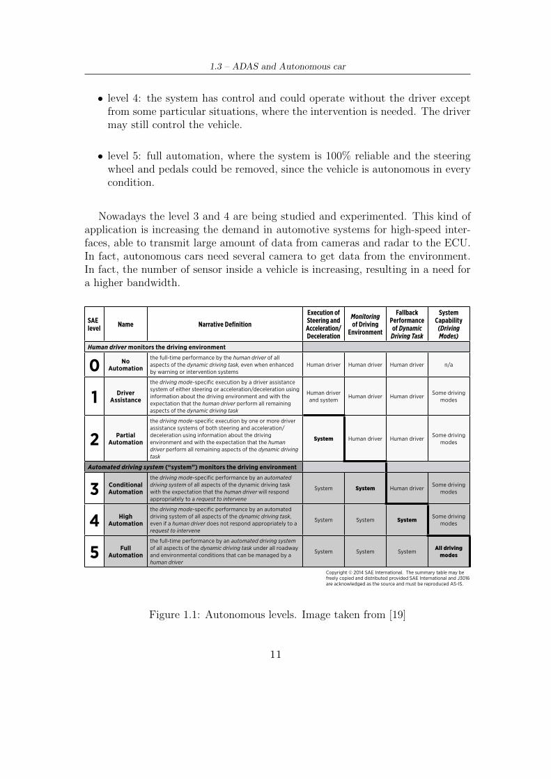
The Society of Automotive Engineers (SAE Internationl) has defined six levelsof automation of a systems. They go from 0, absence of any automation, to 5, thatis a completely reliable system in any driving circumstance that does not need thehuman assistance.
• level 0: the vehicle may inform the driver, but all actions are made by thehuman. In this category falls every assistance that warn the driver withouttaking any action.
• level 1: the system may perform some actions on the either the steering wheelor the brake. This is just an assistance and the driver is driving most of thetime. An example is the Adaptive Cruise Control, where the car manage thespeed while measuring the distance from the next vehicle.
• level 2: the system can maneuver the steering wheel and brakes in particularconditions, while the driver must be vigilant and monitor the environment.
• level 3: the system is able to operate reliably in certain conditions whilemonitoring the driving environment for possible dangers. The driver maybe noticed to take action within a certain time, but he does not have to befocused on the environment the whole time.
10
1.3 – ADAS and Autonomous car
• level 4: the system has control and could operate without the driver exceptfrom some particular situations, where the intervention is needed. The drivermay still control the vehicle.
• level 5: full automation, where the system is 100% reliable and the steeringwheel and pedals could be removed, since the vehicle is autonomous in everycondition.
Nowadays the level 3 and 4 are being studied and experimented. This kind ofapplication is increasing the demand in automotive systems for high-speed inter-faces, able to transmit large amount of data from cameras and radar to the ECU.In fact, autonomous cars need several camera to get data from the environment.In fact, the number of sensor inside a vehicle is increasing, resulting in a need fora higher bandwidth.
Figure 1.1: Autonomous levels. Image taken from [19]
11
1 – Introduction
1.4 Autodrive: European Project
Autodrive is a broad european project with the aim to gather companies anduniversities with the purpose to develop autonomous driving systems. It has thelong term goal to develop level 5 systems like an autonomous shuttle bus. In themiddle there are several shorter term goals that will bring to that final system.
The thesis work takes part of the project and its purpose is to design a develop-ing platform for another company part of the Autodrive project. The system willbe placed in a testing vehicle with all needed cameras and radars for the develop-ment of several kinds of ADAS systems. So it needs to interface with all sensors,be able to exchange a large quantity of data, process it and then safely take ac-tion. The system will be the base for developing algorithms and the applicationsoftware.
12
Chapter 2
Protocols and Standards
Here is presented a quick overview of the main standard interfaces present in theproject along with other standards. Because of the type of project, the main focuswill be on the physical layer of these interfaces.
2.1 SMARC
In the early stages of the design, the system has been chosen to be compliant withSMARC form factor standard. From the specification [23]:
SMARC (Smart Mobility Architecture) is a computer Module standardmaintained by the SGeT (Standardization Group for Embedded Tech-nologies). SMARC Modules are small form factor (82mm x 50mm and82mm x 80mm), low power (typically <6W) computer Modules that areused on a Carrier board that utilizes a 314 pin 0.5mm pitch right-anglememory socket style connector to host the Module
In other words, this defines a System on Module (SoM) which can act as a standalone PC, that can be inserted on a carrier board with the appropriate connector.The standard defines the dimensions of the PCB together with the interfaces tothe carrier board.
These modules can be bought and inserted on a application-specific board de-signed for the particular project. The standard allows interchangeability betweenmodules.
2.1.1 Specifications
The SGeT defines several aspects of the module. Some of them are completelymandatory, other are optional and model-dependent.
13
2 – Protocols and Standards
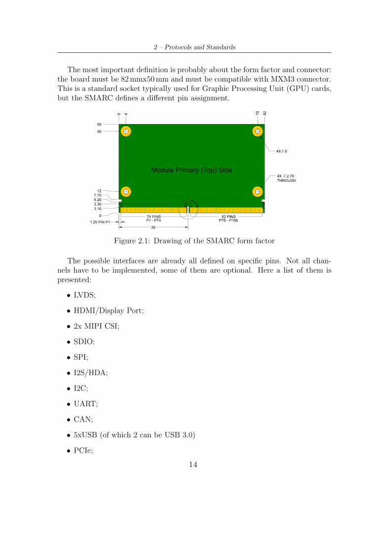
The most important definition is probably about the form factor and connector:the board must be 82mmx50mm and must be compatible with MXM3 connector.This is a standard socket typically used for Graphic Processing Unit (GPU) cards,but the SMARC defines a different pin assignment.
Figure 2.1: Drawing of the SMARC form factor
The possible interfaces are already all defined on specific pins. Not all chan-nels have to be implemented, some of them are optional. Here a list of them ispresented:
• LVDS;
• HDMI/Display Port;
• 2x MIPI CSI;
• SDIO;
• SPI;
• I2S/HDA;
• I2C;
• UART;
• CAN;
• 5xUSB (of which 2 can be USB 3.0)
• PCIe;
14
2.2 – PCIe
• Gigabit Ethernet;
• SATA.
It is not possible to assign a new purpose to unused pins, so they are left uncon-nected: violating the standard means to not guarantee compatibility. This is aquite complete set of the commonly used interface, including some high-speed onelike PCIe and Ethernet. The exact pin assignment can be read in the specificationdocument [23].
The communication between the module and the carrier along with the powerpass over the edge connector, which on the module side consists in only gold-platedcontacts directly on the PCB. The module is inserted in the socket parallel to thecarrier, resulting in a low-profile solution.
The power is delivered at a voltage between 3.0V and 5.25V, letting the moduleto regulate the power based on its own needs. The module should tolerate thewhole range, but it is allowed to be functional only in a subset of that range.
2.2 PCIe
PCI Express is an evolution of the old Peripheral Component Interconnect bus.It abandons the parallel structure in favor of a point-to-point high speed serialconnection. Its generality made it popular in a variety of fields such as consumer,server and industrial applications.
2.2.1 Structure
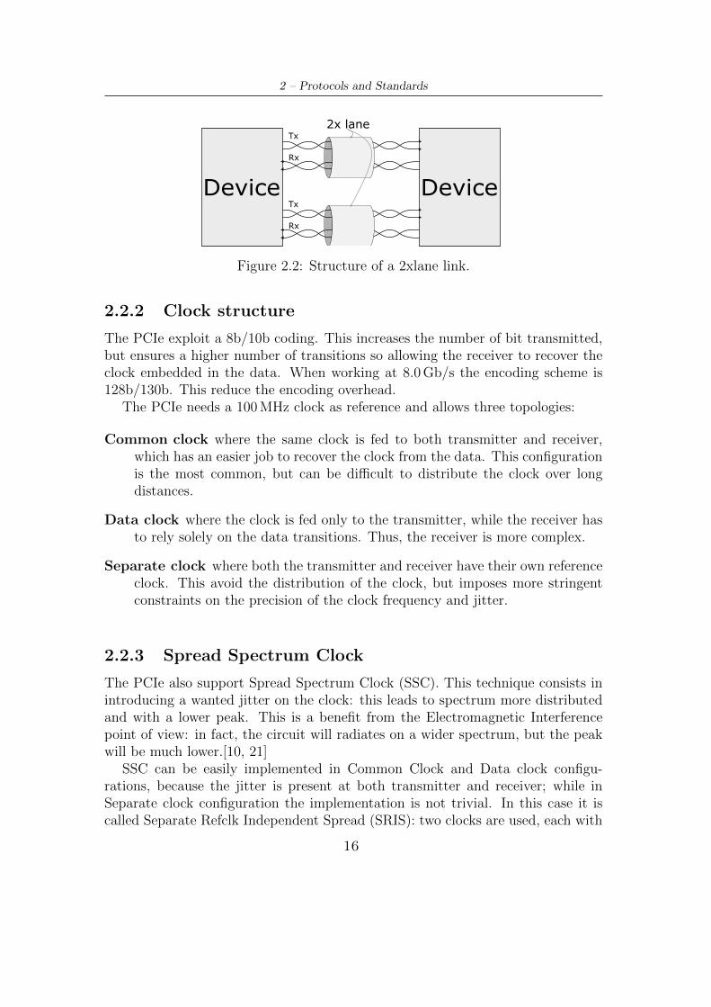
As already stated, the protocol consists in a point-to-point serial connection. Thisremoves the constraints and complexities about time arrival of single lines withinthe bus, also reducing the number of pins needed. The link may consist of multiplelanes, which is a couple of simplex differential pairs. Thanks to its low voltage lev-els, it reaches higher speeds while keeping a low power profile. If larger bandwidthis needed, more lanes can be used in a link.
A PCIe Switch can be used to split a link into multiple ones. The resultingnetwork is hierarchical, where the Root Complex is the node that communicateswith the central CPU and all other nodes are Endpoints.
On the software side PCIe is very similar to its predecessors PCI, in fact itmaintains software compatibility with it.
The lowest bit rate is 2.5Gb/s, while Generation 3.0 introduce 8.0Gb/s perlane. As already said, using multiple lanes largely increases the bandwidth.
15
2 – Protocols and Standards
Device Device
Rx
Tx2x lane
Rx
Tx
Figure 2.2: Structure of a 2xlane link.
2.2.2 Clock structure
The PCIe exploit a 8b/10b coding. This increases the number of bit transmitted,but ensures a higher number of transitions so allowing the receiver to recover theclock embedded in the data. When working at 8.0Gb/s the encoding scheme is128b/130b. This reduce the encoding overhead.
The PCIe needs a 100MHz clock as reference and allows three topologies:
Common clock where the same clock is fed to both transmitter and receiver,which has an easier job to recover the clock from the data. This configurationis the most common, but can be difficult to distribute the clock over longdistances.
Data clock where the clock is fed only to the transmitter, while the receiver hasto rely solely on the data transitions. Thus, the receiver is more complex.
Separate clock where both the transmitter and receiver have their own referenceclock. This avoid the distribution of the clock, but imposes more stringentconstraints on the precision of the clock frequency and jitter.
2.2.3 Spread Spectrum Clock
The PCIe also support Spread Spectrum Clock (SSC). This technique consists inintroducing a wanted jitter on the clock: this leads to spectrum more distributedand with a lower peak. This is a benefit from the Electromagnetic Interferencepoint of view: in fact, the circuit will radiates on a wider spectrum, but the peakwill be much lower.[10, 21]
SSC can be easily implemented in Common Clock and Data clock configu-rations, because the jitter is present at both transmitter and receiver; while inSeparate clock configuration the implementation is not trivial. In this case it iscalled Separate Refclk Independent Spread (SRIS): two clocks are used, each with
16
2.2 – PCIe
Common Clock Rx Architecture
PCIe LinkPCIe
Device A
100 MHz ±300ppm
PCIe Device B
Data Clocked Rx Architecture
100 MHz ±300ppm
PCIe LinkPCIe
Device APCIe
Device B
Separate Clock Architecture
PCIe LinkPCIe
Device APCIe
Device B
100 MHz ±300ppm
100 MHz ±300ppm
Figure 2.3: Three clock topologies of PCIe
Carrier Frequency
Reduced Amplitude and
EMI
Clock with SSC Off
Clock with SSC On
(downspread)
f
Figure 2.4: Spectral content of SSC
his own SSC. This further complicates the receiver, that should be able to recoverthat data despite the different frequencies.
2.2.4 Physical Layer
The serial nature of PCIe simplifies layout work: in fact, every lane can be berouted independently, without matching the length of all of them. Every lane isa pair with differential impedance of 100Ω. Capacitors must be placed in serieswith Tx lanes, in order to get an AC coupled signal. Another useful feature isthe Polarity inversion of the lines: it is possible to swap the two signals withina differential pair, thus avoiding vias during routing phase. Before starting com-munication, the PCIe controller perfrorm a link training, so configuring the linkwidth, the line polarity and performing lane-to-lane de-skew.
17
2 – Protocols and Standards
2.3 SATA
The SATA (Serial AT Attachment) interface is a bus used to interface a computerto a storage device. At the physical level is a point to point full duplex connection,with 100Ω differential lines. It needs AC coupling capacitors on signals. Theencoding is 8b/10b, that is 8 bits are mapped to 10 bits. Also in this case there isthe possibility to use Spread Spectrum Clock.
During power on, Out Of Band signaling is used to configure the link. In thissituation the differential line is not driven differentiallly but they are driven withthe same voltage.
2.4 USB
Universal Serial Bus is a well known interface used in consumer electronics for awide variety of applications, typically for PC-peripheral communication. It allowsto access multiple devices using hubs, creating a tiered-star topology: one singlehost connected to several hubs and devices. At most there can be 5 hubs betweenthe Host and the device, thus resulting in 7 tiers (where Tier 1 is the Host, Tier 7is the device).
2.4.1 Physical Layer
Up to version 3.0, the interface relied solely on a half-duplex differential pair(composed by signals often called D+ and D-). All communications are managedby the host computer, and only one device at a time can communicate.
It should have a differential impedance of 90Ω. The clock is embedded in thedata, featuring bit stuffing to ensure enough transitions. In the cable are alsocarried GND and a 5V VBUS, that can feed up to 500mA to the devices.
The 3.0 standard changed the number of wires, introducing two differentialpair, dedicated to transmitting and receiving thus reaching full-duplex operation(Tx+, Tx-, Rx+, Rx-). Since they are not directly retro-compatible with previousversions, inside the cable are also present older signals (D+ and D -) that are alsoused for configuration.
The several versions defines speed grades, shown in Tab. 2.1.
2.5 LPDDR4
Mobile devices has to cope with a trade-off between power savings and high per-formances. Together with the higher and higher media-orientation of new devices,there is the need for large, fast and low power memory. Because of that, JEDEC
18
2.5 – LPDDR4
Table 2.1: USB speeds
Name Speed [Mbit/s] Version
Half Speed 1.5 1.0Full Speed 12 1.0High Speed 480 2.0Super Speed 5000 3.0
has defined a new branch of memory standards in order to satisfy this demand:the Low Power Double Data Rate SDRAM.
It specifies a class of devices with standard performances, behavior and inter-face.
2.5.1 Architecture
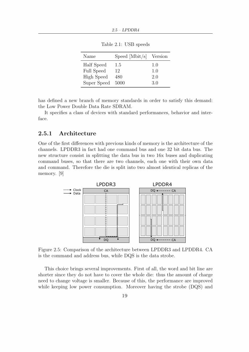
One of the first differences with previous kinds of memory is the architecture of thechannels. LPDDR3 in fact had one command bus and one 32 bit data bus. Thenew structure consist in splitting the data bus in two 16x buses and duplicatingcommand buses, so that there are two channels, each one with their own dataand command. Therefore the die is split into two almost identical replicas of thememory. [9]
CA
DQ
CADQ
CADQ
LPDDR3 LPDDR4ClockData
Figure 2.5: Comparison of the architecture between LPDDR3 and LPDDR4. CAis the command and address bus, while DQS is the data strobe.
This choice brings several improvements. First of all, the word and bit line areshorter since they do not have to cover the whole die: thus the amount of chargeneed to change voltage is smaller. Because of this, the performance are improvedwhile keeping low power consumption. Moreover having the strobe (DQS) and
19
2 – Protocols and Standards
clock pins on the same side reduces the power consuption: in fact, DQS is generatedstarting from the clock signal.
The two channels can be turned off independently, so giving the possibility tosave power if one of them is not used for long periods.
DMI signal (Data Mask inversion) was previously used only for data mask, butnow it has a double role.
Data mask is a useful feature to cope with the burst oriented nature of the device.It allows the controller to tell the RAM to discard some of the bytes sentduring the write burst. Writing not contiguous bytes create problem aboutparity bits used for Error Correction Code: they are calculated over the entirerange present in memory, including the bits not overwritten. In previousversion, this task was done by reading the range, modifying the wanted bits,recalculating the ECC and lastly writing the whole of it. In LPDDR4, thememory itself recalculate the new ECC even though some bytes have to beexcluded, thus saving transitions on bus.
Bus inversion allows to send an inverted replica of the data, and DMI signal isused to inform the receiver that the inversion has been made. If the numberof bits equal to 1 is greater than 4, the RAM or the controller will send theinverted data. This minimizes the number of 1s on the lines, thus reducingthe static power dissipated. In fact, the On Die Termination present on DQpins is connected to VSS, so current will flow through it only when the voltageis HIGH.
Like modern memories, this device features link training: it consists in a phasewhere the controller and the memory collaborates in order to find the optimalconfigurations for reference voltage, delays, signal strength and terminations. Anew feature regards the frequency set points. In fact, the LPDDR4 have a du-plicated set of configuration registers that can be used to store trained parameterof a higher frequency configuration. This allow to change configuration run-timewithout passing in an untrained state and possibly loosing the link. LPDDR4are designed for battery powered systems, so the possibility to switch between alow-power and a high-performance configuration is quite important.
2.6 HDMI
HDMI is a stanrdard interface used to send uncompressed video and audio datafrom a device to another. They are respectively called Source and Sink. Anexample is a PC as Source and a display as Sink.
At the core, it consists in 4 differential pair compliant with TMDS (TransitionMinimized Differential Signaling), but inside the cable there are also auxiliary
20
2.6 – HDMI
interfaces.
2.6.1 Architecture
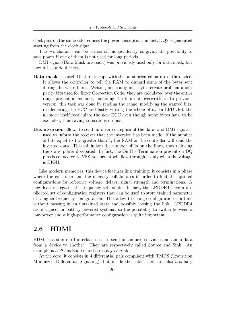
Among the secondary interfaces there is an I2C interface called DDC (Digital DataControl) used by the source to read configuration data from a ROM mounted onthe Sink. For instance, the memory stores the supported frequencies, resolutionsand data formats.
Another optional part of the interface is the Consumer Electronic Control(CEC), a one-wire bidirectional connection between devices. This allows the userto control through the remote all the devices connected with HDMI cables.
Video
Audio
Control/Status
TMDS Channel 0
TMDS Channel 1
TMDS Channel 2
TMDS Clock Channel
HDMIReceiver
Video
Audio
Control/Status
Display Data Channel (DDC)EDIDROM
CEC Line
HEAC
CEC CEC
HDMITransmitter
detect
Video
Audio
Control/Status
TMDS Channel 0
TMDS Channel 1
TMDS Channel 2
TMDS Clock Channel
HDMIReceiver
Video
Audio
Control/Status
Display Data Channel (DDC)EDIDROM
CEC LineCEC CEC
HDMITransmitter
High / Lowdetect
Figure 2.6: HDMI structure
The video and audio data is sent through the 4 differential pairs. One of themis used as pixel clock, providing a timing reference. During one pixel clock cycle,10 bits are sent on each one of the three remaining pairs, thus sending 30 bits. Assubsequently explained, data is actually encoded from 8 bits to 10, so the actualnumber of bits is 24.
The Source also provides a 5V power line, from which the Sink can absorb atmost 500mA.
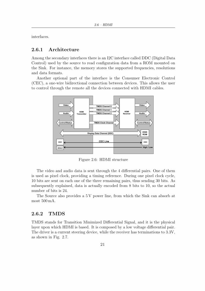
2.6.2 TMDS
TMDS stands for Transition Minimized Differential Signal, and it is the physicallayer upon which HDMI is based. It is composed by a low voltage differential pair.The driver is a current steering device, while the receiver has terminations to 3.3V,as shown in Fig. 2.7.
21
2 – Protocols and Standards
RTRT
AVcc
D D
Z0
Transmitter
ReceiverCurrentsource
Figure 2.7: TMDS architecture
The data is not sent as is, but it is encoded with a particular 8b/10b scheme(qis the encoded symbol, while D is the original byte):
• the LSB D[0] is not modified;
• the following fields is the result of the XOR or XNOR with the previous bit ofthat byte, in other words q[i] = D[i] XOR D[i− 1]. The operation is decidedin order to minimize transitions, and the 9th bit signals which operation hasbeen made;
• based on the previous bytes sent, the driver can decide to invert the wholesymbol q[0 : 8] and use q[9] to signal the inversion.
This type of encoding accomplishes two purposes: the first one is reducing thetotal number of transitions on the line, and it is done through the application ofXOR/XNOR functions. Less switching means less eletrco-magnetic radiation. Theother purpose is to try to balance the long term number of 1s and 0s sent, i.e. toreduce the running disparity. Through the inversion of the bus, the scheme ensurea low running disparity. Having signals with almost no DC component reduce theInter Symbolic Interference since, otherwise, during a long series of equal bits thelanes would get charged/discharged. [6]
2.6.3 Resolutions and frequencies
Depending on the link, several bit clocks are supported. This depends on bothSink and Source, as well as the cable used. Given a particular bandwidth, severalformats and resolutions can be supported.
There are several factors that affect the needed bandwidth. The first one isresolution: this is the total number of pixels that make up a frame of the video.The second one is the color depth: for each pixel the color is encoded into a fixed
22
2.7 – Ethernet
number of bits, that can vary from 24 to 36 bits. Moreover, the color scheme hasto be chosen: RGB ( Red, Green, Blue) and YCBCR (Luminance, Change of blue,Change of red) are supported. The last factor is the frame rate, that consists inhow many frames are sent every second.
So the total number of bits sent every second is:
resolution · colorDepth · frameRate
This workload is shared between the 3 data TMDS channels. For instance, witha resolution of 1280x720, a color depth of 24 bits and a frame rate of 30Hz, thetotal necessary bandwith is (1280 · 720) · 24 · 30 = 663MHz.
2.7 Ethernet
Ethernet is a collection of IEEE standards for Local Area Network. It definesseveral the lowest layers of the OSI (Open Model Interface) stack, from the Physicalto the Data Link layer.
2.7.1 Physical layers
The Ethernet can be transported over several kind of interconnections, from cop-per cables to optical fiber. The most common ones in consumer applications are10BASE-T, 100BASE-T and 1000BASE-T, where the first digits tell the overallspeed in Megabit/s. They are typically coupled with the RJ-45 standard plug.They all use 4 AC coupled twisted pair.
In the automotive sector 100BASE-T1 has become a popular solution. It cansend 100Mb/s over a single unshielded twisted pair. It keeps low costs while toler-ating harsh environment and coping with stringent Electromagnetic Compatibilityconstraints. It employs PAM3, that is three voltage levels are allowed. In automo-tive applications 100BASE-T1 can be used to deliver many kinds of data acrossthe vehicle.
2.7.2 MDI and MII
An Ethernet transceiver is composed by a MAC ( Medium Access Control) and aPHY (Physical Medium Transceiver). The first one is the controller that managethe second layer of the OSI stack so controlling the access to the shared medium,while the second one is the transceiver that translate the data to the right voltagelevels and the applying the needed encoding.
The two of them communicates with an 8 bit bi-directional bus called MII:Media Independent Interface. As the name says, it allows the exchange of databetween MAC and PHY regardless of the physical layer used.
23
2 – Protocols and Standards
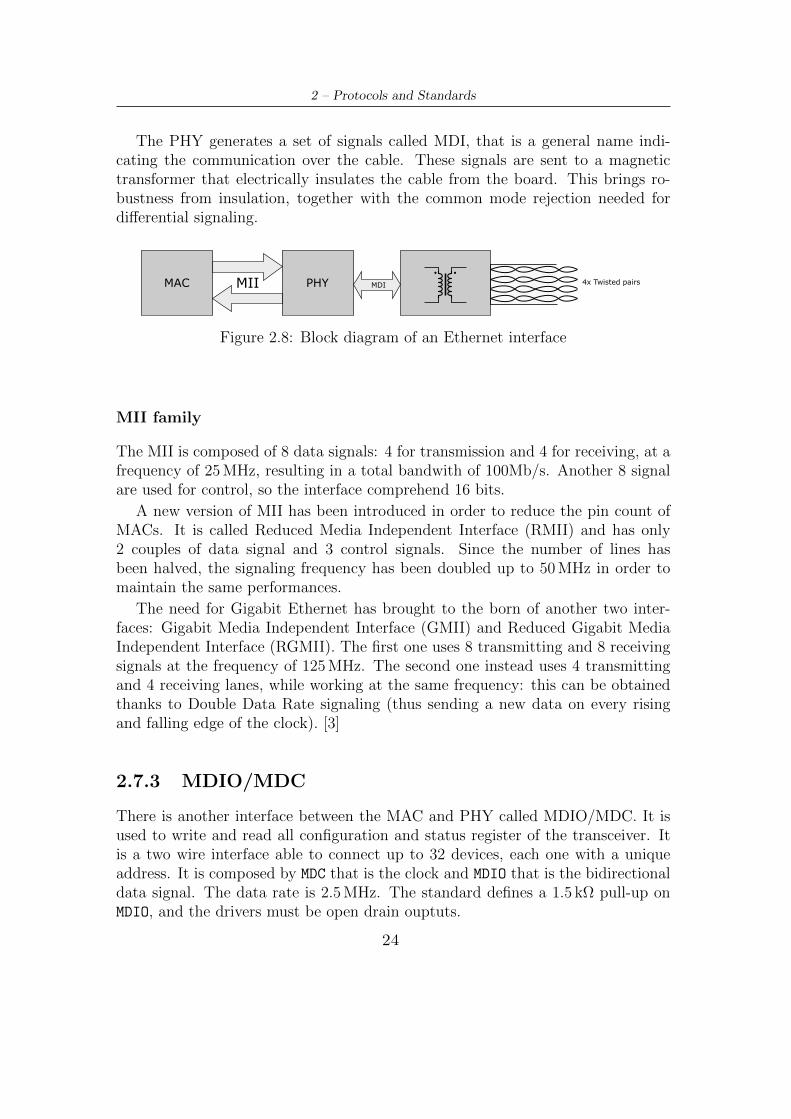
The PHY generates a set of signals called MDI, that is a general name indi-cating the communication over the cable. These signals are sent to a magnetictransformer that electrically insulates the cable from the board. This brings ro-bustness from insulation, together with the common mode rejection needed fordifferential signaling.
MAC PHY MDI 4x Twisted pairsMII
Figure 2.8: Block diagram of an Ethernet interface
MII family
The MII is composed of 8 data signals: 4 for transmission and 4 for receiving, at afrequency of 25MHz, resulting in a total bandwith of 100Mb/s. Another 8 signalare used for control, so the interface comprehend 16 bits.
A new version of MII has been introduced in order to reduce the pin count ofMACs. It is called Reduced Media Independent Interface (RMII) and has only2 couples of data signal and 3 control signals. Since the number of lines hasbeen halved, the signaling frequency has been doubled up to 50MHz in order tomaintain the same performances.
The need for Gigabit Ethernet has brought to the born of another two inter-faces: Gigabit Media Independent Interface (GMII) and Reduced Gigabit MediaIndependent Interface (RGMII). The first one uses 8 transmitting and 8 receivingsignals at the frequency of 125MHz. The second one instead uses 4 transmittingand 4 receiving lanes, while working at the same frequency: this can be obtainedthanks to Double Data Rate signaling (thus sending a new data on every risingand falling edge of the clock). [3]
2.7.3 MDIO/MDC
There is another interface between the MAC and PHY called MDIO/MDC. It isused to write and read all configuration and status register of the transceiver. Itis a two wire interface able to connect up to 32 devices, each one with a uniqueaddress. It is composed by MDC that is the clock and MDIO that is the bidirectionaldata signal. The data rate is 2.5MHz. The standard defines a 1.5 kΩ pull-up onMDIO, and the drivers must be open drain ouptuts.
24
2.8 – SD Card
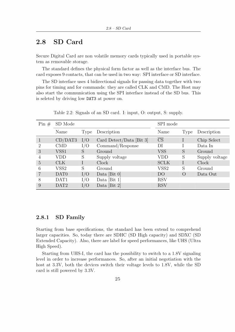
2.8 SD Card
Secure Digital Card are non volatile memory cards typically used in portable sys-tem as removable storage.
The standard defines the physical form factor as well as the interface bus. Thecard exposes 9 contacts, that can be used in two way: SPI interface or SD interface.
The SD interface uses 4 bidirectional signals for passing data together with twopins for timing and for commands: they are called CLK and CMD. The Host mayalso start the communication using the SPI interface instead of the SD bus. Thisis seleted by driving low DAT3 at power on.
Table 2.2: Signals of an SD card. I: input, O: output, S: supply.
Pin # SD Mode SPI mode
Name Type Description Name Type Description
1 CD/DAT3 I/O Card Detect/Data [Bit 3] CS I Chip Select2 CMD I/O Command/Response DI I Data In3 VSS1 S Ground VSS S Ground4 VDD S Supply voltage VDD S Supply voltage5 CLK I Clock SCLK I Clock6 VSS2 S Ground VSS2 S Ground7 DAT0 I/O Data [Bit 0] DO O Data Out8 DAT1 I/O Data [Bit 1] RSV9 DAT2 I/O Data [Bit 2] RSV
2.8.1 SD Family
Starting from base specifications, the standard has been extend to comprehendlarger capacities. So, today there are SDHC (SD High capacity) and SDXC (SDExtended Capacity). Also, there are label for speed performances, like UHS (UltraHigh Speed).
Starting from UHS-I, the card has the possibility to switch to a 1.8V signalinglevel in order to increase performances. So, after an initial negotiation with thehost at 3.3V, both the devices switch their voltage levels to 1.8V, while the SDcard is still powered by 3.3V.
25
2 – Protocols and Standards
Table 2.3: Capacity and speed of several versions
SD version Capacity
SDSC 128MB - 2GBSDHC 4GB - 32GBSDXC 64GB - 2TB
Speed Class Speed
Standard 25MB/sUHS-I 104MB/sUHS-II 312MB/s
2.9 MIPI CSI
The Camera Serial Interface is especially aided to the transmission of raw datafrom a camera to a microprocessor. It is maintained by Mobile Industry ProcessorInterface and has become quite popular in mobile systems. The communicationcan rely on several Physical layers also defined by MIPI, that differs on the topologyof the connection: the number of lines, the presence of clock signals and the typeof signal (single ended or differential).
Like for HDMI, for each pixel several bits have to be sent, depending on thecolor scheme. Also RAW data can be sent, before applying Bayer Filter. [1]
2.9.1 D-PHY
One of the most popular physical layer is the D-PHY. It relies on a scalable numberof differential lanes (1, 2 or 4). The data is source synchronous, meaning that onanother differential pair the clock is sent from the source. Since we are talkingabout a camera, the clock and the data are sent from the camera itself toward theprocessor.
One peculiar feature of this link is that it has two possible state: the first oneis the High-Speed state, where the lines are driven by differential drivers withan amplitude of 200mV. The other state is Low-Power, where instead the thedifferential pair is driven as two independent single ended signal, with a voltagelevel of 1.2V and they are not terminated. This state is used for control data sinceit can send only 10Mb/s, while the main data is sent in High-Speed state reachinga speed of 1Gb/s per line. Since in some case this physical layer could havebidirectional communication, a Contention Detector is used to detect collisionswhile sending data in low power state. [2]
2.9.2 MIPI DSI
The MIPI Alliance defines another standard called Display Serial Interface. Itserves the purpose of sending data from the processor to a display. While CSI and
26

2.10 – I2S
DSI may share the same physical layer, they differ in the protocol one, being twoindependent standards.
RX
Dp
Dn
TX
LP-TX
HS-RX
CD
RT
Data
Clock
Ctrl
Protocol Side
RTR T
Line Side
LP-RX
LP-CD
LaneControl
andInterface
Logic
HS-TX
contention Detector
Figure 2.9: D-PHY transceiver structure
2.10 I2S
The Inter-IC Sound bus is a serial bus interconnection intended for sending andreceiving audio data in a digital format. The basic mono-directional architectureis composed of 3 wires: the SCK is the bit-clock, WS stands for word select and SD
for serial data. The WS level indicates which audio channel is being transmitted:when low, the data is related to left channel; when high the data is related to rightchannel. The data is clocked by the SCK signal and it changes on the falling edge.
This bus is intended for always transmitting data at a constant rate, betweenintegrated circuits mounted on the same board. For instance, it can be used topass data from a codec to an audio Digital-Analog Converter.
SCK
WS
SD
WORD n–1RIGHT CHANNEL
WORD n+1RIGHT CHANNEL
WORD nLEFT CHANNEL
LSB MSBMSB
Figure 2.10: I2S timing diagram.
27

2 – Protocols and Standards
2.10.1 SAI and ESAI
The Synchronous Audio Interface is a peripheral of the iMX8 able to transmitaudio data in several formats and frames. Among the others, there is I2S. Thisperipherals has 6 total pins: 3 for transmitting data and 3 for receiving. The threesignals are SYNC (frame sync), BCLK (bit clock) and DAT (data). Those pins can bedriven in order to support I2S, where SYNC is connected to WS. Moreover, there isthe possibility to have receiver and transmitter working synchronously, i.e. usingonly one pair of control signals. This can be done if the input and output datahave the same sampling frequency.
The iMX8 also has two enhanced SAI : it basically a SAI but with six total datasignals. Those can be configured as both input and output.
28
Chapter 3
Components choice
This chapter focus is about the early design choices and a brief description of themost important components chosen is provided.
3.1 Requirement analysis
The Autodrive project require the development of a prototyping platform forADAS Systems. It must be able to acquire data from several cameras, be ableto communicate on a CAN network and it must have high-speed interfaces likeEthernet. The proposed structure is based on the separation of the system in tworegions: the first one should get and process the data, while the second one shouldbe the fail-safe part. This region is devoted to decision taking and should have ahigh safety level.
This work is focused on the data processing part. The iMX8 has been suggestedas microcontroller, due to his large number of interfaces, powerful cores and GPUtogether with its automotive grade.
Moreover, it has been chosen to design this part of the system like a separatephysical board. In the early stages of the project, it has been chosen to design aboard compliant with SMARC standard. The other board, devoted to safe decisionmaking, would host the SMARC module and has been design by another designerof the company Ideas&Motion.
Since a complete SMARC module based one the iMX8 would satisfy the re-quirement imposed, the new focus of the design has become the fulfillment of thestandard. In fact, many interfaces would probably be unused in the Autodriveproject, but they have been designed in order to get a complete System On Mod-ule. This is due to the whish of the company to get a module which could bereused in other projects with similar requirements.
In conclusion, the aim has been to fill as many interfaces of the SMARC module
29
3 – Components choice
as possible, trying to use as much as possible of the iMX8 peripherals.
3.2 iMX8 Processor
At the core of the project is the NXP processor called iMX8. It has various mul-timedia capabilities that along with automotive grade features makes it suitablefor infotainment applications. Beside that, it can also be used in industrial envi-ronment or in a single-board computer.[12, 14]
3.2.1 Overview
A general overview of the processor is given here:
• six ARM core architecture;
• two Graphical Processing Units (GPU) compatible with OpenGL library API;
• a Video Processing Unit (VPU) for video encoding and decoding;
• two controller for LPDDR4 SDRAM;
• SDIO 3.0 and eMMC 5.0 for storage interface;
• Quad-SPI;
• Display controller able to drive 1x4K or 4x Full HD displays;
• MIPI DSI, HDMI(Tx)/eDP and LVDS channel used to interface with displays;
• HDMI(Rx) and MIPI CSI in order to receive data from cameras;
• PCIe gen. 3.0;
• SATA 3.0;
• USB 3.0 and 2.0;
• two GigaBit Ethernet MAC RGMII;
• UART and I2C;
• SPDIF, SAI and ESAI for audio signals;
• CAN interfaces;
30
3.2 – iMX8 Processor
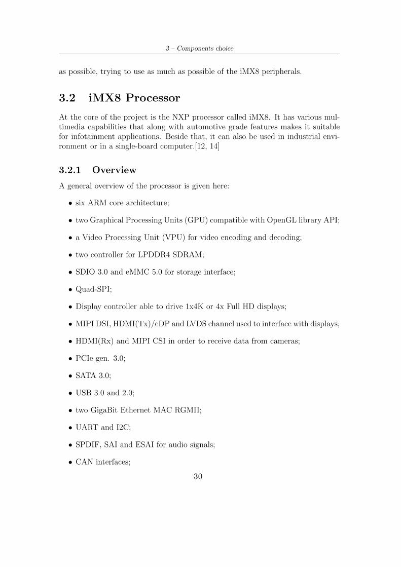
It is clear how the peripherals are mostly media-oriented. Also, many of theinterfaces includes high frequency signals ( greater than 1GHz).
Figure 3.1: Simplified block diagram taken from iMX8 datasheet [12]
31
3 – Components choice
3.2.2 ARM core
The processor is based on a multi-core architecture. All cores belongs to ARM-Cortex family. [13] In particular:
• 2x Cortex-A72 cores, used for compute-intensive tasks;
• 4x Cortex-A54 cores, used during low-power states;
• 2x Cortex-M4 cores, used to manage low-power general-purpose peripherals.
• a System Controller, providing an abstraction to the hardware peripherals,along with power and boot management.
These features allow the iMX8 to run a complete operating system, like Linux,Android or FreeRTOS.
Clusters
A set of homogeneous cores is called cluster. In this case there are two clusters:one composed by A72 and one by A54.
Each cluster can perform individual voltage and frequency scaling, while all theclusters can work together as a single multi-core processor. A L2 cache is sharedamong the cores in a cluster. Processes can be scheduled across cores of differenttypes.
Many other features are omitted, since they fall out of the scope of the thesis.
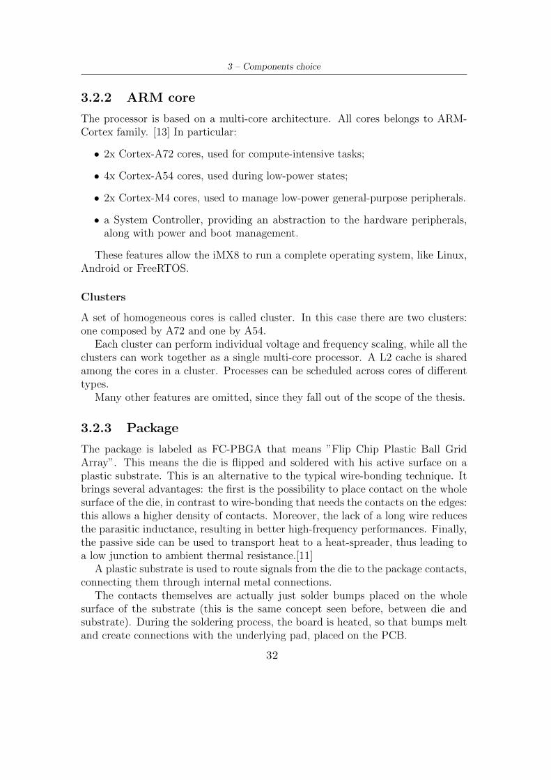
3.2.3 Package
The package is labeled as FC-PBGA that means ”Flip Chip Plastic Ball GridArray”. This means the die is flipped and soldered with his active surface on aplastic substrate. This is an alternative to the typical wire-bonding technique. Itbrings several advantages: the first is the possibility to place contact on the wholesurface of the die, in contrast to wire-bonding that needs the contacts on the edges:this allows a higher density of contacts. Moreover, the lack of a long wire reducesthe parasitic inductance, resulting in better high-frequency performances. Finally,the passive side can be used to transport heat to a heat-spreader, thus leading toa low junction to ambient thermal resistance.[11]
A plastic substrate is used to route signals from the die to the package contacts,connecting them through internal metal connections.
The contacts themselves are actually just solder bumps placed on the wholesurface of the substrate (this is the same concept seen before, between die andsubstrate). During the soldering process, the board is heated, so that bumps meltand create connections with the underlying pad, placed on the PCB.
32
3.3 – USB Hub
Underfill
Flip Chip Solder Bump
CapacitorLid / Heat SpreaderThermal Interface Material
Package SubstrateBGA Solder Ball
Lid Adhesive
Silicon Die
Figure 3.2: Section of FCPBGA. Image taken from NXP document.[11]
Collapsing and non collapsing connections
The contact between the bump and the pad can be classified into two groups.
The first one, called non collapsing, is the result of a Solder Mask Defined Pad,where the metal pad is larger than the soldermask opening. In this case the solderis touching only the top surface.
In the second case, the solder can create a bonding also with the side of themetal pad, since the solder mask opening is larger than the pad (non Solder MaskDefined). A section of the two can be seen in Fig. 3.3.
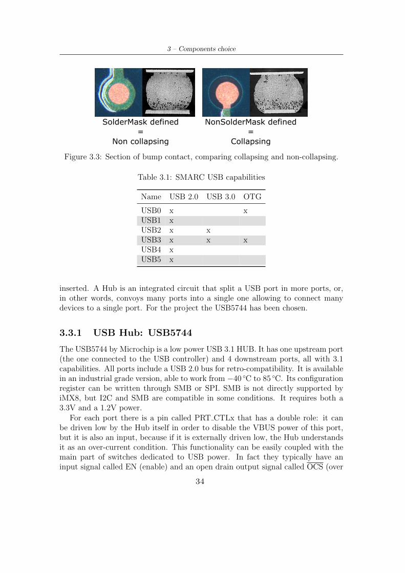
These two types have some pros and cons. The collapsing contact is typicallyused with pin pitch greater or equal to 0.65mm and bring a larger contact areawith the pad. Moreover, there is more space to route line between pads. On theother hand, tests show that this type of contact are mechanically weaker thanthe other type: in fact, the copper pad may detach from the substrate in caseof shock. The non-collapsing contact instead has less contact area, while it ismore mechanically robust since the solder mask overlap increases the pad adhesionto the PCB. This type is suitable for component with smaller pin-pitch where viain pad may be needed: in fact the larger copper area can suit more easily the via.
3.3 USB Hub
The iMX8 has one USB 2.0 OTG interface and a USB 3.0 interface (which com-prehends also a 2.0 bus); it also has another 2.0 controller connected to a HSIC(High Speed Inter Chip) interface: a single low voltage differential line intendedfor on-board communication. The SMARC module instead has 6 interfaces, twoof which that are capable of 3.0 operations.
In order to have as many buses as possible, a USB Hub has been chosen to be
33
3 – Components choice
SolderMask defined=
Non collapsing
NonSolderMask defined=
Collapsing
Figure 3.3: Section of bump contact, comparing collapsing and non-collapsing.
Table 3.1: SMARC USB capabilities
Name USB 2.0 USB 3.0 OTG
USB0 x xUSB1 xUSB2 x xUSB3 x x xUSB4 xUSB5 x
inserted. A Hub is an integrated circuit that split a USB port in more ports, or,in other words, convoys many ports into a single one allowing to connect manydevices to a single port. For the project the USB5744 has been chosen.
3.3.1 USB Hub: USB5744
The USB5744 by Microchip is a low power USB 3.1 HUB. It has one upstream port(the one connected to the USB controller) and 4 downstream ports, all with 3.1capabilities. All ports include a USB 2.0 bus for retro-compatibility. It is availablein an industrial grade version, able to work from −40 C to 85 C. Its configurationregister can be written through SMB or SPI. SMB is not directly supported byiMX8, but I2C and SMB are compatible in some conditions. It requires both a3.3V and a 1.2V power.
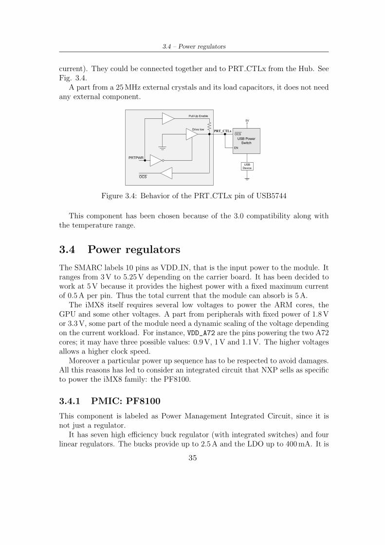
For each port there is a pin called PRT CTLx that has a double role: it canbe driven low by the Hub itself in order to disable the VBUS power of this port,but it is also an input, because if it is externally driven low, the Hub understandsit as an over-current condition. This functionality can be easily coupled with themain part of switches dedicated to USB power. In fact they typically have aninput signal called EN (enable) and an open drain output signal called OCS (over
34
3.4 – Power regulators
current). They could be connected together and to PRT CTLx from the Hub. SeeFig. 3.4.
A part from a 25MHz external crystals and its load capacitors, it does not needany external component.
USB Power Switch
PRTPWR
EN
OCS
OCS
Pull-Up Enable
5V
USB Device
PRT_CTLxDrive low
Figure 3.4: Behavior of the PRT CTLx pin of USB5744
This component has been chosen because of the 3.0 compatibility along withthe temperature range.
3.4 Power regulators
The SMARC labels 10 pins as VDD IN, that is the input power to the module. Itranges from 3V to 5.25V depending on the carrier board. It has been decided towork at 5V because it provides the highest power with a fixed maximum currentof 0.5A per pin. Thus the total current that the module can absorb is 5A.
The iMX8 itself requires several low voltages to power the ARM cores, theGPU and some other voltages. A part from peripherals with fixed power of 1.8Vor 3.3V, some part of the module need a dynamic scaling of the voltage dependingon the current workload. For instance, VDD_A72 are the pins powering the two A72cores; it may have three possible values: 0.9V, 1V and 1.1V. The higher voltagesallows a higher clock speed.
Moreover a particular power up sequence has to be respected to avoid damages.All this reasons has led to consider an integrated circuit that NXP sells as specificto power the iMX8 family: the PF8100.
3.4.1 PMIC: PF8100
This component is labeled as Power Management Integrated Circuit, since it isnot just a regulator.
It has seven high efficiency buck regulator (with integrated switches) and fourlinear regulators. The bucks provide up to 2.5A and the LDO up to 400mA. It is
35
3 – Components choice
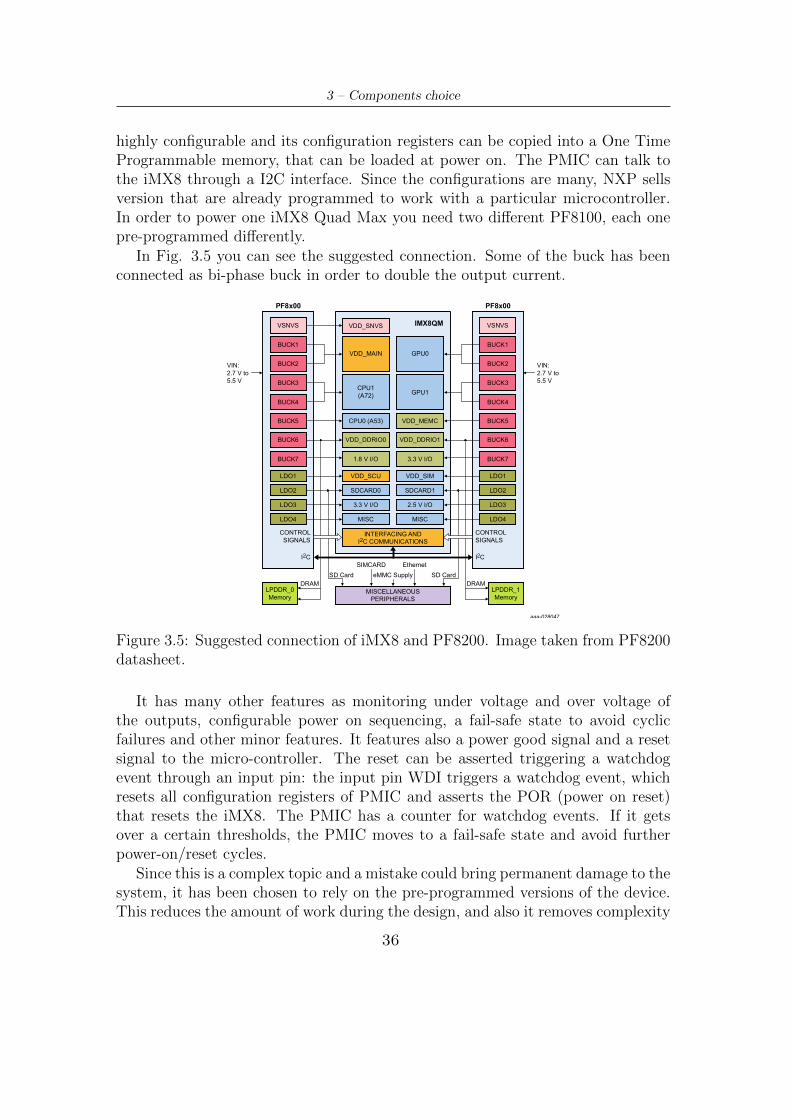
highly configurable and its configuration registers can be copied into a One TimeProgrammable memory, that can be loaded at power on. The PMIC can talk tothe iMX8 through a I2C interface. Since the configurations are many, NXP sellsversion that are already programmed to work with a particular microcontroller.In order to power one iMX8 Quad Max you need two different PF8100, each onepre-programmed differently.
In Fig. 3.5 you can see the suggested connection. Some of the buck has beenconnected as bi-phase buck in order to double the output current.
aaa-028047
IMX8QM
PF8x00
VDD_SNVS
VDD_MAIN
CPU1(A72)
CPU0 (A53)
VDD_DDRIO0
1.8 V I/O
VDD_SCU
SDCARD0
3.3 V I/O
MISC
GPU1
GPU0
VDD_MEMC
VDD_DDRIO1
3.3 V I/O
VSNVS
BUCK7
BUCK6
BUCK5
BUCK4
BUCK3
BUCK2 VIN:2.7 V to5.5 V
VIN:2.7 V to5.5 V
BUCK1
VDD_SIM
SDCARD1
2.5 V I/O
MISC
LDO1
LDO2
LDO3
LDO4
PF8x00
VSNVS
BUCK7
BUCK6
BUCK5
BUCK4
BUCK3
BUCK2
BUCK1
LDO1
LDO2
LDO3
LDO4
INTERFACING ANDI2C COMMUNICATIONS
CONTROLSIGNALS
I2C
DRAMSD Card
Ethernet
eMMC Supply
SIMCARD
SD CardDRAM
CONTROLSIGNALS
I2C
LPDDR_0Memory
LPDDR_1Memory
MISCELLANEOUSPERIPHERALS
Figure 3.5: Suggested connection of iMX8 and PF8200. Image taken from PF8200datasheet.
It has many other features as monitoring under voltage and over voltage ofthe outputs, configurable power on sequencing, a fail-safe state to avoid cyclicfailures and other minor features. It features also a power good signal and a resetsignal to the micro-controller. The reset can be asserted triggering a watchdogevent through an input pin: the input pin WDI triggers a watchdog event, whichresets all configuration registers of PMIC and asserts the POR (power on reset)that resets the iMX8. The PMIC has a counter for watchdog events. If it getsover a certain thresholds, the PMIC moves to a fail-safe state and avoid furtherpower-on/reset cycles.
Since this is a complex topic and a mistake could bring permanent damage to thesystem, it has been chosen to rely on the pre-programmed versions of the device.This reduces the amount of work during the design, and also it removes complexity
36
3.5 – Ethernet
from the board, because the OTP memory does not need to be programmed onboard.
This device can be sold with code PF8200 which has a ASIL B safety level: thismeans that is safer with respect to failures; in fact it has an improved capabilityof self-testing.
3.5 Ethernet
The iMX8 Quad Max include 2 Gigabit Ethernet MACs with a RGMII interface.The SMARC standard requires to pass on the connector the MDI signals (the onegenerated by the PHY), and it provides two Ethernet interfaces.
It is clear that PHYs IC are needed on the module, in order to translate RGMIIto MDI. It must be compatible with GigaBit Ethernet and must have RGMIIinterface.
3.5.1 PHY: KSZ9031RNX
Amongst the commercial products, the KSZ9031RNX has been chosen. It providesthe required speed and RGMII interface, supporting 10BASE-T,100BASE-T and1000BASE-T. It is manufactured by Microchip which also offers an automotivealternative version of the chip. It has a 7x7mm QFN package with 48 pins and anexposed pad for thermal dissipation.
It needs both 3.3V and 1.2V to be powered. It provides a pin that can beconnected to the gate of an external PMOS in order to form an LDO to regulate1.2V from 3.3V. Also, an external crystal is needed for 25MHz clock. On theother hand, termination resistor for the MDI differential pairs are embedded onthe die.
Several strapping pins are present in order to set the MDIO address, enable allor part of its capabilities and set the LED pins behavior. Strapping pins are readat power on: the PHY detects if there are pull up or pull down resistor connected;after that, the pins are used as normal with their original function.
3.6 Main memory
The iMX8 has two memory controller to communicate with external RAM throughDDR4 or LPDDR4. On an evaluation board of the iMX8 by NXP, two of the samekind of LPDDR4 memory were used, with a capacity of 3GB each. The certaintythat this component is compatible with the iMX8, together with the possibilityto buy an automotive version of the memory, has lead to the choice of using
37
3 – Components choice
this component. A total capacity 6GB should be enough for a wide spectrum ofapplications.
3.6.1 LPDDR4: MT53B768M32D4
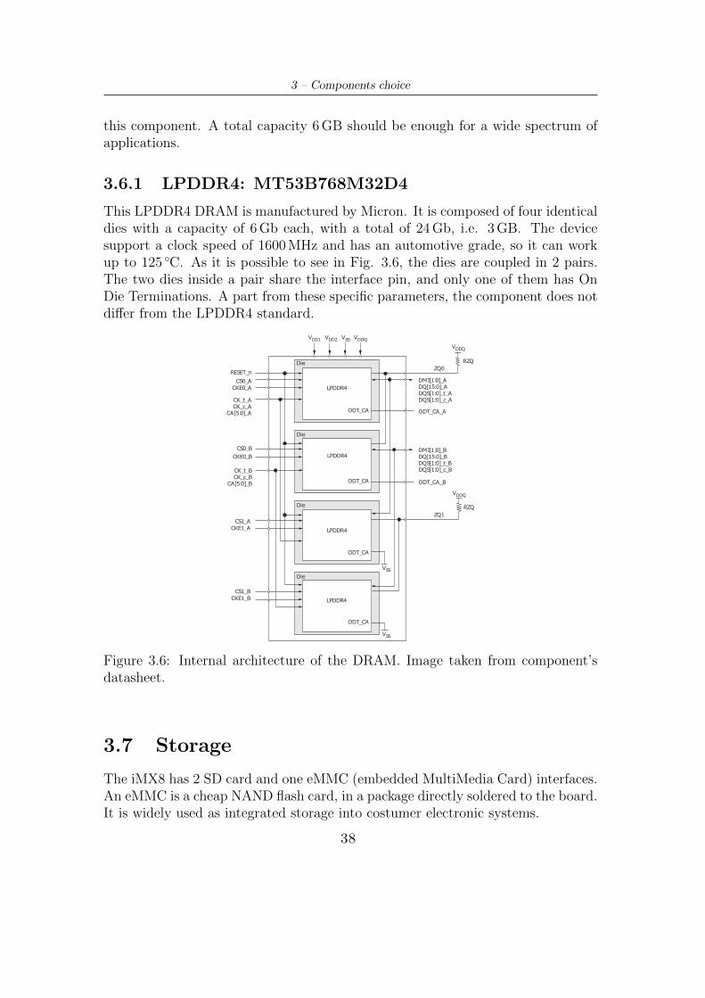
This LPDDR4 DRAM is manufactured by Micron. It is composed of four identicaldies with a capacity of 6Gb each, with a total of 24Gb, i.e. 3GB. The devicesupport a clock speed of 1600MHz and has an automotive grade, so it can workup to 125 C. As it is possible to see in Fig. 3.6, the dies are coupled in 2 pairs.The two dies inside a pair share the interface pin, and only one of them has OnDie Terminations. A part from these specific parameters, the component does notdiffer from the LPDDR4 standard.
LPDDR4
Die
RESET_n
CS0_BCKE0_B
CKE0_ACS0_A
CK_t_BCK_c_B
CA[5:0]_B
CK_t_ACK_c_A
CA[5:0]_A
DMI[1:0]_BDQ[15:0]_BDQS[1:0]_t_BDQS[1:0]_c_B
DMI[1:0]_ADQ[15:0]_ADQS[1:0]_t_ADQS[1:0]_c_A
ODT_CA_A
Die
Die
CS1_BCKE1_B
CKE1_ACS1_A
ODT_CA_B
LPDDR4
Die
VDD1 VDD2 VSS VDDQ
ZQ0RZQ
VDDQ
RZQ
VDDQ
ZQ1
LPDDR4
LPDDR4
ODT_CA
ODT_CA
ODT_CA
ODT_CA
VSS
VSS
Figure 3.6: Internal architecture of the DRAM. Image taken from component’sdatasheet.
3.7 Storage
The iMX8 has 2 SD card and one eMMC (embedded MultiMedia Card) interfaces.An eMMC is a cheap NAND flash card, in a package directly soldered to the board.It is widely used as integrated storage into costumer electronic systems.
38

3.8 – NOR Flash: MT35XU512ABA
3.7.1 eMMC: MTFC32GAK
This is a 5.0 eMMC compatible card that can be powered at 3.3V. It has a capacityof 32GB. It is packaged in three version of BGA: 100 balls, 153 balls and 169 balls.The eMMC interface consists in a 8 bit bi-directional data lines. In addition thereare CLK and CMD pins used for control and commands. Commands are sentserially on CMD from Host to device, as well as the response from device to Host.The data instead can be sent in both direction on DAT0-DAT7. Multiple blockcan be read or written in a burst, as Fig. 3.8. The interface is very similar to theSD one, but it has 8 bit interface.
Fromhost tocard(s)
CMD
DAT
Command
Data fromcard to host
Command Response
Fromcard to
host
Block read operation
Multiple block read operation
Response
Data stop operation
Data block crc Data block crcData block crc
Stop commandstops data transfer
Figure 3.7: Behavior of a eMMC bus. Image taken from JEDEC specifications.[8]
There are two possible speed states: HS200 and HS400. In the first one, one bitper each line is sent at every CLK cycle. The clock has a frequency of 200MHz,resulting in 200MB/s. The HS400 singaling instead adopts Double Data Rate, sowhile keeping 200MHz clock, it reaches 400MB/s. In this state, a Strobe is sentfrom the device to the host, easing the Host sampling of received data.
3.8 NOR Flash: MT35XU512ABA
The iMX8 can also boot from a NOR Flash with an SPI interface, with a capacityof 512 Mb. The chosen device is a Micron product. It can be interfaced both withoctal SPI (8 half-duplex lines) and DDR SPI. It must be powered at 1.8V.
3.9 PCIe Clock
As already seen in Section 2.2.1, an important part of the PCIe is the clock gen-eration and distribution. Every PCIe link needs a reference clock of 100MHz; inaddition, the Root complex ( i.e. the iMX8) also needs a reference clock. Thisclock is switching at a frequency high enough to have the need to avoid stubs andimpedance mismatches: thus it is a bad idea connecting several devices to the sameclock. Because of this, three clock signals are needed (2 links, 1 root complex).
Many PCIe specific clock generators have multiple outputs in order to satisfythis kind of needs.
39
3 – Components choice
Two possible components are considered, and later the second one has beenchosen.
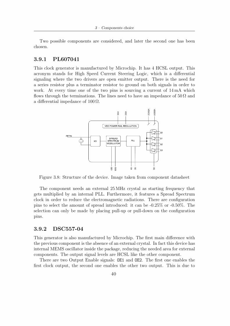
3.9.1 PL607041
This clock generator is manufactured by Microchip. It has 4 HCSL output. Thisacronym stands for High Speed Current Steering Logic, which is a differentialsignaling where the two drivers are open emitter output. There is the need fora series resistor plus a terminator resistor to ground on both signals in order towork. At every time one of the two pins is sourcing a current of 14mA whichflows through the terminations. The lines need to have an impedance of 50Ω anda differential impedance of 100Ω.
Figure 3.8: Structure of the device. Image taken from component datasheet
The component needs an external 25MHz crystal as starting frequency thatgets multiplied by an internal PLL. Furthermore, it features a Spread Spectrumclock in order to reduce the electromagnetic radiations. There are configurationpins to select the amount of spread introduced: it can be -0.25% or -0.50%. Theselection can only be made by placing pull-up or pull-down on the configurationpins.
3.9.2 DSC557-04
This generator is also manufactured by Microchip. The first main difference withthe previous component is the absence of an external crystal. In fact this device hasinternal MEMS oscillator inside the package, reducing the needed area for externalcomponents. The output signal levels are HCSL like the other component.
There are two Output Enable signals: OE1 and OE2. The first one enables thefirst clock output, the second one enables the other two output. This is due to
40
3.10 – Wireless communication: ATWILC3000
the fact that CLK1 and CLK2 are derived from the same oscillator and they aresynchronous: so one pin turns them off at the same time.
This component has been chosen because it has the exact number of neededoutput, as well as having a reduced total footprint due to the absence of an externalcrystal. Moreover, having two OE pins, there is the possibility to disable theoutputs in a finer way, thus saving more power.
The only drawback of this component is the absence of the Spread SpectrumClocks. Since SSC is an aid to be compliant during Electro-Magnetic Emissiontests, the hosting company decided to try this first version of the board withoutit.
3.10 Wireless communication: ATWILC3000
Since it does not complicate the project and it does provides useful features, anATWILC3000 module has been added. This module provides a Bluetooth 4.0and a WiFi IEEE 802.11 b/g/n interfaces. The antennas are embedded on themodule, so no additional components are needed. It can be powered at both 1.8Vand 3.3V.
The WiFi module can communicate through a SPI or SDIO interface. Insteadthe Bluetooth submodule interface with a UART with handshake signals (ClearTo Send, Request To Send).
3.11 Auxiliary connector
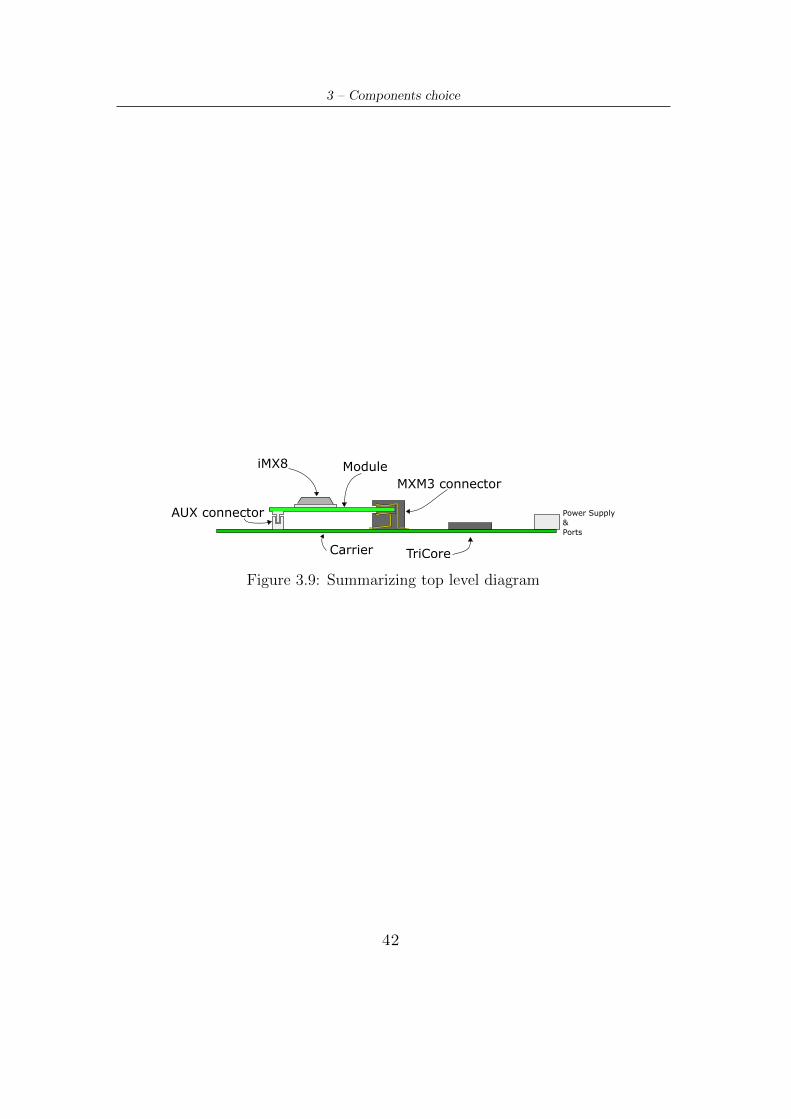
Not all interfaces of the iMX8 can pass on the SMARC-defined connector. In orderto avoid waste of resources, an additional connector has been added on the bottomside of the module. It has been chosen in order to have a mating height (the heightwhen female and male are matched) equal to the height of the MXM3 connectorwhere the module is inserted. In this way, if the male connector is present on thecarrier at the right height, both connector will match during insertion.
This connector belongs to the FX8C by Hirose. The interfaces passing on thiscustom connector, i.e. not defined by SGET, are the least important: the modulehas an already complete set of features when only the standard SMARC connectoris used.
41
3 – Components choice
MXM3 connector
AUX connector
Carrier
Module
Power Supply&Ports
iMX8
TriCore
Figure 3.9: Summarizing top level diagram
42
Chapter 4
Module Architecture
A high-level description of the final structure of the system is here provided. Theexplanation is aided by blocks diagram illustrating the general concept.
4.1 Top level
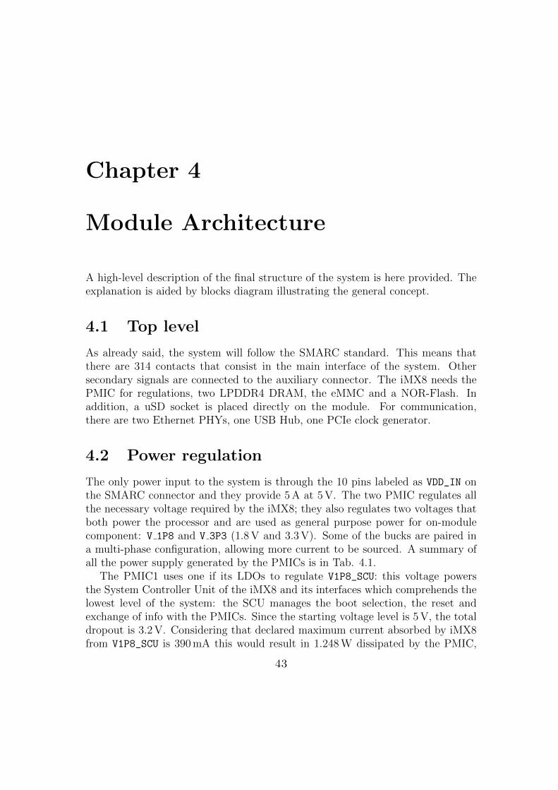
As already said, the system will follow the SMARC standard. This means thatthere are 314 contacts that consist in the main interface of the system. Othersecondary signals are connected to the auxiliary connector. The iMX8 needs thePMIC for regulations, two LPDDR4 DRAM, the eMMC and a NOR-Flash. Inaddition, a uSD socket is placed directly on the module. For communication,there are two Ethernet PHYs, one USB Hub, one PCIe clock generator.
4.2 Power regulation
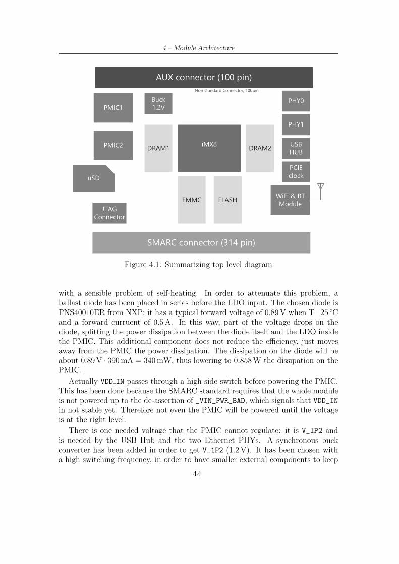
The only power input to the system is through the 10 pins labeled as VDD_IN onthe SMARC connector and they provide 5A at 5V. The two PMIC regulates allthe necessary voltage required by the iMX8; they also regulates two voltages thatboth power the processor and are used as general purpose power for on-modulecomponent: V 1P8 and V 3P3 (1.8V and 3.3V). Some of the bucks are paired ina multi-phase configuration, allowing more current to be sourced. A summary ofall the power supply generated by the PMICs is in Tab. 4.1.
The PMIC1 uses one if its LDOs to regulate V1P8_SCU: this voltage powersthe System Controller Unit of the iMX8 and its interfaces which comprehends thelowest level of the system: the SCU manages the boot selection, the reset andexchange of info with the PMICs. Since the starting voltage level is 5V, the totaldropout is 3.2V. Considering that declared maximum current absorbed by iMX8from V1P8_SCU is 390mA this would result in 1.248W dissipated by the PMIC,
43
4 – Module Architecture
iMX8
PMIC1
PMIC2
Buck 1.2V
PHY0
PHY1
USB HUBDRAM1 DRAM2
EMMC FLASH
PCIE clockuSD
SMARC connector (314 pin)
AUX connector (100 pin)
JTAGConnector
Non standard Connector, 100pin
WiFi & BT Module
Figure 4.1: Summarizing top level diagram
with a sensible problem of self-heating. In order to attenuate this problem, aballast diode has been placed in series before the LDO input. The chosen diode isPNS40010ER from NXP: it has a typical forward voltage of 0.89V when T=25 Cand a forward curruent of 0.5A. In this way, part of the voltage drops on thediode, splitting the power dissipation between the diode itself and the LDO insidethe PMIC. This additional component does not reduce the efficiency, just movesaway from the PMIC the power dissipation. The dissipation on the diode will beabout 0.89V · 390mA = 340mW, thus lowering to 0.858W the dissipation on thePMIC.
Actually VDD IN passes through a high side switch before powering the PMIC.This has been done because the SMARC standard requires that the whole moduleis not powered up to the de-assertion of _VIN_PWR_BAD, which signals that VDD_INin not stable yet. Therefore not even the PMIC will be powered until the voltageis at the right level.
There is one needed voltage that the PMIC cannot regulate: it is V_1P2 andis needed by the USB Hub and the two Ethernet PHYs. A synchronous buckconverter has been added in order to get V_1P2 (1.2V). It has been chosen witha high switching frequency, in order to have smaller external components to keep
44
4.2 – Power regulation
Table 4.1: Regulator assignement to power supply names.
PMIC number RegulatorPower Supplyname
Voltage range [V] Output current [A]
1 SW11 SW2
V MAIN 0.95 - 1.10 5
1 SW31 SW4
V CPU1 0.85 - 1.15 5
1 SW5 V CPU0 0.85 - 1.15 2.51 SW6 V DDRIO0 1.06 - 1.17 2.51 SW7 V 1P8 1.8 2.51 LDO1 V1P8 SCU 1.8 0.41 LDO2 V SD1 1.8 / 3.3 0.41 LDO3 - - -1 LDO4 - - -2 SW12 SW2
V GPU0 0.95 1.10 5
2 SW32 SW4
V GPU1 0.95 - 1.10 5
2 SW5 V MEMC 1.05 - 1.15 2.52 SW6 V DDRIO1 1.06 - 1.17 2.52 SW7 V 3P 3.3 2.52 LDO1 - - -2 LDO2 V SD2 1.8 / 3.3 0.42 LDO3 - - -2 LDO4 - - -
a low total footprint. The chosen converter is TPS6206 from Texas Instrument.It is an automotive regulator with a switching frequency of 3MHz and an outputcurrent of 2A. It is able to move to a power-save state when the load is reduced:it decreases the switching frequency and passes from Pulse Width Modulation toPulse Frequency Modulation. The purpose is to reduce the quiescent current tokeep a high efficiency.
4.2.1 Coin cell or SuperCapacitor
The SMARC defines a pin dedicated to be connected on the Carrier to a LithiumCell or a super capacitor, with the function of a backup power for keeping the timewhen the system is powered off. The PMIC has a particular regulator connected tothe SNVS region of the iMX8, which is the part that manages the RTC; moreover
45
4 – Module Architecture
the PMIC itself can also charge up the coin cell or the SuperCapacitor from thesame input pin when the main power is on. Since they have compatible features,they have been connected together. In this way, the coin cell on the carrier powersthe SNVS whenever the main power is off; instead when VDD_IN is present, currentflows from the PMIC toward the cell in order to charge it.
4.3 Boot sequence
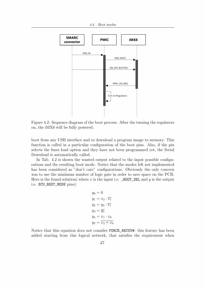
When power is provided to the module, several events take place.
• First of all, VDD_IN powers the PMIC.
• The PMIC is connected in such a way that it is not enabled as soon as theinput voltage is present. Instead it waits for its pin PWRON pin to read ahigh voltage. So all its output are disabled, except for VSNVS that is alwaysenabled.
• The pin VSNVS is connected to VDD_SNVS of the iMX8 which powers a smallpart of the iMX8. This block contains ON_OFF_BUTTON and PMIC_ON_REQ.The first one is connected through a dedicated SMARC pin to a button onthe carrier.
• When the button on the carrier is pressed, the signal arrives to the iMX8.Then, it asserts PMIC_ON_REQ so requesting the PMIC to turn on.
• At that point, the PMIC finally turns on all its regulators thus powering theiMX8.
4.4 Boot modes
Upon the release of _POR the System Controller Unit of the iMX8 reads a set ofpins in order to decided from which peripherals it should load the program image.
The SMARC specifications defines 3 pins of the connector for boot selections,performed through switches on the carrier. For each of the 8 combination thereis a boot source, that can be PCIe, USB, SD etc. Some of this can be left notimplemented. The iMX8 instead has 6 bits for selecting the boot source withtotally different value. This means that a simple logic net is needed to translateSMARC values to the one understandable by the iMX8.
In addition to that, a FORCE_RECOV# pin is routed through the SMARC con-nector. The standard says that it is driven low by the carrier in order to overwritepart of the boot code, reading from a USB device connected to USB0. This re-quirement can be satisfied by the USB Serial Download of the iMX8. It allow to
46
4.4 – Boot modes
SMARCconnectorSMARCconnector PMICPMIC iMX8iMX8
VDD_IN
VDD_SNVS
ON_OFF_BUTTON
PMIC_ON_REQ
Turn on Regulators
Figure 4.2: Sequence diagram of the boot process. After the turning the regulatorson, the iMX8 will be fully powered.
boot from any USB interface and to download a program image to memory. Thisfunction is called in a particular configuration of the boot pins. Also, if the pinselects the fuses load option and they have not been programmed yet, the SerialDownload is automatically called.
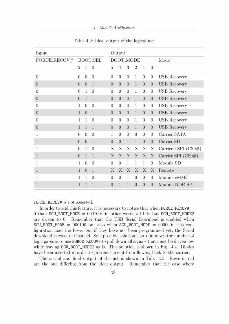
In Tab. 4.2 is shown the wanted output related to the input possible configu-rations and the resulting boot mode. Notice that the modes left not implementedhas been considered as ”don’t care” configurations. Obviously the only concernwas to use the minimum number of logic gate in order to save space on the PCB.Here is the found solution( where x is the input i.e. _BOOT_SEL and y is the outputi.e. SCU_BOOT_MODE pins):
y0 = 0
y1 = x2 · x1
y2 = y3 · x1
y3 = y5
y4 = x1 · x0
y5 = x2 + x0
Notice that this equation does not consider FORCE_RECOV#: this feature has beenadded starting from this logical network, that satisfies the requirement when
47
4 – Module Architecture
Table 4.2: Ideal output of the logical net
Input Output
FORCE RECOV# BOOT SEL BOOT MODE Mode
2 1 0 5 4 3 2 1 0
0 0 0 0 0 0 0 1 0 0 USB Recovery
0 0 0 1 0 0 0 1 0 0 USB Recovery
0 0 1 0 0 0 0 1 0 0 USB Recovery
0 0 1 1 0 0 0 1 0 0 USB Recovery
0 1 0 0 0 0 0 1 0 0 USB Recovery
0 1 0 1 0 0 0 1 0 0 USB Recovery
0 1 1 0 0 0 0 1 0 0 USB Recovery
0 1 1 1 0 0 0 1 0 0 USB Recovery
1 0 0 0 1 0 0 0 0 0 Carrier SATA
1 0 0 1 0 0 1 1 0 0 Carrier SD
1 0 1 0 X X X X X X Carrier ESPI (CS0#)
1 0 1 1 X X X X X X Carrier SPI (CS0#)
1 1 0 0 0 0 1 1 1 0 Module SD
1 1 0 1 X X X X X X Remote
1 1 1 0 0 0 1 0 0 0 Module eMMC
1 1 1 1 0 1 1 0 0 0 Module NOR SPI
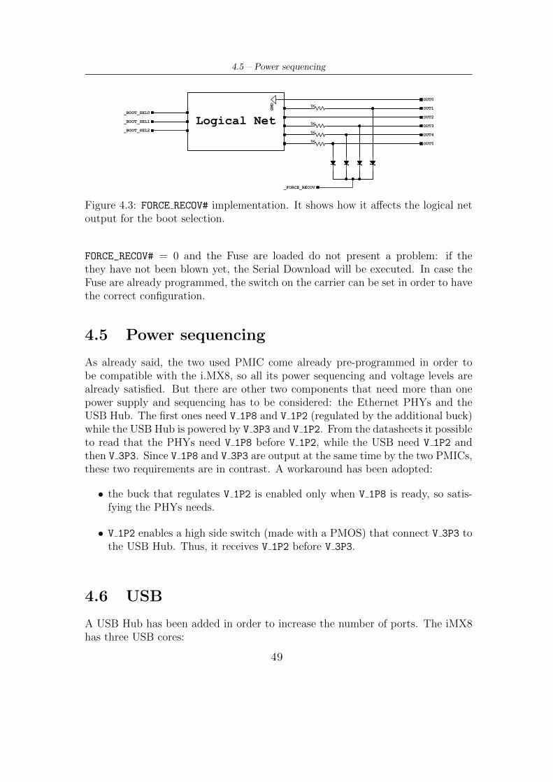
FORCE_RECOV# is not asserted.
In order to add this feature, it is necessary to notice that when FORCE_RECOV# =0 than SCU_BOOT_MODE = 000100: in other words all bits but SCU_BOOT_MODE2
are driven to 0. Remember that the USB Serial Download is enabled whenSCU_BOOT_MODE = 000100 but also when SCU_BOOT_MODE = 000000: this con-figuration load the fuses, but if they have not been programmed yet, the Serialdownload is executed instead. So a possible solution that minimizes the number oflogic gates is to use FORCE_RECOV# to pull down all signals that must be driven lowwhile leaving SCU_BOOT_MODE2 as is. This solution is shown in Fig. 4.4. Diodeshave been inserted in order to prevent current from flowing back to the carrier.
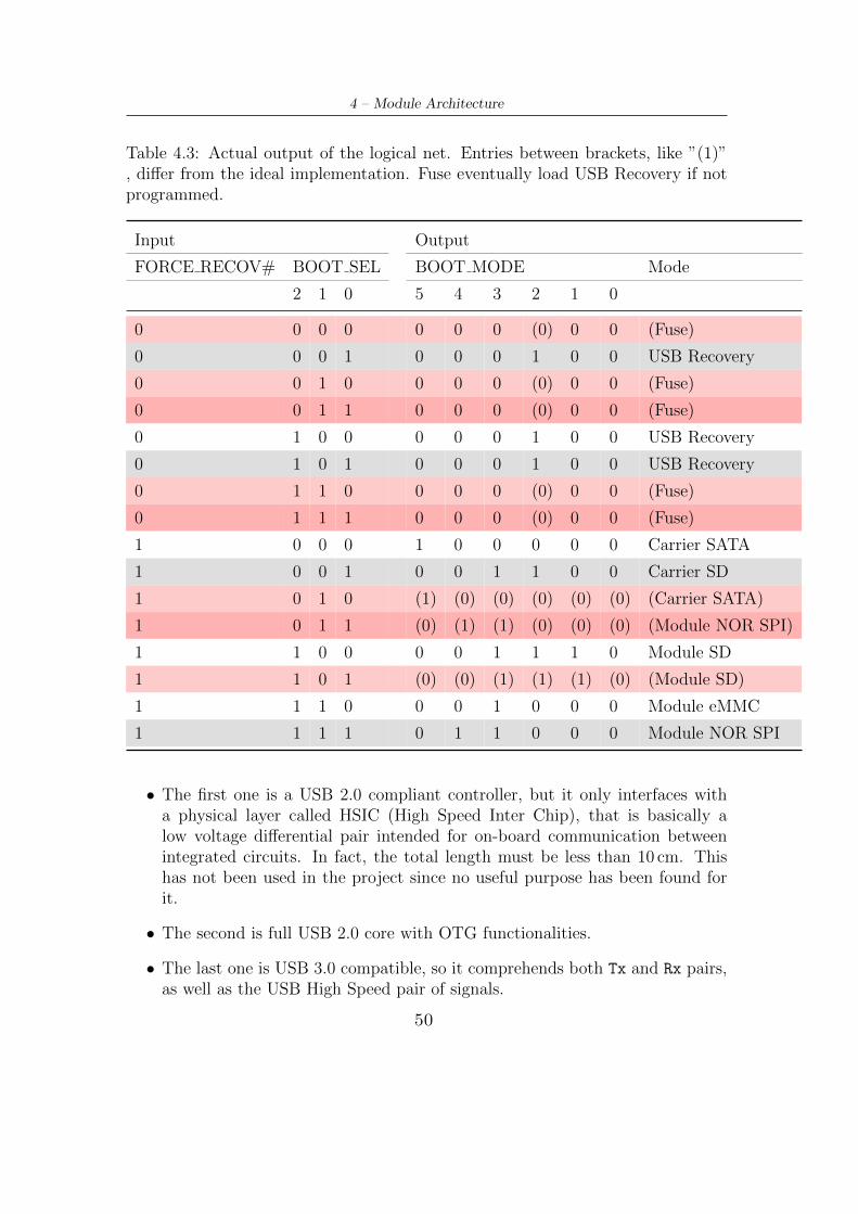
The actual and final output of the net is shown in Tab. 4.3. Rows in redare the one differing from the ideal output. Remember that the case where
48
4.5 – Power sequencing
Logical Net1K
1K
1K
1K
_FORCE_RECOV
GND
_BOOT_SEL0
_BOOT_SEL1
_BOOT_SEL2
OUT1
OUT2
OUT3
OUT4
OUT5
OUT0
Figure 4.3: FORCE RECOV# implementation. It shows how it affects the logical netoutput for the boot selection.
FORCE_RECOV# = 0 and the Fuse are loaded do not present a problem: if thethey have not been blown yet, the Serial Download will be executed. In case theFuse are already programmed, the switch on the carrier can be set in order to havethe correct configuration.
4.5 Power sequencing
As already said, the two used PMIC come already pre-programmed in order tobe compatible with the i.MX8, so all its power sequencing and voltage levels arealready satisfied. But there are other two components that need more than onepower supply and sequencing has to be considered: the Ethernet PHYs and theUSB Hub. The first ones need V 1P8 and V 1P2 (regulated by the additional buck)while the USB Hub is powered by V 3P3 and V 1P2. From the datasheets it possibleto read that the PHYs need V 1P8 before V 1P2, while the USB need V 1P2 andthen V 3P3. Since V 1P8 and V 3P3 are output at the same time by the two PMICs,these two requirements are in contrast. A workaround has been adopted:
• the buck that regulates V 1P2 is enabled only when V 1P8 is ready, so satis-fying the PHYs needs.
• V 1P2 enables a high side switch (made with a PMOS) that connect V 3P3 tothe USB Hub. Thus, it receives V 1P2 before V 3P3.
4.6 USB
A USB Hub has been added in order to increase the number of ports. The iMX8has three USB cores:
49
4 – Module Architecture
Table 4.3: Actual output of the logical net. Entries between brackets, like ”(1)”, differ from the ideal implementation. Fuse eventually load USB Recovery if notprogrammed.
Input Output
FORCE RECOV# BOOT SEL BOOT MODE Mode
2 1 0 5 4 3 2 1 0
0 0 0 0 0 0 0 (0) 0 0 (Fuse)
0 0 0 1 0 0 0 1 0 0 USB Recovery
0 0 1 0 0 0 0 (0) 0 0 (Fuse)
0 0 1 1 0 0 0 (0) 0 0 (Fuse)
0 1 0 0 0 0 0 1 0 0 USB Recovery
0 1 0 1 0 0 0 1 0 0 USB Recovery
0 1 1 0 0 0 0 (0) 0 0 (Fuse)
0 1 1 1 0 0 0 (0) 0 0 (Fuse)
1 0 0 0 1 0 0 0 0 0 Carrier SATA
1 0 0 1 0 0 1 1 0 0 Carrier SD
1 0 1 0 (1) (0) (0) (0) (0) (0) (Carrier SATA)
1 0 1 1 (0) (1) (1) (0) (0) (0) (Module NOR SPI)
1 1 0 0 0 0 1 1 1 0 Module SD
1 1 0 1 (0) (0) (1) (1) (1) (0) (Module SD)
1 1 1 0 0 0 1 0 0 0 Module eMMC
1 1 1 1 0 1 1 0 0 0 Module NOR SPI
• The first one is a USB 2.0 compliant controller, but it only interfaces witha physical layer called HSIC (High Speed Inter Chip), that is basically alow voltage differential pair intended for on-board communication betweenintegrated circuits. In fact, the total length must be less than 10 cm. Thishas not been used in the project since no useful purpose has been found forit.
• The second is full USB 2.0 core with OTG functionalities.
• The last one is USB 3.0 compatible, so it comprehends both Tx and Rx pairs,as well as the USB High Speed pair of signals.
50
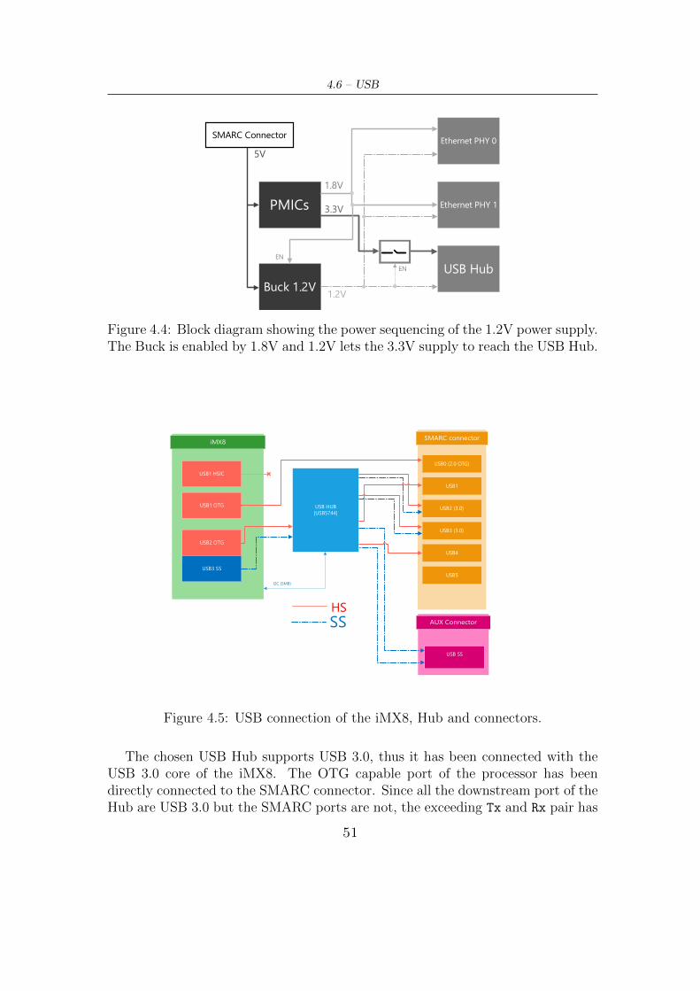
4.6 – USB
SMARC Connector
5V
PMICs
Ethernet PHY 0
Ethernet PHY 1
USB Hub
1.8V
Buck 1.2V 1.2V
EN
EN
3.3V
Figure 4.4: Block diagram showing the power sequencing of the 1.2V power supply.The Buck is enabled by 1.8V and 1.2V lets the 3.3V supply to reach the USB Hub.
USB1 HSIC
USB1 OTG
USB2 OTG
USB3 SS
USB HUB[USB5744]
USB0 (2.0 OTG)
USB1
USB2 (3.0)
USB3 (3.0)
USB4
USB5
HSSS
USB SS
I2C (SMB)
Figure 4.5: USB connection of the iMX8, Hub and connectors.
The chosen USB Hub supports USB 3.0, thus it has been connected with theUSB 3.0 core of the iMX8. The OTG capable port of the processor has beendirectly connected to the SMARC connector. Since all the downstream port of theHub are USB 3.0 but the SMARC ports are not, the exceeding Tx and Rx pair has
51

4 – Module Architecture
been routed to the Auxiliary connector: in this way, the carrier may re-join the2.0 and the 3.0 signals of the same port, thus having a complete 3.0 port. If onlythe 2.0 signals are used, the related 3.0 pairs must be left unconnected.
The Hub presents a SMB interface for configuration register access from theprocessor. These pins have been connected to a I2C of the iMX8 since the controlleralso supports SMB.
For each USB port present on the SMARC connector there is a EN_OC signalthat has a double role: it is pulled up by the module in order to enable a switchconnecting +5V to the device; and it is pulled low by the switch to signal anover current condition. This feature is compatible with the pin of the Hub calledPRT_CTRL that has the exact same behavior; so they can be directly connected.The same thing can not be done for the USB connected directly to the SMARCconnector : in fact the processor presents one pin for enabling the power deliveryand one pin for detecting the over current condition. In order to get the rightbehaviour, the pins has been connected together to form a single line, with theaddition of a diode preventing sourcing current from the EN pin.
Table 4.4: USB Assignement
iMX8 peripheral HUB port SMARC port Aux Connector
USB OTG1 - USB0 -
USB OTG2
+
USB SS3
HS1USB2
-
SS1 -
HS2USB3
-
SS2 -
HS3 USB1 -
SS3 - HUB3
HS4 USB4 -
SS4 - HUB4
4.7 HDMI and DisplayPort
The iMX8 has multi-protocol core that can manage several protocols, one at atime. It can manage:
• HDMI, both version 1.4 and 2.
52
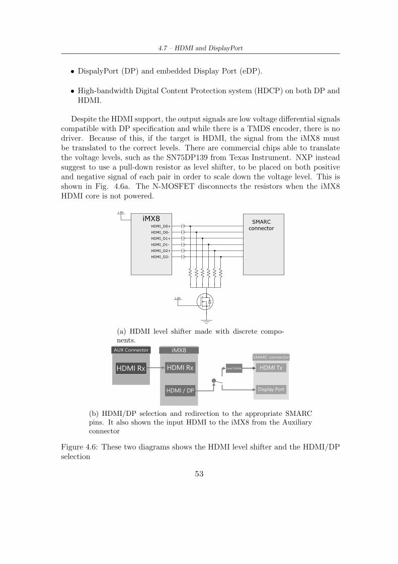
4.7 – HDMI and DisplayPort
• DispalyPort (DP) and embedded Display Port (eDP).
• High-bandwidth Digital Content Protection system (HDCP) on both DP andHDMI.
Despite the HDMI support, the output signals are low voltage differential signalscompatible with DP specification and while there is a TMDS encoder, there is nodriver. Because of this, if the target is HDMI, the signal from the iMX8 mustbe translated to the correct levels. There are commercial chips able to translatethe voltage levels, such as the SN75DP139 from Texas Instrument. NXP insteadsuggest to use a pull-down resistor as level shifter, to be placed on both positiveand negative signal of each pair in order to scale down the voltage level. This isshown in Fig. 4.6a. The N-MOSFET disconnects the resistors when the iMX8HDMI core is not powered.
iMX8
1.8V
1.8V
HDMI_D0+
HDMI_D0-
SMARCconnector
HDMI_D1+
HDMI_D1-
HDMI_D2+
HDMI_D2-
(a) HDMI level shifter made with discrete compo-nents.
HDMI Rx
HDMI / DP
HDMI Tx
Display Port
HDMI Rx Level Shifter
(b) HDMI/DP selection and redirection to the appropriate SMARCpins. It also shown the input HDMI to the iMX8 from the Auxiliaryconnector
Figure 4.6: These two diagrams shows the HDMI level shifter and the HDMI/DPselection
53
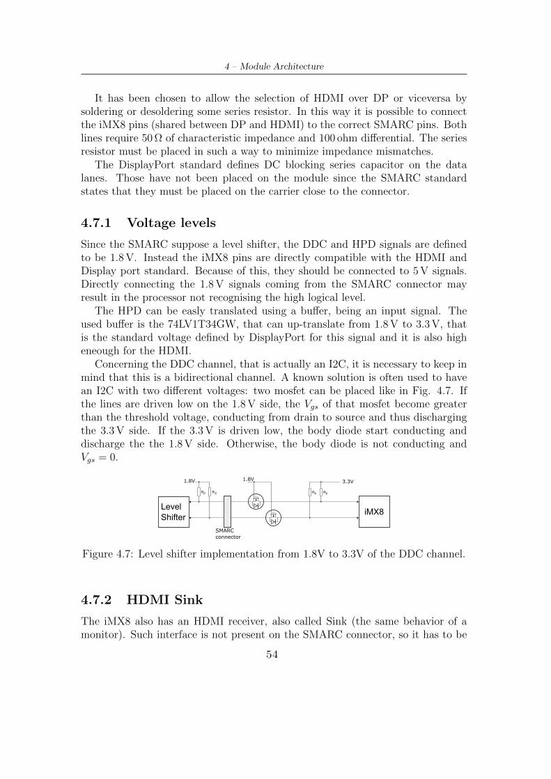
4 – Module Architecture
It has been chosen to allow the selection of HDMI over DP or viceversa bysoldering or desoldering some series resistor. In this way it is possible to connectthe iMX8 pins (shared between DP and HDMI) to the correct SMARC pins. Bothlines require 50Ω of characteristic impedance and 100 ohm differential. The seriesresistor must be placed in such a way to minimize impedance mismatches.
The DisplayPort standard defines DC blocking series capacitor on the datalanes. Those have not been placed on the module since the SMARC standardstates that they must be placed on the carrier close to the connector.
4.7.1 Voltage levels
Since the SMARC suppose a level shifter, the DDC and HPD signals are definedto be 1.8V. Instead the iMX8 pins are directly compatible with the HDMI andDisplay port standard. Because of this, they should be connected to 5V signals.Directly connecting the 1.8V signals coming from the SMARC connector mayresult in the processor not recognising the high logical level.
The HPD can be easly translated using a buffer, being an input signal. Theused buffer is the 74LV1T34GW, that can up-translate from 1.8V to 3.3V, thatis the standard voltage defined by DisplayPort for this signal and it is also higheneough for the HDMI.
Concerning the DDC channel, that is actually an I2C, it is necessary to keep inmind that this is a bidirectional channel. A known solution is often used to havean I2C with two different voltages: two mosfet can be placed like in Fig. 4.7. Ifthe lines are driven low on the 1.8V side, the Vgs of that mosfet become greaterthan the threshold voltage, conducting from drain to source and thus dischargingthe 3.3V side. If the 3.3V is driven low, the body diode start conducting anddischarge the the 1.8V side. Otherwise, the body diode is not conducting andVgs = 0.
Rp Rp RpRp
1.8V 3.3V
iMX8LevelShifter
1.8V
SMARCconnector
Figure 4.7: Level shifter implementation from 1.8V to 3.3V of the DDC channel.
4.7.2 HDMI Sink
The iMX8 also has an HDMI receiver, also called Sink (the same behavior of amonitor). Such interface is not present on the SMARC connector, so it has to be
54
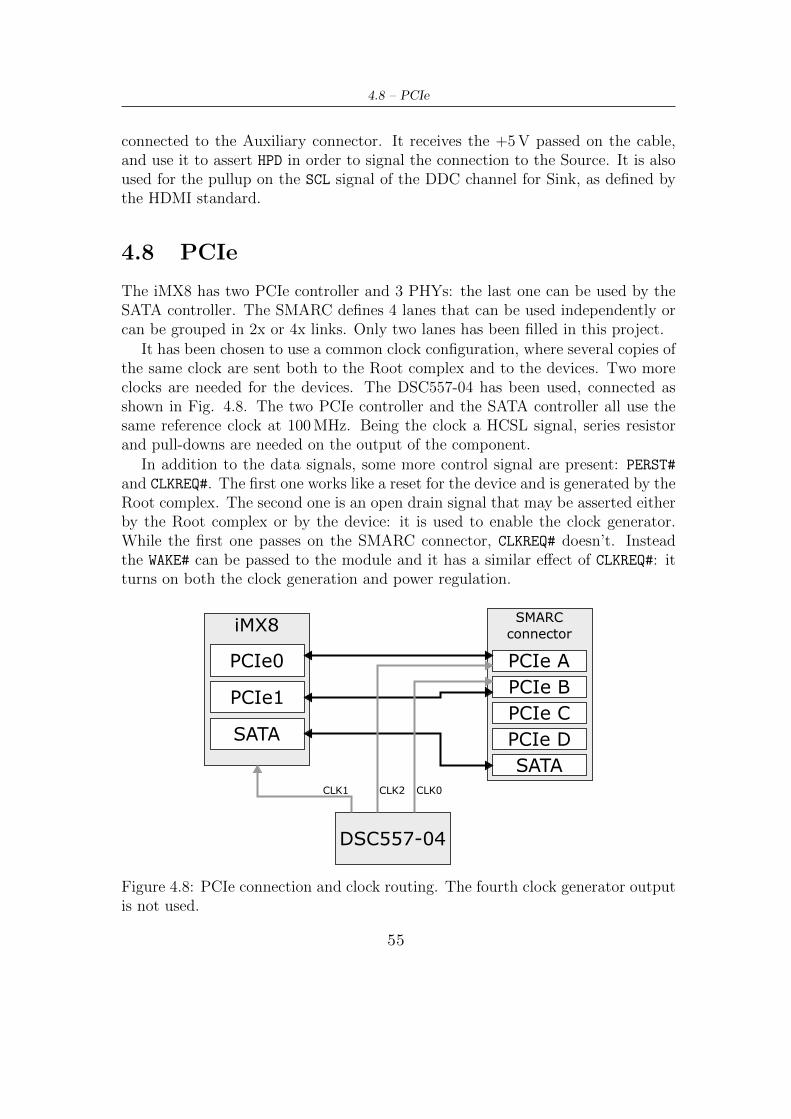
4.8 – PCIe
connected to the Auxiliary connector. It receives the +5V passed on the cable,and use it to assert HPD in order to signal the connection to the Source. It is alsoused for the pullup on the SCL signal of the DDC channel for Sink, as defined bythe HDMI standard.
4.8 PCIe
The iMX8 has two PCIe controller and 3 PHYs: the last one can be used by theSATA controller. The SMARC defines 4 lanes that can be used independently orcan be grouped in 2x or 4x links. Only two lanes has been filled in this project.
It has been chosen to use a common clock configuration, where several copies ofthe same clock are sent both to the Root complex and to the devices. Two moreclocks are needed for the devices. The DSC557-04 has been used, connected asshown in Fig. 4.8. The two PCIe controller and the SATA controller all use thesame reference clock at 100MHz. Being the clock a HCSL signal, series resistorand pull-downs are needed on the output of the component.
In addition to the data signals, some more control signal are present: PERST#
and CLKREQ#. The first one works like a reset for the device and is generated by theRoot complex. The second one is an open drain signal that may be asserted eitherby the Root complex or by the device: it is used to enable the clock generator.While the first one passes on the SMARC connector, CLKREQ# doesn’t. Insteadthe WAKE# can be passed to the module and it has a similar effect of CLKREQ#: itturns on both the clock generation and power regulation.
iMX8
PCIe0
PCIe1
SATA
DSC557-04
SMARCconnector
PCIe APCIe BPCIe CPCIe DSATA
CLK1 CLK2 CLK0
Figure 4.8: PCIe connection and clock routing. The fourth clock generator outputis not used.
55
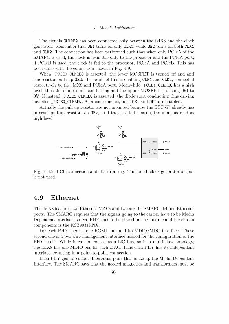
4 – Module Architecture
The signals CLKREQ has been connected only between the iMX8 and the clockgenerator. Remember that OE1 turns on only CLK0, while OE2 turns on both CLK1
and CLK2. The connection has been performed such that when only PCIeA of theSMARC is used, the clock is available only to the processor and the PCIeA port;if PCIeB is used, the clock is fed to the processor, PCIeA and PCIeB. This hasbeen done with the connection shown in Fig. 4.9.
When _PCIE0_CLKREQ is asserted, the lower MOSFET is turned off and andthe resistor pulls up OE2: the result of this is enabling CLK1 and CLK2, connectedrespectively to the iMX8 and PCIeA port. Meanwhile _PCIE1_CLKREQ has a highlevel, thus the diode is not conducting and the upper MOSFET is driving OE1 to0V. If instead _PCIE1_CLKREQ is asserted, the diode start conducting thus drivinglow also _PCIE0_CLKREQ. As a consequence, both OE1 and OE2 are enabled.
Actually the pull up resistor are not mounted because the DSC557 already hasinternal pull-up resistors on OEx, so if they are left floating the input as read ashigh level.
22
6
1
53
4
GND
GND
_PCIE0_CLKREQ
_PCIE1_CLKREQ
V_3P3V_3P3
OE1
OE21
CLK0
CLK1
CLK2
PCIeB
iMX8
PCIeA
Figure 4.9: PCIe connection and clock routing. The fourth clock generator outputis not used.
4.9 Ethernet
The iMX8 features two Ethernet MACs and two are the SMARC defined Ethernetports. The SMARC requires that the signals going to the carrier have to be MediaDependent Interface, so two PHYs has to be placed on the module and the chosencomponents is the KSZ9031RNX.
For each PHY there is one RGMII bus and its MDIO/MDC interface. Thesesecond one is a two wire management interface needed for the configuration of thePHY itself. While it can be routed as a I2C bus, so in a multi-slave topology,the iMX8 has one MDIO bus for each MAC. Thus each PHY has its independentinterface, resulting in a point-to-point connection.
Each PHY generates four differential pairs that make up the Media DependentInterface. The SMARC says that the needed magnetics and transformers must be
56
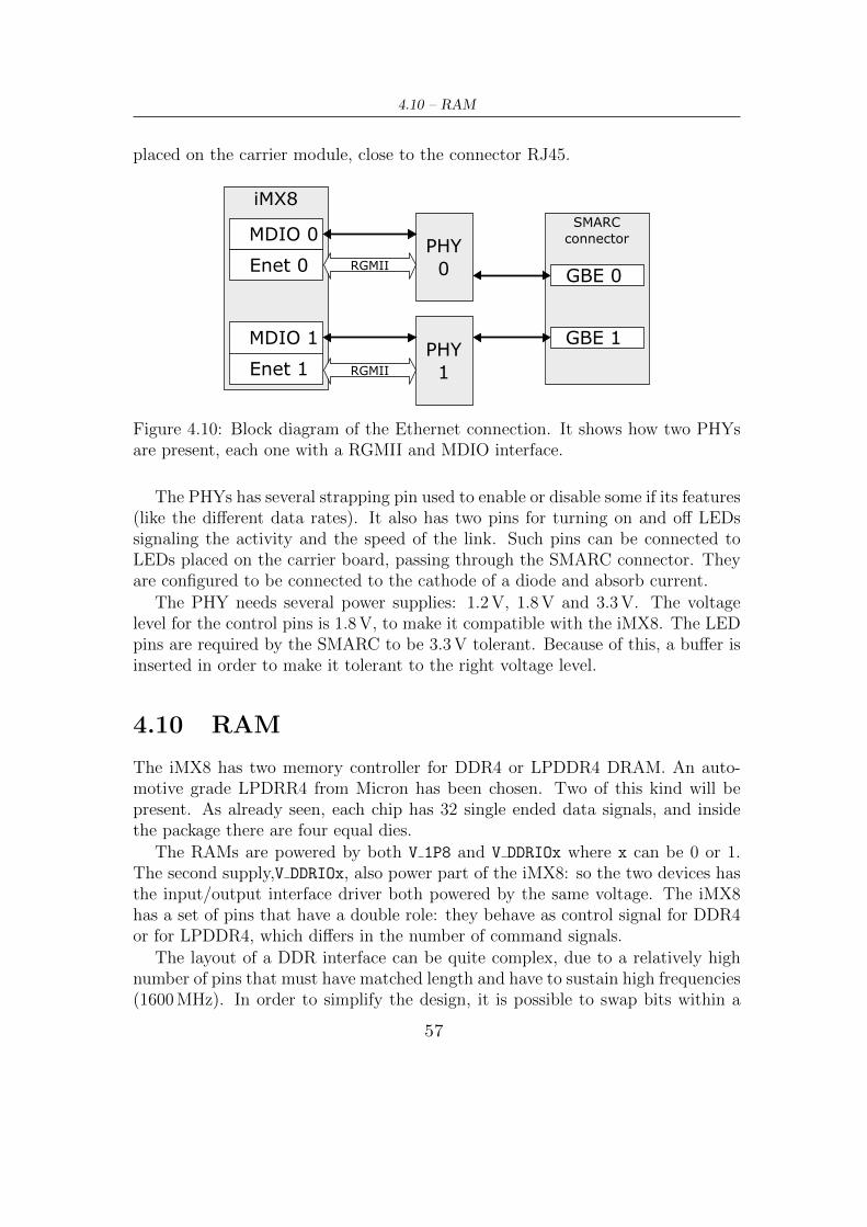
4.10 – RAM
placed on the carrier module, close to the connector RJ45.
iMX8
MDIO 0
Enet 0
SMARCconnector
GBE 0
GBE 1MDIO 1
Enet 1
PHY0
PHY1
RGMII
RGMII
Figure 4.10: Block diagram of the Ethernet connection. It shows how two PHYsare present, each one with a RGMII and MDIO interface.
The PHYs has several strapping pin used to enable or disable some if its features(like the different data rates). It also has two pins for turning on and off LEDssignaling the activity and the speed of the link. Such pins can be connected toLEDs placed on the carrier board, passing through the SMARC connector. Theyare configured to be connected to the cathode of a diode and absorb current.
The PHY needs several power supplies: 1.2V, 1.8V and 3.3V. The voltagelevel for the control pins is 1.8V, to make it compatible with the iMX8. The LEDpins are required by the SMARC to be 3.3V tolerant. Because of this, a buffer isinserted in order to make it tolerant to the right voltage level.
4.10 RAM
The iMX8 has two memory controller for DDR4 or LPDDR4 DRAM. An auto-motive grade LPDRR4 from Micron has been chosen. Two of this kind will bepresent. As already seen, each chip has 32 single ended data signals, and insidethe package there are four equal dies.
The RAMs are powered by both V 1P8 and V DDRIOx where x can be 0 or 1.The second supply,V DDRIOx, also power part of the iMX8: so the two devices hasthe input/output interface driver both powered by the same voltage. The iMX8has a set of pins that have a double role: they behave as control signal for DDR4or for LPDDR4, which differs in the number of command signals.
The layout of a DDR interface can be quite complex, due to a relatively highnumber of pins that must have matched length and have to sustain high frequencies(1600MHz). In order to simplify the design, it is possible to swap bits within a
57
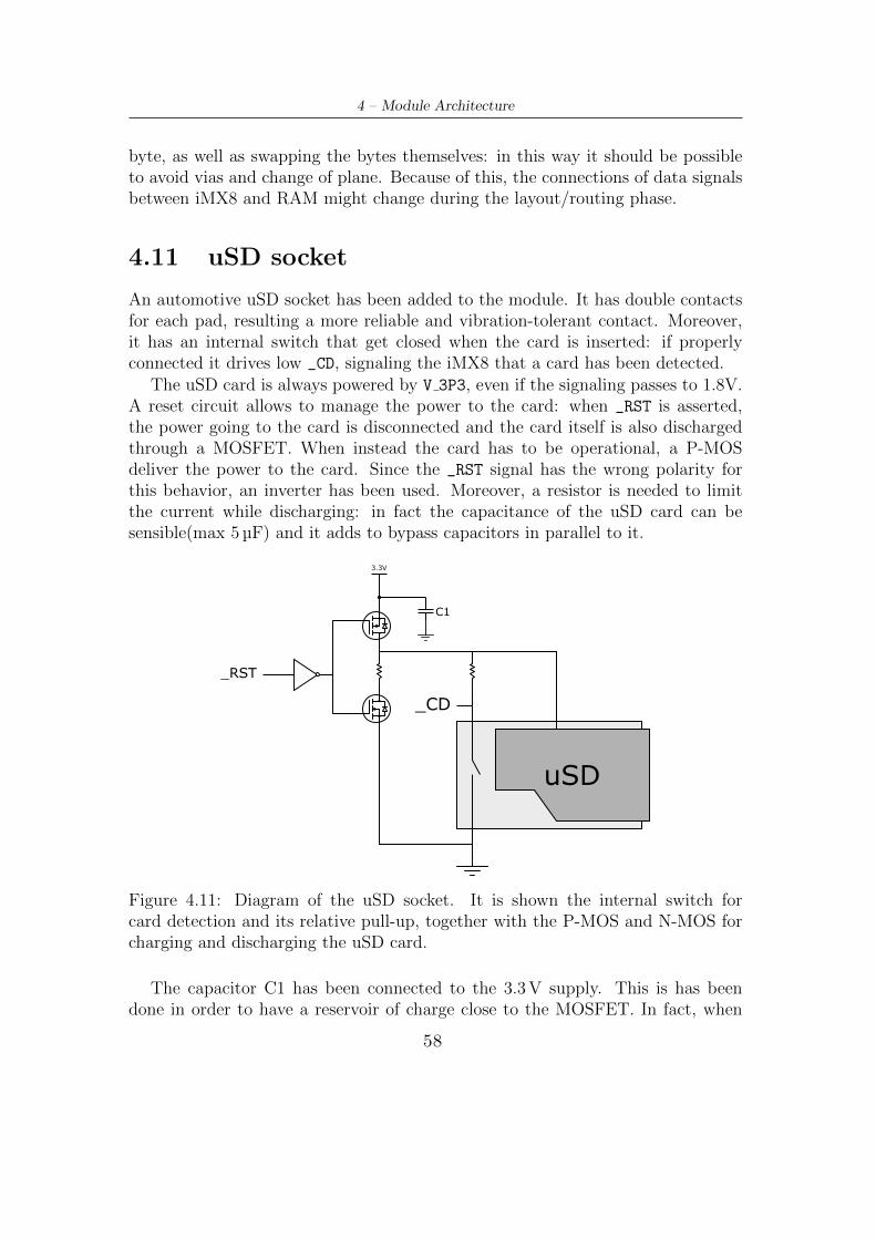
4 – Module Architecture
byte, as well as swapping the bytes themselves: in this way it should be possibleto avoid vias and change of plane. Because of this, the connections of data signalsbetween iMX8 and RAM might change during the layout/routing phase.
4.11 uSD socket
An automotive uSD socket has been added to the module. It has double contactsfor each pad, resulting a more reliable and vibration-tolerant contact. Moreover,it has an internal switch that get closed when the card is inserted: if properlyconnected it drives low _CD, signaling the iMX8 that a card has been detected.
The uSD card is always powered by V 3P3, even if the signaling passes to 1.8V.A reset circuit allows to manage the power to the card: when _RST is asserted,the power going to the card is disconnected and the card itself is also dischargedthrough a MOSFET. When instead the card has to be operational, a P-MOSdeliver the power to the card. Since the _RST signal has the wrong polarity forthis behavior, an inverter has been used. Moreover, a resistor is needed to limitthe current while discharging: in fact the capacitance of the uSD card can besensible(max 5 µF) and it adds to bypass capacitors in parallel to it.
uSD
_CD
3.3V
_RST
C1
Figure 4.11: Diagram of the uSD socket. It is shown the internal switch forcard detection and its relative pull-up, together with the P-MOS and N-MOS forcharging and discharging the uSD card.
The capacitor C1 has been connected to the 3.3V supply. This is has beendone in order to have a reservoir of charge close to the MOSFET. In fact, when
58
4.12 – Reset Behaviour
the p-MOS starts conducting, a peak of in-rush current can be present, due tothe large load capacitance of about 10 µF. In this way, the charge needed is takenfrom C1 that is always connected to the power supply. This should prevent highpeaks of absorption from the 3.3V that may result in a temporary voltage drop.
4.12 Reset Behaviour
The reset structure has to be considered carefully. In fact there are several resetsources:
• The PMIC asserts the reset signals until all voltage levels are at their correctvalue.
• The iMX8 has to be able to reset itself together with all the other components.
• The SMARC defines a RST_IN driven by the carrier that should reset themodule
• A JTAG connector is present on the module for software development anddebugging: this interface comprehends a reset signal.
A general reset signal is present and it is called _RST. It can be driven lowby the PMIC, trough its pin RESETBMCU. It asserts this signal during power-on,as well as when a watchdog event is triggered. This happen if the iMX8 fails torefresh a countdown timer within a certain time. The processor can also triggerthe watchdog event asserting SCU_WDOG_OUT. In this way the iMX8 is able to resetitself in case of failure.
The SMARC signal _RST_IN and the TRST from JTAG connector as connectedwith a diode to _RST. In this way, when one of them is driven low, the correspondingdiode starts conducting thus discharging the line and asserting _RST. The effectof this is the resetting of the Ethernet PHYs, the NOR Flash and the iMX8. ThePHYs can also be reset independently using a GPIO of the processor.
The USB Hub instead is only reset by a GPIO, since it has its own internaltimer for power-on reset. On the other hand, the NOR Flash is reset only by the_POR since the processor can reset it through SPI commands.
4.13 JTAG
The JTAG interface (defined by the Joint Test Action Group) is an interface fortesting and debugging a whole system after manufacturing. Born for boundary-scan of the ICs in order to test connections to the PCB and package, has becomethe interface to use during software development. In fact, a simple 4 pin interface
59
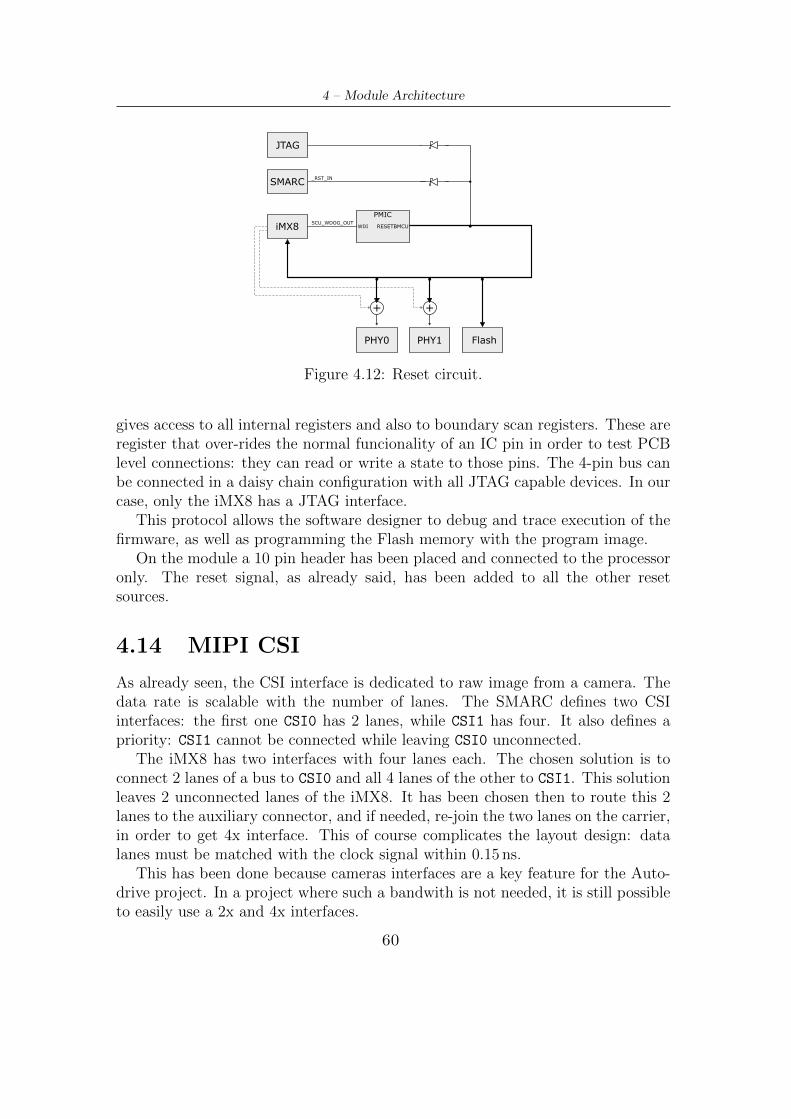
4 – Module Architecture
_RST_INSMARC
JTAG
iMX8PMIC
WDI RESETBMCU
FlashPHY1PHY0
+ +
SCU_WDOG_OUT
Figure 4.12: Reset circuit.
gives access to all internal registers and also to boundary scan registers. These areregister that over-rides the normal funcionality of an IC pin in order to test PCBlevel connections: they can read or write a state to those pins. The 4-pin bus canbe connected in a daisy chain configuration with all JTAG capable devices. In ourcase, only the iMX8 has a JTAG interface.
This protocol allows the software designer to debug and trace execution of thefirmware, as well as programming the Flash memory with the program image.
On the module a 10 pin header has been placed and connected to the processoronly. The reset signal, as already said, has been added to all the other resetsources.
4.14 MIPI CSI
As already seen, the CSI interface is dedicated to raw image from a camera. Thedata rate is scalable with the number of lanes. The SMARC defines two CSIinterfaces: the first one CSI0 has 2 lanes, while CSI1 has four. It also defines apriority: CSI1 cannot be connected while leaving CSI0 unconnected.
The iMX8 has two interfaces with four lanes each. The chosen solution is toconnect 2 lanes of a bus to CSI0 and all 4 lanes of the other to CSI1. This solutionleaves 2 unconnected lanes of the iMX8. It has been chosen then to route this 2lanes to the auxiliary connector, and if needed, re-join the two lanes on the carrier,in order to get 4x interface. This of course complicates the layout design: datalanes must be matched with the clock signal within 0.15 ns.
This has been done because cameras interfaces are a key feature for the Auto-drive project. In a project where such a bandwith is not needed, it is still possibleto easily use a 2x and 4x interfaces.
60
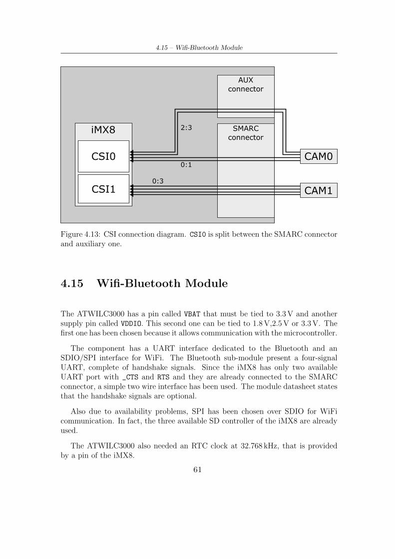
4.15 – Wifi-Bluetooth Module
iMX8
CSI0
CSI1
SMARCconnector
AUXconnector
CAM0
CAM10:3
2:3
0:1
Figure 4.13: CSI connection diagram. CSI0 is split between the SMARC connectorand auxiliary one.
4.15 Wifi-Bluetooth Module
The ATWILC3000 has a pin called VBAT that must be tied to 3.3V and anothersupply pin called VDDIO. This second one can be tied to 1.8V,2.5V or 3.3V. Thefirst one has been chosen because it allows communication with the microcontroller.
The component has a UART interface dedicated to the Bluetooth and anSDIO/SPI interface for WiFi. The Bluetooth sub-module present a four-signalUART, complete of handshake signals. Since the iMX8 has only two availableUART port with _CTS and RTS and they are already connected to the SMARCconnector, a simple two wire interface has been used. The module datasheet statesthat the handshake signals are optional.
Also due to availability problems, SPI has been chosen over SDIO for WiFicommunication. In fact, the three available SD controller of the iMX8 are alreadyused.
The ATWILC3000 also needed an RTC clock at 32.768 kHz, that is providedby a pin of the iMX8.
61
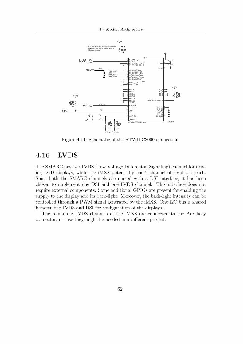
4 – Module Architecture
NC_4NC_3NC_5NC_6
VBAT
RTC_CLK
BT_CTS/I2C_SCL_SBT_RTS/I2C_SDA_S
BT_RXDBT_TXD
_RESET
SD_CLK/GPIO8SD_CMD/SPI_SCKSD_DAT0/SPI_MISOSD_DAT1/SPI_SSNSD_DAT2/SPI_MOSISD_DAT3/GPIO7
EP_GND
GND_36GND_28GND_13GND_1
GND_21CHIP_EN
UART_RXDUART_TXD
VDDIO
_SDIO_CFG/SPI_CFG
GPIO0GPIO3GPIO4GPIO17GPIO18GPIO19GPIO20GPIO21
_IRQ
WiFi
BT
33
3532313029151434
2
12
1617
19211132836
37
272625242322
7
89
1011
20
18
6534
ATWILC3000-MR110CA GND
V_1P8
V_1P8
RTC_CK
_IRQ
_RST
EN
SPI2
SPI2_CS0
SPI2_SCKSPI2_SDI
SPI2_SDO
V_1P8
No more UART with CTS/RTS available:make the Chip see an always asserted"Request to send"
V_1P8
GNDGND
U13
V_3P3
Figure 4.14: Schematic of the ATWILC3000 connection.
4.16 LVDS
The SMARC has two LVDS (Low Voltage Differential Signaling) channel for driv-ing LCD displays, while the iMX8 potentially has 2 channel of eight bits each.Since both the SMARC channels are muxed with a DSI interface, it has beenchosen to implement one DSI and one LVDS channel. This interface does notrequire external components. Some additional GPIOs are present for enabling thesupply to the display and its back-light. Moreover, the back-light intensity can becontrolled through a PWM signal generated by the iMX8. One I2C bus is sharedbetween the LVDS and DSI for configuration of the displays.
The remaining LVDS channels of the iMX8 are connected to the Auxiliaryconnector, in case they might be needed in a different project.
62
Chapter 5
Conclusions
Starting from the non-strict requirements, a general purpose board has been de-veloped. The standard SMARC has been chosen to get interoperability with othermodules. The design started from the understanding of the i.MX8 capabilities andits interfaces. A study of all standard interfaces was needed. Then component hasbeen looked for and chosen to match both the processor and the SMARC standard.The project has been developed up to the schematic level.
5.1 Future implementations
The project will pass to the layout and routing phase. Particular attention will beneeded for the reduced board size and the high-speed interfaces. Having to dealwith frequencies above 1GHz, connections has to be considered as transmissionlines. Moreover, a simulator is needed for trouble shooting the connections duringdesign phase.
The first step is the definition of a stack-up, that is the definition of all layerscomposing the PCB. It must take in consideration the needed impedances: thedielectric thickness heavily influence the trace width given a target impedance.Moreover, ground and power planes will be defined during this phase. Since allhigh-speed traces need a return path, all traces are routed close to a ground plane,resulting in a microstrip or stripline structures. Because of this, several groundplanes will be inserted, interleaved with signal ones. The SMARC requires thatthe total PCB height must be 1.2mm so to be inserted in the MXM3 connector.
Moreover, the fine pitch BGA of the iMX8 impose a minimum number of layerfor the break-out of the signals. As a rule of thumb, the number of needed layercan be estimated considering the number of signals to be routed out of the BGAand the number of available ”channels”, which is the space between balls wherea trace can be routed. The formula is layers = signals
channels. Considering the iMX8
63
5 – Conclusions
package, the number of channels is 26 per side, so 26 · 4 = 104 and the numberof signal is total − powerP in = 1313 − 719 = 594. So, substituting in the firstformula:
layers =signals
channels=
594
104≃ 5.71 ≃ 6
Therefore, a stackup where 6 signal layers are present may be a good startingpoint.
Moreover, the required impedances has to be considered: the main part ofdifferential pairs need an impedance of 50Ω single ended and 100Ω differential,but also 85Ω and 90Ω are needed. Another aspect to consider of the stackupis the inter-plane capacitance that results from two parallel planes separted by adielectric. This phenomenon can be exploited to get a low inductance capacitancebetween a ground and a power planes adjacent to each other. This capacitanceadds to the bypass capacitors, thus reducing the noise on the power supply.
The routing phase has to be done respecting some indications. The returnpath of signals is an important concept to consider: it is the path that takes thecurrent flowing in the opposite direction of the signal propagation. The path takeninfluence the area of the loop of current: with a solid reference plane, the currentwould take the least impedance path. But if some split in the plane are present, thecurrent may be forced to take different path, increasing the loop area and than theElectromagnetic Emissions. [5] Moreover, the trace-width has to be kept constantin order to minimize impedance mismatches that would results in reflection andperformance degradation.
In order to keep the common mode rejection benefits of a differential signaling,the two signals has to have an exact phase difference of 180°, and this may notbe true in case of length mismatches, trace width differences or local dielectricdifferences. An example of this last cause is the Fiber Weave Effect, consisting indielectric constant differences based on the presence or absence of glass fiber inthe layer between the signal trace and the reference plane. If the two traces havedifferent impedances, the phase velocity will not be the same. This effect can beavoided by using a a material with tighter glass fiber weave.
All this considerations have to be kept in mind while trying to satisfy all thetiming specifications of the standard interfaces.
64
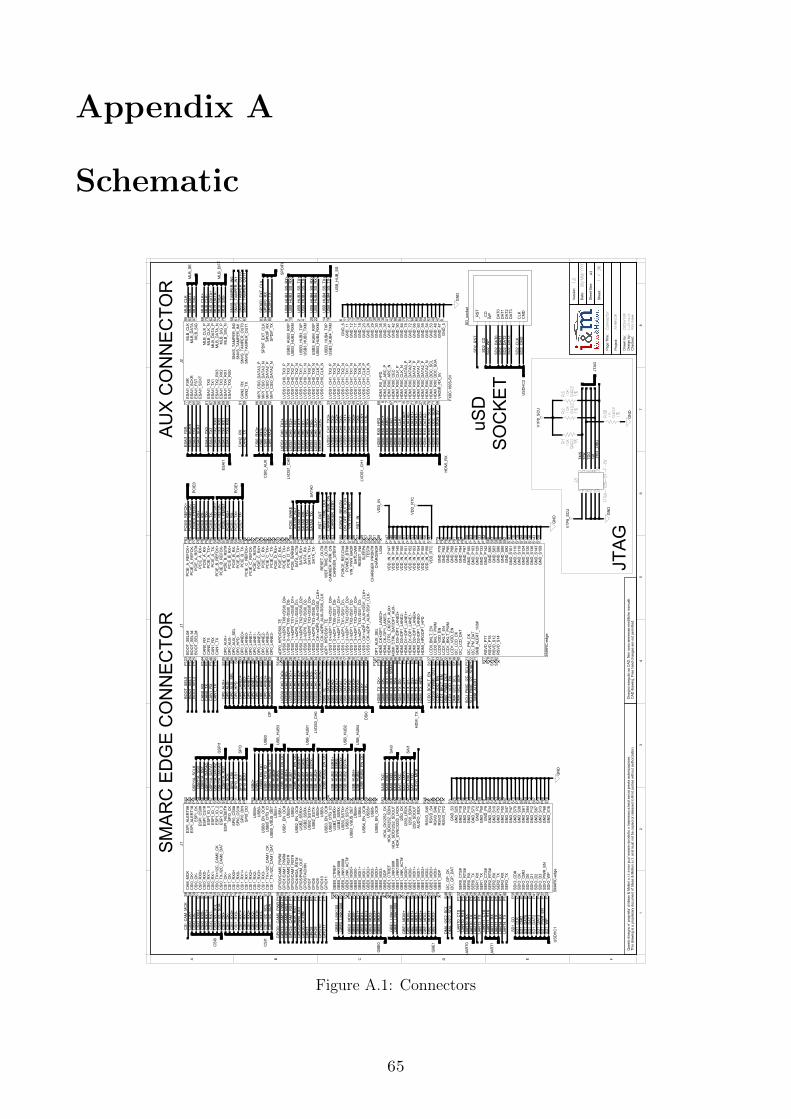
Appendix A
Schematic
Dra
wn
by:
Che
cked
:D
esig
n by
:
Proj
ect:
Shee
t Siz
e:
Page
Titl
e:
Shee
t:
Dat
e:
Vers
ion:
CAD
dra
win
g. F
ree
hand
cha
nges
are
not
per
mitt
ed.
Dis
egno
ese
guito
su
CAD
. Non
son
o am
mes
se m
odifi
che
man
uali.
This
dra
win
g is
a p
ropr
ieta
ry d
ocum
ent o
f Ide
as &
Mot
ion
s.r.l
. and
mus
t not
be
copi
ed o
r rel
ease
d to
third
par
ties
with
out a
utho
rizat
ion.
Que
sto
dise
gno
e' p
ropr
ieta
' di I
deas
& M
otio
n s.
r.l. e
non
puo
' ess
ere
ripro
dotto
o tr
asm
esso
a te
rzi s
enza
pre
via
auto
rizza
zion
e.
/A3
12
34
56
78
A B C D E F
Re
vie
we
r
Dra
ftm
an
iMX
8S
OM
L.
Gir
au
di
13
6
1.0
DD
/M
M/
YY
YY
Co
nn
ec
tor
ESAI
1_FS
R
ESAI
1_FS
TES
AI1_
SCKR
ESAI
1_SC
KT
ESAI
1_TX
0ES
AI1_
TX1
ESAI
1_TX
2_R
X3ES
AI1_
TX3_
RX2
ESAI
1_TX
4_R
X1ES
AI1_
TX5_
RX0
CAN
2_R
XC
AN2_
TX
VHD
MI_
RX_
5V
MIP
I_C
SI0_
DAT
A3_P
MIP
I_C
SI0_
DAT
A3_N
MIP
I_C
SI0_
DAT
A2_P
MIP
I_C
SI0_
DAT
A2_N
LVD
S1_C
H1_
TX3_
PLV
DS1
_CH
1_TX
3_N
LVD
S1_C
H1_
TX2_
PLV
DS1
_CH
1_TX
2_N
LVD
S1_C
H1_
TX1_
PLV
DS1
_CH
1_TX
1_N
LVD
S1_C
H1_
TX0_
PLV
DS1
_CH
1_TX
0_N
LVD
S1_C
H1_
CLK
_PLV
DS1
_CH
1_C
LK_N
LVD
S1_C
H0_
TX3_
PLV
DS1
_CH
0_TX
3_N
LVD
S1_C
H0_
TX2_
PLV
DS1
_CH
0_TX
2_N
LVD
S1_C
H0_
TX1_
PLV
DS1
_CH
0_TX
1_N
LVD
S1_C
H0_
TX0_
PLV
DS1
_CH
0_TX
0_N
LVD
S1_C
H0_
CLK
_PLV
DS1
_CH
0_C
LK_N
HD
MI_
RX_
HPD
HD
MI_
RX0
_AR
C_N
HD
MI_
RX0
_AR
C_P
HD
MI_
RX0
_CEC
HD
MI_
RX0
_CLK
_NH
DM
I_R
X0_C
LK_P
HD
MI_
RX0
_DAT
A0_N
HD
MI_
RX0
_DAT
A0_P
HD
MI_
RX0
_DAT
A1_N
HD
MI_
RX0
_DAT
A1_P
HD
MI_
RX0
_DAT
A2_N
HD
MI_
RX0
_DAT
A2_P
HD
MI_
RX0
_DD
C_S
CL
HD
MI_
RX0
_DD
C_S
DA
GN
D_6
GN
D_1
1G
ND
_12
GN
D_1
7G
ND
_18
GN
D_2
3G
ND
_24
GN
D_2
9G
ND
_30
GN
D_3
5G
ND
_36
GN
D_4
1G
ND
_42
GN
D_9
0G
ND
_84
GN
D_7
8G
ND
_72
GN
D_6
6G
ND
_60
GN
D_5
9G
ND
_54
GN
D_5
3G
ND
_48
GN
D_4
7G
ND
_5
MLB
_CLK
MLB
_CLK
_NM
LB_C
LK_P
MLB
_DAT
A
MLB
_DAT
A_N
MLB
_DAT
A_P
MLB
_SIG
MLB
_SIG
_NM
LB_S
IG_P
SNVS
_TAM
PER
_IN
0SN
VS_T
AMPE
R_I
N1
SNVS
_TAM
PER
_OU
T0SN
VS_T
AMPE
R_O
UT1
SPD
IF_E
XT_C
LKSP
DIF
_RX
SPD
IF_T
X
USB
3_H
UB3
_RXM
USB
3_H
UB3
_RXP
USB
3_H
UB3
_TXM
USB
3_H
UB3
_TXP
USB
3_H
UB4
_RXM
USB
3_H
UB4
_RXP
USB
3_H
UB4
_TXM
USB
3_H
UB4
_TXP
GN
D
LVD
S1_C
H0_
CLK
-LV
DS1
_CH
0_C
LK+
LVD
S1_C
H0_
TX0-
LVD
S1_C
H0_
TX0+
LVD
S1_C
H0_
TX1-
LVD
S1_C
H0_
TX1+
LVD
S1_C
H0_
TX2-
LVD
S1_C
H0_
TX2+
LVD
S1_C
H0_
TX3-
LVD
S1_C
H0_
TX3+
LVD
S1_C
H1_
CLK
-LV
DS1
_CH
1_C
LK+
LVD
S1_C
H1_
TX0-
LVD
S1_C
H1_
TX0+
LVD
S1_C
H1_
TX1-
LVD
S1_C
H1_
TX1+
LVD
S1_C
H1_
TX2-
LVD
S1_C
H1_
TX2+
LVD
S1_C
H1_
TX3-
LVD
S1_C
H1_
TX3+
CSI
0_AU
X
CSI
0_R
X3+
CSI
0_R
X3-
CSI
0_R
X2+
CSI
0_R
X2-
HD
MI_
RX
HD
MI_
RX0
_AR
C-
HD
MI_
RX0
_AR
C+
HD
MI_
RX0
_CEC
HD
MI_
RX0
_CLK
-H
DM
I_R
X0_C
LK+
HD
MI_
RX0
_DAT
A0-
HD
MI_
RX0
_DAT
A0+
HD
MI_
RX0
_DAT
A1-
HD
MI_
RX0
_DAT
A1+
HD
MI_
RX0
_DAT
A2-
HD
MI_
RX0
_DAT
A2+
HD
MI_
RX0
_DD
C_S
CL
HD
MI_
RX0
_DD
C_S
DA
HD
MI_
RX0
_HPD
HD
MI_
RX0
_MO
N_5
V
CAN
2_R
XC
AN2_
TX
ESAI
1
ESAI
1_FS
R
ESAI
1_FS
TES
AI1_
SCKR
ESAI
1_SC
KT
ESAI
1_TX
0ES
AI1_
TX1
ESAI
1_TX
2_R
X3ES
AI1_
TX3_
RX2
ESAI
1_TX
4_R
X1ES
AI1_
TX5_
RX0
MLB
_SE
MLB
_CLK
MLB
_DAT
AM
LB_S
IG
MLB
_DIF
F
MLB
_CLK
+M
LB_C
LK-
MLB
_DAT
A+M
LB_D
ATA-
MLB
_SIG
+M
LB_S
IG-
SNVS
_TAM
PER
_IN
0SN
VS_T
AMPE
R_I
N1
SNVS
_TAM
PER
_OU
T0SN
VS_T
AMPE
R_O
UT1
SPD
IF0_
EXT_
CLK
SPD
IF0_
RX
SPD
IF0_
TX
USB
_HU
B_SS
USB
_HU
B3_S
S_R
X-U
SB_H
UB3
_SS_
RX+
USB
_HU
B3_S
S_TX
-U
SB_H
UB3
_SS_
TX+
USB
_HU
B4_S
S_R
X-U
SB_H
UB4
_SS_
RX+
USB
_HU
B4_S
S_TX
-U
SB_H
UB4
_SS_
TX+
LVD
S1_C
H1
_CD
CM
DC
LK
DAT
3D
AT2
DAT
1D
AT0
_RST
WP
GN
D
VDD
_IN
VDD
_RTC
_BO
OT_
SEL0
_BO
OT_
SEL1
_BO
OT_
SEL2
ON
_OFF
_BU
TTO
N
_RST
_OU
T_W
DT_
TIM
E_O
UT
SCU
_PM
IC_I
2C_S
CL
SCU
_PM
IC_I
2C_S
DA
DSI
0
PCIE
0
PCIE
1
_PC
IE_W
AKE
SATA
0
_SAT
A0_A
CT
SATA
0_R
X+SA
TA0_
RX-
SATA
0_TX
+SA
TA0_
TX-
LCD
1_BK
LT_E
ND
SI0_
PWM
_OU
T
DM
A_I2
C3_
SCL
DM
A_I2
C3_
SDA
LCD
1_VD
D_E
N
PCIE
0_R
EFC
K+PC
IE0_
REF
CK-
_PC
IE0_
PER
STPC
IE0_
RX+
PCIE
0_R
X-PC
IE0_
TX+
PCIE
0_TX
-
_PC
IE1_
PER
STPC
IE1_
RX+
PCIE
1_R
X-PC
IE1_
TX+
PCIE
1_TX
-
_SD
2_R
ST
USD
HC
2
SD2_
DAT
1SD
2_D
AT2
SD2_
DAT
3
SD2_
CLK
SD2_
CM
D
_SD
2_C
DSD
2_W
P
HD
MI_
TX
HD
MI_
TX_C
K+H
DM
I_TX
_CK-
HD
MI_
TX_D
DC
_SC
LH
DM
I_TX
_DD
C_S
DA
HD
MI_
TX_D
0+H
DM
I_TX
_D0-
HD
MI_
TX_D
1-H
DM
I_TX
_D1+
HD
MI_
TX_D
2-H
DM
I_TX
_D2+
HD
MI_
TX_H
PD
SD2_
DAT
0
DP
DP0
_AU
X+D
P0_A
UX-
DP0
_AU
X_SE
LD
P0_H
PDD
P0_L
ANE0
+
DP0
_LAN
E3+
DP0
_LAN
E0-
DP0
_LAN
E1+
DP0
_LAN
E2-
DP0
_LAN
E2+
DP0
_LAN
E1-
DP0
_LAN
E3-
LVD
S0_C
H0
LVD
S0_C
H0_
CLK
-LV
DS0
_CH
0_C
LK+
LVD
S0_C
H0_
TX0-
LVD
S0_C
H0_
TX0+
LVD
S0_C
H0_
TX1-
LVD
S0_C
H0_
TX1+
LVD
S0_C
H0_
TX2-
LVD
S0_C
H0_
TX2+
LVD
S0_C
H0_
TX3-
LVD
S0_C
H0_
TX3+
CAN
1_TX
CAN
1_R
XC
AN0_
TXC
AN0_
RX
_SM
B_AL
ERT
SD_s
ocke
t
GN
D
CSI
_CAM
_MC
K
CSI
0_R
X0+
CSI
0_R
X0-
CSI
0_R
X1+
CSI
0_R
X1-
CSI
0_I2
C_S
CL
CSI
0_I2
C_S
DA
GPI
O4/
_HD
A_R
STG
PIO
5/PW
M_O
UT
GPI
O6/
TAC
HIN
GPI
O7
GPI
O8
GPI
O9
GPI
O10
GPI
O11
DM
A_I2
C2_
SCL
DM
A_I2
C2_
SDA
GBE
0
_GBE
0_LI
NK1
00_G
BE0_
LIN
K100
0
GBE
0_M
DI0
+G
BE0_
MD
I0-
GBE
0_M
DI1
+G
BE0_
MD
I1-
GBE
0_M
DI2
+G
BE0_
MD
I2-
GBE
0_M
DI3
+G
BE0_
MD
I3-
GBE
1
_GBE
1_LI
NK1
00_G
BE1_
LIN
K100
0
GBE
1_M
DI0
+G
BE1_
MD
I0-
GBE
1_M
DI1
+G
BE1_
MD
I1-
GBE
1_M
DI2
+G
BE1_
MD
I2-
GBE
1_M
DI3
+G
BE1_
MD
I3-
USB
0
USB
0+U
SB0-
_USB
0_EN
_OC
USB
0_O
TG_I
D
USB
_HU
B3U
SB_H
UB3
+U
SB_H
UB3
-_U
SB_H
UB3
_EN
_OC
USB
_HU
B1
USB
_HU
B1+
USB
_HU
B1-
_USB
_HU
B1_E
N_O
CU
SB_H
UB1
_SSR
X+U
SB_H
UB1
_SSR
X-U
SB_H
UB1
_SST
X+U
SB_H
UB1
_SST
X-
USB
_HU
B2
USB
_HU
B2+
USB
_HU
B2-
_USB
_HU
B2_E
N_O
C
USB
_HU
B2_S
SRX+
USB
_HU
B2_S
SRX-
USB
_HU
B2_S
STX+
USB
_HU
B2_S
STX-
USB
_HU
B4U
SB_H
UB4
+U
SB_H
UB4
-_U
SB_H
UB4
_EN
_OC
CSI
1
CSI
0_C
K-C
SI0_
CK+
CSI
0 USD
HC
1
SD1_
DAT
0SD
1_D
AT1
SD1_
DAT
2SD
1_D
AT3
SD1_
CLK
SD1_
CM
D
_SD
1_C
D
SD1_
WP
SD1_
PWR
_EN
AUD
IO_M
CK
SAI1
SAI1
_TXC
SAI1
_TXF
SSA
I1_R
XDSA
I1_T
XD
QSP
I1
QSP
I1A_
SCLK
QSP
I1A_
DAT
A1Q
SPI1
A_D
ATA2
QSP
I1A_
DAT
A3_Q
SPI1
A_R
ST
QSP
I1A_
DAT
A0_Q
SPI1
A_SS
1
USB
0_VB
US_
DET
SAI0
SAI0
_TXC
SAI0
_TXF
S
SAI0
_RXD
SAI0
_TXD
SPI3
UAR
T0U
ART0
_TX
UAR
T0_R
X_U
ART0
_RTS
_UAR
T0_C
TS
UAR
T3_R
XU
ART3
_TX
UAR
T4_T
XU
ART4
_RX
_UAR
T1_C
TS_U
ART1
_RTS
UAR
T1_R
XU
ART1
_TX
UAR
T1
CSI
1_C
K+C
SI1_
CK-
CSI
1_R
X0+
CSI
1_R
X0-
CSI
1_R
X1+
CSI
1_R
X1-
CSI
1_R
X2+
CSI
1_R
X2-
CSI
1_R
X3+
CSI
1_R
X3-
CSI
1_I2
C_S
CL
CSI
1_I2
C_S
DA
SMAR
C E
DG
E C
ON
NEC
TOR
AUX
CO
NN
ECTO
R
_RST
_IN
_VIN
_PW
R_B
AD
CAR
RIE
R_P
WR
_ON
_CAR
RIE
R_S
TBY
GN
D
V1P8
_SC
U
TMS
TCK
TDO
TDI
_RST
_DBG
V1P8
_SC
U
JTAG
1%
10
K0
40
2
R1
J3
6 10
897531
42
FTS
H-
10
5-
01
-F
-D
V
R2
1%
10
K0
40
21
%
R3
04
02
10
K
R3
6
04
02
1K
1%
GN
D
uSD
SOC
KET
JTAG
BOO
T_SE
L0#
BOO
T_SE
L1#
BOO
T_SE
L2#
CAN
0_R
XC
AN0_
TXC
AN1_
RX
CAN
1_TX
DP0
_AU
X+D
P0_A
UX-
DP0
_AU
X_SE
LD
P0_H
PDD
P0_L
ANE0
+D
P0_L
ANE0
-D
P0_L
ANE1
+D
P0_L
ANE1
-D
P0_L
ANE2
+D
P0_L
ANE2
-D
P0_L
ANE3
+D
P0_L
ANE3
-
DP1
_AU
X_SE
L
GN
D_P
79G
ND
_P82
GN
D_P
85G
ND
_P88
GN
D_P
91G
ND
_P94
GN
D_P
97G
ND
_P10
0G
ND
_P10
3G
ND
_P12
0G
ND
_P13
3G
ND
_P14
2G
ND
_S80
GN
D_S
83G
ND
_S86
GN
D_S
89G
ND
_S92
GN
D_S
101
GN
D_S
110
GN
D_S
119
GN
D_S
124
GN
D_S
130
GN
D_S
136
GN
D_S
143
GN
D_S
158
HD
MI_
CK+
/DP1
_LAN
E3+
HD
MI_
CK-
/DP1
_LAN
E3-
HD
MI_
CTR
L_C
K/D
P1_A
UX+
HD
MI_
CTR
L_D
AT/D
P1_A
UX-
HD
MI_
D0+
/DP1
_LAN
E2+
HD
MI_
D0-
/DP1
_LAN
E2-
HD
MI_
D1+
/DP1
_LAN
E1+
HD
MI_
D1-
/DP1
_LAN
E1-
HD
MI_
D2+
/DP1
_LAN
E0+
HD
MI_
D2-
/DP1
_LAN
E0-
HD
MI_
HPD
/DP1
_HPD
I2C
_LC
D_C
KI2
C_L
CD
_DAT
LCD
0_BK
LT_E
NLC
D0_
BKLT
_PW
MLC
D0_
VDD
_EN
LCD
1_BK
LT_E
NLC
D1_
BKLT
_PW
MLC
D1_
VDD
_EN
LVD
S0_0
+/eD
P0_T
X0+/
DSI
0_D
0+LV
DS0
_0-/e
DP0
_TX0
-/DSI
0_D
0-LV
DS0
_1+/
eDP0
_TX1
+/D
SI0_
D1+
LVD
S0_1
-/eD
P0_T
X1-/D
SI0_
D1-
LVD
S0_2
+/eD
P0_T
X2+/
DSI
0_D
2+LV
DS0
_2-/e
DP0
_TX2
-/DSI
0_D
2-LV
DS0
_3+/
eDP0
_TX3
+/D
SI0_
D3+
LVD
S0_3
-/eD
P0_T
X3-/D
SI0_
D3-
LVD
S0_C
K+/e
DP0
_AU
X+/D
SI0_
CLK
+LV
DS0
_CK-
/eD
P0_A
UX-
/DSI
0_C
LK
LVD
S1_0
+/eD
P1_T
X0+/
DSI
1_D
0+LV
DS1
_0-/e
DP1
_TX0
-/DSI
1_D
0-LV
DS1
_1+/
eDP1
_TX1
+/D
SI1_
D1+
LVD
S1_1
-/eD
P1_T
X1-/D
SI1_
D1-
LVD
S1_2
+/eD
P1_T
X2+/
DSI
1_D
2+LV
DS1
_2-/e
DP1
_TX2
-/DSI
1_D
2-LV
DS1
_3+/
eDP1
_TX3
+/D
SI1_
D3+
LVD
S1_3
-/eD
P1_T
X3-/D
SI1_
D3-
LVD
S1_C
K+/e
DP1
_AU
X+/D
SI1_
CLK
+
PCIE
_A_R
EFC
K+PC
IE_A
_REF
CK-
PCIE
_A_R
ST#
PCIE
_A_R
X+PC
IE_A
_RX-
PCIE
_A_T
X+PC
IE_A
_TX-
PCIE
_B_R
EFC
K-PC
IE_B
_REF
CK+
PCIE
_B_R
ST#
PCIE
_B_R
X-PC
IE_B
_RX+
PCIE
_B_T
X-PC
IE_B
_TX+
PCIE
_C_R
EFC
K+PC
IE_C
_REF
CK-
PCIE
_C_R
ST#
PCIE
_C_R
X-PC
IE_C
_RX+
PCIE
_C_T
X-PC
IE_C
_TX+
PCIE
_D_R
X-PC
IE_D
_RX+
PCIE
_D_T
X-PC
IE_D
_TX+
PCIE
_WAK
E#
RSV
D_P
77R
SVD
_P78
RSV
D_S
12R
SVD
_S14
SATA
_AC
T#SA
TA_R
X+SA
TA_R
X-SA
TA_T
X+SA
TA_T
X-
BATL
OW
#
CAR
RIE
R_P
WR
_ON
CAR
RIE
R_S
TBY#
CH
ARG
ER_P
RSN
T#C
HAR
GIN
G#
I2C
_PM
_CK
I2C
_PM
_DAT
LID
#
RES
ET_I
N#
RES
ET_O
UT#
SLEE
P#TE
ST#
VIN
_PW
R_B
AD#
WD
T_TI
ME_
OU
T#
VDD
_RTC
VDD
_IN
_P14
7VD
D_I
N_P
148
VDD
_IN
_P14
9VD
D_I
N_P
150
VDD
_IN
_P15
1VD
D_I
N_P
152
VDD
_IN
_P15
3VD
D_I
N_P
154
VDD
_IN
_P15
5VD
D_I
N_P
156
SMB_
ALER
T_1V
8#
POW
ER_B
TN#
FOR
CE_
REC
OV#
eDP1
_HPD
/DSI
1_TE
eDP0
_HPD
/DSI
0_TE
LVD
S1_C
K-/e
DP1
_AU
X-/D
SI1_
CLK
-
CAM
_MC
K
CSI
0_C
K-C
SI0_
CK+
CSI
0_R
X0+
CSI
0_R
X0-
CSI
0_R
X1+
CSI
0_R
X1-
CSI
0_TX
-/I2C
_CAM
0_D
ATC
SI0_
TX+/
I2C
_CAM
0_C
K
CSI
1_C
K+C
SI1_
CK-
CSI
1_R
X0+
CSI
1_R
X0-
CSI
1_R
X1+
CSI
1_R
X1-
CSI
1_R
X2+
CSI
1_R
X2-
CSI
1_R
X3+
CSI
1_R
X3-
CSI
1_TX
+/I2
C_C
AM1_
CK
CSI
1_TX
-/I2C
_CAM
1_D
AT
ESPI
_ALE
RT0
#ES
PI_A
LER
T1#
ESPI
_CK
ESPI
_CS0
#ES
PI_C
S1#
ESPI
_IO
_1ES
PI_I
O_0
ESPI
_IO
_2ES
PI_I
O_3
ESPI
_RES
ET#
GBE
0_C
TREF
GBE
0_LI
NK1
00#
GBE
0_LI
NK1
000#
GBE
0_LI
NK_
ACT#
GBE
0_M
DI0
+G
BE0_
MD
I0-
GBE
0_M
DI1
+G
BE0_
MD
I1-
GBE
0_M
DI2
+G
BE0_
MD
I2-
GBE
0_M
DI3
+G
BE0_
MD
I3-
GBE
0_SD
PG
BE1_
CTR
EFG
BE1_
LIN
K100
#G
BE1_
LIN
K100
0#G
BE1_
LIN
K_AC
T#G
BE1_
MD
I0+
GBE
1_M
DI0
-G
BE1_
MD
I1+
GBE
1_M
DI1
-G
BE1_
MD
I2+
GBE
1_M
DI2
-G
BE1_
MD
I3+
GBE
1_M
DI3
-G
BE1_
SDP
GN
D_S
3G
ND
_S25
GN
D_P
18G
ND
_P32
GN
D_P
15G
ND
_S73
GN
D_P
2G
ND
_P59
GN
D_P
9G
ND
_S34
GN
D_S
10G
ND
_P53
GN
D_P
50G
ND
_S47
GN
D_P
47G
ND
_S70
GN
D_S
38G
ND
_S61
GN
D_S
64G
ND
_P12
GN
D_S
67G
ND
_S13
GN
D_P
68G
ND
_S16
HD
A_C
K/I2
S2_C
KH
DA_
SDI/I
2S2_
SDIN
HD
A_SD
O/I2
S2_S
DO
UT
HD
A_SY
NC
/I2S2
_LR
CK
I2C
_GP_
CK
I2C
_GP_
DAT
I2S0
_CK
I2S0
_LR
CK
I2S0
_SD
INI2
S0_S
DO
UT
AUD
IO_M
CK
RSV
D_S
45R
SVD
_S4
RSV
D_S
46R
SVD
_P73
RSV
D_P
72
SDIO
_CD
#SD
IO_C
KSD
IO_C
MD
SDIO
_D0
SDIO
_D1
SDIO
_D2
SDIO
_D3
SDIO
_PW
R_E
NSD
IO_W
P
SPI0
_CK
SPI0
_CS0
#SP
I0_C
S1#
SPI0
_DIN
SPI0
_DO
USB
0+U
SB0-
USB
0_EN
_OC
#U
SB0_
OTG
_ID
USB
0_VB
US_
DET
USB
1+U
SB1-
USB
1_EN
_OC
#U
SB2+
USB
2-U
SB2_
EN_O
C#
USB
2_SS
RX+
USB
2_SS
TX+
USB
3+U
SB3-
USB
3_EN
_OC
#U
SB3_
OTG
_ID
USB
3_SS
RX+
USB
3_SS
TX+
USB
3_VB
US_
DET
USB
4+U
SB4-
USB
4_EN
_OC
#U
SB5+
USB
5-U
SB5_
EN_O
C#
SER
0_C
TS#
SER
0_R
TS#
SER
0_R
XSE
R0_
TXSE
R1_
RX
SER
1_TX
SER
2_C
TS#
SER
2_R
TS#
SER
2_R
XSE
R2_
TXSE
R3_
RX
SER
3_TX
GPI
O0/
CAM
0_PW
R#
GPI
O1/
CAM
1_PW
R#
GPI
O2/
CAM
0_R
ST#
GPI
O3/
CAM
1_R
ST#
GPI
O4/
HD
A_R
ST#
GPI
O5/
PWM
_OU
TG
PIO
6/TA
CH
ING
PIO
7G
PIO
8G
PIO
9G
PIO
10G
PIO
11
USB
2_SS
RX-
USB
2_SS
TX-
USB
3_SS
RX-
USB
3_SS
TX-
J1
S9
S63
S66
S72
S75
S5 S7
P119
P118
P117
P116
P115
P114
P113
P112
P111
P110
P109
P108
P140
P141
P136
P137
P138
P139
P134
P135
P129
P130
P131
P132
S55
S60
S59
P76
S36
S35
S37
S62
S65
S104
P74
S69
S68
S71
S74
P71
P70
P69
P67
P66
P65
P63
P64
P62
P61
P60
P46
P45
P31
P43
P44
P33
P37
P42
P41
P40
P39
P34
P36
P35
P72
P73
S46
S4S45
S38
S40
S41
S39
S42
S49
S48
S50
S51
S52
S53
S16
P68
S13
S67
P12
S64
S61
P38
S70
P47
S47
P50
P53
S10
S34
P9P59
P2S73
P15
P32
P18
S25
S3
P5S27
S26
S24
S23
S21
S20
S18
S17
S31
S22
S19
S28P6P19
P20
P23
P24
P26
P27
P29
P30
P25
P22
P21
P28
S58
S57
S56
P57
P58
P55
P54
P56
S44
S43
S2S1P17
P16
P14
P13
P11
P10P8P7P4P3S15
S14
S12
S11S8S6
SMAR
C-e
dge
J2
FX8C
-100
S-SV
83 14 1620 222 48 1085946373615874 7697 62 6493 68 7095 547485354596066727884904241363530292423181712116
717927 2521 1915 133 1679 76928264644525034324038 5557514943453739313382808886 5610089969887819275 6577
J1
SMAR
C-e
dge
S85
S109
S30
S33
S82
S79
S91
S88
S155
P128
P1
P156
P155
P154
P153
P152
P151
P150
P149
P148
P147
S147
S145
S150
S157
S149
P126
P127
S148
P122
P121
S151
S152
S153
S154
S156
P49
P48
P52
P51
S54
S142
S123P78
P77
S146
S29
S32
S81
S78
S77
P81
P80
S90
S87
S76
S84
P90
P89
P87
P86
P75
P84
P83
S108
S121
S120
S118
S117
S115
S114
S112
S111
S135
S134
S138
S137
S132
S131
S129
S128
S126
S125
S116
S122
S107
S133
S141
S127
S140
S139
P104P93
P92
P96
P95
P99
P98
P106
P105
P102
P101
S158
S143
S136
S130
S124
S119
S110
S101
S92
S89
S86
S83
S80
P142
P133
P120
P103
P100
P97
P94
P91
P88
P85
P82
P79
P107
S103
S102
S100S99
S97
S96
S94
S93
S98
S95
S106
S105
P145
P146
P143
P144
P125
P124
P123
9991
PCIE
1_R
EFC
K+PC
IE1_
REF
CK-
SPD
IF0
SPI3
_SC
K_S
PI3_
CS0
_SPI
3_C
S1SP
I3_S
DI
SPI3
_SD
O
_FO
RC
E_R
ECO
V
_QSP
I1A_
SS0
S144
S113
DSI
0_C
LK-
DSI
0_C
LK+
DSI
0_D
ATA0
-D
SI0_
DAT
A0+
DSI
0_D
ATA1
-D
SI0_
DAT
A1+
DSI
0_D
ATA2
-D
SI0_
DAT
A2+
DSI
0_D
ATA3
-D
SI0_
DAT
A3+
LVD
S1_C
H0
DSI
0_TE
GPI
O2/
_CAM
0_R
STG
PIO
3/_C
AM1_
RST
GPI
O1/
_CAM
1_PW
RG
PIO
0/_C
AM0_
PWR
LCD
0_BC
KLT_
EN
LCD
0_VD
D_E
NLV
DS0
_PW
M0_
OU
T
Figure A.1: Connectors
65

A – Schematic
DA
T1
VS
SV
DD
CLK
CM
D
CD
/DA
T3
DA
T2
DA
T0
SH
4S
H3
SH
2S
H1
CD
_S
W1
CD
_S
W2
GN
DG
ND
DA
T0
DA
T1
DA
T2
DA
T3
CLK
CM
D
_C
D
V_3P
3_S
D_S
OC
KE
T
V_3P
3_S
D_S
OC
KE
T
_R
ST
GN
D
SW
ITC
H P
OW
ER
TO
SD
CA
RD
card
dete
ct
GN
D
Dra
wn b
y:
Checked:
Desig
n b
y:
Pro
ject:
Sheet S
ize:
Page T
itle:
Date
:
Vers
ion:
CA
D d
raw
ing. F
ree h
and c
hanges a
re n
ot p
erm
itted.
Dis
egno e
seguito
su C
AD
. Non s
ono a
mm
esse m
odific
he m
anuali.
This
dra
win
g is
a p
roprie
tary
docum
ent o
f Ideas &
Motio
n s
.r.l. and m
ust n
ot b
e c
opie
d o
r rele
ased to
third
partie
s w
ithout a
uth
oriz
atio
n.
Questo
dis
egno e
' pro
prie
ta' d
i Ideas &
Motio
n s
.r.l. e n
on p
uo' e
ssere
ripro
dotto
o tra
sm
esso a
terz
i senza p
revia
auto
rizzazio
ne.
Sheet:
/ A4
mette
re 1
00kc
onsid
era
re le
akage
Maxim
um
load c
apacita
nce
of a
mic
roS
D: 5
uF
the p
uls
e d
ura
tion s
hould
com
pensate
the te
mpera
ture
dera
ting
GN
D
dis
charg
e th
e S
D c
apacito
r
GN
D
GN
D
sto
re c
harg
e to
feed to
SD
durin
g h
ot in
sertio
nw
riting is
alw
yas e
nable
d
V_S
D2
PJS
008-2
005-0
-VE
J4
WP
Re
vie
we
r
L. G
irau
di
iMX
8S
OM
Dra
ftma
n
23
6
1.0
DD
/M
M/
YY
YY
SD
_s
oc
ke
t
R7
2
04
02
47
K
1%
C1
12
10
22
uF
16
V
C1
8
04
02
10
0n
F1
6V
M5
PM
V50E
PE
A
45m
30V
23
1
V_3P
3
_C
D
CM
DC
LK
DA
T3
DA
T2
DA
T1
DA
T0
_R
ST
R4
04
02
10
K
1%
25
V4
.7u
FC
67
06
03
3.3
V
GN
D
C2
12
10
22
uF
16
V
GN
D
R5
1
04
02
10
0K
1%
20
V
M1
PM
DT2
90
UN
E3
80
m2
61
20
V
M1
PM
DT2
90
UN
E3
80
m5
34
the re
sis
tor h
as to
dis
sip
ate
90m
W in
10m
s
12
1
1%
R7
1
06
03
Figu
reA.2:
uSD
Socket
66
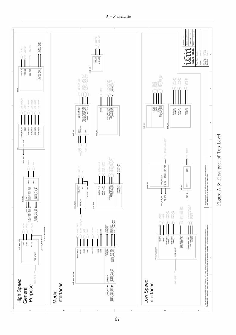
A – Schematic
GB
E1
GB
E0
EN
ET
1_P
HY
_R
ST
EN
ET
0_P
HY
_R
ST
_R
ST
_E
NE
T1_P
HY
_IN
T_E
NE
T0_P
HY
_IN
T
US
B_H
UB
1
US
B_H
UB
2
US
B0
US
B_H
UB
4
US
B_H
UB
3
US
B_H
UB
_S
SH
UB
_R
ST
US
DH
C2
US
DH
C1_V
SE
L
US
DH
C1
US
DH
C2_V
SE
L
_S
D2_R
ST
eth
ern
et
usb
em
mc
Dra
wn b
y:
Checked:
Desig
n b
y:
Pro
ject:
Sheet S
ize:
Page T
itle
:
Sheet:
Date
:
Vers
ion:
CA
D d
raw
ing. F
ree h
and c
hanges a
re n
ot perm
itte
d.
Dis
egno e
seguito s
u C
AD
. N
on s
ono a
mm
esse m
odific
he m
anuali.
This
dra
win
g is a
pro
prieta
ry d
ocum
ent of Id
eas &
Motion s
.r.l. and m
ust not be c
opie
d o
r re
leased to third p
art
ies w
ithout auth
orization.
Questo
dis
egno e
' pro
prieta
' di Id
eas &
Motion s
.r.l. e n
on p
uo' e
ssere
rip
rodotto o
tra
sm
esso a
terz
i senza p
revia
auto
rizzazio
ne.
/A3
12
34
56
78
A B C D E F
Re
vie
we
r
Dra
ftm
an
iMX
8S
OM
L.
Gir
au
di
43
6
1.0
DD
/M
M/
YY
YY
Mo
du
le
_R
ST
QS
PI1
spi_
nor
LC
D1_B
KLT
_E
ND
SI0
_P
WM
_O
UT
LC
D1_V
DD
_E
N
DS
I0
_S
AT
A0_A
CT
imx8_dsi
GB
E1
GB
E0
SA
TA
0
PC
IE1
PC
IE0
SA
TA
0
PC
IE1
PC
IE0
_P
CIE
_W
AK
E_
PC
IE_
WA
KE
LC
D1
_B
KLT_
EN
DS
I0_
PW
M_
OU
TLC
D1
_V
DD
_E
N
DM
A_
I2C
3_
SD
A
DS
I0
US
B0
CS
I1
CS
I_C
AM
_M
CK
GP
IO2/_
CA
M0_R
ST
GP
IO3/_
CA
M1_R
ST
GP
IO1/_
CA
M1_P
WR
GP
IO0/_
CA
M0_P
WR
CS
I0C
SI0
_A
UX
imx8_csi
CS
I1
CS
I_C
AM
_M
CK
CS
I0
US
DH
C2
US
DH
C1
US
DH
C2_V
SE
LU
SD
HC
1_V
SE
L
_S
D2
_R
ST
HD
MI_
TX
DP
HD
MI_
RX
imx8_hdm
i
DP
HD
MI_
TX
DP
0_A
UX
_S
EL
GP
IO4/_
HD
A_R
ST
PG
_1P
2
imx8_adc
LV
DS
1_C
H0
LV
DS
0_C
H0
UA
RT
2_T
XU
AR
T2_R
X
LV
DS
1_C
H1
LV
DS
0_P
WM
0_O
UT
LC
D0_B
KLT
_E
NLC
D0_V
DD
_E
N
LV
DS
0_
CH
0
LV
DS
0_
PW
M0
_O
UT
LC
D0
_V
DD
_E
NLC
D0
_B
KLT_
EN
imx8_lv
ds
SA
I0
SA
I1
SP
I3
AU
DIO
_M
CK
ES
AI1
EN
ET
1_P
HY
_R
ST
EN
ET
0_P
HY
_R
ST
HU
B_R
ST
_E
NE
T1_P
HY
_IN
T_E
NE
T0_P
HY
_IN
T
SP
I2
_W
IFI_
INT
_W
IFI_
RS
TW
IFI_
EN
SP
DIF
0
imx8_esai_
spdi_
spi
SA
I0
SA
I1
QS
PI1
SP
I3
CA
N0
_R
XC
AN
0_
TX
CA
N1
_R
XC
AN
1_
TX
CA
N0_R
XC
AN
0_T
X
CA
N1_R
XC
AN
1_T
X
CA
N2_T
XC
AN
2_R
X
imx8_can
UA
RT
0
UA
RT
1
UA
RT
4_R
XU
AR
T4_T
X
UA
RT
3_T
XU
AR
T3_R
X
DM
A_I2
C2_S
CL
DM
A_I2
C2_S
DA
GP
IO5/P
WM
_O
UT
_S
MB
_A
LE
RT
GP
IO6/T
AC
HIN
GP
IO10
imx8_m
4_gpt_
uart
UA
RT4
_R
XU
AR
T4
_TX
UA
RT3
_TX
UA
RT3
_R
X
UA
RT0
UA
RT1
DM
A_
I2C
2_
SC
LD
MA
_I2
C2
_S
DA
GP
IO5
/P
WM
_O
UT
AU
DIO
_M
CK
GP
IO1
1
GP
IO1
0
GP
IO9
GP
IO8
GP
IO7
GP
IO6
/TA
CH
IN
GP
IO4
/_
HD
A_
RS
T
GP
IO11
GP
IO9
GP
IO8
GP
IO7
DM
A_I2
C3_S
CL
DM
A_I2
C3_S
DA
imx8_sim
CS
I0_
AU
X
MLB
_D
IFF
MLB
_S
E
MLB
_D
IFF
MLB
_S
E
imx8_m
lb
HD
MI_
RX
ES
AI1
CA
N2
_R
XC
AN
2_
TX
_S
MB
_A
LE
RT
_S
AT
A0_A
CT
_R
ST
HU
B_R
ST
EN
ET
0_P
HY
_R
ST
EN
ET
1_P
HY
_R
ST
HU
B_R
ST
EN
ET
0_P
HY
_R
ST
EN
ET
1_P
HY
_R
ST
_E
NE
T0_P
HY
_IN
T_E
NE
T1_P
HY
_IN
T
_E
NE
T0_P
HY
_IN
T_E
NE
T1_P
HY
_IN
T
_S
AT
A0_A
CT
_R
ST
SP
I2
UA
RT
2_T
XU
AR
T2_R
X
WIF
I_E
N_W
IFI_
RS
T_W
IFI_
INT
Hig
h S
peed
Genera
l P
urp
ose
Media
Inte
rfaces
Low
Speed
Inte
rfaces
to G
PIO
in D
SI blo
ck
SP
DIF
0
LV
DS
1_
CH
0LV
DS
1_
CH
1
DM
A_
I2C
3_
SC
L
PG
_1P
2
DP
0_A
UX
_S
EL
DP
0_A
UX
_S
EL
US
B_
HU
B1
US
B_
HU
B2
US
B_
HU
B3
US
B_
HU
B4
US
B_
HU
B_
SS
imx8_pcie
_sata
GP
IO2
/_
CA
M0
_R
ST
GP
IO0
/_
CA
M0
_P
WR
GP
IO3
/_
CA
M1
_R
ST
GP
IO1
/_
CA
M1
_P
WR
Figure
A.3:First
partof
Top
Level
67
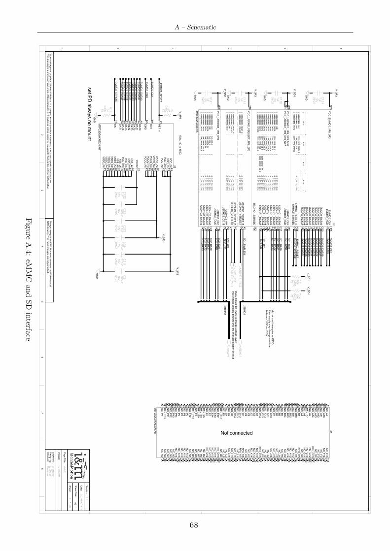
A – Schematic
Dra
wn b
y:
Checked:
Desig
n b
y:
Pro
ject:
Sheet S
ize:
Page T
itle:
Sheet:
Date
:
Vers
ion:
CA
D d
raw
ing. F
ree h
and c
hanges a
re n
ot p
erm
itted.
Dis
egno e
seguito
su C
AD
. Non s
ono a
mm
esse m
odific
he m
anuali.
This
dra
win
g is
a p
roprie
tary
docum
ent o
f Ideas &
Motio
n s
.r.l. and m
ust n
ot b
e c
opie
d o
r rele
ased to
third
partie
s w
ithout a
uth
oriz
atio
n.
Questo
dis
egno e
' pro
prie
ta' d
i Ideas &
Motio
n s
.r.l. e n
on p
uo' e
ssere
ripro
dotto
o tra
sm
esso a
terz
i senza p
revia
auto
rizzazio
ne.
/ A3
12
34
56
78
ABCDEF
Re
vie
we
r
Dra
ftma
n
iMX
8S
OM
L. G
irau
di
53
6
1.0
DD
/M
M/
YY
YY
eM
MC
C3
11
04
02
2.2
uF
10
V
C3
1
04
02
10
0n
F1
6V
C3
12
04
02
2.2
uF
10
V
C3
2
04
02
10
0n
F1
6V
V_3P
3
V_3P
3
US
DH
C2
US
DH
C2
SD
2_D
AT
0S
D2_D
AT
1S
D2_D
AT
2S
D2_D
AT
3
SD
2_C
LK
SD
2_C
MD
_S
D2_C
D
US
DH
C1
SD
1_D
AT
0S
D1_D
AT
1S
D1_D
AT
2S
D1_D
AT
3
SD
1_C
LK
SD
1_C
MD
_S
D1_C
DS
D1_W
P
US
DH
C1
V_3P
3
US
DH
C1
_V
SE
L
C1
20
04
02
1u
F1
0V
GN
D
GN
D
C1
21
04
02
1u
F1
0V
SD
2_W
P
_S
D2
_R
ST
US
DH
C2
_V
SE
L
VS
EL m
akes th
e P
MIC
to c
hange v
olta
ge le
vel:
that v
olta
ge a
ctu
ally
pow
ers
only
the in
terfa
ce s
ectio
n o
f iMX
8
V_S
D1
V_S
D2
C3
31
00
nF
04
02
16
V1
0V
1u
F
04
02
C1
22
C1
23
04
02
1u
F1
0V
10
V1
uF
04
02
C1
24
GN
D
GN
D
R9
04
02
10
K
1% V
_3P
3
SD
1_P
WR
_E
N
EM
MC
0_D
AT
A0
EM
MC
0_D
AT
A1
EM
MC
0_D
AT
A2
EM
MC
0_D
AT
A3
EM
MC
0_D
AT
A4
EM
MC
0_D
AT
A5
EM
MC
0_D
AT
A6
EM
MC
0_D
AT
A7
_E
MM
C0_R
ES
ET
EM
MC
0_S
TR
OB
E
EM
MC
0_C
LK
EM
MC
0_C
MD
_E
MM
C0_R
ES
ET
EM
MC
0_D
AT
A0
EM
MC
0_D
AT
A1
EM
MC
0_D
AT
A2
EM
MC
0_D
AT
A3
EM
MC
0_D
AT
A4
EM
MC
0_D
AT
A5
EM
MC
0_D
AT
A6
EM
MC
0_D
AT
A7
EM
MC
0_C
LK
EM
MC
0_C
MD
EM
MC
0_S
TR
OB
E
GN
D
set P
D a
lways n
o m
ount
V_3P
3GN
D
EM
MC
0_C
LK
EM
MC
0_C
MD
EM
MC
0_D
AT
A0
EM
MC
0_D
AT
A1
EM
MC
0_D
AT
A2
EM
MC
0_D
AT
A3
EM
MC
0_D
AT
A4
EM
MC
0_D
AT
A5
EM
MC
0_D
AT
A6
EM
MC
0_D
AT
A7
EM
MC
0_R
ES
ET
_B
EM
MC
0_S
TR
OB
E
US
DH
C1_C
LK
US
DH
C1_C
MD
US
DH
C1_D
AT
A0
US
DH
C1_D
AT
A1
US
DH
C1_D
AT
A2
US
DH
C1_D
AT
A3
US
DH
C1_D
AT
A4
US
DH
C1_D
AT
A5
US
DH
C1_D
AT
A6
US
DH
C1_D
AT
A7
US
DH
C1_R
ES
ET
_B
US
DH
C1_S
TR
OB
E
US
DH
C1_V
SE
LE
CT
US
DH
C2_C
D_B
US
DH
C2_C
LK
US
DH
C2_C
MD
US
DH
C2_D
AT
A0
US
DH
C2_D
AT
A1
US
DH
C2_D
AT
A2
US
DH
C2_D
AT
A3
US
DH
C2_R
ES
ET
_B
US
DH
C2_V
SE
LE
CT
US
DH
C2_W
P
VD
D_E
MM
C0_1P
8_3P
3
VD
D_U
SD
HC
1_1P
8_3P
3_M
36
VD
D_U
SD
HC
1_1P
8_3P
3_N
37
VD
D_U
SD
HC
2_1P
8_3P
3
VD
D_U
SD
HC
_V
SE
LE
CT
_1P
8_3P
3
+-
--
--
--
--
--
--
--
--
--
--
+-
--
--
--
--
--
--
--
--
--
+-
--
--
--
--
--
--
--
--
-+
--
--
--
--
--
--
--
--
-+
|
A
LT
0
|
AL
T1
|
AL
T2
|
AL
T3
|
+-
--
--
--
--
--
--
--
--
--
--
+-
--
--
--
--
--
--
--
--
--
+-
--
--
--
--
--
--
--
--
-+
--
--
--
--
--
--
--
--
-+
|
CO
NN
_E
MM
C0
_C
LK
|
CO
NN
_N
AN
D_
RE
AD
Y_
B
|
|
|
|
CO
NN
_E
MM
C0
_C
MD
|
CO
NN
_N
AN
D_
DQ
S
|
|
L
SI
O_
GP
IO
5_
IO
03
|
|
CO
NN
_E
MM
C0
_D
AT
A0
|
CO
NN
_N
AN
D_
DA
TA
00
|
CO
NN
_U
SD
HC
1_
CM
D
|
|
|
L
SI
O_
GP
IO
5_
IO
14
|
|
CO
NN
_U
SD
HC
1_
DA
TA
0
|
CO
NN
_N
AN
D_
RE
_N
|
|
L
SI
O_
GP
IO
5_
IO
15
|
|
CO
NN
_U
SD
HC
1_
DA
TA
1
|
CO
NN
_N
AN
D_
RE
_P
|
|
L
SI
O_
GP
IO
5_
IO
16
|
|
CO
NN
_U
SD
HC
1_
DA
TA
2
|
CO
NN
_N
AN
D_
DQ
S_
N
|
|
L
SI
O_
GP
IO
5_
IO
17
|
|
CO
NN
_U
SD
HC
1_
DA
TA
3
|
CO
NN
_N
AN
D_
DQ
S_
P
|
|
L
SI
O_
GP
IO
5_
IO
18
|
|
CO
NN
_U
SD
HC
1_
DA
TA
4
|
CO
NN
_N
AN
D_
CE
0_
B
|
|
L
SI
O_
GP
IO
5_
IO
19
|
|
CO
NN
_U
SD
HC
1_
DA
TA
5
|
CO
NN
_N
AN
D_
RE
_B
|
|
L
SI
O_
GP
IO
5_
IO
20
|
|
CO
NN
_U
SD
HC
1_
DA
TA
6
|
CO
NN
_N
AN
D_
WE
_B
|
CO
NN
_U
SD
HC
1_
WP
|
L
SI
O_
GP
IO
5_
IO
21
|
|
CO
NN
_U
SD
HC
1_
DA
TA
7
|
CO
NN
_N
AN
D_
AL
E
|
CO
NN
_U
SD
HC
1_
CD
_B
|
L
SI
O_
GP
IO
5_
IO
22
|
|
CO
NN
_U
SD
HC
1_
ST
RO
BE
|
CO
NN
_N
AN
D_
CE
1_
B
|
|
L
SI
O_
GP
IO
5_
IO
23
|
|
CO
NN
_U
SD
HC
2_
CL
K
|
AU
D_
MQ
S_
R
|
|
L
SI
O_
GP
IO
5_
IO
24
|
|
CO
NN
_U
SD
HC
2_
CM
D
|
AU
D_
MQ
S_
L
|
|
L
SI
O_
GP
IO
5_
IO
25
|
|
CO
NN
_U
SD
HC
2_
DA
TA
0
|
DM
A_
UA
RT
4_
RX
|
|
L
SI
O_
GP
IO
5_
IO
26
|
|
CO
NN
_U
SD
HC
2_
DA
TA
1
|
DM
A_
UA
RT
4_
TX
|
|
L
SI
O_
GP
IO
5_
IO
27
|
|
CO
NN
_U
SD
HC
2_
DA
TA
2
|
DM
A_
UA
RT
4_
CT
S_
B
|
|
L
SI
O_
GP
IO
5_
IO
28
|
|
CO
NN
_U
SD
HC
2_
DA
TA
3
|
DM
A_
UA
RT
4_
RT
S_
B
|
|
L
SI
O_
GP
IO
5_
IO
29
|
+-
--
--
--
--
--
--
--
--
--
--
+-
--
--
--
--
--
--
--
--
--
+-
--
--
--
--
--
--
--
--
-+
--
--
--
--
--
--
--
--
-+
|
CO
NN
_U
SD
HC
1_
RE
SE
T_
B
|
|
|
L
SI
O_
GP
IO
4_
IO
07
|
|
CO
NN
_U
SD
HC
1_
VS
EL
EC
T
|
|
|
L
SI
O_
GP
IO
4_
IO
08
|
|
CO
NN
_U
SD
HC
2_
RE
SE
T_
B
|
|
|
L
SI
O_
GP
IO
4_
IO
09
|
|
CO
NN
_U
SD
HC
2_
VS
EL
EC
T
|
|
|
L
SI
O_
GP
IO
4_
IO
10
|
|
CO
NN
_U
SD
HC
2_
WP
|
|
|
L
SI
O_
GP
IO
4_
IO
11
|
|
CO
NN
_U
SD
HC
2_
CD
_B
|
|
|
L
SI
O_
GP
IO
4_
IO
12
|
1%
04
02
R1
01
0K
E37
F38
G41
J39
G37
H38
G35
H36
H34
J33
H32
G31
H30
G29
J27
H28
E39
F40
H40
G43
F42
H42
A5
J43
B4
B8
F46
H44
H48
G45
L45
J45
C7
A7
D8
N35
M36
N37
M38
T18
PIM
X8M
6A
VU
DD
1A
U1
do n
ot u
se th
ese p
ins a
s G
PIO
:th
eir s
upply
may c
hange ru
n-tim
ebetw
een 1
.8V
and 3
.3V
R1
1
04
02
10
K
1%
R1
2
04
02
10
K
1%
V_S
D1
V_S
D1
CLK
CM
D
DA
T0
DA
T1
DA
T2
DA
T3
DA
T4
DA
T5
DA
T6
DA
T7
DS
RS
T_n
VC
C_E
6V
CC
_F
5V
CC
_J10
VC
C_K
9
VC
CQ
_C
6V
CC
Q_M
4V
CC
Q_N
4V
CC
Q_P
3V
CC
Q_P
5
VD
DIM
VS
S_A
6V
SS
_E
7V
SS
_G
5V
SS
_H
10
VS
S_J5
VS
S_K
8V
SS
Q_C
4V
SS
Q_N
2V
SS
Q_N
5V
SS
Q_P
4V
SS
Q_P
6
U3
P6
P4
N5
N2
C4
K8
J5
H10
G5
E7
A6
C2
P5
P3
N4
M4
C6
K9
J10
F5
E6
K5
H5
B6
B5
B4
B3
B2
A5
A4
A3
M5
M6
MT
FC
32G
AK
AE
CN
-AIT
Not connected
NC
_A
1N
C_A
10
NC
_A
11
NC
_A
12
NC
_A
13
NC
_A
14
NC
_A
2R
FU
_A
7N
C_A
8N
C_A
9N
C_B
1N
C_B
10
NC
_B
11
NC
_B
12
NC
_B
13
NC
_B
14
NC
_B
7N
C_B
8N
C_B
9N
C_C
1N
C_C
10
NC
_C
11
NC
_C
12
NC
_C
13
NC
_C
14
NC
_C
3N
C_C
5N
C_C
7N
C_C
8N
C_C
9N
C_D
1N
C_D
12
NC
_D
13
NC
_D
14
NC
_D
2N
C_D
3N
C_D
4N
C_E
1R
FU
_E
10
NC
_E
12
NC
_E
13
NC
_E
14
NC
_E
2N
C_E
3R
FU
_E
5R
FU
_E
8R
FU
_E
9N
C_F
1R
FU
_F
10
NC
_F
12
NC
_F
13
NC
_F
14
NC
_F
2N
C_F
3N
C_G
1R
FU
_G
10
NC
_G
12
NC
_G
13
NC
_G
14
NC
_G
2R
FU
_G
3N
C_H
1N
C_H
12
NC
_H
13
NC
_H
14
NC
_H
2N
C_H
3N
C_J1
NC
_J12
NC
_J13
NC
_J14
NC
_J2
NC
_J3
NC
_K
1R
FU
_K
10
NC
_K
12
NC
_K
13
NC
_K
14
NC
_K
2N
C_K
3R
FU
_K
6R
FU
_K
7N
C_L1
NC
_L12
NC
_L13
NC
_L14
NC
_L2
NC
_L3
NC
_M
1N
C_M
10
NC
_M
11
NC
_M
12
NC
_M
13
NC
_M
14
NC
_M
2N
C_M
3N
C_M
7N
C_M
8N
C_M
9N
C_N
1N
C_N
10
NC
_N
11
NC
_N
12
NC
_N
13
NC
_N
14
NC
_N
3N
C_N
6N
C_N
7N
C_N
8N
C_N
9N
C_P
1R
FU
_P
10
NC
_P
11
NC
_P
12
NC
_P
13
NC
_P
14
NC
_P
2N
C_P
7N
C_P
8N
C_P
9
U3
P9
P8
P7
P2
P14
P13
P12
P11
P10
P1
N9
N8
N7
N6
N3
N14
N13
N12
N11
N10
N1
M9
M8
M7
M3
M2
M14
M13
M12
M11
M10
M1
L3
L2
L14
L13
L12
L1
K7
K6
K3
K2
K14
K13
K12
K10
K1
J3
J2
J14
J13
J12
J1
H3
H2
H14
H13
H12
H1
G3
G2
G14
G13
G12
G10
G1
F3
F2
F14
F13
F12
F10
F1
E9
E8
E5
E3
E2
E14
E13
E12
E10
E1
D4
D3
D2
D14
D13
D12
D1
C9
C8
C7
C5
C3
C14
C13
C12
C11
C10
C1
B9
B8
B7
B14
B13
B12
B11
B10
B1
A9
A8
A7
A2
A14
A13
A12
A11
A10
A1
MT
FC
32G
AK
AE
CN
-AIT
153p, -4
0 to
105C
Figu
reA.4:
eMMC
andSD
interface
68
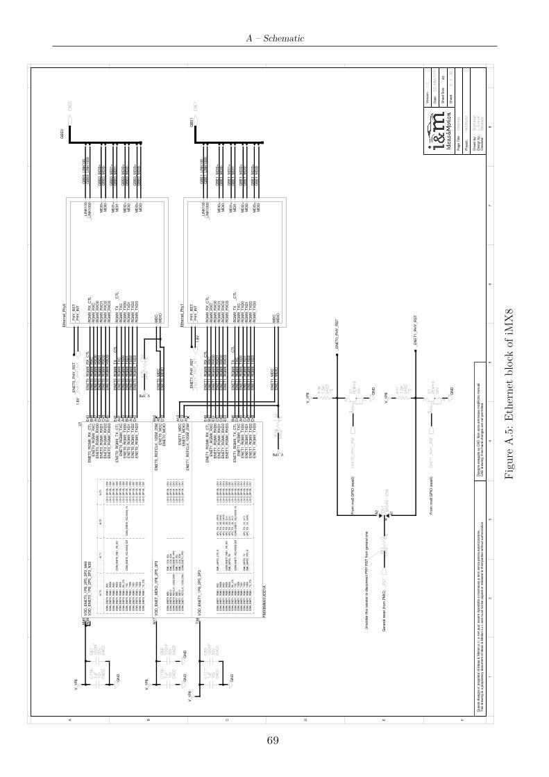
A – Schematic
EN
ET
0_M
DC
EN
ET
0_M
DIO
EN
ET
0_R
EF
CLK
_125M
_25M
EN
ET
0_R
GM
II_R
X_C
TL
EN
ET
0_R
GM
II_R
XC
EN
ET
0_R
GM
II_R
XD
0E
NE
T0_R
GM
II_R
XD
1E
NE
T0_R
GM
II_R
XD
2E
NE
T0_R
GM
II_R
XD
3
EN
ET
0_R
GM
II_T
X_C
TL
EN
ET
0_R
GM
II_T
XC
EN
ET
0_R
GM
II_T
XD
0E
NE
T0_R
GM
II_T
XD
1E
NE
T0_R
GM
II_T
XD
2E
NE
T0_R
GM
II_T
XD
3
EN
ET
1_M
DC
EN
ET
1_M
DIO
EN
ET
1_R
EF
CLK
_125M
_25M
EN
ET
1_R
GM
II_R
X_C
TL
EN
ET
1_R
GM
II_R
XC
EN
ET
1_R
GM
II_R
XD
0E
NE
T1_R
GM
II_R
XD
1E
NE
T1_R
GM
II_R
XD
2E
NE
T1_R
GM
II_R
XD
3
EN
ET
1_R
GM
II_T
X_C
TL
EN
ET
1_R
GM
II_T
XC
EN
ET
1_R
GM
II_T
XD
0E
NE
T1_R
GM
II_T
XD
1E
NE
T1_R
GM
II_T
XD
2E
NE
T1_R
GM
II_T
XD
3
VD
D_E
NE
T0_1P
8_2P
5_3P
3_M
40
VD
D_E
NE
T_M
DIO
_1P
8_2P
5_3P
3
VD
D_E
NE
T1_1P
8_2P
5_3P
3
VD
D_E
NE
T0_1P
8_2P
5_3P
3_N
39
+-
--
--
--
--
--
--
--
--
--
--
--
--
--
-+
--
--
--
--
--
--
--
--
--
--
--
--
+-
--
--
--
--
--
--
--
--
--
--
--
+-
--
--
--
--
--
--
--
--
+
|
A
LT
0
|
AL
T1
|
AL
T2
|
A
LT
3
|
+-
--
--
--
--
--
--
--
--
--
--
--
--
--
-+
--
--
--
--
--
--
--
--
--
--
--
--
+-
--
--
--
--
--
--
--
--
--
--
--
+-
--
--
--
--
--
--
--
--
+
|
CO
NN
_E
NE
T0
_R
GM
II
_R
XC
|
|
|
LS
IO
_G
PI
O6
_I
O0
4
|
|
CO
NN
_E
NE
T0
_R
GM
II
_R
XD
0
|
|
|
LS
IO
_G
PI
O6
_I
O0
6
|
|
CO
NN
_E
NE
T0
_R
GM
II
_R
XD
1
|
|
|
LS
IO
_G
PI
O6
_I
O0
7
|
|
CO
NN
_E
NE
T0
_R
GM
II
_R
XD
2
|
C
ON
N_
EN
ET
0_
RM
II
_R
X_
ER
|
|
LS
IO
_G
PI
O6
_I
O0
8
|
|
CO
NN
_E
NE
T0
_R
GM
II
_R
XD
3
|
|
|
LS
IO
_G
PI
O6
_I
O0
9
|
|
CO
NN
_E
NE
T0
_R
GM
II
_R
X_
CT
L
|
|
|
LS
IO
_G
PI
O6
_I
O0
5
|
|
CO
NN
_E
NE
T0
_R
GM
II
_T
XC
|
C
ON
N_
EN
ET
0_
RC
LK
50
M_
OU
T
|
CO
NN
_E
NE
T0
_R
CL
K5
0M
_I
N
|
LS
IO
_G
PI
O5
_I
O3
0
|
|
CO
NN
_E
NE
T0
_R
GM
II
_T
XD
0
|
|
|
LS
IO
_G
PI
O6
_I
O0
0
|
|
CO
NN
_E
NE
T0
_R
GM
II
_T
XD
1
|
|
|
LS
IO
_G
PI
O6
_I
O0
1
|
|
CO
NN
_E
NE
T0
_R
GM
II
_T
XD
2
|
|
|
LS
IO
_G
PI
O6
_I
O0
2
|
|
CO
NN
_E
NE
T0
_R
GM
II
_T
XD
3
|
|
|
LS
IO
_G
PI
O6
_I
O0
3
|
|
CO
NN
_E
NE
T0
_R
GM
II
_T
X_
CT
L
|
|
|
LS
IO
_G
PI
O5
_I
O3
1
|
|
CO
NN
_E
NE
T0
_M
DC
|
D
MA
_I
2C
4_
SC
L
|
|
LS
IO
_G
PI
O4
_I
O1
4
|
|
CO
NN
_E
NE
T0
_M
DI
O
|
D
MA
_I
2C
4_
SD
A
|
|
LS
IO
_G
PI
O4
_I
O1
3
|
|
CO
NN
_E
NE
T0
_R
EF
CL
K_
12
5M
_2
5M
|
C
ON
N_
EN
ET
0_
PP
S
|
|
LS
IO
_G
PI
O4
_I
O1
5
|
|
CO
NN
_E
NE
T1
_M
DC
|
D
MA
_I
2C
4_
SC
L
|
|
LS
IO
_G
PI
O4
_I
O1
8
|
|
CO
NN
_E
NE
T1
_M
DI
O
|
D
MA
_I
2C
4_
SD
A
|
|
LS
IO
_G
PI
O4
_I
O1
7
|
|
CO
NN
_E
NE
T1
_R
EF
CL
K_
12
5M
_2
5M
|
C
ON
N_
EN
ET
1_
PP
S
|
|
LS
IO
_G
PI
O4
_I
O1
6
|
|
CO
NN
_E
NE
T1
_R
GM
II
_R
XC
|
D
MA
_U
AR
T3
_C
TS
_B
|
VP
U_
TS
I_
S1
_D
AT
A
|
LS
IO
_G
PI
O6
_I
O1
6
|
|
CO
NN
_E
NE
T1
_R
GM
II
_R
XD
0
|
|
VP
U_
TS
I_
S0
_S
YN
C
|
LS
IO
_G
PI
O6
_I
O1
8
|
|
CO
NN
_E
NE
T1
_R
GM
II
_R
XD
1
|
|
VP
U_
TS
I_
S0
_D
AT
A
|
LS
IO
_G
PI
O6
_I
O1
9
|
|
CO
NN
_E
NE
T1
_R
GM
II
_R
XD
2
|
C
ON
N_
EN
ET
1_
RM
II
_R
X_
ER
|
VP
U_
TS
I_
S0
_C
LK
|
LS
IO
_G
PI
O6
_I
O2
0
|
|
CO
NN
_E
NE
T1
_R
GM
II
_R
XD
3
|
D
MA
_U
AR
T3
_R
X
|
VP
U_
TS
I_
S1
_C
LK
|
LS
IO
_G
PI
O6
_I
O2
1
|
|
CO
NN
_E
NE
T1
_R
GM
II
_R
X_
CT
L
|
|
VP
U_
TS
I_
S0
_V
ID
|
LS
IO
_G
PI
O6
_I
O1
7
|
|
CO
NN
_E
NE
T1
_R
GM
II
_T
XC
|
C
ON
N_
EN
ET
1_
RC
LK
50
M_
OU
T
|
CO
NN
_E
NE
T1
_R
CL
K5
0M
_I
N
|
LS
IO
_G
PI
O6
_I
O1
0
|
|
CO
NN
_E
NE
T1
_R
GM
II
_T
XD
0
|
|
|
LS
IO
_G
PI
O6
_I
O1
2
|
|
CO
NN
_E
NE
T1
_R
GM
II
_T
XD
1
|
|
|
LS
IO
_G
PI
O6
_I
O1
3
|
|
CO
NN
_E
NE
T1
_R
GM
II
_T
XD
2
|
D
MA
_U
AR
T3
_T
X
|
VP
U_
TS
I_
S1
_V
ID
|
LS
IO
_G
PI
O6
_I
O1
4
|
|
CO
NN
_E
NE
T1
_R
GM
II
_T
XD
3
|
D
MA
_U
AR
T3
_R
TS
_B
|
VP
U_
TS
I_
S1
_S
YN
C
|
LS
IO
_G
PI
O6
_I
O1
5
|
|
CO
NN
_E
NE
T1
_R
GM
II
_T
X_
CT
L
|
|
|
LS
IO
_G
PI
O6
_I
O1
1
|
+-
--
--
--
--
--
--
--
--
--
--
--
--
--
-+
--
--
--
--
--
--
--
--
--
--
--
--
+-
--
--
--
--
--
--
--
--
--
--
--
+-
--
--
--
--
--
--
--
--
+
Dra
wn b
y:
Checked:
Desig
n b
y:
Pro
ject:
Sheet S
ize:
Page T
itle
:
Sheet:
Date
:
Vers
ion:
CA
D d
raw
ing. F
ree h
and c
hanges a
re n
ot perm
itte
d.
Dis
egno e
seguito s
u C
AD
. N
on s
ono a
mm
esse m
odific
he m
anuali.
This
dra
win
g is a
pro
prieta
ry d
ocum
ent of Id
eas &
Motion s
.r.l. and m
ust not be c
opie
d o
r re
leased to third p
art
ies w
ithout auth
orization.
Questo
dis
egno e
' pro
prieta
' di Id
eas &
Motion s
.r.l. e n
on p
uo' e
ssere
rip
rodotto o
tra
sm
esso a
terz
i senza p
revia
auto
rizzazio
ne.
/A3
12
34
56
78
A B C D E F
GN
D
EN
ET
0_R
GM
II_R
X_C
TL
EN
ET
0_R
GM
II_R
XC
EN
ET
0_R
GM
II_R
XD
0E
NE
T0_R
GM
II_R
XD
1E
NE
T0_R
GM
II_R
XD
2E
NE
T0_R
GM
II_R
XD
3
EN
ET
0_R
GM
II_T
X
_C
TL
EN
ET
0_R
GM
II_T
XC
EN
ET
0_R
GM
II_T
XD
0E
NE
T0_R
GM
II_T
XD
1E
NE
T0_R
GM
II_T
XD
2E
NE
T0_R
GM
II_T
XD
3
EN
ET
0_M
DC
EN
ET
0_M
DIO
RG
MII_T
XD
3R
GM
II_T
XD
2R
GM
II_T
XD
1R
GM
II_T
XD
0R
GM
II_T
XC
RG
MII_T
X
_C
TL
RG
MII_R
XD
3R
GM
II_R
XD
2
RG
MII_R
XD
0R
GM
II_R
XD
1
RG
MII_R
XC
RG
MII_R
X_C
TL
MD
IOM
DC
_P
HY
_R
ST
_P
HY
_IN
T
_LIN
K100
_LIN
K1000
MD
I0+
MD
I0-
MD
I1+
MD
I1-
MD
I2+
MD
I2-
MD
I3+
MD
I3-
GB
E0
_E
NE
T0_P
HY
_R
ST
EN
ET
1_R
GM
II_R
X_C
TL
EN
ET
1_R
GM
II_R
XC
EN
ET
1_R
GM
II_R
XD
1E
NE
T1_R
GM
II_R
XD
0
EN
ET
1_R
GM
II_R
XD
2E
NE
T1_R
GM
II_R
XD
3
EN
ET
1_R
GM
II_T
X
_C
TL
EN
ET
1_R
GM
II_T
XC
EN
ET
1_R
GM
II_T
XD
0E
NE
T1_R
GM
II_T
XD
1E
NE
T1_R
GM
II_T
XD
2E
NE
T1_R
GM
II_T
XD
3
GB
E1
EN
ET
1_M
DC
EN
ET
1_M
DIO
_E
NE
T1_P
HY
_R
ST
GN
D
GN
D
Genera
l re
set (f
rom
PM
IC)
Fro
m im
x8 G
PIO
(esai0
)
Fro
m im
x8 G
PIO
(esai0
)
Unsold
er
this
resis
tor
to d
isconnect P
HY
RS
T fro
m g
enera
l one
GN
D
1.8
V
1.8
V
_E
NE
T0_P
HY
_R
ST
_E
NE
T1_P
HY
_R
ST
_G
BE
0_LIN
K100
_G
BE
0_LIN
K1000
GB
E0_M
DI0
+G
BE
0_M
DI0
-
GB
E0_M
DI1
+G
BE
0_M
DI1
-
GB
E0_M
DI2
+G
BE
0_M
DI2
-
GB
E0_M
DI3
+G
BE
0_M
DI3
-
RG
MII_T
XD
3R
GM
II_T
XD
2R
GM
II_T
XD
1R
GM
II_T
XD
0R
GM
II_T
XC
RG
MII_T
X
_C
TL
RG
MII_R
XD
3R
GM
II_R
XD
2
RG
MII_R
XD
0R
GM
II_R
XD
1
RG
MII_R
XC
RG
MII_R
X_C
TL
MD
IOM
DC
_P
HY
_R
ST
_P
HY
_IN
T
_LIN
K100
_LIN
K1000
MD
I0+
MD
I0-
MD
I1+
MD
I1-
MD
I2+
MD
I2-
MD
I3+
MD
I3-
_G
BE
1_LIN
K100
_G
BE
1_LIN
K1000
GB
E1_M
DI0
+G
BE
1_M
DI0
-
GB
E1_M
DI1
+G
BE
1_M
DI1
-
GB
E1_M
DI2
+G
BE
1_M
DI2
-
GB
E1_M
DI3
+G
BE
1_M
DI3
-
U1
PIM
X8M
6A
VU
DD
1A
N39
T38
N17
M40
D48
G47
C47
A49
D46
B48
E53
D52
C51
E51
B50
E49
A11
C13
A13
D42
A45
B42
A43
A41
E41
E45
C45
D44
A47
B44
E43
B10
D10
A9
V_1P
8
Re
vie
we
r
Dra
ftm
an
iMX
8S
OM
L.
Gir
au
di
63
6
1.0
DD
/M
M/
YY
YY
Eth
ern
et
GB
E1
GB
E0
V_1P
8
_R
ST
V_1P
8
C8
5
04
02
10
0n
F5
0V
C1
17
04
02
1u
F1
0V
V_1P
8
V_1P
8
C8
6
04
02
10
0n
F5
0V
V_1P8
EN
ET1
_P
HY
_R
ST
EN
ET0
_P
HY
_R
ST
_E
NE
T1
_P
HY
_IN
T
_E
NE
T0
_P
HY
_IN
T
R8
10
40
20 1
%
C8
7
04
02
10
0n
F5
0V
1%
1.5
K0
40
2R
76
10
V1
uF
04
02
C1
18
V_1P8
10
V1
uF
04
02
C1
16
Eth
ern
et_
Phy1
1%
1.5
K0
40
2R
75
Eth
ern
et_
Phy0
04
02
R7
7
1%
1.5
K
04
02
R7
8
1%
1.5
K
Q1
43
5P
EM
H9
50
V
GN
D
GN
D
Q1
16
2P
EM
H9
50
V
K
A1A2 DS
1B
AS
40
-0
5W
Figure
A.5:Ethernet
block
ofiM
X8
69
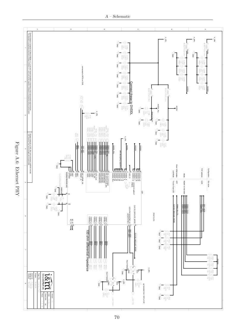
A – Schematic
TX
RX
M_A
TX
RX
M_B
TX
RX
M_C
TX
RX
M_D
TX
RX
P_A
TX
RX
P_B
TX
RX
P_C
TX
RX
P_D
CLK
125_N
DO
/LE
D_M
OD
E
LE
D1/P
HY
AD
0/P
ME
_N
1LE
D2/P
HY
AD
1
EP
GN
D
AV
DD
H_1
AV
DD
H_12
DV
DD
H_40
DV
DD
H_34
DV
DD
H_16
AV
DD
L_4
AV
DD
L_9
DV
DD
L_18
DV
DD
L_14
DV
DD
L_39
DV
DD
L_30
DV
DD
L_26
DV
DD
L_23
LD
O_O
RX
_C
LK
/PH
YA
D2
RX
_D
V/C
LK
125_E
NR
XD
0/M
OD
E0
RX
D1/M
OD
E1
RX
D2/M
OD
E2
RX
D3/M
OD
E3
TX
_E
NT
XD
0T
XD
1T
XD
2T
XD
3
MD
CM
DIO
GT
X_C
LK
NC
_13
NC
_47
VS
S
XI
XO
AV
DD
L_P
LL
INT
_N
/PM
E_N
2
ISE
T
RE
SE
T_N
connect to
gate
of
PM
OS
GN
D
GN
D
GN
D
GN
D
GN
D
GN
D
GN
DG
ND
GN
DG
ND
GN
DG
ND
GN
D
GN
DG
ND
GN
DG
ND
GN
D
Ferrite
Ferrite
connecte
d to
GP
T0 o
n E
VB
clo
se to
pin
sclo
se to
the p
in
PH
Y a
ddre
ss
Mode
Clo
ck 1
25M
enable
Led M
ode
MD
I0+
MD
I0-
MD
I1+
MD
I1-
MD
I2+
MD
I2-
MD
I3+
MD
I3-
DV
DD
H
AV
DD
H
DV
DD
H
AV
DD
H
RG
MII_
RX
_C
TL
RG
MII_
RX
C
RG
MII_
RX
D1
RG
MII_
RX
D0
RG
MII_
RX
D2
RG
MII_
RX
D3
RG
MII_
TX
_C
TL
RG
MII_
TX
C
RG
MII_
TX
D0
RG
MII_
TX
D1
RG
MII_
TX
D2
RG
MII_
TX
D3
MD
CM
DIO
CLK
125_N
DO
/LE
D_M
OD
E
AV
DD
L_P
LL
PH
Y_LE
D0
DV
DD
H
PH
Y_LE
D0
PH
Y_LE
D1
RG
MII_
RX
C
RG
MII_
RX
D0
RG
MII_
RX
D1
RG
MII_
RX
D2
RG
MII_
RX
D3
RG
MII_
RX
_C
TL
CLK
125_N
DO
/LE
D_M
OD
E
Dra
wn b
y:
Checked:
Desig
n b
y:
Pro
ject:
Sheet S
ize:
Page T
itle:
Sheet:
Date
:
Vers
ion:
CA
D d
raw
ing. F
ree h
and c
hanges a
re n
ot p
erm
itted.
Dis
egno e
seguito
su C
AD
. Non s
ono a
mm
esse m
odific
he m
anuali.
This
dra
win
g is
a p
roprie
tary
docum
ent o
f Ideas &
Motio
n s
.r.l. and m
ust n
ot b
e c
opie
d o
r rele
ased to
third
partie
s w
ithout a
uth
oriz
atio
n.
Questo
dis
egno e
' pro
prie
ta' d
i Ideas &
Motio
n s
.r.l. e n
on p
uo' e
ssere
ripro
dotto
o tra
sm
esso a
terz
i senza p
revia
auto
rizzazio
ne.
/ A3
12
34
56
78
ABCDEF
_P
HY
_IN
T_P
HY
_R
ST
GN
DG
ND
GN
D
GN
D
PH
Y_LE
D1
up tra
nsla
te fro
m 1
.8V
to 3
.3V
100 o
hm
diffe
rentia
l impedance
Config
ura
tion
Set v
alu
e
OF
F
Tric
olo
r Dual-L
ED
0x00
RG
MII 1
0/1
00/1
000
34
1649
18
36
14
39
811
25
30
26
710
41
17
23
49
15
112
40
43
35
33
32
31
28
27
25
19
20
21
22
36
37
24
13
47
29
46
45
44
38
48
42
U24
KS
Z9031R
NX
VB
-VA
O
C3
46
04
02
10
nF
50
V
C3
47
50
V1
0n
F
04
02
50
V
C3
48
04
02
10
nF
C3
94
08
05
10
uF
10
V
L5BLM
21
PG
22
1S
N1
50
V1
0n
F
04
02
C3
49
C3
50
04
02
10
nF
50
V
C3
95
08
05
10
uF
10
V
L6BLM
21
PG
22
1S
N1
V_1P
2
V_1P
8
10
V1
0u
FC
39
6
08
05
BLM
21
PG
22
1S
N1
0H
L7BLM
21
PG
22
1S
N1
L8
0H
C3
97
10
uF
08
05
10
V
C1
00
04
02
10
0n
F5
0V
50
V1
00
nF
04
02
C1
01
C1
02
04
02
10
0n
F5
0V
50
V1
00
nF
04
02
C1
03
C1
04
04
02
10
0n
F5
0V
50
V1
00
nF
04
02
C1
05
1K
1%
R4
1
04
02
1K
1%
R4
2
04
02
04
02
R4
3
1%
1K
04
02
R4
4
1%
1K
04
02
R4
5
1%
1K
Dra
ftma
n
Re
vie
we
rL
. Gira
ud
i
iMX
8S
OM
36
7
DD
/M
M/
YY
YY
1.0
Eth
ern
et_
Ph
y0
MD
C
RG
MII_
RX
_C
TL
RG
MII_
RX
C
RG
MII_
RX
D1
RG
MII_
RX
D0
RG
MII_
RX
D2
RG
MII_
RX
D3
RG
MII_
TX
_C
TL
RG
MII_
TX
C
RG
MII_
TX
D0
RG
MII_
TX
D1
RG
MII_
TX
D2
RG
MII_
TX
D3
MD
IO
Y2
CX
32
25
SA
25
00
0D
0P
TV
CC
25M
EG
Hz
04
02
R2
8
1%
10
K0
40
2
R2
9
1%
10
K0
40
2
R3
0
1%
10
K0
40
2
R3
1
1%
10
K
Connect th
ese to
DV
DD
L
AV
DD
L
AV
DD
L_P
LL
C1
98
04
02
1u
F1
0V
C3
51
04
02
10
nF
50
V
GN
DG
ND
C1
06
04
02
10
0n
F5
0V
C1
07
04
02
10
0n
F5
0VA
VD
DL
with
decouplin
g c
apacito
rs
C4
04
04
02
15
pF
50
V5
0V
15
pF
04
02
C4
05
V_1P
2
V_3P
3
V_1P
8
MD
I3-
MD
I3+
MD
I2-
MD
I2+
MD
I1-
MD
I1+
MD
I0-
MD
I0+
_LIN
K1
00
0
_LIN
K1
00
_P
HY
_R
ST
_P
HY
_IN
T
04
02
R7
9
1%
1.5
K
AY VC
C
GN
D
24
5
3
74LV
1T
34G
W
U7
AY VC
C
GN
D
24
5
3
74LV
1T
34G
W
U8
R1
59
04
02
12
.1K
1%
GN
D
GN
D
V_3P
3
V_3P
3 C?
04
02
22
0n
F1
6V
16
V2
20
nF
04
02
C?
Figu
reA.6:
Ethern
etPHY
70

A – Schematic
AD
C_IN
0A
DC
_IN
1A
DC
_IN
2A
DC
_IN
3
AD
C_IN
4A
DC
_IN
5A
DC
_IN
6A
DC
_IN
7
VD
D_A
DC
_1P
8V
DD
_A
DC
_D
IG_1P
8
VR
EF
L_A
DC
VR
EF
H_A
DC
AN
A_T
ES
T_O
UT
0_N
AN
A_T
ES
T_O
UT
0_P
AN
A_T
ES
T_O
UT
1_N
AN
A_T
ES
T_O
UT
1_P
+-
--
--
--
--
--
--
+-
--
--
--
--
--
--
-+
--
--
--
--
--
--
--
--
+-
--
--
--
--
--
--
--
--
+
|
A
LT
0
|
AL
T1
|
AL
T2
|
A
LT
3
|
+-
--
--
--
--
--
--
+-
--
--
--
--
--
--
-+
--
--
--
--
--
--
--
--
+-
--
--
--
--
--
--
--
--
+
|
DM
A_
AD
C_
IN
0
|
|
L
SI
O_
KP
P0
_C
OL
0
|
LS
IO
_G
PI
O3
_I
O1
8
|
|
DM
A_
AD
C_
IN
1
|
|
L
SI
O_
KP
P0
_C
OL
1
|
LS
IO
_G
PI
O3
_I
O1
9
|
|
DM
A_
AD
C_
IN
2
|
|
L
SI
O_
KP
P0
_C
OL
2
|
LS
IO
_G
PI
O3
_I
O2
0
|
|
DM
A_
AD
C_
IN
3
|
DM
A_
SP
I1
_S
CK
|
L
SI
O_
KP
P0
_C
OL
3
|
LS
IO
_G
PI
O3
_I
O2
1
|
|
DM
A_
AD
C_
IN
4
|
DM
A_
SP
I1
_S
DO
|
L
SI
O_
KP
P0
_R
OW
0
|
LS
IO
_G
PI
O3
_I
O2
2
|
|
DM
A_
AD
C_
IN
5
|
DM
A_
SP
I1
_S
DI
|
L
SI
O_
KP
P0
_R
OW
1
|
LS
IO
_G
PI
O3
_I
O2
3
|
|
DM
A_
AD
C_
IN
6
|
DM
A_
SP
I1
_C
S0
|
L
SI
O_
KP
P0
_R
OW
2
|
LS
IO
_G
PI
O3
_I
O2
4
|
|
DM
A_
AD
C_
IN
7
|
DM
A_
SP
I1
_C
S1
|
L
SI
O_
KP
P0
_R
OW
3
|
LS
IO
_G
PI
O3
_I
O2
5
|
+-
--
--
--
--
--
--
+-
--
--
--
--
--
--
-+
--
--
--
--
--
--
--
--
+-
--
--
--
--
--
--
--
--
+
DP
0_
AU
X_
SE
L
V_1P
8
GN
D
Dra
wn b
y:
Checked:
Desig
n b
y:
Pro
ject:
Sheet S
ize:
Page T
itle
:
Date
:
Vers
ion:
CA
D d
raw
ing. F
ree h
and c
hanges a
re n
ot perm
itte
d.
Dis
egno e
seguito s
u C
AD
. N
on s
ono a
mm
esse m
odific
he m
anuali.
This
dra
win
g is a
pro
prieta
ry d
ocum
ent of Id
eas &
Motion s
.r.l. and m
ust not be c
opie
d o
r re
leased to third p
art
ies w
ithout auth
orization.
Questo
dis
egno e
' pro
prieta
' di Id
eas &
Motion s
.r.l. e n
on p
uo' e
ssere
rip
rodotto o
tra
sm
esso a
terz
i senza p
revia
auto
rizzazio
ne.
Sheet:
/A4
Re
vie
we
r
L.
Gir
au
di
iMX
8S
OM
Dra
ftm
an
93
6
1.0
DD
/M
M/
YY
YY
imx
8_
ad
c
U1
PIM
X8M
6A
VU
DD
1A
AP
6A
L9
AR
7A
N9
AR
9A
P8
AN
11
AP
10
BE
1B
D2
BG
53
BH
52
AL11
AM
10
AK
16
AL15
V_1P
8_F
ILT
ER
C1
33
04
02
1u
F1
0V
PG
_1
P2
Inte
rnal pull
dow
n e
nable
d b
y d
efa
ult
GP
IO4
/_
HD
A_
RS
T
Figure
A.7:ADC
Block
ofiM
X8
71

A – Schematic
FLE
XC
AN
0_R
XF
LE
XC
AN
0_T
X
FLE
XC
AN
1_R
XF
LE
XC
AN
1_T
X
FLE
XC
AN
2_R
XF
LE
XC
AN
2_T
X
VD
D_F
LE
XC
AN
_1P
8_3P
3
+-
--
--
--
--
--
--
--
--
+-
--
--
-+
--
--
--
+-
--
--
--
--
--
--
--
--
+
|
A
LT
0
|
AL
T1
|
A
LT
2
|
A
LT
3
|
+-
--
--
--
--
--
--
--
--
+-
--
--
-+
--
--
--
+-
--
--
--
--
--
--
--
--
+
|
DM
A_
FL
EX
CA
N0
_R
X
|
|
|
LS
IO
_G
PI
O3
_I
O2
9
|
|
DM
A_
FL
EX
CA
N0
_T
X
|
|
|
LS
IO
_G
PI
O3
_I
O3
0
|
|
DM
A_
FL
EX
CA
N1
_R
X
|
|
|
LS
IO
_G
PI
O3
_I
O3
1
|
|
DM
A_
FL
EX
CA
N1
_T
X
|
|
|
LS
IO
_G
PI
O4
_I
O0
0
|
|
DM
A_
FL
EX
CA
N2
_R
X
|
|
|
LS
IO
_G
PI
O4
_I
O0
1
|
|
DM
A_
FL
EX
CA
N2
_T
X
|
|
|
LS
IO
_G
PI
O4
_I
O0
2
|
+-
--
--
--
--
--
--
--
--
+-
--
--
-+
--
--
--
+-
--
--
--
--
--
--
--
--
+
U1
N15
E7
C3
G7
E5
H6
PIM
X8M
6A
VU
DD
1A
V_1P
8
CA
N1
_TX
CA
N1
_R
X
CA
N0
_TX
CA
N0
_R
X
CA
N1_T
XC
AN
1_R
X
CA
N0_T
XC
AN
0_R
X
Dra
wn b
y:
Checked:
Desig
n b
y:
Pro
ject:
Sheet S
ize:
Page T
itle:
Date
:
Vers
ion:
CA
D d
raw
ing. F
ree h
and c
hanges a
re n
ot p
erm
itted.
Dis
egno e
seguito
su C
AD
. Non s
ono a
mm
esse m
odific
he m
anuali.
This
dra
win
g is
a p
roprie
tary
docum
ent o
f Ideas &
Motio
n s
.r.l. and m
ust n
ot b
e c
opie
d o
r rele
ased to
third
partie
s w
ithout a
uth
oriz
atio
n.
Questo
dis
egno e
' pro
prie
ta' d
i Ideas &
Motio
n s
.r.l. e n
on p
uo' e
ssere
ripro
dotto
o tra
sm
esso a
terz
i senza p
revia
auto
rizzazio
ne.
Sheet:
/ A4
Re
vie
we
r
Dra
ftma
n
iMX
8S
OM
L. G
irau
di
10
36
1.0
DD
/M
M/
YY
YY
imx
8_
ca
n
CA
N2
_R
XC
AN
2_
TX
CA
N2_R
XC
AN
2_T
X
C5
GN
D
10
V
C1
37
04
02
1u
F
Figu
reA.8:
Can
Block
ofiM
X8
72
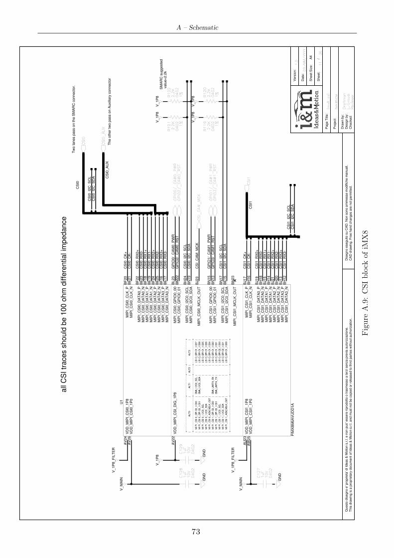
A – Schematic
Dra
wn b
y:
Checked:
Desig
n b
y:
Pro
ject:
Sheet S
ize:
Page T
itle
:
Date
:
Vers
ion:
CA
D d
raw
ing. F
ree h
and c
hanges a
re n
ot perm
itte
d.
Dis
egno e
seguito s
u C
AD
. N
on s
ono a
mm
esse m
odific
he m
anuali.
This
dra
win
g is a
pro
prieta
ry d
ocum
ent of Id
eas &
Motion s
.r.l. and m
ust not be c
opie
d o
r re
leased to third p
art
ies w
ithout auth
orization.
Questo
dis
egno e
' pro
prieta
' di Id
eas &
Motion s
.r.l. e n
on p
uo' e
ssere
rip
rodotto o
tra
sm
esso a
terz
i senza p
revia
auto
rizzazio
ne.
Sheet:
/A4
CS
I1
MIP
I_C
SI0
_C
LK
_N
MIP
I_C
SI0
_C
LK
_P
MIP
I_C
SI0
_D
AT
A0_N
MIP
I_C
SI0
_D
AT
A0_P
MIP
I_C
SI0
_D
AT
A1_N
MIP
I_C
SI0
_D
AT
A1_P
MIP
I_C
SI0
_D
AT
A2_N
MIP
I_C
SI0
_D
AT
A2_P
MIP
I_C
SI0
_D
AT
A3_N
MIP
I_C
SI0
_D
AT
A3_P
MIP
I_C
SI0
_G
PIO
0_00
MIP
I_C
SI0
_G
PIO
0_01
MIP
I_C
SI0
_I2
C0_S
CL
MIP
I_C
SI0
_I2
C0_S
DA
MIP
I_C
SI0
_M
CLK
_O
UT
MIP
I_C
SI1
_C
LK
_N
MIP
I_C
SI1
_C
LK
_P
MIP
I_C
SI1
_D
AT
A0_N
MIP
I_C
SI1
_D
AT
A0_P
MIP
I_C
SI1
_D
AT
A1_N
MIP
I_C
SI1
_D
AT
A1_P
MIP
I_C
SI1
_D
AT
A2_N
MIP
I_C
SI1
_D
AT
A2_P
MIP
I_C
SI1
_D
AT
A3_N
MIP
I_C
SI1
_D
AT
A3_P
MIP
I_C
SI1
_G
PIO
0_00
MIP
I_C
SI1
_G
PIO
0_01
MIP
I_C
SI1
_I2
C0_S
CL
MIP
I_C
SI1
_I2
C0_S
DA
MIP
I_C
SI1
_M
CLK
_O
UT
VD
D_M
IPI_
CS
I0_1P
0V
DD
_M
IPI_
CS
I0_1P
8
VD
D_M
IPI_
CS
I1_1P
0V
DD
_M
IPI_
CS
I1_1P
8
VD
D_M
IPI_
CS
I_D
IG_1P
8
+-
--
--
--
--
--
--
--
--
--
--
--
-+
--
--
--
--
--
--
--
+-
--
--
-+
--
--
--
--
--
--
--
--
-+
|
A
LT
0
|
A
LT
1
|
AL
T2
|
AL
T3
|
+-
--
--
--
--
--
--
--
--
--
--
--
-+
--
--
--
--
--
--
--
+-
--
--
-+
--
--
--
--
--
--
--
--
-+
|
MI
PI
_C
SI
0_
GP
IO
0_
IO
00
|
D
MA
_I
2C
0_
SC
L
|
|
L
SI
O_
GP
IO
1_
IO
27
|
|
MI
PI
_C
SI
0_
GP
IO
0_
IO
01
|
D
MA
_I
2C
0_
SD
A
|
|
L
SI
O_
GP
IO
1_
IO
28
|
|
MI
PI
_C
SI
0_
I2
C0
_S
CL
|
|
|
L
SI
O_
GP
IO
1_
IO
25
|
|
MI
PI
_C
SI
0_
I2
C0
_S
DA
|
|
|
L
SI
O_
GP
IO
1_
IO
26
|
|
MI
PI
_C
SI
0_
AC
M_
MC
LK
_O
UT
|
|
|
L
SI
O_
GP
IO
1_
IO
24
|
|
MI
PI
_C
SI
1_
GP
IO
0_
IO
00
|
D
MA
_U
AR
T4
_R
X
|
|
L
SI
O_
GP
IO
1_
IO
30
|
|
MI
PI
_C
SI
1_
GP
IO
0_
IO
01
|
D
MA
_U
AR
T4
_T
X
|
|
L
SI
O_
GP
IO
1_
IO
31
|
|
MI
PI
_C
SI
1_
I2
C0
_S
CL
|
|
|
L
SI
O_
GP
IO
2_
IO
00
|
|
MI
PI
_C
SI
1_
I2
C0
_S
DA
|
|
|
L
SI
O_
GP
IO
2_
IO
01
|
|
MI
PI
_C
SI
1_
AC
M_
MC
LK
_O
UT
|
|
|
L
SI
O_
GP
IO
1_
IO
29
|
+-
--
--
--
--
--
--
--
--
--
--
--
-+
--
--
--
--
--
--
--
+-
--
--
-+
--
--
--
--
--
--
--
--
-+
CS
I_C
AM
_M
CK
CS
I1_C
K+
CS
I1_C
K-
CS
I1_R
X0+
CS
I1_R
X0-
CS
I1_R
X1+
CS
I1_R
X1-
CS
I1_R
X2+
CS
I1_R
X2-
CS
I1_R
X3+
CS
I1_R
X3-
CS
I1_I2
C_S
CL
CS
I1_I2
C_S
DA
CS
I1_I2
C_S
CL
CS
I1_I2
C_S
DA
GP
IO1/_
CA
M1_P
WR
GP
IO3/_
CA
M1_R
ST
CS
I0_R
X0+
CS
I0_R
X0-
CS
I0_R
X1+
CS
I0_R
X1-
CS
I0_R
X2+
CS
I0_R
X2-
CS
I0_R
X3+
CS
I0_R
X3-
GP
IO2/_
CA
M0_R
ST
GP
IO0/_
CA
M0_P
WR
CS
I0
CS
I0_C
K+
CS
I0_C
K-
Tw
o lanes p
ass o
n the S
MA
RC
connecto
r.
CS
I0_I2
C_S
CL
CS
I0_I2
C_S
DA
CS
I0_I2
C_S
CL
CS
I0_I2
C_S
DA
CS
I0_A
UX
The o
ther
two p
ass o
n A
uxili
ary
connecto
r
GN
D
GN
D
all
CS
I tr
aces s
hould
be 1
00 o
hm
diffe
rential im
pedance
GN
D
imx
8_
cs
i
DD
/M
M/
YY
YY
1.0
36
11
L.
Gir
au
di
iMX
8S
OM
Dra
ftm
an
Re
vie
we
r
CS
I1
BE
21
BF
20
BE
23
BF
22
BE
19
BF
18
BE
25
BF
24
BE
17
BF
16
BL23
BM
22
BH
24
BN
19
BJ23
BH
16
BJ17
BH
18
BJ19
BH
14
BJ15
BH
20
BJ21
BH
12
BJ13
BN
15
BN
13
BN
17
BE
15
BN
23
AV
26
AV
24
AW
25
AU
23
AV
22
PIM
X8M
6A
VU
DD
1AU
1
CS
I_C
AM
_M
CK
V_1P
8V
_1P
8
V_M
AIN
V_M
AIN
V_1P
8
V_1P
8_F
ILT
ER
V_1P
8_F
ILT
ER
CS
I0
V_1P
8V
_1P
8
CS
I0_
AU
X
C1
27
04
02
1u
F1
0V
10
V1
uF
04
02
C1
28
10
V1
uF
04
02
C1
29
04
02
R1
19
1%
2.2
K0
40
2
R1
20
1%
2.2
K
04
02
R1
21
1%
2.2
K0
40
2
R1
22
1%
2.2
KSM
AR
C s
uggeste
d v
alu
e=
2.2
k
GP
IO2
/_
CA
M0
_R
ST
GP
IO3
/_
CA
M1
_R
ST
GP
IO1
/_
CA
M1
_P
WR
GP
IO0
/_
CA
M0
_P
WR
Figure
A.9:CSIblock
ofiM
X8
73

A – Schematic
DS
I0
MIP
I_D
SI0
_C
LK
_N
MIP
I_D
SI0
_C
LK
_P
MIP
I_D
SI0
_D
AT
A0_N
MIP
I_D
SI0
_D
AT
A0_P
MIP
I_D
SI0
_D
AT
A1_N
MIP
I_D
SI0
_D
AT
A1_P
MIP
I_D
SI0
_D
AT
A2_N
MIP
I_D
SI0
_D
AT
A2_P
MIP
I_D
SI0
_D
AT
A3_N
MIP
I_D
SI0
_D
AT
A3_P
MIP
I_D
SI0
_G
PIO
0_00
MIP
I_D
SI0
_G
PIO
0_01
MIP
I_D
SI0
_I2
C0_S
CL
MIP
I_D
SI0
_I2
C0_S
DA
MIP
I_D
SI1
_C
LK
_N
MIP
I_D
SI1
_C
LK
_P
MIP
I_D
SI1
_D
AT
A0_N
MIP
I_D
SI1
_D
AT
A0_P
MIP
I_D
SI1
_D
AT
A1_N
MIP
I_D
SI1
_D
AT
A1_P
MIP
I_D
SI1
_D
AT
A2_N
MIP
I_D
SI1
_D
AT
A2_P
MIP
I_D
SI1
_D
AT
A3_N
MIP
I_D
SI1
_D
AT
A3_P
MIP
I_D
SI1
_G
PIO
0_00
MIP
I_D
SI1
_G
PIO
0_01
MIP
I_D
SI1
_I2
C0_S
CL
MIP
I_D
SI1
_I2
C0_S
DA
VD
D_M
IPI_
DS
I0_1P
0V
DD
_M
IPI_
DS
I0_1P
8
VD
D_M
IPI_
DS
I0_P
LL_1P
0
VD
D_M
IPI_
DS
I1_1P
0V
DD
_M
IPI_
DS
I1_1P
8
VD
D_M
IPI_
DS
I1_P
LL_1P
0
VD
D_M
IPI_
DS
I_D
IG_1P
8_3P
3+
--
--
--
--
--
--
--
--
--
--
--
+-
--
--
--
--
--
--
--
--
--
-+
--
--
--
+-
--
--
--
--
--
--
--
--
+
|
AL
T0
|
AL
T1
|
AL
T2
|
AL
T3
|
+-
--
--
--
--
--
--
--
--
--
--
-+
--
--
--
--
--
--
--
--
--
--
+-
--
--
-+
--
--
--
--
--
--
--
--
-+
|
MI
PI
_D
SI
0_
GP
IO
0_
IO
00
|
M
IP
I_
DS
I0
_P
WM
0_
OU
T
|
|
L
SI
O_
GP
IO
1_
IO
18
|
|
MI
PI
_D
SI
0_
GP
IO
0_
IO
01
|
|
|
L
SI
O_
GP
IO
1_
IO
19
|
|
MI
PI
_D
SI
0_
I2
C0
_S
CL
|
|
|
L
SI
O_
GP
IO
1_
IO
16
|
|
MI
PI
_D
SI
0_
I2
C0
_S
DA
|
|
|
L
SI
O_
GP
IO
1_
IO
17
|
|
MI
PI
_D
SI
1_
GP
IO
0_
IO
00
|
M
IP
I_
DS
I1
_P
WM
0_
OU
T
|
|
L
SI
O_
GP
IO
1_
IO
22
|
|
MI
PI
_D
SI
1_
GP
IO
0_
IO
01
|
|
|
L
SI
O_
GP
IO
1_
IO
23
|
|
MI
PI
_D
SI
1_
I2
C0
_S
CL
|
|
|
L
SI
O_
GP
IO
1_
IO
20
|
|
MI
PI
_D
SI
1_
I2
C0
_S
DA
|
|
|
L
SI
O_
GP
IO
1_
IO
21
|
+-
--
--
--
--
--
--
--
--
--
--
-+
--
--
--
--
--
--
--
--
--
--
+-
--
--
-+
--
--
--
--
--
--
--
--
-+
LC
D1_V
DD
_E
N
DS
I0_P
WM
_O
UT
LC
D1_B
KLT
_E
N
Dra
wn b
y:
Checked:
Desig
n b
y:
Pro
ject:
Sheet S
ize:
Page T
itle:
Date
:
Vers
ion:
CA
D d
raw
ing. F
ree h
and c
hanges a
re n
ot p
erm
itted.
Dis
egno e
seguito
su C
AD
. Non s
ono a
mm
esse m
odific
he m
anuali.
This
dra
win
g is
a p
roprie
tary
docum
ent o
f Ideas &
Motio
n s
.r.l. and m
ust n
ot b
e c
opie
d o
r rele
ased to
third
partie
s w
ithout a
uth
oriz
atio
n.
Questo
dis
egno e
' pro
prie
ta' d
i Ideas &
Motio
n s
.r.l. e n
on p
uo' e
ssere
ripro
dotto
o tra
sm
esso a
terz
i senza p
revia
auto
rizzazio
ne.
Sheet:
/ A4
DS
I0_T
E
Synchro
niz
atio
n s
ignal
all D
SI tra
ces s
hould
be 1
00 o
hm
diffe
rentia
l impedance
GN
D
DS
I0
U1
PIM
X8M
6A
VU
DD
1A
AU
27
AW
27
AV
30
AV
28
AW
29
AW
31
AU
29
BG
25
BE
27
BK
24
BM
24
BG
27
BH
26
BG
35
BH
34
BG
29
BH
28
BG
33
BH
32
BG
31
BH
30
BE
31
BE
29
BD
28
BD
30
BL25
BN
25
BL29
BN
29
BK
26
BM
26
BK
28
BM
28
BL27
BN
27
DS
I0_
PW
M_
OU
T
LC
D1
_B
KLT_
EN
LC
D1
_V
DD
_E
N
imx
8_
ds
i
DD
/M
M/
YY
YY
1.0
Dra
ftma
n
iMX
8S
OM
L. G
irau
di
12
36
Re
vie
we
r
V_1P
8
V_1P
8_F
ILT
ER
16
V2
2u
F
12
10
C3
V_1P
8_F
ILT
ER
C1
25
04
02
1u
F1
0V
V_M
AIN
DS
I0_C
LK
-D
SI0
_C
LK
+
DS
I0_D
AT
A0-
DS
I0_D
AT
A0+
DS
I0_D
AT
A1-
DS
I0_D
AT
A1+
DS
I0_D
AT
A2-
DS
I0_D
AT
A2+
DS
I0_D
AT
A3-
DS
I0_D
AT
A3+
GN
D
Q2
4 3
5P
EM
H9
50
V
3.3
V a
nd s
ink 2
4m
A
SA
TA
_A
CT
_S
ATA
0_
AC
T
Figu
reA.10:
DSIblock
ofiM
X8
74
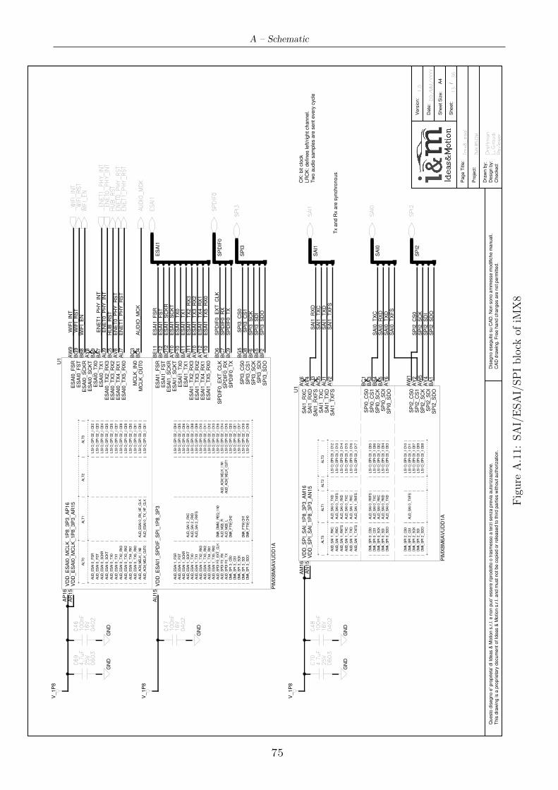
A – Schematic
Dra
wn b
y:
Checked:
Desig
n b
y:
Pro
ject:
Sheet S
ize:
Page T
itle
:
Date
:
Vers
ion:
CA
D d
raw
ing. F
ree h
and c
hanges a
re n
ot perm
itte
d.
Dis
egno e
seguito s
u C
AD
. N
on s
ono a
mm
esse m
odific
he m
anuali.
This
dra
win
g is a
pro
prieta
ry d
ocum
ent of Id
eas &
Motion s
.r.l. and m
ust not be c
opie
d o
r re
leased to third p
art
ies w
ithout auth
orization.
Questo
dis
egno e
' pro
prieta
' di Id
eas &
Motion s
.r.l. e n
on p
uo' e
ssere
rip
rodotto o
tra
sm
esso a
terz
i senza p
revia
auto
rizzazio
ne.
Sheet:
/A4
13
L.
Gir
au
di
iMX
8S
OM
Dra
ftm
an
imx
8_
es
ai
Re
vie
we
r
DD
/M
M/
YY
YY
1.0
36
SA
I1_R
XC
SA
I1_R
XD
SA
I1_R
XF
SS
AI1
_T
XC
SA
I1_T
XD
SA
I1_T
XF
S
SP
I0_C
S0
SP
I0_C
S1
SP
I0_S
CK
SP
I0_S
DI
SP
I0_S
DO
SP
I2_C
S0
SP
I2_C
S1
SP
I2_S
CK
SP
I2_S
DI
SP
I2_S
DO
VD
D_S
PI_
SA
I_1P
8_3P
3_A
M16
VD
D_S
PI_
SA
I_1P
8_3P
3_A
N15
+-
--
--
--
--
--
--
--
+-
--
--
--
--
--
--
--
+-
--
--
-+
--
--
--
--
--
--
--
--
-+
|
AL
T0
|
AL
T1
|
AL
T2
|
AL
T3
|
+-
--
--
--
--
--
--
--
+-
--
--
--
--
--
--
--
+-
--
--
-+
--
--
--
--
--
--
--
--
-+
|
AU
D_
SA
I1
_R
XC
|
AU
D_
SA
I0
_T
XD
|
|
L
SI
O_
GP
IO
3_
IO
12
|
|
AU
D_
SA
I1
_R
XD
|
AU
D_
SA
I0
_T
XF
S
|
|
L
SI
O_
GP
IO
3_
IO
13
|
|
AU
D_
SA
I1
_R
XF
S
|
AU
D_
SA
I0
_R
XD
|
|
L
SI
O_
GP
IO
3_
IO
14
|
|
AU
D_
SA
I1
_T
XC
|
AU
D_
SA
I0
_T
XC
|
|
L
SI
O_
GP
IO
3_
IO
15
|
|
AU
D_
SA
I1
_T
XD
|
AU
D_
SA
I1
_R
XC
|
|
L
SI
O_
GP
IO
3_
IO
16
|
|
AU
D_
SA
I1
_T
XF
S
|
AU
D_
SA
I1
_R
XF
S
|
|
L
SI
O_
GP
IO
3_
IO
17
|
|
DM
A_
SP
I0
_C
S0
|
AU
D_
SA
I0
_R
XF
S
|
|
L
SI
O_
GP
IO
3_
IO
05
|
|
DM
A_
SP
I0
_C
S1
|
AU
D_
SA
I0
_T
XC
|
|
L
SI
O_
GP
IO
3_
IO
06
|
|
DM
A_
SP
I0
_S
CK
|
AU
D_
SA
I0
_R
XC
|
|
L
SI
O_
GP
IO
3_
IO
02
|
|
DM
A_
SP
I0
_S
DI
|
AU
D_
SA
I0
_R
XD
|
|
L
SI
O_
GP
IO
3_
IO
04
|
|
DM
A_
SP
I0
_S
DO
|
AU
D_
SA
I0
_T
XD
|
|
L
SI
O_
GP
IO
3_
IO
03
|
|
DM
A_
SP
I2
_C
S0
|
|
|
L
SI
O_
GP
IO
3_
IO
10
|
|
DM
A_
SP
I2
_C
S1
|
AU
D_
SA
I0
_T
XF
S
|
|
L
SI
O_
GP
IO
3_
IO
11
|
|
DM
A_
SP
I2
_S
CK
|
|
|
L
SI
O_
GP
IO
3_
IO
07
|
|
DM
A_
SP
I2
_S
DI
|
|
|
L
SI
O_
GP
IO
3_
IO
09
|
|
DM
A_
SP
I2
_S
DO
|
|
|
L
SI
O_
GP
IO
3_
IO
08
|
+-
--
--
--
--
--
--
--
+-
--
--
--
--
--
--
--
+-
--
--
-+
--
--
--
--
--
--
--
--
-+
ES
AI0
_F
SR
ES
AI0
_F
ST
ES
AI0
_S
CK
RE
SA
I0_S
CK
TE
SA
I0_T
X0
ES
AI0
_T
X1
ES
AI0
_T
X2_R
X3
ES
AI0
_T
X3_R
X2
ES
AI0
_T
X4_R
X1
ES
AI0
_T
X5_R
X0
ES
AI1
_F
SR
ES
AI1
_F
ST
ES
AI1
_S
CK
RE
SA
I1_S
CK
TE
SA
I1_T
X0
ES
AI1
_T
X1
ES
AI1
_T
X2_R
X3
ES
AI1
_T
X3_R
X2
ES
AI1
_T
X4_R
X1
ES
AI1
_T
X5_R
X0
MC
LK
_IN
0M
CLK
_O
UT
0
SP
DIF
0_E
XT
_C
LK
SP
DIF
0_R
XS
PD
IF0_T
X
SP
I3_C
S0
SP
I3_C
S1
SP
I3_S
CK
SP
I3_S
DI
SP
I3_S
DO
VD
D_E
SA
I0_M
CLK
_1P
8_3P
3_A
P16
VD
D_E
SA
I0_M
CLK
_1P
8_3P
3_A
R15
VD
D_E
SA
I1_S
PD
IF_S
PI_
1P
8_3P
3
+-
--
--
--
--
--
--
--
--
--
-+
--
--
--
--
--
--
--
--
--
--
-+
--
--
--
--
--
--
--
--
--
-+
--
--
--
--
--
--
--
--
-+
|
A
LT
0
|
AL
T1
|
A
LT
2
|
AL
T3
|
+-
--
--
--
--
--
--
--
--
--
-+
--
--
--
--
--
--
--
--
--
--
-+
--
--
--
--
--
--
--
--
--
-+
--
--
--
--
--
--
--
--
-+
|
AU
D_
ES
AI
0_
FS
R
|
|
|
L
SI
O_
GP
IO
2_
IO
22
|
|
AU
D_
ES
AI
0_
FS
T
|
|
|
L
SI
O_
GP
IO
2_
IO
23
|
|
AU
D_
ES
AI
0_
SC
KR
|
|
|
L
SI
O_
GP
IO
2_
IO
24
|
|
AU
D_
ES
AI
0_
SC
KT
|
|
|
L
SI
O_
GP
IO
2_
IO
25
|
|
AU
D_
ES
AI
0_
TX
0
|
|
|
L
SI
O_
GP
IO
2_
IO
26
|
|
AU
D_
ES
AI
0_
TX
1
|
|
|
L
SI
O_
GP
IO
2_
IO
27
|
|
AU
D_
ES
AI
0_
TX
2_
RX
3
|
|
|
L
SI
O_
GP
IO
2_
IO
28
|
|
AU
D_
ES
AI
0_
TX
3_
RX
2
|
|
|
L
SI
O_
GP
IO
2_
IO
29
|
|
AU
D_
ES
AI
0_
TX
4_
RX
1
|
|
|
L
SI
O_
GP
IO
2_
IO
30
|
|
AU
D_
ES
AI
0_
TX
5_
RX
0
|
|
|
L
SI
O_
GP
IO
2_
IO
31
|
|
AU
D_
AC
M_
MC
LK
_I
N0
|
A
UD
_E
SA
I0
_R
X_
HF
_C
LK
|
|
L
SI
O_
GP
IO
3_
IO
00
|
|
AU
D_
AC
M_
MC
LK
_O
UT
0
|
A
UD
_E
SA
I0
_T
X_
HF
_C
LK
|
|
L
SI
O_
GP
IO
3_
IO
01
|
|
AU
D_
ES
AI
1_
FS
R
|
|
|
L
SI
O_
GP
IO
2_
IO
04
|
|
AU
D_
ES
AI
1_
FS
T
|
|
|
L
SI
O_
GP
IO
2_
IO
05
|
|
AU
D_
ES
AI
1_
SC
KR
|
|
|
L
SI
O_
GP
IO
2_
IO
06
|
|
AU
D_
ES
AI
1_
SC
KT
|
A
UD
_S
AI
2_
RX
C
|
|
L
SI
O_
GP
IO
2_
IO
07
|
|
AU
D_
ES
AI
1_
TX
0
|
A
UD
_S
AI
2_
RX
D
|
|
L
SI
O_
GP
IO
2_
IO
08
|
|
AU
D_
ES
AI
1_
TX
1
|
A
UD
_S
AI
2_
RX
FS
|
|
L
SI
O_
GP
IO
2_
IO
09
|
|
AU
D_
ES
AI
1_
TX
2_
RX
3
|
|
|
L
SI
O_
GP
IO
2_
IO
10
|
|
AU
D_
ES
AI
1_
TX
3_
RX
2
|
|
|
L
SI
O_
GP
IO
2_
IO
11
|
|
AU
D_
ES
AI
1_
TX
4_
RX
1
|
|
|
L
SI
O_
GP
IO
2_
IO
12
|
|
AU
D_
ES
AI
1_
TX
5_
RX
0
|
|
|
L
SI
O_
GP
IO
2_
IO
13
|
|
AU
D_
SP
DI
F0
_E
XT
_C
LK
|
D
MA
_D
MA
0_
RE
Q_
IN
0
|
|
L
SI
O_
GP
IO
2_
IO
16
|
|
AU
D_
SP
DI
F0
_R
X
|
A
UD
_M
QS
_R
|
A
UD
_A
CM
_M
CL
K_
IN
1
|
L
SI
O_
GP
IO
2_
IO
14
|
|
AU
D_
SP
DI
F0
_T
X
|
A
UD
_M
QS
_L
|
A
UD
_A
CM
_M
CL
K_
OU
T1
|
L
SI
O_
GP
IO
2_
IO
15
|
|
DM
A_
SP
I3
_C
S0
|
D
MA
_F
TM
_C
H2
|
|
L
SI
O_
GP
IO
2_
IO
20
|
|
DM
A_
SP
I3
_C
S1
|
|
|
L
SI
O_
GP
IO
2_
IO
21
|
|
DM
A_
SP
I3
_S
CK
|
|
|
L
SI
O_
GP
IO
2_
IO
17
|
|
DM
A_
SP
I3
_S
DI
|
D
MA
_F
TM
_C
H1
|
|
L
SI
O_
GP
IO
2_
IO
19
|
|
DM
A_
SP
I3
_S
DO
|
D
MA
_F
TM
_C
H0
|
|
L
SI
O_
GP
IO
2_
IO
18
|
+-
--
--
--
--
--
--
--
--
--
-+
--
--
--
--
--
--
--
--
--
--
-+
--
--
--
--
--
--
--
--
--
-+
--
--
--
--
--
--
--
--
-+
SA
I1
SA
I1
SA
I0
SA
I0
SA
I1_T
XF
S
SA
I1_T
XC
SA
I1_T
XD
SA
I1_R
XD
SA
I0_T
XF
SS
AI0
_T
XD
SA
I0_R
XD
SA
I0_T
XC
SP
I3
SP
I3
V_1P
8
V_1P
8
GN
DG
ND
ES
AI1
ES
AI1
_F
SR
ES
AI1
_F
ST
ES
AI1
_S
CK
RE
SA
I1_S
CK
TE
SA
I1_T
X0
ES
AI1
_T
X1
ES
AI1
_T
X2_R
X3
ES
AI1
_T
X3_R
X2
ES
AI1
_T
X4_R
X1
ES
AI1
_T
X5_R
X0
SP
DIF
0_E
XT
_C
LK
SP
DIF
0_R
XS
PD
IF0_T
X
HU
B_R
ST
EN
ET
0_P
HY
_R
ST
EN
ET
1_P
HY
_R
ST
_E
NE
T0
_P
HY
_IN
T_
EN
ET1
_P
HY
_IN
T_E
NE
T0_P
HY
_IN
T_E
NE
T1_P
HY
_IN
T
AU
DIO
_M
CK
AU
DIO
_M
CK
AW
9B
G9
BB
8A
Y8
BA
9B
A7
AU
9B
C5
AV
8A
U7
BE
11
BF
12
BD
12
AY
10
BF
10
BA
11
AU
11
AV
10
AY
12
AT
10
BC
3B
D4
BD
6B
C7
BC
9
BG
5B
D8
BF
6B
E5
BF
2
AP
16
AR
15
AU
15
PIM
X8M
6A
VU
DD
1A
U1
C4
6
04
02
10
0n
F1
6V
C4
7
04
02
10
0n
F1
6V
GN
D
SP
I2WIF
I_E
N_
WIF
I_R
ST
SP
I2
WIF
I_E
N_W
IFI_
RS
T_W
IFI_
INT
SP
I2_C
S0
SP
I2_S
CK
SP
I2_S
DI
SP
I2_S
DO
25
V4
.7u
F
06
03
C6
9
GN
DG
ND
V_1P
8
C4
8
04
02
10
0n
F1
6V
C7
0
25
V4
.7u
F
06
03
SP
DIF
0
SP
I3_S
CK
_S
PI3
_C
S0
_S
PI3
_C
S1
SP
I3_S
DI
SP
I3_S
DO
AV
6A
V4
AU
3A
U5
AU
1A
V2
BC
1B
A3
BB
4B
A5
AY
6
AW
1A
Y2
AW
5A
Y4
BA
1
AM
16
AN
15
PIM
X8M
6A
VU
DD
1A
U1
HU
B_
RS
T
ES
AI1
SP
DIF
0
_W
IFI_
INT
EN
ET1
_P
HY
_R
ST
EN
ET0
_P
HY
_R
ST
Tx a
nd R
x a
re s
ynchro
nous
CK
: bit c
lock
LR
CK
: defines left/r
ight channel.
Tw
o a
udio
sam
ple
s a
re s
ent every
cycle
Figure
A.11:
SAI/ESAI/SPIblock
ofiM
X8
75
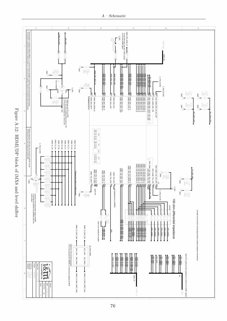
A – Schematic
Dra
wn b
y:
Checked:
Desig
n b
y:
Pro
ject:
Sheet S
ize:
Page T
itle:
Sheet:
Date
:
Vers
ion:
CA
D d
raw
ing. F
ree h
and c
hanges a
re n
ot p
erm
itted.
Dis
egno e
seguito
su C
AD
. Non s
ono a
mm
esse m
odific
he m
anuali.
This
dra
win
g is
a p
roprie
tary
docum
ent o
f Ideas &
Motio
n s
.r.l. and m
ust n
ot b
e c
opie
d o
r rele
ased to
third
partie
s w
ithout a
uth
oriz
atio
n.
Questo
dis
egno e
' pro
prie
ta' d
i Ideas &
Motio
n s
.r.l. e n
on p
uo' e
ssere
ripro
dotto
o tra
sm
esso a
terz
i senza p
revia
auto
rizzazio
ne.
/ A3
12
34
56
78
ABCDEF
HD
MI_
RX
0_A
RC
_N
HD
MI_
RX
0_A
RC
_P
HD
MI_
RX
0_C
EC
HD
MI_
RX
0_C
LK
_N
HD
MI_
RX
0_C
LK
_P
HD
MI_
RX
0_D
AT
A0_N
HD
MI_
RX
0_D
AT
A0_P
HD
MI_
RX
0_D
AT
A1_N
HD
MI_
RX
0_D
AT
A1_P
HD
MI_
RX
0_D
AT
A2_N
HD
MI_
RX
0_D
AT
A2_P
HD
MI_
RX
0_D
DC
_S
CL
HD
MI_
RX
0_D
DC
_S
DA
HD
MI_
RX
0_H
PD
HD
MI_
RX
0_M
ON
_5V
HD
MI_
RX
0_R
EX
T
HD
MI_
TX
0_A
UX
_N
HD
MI_
TX
0_A
UX
_P
HD
MI_
TX
0_C
EC
HD
MI_
TX
0_C
LK
_E
DP
3_N
HD
MI_
TX
0_C
LK
_E
DP
3_P
HD
MI_
TX
0_D
AT
A0_E
DP
2_N
HD
MI_
TX
0_D
AT
A0_E
DP
2_P
HD
MI_
TX
0_D
AT
A1_E
DP
1_N
HD
MI_
TX
0_D
AT
A1_E
DP
1_P
HD
MI_
TX
0_D
AT
A2_E
DP
0_N
HD
MI_
TX
0_D
AT
A2_E
DP
0_P
HD
MI_
TX
0_D
DC
_S
CL
HD
MI_
TX
0_D
DC
_S
DA
HD
MI_
TX
0_H
PD
HD
MI_
TX
0_T
S_S
CL
HD
MI_
TX
0_T
S_S
DA
HD
MI_
TX
0_R
EX
T
VD
D_H
DM
I_R
X0_1P
8
VD
D_H
DM
I_R
X0_LD
O0_1P
0_C
AP
VD
D_H
DM
I_R
X0_LD
O1_1P
0_C
AP
VD
D_H
DM
I_R
X0_V
H_R
X_3P
3
VD
D_H
DM
I_T
X0_1P
0
VD
D_H
DM
I_T
X0_1P
8
VD
D_H
DM
I_T
X0_D
IG_3P
3
VD
D_H
DM
I_T
X0_LD
O_1P
0_C
AP
+-
--
--
--
--
--
--
--
--
--
+-
--
--
--
--
--
--
-+
--
--
--
+-
--
--
--
--
--
--
--
--
+
|
AL
T0
|
AL
T1
|
A
LT
2
|
A
LT
3
|
+-
--
--
--
--
--
--
--
--
--
+-
--
--
--
--
--
--
-+
--
--
--
+-
--
--
--
--
--
--
--
--
+
|
HD
MI
_T
X0
_I
2C
0_
SC
L
|
DM
A_
I2
C0
_S
CL
|
|
LS
IO
_G
PI
O2
_I
O0
2
|
|
HD
MI
_T
X0
_I
2C
0_
SD
A
|
DM
A_
I2
C0
_S
DA
|
|
LS
IO
_G
PI
O2
_I
O0
3
|
+-
--
--
--
--
--
--
--
--
--
+-
--
--
--
--
--
--
-+
--
--
--
+-
--
--
--
--
--
--
--
--
+
DP
HD
MI_
TX
HD
MI_
TX
_C
K-
HD
MI_
TX
_C
K+
HD
MI_
TX
_D
DC
_S
CL
HD
MI_
TX
_D
DC
_S
DA
HD
MI_
TX
_D
0-
HD
MI_
TX
_D
0+
HD
MI_
TX
_D
1-
HD
MI_
TX
_D
1+
HD
MI_
TX
_D
2-
HD
MI_
TX
_D
2+
HD
MI_
TX
_H
PD
DP
0_LA
NE
3-
DP
0_LA
NE
3+
DP
0_A
UX
+D
P0_A
UX
-
DP
0_LA
NE
2-
DP
0_LA
NE
2+
DP
0_LA
NE
1-
DP
0_LA
NE
1+
DP
0_LA
NE
0-
DP
0_LA
NE
0+
DP
0_H
PD
HD
MI_
TX
_D
0-
HD
MI_
TX
_D
0+
HD
MI_
TX
_D
1-
HD
MI_
TX
_D
1+
HD
MI_
TX
_D
2-
HD
MI_
TX
_D
2+
DP
0_LA
NE
3-
DP
0_LA
NE
3+
DP
0_LA
NE
2-
DP
0_LA
NE
2+
DP
0_LA
NE
1-
DP
0_LA
NE
1+
DP
0_LA
NE
0-
DP
0_LA
NE
0+
HD
MI_
TX
_H
PD
DP
0_H
PD
HD
MI_
TX
_C
K-
HD
MI_
TX
_C
K+
HD
MI_
TX
_D
DC
_S
HIF
T_S
CL
HD
MI_
TX
_D
DC
_S
HIF
T_S
DA
spare
I2C
GN
D
HD
MI_
TX
_D
0-
HD
MI_
TX
_D
0+
HD
MI_
TX
_D
1-
HD
MI_
TX
_D
1+
HD
MI_
TX
_D
2-
HD
MI_
TX
_D
2+
HD
MI_
TX
_C
K-
HD
MI_
TX
_C
K+
GN
D
Passiv
e le
vel s
hifte
r for H
DM
I sig
nals
DP
0_A
UX
+D
P0_A
UX
-
AU
X is
On-m
odule
AC
couple
d
pla
ce A
C-c
ouplin
g s
erie
s c
apacito
rs o
n c
arrie
r for 8
LA
NE
x s
ignals
TX
_LD
O_C
AP
TX
_LD
O_C
AP
GN
DG
ND
HD
MI_
RX
GN
D
HD
MI_
RX
0_M
ON
_5V
HD
MI_
RX
0_A
RC
+H
DM
I_R
X0_A
RC
-
HD
MI_
RX
0_H
PD
HD
MI_
RX
0_C
EC
HD
MI_
RX
0_D
DC
_S
DA
HD
MI_
RX
0_D
DC
_S
CL
HD
MI_
RX
0_C
LK
+H
DM
I_R
X0_C
LK
-
HD
MI_
RX
0_D
AT
A0+
HD
MI_
RX
0_D
AT
A1-
HD
MI_
RX
0_D
AT
A1+
HD
MI_
RX
0_D
AT
A2-
HD
MI_
RX
0_D
AT
A2+
HD
MI_
RX
0_D
AT
A0-
RX
_LD
O0_C
AP
RX
_LD
O0_C
AP
GN
DG
ND
RX
_LD
O1_C
AP
RX
_LD
O1_C
AP
GN
DG
ND
No d
edic
ate
d p
in o
n S
MA
RC
100 o
hm
diffe
rentia
l impedance
Consid
er h
ow
the 0
ohm
can b
e p
laced w
ithout c
reatin
g im
pedance m
ism
atc
hes
varia
nts
GN
D
AY VC
C
GN
D
GN
D
HP
D
HP
D
GN
D
HD
MI_
RX
0_M
ON
_5V
On th
e S
ink s
ide, o
nly
SC
L n
eed a
pullu
pof 4
7k (fro
m H
DM
I Spec)
Re
vie
we
r
Dra
ftma
n
iMX
8S
OM
L. G
irau
di
14
36
1.0
DD
/M
M/
YY
YY
imx
8_
DP
_H
DM
I
DP
HD
MI_
TX
V_3P
3
V_1P
8_F
ILT
ER
V_3P
3V_1P
8_F
ILT
ER
HD
MI_
RX
V_1P
8_F
ILT
ER V
_3P
3_F
ILT
ER
V_3P
3
HD
MI s
ays th
at V
ih fo
r HP
D
is 3
V: th
e s
marc
inste
ad w
ants
a p
in a
t 1.8
Vso th
is p
ort tra
nsla
tes fro
m 1
.8V
to 3
.3V
Connect to
the s
am
e p
ow
er s
upply
of H
DM
I: in
this
way th
e p
ulld
ow
n a
re d
isable
d w
hen th
eim
x8 is
dow
n
HD
MI_
TX
_D
DC
_S
CL
HD
MI_
TX
_D
DC
_S
DA
SC
L_LO
W
SD
A_LO
W
SC
L_H
IGH
SD
A_H
IGH
i2c_le
vel_
shifte
r
HD
MI_
TX
_D
DC
_S
HIF
T_S
CL
HD
MI_
TX
_D
DC
_S
HIF
T_S
DA
Shift fro
m 1
.8 to
3.3
and v
icevers
a1.8
V is
the w
ante
d fro
m S
MA
RC
, 3.3
should
be re
adable
by iM
X8
GN
D
BM
4
BL3
BK
2
BJ1
BH
2B
G3
BJ11
BN
11
BF
14
BE
13
BH
10
BM
20
BL19
BM
18
BL17
BM
16
BL15
BM
12
BL11
BJ9
BM
14
BL13
U1
PIM
X8M
6A
VU
DD
1A
AW
15
AW
21
AW
17
AV
16
AV
20
AU
21
AU
19
AV
18
BJ7
BN
7B
N9
BH
8
BN
5B
G1
BL9
BM
8
BL7
BM
6
BL5
M3
PM
DT2
90
UN
E3
80
m2
0V
5
34
C4
11
00
nF
C4
21
00
nF
C4
31
00
nF
C3
60
40
21
00
nF
16
V
C4
01
00
nF
C3
71
00
nF
C3
81
00
nF
C3
91
00
nF
R5
3
04
02
10
0K
1%
U6
74LV
1T
34G
W
3
5
42R9
30
40
201
%
C4
4
04
02
10
0n
F1
6V
16
V1
00
nF
04
02
C4
5
R7
30
40
24
7K
1%
DS
6N
SR
05
T4
0P
2T5
G
2
1
R1
37
04
02
27
K1
%
R9
9
06
03
49
9
1%
R8
30
40
20 1
%
0R
84
R8
500
R8
6
R8
700
R8
8
C2
34
04
02
22
0n
F1
6V
0R
89
R9
00
10
V2
.2u
F
04
02
C3
16
10
V1
uF
04
02
C1
31
04
02
1%
0R
91
04
02
1%
0R
92
10
V1
uF
04
02
C1
32
10
V2
.2u
F
04
02
C3
17
R9
8
06
03
49
9
1%
R1
29
04
02
60
4
1%
1%
60
40
40
2
R1
30
1%
60
40
40
2
R1
31
1%
60
40
40
2
R1
32
R1
33
04
02
60
4
1%
1%
60
40
40
2
R1
34
R1
35
04
02
60
4
1%
1%
60
40
40
2
R1
36
16
V1
00
nF
04
02
C3
4
C3
51
00
nF
C1
30
04
02
1u
F1
0V
C3
15
04
02
2.2
uF
10
V
Figu
reA.12:
HDMI/D
Pblock
ofiM
X8an
dlevel
shifter
76
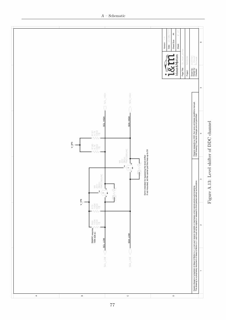
A – Schematic
V_1P
8
V_3P
3
SD
A_
LO
WS
DA
_H
IGH
SC
L_LO
W
SD
A_LO
WS
DA
_H
IGH
SM
AR
C r
equires
100k w
ak p
u
CA
D d
raw
ing. F
ree h
and c
hanges a
re n
ot perm
itte
d.
Dis
egno e
seguito s
u C
AD
. N
on s
ono a
mm
esse m
odific
he m
anuali.
This
dra
win
g is a
pro
prieta
ry d
ocum
ent of Id
eas &
Motion s
.r.l. and m
ust not be c
opie
d o
r re
leased to third p
art
ies w
ithout auth
orization.
Questo
dis
egno e
' pro
prieta
' di Id
eas &
Motion s
.r.l. e n
on p
uo' e
ssere
rip
rodotto o
tra
sm
esso a
terz
i senza p
revia
auto
rizzazio
ne.
Dra
wn b
y:
Checked:
Desig
n b
y:
Pro
ject:
Sheet S
ize:
Page T
itle
:
Sheet:
Date
:
Vers
ion:
/A4
A B C D
12
34
56
Re
vie
we
rL
. G
ira
ud
i
iMX
8S
OM
Dra
ftm
an
37
1.0
DD
/M
M/
YY
YY
i2c
_le
ve
l_s
hif
ter
SC
L_
LO
WS
CL_
HIG
HS
CL_H
IGH
0ohm
inte
nded for
bypassin
g the level shifte
rIf n
ot m
ounte
d, le
t th
e c
arr
ier
pull
the lin
es u
p to 5
V
20
V3
80
mP
MD
T2
90
UN
E
M4
53
42
0V
38
0m
PM
DT2
90
UN
E
M4
26
1
04
02
R6
9
1%
10
0K
04
02
R7
0
1%
10
0K
R1
60
04
02
4.7
K
1%
1%
4.7
K0
40
2
R1
61
R9
40
40
20 1
%
1%
00
40
2R
95
Figure
A.13:
Level
shifterof
DDC
chan
nel
77
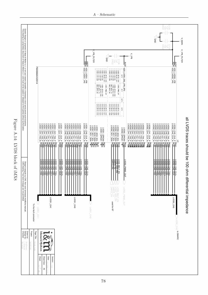
A – Schematic
Dra
wn b
y:
Checked:
Desig
n b
y:
Pro
ject:
Sheet S
ize:
Page T
itle:
Date
:
Vers
ion:
CA
D d
raw
ing. F
ree h
and c
hanges a
re n
ot p
erm
itted.
Dis
egno e
seguito
su C
AD
. Non s
ono a
mm
esse m
odific
he m
anuali.
This
dra
win
g is
a p
roprie
tary
docum
ent o
f Ideas &
Motio
n s
.r.l. and m
ust n
ot b
e c
opie
d o
r rele
ased to
third
partie
s w
ithout a
uth
oriz
atio
n.
Questo
dis
egno e
' pro
prie
ta' d
i Ideas &
Motio
n s
.r.l. e n
on p
uo' e
ssere
ripro
dotto
o tra
sm
esso a
terz
i senza p
revia
auto
rizzazio
ne.
Sheet:
/ A4
15
L. G
irau
di
iMX
8S
OM
Dra
ftma
n
imx
8_
lvd
s
Re
vie
we
r
DD
/M
M/
YY
YY
1.0
36
LV
DS
0_C
H0_C
LK
_N
LV
DS
0_C
H0_C
LK
_P
LV
DS
0_C
H0_T
X0_N
LV
DS
0_C
H0_T
X0_P
LV
DS
0_C
H0_T
X1_N
LV
DS
0_C
H0_T
X1_P
LV
DS
0_C
H0_T
X2_N
LV
DS
0_C
H0_T
X2_P
LV
DS
0_C
H0_T
X3_N
LV
DS
0_C
H0_T
X3_P
LV
DS
0_C
H1_C
LK
_N
LV
DS
0_C
H1_C
LK
_P
LV
DS
0_C
H1_T
X0_N
LV
DS
0_C
H1_T
X0_P
LV
DS
0_C
H1_T
X1_N
LV
DS
0_C
H1_T
X1_P
LV
DS
0_C
H1_T
X2_N
LV
DS
0_C
H1_T
X2_P
LV
DS
0_C
H1_T
X3_N
LV
DS
0_C
H1_T
X3_P
LV
DS
0_G
PIO
00
LV
DS
0_G
PIO
01
LV
DS
0_I2
C0_S
CL
LV
DS
0_I2
C0_S
DA
LV
DS
0_I2
C1_S
CL
LV
DS
0_I2
C1_S
DA
LV
DS
1_C
H0_C
LK
_N
LV
DS
1_C
H0_C
LK
_P
LV
DS
1_C
H0_T
X0_N
LV
DS
1_C
H0_T
X0_P
LV
DS
1_C
H0_T
X1_N
LV
DS
1_C
H0_T
X1_P
LV
DS
1_C
H0_T
X2_N
LV
DS
1_C
H0_T
X2_P
LV
DS
1_C
H0_T
X3_N
LV
DS
1_C
H0_T
X3_P
LV
DS
1_C
H1_C
LK
_N
LV
DS
1_C
H1_C
LK
_P
LV
DS
1_C
H1_T
X0_N
LV
DS
1_C
H1_T
X0_P
LV
DS
1_C
H1_T
X1_N
LV
DS
1_C
H1_T
X1_P
LV
DS
1_C
H1_T
X2_N
LV
DS
1_C
H1_T
X2_P
LV
DS
1_C
H1_T
X3_N
LV
DS
1_C
H1_T
X3_P
LV
DS
1_G
PIO
00
LV
DS
1_G
PIO
01
LV
DS
1_I2
C0_S
CL
LV
DS
1_I2
C0_S
DA
LV
DS
1_I2
C1_S
CL
LV
DS
1_I2
C1_S
DA
VD
D_LV
DS
0_1P
0V
DD
_LV
DS
0_1P
8
VD
D_LV
DS
1_1P
0V
DD
_LV
DS
1_1P
8
VD
D_LV
DS
_D
IG_1P
8_3P
3+
--
--
--
--
--
--
--
--
--
+-
--
--
--
--
--
--
--
--
-+
--
--
--
+-
--
--
--
--
--
--
--
--
+
|
AL
T0
|
A
LT
1
|
AL
T2
|
AL
T3
|
+-
--
--
--
--
--
--
--
--
-+
--
--
--
--
--
--
--
--
--
+-
--
--
-+
--
--
--
--
--
--
--
--
-+
|
LV
DS
0_
GP
IO
0_
IO
00
|
L
VD
S0
_P
WM
0_
OU
T
|
|
L
SI
O_
GP
IO
1_
IO
04
|
|
LV
DS
0_
GP
IO
0_
IO
01
|
|
|
L
SI
O_
GP
IO
1_
IO
05
|
|
LV
DS
0_
I2
C0
_S
CL
|
L
VD
S0
_G
PI
O0
_I
O0
2
|
|
L
SI
O_
GP
IO
1_
IO
06
|
|
LV
DS
0_
I2
C0
_S
DA
|
L
VD
S0
_G
PI
O0
_I
O0
3
|
|
L
SI
O_
GP
IO
1_
IO
07
|
|
LV
DS
0_
I2
C1
_S
CL
|
D
MA
_U
AR
T2
_T
X
|
|
L
SI
O_
GP
IO
1_
IO
08
|
|
LV
DS
0_
I2
C1
_S
DA
|
D
MA
_U
AR
T2
_R
X
|
|
L
SI
O_
GP
IO
1_
IO
09
|
|
LV
DS
1_
GP
IO
0_
IO
00
|
L
VD
S1
_P
WM
0_
OU
T
|
|
L
SI
O_
GP
IO
1_
IO
10
|
|
LV
DS
1_
GP
IO
0_
IO
01
|
|
|
L
SI
O_
GP
IO
1_
IO
11
|
|
LV
DS
1_
I2
C0
_S
CL
|
L
VD
S1
_G
PI
O0
_I
O0
2
|
|
L
SI
O_
GP
IO
1_
IO
12
|
|
LV
DS
1_
I2
C0
_S
DA
|
L
VD
S1
_G
PI
O0
_I
O0
3
|
|
L
SI
O_
GP
IO
1_
IO
13
|
|
LV
DS
1_
I2
C1
_S
CL
|
D
MA
_U
AR
T3
_T
X
|
|
L
SI
O_
GP
IO
1_
IO
14
|
|
LV
DS
1_
I2
C1
_S
DA
|
D
MA
_U
AR
T3
_R
X
|
|
L
SI
O_
GP
IO
1_
IO
15
|
+-
--
--
--
--
--
--
--
--
-+
--
--
--
--
--
--
--
--
--
+-
--
--
-+
--
--
--
--
--
--
--
--
-+
U1
AV
32
AW
33
AW
35
AV
34
AV
36
BN
35
BD
32
BE
33
BL35
BH
36
BD
34
BM
30
BK
30
BN
31
BL31
BM
32
BK
32
BN
33
BL33
BM
34
BK
34
BM
40
BK
40
BN
39
BL39
BM
38
BK
38
BN
37
BL37
BM
36
BK
36
BE
35
BE
37
BD
36
BD
38
BD
40
BE
39
BH
38
BG
37
BH
40
BG
39
BH
42
BG
41
BH
44
BG
43
BH
46
BG
45
BN
45
BL45
BM
44
BK
44
BN
43
BL43
BM
42
BK
42
BN
41
BL41
PIM
X8M
6A
VU
DD
1A
V_1P
8_F
ILT
ER
V_1P
8_F
ILT
ER
V_M
AIN
V_1P
8
LV
DS
1_C
H1
LV
DS
1_C
H0_C
LK
+LV
DS
1_C
H0_C
LK
-
LV
DS
1_C
H0_T
X0-
LV
DS
1_C
H0_T
X0+
LV
DS
1_C
H0_T
X1+
LV
DS
1_C
H0_T
X1-
LV
DS
1_C
H0_T
X2-
LV
DS
1_C
H0_T
X2+
LV
DS
1_C
H0_T
X3-
LV
DS
1_C
H0_T
X3+
LV
DS
1_C
H1_C
LK
-LV
DS
1_C
H1_C
LK
+
LV
DS
1_C
H1_T
X0-
LV
DS
1_C
H1_T
X0+
LV
DS
1_C
H1_T
X1-
LV
DS
1_C
H1_T
X1+
LV
DS
1_C
H1_T
X2-
LV
DS
1_C
H1_T
X2+
LV
DS
1_C
H1_T
X3-
LV
DS
1_C
H1_T
X3+
all L
VD
S tra
ces s
hould
be 1
00 o
hm
diffe
rentia
l impedance
LV
DS
0_
CH
0
LV
DS
0_C
H0
LV
DS
0_C
H0_C
LK
-LV
DS
0_C
H0_C
LK
+
LV
DS
0_C
H0_T
X0-
LV
DS
0_C
H0_T
X0+
LV
DS
0_C
H0_T
X1-
LV
DS
0_C
H0_T
X1+
LV
DS
0_C
H0_T
X2-
LV
DS
0_C
H0_T
X2+
LV
DS
0_C
H0_T
X3-
LV
DS
0_C
H0_T
X3+
LV
DS
0_P
WM
0_O
UT
LC
D0_B
KLT
_E
NLC
D0_V
DD
_E
NLC
D0
_V
DD
_E
N
LV
DS
0_
PW
M0
_O
UTTo th
e A
uX
connecto
r
to S
MA
RC
UA
RT2
_R
XU
AR
T2
_TX
UA
RT
2_R
XU
AR
T2_T
Xused fo
r BT
C1
34
04
02
1u
F1
0V
GN
D
10
V1
uF
04
02
C1
35
LV
DS
1_C
H0 LV
DS
1_
CH
0
LV
DS
1_
CH
1
10
V1
uF
04
02
C1
36
GN
D
LC
D0
_B
KLT_
EN
Figu
reA.14:
LVDSblock
ofiM
X8
78
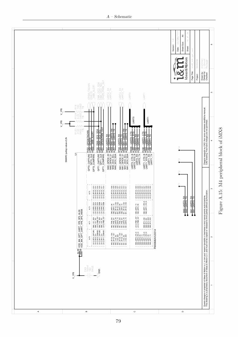
A – Schematic
GP
T0_C
AP
TU
RE
GP
T0_C
LK
GP
T0_C
OM
PA
RE
GP
T1_C
AP
TU
RE
GP
T1_C
LK
GP
T1_C
OM
PA
RE
M40_G
PIO
0_00
M40_G
PIO
0_01
M40_I2
C0_S
CL
M40_I2
C0_S
DA
M41_G
PIO
0_00
M41_G
PIO
0_01
M41_I2
C0_S
CL
M41_I2
C0_S
DA
UA
RT
0_C
TS
_B
UA
RT
0_R
TS
_B
UA
RT
0_R
XU
AR
T0_T
X
UA
RT
1_C
TS
_B
UA
RT
1_R
TS
_B
UA
RT
1_R
XU
AR
T1_T
X
VD
D_M
4_G
PT
_U
AR
T_1P
8_3P
3_A
L39
VD
D_M
4_G
PT
_U
AR
T_1P
8_3P
3_A
M38
+-
--
--
--
--
--
--
--
--
--
+-
--
--
--
--
--
--
--
+-
--
--
--
--
--
--
--
--
+-
--
--
--
--
--
--
--
--
+
|
AL
T0
|
AL
T1
|
A
LT
2
|
A
LT
3
|
+-
--
--
--
--
--
--
--
--
--
+-
--
--
--
--
--
--
--
+-
--
--
--
--
--
--
--
--
+-
--
--
--
--
--
--
--
--
+
|
LS
IO
_G
PT
0_
CA
PT
UR
E
|
DM
A_
I2
C1
_S
DA
|
LS
IO
_K
PP
0_
CO
L5
|
LS
IO
_G
PI
O0
_I
O1
5
|
|
LS
IO
_G
PT
0_
CL
K
|
DM
A_
I2
C1
_S
CL
|
LS
IO
_K
PP
0_
CO
L4
|
LS
IO
_G
PI
O0
_I
O1
4
|
|
LS
IO
_G
PT
0_
CO
MP
AR
E
|
LS
IO
_P
WM
3_
OU
T
|
LS
IO
_K
PP
0_
CO
L6
|
LS
IO
_G
PI
O0
_I
O1
6
|
|
LS
IO
_G
PT
1_
CA
PT
UR
E
|
DM
A_
I2
C2
_S
DA
|
LS
IO
_K
PP
0_
RO
W4
|
LS
IO
_G
PI
O0
_I
O1
8
|
|
LS
IO
_G
PT
1_
CL
K
|
DM
A_
I2
C2
_S
CL
|
LS
IO
_K
PP
0_
CO
L7
|
LS
IO
_G
PI
O0
_I
O1
7
|
|
LS
IO
_G
PT
1_
CO
MP
AR
E
|
LS
IO
_P
WM
2_
OU
T
|
LS
IO
_K
PP
0_
RO
W5
|
LS
IO
_G
PI
O0
_I
O1
9
|
|
M4
0_
GP
IO
0_
IO
00
|
M4
0_
TP
M0
_C
H0
|
DM
A_
UA
RT
4_
RX
|
LS
IO
_G
PI
O0
_I
O0
8
|
|
M4
0_
GP
IO
0_
IO
01
|
M4
0_
TP
M0
_C
H1
|
DM
A_
UA
RT
4_
TX
|
LS
IO
_G
PI
O0
_I
O0
9
|
|
M4
0_
I2
C0
_S
CL
|
M4
0_
UA
RT
0_
RX
|
M4
0_
GP
IO
0_
IO
02
|
LS
IO
_G
PI
O0
_I
O0
6
|
|
M4
0_
I2
C0
_S
DA
|
M4
0_
UA
RT
0_
TX
|
M4
0_
GP
IO
0_
IO
03
|
LS
IO
_G
PI
O0
_I
O0
7
|
|
M4
1_
GP
IO
0_
IO
00
|
M4
1_
TP
M0
_C
H0
|
DM
A_
UA
RT
3_
RX
|
LS
IO
_G
PI
O0
_I
O1
2
|
|
M4
1_
GP
IO
0_
IO
01
|
M4
1_
TP
M0
_C
H1
|
DM
A_
UA
RT
3_
TX
|
LS
IO
_G
PI
O0
_I
O1
3
|
|
M4
1_
I2
C0
_S
CL
|
M4
1_
UA
RT
0_
RX
|
M4
1_
GP
IO
0_
IO
02
|
LS
IO
_G
PI
O0
_I
O1
0
|
|
M4
1_
I2
C0
_S
DA
|
M4
1_
UA
RT
0_
TX
|
M4
1_
GP
IO
0_
IO
03
|
LS
IO
_G
PI
O0
_I
O1
1
|
|
DM
A_
UA
RT
0_
CT
S_
B
|
LS
IO
_P
WM
1_
OU
T
|
DM
A_
UA
RT
2_
TX
|
LS
IO
_G
PI
O0
_I
O2
3
|
|
DM
A_
UA
RT
0_
RT
S_
B
|
LS
IO
_P
WM
0_
OU
T
|
DM
A_
UA
RT
2_
RX
|
LS
IO
_G
PI
O0
_I
O2
2
|
|
DM
A_
UA
RT
0_
RX
|
|
|
LS
IO
_G
PI
O0
_I
O2
0
|
|
DM
A_
UA
RT
0_
TX
|
|
|
LS
IO
_G
PI
O0
_I
O2
1
|
|
DM
A_
UA
RT
1_
CT
S_
B
|
DM
A_
SP
I3
_C
S0
|
DM
A_
UA
RT
1_
RT
S_
B
|
LS
IO
_G
PI
O0
_I
O2
7
|
|
DM
A_
UA
RT
1_
RT
S_
B
|
DM
A_
SP
I3
_S
DI
|
DM
A_
UA
RT
1_
CT
S_
B
|
LS
IO
_G
PI
O0
_I
O2
6
|
|
DM
A_
UA
RT
1_
RX
|
DM
A_
SP
I3
_S
DO
|
|
LS
IO
_G
PI
O0
_I
O2
5
|
|
DM
A_
UA
RT
1_
TX
|
DM
A_
SP
I3
_S
CK
|
|
LS
IO
_G
PI
O0
_I
O2
4
|
+-
--
--
--
--
--
--
--
--
--
+-
--
--
--
--
--
--
--
+-
--
--
--
--
--
--
--
--
+-
--
--
--
--
--
--
--
--
+
U1
AM
38
AL39
AY
48
AT
44
AR
43
AV
46
AV
48
AV
50
AU
45
AW
49
AU
49
AR
45
AU
47
AP
44
AU
51
AM
44
AU
53
AR
47
BA
51
BA
53
AY
50
AW
53
AY
52
AV
52
PIM
X8M
6A
VU
DD
1A
CA
D d
raw
ing. F
ree h
and c
hanges a
re n
ot perm
itte
d.
Dis
egno e
seguito s
u C
AD
. N
on s
ono a
mm
esse m
odific
he m
anuali.
This
dra
win
g is a
pro
prieta
ry d
ocum
ent of Id
eas &
Motion s
.r.l. and m
ust not be c
opie
d o
r re
leased to third p
art
ies w
ithout auth
orization.
Questo
dis
egno e
' pro
prieta
' di Id
eas &
Motion s
.r.l. e n
on p
uo' e
ssere
rip
rodotto o
tra
sm
esso a
terz
i senza p
revia
auto
rizzazio
ne.
Dra
wn b
y:
Checked:
Desig
n b
y:
Pro
ject:
Sheet S
ize:
Page T
itle
:
Sheet:
Date
:
Vers
ion:
/A4
A B C D
12
34
56
Re
vie
we
r
Dra
ftm
an
iMX
8S
OM
L.
Gir
au
di
16
36
1.0
DD
/M
M/
YY
YY
imx
8_
m4
_g
pt_
ua
rt
UA
RT1
UA
RT0
UA
RT
1
UA
RT
0
UA
RT
0_T
XU
AR
T0_R
X_U
AR
T0_R
TS
_U
AR
T0_C
TS
UA
RT
1_T
XU
AR
T1_R
X_U
AR
T1_R
TS
_U
AR
T1_C
TS
UA
RT3
_R
XU
AR
T3
_TX
UA
RT4
_TX
UA
RT4
_R
X
UA
RT
3_R
XU
AR
T3_T
X
UA
RT
4_T
XU
AR
T4_R
X
V_1P
8
DM
A_
I2C
2_
SD
AD
MA
_I2
C2
_S
CL
DM
A_I2
C2_S
DA
DM
A_I2
C2_S
CL
R1
23
04
02
2.2
K
1%
R1
24
04
02
2.2
K
1%
V_1P
8
GP
IO5
/P
WM
_O
UT
GP
IO5/P
WM
_O
UT
_S
MB
_A
LE
RT
_S
MB
_A
LE
RT
C4
9
04
02
10
0n
F1
6V
GN
D
M40_U
AR
T0_R
XM
40_U
AR
T0_T
X
M41_U
AR
T0_R
XM
41_U
AR
T0_T
X
M40_U
AR
T0_R
XM
40_U
AR
T0_T
X
M41_U
AR
T0_R
XM
41_U
AR
T0_T
X
T1
T2
T3
T4
1%
R1
91
0K
04
02
V_1P
8
GP
IO6
/TA
CH
ING
PIO
6/T
AC
HIN
GP
IO1
0G
PIO
10
SM
AR
C p
ullu
p v
alu
e=
2,2
k
Figure
A.15:
M4peripheral
block
ofiM
X8
79

A – Schematic
MLB
_C
LK
MLB
_C
LK
_N
MLB
_C
LK
_P
MLB
_D
AT
A
MLB
_D
AT
A_N
MLB
_D
AT
A_P
MLB
_S
IG
MLB
_S
IG_N
MLB
_S
IG_P
VD
D_M
LB
_1P
8
VD
D_M
LB
_D
IG_1P
8_3P
3
+-
--
--
--
--
--
--
--
+-
--
--
--
--
--
--
--
+-
--
--
-+
--
--
--
--
--
--
--
--
-+
|
AL
T0
|
AL
T1
|
AL
T2
|
AL
T3
|
+-
--
--
--
--
--
--
--
+-
--
--
--
--
--
--
--
+-
--
--
-+
--
--
--
--
--
--
--
--
-+
|
CO
NN
_M
LB
_C
LK
|
AU
D_
SA
I3
_R
XF
S
|
|
L
SI
O_
GP
IO
3_
IO
27
|
|
CO
NN
_M
LB
_D
AT
A
|
AU
D_
SA
I3
_R
XD
|
|
L
SI
O_
GP
IO
3_
IO
28
|
|
CO
NN
_M
LB
_S
IG
|
AU
D_
SA
I3
_R
XC
|
|
L
SI
O_
GP
IO
3_
IO
26
|
+-
--
--
--
--
--
--
--
+-
--
--
--
--
--
--
--
+-
--
--
-+
--
--
--
--
--
--
--
--
-+
U1
M14
T30
D30
E31
E1
F34
E35
E3
D32
E33
D2
PIM
X8M
6A
VU
DD
1A
Dra
wn b
y:
Checked:
Desig
n b
y:
Pro
ject:
Sheet S
ize:
Page T
itle:
Date
:
Vers
ion:
CA
D d
raw
ing. F
ree h
and c
hanges a
re n
ot p
erm
itted.
Dis
egno e
seguito
su C
AD
. Non s
ono a
mm
esse m
odific
he m
anuali.
This
dra
win
g is
a p
roprie
tary
docum
ent o
f Ideas &
Motio
n s
.r.l. and m
ust n
ot b
e c
opie
d o
r rele
ased to
third
partie
s w
ithout a
uth
oriz
atio
n.
Questo
dis
egno e
' pro
prie
ta' d
i Ideas &
Motio
n s
.r.l. e n
on p
uo' e
ssere
ripro
dotto
o tra
sm
esso a
terz
i senza p
revia
auto
rizzazio
ne.
Sheet:
/ A4
Re
vie
we
r
Dra
ftma
n
iMX
8S
OM
L. G
irau
di
17
36
1.0
DD
/M
M/
YY
YY
imx
8_
mlb
MLB
_S
E
MLB
_D
IFF
MLB
_S
E
MLB
_D
IFF
MLB
_C
LK
MLB
_D
AT
A
MLB
_S
IG
MLB
_C
LK
+
MLB
_C
LK
-
MLB
_D
AT
A+
MLB
_D
AT
A-
MLB
_S
IG+
MLB
_S
IG-
V_1P
8_F
ILT
ER
V_3P
3
C1
39
04
02
1u
F1
0V
GN
D
R1
38
04
02
10
01
%
R1
39
04
02
10
01
%
R1
40
04
02
10
0
1%
R1
41
04
02
10
0
1%
1%
10
00
40
2
R1
42
100ohm
is th
e re
com
ended v
alu
e, it is
not m
andato
ry to
use th
at.
No in
fo a
bout th
e iM
X8 im
pedance
term
inatio
n d
efin
ed b
y th
e M
LB
sta
ndard
The s
am
e c
ore
has tw
o d
iffere
nt P
HY
: so th
ey c
annot b
e u
sed a
t the s
am
e tim
e
Figu
reA.16:
MLB
block
ofiM
X8
80
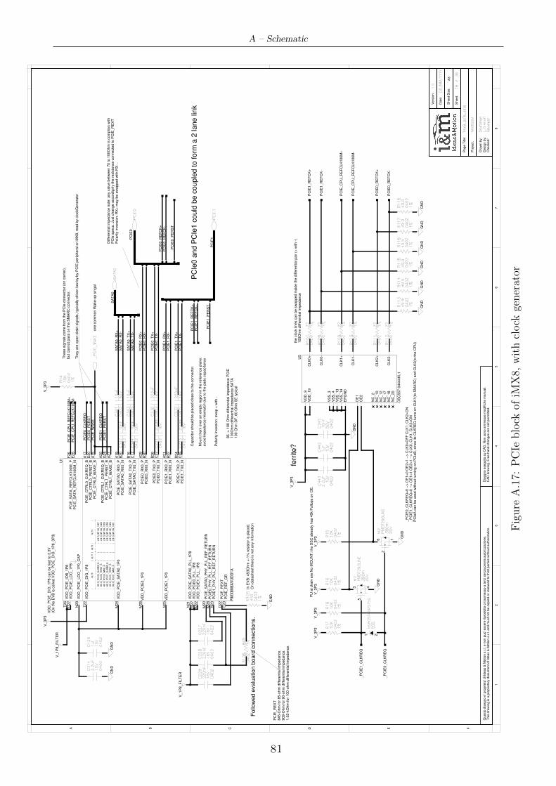
A – Schematic
PC
IE0
PC
IE1
SA
TA
0
PC
IE0
PC
IE1
SA
TA
0
PC
IE_C
TR
L0_C
LK
RE
Q_B
PC
IE_C
TR
L0_P
ER
ST
_B
PC
IE_C
TR
L0_W
AK
E_B
PC
IE_C
TR
L1_C
LK
RE
Q_B
PC
IE_C
TR
L1_P
ER
ST
_B
VD
D_P
CIE
_D
IG_1P
8
VD
D_P
CIE
_S
AT
A0_1P
0P
CIE
_S
AT
A0_R
X0_N
PC
IE_S
AT
A0_R
X0_P
PC
IE_S
AT
A0_T
X0_N
PC
IE_S
AT
A0_T
X0_P
PC
IE0_R
X0_N
PC
IE0_R
X0_P
PC
IE0_T
X0_N
PC
IE0_T
X0_P
VD
D_P
CIE
0_1P
0
PC
IE1_R
X0_N
PC
IE1_R
X0_P
PC
IE1_T
X0_N
PC
IE1_T
X0_P
VD
D_P
CIE
1_1P
0
PC
IE_S
AT
A0_P
HY
_P
LL_R
EF
_R
ET
UR
N
VD
D_P
CIE
_S
AT
A0_P
LL_1P
8
PC
IE1_P
HY
_P
LL_R
EF
_R
ET
UR
NP
CIE
0_P
HY
_P
LL_R
EF
_R
ET
UR
N
VD
D_P
CIE
0_P
LL_1P
8V
DD
_P
CIE
1_P
LL_1P
8
PC
IE_C
TR
L1_W
AK
E_B
PC
IE_R
EF
_Q
RP
CIE
_R
EX
T
PC
IE_S
AT
A_R
EF
CLK
100M
_N
PC
IE_S
AT
A_R
EF
CLK
100M
_P
VD
D_P
CIE
_IO
B_1P
8V
DD
_P
CIE
_LD
O_1P
8
VD
D_P
CIE
_LD
O_1P
0_C
AP
|
A
LT
0
|
AL
T1
|
A
LT
2
|
A
LT
3
|
+-
--
--
--
--
--
--
--
--
--
--
+-
--
--
-+
--
--
--
+-
--
--
--
--
--
--
--
--
+
|
HS
IO
_P
CI
E0
_C
LK
RE
Q_
B
|
|
|
LS
IO
_G
PI
O4
_I
O2
7
|
|
HS
IO
_P
CI
E0
_P
ER
ST
_B
|
|
|
LS
IO
_G
PI
O4
_I
O2
9
|
|
HS
IO
_P
CI
E0
_W
AK
E_
B
|
|
|
LS
IO
_G
PI
O4
_I
O2
8
|
|
HS
IO
_P
CI
E1
_C
LK
RE
Q_
B
|
|
|
LS
IO
_G
PI
O4
_I
O3
0
|
|
HS
IO
_P
CI
E1
_P
ER
ST
_B
|
|
|
LS
IO
_G
PI
O5
_I
O0
0
|
|
HS
IO
_P
CI
E1
_W
AK
E_
B
|
|
|
LS
IO
_G
PI
O4
_I
O3
1
|
U1
N29
U27
T26
F26
E25
D22
E23
A27
M22
N27
M28
N23
N21
M20
N25
B24
C25
A21
B22
M26
B26
C27
A29
B30
B16
C17
A19
B20
M24
T22
G25
A25
A15
D20
A17
PIM
X8M
6A
VU
DD
1A
SA
TA
0_R
X+
SA
TA
0_R
X-
SA
TA
0_T
X+
SA
TA
0_T
X-
PC
IE0_R
X+
PC
IE0_R
X-
PC
IE0_T
X+
PC
IE0_T
X-
PC
IE1_R
X+
PC
IE1_R
X-
PC
IE1_T
X+
PC
IE1_T
X-
PC
IE1_R
EF
CK
+P
CIE
1_R
EF
CK
-
_P
CIE
1_P
ER
ST
_P
CIE
_W
AK
E_P
CIE
_W
AK
E
_P
CIE
1_P
ER
ST
_P
CIE
0_P
ER
ST
one c
om
mon W
ake-u
p s
ingal
_P
CIE
0_C
LK
RE
Q
_P
CIE
1_C
LK
RE
Q
These s
ignals
com
e fro
m the P
CIe
connecto
r (o
n c
arr
ier)
,but cannot pass o
n the S
MA
RC
connecto
r.
They a
re o
pen-d
rain
sig
nals
, ty
pic
ally
driven low
by b
y P
CIE
periphera
l or
iMX
8, re
ad b
y c
lockG
enera
tor
V_1P
8_F
ILT
ER
V_1P
8_F
ILT
ER
V_3P
3
GN
D
In E
VB
: 453O
hm
+-1
% r
esis
tor
is p
laced.
On d
ata
sheet th
ere
is n
ot any info
rmation
Follo
wed e
valu
ation b
oard
connections.
GN
DG
ND
Dra
wn b
y:
Checked:
Desig
n b
y:
Pro
ject:
Sheet S
ize:
Page T
itle
:
Sheet:
Date
:
Vers
ion:
CA
D d
raw
ing. F
ree h
and c
hanges a
re n
ot perm
itte
d.
Dis
egno e
seguito s
u C
AD
. N
on s
ono a
mm
esse m
odific
he m
anuali.
This
dra
win
g is a
pro
prieta
ry d
ocum
ent of Id
eas &
Motion s
.r.l. and m
ust not be c
opie
d o
r re
leased to third p
art
ies w
ithout auth
orization.
Questo
dis
egno e
' pro
prieta
' di Id
eas &
Motion s
.r.l. e n
on p
uo' e
ssere
rip
rodotto o
tra
sm
esso a
terz
i senza p
revia
auto
rizzazio
ne.
/A3
12
34
56
78
A B C D E FiM
X8
SO
M
L.
Gir
au
di
18
36
1.0
DD
/M
M/
YY
YY
imx
8_
pc
ie_
sa
ta
Re
vie
we
r
Dra
ftm
an
VD
D_P
CIE
_D
IG_1P
8 c
an b
e tie
d to 3
.3V
(On the E
VB
is c
alle
d V
DD
_P
CIE
_D
IG_1P
8_3P
3)
PC
IE_R
EX
T845-O
hm
for
85-o
hm
diffe
rential im
pedance.
909-O
hm
for
90-o
hm
diffe
rential im
pedance.
1.0
2-k
Ohm
for
100-o
hm
diffe
rential im
pedance.
R1
05
04
02
45
3
1%
R1
06
04
02
84
51
%
C2
27
04
02
22
0n
F1
6V
16
V2
20
nF
04
02
C2
28
C2
29
04
02
22
0n
F1
6V
C1
26
04
02
1u
F1
0V
C3
14
04
02
2.2
uF
10
V
PC
IE_C
PU
_R
EF
CLK
100M
+P
CIE
_C
PU
_R
EF
CLK
100M
-
100O
hm
diffe
rential im
pedance
85 -
> 1
00 O
hm
diffe
rential im
pedance P
CIE
Capacitor
should
be p
laced c
lose to the c
onnecto
r.
C3
41
04
02
10
nF
50
VC
34
20
40
21
0n
F5
0V
50
V1
0n
F0
40
2C
34
3
50
V1
0n
F0
40
2C
34
4
16
V2
20
nF
04
02
C2
30
16
V2
20
nF
04
02
C2
31
16
V2
20
nF
04
02
C2
32
16
V2
20
nF
04
02
C2
33
Diffe
rential im
pedance n
ote
: any v
alu
e b
etw
een 7
0 to 1
00O
hm
is c
om
plia
n w
ith
PC
Ie s
pecs. Just change a
ccord
ignly
the r
esis
tance c
onnecte
d to P
CIE
_R
EX
TP
ola
rity
invers
ion: R
X+
may b
e s
wapped w
ith R
X-
.
PC
IE0_R
EF
CK
+P
CIE
0_R
EF
CK
-
_P
CIE
0_P
ER
ST
Mount th
em
over
an e
mpty
regio
n in the r
efe
rence p
lane:
avoid
im
pedance m
ism
atc
h d
ue to the p
ads c
apacitance
PC
Ie0 a
nd P
CIe
1 c
ould
be c
ouple
d to form
a 2
lane lin
k
100 O
hm
DF
, 60 O
hm
SE
typic
al
100O
hm
diffe
rential im
pedance S
AT
A
the c
lock lin
es c
an b
e s
wapped insid
e the d
iffe
rential pair (
+ w
ith -
)
VD
D_9
VD
D_19
VS
S_3
VS
S_4
VS
S_13
VS
S_14
NC
_2
NC
_10
NC
_12
NC
_17
NC
_18
NC
_20
OE
1O
E2
CLK
0+
CLK
0-
CLK
1+
CLK
1-
CLK
2+
CLK
2-
EP
GN
D
U5
DS
C557-0
4444K
L1
1%
22
04
02
R1
07
04
02
22
1%
R1
08
1%
22
04
02
R1
09
04
02
22
1%
R1
10
1%
22
04
02
R1
11
04
02
22
1%
R1
12
Pola
rity
invers
ion: sw
ap +
with -
R1
4
04
02
10
K
1%
V_3P
3
GN
D
1%
49
.90
40
2
R1
13
R1
14
04
02
49
.9
1%
GN
D
1%
49
.90
40
2
R1
15
GN
D
R1
16
04
02
49
.9
1%
GN
D
1%
49
.90
40
2
R1
17
GN
D
R1
18
04
02
49
.9
1%
GN
D
C3
45
04
02
10
nF
50
V
V_3P
3
PC
IE_C
PU
_R
EF
CLK
100M
+
PC
IE_C
PU
_R
EF
CLK
100M
-
PC
IE0_R
EF
CK
+
PC
IE0_R
EF
CK
-
PC
IE1_R
EF
CK
+
PC
IE1_R
EF
CK
-
M2
2
6 1
PM
DT2
90
UN
E3
80
m2
0V
M2
5
3 4
PM
DT2
90
UN
E3
80
m2
0V
GN
D
GN
D
_P
CIE
0_C
LK
RE
Q
_P
CIE
1_C
LK
RE
Q
R1
5
04
02
10
K
1%
1%
10
K0
40
2
R1
6
V_3P
3V
_3P
3
_P
CIE
0_C
LK
RE
Q=
0 -
-> O
E1=
0 O
E2=
1 -
-> C
LK
0=
OF
F C
LK
1, C
LK
2=
ON
_P
CIE
1_C
LK
RE
Q=
0 -
-> O
E1=
1 O
E2=
1 -
-> C
LK
0, C
LK
1, C
LK
2=
ON
PC
IeA
can b
e u
sed w
ithout tu
rnin
g o
n P
CIe
B, sin
ce its
CLK
RE
Q turn
s o
n C
LK
1(t
o S
MA
RC
) and C
LK
2(t
o the C
PU
)
R1
7
04
02
10
K
1%
1%
10
K0
40
2
R1
8
V_3P
3V
_3P
3
GN
D
1 2D
S5
NS
R0
5T4
0P
2T5
G
PU
at dra
in a
re N
o M
OU
NT
: th
e D
SC
already h
as 4
0k P
ullu
ps o
n O
E.
C4
42
04
02
1u
F1
0V
C4
43
04
02
2.2
uF
10
V
ferr
ite?
Figure
A.17:
PCIe
block
ofiM
X8,
withclock
generator
81
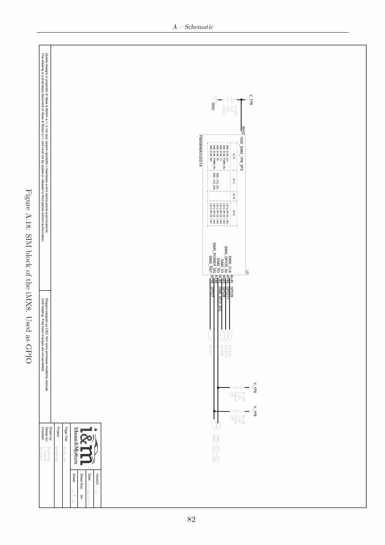
A – Schematic
Dra
wn b
y:
Checked:
Desig
n b
y:
Pro
ject:
Sheet S
ize:
Page T
itle:
Date
:
Vers
ion:
CA
D d
raw
ing. F
ree h
and c
hanges a
re n
ot p
erm
itted.
Dis
egno e
seguito
su C
AD
. Non s
ono a
mm
esse m
odific
he m
anuali.
This
dra
win
g is
a p
roprie
tary
docum
ent o
f Ideas &
Motio
n s
.r.l. and m
ust n
ot b
e c
opie
d o
r rele
ased to
third
partie
s w
ithout a
uth
oriz
atio
n.
Questo
dis
egno e
' pro
prie
ta' d
i Ideas &
Motio
n s
.r.l. e n
on p
uo' e
ssere
ripro
dotto
o tra
sm
esso a
terz
i senza p
revia
auto
rizzazio
ne.
Sheet:
/ A4
Re
vie
we
r
Dra
ftma
n
iMX
8S
OM
L. G
irau
di
19
36
1.0
DD
/M
M/
YY
YY
imx
8_
sim
SIM
0_C
LK
SIM
0_G
PIO
0_00
SIM
0_IO
SIM
0_P
DS
IM0_P
OW
ER
_E
NS
IM0_R
ST
VD
D_S
IM0_1P
8_3P
3+
--
--
--
--
--
--
--
--
--
-+
--
--
--
--
--
--
--
+-
--
--
-+
--
--
--
--
--
--
--
--
-+
|
AL
T0
|
AL
T1
|
A
LT
2
|
A
LT
3
|
+-
--
--
--
--
--
--
--
--
--
+-
--
--
--
--
--
--
-+
--
--
--
+-
--
--
--
--
--
--
--
--
+
|
DM
A_
SI
M0
_C
LK
|
|
|
LS
IO
_G
PI
O0
_I
O0
0
|
|
DM
A_
SI
M0
_P
OW
ER
_E
N
|
|
|
LS
IO
_G
PI
O0
_I
O0
5
|
|
DM
A_
SI
M0
_I
O
|
|
|
LS
IO
_G
PI
O0
_I
O0
2
|
|
DM
A_
SI
M0
_P
D
|
DM
A_
I2
C3
_S
CL
|
|
LS
IO
_G
PI
O0
_I
O0
3
|
|
DM
A_
SI
M0
_P
OW
ER
_E
N
|
DM
A_
I2
C3
_S
DA
|
|
LS
IO
_G
PI
O0
_I
O0
4
|
|
DM
A_
SI
M0
_R
ST
|
|
|
LS
IO
_G
PI
O0
_I
O0
1
|
+-
--
--
--
--
--
--
--
--
--
+-
--
--
--
--
--
--
-+
--
--
--
+-
--
--
--
--
--
--
--
--
+
U1
AK
42
AP
48
AT
48
AL43
AN
45
AP
46
AL45
PIM
X8M
6A
VU
DD
1A
V_1P
8
C1
38
04
02
1u
F1
0V
GN
DG
PIO
7
GP
IO8
GP
IO9
GP
IO1
1
GP
IO7
GP
IO8
GP
IO9
GP
IO11
DM
A_
I2C
3_
SD
AD
MA
_I2
C3
_S
CL
DM
A_I2
C3_S
CL
R1
25
04
02
2.2
K
1%
1%
2.2
K0
40
2
R1
26
V_1P
8V
_1P
8
Figu
reA.18:
SIM
block
oftheiM
X8.
Used
asGPIO
82
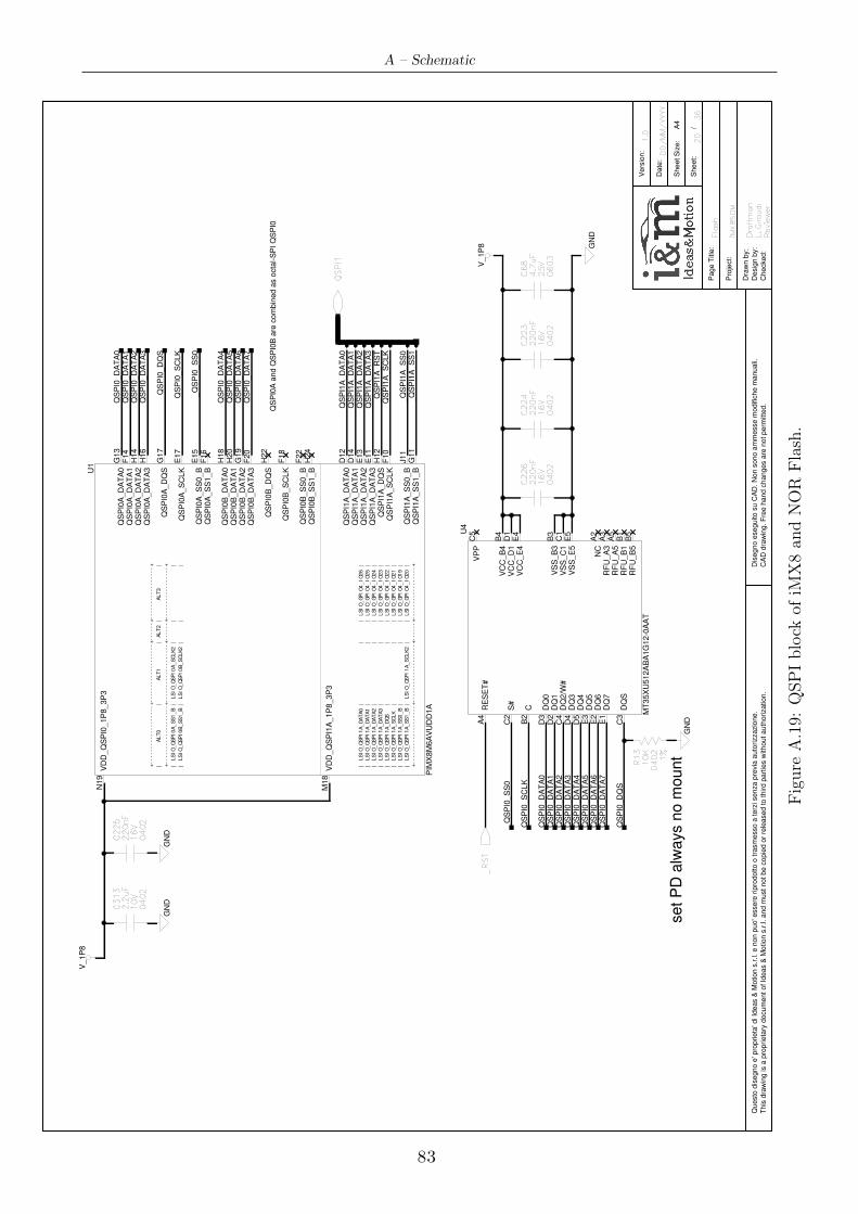
A – Schematic
QS
PI0
A_D
AT
A0
QS
PI0
A_D
AT
A1
QS
PI0
A_D
AT
A2
QS
PI0
A_D
AT
A3
QS
PI0
A_D
QS
QS
PI0
A_S
CLK
QS
PI0
A_S
S0_B
QS
PI0
A_S
S1_B
QS
PI0
B_D
AT
A0
QS
PI0
B_D
AT
A1
QS
PI0
B_D
AT
A2
QS
PI0
B_D
AT
A3
QS
PI0
B_D
QS
QS
PI0
B_S
CLK
QS
PI0
B_S
S0_B
QS
PI0
B_S
S1_B
QS
PI1
A_D
AT
A0
QS
PI1
A_D
AT
A1
QS
PI1
A_D
AT
A2
QS
PI1
A_D
AT
A3
QS
PI1
A_D
QS
QS
PI1
A_S
CLK
QS
PI1
A_S
S0_B
QS
PI1
A_S
S1_B
VD
D_Q
SP
I0_1P
8_3P
3
VD
D_Q
SP
I1A
_1P
8_3P
3
+-
--
--
--
--
--
--
--
--
--
+-
--
--
--
--
--
--
--
--
--
+-
--
--
-+
--
--
--
--
--
--
--
--
-+
|
AL
T0
|
AL
T1
|
AL
T2
|
AL
T3
|
+-
--
--
--
--
--
--
--
--
--
+-
--
--
--
--
--
--
--
--
--
+-
--
--
-+
--
--
--
--
--
--
--
--
-+
|
LS
IO
_Q
SP
I0
A_
SS
1_
B
|
LS
IO
_Q
SP
I0
A_
SC
LK
2
|
|
|
|
LS
IO
_Q
SP
I0
B_
SS
1_
B
|
LS
IO
_Q
SP
I0
B_
SC
LK
2
|
|
|
|
LS
IO
_Q
SP
I1
A_
DA
TA
0
|
|
|
L
SI
O_
GP
IO
4_
IO
26
|
|
LS
IO
_Q
SP
I1
A_
DA
TA
1
|
|
|
L
SI
O_
GP
IO
4_
IO
25
|
|
LS
IO
_Q
SP
I1
A_
DA
TA
2
|
|
|
L
SI
O_
GP
IO
4_
IO
24
|
|
LS
IO
_Q
SP
I1
A_
DA
TA
3
|
|
|
L
SI
O_
GP
IO
4_
IO
23
|
|
LS
IO
_Q
SP
I1
A_
DQ
S
|
|
|
L
SI
O_
GP
IO
4_
IO
22
|
|
LS
IO
_Q
SP
I1
A_
SC
LK
|
|
|
L
SI
O_
GP
IO
4_
IO
21
|
|
LS
IO
_Q
SP
I1
A_
SS
0_
B
|
|
|
L
SI
O_
GP
IO
4_
IO
19
|
|
LS
IO
_Q
SP
I1
A_
SS
1_
B
|
LS
IO
_Q
SP
I1
A_
SC
LK
2
|
|
L
SI
O_
GP
IO
4_
IO
20
|
+-
--
--
--
--
--
--
--
--
--
+-
--
--
--
--
--
--
--
--
--
+-
--
--
-+
--
--
--
--
--
--
--
--
-+
U1
PIM
X8M
6A
VU
DD
1A
M18
N19
G11
J11
F10
H12
E11
E13
D14
D12
H24
F22
F18
H22
F20
G19
H20
H18
F16
E15
E17
G17
H16
H14
F14
G13
DQ
0D
Q1
DQ
2/W
#D
Q3
DQ
4D
Q5
DQ
6
DQ
S
DQ
7
RE
SE
T#
RF
U_A
3R
FU
_A
5R
FU
_B
1R
FU
_B
5
S#
C
NC
VS
S_C
1V
SS
_B
3
VS
S_E
5
VC
C_B
4V
CC
_D
1V
CC
_E
4
VP
P
D3
D2
C4
D4
D5
E3
E2
C3
E1
A4
A3
A5
B1
B5
C2
B2
A2
C1
B3
E5
B4
D1
E4
C5
MT
35X
U512A
BA
1G
12-0
AA
T
U4
Dra
wn b
y:
Checked:
Desig
n b
y:
Pro
ject:
Sheet S
ize:
Page T
itle
:
Date
:
Vers
ion:
CA
D d
raw
ing. F
ree h
and c
hanges a
re n
ot perm
itte
d.
Dis
egno e
seguito s
u C
AD
. N
on s
ono a
mm
esse m
odific
he m
anuali.
This
dra
win
g is a
pro
prieta
ry d
ocum
ent of Id
eas &
Motion s
.r.l. and m
ust not be c
opie
d o
r re
leased to third p
art
ies w
ithout auth
orization.
Questo
dis
egno e
' pro
prieta
' di Id
eas &
Motion s
.r.l. e n
on p
uo' e
ssere
rip
rodotto o
tra
sm
esso a
terz
i senza p
revia
auto
rizzazio
ne.
Sheet:
/A4
iMX
8S
OM
L.
Gir
au
di
20
36
1.0
DD
/M
M/
YY
YY
Fla
sh
Re
vie
we
r
Dra
ftm
an
16
V2
20
nF
04
02
C2
23
C2
24
04
02
22
0n
F1
6VQ
SP
I0_D
AT
A0
QS
PI0
_D
AT
A1
QS
PI0
_D
AT
A2
QS
PI0
_D
AT
A3
QS
PI0
_D
AT
A4
QS
PI0
_D
AT
A5
QS
PI0
_D
AT
A6
QS
PI0
_D
AT
A7
QS
PI0
_D
QS
QS
PI0
_S
CLK
_Q
SP
I0_S
S0
_Q
SP
I0_S
S0
QS
PI0
_S
CLK
_R
ST
QS
PI1
A_D
AT
A0
QS
PI1
A_D
AT
A1
QS
PI1
A_D
AT
A2
QS
PI1
A_D
AT
A3
_Q
SP
I1A
_R
ST
QS
PI1
A_S
CLK
_Q
SP
I1A
_S
S1
QS
PI1
QS
PI0
A a
nd Q
SP
I0B
are
com
bin
ed a
s o
cta
l-S
PI Q
SP
I0
set P
D a
lways n
o m
ount
_Q
SP
I1A
_S
S0
C2
25
04
02
22
0n
F1
6V
GN
DG
ND
04
02
C3
13
2.2
uF
10
V
V_1P
8
R1
31
0K
1%
04
02
QS
PI0
_D
AT
A0
QS
PI0
_D
AT
A1
QS
PI0
_D
AT
A2
QS
PI0
_D
AT
A3
QS
PI0
_D
AT
A4
QS
PI0
_D
AT
A5
QS
PI0
_D
AT
A6
QS
PI0
_D
AT
A7
GN
D
V_1P
8
QS
PI0
_D
QS
GN
D
25
V4
.7u
F
06
03
C6
8
16
V2
20
nF
04
02
C2
26
Figure
A.19:
QSPIblock
ofiM
X8an
dNOR
Flash.
83
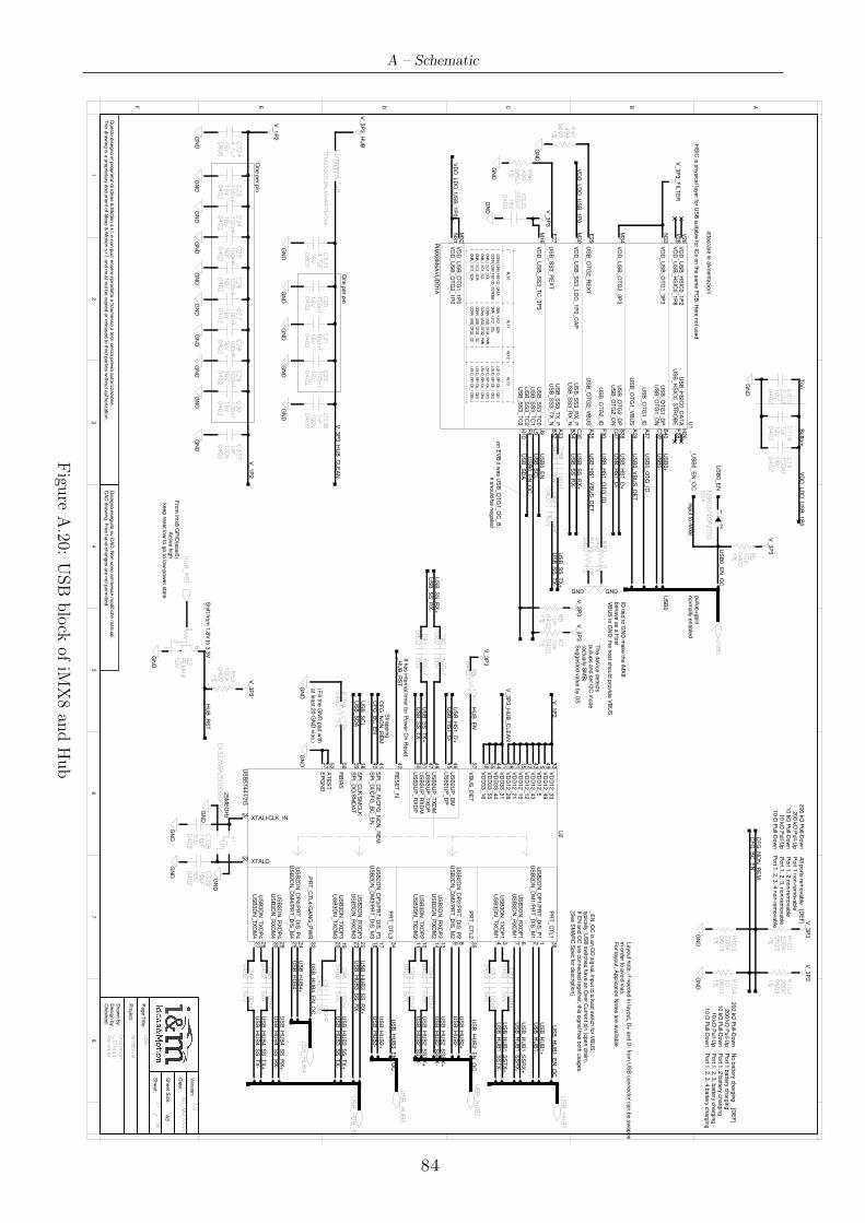
A – Schematic
PR
T_C
TL1
PR
T_C
TL2
PR
T_C
TL3
PR
T_C
TL4/G
AN
G_P
WR
US
B2D
N_D
M1/P
RT
_D
IS_M
1
US
B2D
N_D
M2/P
RT
_D
IS_M
2
US
B2D
N_D
M3/P
RT
_D
IS_M
3
US
B2D
N_D
M4/P
RT
_D
IS_M
4
US
B2D
N_D
P1/P
RT
_D
IS_P
1
US
B2D
N_D
P2/P
RT
_D
IS_P
2
US
B2D
N_D
P3/P
RT
_D
IS_P
3
US
B2D
N_D
P4/P
RT
_D
IS_P
4
US
B3D
N_R
XD
M1
US
B3D
N_R
XD
M2
US
B3D
N_R
XD
M3
US
B3D
N_R
XD
M4
US
B3D
N_R
XD
P1
US
B3D
N_R
XD
P2
US
B3D
N_R
XD
P3
US
B3D
N_R
XD
P4
US
B3D
N_T
XD
M1
US
B3D
N_T
XD
M2
US
B3D
N_T
XD
M3
US
B3D
N_T
XD
M4
US
B3D
N_T
XD
P1
US
B3D
N_T
XD
P2
US
B3D
N_T
XD
P3
US
B3D
N_T
XD
P4
AT
ES
TE
PG
ND
RB
IAS
RE
SE
T_N
SP
I_C
E_N
/CF
G_N
ON
_R
EM
SP
I_C
LK
/SM
CLK
SP
I_D
I/CF
G_B
C_E
N
SP
I_D
O/S
MD
AT
US
B2U
P_D
MU
SB
2U
P_D
P
US
B3U
P_R
XD
MU
SB
3U
P_R
XD
P
US
B3U
P_T
XD
MU
SB
3U
P_T
XD
P
VB
US
_D
ET
VD
D12_33
VD
D12_49
VD
D12_5
VD
D12_43
VD
D12_12
VD
D12_15
VD
D12_21
VD
D12_28
VD
D33_31
VD
D33_44
VD
D33_55
VD
D33_16
XTALI/CLK_IN
XTALO
U2
53
16
55
44
31
28
21
15
12
43 5
49
33
37
47
48
50
51
45
46
39
40
38
41
42
56
57
52
26
19
10
327
20
11
429
22
13
630
23
14
724
17
8 125
18
9 232
34
35
36
US
B5744-I/2
G
Dra
wn b
y:
Checked:
Desig
n b
y:
Pro
ject:
Sheet S
ize:
Page T
itle:
Sheet:
Date
:
Vers
ion:
CA
D d
raw
ing. F
ree h
and c
hanges a
re n
ot p
erm
itted.
Dis
egno e
seguito
su C
AD
. Non s
ono a
mm
esse m
odific
he m
anuali.
This
dra
win
g is
a p
roprie
tary
docum
ent o
f Ideas &
Motio
n s
.r.l. and m
ust n
ot b
e c
opie
d o
r rele
ased to
third
partie
s w
ithout a
uth
oriz
atio
n.
Questo
dis
egno e
' pro
prie
ta' d
i Ideas &
Motio
n s
.r.l. e n
on p
uo' e
ssere
ripro
dotto
o tra
sm
esso a
terz
i senza p
revia
auto
rizzazio
ne.
/ A3
12
34
56
78
ABCDEF
Re
vie
we
r
Dra
ftma
n
iMX
8S
OM
L. G
irau
di
21
36
1.0
DD
/M
M/
YY
YY
US
B
US
B_H
SIC
0_D
AT
AU
SB
_H
SIC
0_S
TR
OB
EV
DD
_U
SB
_H
SIC
0_1P
2V
DD
_U
SB
_H
SIC
0_1P
8
VD
D_U
SB
_O
TG
1_1P
0
VD
D_U
SB
_O
TG
1_3P
3U
SB
_O
TG
1_D
NU
SB
_O
TG
1_D
P
US
B_O
TG
1_ID
US
B_O
TG
1_V
BU
S
VD
D_U
SB
_O
TG
2_1P
0
VD
D_U
SB
_O
TG
2_3P
3U
SB
_O
TG
2_D
NU
SB
_O
TG
2_D
P
US
B_O
TG
2_ID
US
B_O
TG
2_V
BU
SU
SB
_O
TG
2_R
EX
T
VD
D_U
SB
_S
S3_LD
O_1P
0_C
AP
VD
D_U
SB
_S
S3_T
C_3P
3
US
B_S
S3_R
EX
T
US
B_S
S3_R
X_N
US
B_S
S3_R
X_P
US
B_S
S3_T
C0
US
B_S
S3_T
C1
US
B_S
S3_T
C2
US
B_S
S3_T
C3
US
B_S
S3_T
X_N
US
B_S
S3_T
X_P
+-
--
--
--
--
--
--
--
--
--
--
--
+-
--
--
--
--
--
--
--
--
--
+-
--
--
-+
--
--
--
--
--
--
--
--
-+
|
AL
T0
|
AL
T1
|
AL
T2
|
AL
T3
|
+-
--
--
--
--
--
--
--
--
--
--
--
+-
--
--
--
--
--
--
--
--
--
+-
--
--
-+
--
--
--
--
--
--
--
--
-+
|
CO
NN
_U
SB
_H
SI
C0
_D
AT
A
|
DM
A_
I2
C1
_S
DA
|
|
L
SI
O_
GP
IO
5_
IO
01
|
|
CO
NN
_U
SB
_H
SI
C0
_S
TR
OB
E
|
DM
A_
I2
C1
_S
CL
|
|
L
SI
O_
GP
IO
5_
IO
02
|
|
DM
A_
I2
C1
_S
CL
|
CO
NN
_U
SB
_O
TG
1_
PW
R
|
|
L
SI
O_
GP
IO
4_
IO
03
|
|
DM
A_
I2
C1
_S
CL
|
CO
NN
_U
SB
_O
TG
2_
PW
R
|
|
L
SI
O_
GP
IO
4_
IO
04
|
|
DM
A_
I2
C1
_S
DA
|
CO
NN
_U
SB
_O
TG
1_
OC
|
|
L
SI
O_
GP
IO
4_
IO
05
|
|
DM
A_
I2
C1
_S
DA
|
CO
NN
_U
SB
_O
TG
2_
OC
|
|
L
SI
O_
GP
IO
4_
IO
06
|
+-
--
--
--
--
--
--
--
--
--
--
--
+-
--
--
--
--
--
--
--
--
--
+-
--
--
-+
--
--
--
--
--
--
--
--
-+
U1
A33
B32
H10
F8
L9
J9
C35
B34
E27
M16
M30
E29
A35
F30
B38
C37
M34
N31
A39
A37
B40
C39
N33
M32
V28
V26
F28
H26
PIM
X8M
6A
VU
DD
1A
US
B_
HU
B2
US
B_
HU
B4
US
B0
US
B_
HU
B3
US
B0
V_3P
3
GN
D
GN
D
Botto
mT
opGN
D
VD
D_LD
O_U
SB
_1P
0
VD
D_LD
O_U
SB
_1P
0
V_3P
3_F
ILT
ER
Layout n
ote
: if needed in
layout, D
+ a
nd D
- from
US
B c
onnecto
r can b
e s
wapped
in o
rder to
avoid
via
s.
For la
yout, A
pplic
atio
n N
ote
s a
re a
vaila
ble
V_3P
3_H
UB
_C
LE
AN
V_3P
3_H
UB
_C
LE
AN
V_3P
3_H
UB
One p
er p
in
GN
DG
ND
GN
DG
ND
GN
D
V_1P
2
GN
DG
ND
GN
DG
ND
GN
DG
ND
GN
DG
ND
One p
er p
in
GN
DG
ND
HU
B_E
N
(Fill th
e G
ND
pad w
ithat le
ast 2
0 G
ND
via
s.)
GN
D
_H
UB
_R
ST
GN
D
4.7
uH
TF
M2
52
01
2A
LM
A4
R7
MTA
A
L1
16
V4
.7u
F
08
05
C3
33
16
V1
00
nF
04
02
C2
0
04
02
10
0n
F1
6V
C2
1
10
0V
C3
36
04
02
1n
FC
22
04
02
10
0n
F1
6V
C2
3
04
02
10
0n
F1
6V
16
V1
00
nF
04
02
C2
8
16
V1
00
nF
04
02
C2
7
16
V1
00
nF
04
02
C2
5
16
V1
00
nF
04
02
C2
4
16
V1
00
nF
04
02
C2
6
16
V1
00
nF
04
02
C2
9
16
V1
00
nF
04
02
C3
0C
33
4
08
05
4.7
uF
16
V
C3
37
04
02
1n
F1
00
V
R1
00
04
02
12
K1
%
R9
6
06
03
49
9
1%
R9
7
06
03
49
9
1%
C1
9
04
02
10
0n
F1
6V
C1
19
04
02
1u
F1
0V
C3
10
04
02
2.2
uF
10
V
Stra
ppin
g
US
B_S
CL
US
B_S
DA
US
B_S
CL
US
B_S
DA
V_3P
3V
_3P
3
_U
SB
0_E
N_O
C
US
B_H
UB
3+
US
B_H
UB
3-
_U
SB
_H
UB
3_E
N_O
C
US
B_H
UB
1+
US
B_H
UB
1-
_U
SB
_H
UB
1_E
N_O
C
US
B_H
UB
1_S
SR
X+
US
B_H
UB
1_S
SR
X-
US
B_H
UB
1_S
ST
X+
US
B_H
UB
1_S
ST
X-
US
B_H
UB
2+
US
B_H
UB
2-
_U
SB
_H
UB
2_E
N_O
C
US
B_H
UB
2_S
SR
X+
US
B_H
UB
2_S
SR
X-
US
B_H
UB
2_S
ST
X+
US
B_H
UB
2_S
ST
X-
US
B_H
S1_D
+U
SB
_H
S1_D
-
US
B_H
S1_O
TG
_ID
US
B_H
S1_V
BU
S_D
ET
US
B_S
S_R
X+
US
B_S
S_R
X-
US
B_S
S_T
X+
US
B_S
S_T
X-
US
B_H
S1_D
+U
SB
_H
S1_D
-
US
B_S
S_R
X+
US
B_S
S_R
X-
US
B_S
S_T
X+
US
B_S
S_T
X-
CF
G_N
ON
_R
EM
CF
G_B
C_E
N
CF
G_N
ON
_R
EM
CF
G_B
C_E
N
200 k
O P
ull-D
ow
n200 k
O P
ull-U
p10 k
O P
ull-D
ow
n10 k
O P
ull-U
p10 O
Pull-D
ow
n
All p
orts
rem
ovable
[DE
F]
Port 1
non-re
movable
Port 1
, 2 n
on-re
movable
Port 1
, 2, 3
, non-re
movable
Port 1
, 2, 3
, 4 n
on-re
movable
200 k
O P
ull-D
ow
n200 k
O P
ull-U
p10 k
O P
ull-D
ow
n10 k
O P
ull-U
p10 O
Pull-D
ow
n
No b
atte
ry c
harg
ing [D
EF
]P
ort 1
batte
ry c
harg
ing
Port 1
, 2 b
atte
ry c
harg
ing
Port 1
, 2, 3
, batte
ry c
harg
ing
Port 1
, 2, 3
, 4 b
atte
ry c
harg
ing
R1
01
06
03
20
0K
1%
V_3P
3GN
DG
ND
R1
02
06
03
20
0K
1%
R1
04
06
03
10
1%
V_3P
3
1%
20
0K
06
03
R1
03
_U
SB
0_E
N_O
C
on E
VB
it was U
SB
_O
TG
1_O
C_B
:it s
hould
be n
egate
d
US
B0+
US
B0-
V_1P
2
V_1P
2
VD
D_LD
O_U
SB
_1P
0
R5
04
02
10
K
1%
V_3P
3
pullu
p+
gpio
norm
ally
enable
d
US
B0_E
N
US
B0_O
TG
_ID
US
B0_V
BU
S_D
ET
GN
DG
ND
GN
D
GN
D
Y1
CX
32
25
SA
25
00
0D
0P
TV
CC
25M
EG
Hz
50
V1
6p
F
04
02
C3
38
50
V1
6p
F
04
02
C3
39
US
B_H
UB
3_S
S_R
X+
US
B_H
UB
3_S
S_R
X-
US
B_H
UB
3_S
S_T
X+
US
B_H
UB
3_S
S_T
X-
US
B_H
UB
4_S
S_R
X+
US
B_H
UB
4_S
S_R
X-
US
B_H
UB
4_S
S_T
X+
US
B_H
UB
4_S
S_T
X-
The d
evic
e d
ete
cts
pullu
ps a
nd s
et I2
C m
ode
(actu
ally
SM
B)
Suggeste
d v
alu
e b
y D
S
It has in
tern
al tim
er fo
r Pow
er O
n R
eset
54
_U
SB
_H
UB
4_E
N_O
C
US
B_H
UB
4+
US
B_H
UB
4-
R5
2
04
02
10
0K
1% V
_3P
3
HU
B_
RS
T
Fro
m im
x8 G
PIO
(esai0
)A
ctiv
e h
igh
HS
IC is
physic
al la
yer fo
r US
B s
uita
ble
for IC
s o
n th
e s
am
e P
CB
. Here
not u
sed
_E
N_O
C is
an O
D s
ignal, in
put to
a lo
ad s
witc
h fo
r VB
US
: ty
pic
ally
, US
B s
witc
hes h
ave a
n O
ver C
urre
nt p
in (o
pen d
rain
). If E
N a
nd O
C a
re c
onnecte
d to
geth
er, th
is s
ignal h
as b
oth
usages.
[See S
MA
RC
Spec fo
r descrip
tion]
R6
04
02
10
K
1%
1%
10
K0
40
2
R7
C8
80
40
21
00
nF
50
VC
89
04
02
10
0n
F5
0V
C9
00
40
21
00
nF
50
V
_H
UB
_R
ST
C9
10
40
21
00
nF
50
V
C9
20
40
21
00
nF
50
V
C9
30
40
21
00
nF
50
V
C9
40
40
21
00
nF
50
V
C9
50
40
21
00
nF
50
V
C9
60
40
21
00
nF
50
V
C9
70
40
21
00
nF
50
V
C9
80
40
21
00
nF
50
V
C9
90
40
21
00
nF
50
V
atta
ccare
le a
limenta
zio
ni
Q2
1 6
2P
EM
H9
50
V
GN
D
R8
04
02
10
K1
%
V_3P
3
US
B_
HU
B_
SS
keep re
set lo
w to
go to
low
-pow
er s
tate
DS
4
2
1
NS
R0
5T4
0P
2T5
G
US
B0_E
N
_U
SB
0_E
N_O
CIn
put to
iMX
8
US
B_
HU
B1
GN
D
C2
22
04
02
22
0n
F1
6V
R8
20
40
201
%
GND
ID tie
d to
GN
D m
ake th
e iM
X8
behave a
s a
Host
VB
US
to G
ND
: the h
ost s
hould
pro
vid
e V
BU
S
Shift fro
m 1
.8V
to 3
.3V
R1
53
04
02
10
K1
%
GND
Figu
reA.20:
USB
block
ofiM
X8an
dHub
84
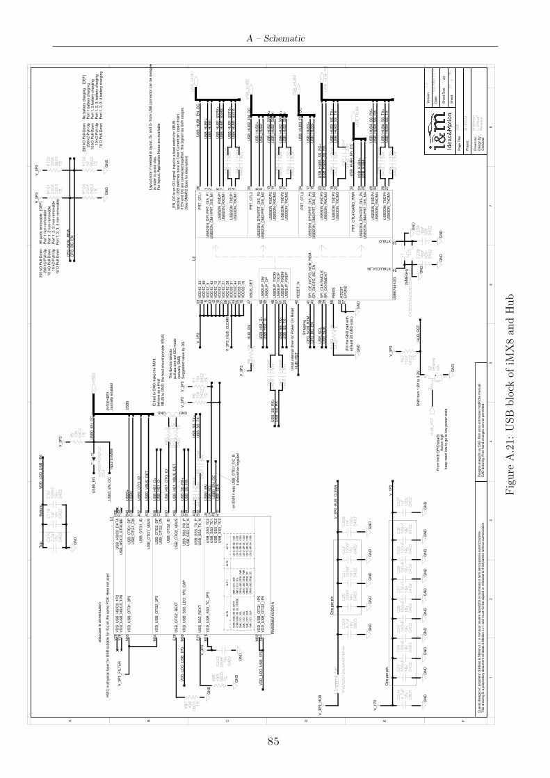
A – Schematic
PR
T_C
TL1
PR
T_C
TL2
PR
T_C
TL3
PR
T_C
TL4/G
AN
G_P
WR
US
B2D
N_D
M1/P
RT
_D
IS_M
1
US
B2D
N_D
M2/P
RT
_D
IS_M
2
US
B2D
N_D
M3/P
RT
_D
IS_M
3
US
B2D
N_D
M4/P
RT
_D
IS_M
4
US
B2D
N_D
P1/P
RT
_D
IS_P
1
US
B2D
N_D
P2/P
RT
_D
IS_P
2
US
B2D
N_D
P3/P
RT
_D
IS_P
3
US
B2D
N_D
P4/P
RT
_D
IS_P
4
US
B3D
N_R
XD
M1
US
B3D
N_R
XD
M2
US
B3D
N_R
XD
M3
US
B3D
N_R
XD
M4
US
B3D
N_R
XD
P1
US
B3D
N_R
XD
P2
US
B3D
N_R
XD
P3
US
B3D
N_R
XD
P4
US
B3D
N_T
XD
M1
US
B3D
N_T
XD
M2
US
B3D
N_T
XD
M3
US
B3D
N_T
XD
M4
US
B3D
N_T
XD
P1
US
B3D
N_T
XD
P2
US
B3D
N_T
XD
P3
US
B3D
N_T
XD
P4
AT
ES
TE
PG
ND
RB
IAS
RE
SE
T_N
SP
I_C
E_N
/CF
G_N
ON
_R
EM
SP
I_C
LK
/SM
CLK
SP
I_D
I/C
FG
_B
C_E
N
SP
I_D
O/S
MD
AT
US
B2U
P_D
MU
SB
2U
P_D
P
US
B3U
P_R
XD
MU
SB
3U
P_R
XD
P
US
B3U
P_T
XD
MU
SB
3U
P_T
XD
P
VB
US
_D
ET
VD
D12_33
VD
D12_49
VD
D12_5
VD
D12_43
VD
D12_12
VD
D12_15
VD
D12_21
VD
D12_28
VD
D33_31
VD
D33_44
VD
D33_55
VD
D33_16
XTALI/CLK_IN
XTALO
U2
53
16
55
44
31
28
21
15
12
435
49
33
37
47
48
50
51
45
46
39
40
38
41
42
56
57
52
26
19
10
3 27
20
11
4 29
22
13
6 30
23
14
7 24
17
81 25
18
92 32
34
35
36
US
B5744-I
/2G
Dra
wn b
y:
Checked:
Desig
n b
y:
Pro
ject:
Sheet S
ize:
Page T
itle
:
Sheet:
Date
:
Vers
ion:
CA
D d
raw
ing. F
ree h
and c
hanges a
re n
ot perm
itte
d.
Dis
egno e
seguito s
u C
AD
. N
on s
ono a
mm
esse m
odific
he m
anuali.
This
dra
win
g is a
pro
prieta
ry d
ocum
ent of Id
eas &
Motion s
.r.l. and m
ust not be c
opie
d o
r re
leased to third p
art
ies w
ithout auth
orization.
Questo
dis
egno e
' pro
prieta
' di Id
eas &
Motion s
.r.l. e n
on p
uo' e
ssere
rip
rodotto o
tra
sm
esso a
terz
i senza p
revia
auto
rizzazio
ne.
/A3
12
34
56
78
A B C D E F
Re
vie
we
r
Dra
ftm
an
iMX
8S
OM
L.
Gir
au
di
21
36
1.0
DD
/M
M/
YY
YY
US
B
US
B_H
SIC
0_D
AT
AU
SB
_H
SIC
0_S
TR
OB
EV
DD
_U
SB
_H
SIC
0_1P
2V
DD
_U
SB
_H
SIC
0_1P
8
VD
D_U
SB
_O
TG
1_1P
0
VD
D_U
SB
_O
TG
1_3P
3U
SB
_O
TG
1_D
NU
SB
_O
TG
1_D
P
US
B_O
TG
1_ID
US
B_O
TG
1_V
BU
S
VD
D_U
SB
_O
TG
2_1P
0
VD
D_U
SB
_O
TG
2_3P
3U
SB
_O
TG
2_D
NU
SB
_O
TG
2_D
P
US
B_O
TG
2_ID
US
B_O
TG
2_V
BU
SU
SB
_O
TG
2_R
EX
T
VD
D_U
SB
_S
S3_LD
O_1P
0_C
AP
VD
D_U
SB
_S
S3_T
C_3P
3
US
B_S
S3_R
EX
T
US
B_S
S3_R
X_N
US
B_S
S3_R
X_P
US
B_S
S3_T
C0
US
B_S
S3_T
C1
US
B_S
S3_T
C2
US
B_S
S3_T
C3
US
B_S
S3_T
X_N
US
B_S
S3_T
X_P
+-
--
--
--
--
--
--
--
--
--
--
--
+-
--
--
--
--
--
--
--
--
--
+-
--
--
-+
--
--
--
--
--
--
--
--
-+
|
AL
T0
|
AL
T1
|
AL
T2
|
AL
T3
|
+-
--
--
--
--
--
--
--
--
--
--
--
+-
--
--
--
--
--
--
--
--
--
+-
--
--
-+
--
--
--
--
--
--
--
--
-+
|
CO
NN
_U
SB
_H
SI
C0
_D
AT
A
|
DM
A_
I2
C1
_S
DA
|
|
L
SI
O_
GP
IO
5_
IO
01
|
|
CO
NN
_U
SB
_H
SI
C0
_S
TR
OB
E
|
DM
A_
I2
C1
_S
CL
|
|
L
SI
O_
GP
IO
5_
IO
02
|
|
DM
A_
I2
C1
_S
CL
|
CO
NN
_U
SB
_O
TG
1_
PW
R
|
|
L
SI
O_
GP
IO
4_
IO
03
|
|
DM
A_
I2
C1
_S
CL
|
CO
NN
_U
SB
_O
TG
2_
PW
R
|
|
L
SI
O_
GP
IO
4_
IO
04
|
|
DM
A_
I2
C1
_S
DA
|
CO
NN
_U
SB
_O
TG
1_
OC
|
|
L
SI
O_
GP
IO
4_
IO
05
|
|
DM
A_
I2
C1
_S
DA
|
CO
NN
_U
SB
_O
TG
2_
OC
|
|
L
SI
O_
GP
IO
4_
IO
06
|
+-
--
--
--
--
--
--
--
--
--
--
--
+-
--
--
--
--
--
--
--
--
--
+-
--
--
-+
--
--
--
--
--
--
--
--
-+
U1
A33
B32
H10
F8
L9
J9
C35
B34
E27
M16
M30
E29
A35
F30
B38
C37
M34
N31
A39
A37
B40
C39
N33
M32
V28
V26
F28
H26
PIM
X8M
6A
VU
DD
1A
US
B_
HU
B2
US
B_
HU
B4
US
B0
US
B_
HU
B3
US
B0
V_3P
3
GN
D
GN
D
Bottom
Top GN
D
VD
D_LD
O_U
SB
_1P
0
VD
D_LD
O_U
SB
_1P
0
V_3P
3_F
ILT
ER
Layout note
: if n
eeded in layout, D
+ a
nd D
- fr
om
US
B c
onnecto
r can b
e s
wapped
in o
rder
to a
void
via
s.
For
layout, A
pplic
ation N
ote
s a
re a
vaila
ble
V_3P
3_H
UB
_C
LE
AN
V_3P
3_H
UB
_C
LE
AN
V_3P
3_H
UB
One p
er
pin
GN
DG
ND
GN
DG
ND
GN
D
V_1P
2
GN
DG
ND
GN
DG
ND
GN
DG
ND
GN
DG
ND
One p
er
pin
GN
DG
ND
HU
B_E
N
(Fill
the G
ND
pad w
ith
at le
ast 20 G
ND
via
s.)
GN
D
_H
UB
_R
ST
GN
D
4.7
uH
TF
M2
52
01
2A
LM
A4
R7
MTA
A
L1
16
V4
.7u
F
08
05
C3
33
16
V1
00
nF
04
02
C2
0
04
02
10
0n
F1
6V
C2
1
10
0V
C3
36
04
02
1n
FC
22
04
02
10
0n
F1
6V
C2
3
04
02
10
0n
F1
6V
16
V1
00
nF
04
02
C2
8
16
V1
00
nF
04
02
C2
7
16
V1
00
nF
04
02
C2
5
16
V1
00
nF
04
02
C2
4
16
V1
00
nF
04
02
C2
6
16
V1
00
nF
04
02
C2
9
16
V1
00
nF
04
02
C3
0C
33
4
08
05
4.7
uF
16
V
C3
37
04
02
1n
F1
00
V
R1
00
04
02
12
K1
%
R9
6
06
03
49
9
1%
R9
7
06
03
49
9
1%
C1
9
04
02
10
0n
F1
6V
C1
19
04
02
1u
F1
0V
C3
10
04
02
2.2
uF
10
V
Str
appin
g
US
B_S
CL
US
B_S
DA
US
B_S
CL
US
B_S
DA
V_3P
3V
_3P
3
_U
SB
0_E
N_O
C
US
B_H
UB
3+
US
B_H
UB
3-
_U
SB
_H
UB
3_E
N_O
C
US
B_H
UB
1+
US
B_H
UB
1-
_U
SB
_H
UB
1_E
N_O
C
US
B_H
UB
1_S
SR
X+
US
B_H
UB
1_S
SR
X-
US
B_H
UB
1_S
ST
X+
US
B_H
UB
1_S
ST
X-
US
B_H
UB
2+
US
B_H
UB
2-
_U
SB
_H
UB
2_E
N_O
C
US
B_H
UB
2_S
SR
X+
US
B_H
UB
2_S
SR
X-
US
B_H
UB
2_S
ST
X+
US
B_H
UB
2_S
ST
X-
US
B_H
S1_D
+U
SB
_H
S1_D
-
US
B_H
S1_O
TG
_ID
US
B_H
S1_V
BU
S_D
ET
US
B_S
S_R
X+
US
B_S
S_R
X-
US
B_S
S_T
X+
US
B_S
S_T
X-
US
B_H
S1_D
+U
SB
_H
S1_D
-
US
B_S
S_R
X+
US
B_S
S_R
X-
US
B_S
S_T
X+
US
B_S
S_T
X-
CF
G_N
ON
_R
EM
CF
G_B
C_E
N
CF
G_N
ON
_R
EM
CF
G_B
C_E
N
200 k
O P
ull-
Dow
n200 k
O P
ull-
Up
10 k
O P
ull-
Dow
n10 k
O P
ull-
Up
10 O
Pull-
Dow
n
All
port
s r
em
ovable
[D
EF
] P
ort
1 n
on-r
em
ovable
Port
1, 2 n
on-r
em
ovable
Port
1, 2, 3, non-r
em
ovable
Port
1, 2, 3, 4 n
on-r
em
ovable
200 k
O P
ull-
Dow
n200 k
O P
ull-
Up
10 k
O P
ull-
Dow
n10 k
O P
ull-
Up
10 O
Pull-
Dow
n
No b
attery
charg
ing [D
EF
]P
ort
1 b
attery
charg
ing
Port
1, 2 b
attery
charg
ing
Port
1, 2, 3, battery
charg
ing
Port
1, 2, 3, 4 b
attery
charg
ing
R1
01
06
03
20
0K
1%
V_3P
3 GN
DG
ND
R1
02
06
03
20
0K
1%
R1
04
06
03
10
1%
V_3P
3
1%
20
0K
06
03
R1
03
_U
SB
0_E
N_O
C
on E
VB
it w
as U
SB
_O
TG
1_O
C_B
:it s
hould
be n
egate
d
US
B0+
US
B0-
V_1P
2
V_1P
2
VD
D_LD
O_U
SB
_1P
0
R5
04
02
10
K
1%
V_3P
3
pullu
p+
gpio
norm
ally
enable
d
US
B0_E
N
US
B0_O
TG
_ID
US
B0_V
BU
S_D
ET
GN
DG
ND
GN
D
GN
D
Y1
CX
32
25
SA
25
00
0D
0P
TV
CC
25M
EG
Hz
50
V1
6p
F
04
02
C3
38
50
V1
6p
F
04
02
C3
39
US
B_H
UB
3_S
S_R
X+
US
B_H
UB
3_S
S_R
X-
US
B_H
UB
3_S
S_T
X+
US
B_H
UB
3_S
S_T
X-
US
B_H
UB
4_S
S_R
X+
US
B_H
UB
4_S
S_R
X-
US
B_H
UB
4_S
S_T
X+
US
B_H
UB
4_S
S_T
X-
The d
evic
e d
ete
cts
pullu
ps a
nd s
et I2
C m
ode
(actu
ally
SM
B)
Suggeste
d v
alu
e b
y D
S
It h
as inte
rnal tim
er
for
Pow
er
On R
eset
54
_U
SB
_H
UB
4_E
N_O
C
US
B_H
UB
4+
US
B_H
UB
4-
R5
2
04
02
10
0K
1%V
_3P
3
HU
B_
RS
T
Fro
m im
x8 G
PIO
(esai0
)A
ctive h
igh
HS
IC is p
hysic
al la
yer
for
US
B s
uitable
for
ICs o
n the s
am
e P
CB
. H
ere
not used
_E
N_O
C is a
n O
D s
ignal, input to
a load s
witch for
VB
US
: ty
pic
ally
, U
SB
sw
itches h
ave a
n O
ver
Curr
ent pin
(open d
rain
).
If E
N a
nd O
C a
re c
onnecte
d togeth
er,
this
sig
nal has b
oth
usages.
[See S
MA
RC
Spec for
description]
R6
04
02
10
K
1%
1%
10
K0
40
2
R7
C8
80
40
21
00
nF
50
VC
89
04
02
10
0n
F5
0V
C9
00
40
21
00
nF
50
V
_H
UB
_R
ST
C9
10
40
21
00
nF
50
V
C9
20
40
21
00
nF
50
V
C9
30
40
21
00
nF
50
V
C9
40
40
21
00
nF
50
V
C9
50
40
21
00
nF
50
V
C9
60
40
21
00
nF
50
V
C9
70
40
21
00
nF
50
V
C9
80
40
21
00
nF
50
V
C9
90
40
21
00
nF
50
V
attaccare
le a
limenta
zio
ni
Q2
16
2P
EM
H9
50
V
GN
D
R8
04
02
10
K1
%
V_3P
3
US
B_
HU
B_
SS
keep r
eset lo
w to g
o to low
-pow
er
sta
te
DS
4
2
1
NS
R0
5T4
0P
2T5
G
US
B0_E
N
_U
SB
0_E
N_O
CIn
put to
iM
X8
US
B_
HU
B1
GN
D
C2
22
04
02
22
0n
F1
6V
R8
20
40
20 1
%
GND
ID tie
d to G
ND
make the iM
X8
behave a
s a
Host
VB
US
to G
ND
: th
e h
ost should
pro
vid
e V
BU
S
Shift fr
om
1.8
V to 3
.3V
R1
53
04
02
10
K1
%
GND
Figure
A.21:
USB
block
ofiM
X8an
dHub
85
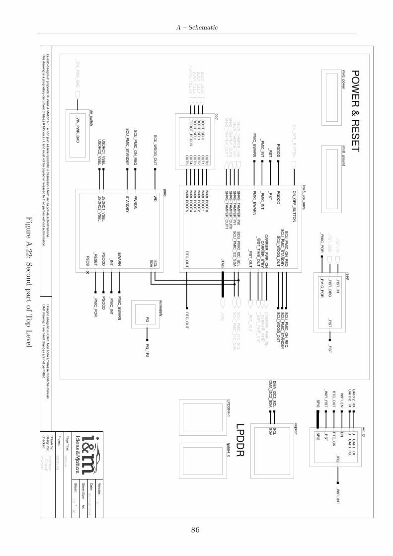
A – Schematic
Dra
wn b
y:
Checked:
Desig
n b
y:
Pro
ject:
Sheet S
ize:
Page T
itle:
Date
:
Vers
ion:
CA
D d
raw
ing. F
ree h
and c
hanges a
re n
ot p
erm
itted.
Dis
egno e
seguito
su C
AD
. Non s
ono a
mm
esse m
odific
he m
anuali.
This
dra
win
g is
a p
roprie
tary
docum
ent o
f Ideas &
Motio
n s
.r.l. and m
ust n
ot b
e c
opie
d o
r rele
ased to
third
partie
s w
ithout a
uth
oriz
atio
n.
Questo
dis
egno e
' pro
prie
ta' d
i Ideas &
Motio
n s
.r.l. e n
on p
uo' e
ssere
ripro
dotto
o tra
sm
esso a
terz
i senza p
revia
auto
rizzazio
ne.
Sheet:
/ A4
Re
vie
we
r
Dra
ftma
n
iMX
8S
OM
L. G
irau
di
22
36
1.0
DD
/M
M/
YY
YY
Mo
du
le
SC
LS
DA SP
I2
BT
_U
AR
T_R
XB
T_U
AR
T_T
X
EN
_R
ST
_IR
QR
TC
_C
K
DM
A_I2
C2_S
CL
DM
A_I2
C2_S
DA
SP
I2
RT
C_O
UT
UA
RT
2_T
XU
AR
T2_R
X
WIF
I_E
N
_W
IFI_
RS
T
_W
IFI_
INT
LP
DD
R4-1
imx8_gro
und
lpddr4
_0
imx8_pow
er
eepro
m
wifi_
bt
WD
I
PW
RO
N
ST
AN
DB
Y
_R
ES
ET
EW
AR
N
_IN
T
US
DH
C1_V
SE
LU
SD
HC
2_V
SE
LP
GO
OD
SC
LS
DA
FS
OB
SC
U_W
DO
G_O
UT
SC
U_P
MIC
_O
N_R
EQ
SC
U_P
MIC
_S
TA
ND
BY
SC
U_P
MIC
_I2
C_S
CL
SC
U_P
MIC
_I2
C_S
DA
_R
ST
PM
IC_E
WA
RN
_P
MIC
_IN
T
ON
_O
FF
_B
UT
TO
N
_W
DT
_T
IME
_O
UT
SN
VS
_T
AM
PE
R_IN
0S
NV
S_T
AM
PE
R_IN
1S
NV
S_T
AM
PE
R_O
UT
0S
NV
S_T
AM
PE
R_O
UT
1
PG
OO
D
_C
AR
RIE
R_S
TB
YC
AR
RIE
R_P
WR
_O
N
JT
AG
RT
C_O
UT
IMX
8_B
OO
T0
IMX
8_B
OO
T1
IMX
8_B
OO
T2
IMX
8_B
OO
T3
IMX
8_B
OO
T4
IMX
8_B
OO
T5
_R
ST
_O
UT
PG
US
DH
C1_V
SE
LU
SD
HC
2_V
SE
L
SC
U_W
DO
G_O
UT
_P
MIC
_P
OR
_R
ST
RT
C_O
UT
pm
ic
SC
U_
PM
IC_
I2C
_S
CL
SC
U_
PM
IC_
I2C
_S
DA
imx8_scu_snvs
auxsupply
ON
_O
FF
_B
UTTO
N
_W
DT_
TIM
E_
OU
T
SN
VS
_TA
MP
ER
_IN
1S
NV
S_
TA
MP
ER
_O
UT0
SN
VS
_TA
MP
ER
_O
UT1
CA
RR
IER
_P
WR
_O
N_
CA
RR
IER
_S
TB
Y
JTA
G
SC
U_P
MIC
_O
N_R
EQ
SC
U_P
MIC
_S
TA
ND
BY
PG
OO
D
_P
MIC
_IN
T
PM
IC_E
WA
RN
PM
IC_E
WA
RN
_P
MIC
_IN
T
PG
OO
D
_R
ST
_IN
_R
ST
_D
BG
_R
ST
_P
MIC
_P
OR
SC
U_W
DO
G_O
UT
_R
ST
_P
MIC
_P
OR
_R
ST_
IN
_V
IN_
PW
R_
BA
D
reset
_R
ST_
DB
G
SC
U_P
MIC
_O
N_R
EQ
SC
U_P
MIC
_S
TA
ND
BY
PO
WE
R &
RE
SE
T
LP
DD
R
PG
_1P
2
_F
OR
CE
_R
EC
OV
_B
OO
T_S
EL2
_B
OO
T_S
EL1
_B
OO
T_S
EL0
OU
T0
OU
T1
OU
T2
OU
T3
OU
T4
OU
T5
boot
_B
OO
T_
SE
L0
_B
OO
T_
SE
L1
_B
OO
T_
SE
L2
_F
OR
CE
_R
EC
OV
_R
ST_
OU
T
_V
IN_P
WR
_B
AD
vin
_sw
itch
SN
VS
_TA
MP
ER
_IN
0
Figu
reA.22:
Secon
dpart
ofTop
Level
86
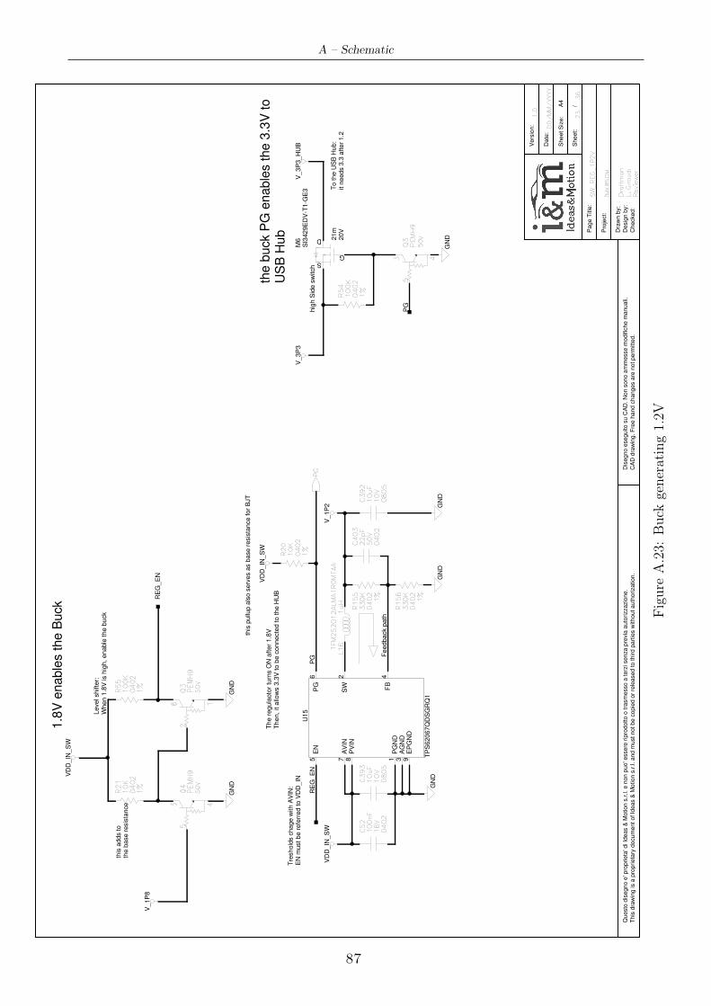
A – Schematic
Dra
wn b
y:
Checked:
Desig
n b
y:
Pro
ject:
Sheet S
ize:
Page T
itle
:
Date
:
Vers
ion:
CA
D d
raw
ing. F
ree h
and c
hanges a
re n
ot perm
itte
d.
Dis
egno e
seguito s
u C
AD
. N
on s
ono a
mm
esse m
odific
he m
anuali.
This
dra
win
g is a
pro
prieta
ry d
ocum
ent of Id
eas &
Motion s
.r.l. and m
ust not be c
opie
d o
r re
leased to third p
art
ies w
ithout auth
orization.
Questo
dis
egno e
' pro
prieta
' di Id
eas &
Motion s
.r.l. e n
on p
uo' e
ssere
rip
rodotto o
tra
sm
esso a
terz
i senza p
revia
auto
rizzazio
ne.
Sheet:
/A4
GN
D
GN
D
RE
G_E
N
PG
AG
ND
EP
GN
D
PG
ND
PV
IN
PG
AV
IN
EN
FB
SW
RE
G_E
N
GN
DG
ND
GN
D
PG F
eedback p
ath
Level shifte
r:W
hen 1
.8V
is h
igh, enable
the b
uck
hig
h S
ide s
witch
The r
egula
oto
r tu
rns O
N a
fter
1.8
VT
hen, it a
llow
s 3
.3V
to b
e c
onnecte
d to the H
UB
this
pullu
p a
lso s
erv
es a
s b
ase r
esis
tance for
BJT
To the U
SB
Hub:
it n
eeds 3
.3 a
fter
1.2
Tre
shold
s c
hage w
ith A
VIN
:E
N m
ust be r
efe
rred to V
DD
_IN
Re
vie
we
r
Dra
ftm
an
iMX
8S
OM
L.
Gir
au
di
23
36
1.0
DD
/M
M/
YY
YY
SW
_R
EG
_1
P2
V
VD
D_IN
_S
W
04
02
R5
4
1%
10
0K
TP
S62067Q
DS
GR
Q1
U15
2 4
5 7
6
8 1 93
VD
D_IN
_S
W
L1
6TF
M2
52
01
2A
LM
A1
R0
MTA
A1
uH
C4
03
04
02
22
pF
50
V
V_1P
2
PG
V_1P
8
V_3P
3V
_3P
3_H
UB
M6
S
D
G
SI3
429E
DV
-T1-G
E3
21m
20V
R2
0
04
02
10
K
1%
R1
55
04
02
33
0K
1%
1%
33
0K
04
02
R1
56
C5
2
04
02
10
0n
F1
6V
1.8
V e
nable
s the B
uck
the b
uck P
G e
nable
s the 3
.3V
to
US
B H
ub
43
5Q
4P
EM
H9
50
V
43
5Q
3P
EM
H9
50
V
C3
92
08
05
10
uF
10
V1
0V
10
uF
08
05
C3
93
VD
D_IN
_S
W
GN
D
04
02
R5
5
1%
10
0K
16
2Q
3P
EM
H9
50
V
R2
1
04
02
10
K
1%
this
adds to
the b
ase r
esis
tance
Figure
A.23:
Buck
generating1.2V
87
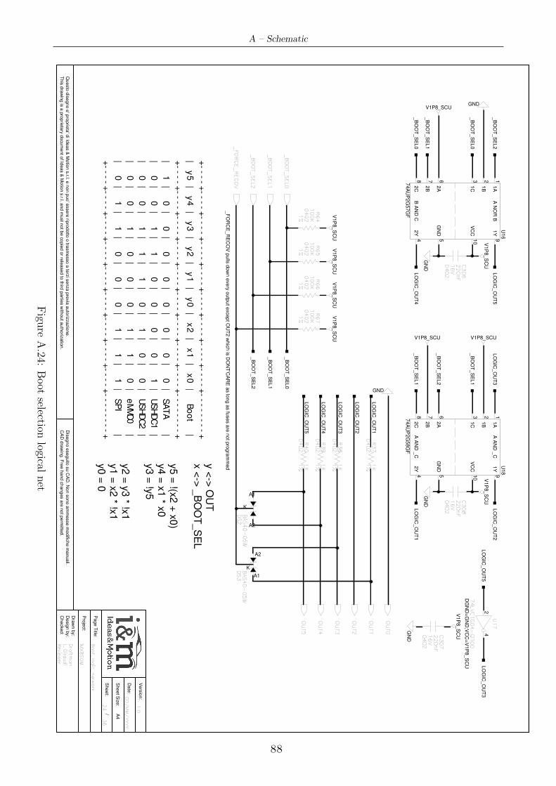
A – Schematic
GN
D
1A
1B
1C
1Y
2A
2B
2C
2Y
GN
D
VC
C
1A
1B
1C
1Y
2A
2B
2C
2Y
GN
D
VC
C
A N
OR
B
B A
ND
C
A A
ND
_C
A A
ND
_C
y <
-> O
UT
x <
-> _
BO
OT
_S
EL
y5 =
!(x2 +
x0)
y4 =
x1 * x
0y3 =
!y5
y2 =
y3 * !x
1y1 =
x2 * !x
1y0 =
0
+-
--
-+
--
--
+-
--
-+
--
--
+-
--
-+
--
--
+-
--
-+
--
--
+-
--
-+
--
--
--
--
+
|
y5
|
y
4
|
y3
|
y
2
|
y1
|
y
0
|
x2
|
x
1
|
x0
|
Bo
ot
|
+-
--
-+
--
--
+-
--
-+
--
--
+-
--
-+
--
--
+-
--
-+
--
--
+-
--
-+
--
--
--
--
+
|
1
|
0
|
0
|
0
|
0
|
0
|
0
|
0
|
0
|
S
AT
A
|
|
0
|
0
|
1
|
1
|
0
|
0
|
0
|
0
|
1
|
U
SH
DC
1
|
|
0
|
0
|
1
|
1
|
1
|
0
|
1
|
0
|
0
|
U
SH
DC
2
|
|
0
|
0
|
1
|
0
|
0
|
0
|
1
|
1
|
0
|
e
MM
C0
|
|
0
|
1
|
1
|
0
|
0
|
0
|
1
|
1
|
1
|
S
PI
|
+-
--
-+
--
--
+-
--
-+
--
--
+-
--
-+
--
--
+-
--
-+
--
--
+-
--
-+
--
--
--
--
+
_F
OR
CE
_R
EC
OV
pulls
dow
n e
very
outp
ut e
xcept O
UT
2 w
hic
h is
DO
NT
'CA
RE
as lo
ng a
s fu
ses a
re n
ot p
rogra
mm
ed
_B
OO
T_S
EL0
_B
OO
T_S
EL2
_B
OO
T_S
EL1
LO
GIC
_O
UT
4
_B
OO
T_S
EL0
_B
OO
T_S
EL2
_B
OO
T_S
EL0
_B
OO
T_S
EL1
LO
GIC
_O
UT
3
_B
OO
T_S
EL1
_B
OO
T_S
EL1
_B
OO
T_S
EL2
LO
GIC
_O
UT
1
LO
GIC
_O
UT
1
LO
GIC
_O
UT
3
LO
GIC
_O
UT
4
LO
GIC
_O
UT
5
Dra
wn b
y:
Checked:
Desig
n b
y:
Pro
ject:
Sheet S
ize:
Page T
itle:
Date
:
Vers
ion:
CA
D d
raw
ing. F
ree h
and c
hanges a
re n
ot p
erm
itted.
Dis
egno e
seguito
su C
AD
. Non s
ono a
mm
esse m
odific
he m
anuali.
This
dra
win
g is
a p
roprie
tary
docum
ent o
f Ideas &
Motio
n s
.r.l. and m
ust n
ot b
e c
opie
d o
r rele
ased to
third
partie
s w
ithout a
uth
oriz
atio
n.
Questo
dis
egno e
' pro
prie
ta' d
i Ideas &
Motio
n s
.r.l. e n
on p
uo' e
ssere
ripro
dotto
o tra
sm
esso a
terz
i senza p
revia
auto
rizzazio
ne.
Sheet:
/ A4
LO
GIC
_O
UT
2
GN
D
LO
GIC
_O
UT
3LO
GIC
_O
UT
5
LO
GIC
_O
UT
5LO
GIC
_O
UT
2
GN
D
GND
GND
K
A1
A2
K
A1
A2
V1P
8_S
CU
V1P8_SCU V1P8_SCU
V1P8_SCU
V1P
8_S
CU
_F
OR
CE
_R
EC
OV
_B
OO
T_
SE
L1
_B
OO
T_
SE
L2
_B
OO
T_
SE
L0
DD
/M
M/
YY
YY
Bo
ot_
log
ic_
ne
two
rk
Re
vie
we
r
L. G
irau
di
iMX
8S
OM
Dra
ftma
n
24
36
1.0
OU
T1
OU
T5
OU
T2
OU
T3
OU
T4
OU
T0
V1P
8_S
CU
V1P
8_S
CU
V1P
8_S
CU
V1P
8_S
CU
V1P
8_S
CU
16
V2
20
nF
04
02
C3
06
DG
ND
=G
ND
;VC
C=
V1P
8_S
CU
U1
7
74
LV
C1
G0
4-
Q1
00
24
DS
2B
AS
40
-0
5W
DS
3B
AS
40
-0
5W
16
V2
20
nF
04
02
C3
07
04
02
1%
10
0K
R6
4
04
02
1%
10
0K
R6
5
1%
1K
04
02
R4
00
40
21
%
10
0K
R6
6
04
02
1%
10
0K
R6
7
74A
UP
2G
57G
F
U16
10
548 7 6
9
3 2 1
74A
UP
2G
58G
F
U18
10
548 7 6
9
3 2 1
1%
1K
04
02
R3
7
16
V2
20
nF
04
02
C3
08
1%
1K
04
02
R3
8
R3
90
40
21
K1
%
Figu
reA.24:
Boot
selectionlogical
net
88
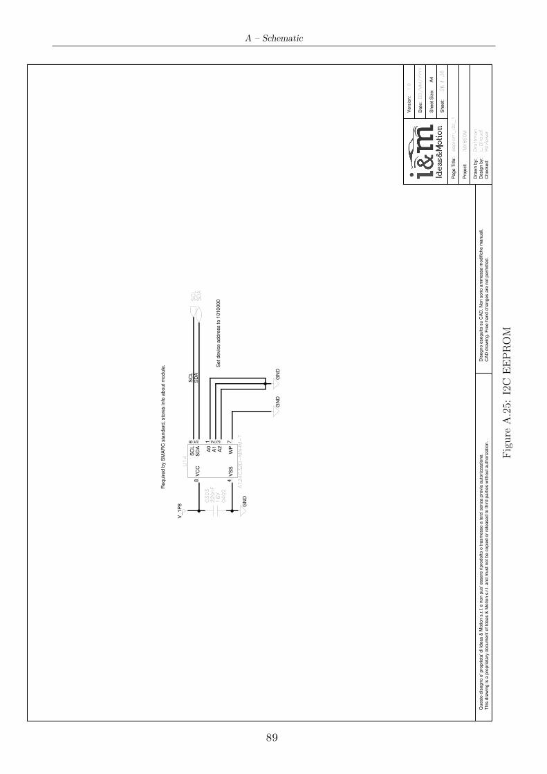
A – Schematic
GN
D
GN
D
Set devic
e a
ddre
ss to 1
010000
Required b
y S
MA
RC
sta
ndard
, sto
res info
about m
odule
.
V_1P
8
22
0n
F1
6V
C3
03
04
02
SD
AS
CL
Dra
wn b
y:
Checked:
Desig
n b
y:
Pro
ject:
Sheet S
ize:
Page T
itle
:
Date
:
Vers
ion:
CA
D d
raw
ing. F
ree h
and c
hanges a
re n
ot perm
itte
d.
Dis
egno e
seguito s
u C
AD
. N
on s
ono a
mm
esse m
odific
he m
anuali.
This
dra
win
g is a
pro
prieta
ry d
ocum
ent of Id
eas &
Motion s
.r.l. and m
ust not be c
opie
d o
r re
leased to third p
art
ies w
ithout auth
orization.
Questo
dis
egno e
' pro
prieta
' di Id
eas &
Motion s
.r.l. e n
on p
uo' e
ssere
rip
rodotto o
tra
sm
esso a
terz
i senza p
revia
auto
rizzazio
ne.
Sheet:
/A4
Re
vie
we
r
L.
Gir
au
di
iMX
8S
OM
Dra
ftm
an
26
36
1.0
DD
/M
M/
YY
YY
ee
pro
m_
i2c
_1
GN
D
A0
A1
A2
VS
S
VC
C
WP
SC
LS
DA
U1
4
56 7
8 4
321
AT2
4C
32
D-
MA
HM
-T
SC
LS
DA
Figure
A.25:
I2C
EEPROM
89
A – Schematic
VS
S_M
AIN
_A
G5
VS
S_M
AIN
_A
R5
VS
S_M
AIN
_A
R49
VS
S_M
AIN
_A
R35
VS
S_M
AIN
_A
R31
VS
S_M
AIN
_A
R27
VS
S_M
AIN
_A
R23
VS
S_M
AIN
_A
R19
VS
S_M
AIN
_A
R11
VS
S_M
AIN
_A
P34
VS
S_M
AIN
_A
P30
VS
S_M
AIN
_A
P26
VS
S_M
AIN
_A
P22
VS
S_M
AIN
_A
P18
VS
S_M
AIN
_A
P12
VS
S_M
AIN
_A
N7
VS
S_M
AIN
_A
N53
VS
S_M
AIN
_A
N51
VS
S_M
AIN
_A
N5
VS
S_M
AIN
_A
N49
VS
S_M
AIN
_A
N47
VS
S_M
AIN
_A
N43
VS
S_M
AIN
_A
N41
VS
S_M
AIN
_A
N33
VS
S_M
AIN
_A
N3
VS
S_M
AIN
_A
N29
VS
S_M
AIN
_A
N25
VS
S_M
AIN
_A
N21
VS
S_M
AIN
_A
N17
VS
S_M
AIN
_A
N13
VS
S_M
AIN
_A
N1
VS
S_M
AIN
_A
M8
VS
S_M
AIN
_A
M46
VS
S_M
AIN
_A
M42
VS
S_M
AIN
_A
M36
VS
S_M
AIN
_A
M32
VS
S_M
AIN
_A
M28
VS
S_M
AIN
_A
M24
VS
S_M
AIN
_A
M20
VS
S_M
AIN
_A
M12
VS
S_M
AIN
_A
L41
VS
S_M
AIN
_A
L35
VS
S_M
AIN
_A
L31
VS
S_M
AIN
_A
L27
VS
S_M
AIN
_A
L23
VS
S_M
AIN
_A
L19
VS
S_M
AIN
_A
L13
VS
S_M
AIN
_A
K8
VS
S_M
AIN
_A
K6
VS
S_M
AIN
_A
K52
VS
S_M
AIN
_A
K50
VS
S_M
AIN
_A
K48
VS
S_M
AIN
_A
K46
VS
S_M
AIN
_A
K44
VS
S_M
AIN
_A
K4
VS
S_M
AIN
_A
K38
VS
S_M
AIN
_A
K34
VS
S_M
AIN
_A
K30
VS
S_M
AIN
_A
K26
VS
S_M
AIN
_A
K22
VS
S_M
AIN
_A
K2
VS
S_M
AIN
_A
K18
VS
S_M
AIN
_A
K12
VS
S_M
AIN
_A
K10
VS
S_M
AIN
_A
J41
VS
S_M
AIN
_A
J37
VS
S_M
AIN
_A
J33
VS
S_M
AIN
_A
J29
VS
S_M
AIN
_A
J25
VS
S_M
AIN
_A
J21
VS
S_M
AIN
_A
J17
VS
S_M
AIN
_A
J13
VS
S_M
AIN
_A
H42
VS
S_M
AIN
_A
H36
VS
S_M
AIN
_A
H32
VS
S_M
AIN
_A
H28
VS
S_M
AIN
_A
H24
VS
S_M
AIN
_A
H20
VS
S_M
AIN
_A
H12
VS
S_M
AIN
_A
G9
VS
S_M
AIN
_A
G7
VS
S_M
AIN
_A
G53
VS
S_M
AIN
_A
G51
VS
S_M
AIN
_A
G49
VS
S_M
AIN
_A
T12
VS
S_M
AIN
_A
G47
VS
S_M
AIN
_A
G45
VS
S_M
AIN
_A
G43
VS
S_M
AIN
_A
G41
VS
S_M
AIN
_A
G35
VS
S_M
AIN
_A
G31
VS
S_M
AIN
_A
G3
VS
S_M
AIN
_A
G27
VS
S_M
AIN
_A
G23
VS
S_M
AIN
_A
G19
VS
S_M
AIN
_A
G13
VS
S_M
AIN
_A
G11
VS
S_M
AIN
_A
G1
VS
S_M
AIN
_A
F42
VS
S_M
AIN
_A
F34
VS
S_M
AIN
_A
F30
VS
S_M
AIN
_A
F26
VS
S_M
AIN
_A
F22
VS
S_M
AIN
_A
F18
VS
S_M
AIN
_A
F12
VS
S_M
AIN
_A
E41
VS
S_M
AIN
_A
E37
VS
S_M
AIN
_A
E33
VS
S_M
AIN
_A
E29
VS
S_M
AIN
_A
E25
VS
S_M
AIN
_A
E21
VS
S_M
AIN
_A
E17
VS
S_M
AIN
_A
E13
VS
S_M
AIN
_A
D8
VS
S_M
AIN
_A
D6
VS
S_M
AIN
_A
D52
VS
S_M
AIN
_A
D50
VS
S_M
AIN
_A
D48
VS
S_M
AIN
_A
D46
VS
S_M
AIN
_A
D44
VS
S_M
AIN
_A
D42
VS
S_M
AIN
_A
D4
VS
S_M
AIN
_A
D36
VS
S_M
AIN
_A
D32
VS
S_M
AIN
_A
D28
VS
S_M
AIN
_A
D24
VS
S_M
AIN
_A
D20
VS
S_M
AIN
_A
D2
VS
S_M
AIN
_A
D12
VS
S_M
AIN
_A
D10
VS
S_M
AIN
_A
C41
VS
S_M
AIN
_A
C35
VS
S_M
AIN
_A
C31
VS
S_M
AIN
_A
C27
VS
S_M
AIN
_A
C23
VS
S_M
AIN
_A
C19
VS
S_M
AIN
_A
C13
VS
S_M
AIN
_A
B42
VS
S_M
AIN
_A
B34
VS
S_M
AIN
_A
B30
VS
S_M
AIN
_A
B26
VS
S_M
AIN
_A
B22
VS
S_M
AIN
_A
B18
VS
S_M
AIN
_A
B12
VS
S_M
AIN
_A
A9
VS
S_M
AIN
_A
A7
VS
S_M
AIN
_A
A53
VS
S_M
AIN
_A
A51
VS
S_M
AIN
_A
A5
VS
S_M
AIN
_A
A49
VS
S_M
AIN
_A
A47
VS
S_M
AIN
_A
A45
VS
S_M
AIN
_A
A43
VS
S_M
AIN
_A
A41
VS
S_M
AIN
_A
A37
VS
S_M
AIN
_A
A33
VS
S_M
AIN
_A
A3
VS
S_M
AIN
_A
A29
VS
S_M
AIN
_A
A25
VS
S_M
AIN
_A
A21
VS
S_M
AIN
_A
A17
VS
S_M
AIN
_A
A13
VS
S_M
AIN
_A
A11
VS
S_M
AIN
_A
A1
VS
S_M
AIN
_A
51
VS
S_M
AIN
_A
31
VS
S_M
AIN
_A
3V
SS
_M
AIN
_A
23 U
1
A23
A3
A31
A51
AA
1A
A11
AA
13
AA
17
AA
21
AA
25
AA
29
AA
3A
A33
AA
37
AA
41
AA
43
AA
45
AA
47
AA
49
AA
5A
A51
AA
53
AA
7A
A9
AB
12
AB
18
AB
22
AB
26
AB
30
AB
34
AB
42
AC
13
AC
19
AC
23
AC
27
AC
31
AC
35
AC
41
AD
10
AD
12
AD
2A
D20
AD
24
AD
28
AD
32
AD
36
AD
4A
D42
AD
44
AD
46
AD
48
AD
50
AD
52
AD
6A
D8
AE
13
AE
17
AE
21
AE
25
AE
29
AE
33
AE
37
AE
41
AF
12
AF
18
AF
22
AF
26
AF
30
AF
34
AF
42
AG
1A
G11
AG
13
AG
19
AG
23
AG
27
AG
3A
G31
AG
35
AG
41
AG
43
AG
45
AG
47
AT
12
AG
49
AG
51
AG
53
AG
7A
G9
AH
12
AH
20
AH
24
AH
28
AH
32
AH
36
AH
42
AJ13
AJ17
AJ21
AJ25
AJ29
AJ33
AJ37
AJ41
AK
10
AK
12
AK
18
AK
2A
K22
AK
26
AK
30
AK
34
AK
38
AK
4A
K44
AK
46
AK
48
AK
50
AK
52
AK
6A
K8
AL13
AL19
AL23
AL27
AL31
AL35
AL41
AM
12
AM
20
AM
24
AM
28
AM
32
AM
36
AM
42
AM
46
AM
8A
N1
AN
13
AN
17
AN
21
AN
25
AN
29
AN
3A
N33
AN
41
AN
43
AN
47
AN
49
AN
5A
N51
AN
53
AN
7A
P12
AP
18
AP
22
AP
26
AP
30
AP
34
AR
11
AR
19
AR
23
AR
27
AR
31
AR
35
AR
49
AR
5A
G5
PIM
X8M
6A
VU
DD
1A
VS
S_M
AIN
_B
C35
VS
S_M
AIN
_C
33
VS
S_M
AIN
_C
31
VS
S_M
AIN
_C
29
VS
S_M
AIN
_C
23
VS
S_M
AIN
_C
21
VS
S_M
AIN
_C
19
VS
S_M
AIN
_C
15
VS
S_M
AIN
_C
11
VS
S_M
AIN
_C
1V
SS
_M
AIN
_B
N3
VS
S_M
AIN
_B
N21
VS
S_M
AIN
_B
M46
VS
S_M
AIN
_B
M10
VS
S_M
AIN
_B
L53
VS
S_M
AIN
_B
L21
VS
S_M
AIN
_B
L1
VS
S_M
AIN
_B
K8
VS
S_M
AIN
_B
K6
VS
S_M
AIN
_B
K46
VS
S_M
AIN
_B
K22
VS
S_M
AIN
_B
K20
VS
S_M
AIN
_B
K18
VS
S_M
AIN
_B
K16
VS
S_M
AIN
_B
K14
VS
S_M
AIN
_B
K12
VS
S_M
AIN
_B
K10
VS
S_M
AIN
_B
J51
VS
S_M
AIN
_B
J5
VS
S_M
AIN
_B
J49
VS
S_M
AIN
_B
J47
VS
S_M
AIN
_B
J45
VS
S_M
AIN
_B
J43
VS
S_M
AIN
_B
J41
VS
S_M
AIN
_B
J39
VS
S_M
AIN
_B
J37
VS
S_M
AIN
_B
J35
VS
S_M
AIN
_B
J33
VS
S_M
AIN
_B
J31
VS
S_M
AIN
_B
J3
VS
S_M
AIN
_B
J29
VS
S_M
AIN
_B
J27
VS
S_M
AIN
_B
J25
VS
S_M
AIN
_B
H4
VS
S_M
AIN
_B
H22
VS
S_M
AIN
_B
G7
VS
S_M
AIN
_B
G47
VS
S_M
AIN
_B
G23
VS
S_M
AIN
_B
G21
VS
S_M
AIN
_B
G19
VS
S_M
AIN
_B
G17
VS
S_M
AIN
_B
G15
VS
S_M
AIN
_B
G13
VS
S_M
AIN
_B
G11
VS
S_M
AIN
_B
F52
VS
S_M
AIN
_B
F44
VS
S_M
AIN
_B
F42
VS
S_M
AIN
_B
F40
VS
S_M
AIN
_B
F4
VS
S_M
AIN
_B
F38
VS
S_M
AIN
_B
F36
VS
S_M
AIN
_B
F34
VS
S_M
AIN
_B
F32
VS
S_M
AIN
_B
F30
VS
S_M
AIN
_B
F28
VS
S_M
AIN
_B
F26
VS
S_M
AIN
_B
E9
VS
S_M
AIN
_B
E7
VS
S_M
AIN
_B
E45
VS
S_M
AIN
_B
E3
VS
S_M
AIN
_B
D50
VS
S_M
AIN
_B
D48
VS
S_M
AIN
_B
D26
VS
S_M
AIN
_B
D24
VS
S_M
AIN
_B
D22
VS
S_M
AIN
_B
D20
VS
S_M
AIN
_B
D18
VS
S_M
AIN
_B
D16
VS
S_M
AIN
_B
D14
VS
S_M
AIN
_B
C43
VS
S_M
AIN
_B
C41
VS
S_M
AIN
_B
C39
VS
S_M
AIN
_B
C37
VS
S_M
AIN
_B
C31
VS
S_M
AIN
_B
C33
VS
S_M
AIN
_C
41
VS
S_M
AIN
_B
C29
VS
S_M
AIN
_B
C27
VS
S_M
AIN
_B
C25
VS
S_M
AIN
_B
C23
VS
S_M
AIN
_B
C21
VS
S_M
AIN
_B
C19
VS
S_M
AIN
_B
C17
VS
S_M
AIN
_B
C15
VS
S_M
AIN
_B
C13
VS
S_M
AIN
_B
C11
VS
S_M
AIN
_B
B6
VS
S_M
AIN
_B
B52
VS
S_M
AIN
_B
B48
VS
S_M
AIN
_B
B40
VS
S_M
AIN
_B
B38
VS
S_M
AIN
_B
B36
VS
S_M
AIN
_B
B34
VS
S_M
AIN
_B
B32
VS
S_M
AIN
_B
B30
VS
S_M
AIN
_B
B28
VS
S_M
AIN
_B
B26
VS
S_M
AIN
_B
B24
VS
S_M
AIN
_B
B22
VS
S_M
AIN
_B
B20
VS
S_M
AIN
_B
B2
VS
S_M
AIN
_B
B18
VS
S_M
AIN
_B
B16
VS
S_M
AIN
_B
B14
VS
S_M
AIN
_B
B10
VS
S_M
AIN
_B
A45
VS
S_M
AIN
_B
A41
VS
S_M
AIN
_B
A39
VS
S_M
AIN
_B
A37
VS
S_M
AIN
_B
A35
VS
S_M
AIN
_B
A33
VS
S_M
AIN
_B
A31
VS
S_M
AIN
_B
A29
VS
S_M
AIN
_B
A27
VS
S_M
AIN
_B
A25
VS
S_M
AIN
_B
A23
VS
S_M
AIN
_B
A21
VS
S_M
AIN
_B
A19
VS
S_M
AIN
_B
A17
VS
S_M
AIN
_B
A15
VS
S_M
AIN
_B
A13
VS
S_M
AIN
_B
6V
SS
_M
AIN
_B
46
VS
S_M
AIN
_B
36
VS
S_M
AIN
_B
28
VS
S_M
AIN
_B
18
VS
S_M
AIN
_B
14
VS
S_M
AIN
_B
12
VS
S_M
AIN
_A
W7
VS
S_M
AIN
_A
W51
VS
S_M
AIN
_A
W47
VS
S_M
AIN
_A
W43
VS
S_M
AIN
_A
W37
VS
S_M
AIN
_A
W3
VS
S_M
AIN
_A
W23
VS
S_M
AIN
_A
W19
VS
S_M
AIN
_A
W11
VS
S_M
AIN
_A
V42
VS
S_M
AIN
_A
V38
VS
S_M
AIN
_A
V12
VS
S_M
AIN
_A
U37
VS
S_M
AIN
_A
U33
VS
S_M
AIN
_A
U31
VS
S_M
AIN
_A
U25
VS
S_M
AIN
_A
U17
VS
S_M
AIN
_A
T8
VS
S_M
AIN
_A
T6
VS
S_M
AIN
_A
T52
VS
S_M
AIN
_A
T50
VS
S_M
AIN
_A
T46
VS
S_M
AIN
_A
T42
VS
S_M
AIN
_A
T4
VS
S_M
AIN
_A
T36
VS
S_M
AIN
_A
T32
VS
S_M
AIN
_A
T28
VS
S_M
AIN
_A
T24
VS
S_M
AIN
_A
T20
VS
S_M
AIN
_A
T2
VS
S_M
AIN
_A
T16 U1
AT
16
AT
2A
T20
AT
24
AT
28
AT
32
AT
36
AT
4A
T42
AT
46
AT
50
AT
52
AT
6A
T8
AU
17
AU
25
AU
31
AU
33
AU
37
AV
12
AV
38
AV
42
AW
11
AW
19
AW
23
AW
3A
W37
AW
43
AW
47
AW
51
AW
7B
12
B14
B18
B28
B36
B46
B6
BA
13
BA
15
BA
17
BA
19
BA
21
BA
23
BA
25
BA
27
BA
29
BA
31
BA
33
BA
35
BA
37
BA
39
BA
41
BA
45
BB
10
BB
14
BB
16
BB
18
BB
2B
B20
BB
22
BB
24
BB
26
BB
28
BB
30
BB
32
BB
34
BB
36
BB
38
BB
40
BB
48
BB
52
BB
6B
C11
BC
13
BC
15
BC
17
BC
19
BC
21
BC
23
BC
25
BC
27
BC
29
C41
PIM
X8M
6A
VU
DD
1A
VS
S_M
AIN
_L33
VS
S_M
AIN
_Y
36
VS
S_M
AIN
_Y
32
VS
S_M
AIN
_Y
28
VS
S_M
AIN
_Y
24
VS
S_M
AIN
_Y
20
VS
S_M
AIN
_Y
12
VS
S_M
AIN
_W
35
VS
S_M
AIN
_W
31
VS
S_M
AIN
_W
27
VS
S_M
AIN
_W
23
VS
S_M
AIN
_W
19
VS
S_M
AIN
_V
8V
SS
_M
AIN
_V
6V
SS
_M
AIN
_V
52
VS
S_M
AIN
_V
50
VS
S_M
AIN
_V
48
VS
S_M
AIN
_V
46
VS
S_M
AIN
_V
44
VS
S_M
AIN
_V
42
VS
S_M
AIN
_V
4V
SS
_M
AIN
_V
34
VS
S_M
AIN
_V
30
VS
S_M
AIN
_V
22
VS
S_M
AIN
_V
2V
SS
_M
AIN
_V
18
VS
S_M
AIN
_V
12
VS
S_M
AIN
_V
10
VS
S_M
AIN
_U
37
VS
S_M
AIN
_U
33
VS
S_M
AIN
_U
21
VS
S_M
AIN
_U
17
VS
S_M
AIN
_T
42
VS
S_M
AIN
_T
36
VS
S_M
AIN
_T
32
VS
S_M
AIN
_T
28
VS
S_M
AIN
_T
24
VS
S_M
AIN
_T
20
VS
S_M
AIN
_T
16
VS
S_M
AIN
_T
12
VS
S_M
AIN
_R
9V
SS
_M
AIN
_R
7V
SS
_M
AIN
_R
53
VS
S_M
AIN
_R
51
VS
S_M
AIN
_R
5V
SS
_M
AIN
_R
49
VS
S_M
AIN
_R
47
VS
S_M
AIN
_R
45
VS
S_M
AIN
_R
43
VS
S_M
AIN
_R
39
VS
S_M
AIN
_R
37
VS
S_M
AIN
_R
35
VS
S_M
AIN
_R
33
VS
S_M
AIN
_R
31
VS
S_M
AIN
_R
3V
SS
_M
AIN
_R
29
VS
S_M
AIN
_R
27
VS
S_M
AIN
_R
25
VS
S_M
AIN
_R
23
VS
S_M
AIN
_R
21
VS
S_M
AIN
_R
19
VS
S_M
AIN
_R
17
VS
S_M
AIN
_R
15
VS
S_M
AIN
_R
11
VS
S_M
AIN
_R
1V
SS
_M
AIN
_P
42
VS
S_M
AIN
_P
12
VS
S_M
AIN
_N
41
VS
S_M
AIN
_N
13
VS
S_M
AIN
_M
8V
SS
_M
AIN
_M
6V
SS
_M
AIN
_M
52
VS
S_M
AIN
_M
50
VS
S_M
AIN
_M
48
VS
S_M
AIN
_M
46
VS
S_M
AIN
_M
44
VS
S_M
AIN
_M
4V
SS
_M
AIN
_M
2V
SS
_M
AIN
_M
10
VS
S_M
AIN
_L43
VS
S_M
AIN
_L41
VS
S_M
AIN
_L39
VS
S_M
AIN
_L37
VS
S_M
AIN
_L29
VS
S_M
AIN
_L31
VS
S_M
AIN
_Y
42
VS
S_M
AIN
_L35
VS
S_M
AIN
_L27
VS
S_M
AIN
_L25
VS
S_M
AIN
_L23
VS
S_M
AIN
_L21
VS
S_M
AIN
_L19
VS
S_M
AIN
_L17
VS
S_M
AIN
_L15
VS
S_M
AIN
_L13
VS
S_M
AIN
_L11
VS
S_M
AIN
_K
8V
SS
_M
AIN
_K
46
VS
S_M
AIN
_K
42
VS
S_M
AIN
_K
40
VS
S_M
AIN
_K
38
VS
S_M
AIN
_K
36
VS
S_M
AIN
_K
34
VS
S_M
AIN
_K
32
VS
S_M
AIN
_K
30
VS
S_M
AIN
_K
28
VS
S_M
AIN
_K
26
VS
S_M
AIN
_K
24
VS
S_M
AIN
_K
22
VS
S_M
AIN
_K
20
VS
S_M
AIN
_K
18
VS
S_M
AIN
_K
16
VS
S_M
AIN
_K
14
VS
S_M
AIN
_K
12
VS
S_M
AIN
_J7
VS
S_M
AIN
_J53
VS
S_M
AIN
_J51
VS
S_M
AIN
_J5
VS
S_M
AIN
_J49
VS
S_M
AIN
_J47
VS
S_M
AIN
_J41
VS
S_M
AIN
_J37
VS
S_M
AIN
_J35
VS
S_M
AIN
_J31
VS
S_M
AIN
_J3
VS
S_M
AIN
_J29
VS
S_M
AIN
_J25
VS
S_M
AIN
_J23
VS
S_M
AIN
_J21
VS
S_M
AIN
_J19
VS
S_M
AIN
_J17
VS
S_M
AIN
_J15
VS
S_M
AIN
_J13
VS
S_M
AIN
_J1
VS
S_M
AIN
_G
9V
SS
_M
AIN
_G
5V
SS
_M
AIN
_G
49
VS
S_M
AIN
_G
39
VS
S_M
AIN
_G
33
VS
S_M
AIN
_G
27
VS
S_M
AIN
_G
23
VS
S_M
AIN
_G
21
VS
S_M
AIN
_G
15
VS
S_M
AIN
_F
52
VS
S_M
AIN
_F
50
VS
S_M
AIN
_F
44
VS
S_M
AIN
_F
4V
SS
_M
AIN
_F
36
VS
S_M
AIN
_F
32
VS
S_M
AIN
_F
24
VS
S_M
AIN
_F
2V
SS
_M
AIN
_F
12
VS
S_M
AIN
_E
9V
SS
_M
AIN
_E
47
VS
S_M
AIN
_E
21
VS
S_M
AIN
_E
19
VS
S_M
AIN
_D
6V
SS
_M
AIN
_D
40
VS
S_M
AIN
_D
38
VS
S_M
AIN
_D
36
VS
S_M
AIN
_D
34
VS
S_M
AIN
_D
28
VS
S_M
AIN
_D
26
VS
S_M
AIN
_D
24
VS
S_M
AIN
_D
18
VS
S_M
AIN
_D
16
VS
S_M
AIN
_C
9V
SS
_M
AIN
_C
53
VS
S_M
AIN
_C
49
VS
S_M
AIN
_C
43 U
1
C43
C49
C53
C9
D16
D18
D24
D26
D28
D34
D36
D38
D40
D6
E19
E21
E47
E9
F12
F2
F24
F32
F36
F4
F44
F50
F52
G15
G21
G23
G27
G33
G39
G49
G5
G9
J1
J13
J15
J17
J19
J21
J23
J25
J29
J3
J31
J35
J37
J41
J47
J49
J5
J51
J53
J7
K12
K14
K16
K18
K20
K22
K24
K26
K28
K30
K32
K34
K36
K38
K40
K42
K46
K8
L11
L13
L15
L17
L19
L21
L23
L25
L27
L35
Y42
L31
L29
L37
L39
L41
L43
M10
M2
M4
M44
M46
M48
M50
M52
M6
M8
N13
N41
P12
P42
R1
R11
R15
R17
R19
R21
R23
R25
R27
R29
R3
R31
R33
R35
R37
R39
R43
R45
R47
R49
R5
R51
R53
R7
R9
T12
T16
T20
T24
T28
T32
T36
T42
U17
U21
U33
U37
V10
V12
V18
V2
V22
V30
V34
V4
V42
V44
V46
V48
V50
V52
V6
V8
W19
W23
W27
W31
W35
Y12
Y20
Y24
Y28
Y32
Y36
L33
PIM
X8M
6A
VU
DD
1A
Dra
wn b
y:
Checked:
Desig
n b
y:
Pro
ject:
Sheet S
ize:
Page T
itle:
Sheet:
Date
:
Vers
ion:
CA
D d
raw
ing. F
ree h
and c
hanges a
re n
ot p
erm
itted.
Dis
egno e
seguito
su C
AD
. Non s
ono a
mm
esse m
odific
he m
anuali.
This
dra
win
g is
a p
roprie
tary
docum
ent o
f Ideas &
Motio
n s
.r.l. and m
ust n
ot b
e c
opie
d o
r rele
ased to
third
partie
s w
ithout a
uth
oriz
atio
n.
Questo
dis
egno e
' pro
prie
ta' d
i Ideas &
Motio
n s
.r.l. e n
on p
uo' e
ssere
ripro
dotto
o tra
sm
esso a
terz
i senza p
revia
auto
rizzazio
ne.
/ A3
12
34
56
78
ABCDEF
Re
vie
we
r
Dra
ftma
n
iMX
8S
OM
L. G
irau
di
27
36
1.0
DD
/M
M/
YY
YY
imx
8_
gro
un
d
GN
DG
ND
GN
DG
ND
GN
DG
ND
Figu
reA.26:
Grou
ndblock
iMX8
90
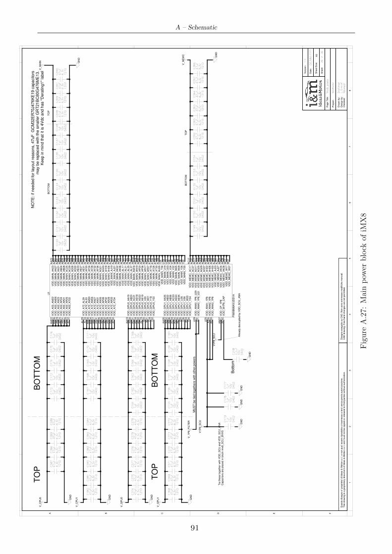
A – Schematic
Dra
wn b
y:
Checked:
Desig
n b
y:
Pro
ject:
Sheet S
ize:
Page T
itle
:
Sheet:
Date
:
Vers
ion:
CA
D d
raw
ing. F
ree h
and c
hanges a
re n
ot perm
itte
d.
Dis
egno e
seguito s
u C
AD
. N
on s
ono a
mm
esse m
odific
he m
anuali.
This
dra
win
g is a
pro
prieta
ry d
ocum
ent of Id
eas &
Motion s
.r.l. and m
ust not be c
opie
d o
r re
leased to third p
art
ies w
ithout auth
orization.
Questo
dis
egno e
' pro
prieta
' di Id
eas &
Motion s
.r.l. e n
on p
uo' e
ssere
rip
rodotto o
tra
sm
esso a
terz
i senza p
revia
auto
rizzazio
ne.
/A3
12
34
56
78
A B C D E F
Re
vie
we
r
Dra
ftm
an
iMX
8S
OM
L.
Gir
au
di
28
36
1.0
DD
/M
M/
YY
YY
imx
8_
po
we
r
VD
D_A
53_A
M22
VD
D_A
53_A
M26
VD
D_A
53_A
N23
VD
D_A
53_A
P24
VD
D_A
53_A
R21
VD
D_A
53_A
R25
VD
D_A
53_A
T22
VD
D_A
72_A
L29
VD
D_A
72_A
L33
VD
D_A
72_A
M30
VD
D_A
72_A
M34
VD
D_A
72_A
N27
VD
D_A
72_A
N31
VD
D_A
72_A
N35
VD
D_A
72_A
P28
VD
D_A
72_A
P32
VD
D_A
72_A
R29
VD
D_A
72_A
R33
VD
D_A
72_A
T34
VD
D_A
NA
0_1P
8_U
29
VD
D_A
NA
0_1P
8_U
31
VD
D_A
NA
1_1P
8V
DD
_A
NA
2_1P
8V
DD
_A
NA
3_1P
8
VD
D_C
P_1P
8
VD
D_G
PU
0_A
A19
VD
D_G
PU
0_A
B20
VD
D_G
PU
0_A
C21
VD
D_G
PU
0_A
D18
VD
D_G
PU
0_A
D22
VD
D_G
PU
0_A
E19
VD
D_G
PU
0_V
20
VD
D_G
PU
0_W
21
VD
D_G
PU
0_Y
18
VD
D_G
PU
0_Y
22
VD
D_G
PU
1_A
A35
VD
D_G
PU
1_A
B32
VD
D_G
PU
1_A
B36
VD
D_G
PU
1_A
C33
VD
D_G
PU
1_A
D34
VD
D_G
PU
1_A
E35
VD
D_G
PU
1_U
35
VD
D_G
PU
1_V
36
VD
D_G
PU
1_W
33
VD
D_G
PU
1_Y
34
VD
D_M
1P
8_C
AP
VD
D_M
AIN
_A
A23
VD
D_M
AIN
_A
A27
VD
D_M
AIN
_A
A31
VD
D_M
AIN
_A
B24
VD
D_M
AIN
_A
B28
VD
D_M
AIN
_A
C25
VD
D_M
AIN
_A
C29
VD
D_M
AIN
_A
D26
VD
D_M
AIN
_A
D30
VD
D_M
AIN
_A
E23
VD
D_M
AIN
_A
E27
VD
D_M
AIN
_A
E31
VD
D_M
AIN
_A
F20
VD
D_M
AIN
_A
F24
VD
D_M
AIN
_A
F28
VD
D_M
AIN
_A
F32
VD
D_M
AIN
_A
F36
VD
D_M
AIN
_A
G21
VD
D_M
AIN
_A
G33
VD
D_M
AIN
_A
H18
VD
D_M
AIN
_A
H34
VD
D_M
AIN
_A
J19
VD
D_M
AIN
_A
J31
VD
D_M
AIN
_A
K32
VD
D_M
AIN
_A
K36
VD
D_M
AIN
_A
L17
VD
D_M
AIN
_A
L21
VD
D_M
AIN
_A
L25
VD
D_M
AIN
_A
L37
VD
D_M
AIN
_A
M18
VD
D_M
AIN
_A
N19
VD
D_M
AIN
_A
P20
VD
D_M
AIN
_A
P36
VD
D_M
AIN
_A
R17
VD
D_M
AIN
_A
R37
VD
D_M
AIN
_A
T18
VD
D_M
AIN
_A
T26
VD
D_M
AIN
_A
T30
VD
D_M
AIN
_A
U35
VD
D_M
AIN
_T
34
VD
D_M
AIN
_U
19
VD
D_M
AIN
_U
23
VD
D_M
AIN
_V
24
VD
D_M
AIN
_V
32
VD
D_M
AIN
_W
25
VD
D_M
AIN
_W
29
VD
D_M
AIN
_Y
26
VD
D_M
AIN
_Y
30
VD
D_M
EM
C_A
C17
VD
D_M
EM
C_A
C37
VD
D_M
EM
C_A
G17
VD
D_M
EM
C_A
G25
VD
D_M
EM
C_A
G29
VD
D_M
EM
C_A
G37
VD
D_M
EM
C_A
H22
VD
D_M
EM
C_A
H26
VD
D_M
EM
C_A
H30
VD
D_M
EM
C_A
J23
VD
D_M
EM
C_A
J27
VD
D_M
EM
C_A
K24
VD
D_M
EM
C_A
K28
VD
D_M
EM
C_W
17
VD
D_M
EM
C_W
37
U1
W37
W17
AK
28
AK
24
AJ27
AJ23
AH
30
AH
26
AH
22
AG
37
AG
29
AG
25
AG
17
AC
37
AC
17
Y30
Y26
W29
W25
V32
V24
U23
U19
T34
AU
35
AT
30
AT
26
AT
18
AR
37
AR
17
AP
36
AP
20
AN
19
AM
18
AL37
AL25
AL21
AL17
AK
36
AK
32
AJ31
AJ19
AH
34
AH
18
AG
33
AG
21
AF
36
AF
32
AF
28
AF
24
AF
20
AE
31
AE
27
AE
23
AD
30
AD
26
AC
29
AC
25
AB
28
AB
24
AA
31
AA
27
AA
23
AP
42
Y34
W33
V36
U35
AE
35
AD
34
AC
33
AB
36
AB
32
AA
35
Y22
Y18
W21
V20
AE
19
AD
22
AD
18
AC
21
AB
20
AA
19
AN
37
AK
20
AJ35
U25
U31
U29
AT
34
AR
33
AR
29
AP
32
AP
28
AN
35
AN
31
AN
27
AM
34
AM
30
AL33
AL29
AT
22
AR
25
AR
21
AP
24
AN
23
AM
26
AM
22
PIM
X8M
6A
VU
DD
1A
Tie
these togeth
er
with V
DD
_S
CU
and V
DD
_S
CU
_A
NA
Capacitors
are
pla
ced in b
lock im
x8_S
CU
_S
NV
SV1P
8_S
CU
C1
40
04
02
1u
F1
0V
10
V1
uF
04
02
C1
41
C1
42
04
02
1u
F1
0V
10
V1
uF
04
02
C1
43
C1
44
04
02
1u
F1
0V
10
V1
uF
04
02
C1
45
C1
46
04
02
1u
F1
0V
10
V1
uF
04
02
C1
47
C1
48
04
02
1u
F1
0V
BO
TT
OM
TO
P
V_M
AIN
C3
58
12
10
47
uF
6.3
V6
.3V
47
uF
12
10
C3
59
C3
60
12
10
47
uF
6.3
V
C3
61
12
10
47
uF
6.3
V
GN
D
NO
TE
: if n
eeded for
layout re
asons, 47uF
G
CM
32E
R70J476K
E19 c
apacitors
may b
e r
epla
ced w
ith the s
malle
r G
RT
21B
C80G
476M
E13.
Keep in m
ind that it is 4
Vdc a
nd h
as "
Dera
ting1"
label
10
V1
uF
04
02
C1
49
C1
50
04
02
1u
F1
0V
10
V1
uF
04
02
C1
51
C1
52
04
02
1u
F1
0V
10
V1
uF
04
02
C1
53
C1
54
04
02
1u
F1
0V
BO
TT
OM
TO
P
6.3
V4
7u
F
12
10
C3
62
C3
63
12
10
47
uF
6.3
V6
.3V
47
uF
12
10
C3
64
6.3
V4
7u
F
12
10
C3
65
C3
66
12
10
47
uF
6.3
V
C3
67
12
10
47
uF
6.3
V
GN
D
V_M
EM
C
C3
18
04
02
2.2
uF
10
V
GN
D
Bottom
MU
ST
be tie
d togeth
ere
with o
ther
pow
ers
BO
TT
OM
10
V1
uF
04
02
C1
55
C1
56
04
02
1u
F1
0V
10
V1
uF
04
02
C1
57
C1
58
04
02
1u
F1
0V
10
V1
uF
04
02
C1
59
C1
60
04
02
1u
F1
0V
TO
P
6.3
V4
7u
F
12
10
C3
68
C3
69
12
10
47
uF
6.3
V6
.3V
47
uF
12
10
C3
70
6.3
V4
7u
F
12
10
C3
71
C3
72
12
10
47
uF
6.3
V
C3
73
12
10
47
uF
6.3
V
GN
D
V_G
PU
1
10
V1
uF
04
02
C1
61
C1
62
04
02
1u
F1
0V
10
V1
uF
04
02
C1
63
C1
64
04
02
1u
F1
0V
10
V1
uF
04
02
C1
65
C1
66
04
02
1u
F1
0V
6.3
V4
7u
F
12
10
C3
74
C3
75
12
10
47
uF
6.3
V6
.3V
47
uF
12
10
C3
76
6.3
V4
7u
F
12
10
C3
77
C3
78
12
10
47
uF
6.3
V
C3
79
12
10
47
uF
6.3
V
V_G
PU
0
GN
D
C1
67
04
02
1u
F1
0V
10
V1
uF
04
02
C1
68
C1
69
04
02
1u
F1
0V
10
V1
uF
04
02
C1
70
C1
71
04
02
1u
F1
0V
6.3
V4
7u
F
12
10
C3
80
C3
81
12
10
47
uF
6.3
V6
.3V
47
uF
12
10
C3
82
6.3
V4
7u
F
12
10
C3
83
C3
84
12
10
47
uF
6.3
V
C3
85
12
10
47
uF
6.3
V
C1
72
04
02
1u
F1
0V
10
V1
uF
04
02
C1
73
C1
74
04
02
1u
F1
0V
10
V1
uF
04
02
C1
75
C1
76
04
02
1u
F1
0V
6.3
V4
7u
F
12
10
C3
86
6.3
V4
7u
F
12
10
C3
87
C3
88
12
10
47
uF
6.3
V
C3
89
12
10
47
uF
6.3
V
GN
D
GN
D
V_C
PU
0
V_C
PU
1
BO
TT
OM
TO
P
C1
77
04
02
1u
F1
0V
10
V1
uF
04
02
C1
78
C1
79
04
02
1u
F1
0V
V1P
8_S
CU
GN
DG
ND
GN
DA
lready d
ecouple
d b
y V
DD
_S
CU
_A
NA
V_1P
8_F
ILT
ER
Figure
A.27:
Mainpow
erblock
ofiM
X8
91
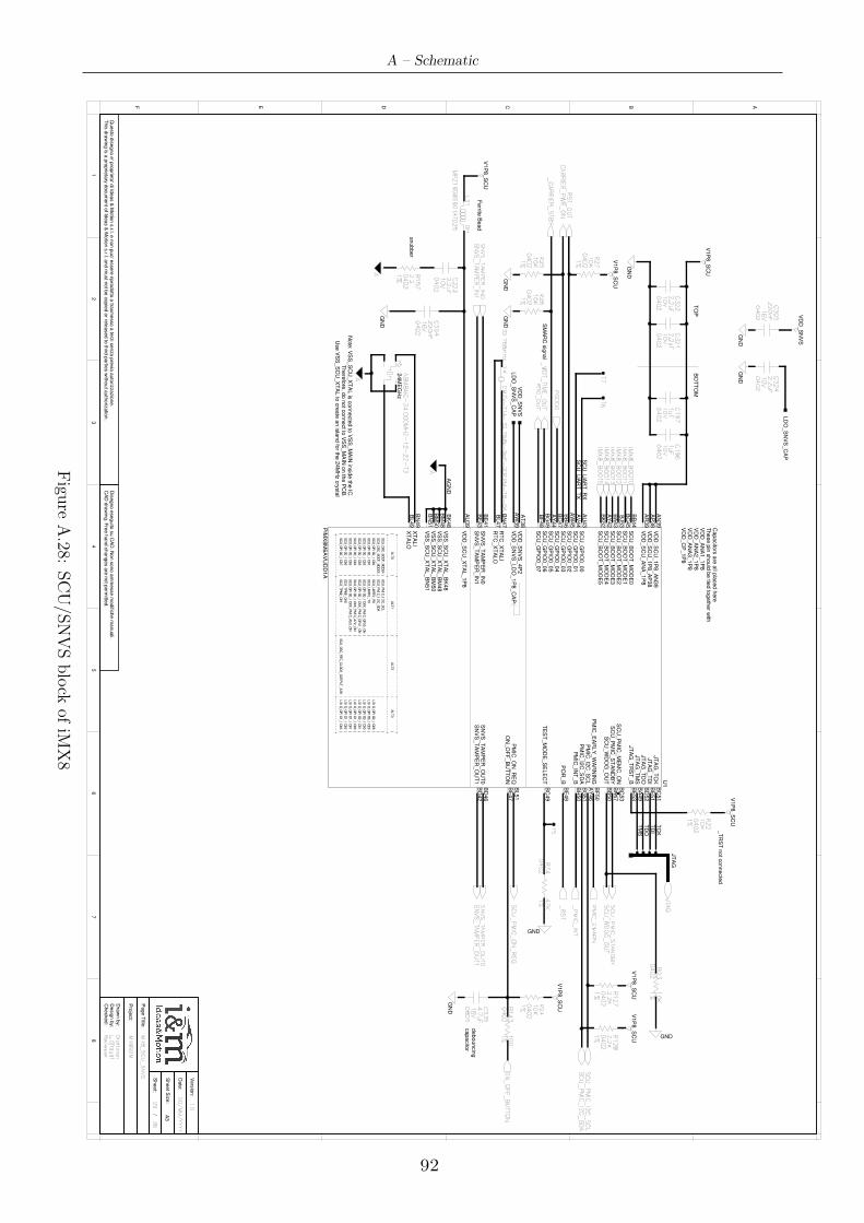
A – Schematic
Dra
wn b
y:
Checked:
Desig
n b
y:
Pro
ject:
Sheet S
ize:
Page T
itle:
Sheet:
Date
:
Vers
ion:
CA
D d
raw
ing. F
ree h
and c
hanges a
re n
ot p
erm
itted.
Dis
egno e
seguito
su C
AD
. Non s
ono a
mm
esse m
odific
he m
anuali.
This
dra
win
g is
a p
roprie
tary
docum
ent o
f Ideas &
Motio
n s
.r.l. and m
ust n
ot b
e c
opie
d o
r rele
ased to
third
partie
s w
ithout a
uth
oriz
atio
n.
Questo
dis
egno e
' pro
prie
ta' d
i Ideas &
Motio
n s
.r.l. e n
on p
uo' e
ssere
ripro
dotto
o tra
sm
esso a
terz
i senza p
revia
auto
rizzazio
ne.
/ A3
12
34
56
78
ABCDEF
Re
vie
we
r
Dra
ftma
n
iMX
8S
OM
1.0
IMX
8_
SC
U_
SN
VS
36
29
L. G
irau
di
DD
/M
M/
YY
YY
SC
U_
PM
IC_
STA
ND
BY
SC
U_
PM
IC_
ON
_R
EQ
SC
U_
WD
OG
_O
UT
SC
U_
PM
IC_
I2C
_S
DA
SC
U_
PM
IC_
I2C
_S
CL
_R
ST
PM
IC_
EW
AR
N
_P
MIC
_IN
T
Capacito
rs a
re a
ll pla
ced h
ere
These p
in s
hould
be tie
d to
geth
er w
ithV
DD
_A
NA
1_1P
8V
DD
_A
NA
2_1P
8V
DD
_A
NA
3_1P
8V
DD
_C
P_1P
8
R1
27
04
02
2.2
K
1%
1%
2.2
K0
40
2
R1
28
V1P
8_S
CU
V1P
8_S
CU
Y4
CM
7V
-T1
A-
32
.76
8k-
9p
F-
20
PP
M-
TB
-Q
A3
2.7
68
KH
z
Note
: VS
S_S
CU
_X
TA
L is
connecte
d to
VS
S_M
AIN
insid
e th
e IC
.T
here
fore
, do n
ot c
onnect to
VS
S_M
AIN
on th
e P
CB
.U
se V
SS
_S
CU
_X
TA
L to
cre
ate
an is
land fo
r the 2
4M
Hz c
rysta
l
C3
21
04
02
2.2
uF
10
V1
0V
2.2
uF
04
02
C3
22
C1
96
04
02
1u
F1
0V
10
V1
uF
04
02
C1
97
BO
TT
OM
TO
P
V1P
8_S
CU
GN
D
Y5
AB
M8
AIG
-2
4.0
00
MH
Z-
12
-2
Z-
T3
24M
EG
Hz
A
AG
ND
A
V1P
8_S
CU
C3
23
04
02
2.2
uF
10
V
A
C3
04
04
02
22
0n
F1
6V
L3
1
MP
Z1
60
8S
60
1A
TD
25 0H
Ferrite
Bead
ON
_O
FF
_B
UTTO
N
C3
35
08
05
4.7
uF
16
V
GN
D
debouncin
gcapacito
r
SN
VS
_TA
MP
ER
_O
UT1
SN
VS
_TA
MP
ER
_O
UT0
SN
VS
_TA
MP
ER
_IN
1S
NV
S_
TA
MP
ER
_IN
0
PG
OO
D
GN
D
LD
O_S
NV
S_C
AP
VD
D_S
NV
S
16
V2
20
nF
04
02
C3
05
C3
24
04
02
2.2
uF
10
V
GN
D
CA
RR
IER
_P
WR
_O
N
_C
AR
RIE
R_
STB
Y
1%
10
K0
40
2
R2
2
V1P
8_S
CU
JTA
GJT
AG
TM
S
TC
K
TD
OT
DI
SC
U_U
AR
T_R
XS
CU
_U
AR
T_T
X
_T
RS
T n
ot c
onnecte
d
RTC
_O
UT
1%
47
K0
40
2R
74
GND
T5
R2
30
40
21
0K
1%
GND
LD
O_S
NV
S_C
AP
VD
D_S
NV
S
GN
D SM
AR
C s
ignal
R1
57
04
02
2.2
1%
R1
43
04
02
10
01
%
R2
4
04
02
10
K
1%
V1P
8_S
CU
snubber
GN
D
1%
04
02
R2
51
0K
IMX
8_
BO
OT5
IMX
8_
BO
OT4
IMX
8_
BO
OT3
IMX
8_
BO
OT2
IMX
8_
BO
OT1
IMX
8_
BO
OT0
JT
AG
_T
CK
JT
AG
_T
DI
JT
AG
_T
DO
JT
AG
_T
MS
JT
AG
_T
RS
T_B
ON
_O
FF
_B
UT
TO
N
PM
IC_E
AR
LY
_W
AR
NIN
GP
MIC
_I2
C_S
CL
PM
IC_I2
C_S
DA
PM
IC_IN
T_B
PM
IC_O
N_R
EQ
PO
R_B
RT
C_X
TA
LI
RT
C_X
TA
LO
SC
U_B
OO
T_M
OD
E0
SC
U_B
OO
T_M
OD
E1
SC
U_B
OO
T_M
OD
E2
SC
U_B
OO
T_M
OD
E3
SC
U_B
OO
T_M
OD
E4
SC
U_B
OO
T_M
OD
E5
SC
U_G
PIO
0_00
SC
U_G
PIO
0_01
SC
U_G
PIO
0_02
SC
U_G
PIO
0_03
SC
U_G
PIO
0_04
SC
U_G
PIO
0_05
SC
U_G
PIO
0_06
SC
U_G
PIO
0_07
SN
VS
_T
AM
PE
R_IN
0S
NV
S_T
AM
PE
R_IN
1S
NV
S_T
AM
PE
R_O
UT
0S
NV
S_T
AM
PE
R_O
UT
1
VD
D_S
CU
_1P
8_A
N39
VD
D_S
CU
_1P
8_A
P38
VD
D_S
CU
_A
NA
_1P
8
VD
D_S
CU
_X
TA
L_1P
8
VD
D_S
NV
S_4P
2V
DD
_S
NV
S_LD
O_1P
8_C
AP
VS
S_S
CU
_X
TA
L_B
K48
VS
S_S
CU
_X
TA
L_B
M48
VS
S_S
CU
_X
TA
L_B
M50
VS
S_S
CU
_X
TA
L_B
N51
XT
ALI
XT
ALO
SC
U_P
MIC
_M
EM
C_O
NS
CU
_P
MIC
_S
TA
ND
BY
SC
U_W
DO
G_O
UT
TE
ST
_M
OD
E_S
ELE
CT
+-
--
--
--
--
--
--
--
--
--
-+
--
--
--
--
--
--
--
--
--
--
--
--
--
--
-+
--
--
--
--
--
--
--
--
--
--
--
--
--
--
--
+-
--
--
--
--
--
--
--
--
+
|
A
LT
0
|
AL
T1
|
A
LT
2
|
A
LT
3
|
+-
--
--
--
--
--
--
--
--
--
-+
--
--
--
--
--
--
--
--
--
--
--
--
--
--
-+
--
--
--
--
--
--
--
--
--
--
--
--
--
--
--
+-
--
--
--
--
--
--
--
--
+
|
SC
U_
DS
C_
BO
OT
_M
OD
E4
|
S
CU
_P
MI
C_
I2
C_
SC
L
|
|
|
|
SC
U_
DS
C_
BO
OT
_M
OD
E5
|
S
CU
_P
MI
C_
I2
C_
SD
A
|
|
|
|
SC
U_
GP
IO
0_
IO
00
|
S
CU
_U
AR
T0
_R
X
|
|
LS
IO
_G
PI
O0
_I
O2
8
|
|
SC
U_
GP
IO
0_
IO
01
|
S
CU
_U
AR
T0
_T
X
|
|
LS
IO
_G
PI
O0
_I
O2
9
|
|
SC
U_
GP
IO
0_
IO
02
|
S
CU
_G
PI
O0
_I
OX
X_
PM
IC
_G
PU
0_
ON
|
|
LS
IO
_G
PI
O0
_I
O3
0
|
|
SC
U_
GP
IO
0_
IO
03
|
S
CU
_G
PI
O0
_I
OX
X_
PM
IC
_G
PU
1_
ON
|
|
LS
IO
_G
PI
O0
_I
O3
1
|
|
SC
U_
GP
IO
0_
IO
04
|
S
CU
_G
PI
O0
_I
OX
X_
PM
IC
_A
72
_O
N
|
|
LS
IO
_G
PI
O1
_I
O0
0
|
|
SC
U_
GP
IO
0_
IO
05
|
S
CU
_G
PI
O0
_I
OX
X_
PM
IC
_A
53
_O
N
|
|
LS
IO
_G
PI
O1
_I
O0
1
|
|
SC
U_
GP
IO
0_
IO
06
|
S
CU
_T
PM
0_
CH
0
|
|
LS
IO
_G
PI
O1
_I
O0
2
|
|
SC
U_
GP
IO
0_
IO
07
|
S
CU
_T
PM
0_
CH
1
|
S
CU
_D
SC
_R
TC
_C
LO
CK
_O
UT
PU
T_
32
K
|
LS
IO
_G
PI
O1
_I
O0
3
|
+-
--
--
--
--
--
--
--
--
--
-+
--
--
--
--
--
--
--
--
--
--
--
--
--
--
-+
--
--
--
--
--
--
--
--
--
--
--
--
--
--
--
+-
--
--
--
--
--
--
--
--
+
U1
BC
49
BB
50
BA
47
BC
53
BL49
BN
49
BN
51
BM
50
BM
48
BK
48
AW
39
AT
38
AU
39
AR
39
AP
38
AN
39
BD
42
BD
46
BE
43
BE
41
BF
48
BG
49
AY
44
BC
47
BB
46
AW
45
AV
44
AU
43
BK
52
AY
42
BA
43
BJ53
BC
45
BB
44
BL47
BN
47
BE
49
BL51
BH
50
BG
51
AY
46
BF
50
BE
47
BE
53
BA
49
BD
52
BE
51
BC
51
PIM
X8M
6A
VU
DD
1A
GN
D
10
KR
26
04
02
1%
_R
ST_
OU
T
04
02
10
KR
27
1%
V1P
8_S
CU
T6
T7
_W
DT_
TIM
E_
OU
T
Figu
reA.28:
SCU/S
NVSblock
ofiM
X8
92
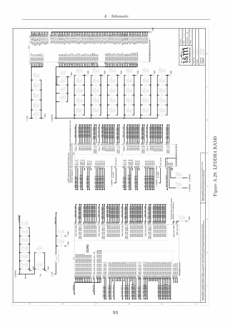
A – Schematic
Dra
wn b
y:
Checked:
Desig
n b
y:
Pro
ject:
Sheet S
ize:
Page T
itle
:
Sheet:
Date
:
Vers
ion:
CA
D d
raw
ing. F
ree h
and c
hanges a
re n
ot perm
itte
d.
Dis
egno e
seguito s
u C
AD
. N
on s
ono a
mm
esse m
odific
he m
anuali.
This
dra
win
g is a
pro
prieta
ry d
ocum
ent of Id
eas &
Motion s
.r.l. and m
ust not be c
opie
d o
r re
leased to third p
art
ies w
ithout auth
orization.
Questo
dis
egno e
' pro
prieta
' di Id
eas &
Motion s
.r.l. e n
on p
uo' e
ssere
rip
rodotto o
tra
sm
esso a
terz
i senza p
revia
auto
rizzazio
ne.
/A3
12
34
56
78
A B C D E F
1.0
DD
/M
M/
YY
YY
LP
DD
R4
-0
Re
vie
we
r
Dra
ftm
an
iMX
8S
OM
L.
Gir
au
di
30
36
DN
U_B
1D
NU
_A
B2
DN
U_A
B12
DN
U_A
B11
DN
U_A
B1
DN
U_A
A12
DN
U_A
A1
DN
U_A
2D
NU
_A
12
DN
U_A
11
DN
U_A
1
VS
S_C
8V
SS
_Y
8V
SS
_Y
5V
SS
_Y
12
VS
S_Y
1V
SS
_W
9V
SS
_W
4V
SS
_W
2V
SS
_W
11
VS
S_V
8V
SS
_V
5V
SS
_V
12
VS
S_V
1V
SS
_T
8V
SS
_T
5V
SS
_T
3V
SS
_T
12
VS
S_T
10
VS
S_T
1V
SS
_P
3V
SS
_P
12
VS
S_P
10
VS
S_P
1V
SS
_N
9V
SS
_N
4V
SS
_N
2V
SS
_N
11
VS
S_K
9V
SS
_K
4V
SS
_K
2V
SS
_K
11
VS
S_J3
VS
S_J12
VS
S_J10
VS
S_J1
VS
S_G
8V
SS
_G
5V
SS
_G
3V
SS
_G
12
VS
S_G
10
VS
S_G
1V
SS
_A
10
VS
S_A
3V
SS
_A
B10
VS
S_A
B3
VS
S_A
B5
VS
S_A
B8
VS
S_C
1V
SS
_C
12
VS
S_C
5D
NU
_B
12
VS
S_D
11
VS
S_D
2V
SS
_D
4V
SS
_D
9V
SS
_E
1V
SS
_E
12
VS
S_E
5V
SS
_E
8
VD
DQ
_W
8V
DD
Q_W
5V
DD
Q_W
12
VD
DQ
_W
1V
DD
Q_U
3V
DD
Q_U
10
VD
DQ
_F
3V
DD
Q_F
10
VD
DQ
_D
8V
DD
Q_D
5V
DD
Q_D
12
VD
DQ
_D
1V
DD
Q_B
8V
DD
Q_B
5V
DD
Q_B
3V
DD
Q_B
10
VD
DQ
_A
A8
VD
DQ
_A
A5
VD
DQ
_A
A3
VD
DQ
_A
A10
VD
D2_U
8V
DD
2_U
5V
DD
2_R
8V
DD
2_R
5V
DD
2_R
12
VD
D2_R
1V
DD
2_N
3V
DD
2_N
12
VD
D2_N
10
VD
D2_N
1V
DD
2_K
3V
DD
2_K
12
VD
D2_K
10
VD
D2_K
1V
DD
2_H
8V
DD
2_H
5V
DD
2_H
12
VD
D2_H
1V
DD
2_F
8V
DD
2_F
5V
DD
2_A
B9
VD
D2_A
B4
VD
D2_A
9V
DD
2_A
4
VD
D1_U
12
VD
D1_U
1V
DD
1_T
9V
DD
1_T
4V
DD
1_G
9V
DD
1_G
4V
DD
1_F
12
VD
D1_F
1
U11
F1
F12
G4
G9
T4
T9
U1
U12
A4
A9
AB
4A
B9
F5
F8
H1
H12
H5
H8
K1
K10
K12
K3
N1
N10
N12
N3
R1
R12
R5
R8
U5
U8
AA
10
AA
3A
A5
AA
8B
10
B3
B5
B8
D1
D12
D5
D8
F10
F3
U10
U3
W1
W12
W5
W8
E8
E5
E12
E1
D9
D4
D2
D11
B12
C5
C12
C1
AB
8A
B5
AB
3A
B10
A3
A10
G1
G10
G12
G3
G5
G8
J1
J10
J12
J3
K11
K2
K4
K9
N11
N2
N4
N9
P1
P10
P12
P3
T1
T10
T12
T3
T5
T8
V1
V12
V5
V8
W11
W2
W4
W9
Y1
Y12
Y5
Y8
C8
A1
A11
A12
A2
AA
1A
A12
AB
1A
B11
AB
12
AB
2B
1
MT
53B
768M
32D
4N
Q-0
62 A
AT
:B
CA
0_A
CA
1_A
CA
2_A
CA
3_A
CA
4_A
CA
5_A
CK
_T
_A
CK
E0_A
CK
E1_A
CK
E2_A
CS
0_A
CS
1_A
CS
2_A
CA
0_B
CA
1_B
CA
2_B
CA
3_B
CA
4_B
CA
5_B
CK
_T
_B
CK
E0_B
CK
E1_B
CK
E2_B
CS
0_B
CS
1_B
CS
2_B
DM
I0_A
DM
I1_A
DQ
0_A
DQ
1_A
DQ
2_A
DQ
3_A
DQ
4_A
DQ
5_A
DQ
6_A
DQ
7_A
DQ
8_A
DQ
9_A
DQ
10_A
DQ
11_A
DQ
12_A
DQ
13_A
DQ
14_A
DQ
15_A
DQ
S0_C
_A
DQ
S0_T
_A
DQ
S1_C
_A
DQ
S1_T
_A
DM
I0_B
DM
I1_B
DQ
0_B
DQ
1_B
DQ
2_B
DQ
3_B
DQ
4_B
DQ
5_B
DQ
6_B
DQ
7_B
DQ
8_B
DQ
9_B
DQ
10_B
DQ
11_B
DQ
12_B
DQ
13_B
DQ
14_B
DQ
15_B
DQ
S0_C
_B
DQ
S0_T
_B
DQ
S1_C
_B
DQ
S1_T
_B
OD
T_C
A_A
OD
T_C
A_B
RE
SE
T_N
ZQ
0Z
Q1
ZQ
2
CK
_C
_B
CK
_C
_A
U11
J9
P9
G11
A8
A5
T11
T2
G2
W10
V10
W3
V3
AA
9Y
9V
9U
9U
11
V11
Y11
AA
11
AA
4Y
4V
4U
4U
2V
2Y
2A
A2
Y10
Y3
D10
E10
D3
E3
B9
C9
E9
F9
F11
E11
C11
B11
B4
C4
E4
F4
F2
E2
C2
B2
C10
C3
N5
R3
R4
N8
P5
P4
P8
P11
R11
R10
R9
P2
R2
K5
H3
H4
K8
J5
J4
J8
J11
H11
H10
H9
J2
H2
MT
53B
768M
32D
4N
Q-0
62 A
AT
:B
VD
D_D
DR
_C
H0_V
DD
A_P
LL_1P
8
DD
R_C
H0_Z
Q
DD
R_C
H0_V
RE
FD
DR
_C
H0_D
TO
1D
DR
_C
H0_D
TO
0
DD
R_C
H0_A
TO
DD
R_C
H0_C
K1_P
DD
R_C
H0_C
K1_N
DD
R_C
H0_C
K0_P
DD
R_C
H0_C
K0_N
DD
R_C
H0_D
QS
3_P
DD
R_C
H0_D
QS
3_N
DD
R_C
H0_D
QS
2_P
DD
R_C
H0_D
QS
2_N
DD
R_C
H0_D
QS
1_P
DD
R_C
H0_D
QS
1_N
DD
R_C
H0_D
QS
0_P
DD
R_C
H0_D
QS
0_N
DD
R_C
H0_D
M3
DD
R_C
H0_D
M2
DD
R_C
H0_D
M1
DD
R_C
H0_D
M0
VD
D_D
DR
_C
H0_V
DD
Q_A
A39
VD
D_D
DR
_C
H0_V
DD
Q_A
E39
VD
D_D
DR
_C
H0_V
DD
Q_A
F38
VD
D_D
DR
_C
H0_V
DD
Q_A
G39
VD
D_D
DR
_C
H0_V
DD
Q_A
H38
VD
D_D
DR
_C
H0_V
DD
Q_A
J39
VD
D_D
DR
_C
H0_V
DD
Q_C
KE
_A
B38
VD
D_D
DR
_C
H0_V
DD
Q_C
KE
_A
C39
VD
D_D
DR
_C
H0_V
DD
Q_C
KE
_A
D38
VD
D_D
DR
_C
H0_V
DD
Q_U
39
VD
D_D
DR
_C
H0_V
DD
Q_V
38
VD
D_D
DR
_C
H0_V
DD
Q_W
39
VD
D_D
DR
_C
H0_V
DD
Q_Y
38
DD
R_C
H0_D
CF
00
DD
R_C
H0_D
CF
01
DD
R_C
H0_D
CF
02
DD
R_C
H0_D
CF
03
DD
R_C
H0_D
CF
04
DD
R_C
H0_D
CF
05
DD
R_C
H0_D
CF
06
DD
R_C
H0_D
CF
07
DD
R_C
H0_D
CF
08
DD
R_C
H0_D
CF
09
DD
R_C
H0_D
CF
10
DD
R_C
H0_D
CF
11
DD
R_C
H0_D
CF
12
DD
R_C
H0_D
CF
13
DD
R_C
H0_D
CF
14
DD
R_C
H0_D
CF
15
DD
R_C
H0_D
CF
16
DD
R_C
H0_D
CF
17
DD
R_C
H0_D
CF
18
DD
R_C
H0_D
CF
19
DD
R_C
H0_D
CF
20
DD
R_C
H0_D
CF
21
DD
R_C
H0_D
CF
22
DD
R_C
H0_D
CF
23
DD
R_C
H0_D
CF
24
DD
R_C
H0_D
CF
25
DD
R_C
H0_D
CF
26
DD
R_C
H0_D
CF
27
DD
R_C
H0_D
CF
28
DD
R_C
H0_D
CF
29
DD
R_C
H0_D
CF
30
DD
R_C
H0_D
CF
31
DD
R_C
H0_D
CF
32
DD
R_C
H0_D
CF
33
DD
R_C
H0_D
Q00
DD
R_C
H0_D
Q01
DD
R_C
H0_D
Q02
DD
R_C
H0_D
Q03
DD
R_C
H0_D
Q04
DD
R_C
H0_D
Q05
DD
R_C
H0_D
Q06
DD
R_C
H0_D
Q07
DD
R_C
H0_D
Q08
DD
R_C
H0_D
Q09
DD
R_C
H0_D
Q10
DD
R_C
H0_D
Q11
DD
R_C
H0_D
Q12
DD
R_C
H0_D
Q13
DD
R_C
H0_D
Q14
DD
R_C
H0_D
Q15
DD
R_C
H0_D
Q16
DD
R_C
H0_D
Q17
DD
R_C
H0_D
Q18
DD
R_C
H0_D
Q19
DD
R_C
H0_D
Q20
DD
R_C
H0_D
Q21
DD
R_C
H0_D
Q22
DD
R_C
H0_D
Q23
DD
R_C
H0_D
Q24
DD
R_C
H0_D
Q25
DD
R_C
H0_D
Q26
DD
R_C
H0_D
Q27
DD
R_C
H0_D
Q28
DD
R_C
H0_D
Q29
DD
R_C
H0_D
Q30
DD
R_C
H0_D
Q31
DD
R0
U1
AR
51
AJ43
AP
50
AR
53
AL47
AM
48
AH
44
AJ45
AH
50
AH
48
AH
46
AJ49
AJ51
AL51
AL49
AM
50
P48
P50
N49
P46
L51
N51
K50
L49
N43
G51
G53
H50
K48
L47
N45
P44
AF
48
AE
53
AB
52
AC
53
AE
49
AF
50
AE
51
AE
47
AF
52
AB
44
AC
45
AC
51
AE
45
AC
43
AB
46
AB
48
AC
47
U53
Y52
W53
T46
U49
U51
T50
T52
T48
W51
W45
Y44
W43
Y46
Y48
W47
U47
Y38
W39
V38
U39
AD
38
AC
39
AB
38
AJ39
AH
38
AG
39
AF
38
AE
39
AA
39
H52
N47
AJ47
AP
52
L53
K52
P52
N53
AH
52
AJ53
AL53
AM
52
Y50
W49
AB
50
AC
49
AF
46
U45
T44
U43
AF
44
AE
43
PIM
X8M
6A
VU
DD
1A
C1
80
04
02
1u
F1
0V
10
V1
uF
04
02
C1
81
10
V1
uF
04
02
C1
82
C1
83
04
02
1u
F1
0V
10
V1
uF
04
02
C1
84
C1
85
04
02
1u
F1
0V
GN
D
Bottom
Top
C4
12
10
22
uF
16
V1
6V
22
uF
12
10
C5
GN
D
V_D
DR
IO0
V_D
DR
IO0
C1
86
04
02
1u
F1
0V
C3
19
04
02
2.2
uF
10
V
L2 BLM
18
EG
60
1S
N1
0H
GN
DG
ND
V_1P
8
R1
44
04
02
24
0
1%
GN
D
C6
12
10
22
uF
16
V
C2
35
04
02
22
0n
F1
6V
16
V2
20
nF
04
02
C2
36
C2
37
04
02
22
0n
F1
6V
16
V2
20
nF
04
02
C2
38
GN
D
V_1P
8
16
V2
2u
F
12
10
C7
C8
12
10
22
uF
16
V1
6V
22
uF
12
10
C9
C1
0
12
10
22
uF
16
V
C2
39
04
02
22
0n
F1
6V
16
V2
20
nF
04
02
C2
40
16
V2
20
nF
04
02
C2
41
16
V2
20
nF
04
02
C2
42
16
V2
20
nF
04
02
C2
43
16
V2
20
nF
04
02
C2
44
16
V2
20
nF
04
02
C2
45
16
V2
20
nF
04
02
C2
46
16
V2
20
nF
04
02
C2
47
16
V2
20
nF
04
02
C2
48
16
V2
20
nF
04
02
C2
49
16
V2
20
nF
04
02
C2
50
16
V2
20
nF
04
02
C2
51
16
V2
20
nF
04
02
C2
52
16
V2
20
nF
04
02
C2
53
16
V2
20
nF
04
02
C2
54
16
V2
20
nF
04
02
C2
55
16
V2
20
nF
04
02
C2
56
16
V2
20
nF
04
02
C2
57
16
V2
20
nF
04
02
C2
58
16
V2
20
nF
04
02
C2
59
16
V2
20
nF
04
02
C2
60
16
V2
20
nF
04
02
C2
61
16
V2
20
nF
04
02
C2
62
16
V2
20
nF
04
02
C2
63
16
V2
20
nF
04
02
C2
64
16
V2
20
nF
04
02
C2
65
16
V2
20
nF
04
02
C2
66
16
V2
20
nF
04
02
C2
67
16
V2
20
nF
04
02
C2
68
GN
D GN
D
GN
D
GN
D
GN
D
GN
D
GN
D
V_D
DR
IO0
V_D
DR
IO0
GN
D
DD
R_C
H0_D
Q0
DD
R_C
H0_D
Q1
DD
R_C
H0_D
Q2
DD
R_C
H0_D
Q3
DD
R_C
H0_D
Q4
DD
R_C
H0_D
Q5
DD
R_C
H0_D
Q6
DD
R_C
H0_D
Q7
DD
R_C
H0_D
Q8
DD
R_C
H0_D
Q9
DD
R_C
H0_D
Q10
DD
R_C
H0_D
Q11
DD
R_C
H0_D
Q12
DD
R_C
H0_D
Q13
DD
R_C
H0_D
Q14
DD
R_C
H0_D
Q15
DD
R_C
H0_D
Q16
DD
R_C
H0_D
Q17
DD
R_C
H0_D
Q18
DD
R_C
H0_D
Q19
DD
R_C
H0_D
Q20
DD
R_C
H0_D
Q21
DD
R_C
H0_D
Q22
DD
R_C
H0_D
Q23
DD
R_C
H0_D
Q24
DD
R_C
H0_D
Q25
DD
R_C
H0_D
Q26
DD
R_C
H0_D
Q27
DD
R_C
H0_D
Q28
DD
R_C
H0_D
Q29
DD
R_C
H0_D
Q30
DD
R_C
H0_D
Q31
DD
R_C
H0_D
QS
0+
DD
R_C
H0_D
QS
1+
DD
R_C
H0_D
QS
2+
DD
R_C
H0_D
QS
3+
DD
R_C
H0_D
QS
0-
DD
R_C
H0_D
QS
1-
DD
R_C
H0_D
QS
2-
DD
R_C
H0_D
QS
3-
DD
R_C
H0_D
M0
DD
R_C
H0_D
M1
DD
R_C
H0_D
M2
DD
R_C
H0_D
M3
DD
R_C
H0_D
QS
0+
DD
R_C
H0_D
QS
0-
DD
R_C
H0_D
QS
1+
DD
R_C
H0_D
QS
1-
DD
R_C
H0_D
QS
2+
DD
R_C
H0_D
QS
2-
DD
R_C
H0_D
QS
3+
DD
R_C
H0_D
QS
3-
DD
R_C
H0_D
M0
DD
R_C
H0_D
M1
DD
R_C
H0_D
M2
DD
R_C
H0_D
M3
DD
R_C
H0_C
K1+
DD
R_C
H0_C
K1-
DD
R_C
H0_C
K0+
DD
R_C
H0_C
K0-
LP
4_C
H0_C
A0_A
LP
4_C
H0_C
A1_A
LP
4_C
H0_C
A2_A
LP
4_C
H0_C
A3_A
LP
4_C
H0_C
A4_A
LP
4_C
H0_C
A5_A
LP
4_C
H0_C
S0_A
LP
4_C
H0_C
S1_A
LP
4_C
H0_C
KE
1_A
LP
4_C
H0_C
KE
0_A
LP
4_C
H0_C
A0_B
LP
4_C
H0_C
A1_B
LP
4_C
H0_C
A2_B
LP
4_C
H0_C
A3_B
LP
4_C
H0_C
A4_B
LP
4_C
H0_C
A5_B
LP
4_C
H0_C
S0_B
LP
4_C
H0_C
S1_B
LP
4_C
H0_C
KE
1_B
LP
4_C
H0_C
KE
0_B
_LP
4_C
H0_R
ES
ET
DD
R_C
H0_C
K0+
DD
R_C
H0_C
K0-
DD
R_C
H0_C
K1+
DD
R_C
H0_C
K1-
LP
4_C
H0_C
KE
1_A
LP
4_C
H0_C
KE
0_A
LP
4_C
H0_C
KE
1_B
LP
4_C
H0_C
KE
0_B
LP
4_C
H0_C
S0_A
LP
4_C
H0_C
S1_A
LP
4_C
H0_C
S0_B
LP
4_C
H0_C
S1_B
LP
4_C
H0_C
A0_A
LP
4_C
H0_C
A3_A
LP
4_C
H0_C
A1_A
LP
4_C
H0_C
A2_A
LP
4_C
H0_C
A4_A
LP
4_C
H0_C
A5_A
LP
4_C
H0_C
A4_B
LP
4_C
H0_C
A5_B
LP
4_C
H0_C
A3_B
LP
4_C
H0_C
A0_B
LP
4_C
H0_C
A1_B
LP
4_C
H0_C
A2_B
_LP
4_C
H0_R
ES
ET
VD
DA
_P
LL
VD
DA
_P
LL
V_D
DR
IO0
Imx8M
"H
ard
ware
develo
pm
ent's
Guid
e"
says
"Byte
sw
appin
g w
ithin
each 1
6-b
it c
hannel is
OK
. B
it s
wappin
g w
ithin
each s
lice/b
yte
lane is O
K."
Consid
er
sw
appin
g in o
rder
to a
void
cro
ssin
g in the b
us lin
es.
On d
ie term
ination
for
rankA
On d
ie term
ination
for
rankB
On E
VB
, th
ere
is a
n R
C n
etw
ork
labele
d a
s "
not necessary
".
R1
45
04
02
24
0
1%
R1
46
04
02
24
0
1%
V_D
DR
IO0
V_D
DR
IO0
V_D
DR
IO0
V_D
DR
IO0
Figure
A.29:
LPDDR4RAM0
93
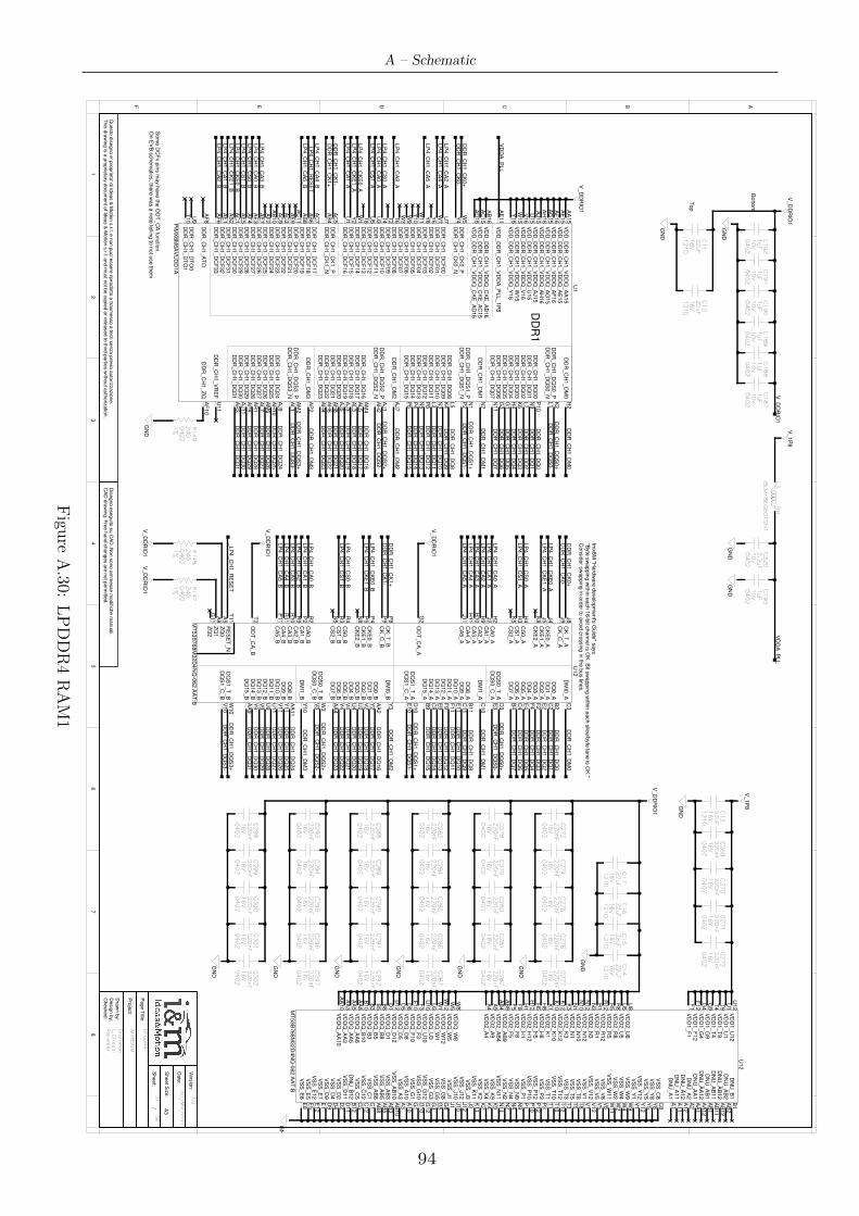
A – Schematic
CA
0_A
CA
1_A
CA
2_A
CA
3_A
CA
4_A
CA
5_A
CK
_T
_A
CK
E0_A
CK
E1_A
CK
E2_A
CS
0_A
CS
1_A
CS
2_A
CA
0_B
CA
1_B
CA
2_B
CA
3_B
CA
4_B
CA
5_B
CK
_T
_B
CK
E0_B
CK
E1_B
CK
E2_B
CS
0_B
CS
1_B
CS
2_B
DM
I0_A
DM
I1_A
DQ
0_A
DQ
1_A
DQ
2_A
DQ
3_A
DQ
4_A
DQ
5_A
DQ
6_A
DQ
7_A
DQ
8_A
DQ
9_A
DQ
10_A
DQ
11_A
DQ
12_A
DQ
13_A
DQ
14_A
DQ
15_A
DQ
S0_C
_A
DQ
S0_T
_A
DQ
S1_C
_A
DQ
S1_T
_A
DM
I0_B
DM
I1_B
DQ
0_B
DQ
1_B
DQ
2_B
DQ
3_B
DQ
4_B
DQ
5_B
DQ
6_B
DQ
7_B
DQ
8_B
DQ
9_B
DQ
10_B
DQ
11_B
DQ
12_B
DQ
13_B
DQ
14_B
DQ
15_B
DQ
S0_C
_B
DQ
S0_T
_B
DQ
S1_C
_B
DQ
S1_T
_B
OD
T_C
A_A
OD
T_C
A_B
RE
SE
T_N
ZQ
0Z
Q1
ZQ
2
CK
_C
_B
CK
_C
_A
U12
J9
P9
G11
A8
A5
T11
T2
G2
W10
V10
W3
V3
AA
9Y
9V
9U
9U
11
V11
Y11
AA
11
AA
4Y
4V
4U
4U
2V
2Y
2A
A2
Y10
Y3
D10
E10
D3
E3
B9
C9
E9
F9
F11
E11
C11
B11
B4
C4
E4
F4
F2
E2
C2
B2
C10
C3
N5
R3
R4
N8
P5
P4
P8
P11
R11
R10
R9
P2
R2
K5
H3
H4
K8
J5
J4
J8
J11
H11
H10
H9
J2
H2
MT
53B
768M
32D
4N
Q-0
62 A
AT
:B
DN
U_B
1D
NU
_A
B2
DN
U_A
B12
DN
U_A
B11
DN
U_A
B1
DN
U_A
A12
DN
U_A
A1
DN
U_A
2D
NU
_A
12
DN
U_A
11
DN
U_A
1
VS
S_C
8V
SS
_Y
8V
SS
_Y
5V
SS
_Y
12
VS
S_Y
1V
SS
_W
9V
SS
_W
4V
SS
_W
2V
SS
_W
11
VS
S_V
8V
SS
_V
5V
SS
_V
12
VS
S_V
1V
SS
_T
8V
SS
_T
5V
SS
_T
3V
SS
_T
12
VS
S_T
10
VS
S_T
1V
SS
_P
3V
SS
_P
12
VS
S_P
10
VS
S_P
1V
SS
_N
9V
SS
_N
4V
SS
_N
2V
SS
_N
11
VS
S_K
9V
SS
_K
4V
SS
_K
2V
SS
_K
11
VS
S_J3
VS
S_J12
VS
S_J10
VS
S_J1
VS
S_G
8V
SS
_G
5V
SS
_G
3V
SS
_G
12
VS
S_G
10
VS
S_G
1V
SS
_A
10
VS
S_A
3V
SS
_A
B10
VS
S_A
B3
VS
S_A
B5
VS
S_A
B8
VS
S_C
1V
SS
_C
12
VS
S_C
5D
NU
_B
12
VS
S_D
11
VS
S_D
2V
SS
_D
4V
SS
_D
9V
SS
_E
1V
SS
_E
12
VS
S_E
5V
SS
_E
8
VD
DQ
_W
8V
DD
Q_W
5V
DD
Q_W
12
VD
DQ
_W
1V
DD
Q_U
3V
DD
Q_U
10
VD
DQ
_F
3V
DD
Q_F
10
VD
DQ
_D
8V
DD
Q_D
5V
DD
Q_D
12
VD
DQ
_D
1V
DD
Q_B
8V
DD
Q_B
5V
DD
Q_B
3V
DD
Q_B
10
VD
DQ
_A
A8
VD
DQ
_A
A5
VD
DQ
_A
A3
VD
DQ
_A
A10
VD
D2_U
8V
DD
2_U
5V
DD
2_R
8V
DD
2_R
5V
DD
2_R
12
VD
D2_R
1V
DD
2_N
3V
DD
2_N
12
VD
D2_N
10
VD
D2_N
1V
DD
2_K
3V
DD
2_K
12
VD
D2_K
10
VD
D2_K
1V
DD
2_H
8V
DD
2_H
5V
DD
2_H
12
VD
D2_H
1V
DD
2_F
8V
DD
2_F
5V
DD
2_A
B9
VD
D2_A
B4
VD
D2_A
9V
DD
2_A
4
VD
D1_U
12
VD
D1_U
1V
DD
1_T
9V
DD
1_T
4V
DD
1_G
9V
DD
1_G
4V
DD
1_F
12
VD
D1_F
1
U12
F1
F12
G4
G9
T4
T9
U1
U12
A4
A9
AB
4A
B9
F5
F8
H1
H12
H5
H8
K1
K10
K12
K3
N1
N10
N12
N3
R1
R12
R5
R8
U5
U8
AA
10
AA
3A
A5
AA
8B
10
B3
B5
B8
D1
D12
D5
D8
F10
F3
U10
U3
W1
W12
W5
W8
E8
E5
E12
E1
D9
D4
D2
D11
B12
C5
C12
C1
AB
8A
B5
AB
3A
B10
A3
A10
G1
G10
G12
G3
G5
G8
J1
J10
J12
J3
K11
K2
K4
K9
N11
N2
N4
N9
P1
P10
P12
P3
T1
T10
T12
T3
T5
T8
V1
V12
V5
V8
W11
W2
W4
W9
Y1
Y12
Y5
Y8
C8
A1
A11
A12
A2
AA
1A
A12
AB
1A
B11
AB
12
AB
2B
1
MT
53B
768M
32D
4N
Q-0
62 A
AT
:B
Dra
wn b
y:
Checked:
Desig
n b
y:
Pro
ject:
Sheet S
ize:
Page T
itle:
Sheet:
Date
:
Vers
ion:
CA
D d
raw
ing. F
ree h
and c
hanges a
re n
ot p
erm
itted.
Dis
egno e
seguito
su C
AD
. Non s
ono a
mm
esse m
odific
he m
anuali.
This
dra
win
g is
a p
roprie
tary
docum
ent o
f Ideas &
Motio
n s
.r.l. and m
ust n
ot b
e c
opie
d o
r rele
ased to
third
partie
s w
ithout a
uth
oriz
atio
n.
Questo
dis
egno e
' pro
prie
ta' d
i Ideas &
Motio
n s
.r.l. e n
on p
uo' e
ssere
ripro
dotto
o tra
sm
esso a
terz
i senza p
revia
auto
rizzazio
ne.
/ A3
12
34
56
78
ABCDEF
Re
vie
we
r
Dra
ftma
n
iMX
8S
OM
L. G
irau
di
31
36
1.0
DD
/M
M/
YY
YY
LP
DD
R4
VD
D_D
DR
_C
H1_V
DD
Q_A
A15
VD
D_D
DR
_C
H1_V
DD
Q_A
E15
VD
D_D
DR
_C
H1_V
DD
Q_A
F16
VD
D_D
DR
_C
H1_V
DD
Q_A
G15
VD
D_D
DR
_C
H1_V
DD
Q_A
H16
VD
D_D
DR
_C
H1_V
DD
Q_A
J15
VD
D_D
DR
_C
H1_V
DD
Q_C
KE
_A
B16
VD
D_D
DR
_C
H1_V
DD
Q_C
KE
_A
C15
VD
D_D
DR
_C
H1_V
DD
Q_C
KE
_A
D16
VD
D_D
DR
_C
H1_V
DD
Q_U
15
VD
D_D
DR
_C
H1_V
DD
Q_V
16
VD
D_D
DR
_C
H1_V
DD
Q_W
15
VD
D_D
DR
_C
H1_V
DD
Q_Y
16
VD
D_D
DR
_C
H1_V
DD
A_P
LL_1P
8
DD
R_C
H1_C
K0_N
DD
R_C
H1_C
K0_P
DD
R_C
H1_D
CF
00
DD
R_C
H1_D
CF
01
DD
R_C
H1_D
CF
02
DD
R_C
H1_D
CF
03
DD
R_C
H1_D
CF
04
DD
R_C
H1_D
CF
05
DD
R_C
H1_D
CF
06
DD
R_C
H1_D
CF
07
DD
R_C
H1_D
CF
08
DD
R_C
H1_D
CF
09
DD
R_C
H1_D
CF
10
DD
R_C
H1_D
CF
11
DD
R_C
H1_D
CF
12
DD
R_C
H1_D
CF
13
DD
R_C
H1_D
CF
14
DD
R_C
H1_D
CF
15
DD
R_C
H1_D
CF
16
DD
R_C
H1_C
K1_N
DD
R_C
H1_C
K1_P
DD
R_C
H1_D
CF
17
DD
R_C
H1_D
CF
18
DD
R_C
H1_D
CF
19
DD
R_C
H1_D
CF
20
DD
R_C
H1_D
CF
21
DD
R_C
H1_D
CF
22
DD
R_C
H1_D
CF
23
DD
R_C
H1_D
CF
24
DD
R_C
H1_D
CF
25
DD
R_C
H1_D
CF
26
DD
R_C
H1_D
CF
27
DD
R_C
H1_D
CF
28
DD
R_C
H1_D
CF
29
DD
R_C
H1_D
CF
30
DD
R_C
H1_D
CF
31
DD
R_C
H1_D
CF
32
DD
R_C
H1_D
CF
33
DD
R_C
H1_A
TO
DD
R_C
H1_D
TO
0D
DR
_C
H1_D
TO
1
DD
R_C
H1_D
M0
DD
R_C
H1_D
M1
DD
R_C
H1_D
M2
DD
R_C
H1_D
M3
DD
R_C
H1_D
Q00
DD
R_C
H1_D
Q01
DD
R_C
H1_D
Q02
DD
R_C
H1_D
Q03
DD
R_C
H1_D
Q04
DD
R_C
H1_D
Q05
DD
R_C
H1_D
Q06
DD
R_C
H1_D
Q07
DD
R_C
H1_D
QS
0_N
DD
R_C
H1_D
QS
0_P
DD
R_C
H1_D
QS
1_N
DD
R_C
H1_D
QS
1_P
DD
R_C
H1_D
QS
2_N
DD
R_C
H1_D
QS
2_P
DD
R_C
H1_D
QS
3_N
DD
R_C
H1_D
QS
3_P
DD
R_C
H1_D
Q08
DD
R_C
H1_D
Q09
DD
R_C
H1_D
Q10
DD
R_C
H1_D
Q11
DD
R_C
H1_D
Q12
DD
R_C
H1_D
Q13
DD
R_C
H1_D
Q14
DD
R_C
H1_D
Q15
DD
R_C
H1_D
Q16
DD
R_C
H1_D
Q17
DD
R_C
H1_D
Q18
DD
R_C
H1_D
Q19
DD
R_C
H1_D
Q20
DD
R_C
H1_D
Q21
DD
R_C
H1_D
Q22
DD
R_C
H1_D
Q23
DD
R_C
H1_D
Q24
DD
R_C
H1_D
Q25
DD
R_C
H1_D
Q26
DD
R_C
H1_D
Q27
DD
R_C
H1_D
Q28
DD
R_C
H1_D
Q29
DD
R_C
H1_D
Q30
DD
R_C
H1_D
Q31
DD
R_C
H1_V
RE
F
DD
R_C
H1_Z
Q
DD
R1
U1
AF
10
U11
AR
3A
J11
AP
4A
R1
AL7
AM
6A
H10
AJ9
AH
4A
H6
AH
8A
J5
AJ3
AL3
AL5
AM
4
P6
P4
N5
P8
L3
N3
K4
L5
AM
2A
L1
AJ1
AH
2
N1
P2
K2
L1
N11
G3
G1
H4
K6
L7
N9
P10
AP
2
AJ7
N7
H2
T10
U9
AF
8
AF
6A
E1
AB
2A
C1
AE
5A
F4
AE
3A
E7
AF
2A
B10
AC
9A
C3
AE
9A
C11
AB
8A
B6
AC
7
AC
5A
B4
U1
Y2
W1
T8
U5
U3
T4
T2
T6
W3
W9
Y10
W11
Y8
Y6
W7
U7
W5
Y4
AE
11
Y16
W15
V16
U15
AD
16
AC
15
AB
16
AJ15
AH
16
AG
15
AF
16
AE
15
AA
15
PIM
X8M
6A
VU
DD
1A
GN
D
GN
D
GN
DG
ND
Botto
m
Top
V_1P
8V
_D
DR
IO1
V_D
DR
IO1
DD
R_C
H1_C
K1+
DD
R_C
H1_C
K1-
DD
R_C
H1_C
K0+
DD
R_C
H1_C
K0-
LP
4_C
H1_C
A0_A
LP
4_C
H1_C
A1_A
LP
4_C
H1_C
A2_A
LP
4_C
H1_C
A3_A
LP
4_C
H1_C
A4_A
LP
4_C
H1_C
A5_A
LP
4_C
H1_C
S0_A
LP
4_C
H1_C
S1_A
LP
4_C
H1_C
KE
1_A
LP
4_C
H1_C
KE
0_A
LP
4_C
H1_C
A0_B
LP
4_C
H1_C
A1_B
LP
4_C
H1_C
A2_B
LP
4_C
H1_C
A3_B
LP
4_C
H1_C
A4_B
LP
4_C
H1_C
A5_B
LP
4_C
H1_C
S0_B
LP
4_C
H1_C
S1_B
LP
4_C
H1_C
KE
1_B
LP
4_C
H1_C
KE
0_B
_LP
4_C
H1_R
ES
ET
DD
R_C
H1_D
Q0
DD
R_C
H1_D
Q1
DD
R_C
H1_D
Q2
DD
R_C
H1_D
Q3
DD
R_C
H1_D
Q4
DD
R_C
H1_D
Q5
DD
R_C
H1_D
Q6
DD
R_C
H1_D
Q7
DD
R_C
H1_D
Q8
DD
R_C
H1_D
Q9
DD
R_C
H1_D
Q10
DD
R_C
H1_D
Q11
DD
R_C
H1_D
Q12
DD
R_C
H1_D
Q13
DD
R_C
H1_D
Q14
DD
R_C
H1_D
Q15
DD
R_C
H1_D
Q16
DD
R_C
H1_D
Q17
DD
R_C
H1_D
Q18
DD
R_C
H1_D
Q19
DD
R_C
H1_D
Q20
DD
R_C
H1_D
Q21
DD
R_C
H1_D
Q22
DD
R_C
H1_D
Q23
DD
R_C
H1_D
Q24
DD
R_C
H1_D
Q25
DD
R_C
H1_D
Q26
DD
R_C
H1_D
Q27
DD
R_C
H1_D
Q28
DD
R_C
H1_D
Q29
DD
R_C
H1_D
Q30
DD
R_C
H1_D
Q31
DD
R_C
H1_D
QS
0+
DD
R_C
H1_D
QS
1+
DD
R_C
H1_D
QS
2+
DD
R_C
H1_D
QS
3+
DD
R_C
H1_D
QS
0-
DD
R_C
H1_D
QS
1-
DD
R_C
H1_D
QS
2-
DD
R_C
H1_D
QS
3-
DD
R_C
H1_D
M0
DD
R_C
H1_D
M1
DD
R_C
H1_D
M2
DD
R_C
H1_D
M3
DD
R_C
H1_C
K0+
DD
R_C
H1_C
K0-
LP
4_C
H1_C
KE
1_A
LP
4_C
H1_C
KE
0_A
LP
4_C
H1_C
S0_A
LP
4_C
H1_C
S1_A
LP
4_C
H1_C
A0_A
LP
4_C
H1_C
A3_A
LP
4_C
H1_C
A1_A
LP
4_C
H1_C
A2_A
LP
4_C
H1_C
A4_A
LP
4_C
H1_C
A5_A
DD
R_C
H1_C
K1+
DD
R_C
H1_C
K1-
LP
4_C
H1_C
KE
1_B
LP
4_C
H1_C
KE
0_B
LP
4_C
H1_C
S0_B
LP
4_C
H1_C
S1_B
LP
4_C
H1_C
A4_B
LP
4_C
H1_C
A5_B
LP
4_C
H1_C
A3_B
LP
4_C
H1_C
A0_B
LP
4_C
H1_C
A1_B
LP
4_C
H1_C
A2_B
_LP
4_C
H1_R
ES
ET
DD
R_C
H1_D
Q0
DD
R_C
H1_D
Q1
DD
R_C
H1_D
Q2
DD
R_C
H1_D
Q3
DD
R_C
H1_D
Q4
DD
R_C
H1_D
Q5
DD
R_C
H1_D
Q6
DD
R_C
H1_D
Q7
DD
R_C
H1_D
Q8
DD
R_C
H1_D
Q9
DD
R_C
H1_D
Q10
DD
R_C
H1_D
Q11
DD
R_C
H1_D
Q12
DD
R_C
H1_D
Q13
DD
R_C
H1_D
Q14
DD
R_C
H1_D
Q15
DD
R_C
H1_D
Q16
DD
R_C
H1_D
Q17
DD
R_C
H1_D
Q18
DD
R_C
H1_D
Q19
DD
R_C
H1_D
Q20
DD
R_C
H1_D
Q21
DD
R_C
H1_D
Q22
DD
R_C
H1_D
Q23
DD
R_C
H1_D
Q24
DD
R_C
H1_D
Q25
DD
R_C
H1_D
Q26
DD
R_C
H1_D
Q27
DD
R_C
H1_D
Q28
DD
R_C
H1_D
Q29
DD
R_C
H1_D
Q30
DD
R_C
H1_D
Q31
DD
R_C
H1_D
QS
0+
DD
R_C
H1_D
QS
0-
DD
R_C
H1_D
QS
1+
DD
R_C
H1_D
QS
1-
DD
R_C
H1_D
QS
2+
DD
R_C
H1_D
QS
2-
DD
R_C
H1_D
QS
3+
DD
R_C
H1_D
QS
3-
DD
R_C
H1_D
M0
DD
R_C
H1_D
M1
DD
R_C
H1_D
M2
DD
R_C
H1_D
M3
GN
D
GN
DGN
D
GN
D
GN
D
GN
D
GN
D
GN
D
V_1P
8
GN
D
V_D
DR
IO1
V_D
DR
IO1
V_D
DR
IO1
V_D
DR
IO1
12
10
22
uF
16
V
C1
1
16
V2
2u
F
12
10
C1
2
C1
93
04
02
1u
F1
0V
C3
20
04
02
2.2
uF
10
V
BLM
18
EG
60
1S
N1
L3
0H
1u
F
04
02
C1
92
10
V
C1
91
04
02
1u
F1
0V
10
V1
uF
04
02
C1
90
C1
89
04
02
1u
F1
0V
04
02
1u
F1
0V
C1
88
10
V1
uF
04
02
C1
87
1%
24
00
40
2
R1
47
1%
24
0R
14
8
04
02
16
V2
2u
F
12
10
C1
3
16
V2
20
nF
04
02
C2
69
C2
94
04
02
22
0n
F1
6V
C2
95
04
02
22
0n
F1
6V
04
02
22
0n
F1
6V
C2
96
C2
97
04
02
22
0n
F1
6V
C2
98
04
02
22
0n
F1
6V
C2
99
04
02
22
0n
F1
6V
16
V
C3
00
04
02
22
0n
FC
30
1
04
02
22
0n
F1
6V
C3
02
04
02
22
0n
F1
6V
C2
91
04
02
22
0n
F1
6V
C2
93
04
02
22
0n
F1
6V
C2
92
04
02
22
0n
F1
6V
C2
90
04
02
22
0n
F1
6V
16
V
C2
88
04
02
22
0n
F
04
02
22
0n
FC
28
7
16
V1
6V
22
0n
F
04
02
C2
86
16
V2
20
nF
04
02
C2
89
16
V2
20
nF
04
02
C2
85
C2
84
04
02
22
0n
F1
6V
C2
83
04
02
22
0n
F1
6V
C2
82
04
02
22
0n
F1
6V
C2
81
04
02
22
0n
F1
6V
C2
80
04
02
22
0n
F1
6V
C2
79
04
02
22
0n
F1
6V
C2
78
04
02
22
0n
F1
6V
C2
77
04
02
22
0n
F1
6V
C2
76
04
02
22
0n
F1
6V
C2
75
04
02
22
0n
F1
6V
16
V2
20
nF
04
02
C2
74
C2
73
04
02
22
0n
F1
6V
C1
7
12
10
22
uF
16
V1
6V
22
uF
12
10
C1
6C
15
12
10
22
uF
16
V1
6V
22
uF
12
10
C1
4
16
V2
20
nF
04
02
C2
72
C2
71
04
02
22
0n
F1
6V
16
V2
20
nF
04
02
C2
70
GN
D
1%
24
00
40
2
R1
49
VD
DA
_P
LL
VD
DA
_P
LL
Imx8M
"Hard
ware
develo
pm
ent's
Guid
e" s
ays
"Byte
sw
appin
g w
ithin
each 1
6-b
it channel is
OK
. Bit s
wappin
g w
ithin
each s
lice/b
yte
lane is
OK
."C
onsid
er s
wappin
g in
ord
er to
avoid
cro
ssin
g in
the b
us lin
es.
V_D
DR
IO1
V_D
DR
IO1
Som
e D
CF
x p
ins m
ay h
ave th
e O
DT
_C
A fu
nctio
n.
On E
VB
schem
atic
s, th
ere
was a
note
tellin
g to
not u
se th
em
Figu
reA.30:
LPDDR4RAM1
94
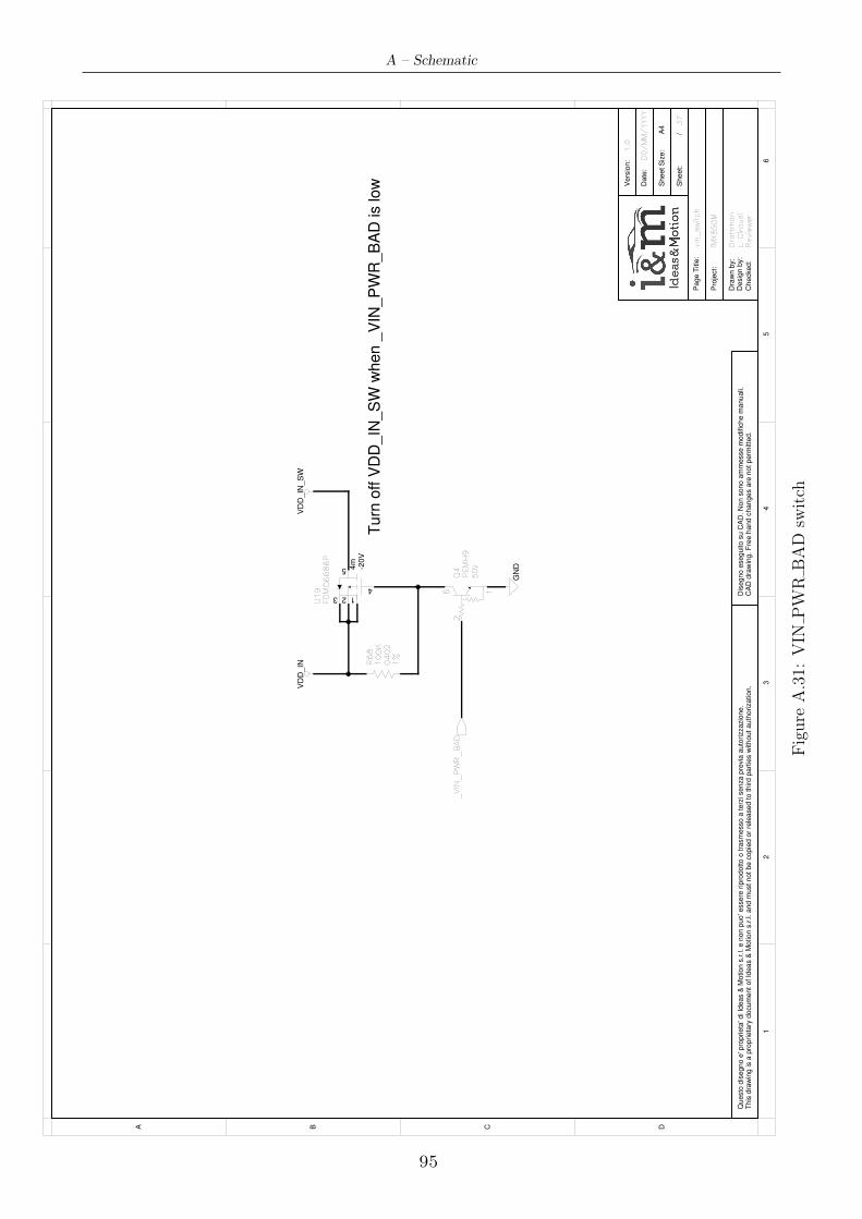
A – Schematic
R6
8
04
02
10
0K
1%
VD
D_IN
U1
9F
DM
C6
68
6P
4m
-20V
3
5
412
VD
D_IN
_S
W
_V
IN_
PW
R_
BA
DQ
4
16
2P
EM
H9
50
V
CA
D d
raw
ing. F
ree h
and c
hanges a
re n
ot perm
itte
d.
Dis
egno e
seguito s
u C
AD
. N
on s
ono a
mm
esse m
odific
he m
anuali.
This
dra
win
g is a
pro
prieta
ry d
ocum
ent of Id
eas &
Motion s
.r.l. and m
ust not be c
opie
d o
r re
leased to third p
art
ies w
ithout auth
orization.
Questo
dis
egno e
' pro
prieta
' di Id
eas &
Motion s
.r.l. e n
on p
uo' e
ssere
rip
rodotto o
tra
sm
esso a
terz
i senza p
revia
auto
rizzazio
ne.
Dra
wn b
y:
Checked:
Desig
n b
y:
Pro
ject:
Sheet S
ize:
Page T
itle
:
Sheet:
Date
:
Vers
ion:
/A4
A B C D
12
34
56
Re
vie
we
rL
. G
ira
ud
i
iMX
8S
OM
Dra
ftm
an
37
1.0
DD
/M
M/
YY
YY
vin
_s
wit
ch
GN
D
Turn
off V
DD
_IN
_S
W w
hen _
VIN
_P
WR
_B
AD
is low
Figure
A.31:
VIN
PW
RBAD
switch
95
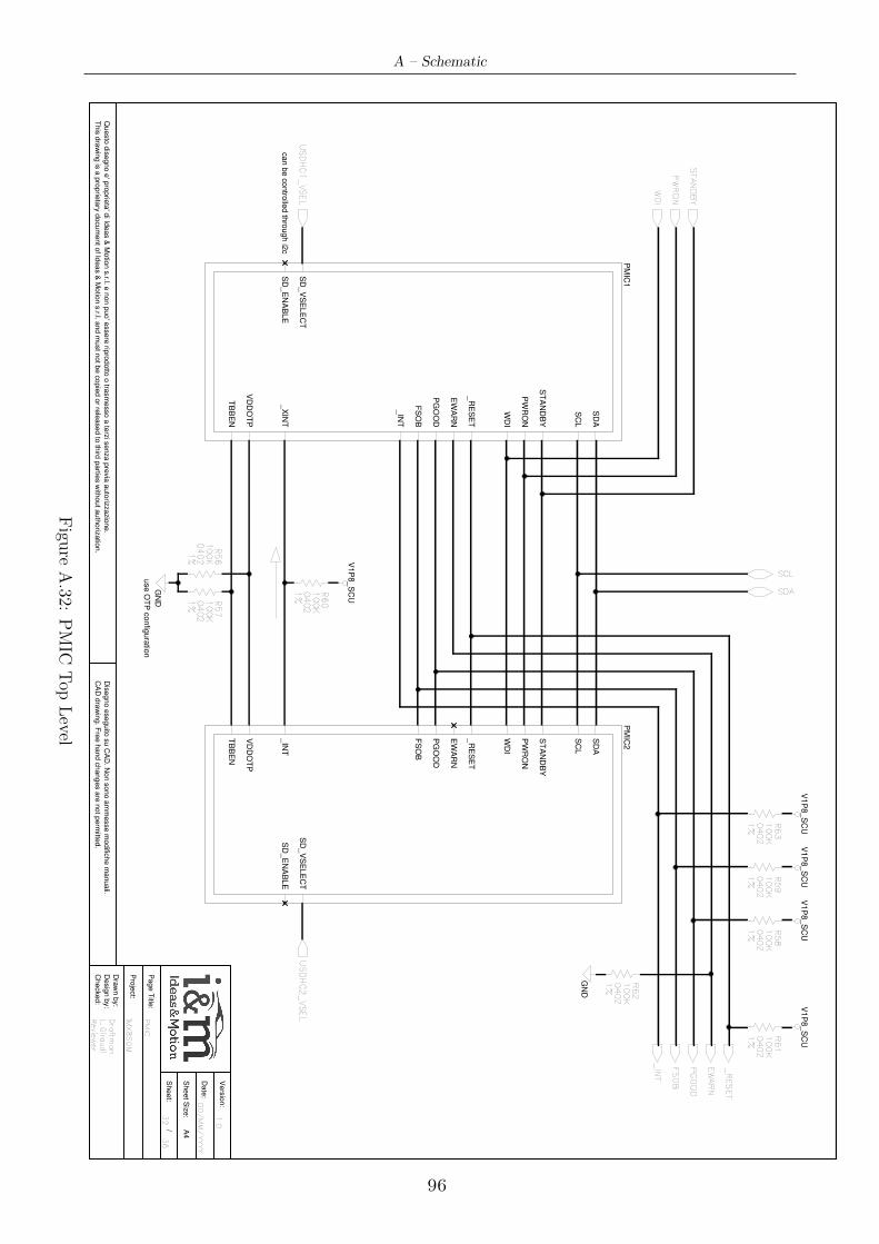
A – Schematic
Dra
wn b
y:
Checked:
Desig
n b
y:
Pro
ject:
Sheet S
ize:
Page T
itle:
Date
:
Vers
ion:
CA
D d
raw
ing. F
ree h
and c
hanges a
re n
ot p
erm
itted.
Dis
egno e
seguito
su C
AD
. Non s
ono a
mm
esse m
odific
he m
anuali.
This
dra
win
g is
a p
roprie
tary
docum
ent o
f Ideas &
Motio
n s
.r.l. and m
ust n
ot b
e c
opie
d o
r rele
ased to
third
partie
s w
ithout a
uth
oriz
atio
n.
Questo
dis
egno e
' pro
prie
ta' d
i Ideas &
Motio
n s
.r.l. e n
on p
uo' e
ssere
ripro
dotto
o tra
sm
esso a
terz
i senza p
revia
auto
rizzazio
ne.
Sheet:
/ A4
PM
IC
DD
/M
M/
YY
YY
1.0
36
32
L. G
irau
di
iMX
8S
OM
Dra
ftma
n
Re
vie
we
r
SCL
SDA
STA
ND
BY
PW
RO
N
SD
A
SC
L
ST
AN
DB
Y
PW
RO
N
WD
I
_R
ES
ET
EW
AR
N
_IN
T
_X
INT
VD
DO
TP
TB
BE
N
PG
OO
D
SD
_V
SE
LE
CT
SD
_E
NA
BLE
FS
OB
PM
IC1
SD
A
SC
L
ST
AN
DB
Y
PW
RO
N
WD
I
_R
ES
ET
EW
AR
N
_IN
T
VD
DO
TP
TB
BE
N
PG
OO
D
SD
_V
SE
LE
CT
SD
_E
NA
BLE
FS
OB
PM
IC2
_R
ES
ET
EW
AR
N
_IN
T
US
DH
C2
_V
SE
L
WD
I
PG
OO
D
GN
D
use O
TP
config
ura
tion
US
DH
C1
_V
SE
L
04
02
R5
6
1%
10
0K
04
02
R5
7
1%
10
0K
FS
OB
04
02
R5
81
00
K
1%
1%
10
0K
R5
9
04
02
V1P
8_S
CU
V1P
8_S
CU
04
02
R6
01
00
K
1%
V1P
8_S
CU
04
02
R6
11
00
K
1%
V1P
8_S
CU
04
02
R6
21
00
K
1%
GN
D
1%
10
0K
R6
3
04
02
V1P
8_S
CU
can b
e c
ontro
lled th
rough i2
c
Figu
reA.32:
PMIC
Top
Level
96
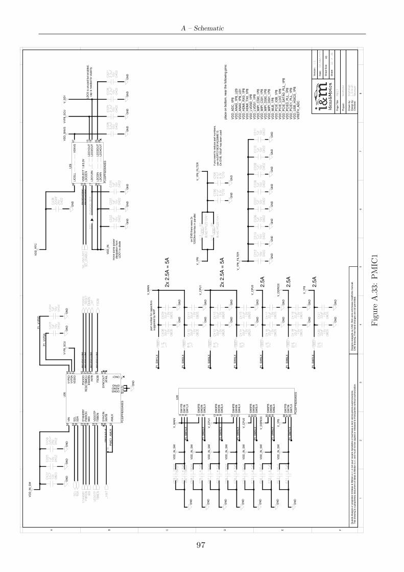
A – Schematic
SW
1F
BS
W1IN
SW
1LX
SW
2F
BS
W2IN
SW
2LX
SW
3F
BS
W3IN
SW
3LX
SW
4F
BS
W4IN
SW
4LX
SW
5F
BS
W5IN
SW
5LX
SW
6F
BS
W6IN
SW
6LX
SW
7F
BS
W7IN
SW
7LX
LD
O12IN
LIC
ELL
LD
O2E
N
LD
O4IN
LD
O3IN
VS
ELE
CT
LD
O1O
UT
LD
O3O
UT
LD
O2O
UT
LD
O4O
UT
VS
NV
S
1.8
/3.3
V
XF
AIL
V1P
5D
V1P
5A
SY
NC
OU
T
RE
SE
TB
MC
U
VD
DIO
EW
AR
N
FS
OB
INT
B
PG
OO
D
VD
DO
TP
VIN
SC
LS
DA
ST
AN
DB
Y
SY
NC
IN
AM
UX
TB
BE
N
WD
I
XIN
TB
PW
RO
N
DGNDAGND
DNC1
EPAD
GN
D
GN
DG
ND
GN
D
GN
DG
ND
GN
D
GN
D
GN
DG
ND
GN
DG
ND
GN
DG
ND
GN
DG
ND
GN
DG
ND
GN
DG
ND
3 4 5 2 7 6
13 8 9
12
11
10
31
32
33
30
35
34
38
37
36
PC
33P
F8200A
0E
S
U26
17
46
43
27
26
16
15
25
18
28
47
PC
33P
F8200A
0E
S
U26
44
40
41
49
21
54
20
29
24
42
53
50
55
56
23
48
52
14
19
39
22
4551
1
57
PC
33P
F8200A
0E
S
U26
VD
D_IN
_S
W
25
V2
20
nF
04
02
C4
38
10
V1
uF
04
02
C2
00
04
02
1u
F1
0V
C2
01
10
V1
uF
04
02
C2
02
04
02
1u
F1
0V
C2
03
10
V1
uF
04
02
C2
04
10
V2
2u
F
08
05
C4
08
VD
D_IN
04
02
2.2
uF
10
V
C3
25
10
V2
.2u
F
04
02
C3
26
V1P
8_S
CU
1uHL17
22
uF
08
05
10
V
C4
09
10
V2
2u
F
08
05
C4
10
1uHL18
08
05
22
uF
10
V
C4
11
V_M
AIN
4.7
uF
C7
1
C4
12
08
05
22
uF
10
V
1uHL19
10
V2
2u
F
08
05
C4
13
V_C
PU
1
C4
14
08
05
22
uF
10
V
1uHL20
10
V2
2u
F
08
05
C4
15
C4
16
08
05
22
uF
10
V
1uHL21
10
V2
2u
F
08
05
C4
17
VD
D_IN
_S
W
V_C
PU
0
PM
IC1_A
MU
X
P1_V
1P
5D
P1_V
1P
5A
P1_S
W1LX
P1_S
W1LX
P1_S
W2LX
P1_S
W2LX
P1_S
W3LX
P1_S
W4LX
P1_S
W5LX
P1_S
W6LX
P1_S
W7LX
P1_S
W3LX
P1_S
W4LX
P1_S
W5LX
Dra
wn b
y:
Checked:
Desig
n b
y:
Pro
ject:
Sheet S
ize:
Page T
itle
:
Sheet:
Date
:
Vers
ion:
CA
D d
raw
ing. F
ree h
and c
hanges a
re n
ot perm
itte
d.
Dis
egno e
seguito s
u C
AD
. N
on s
ono a
mm
esse m
odific
he m
anuali.
This
dra
win
g is a
pro
prieta
ry d
ocum
ent of Id
eas &
Motion s
.r.l. and m
ust not be c
opie
d o
r re
leased to third p
art
ies w
ithout auth
orization.
Questo
dis
egno e
' pro
prieta
' di Id
eas &
Motion s
.r.l. e n
on p
uo' e
ssere
rip
rodotto o
tra
sm
esso a
terz
i senza p
revia
auto
rizzazio
ne.
/A3
12
34
56
78
A B C D E F
Re
vie
we
r
Dra
ftm
an
iMX
8S
OM
L.
Gir
au
di
33
36
1.0
DD
/M
M/
YY
YY
PM
IC1
GN
DG
ND
C4
18
08
05
22
uF
10
V
L221uH
08
05
C4
19
10
V2
2u
F
V_D
DR
IO0
P1_S
W6LX
GN
DG
ND
C4
20
08
05
22
uF
10
V
L231uH
08
05
C4
21
10
V2
2u
F
V_1P
8
P1_S
W7LX
_R
ES
ET
_X
INT
TB
BE
NV
DD
OTP
VD
D_R
TC
VD
D_S
NV
SV
1P
8_S
CU
_IN
T
C2
05
04
02
1u
F1
0V
SD
AS
CL
STA
ND
BY
PW
RO
NW
DI
EW
AR
N
PG
OO
DS
D_
VS
ELE
CT
2.2
uF
10
V0
40
2
C3
27
GN
D
LD
O3 is u
nused b
ut enable
d,
cap is n
eeded for
sta
bili
ty
10
0n
FC
53
GN
D
GN
D
4.7
uF
C7
2
10
0n
FC
54
GN
D
4.7
uF
C7
3
10
0n
FC
55
GN
D
4.7
uF
C7
4
10
0n
FC
56
GN
D
4.7
uF
C7
5
10
0n
FC
57
GN
D
4.7
uF
C7
6
10
0n
FC
58
GN
D
4.7
uF
25
V0
60
3C
77
16
V1
00
nF
04
02
C5
9
move s
om
e p
ow
er
dis
sip
ation fro
mLD
O1 to d
iode o
n E
VB
there
were
2x
120O
hm
ferr
ites in p
ara
llel
C3
90
12
10
47
uF
6.3
V6
.3V
47
uF
12
10
C3
91
GN
DG
ND
pla
ce o
n b
ottom
, near
the follo
win
g p
ins:
VD
D_A
DC
_1P
8V
DD
_A
NA
0_1P
8_U
29
VD
D_A
NA
0_1P
8_U
31
VD
D_H
DM
I_R
X0_1P
8V
DD
_H
DM
I_T
X0_1P
8V
DD
_LV
DS
0_1P
8V
DD
_LV
DS
1_1P
8V
DD
_M
IPI_
CS
I0_1P
8V
DD
_M
IPI_
CS
I1_1P
8V
DD
_M
IPI_
DS
I0_1P
8V
DD
_M
IPI_
DS
I1_1P
8V
DD
_M
LB
_1P
8V
DD
_P
CIE
_IO
B_1P
8V
DD
_P
CIE
_LD
O_1P
8V
DD
_P
CIE
_S
AT
A0_P
LL_1P
8V
DD
_P
CIE
0_P
LL_1P
8V
DD
_P
CIE
1_P
LL_1P
8V
DD
_U
SB
_H
SIC
0_1P
8V
RE
FH
_A
DC
SD
_E
NA
BLE
FS
OB
open-d
rain
outp
ut
open-d
rain
outp
ut
open-d
rain
outp
ut
open-d
rain
outp
ut
inte
rnal pull-
up
GN
DG
ND
C4
22
08
05
22
uF
10
V
PN
S4
00
10
ER
2
DD
1
inte
rnal pull-
dow
n
inte
rnal pull-
dow
n
1
V_S
D1
C3
28
04
02
2.2
uF
10
V
GN
D
04
02
C4
39
25
V2
20
nF
V_M
AIN
V_C
PU
1
V_C
PU
0
V_D
DR
IO0
V_1P
8
L1
3 BLM
21
PG
22
1S
N1
0H
0H
L1
4 BLM
21
PG
22
1S
N1
V_1P
8
GN
DG
ND
GN
DG
ND
GN
DG
ND
GN
DG
ND
04
02
1u
F1
0V
C2
06
10
V1
uF
04
02
C2
07
C2
08
1u
F
04
02
10
V1
0V
1u
F
04
02
C2
09
04
02
1u
F1
0V
C2
10
1u
FC
21
1
10
V0
40
2
C2
12
04
02
1u
F1
0V
10
V1
uF
04
02
C2
13
V_1P
8_F
ILT
ER
V_1P
8_F
ILT
ER
part
num
ber
for
capacitors
suggeste
d b
y N
XP
if y
ou w
ant to
reduce p
art
num
bers
,use 4
xG
RT
21B
C81A
226M
E13.
On E
VB
, 100uF
has b
een u
sed
2x 2
.5A
= 5
A
2x 2
.5A
= 5
A
2.5
A
2.5
A
2.5
A
VD
D_IN
_S
W
VD
D_IN
_S
W
VD
D_IN
_S
W
VD
D_IN
_S
W
VD
D_IN
_S
W
VD
D_IN
_S
W
T8
Figure
A.33:
PMIC
1
97
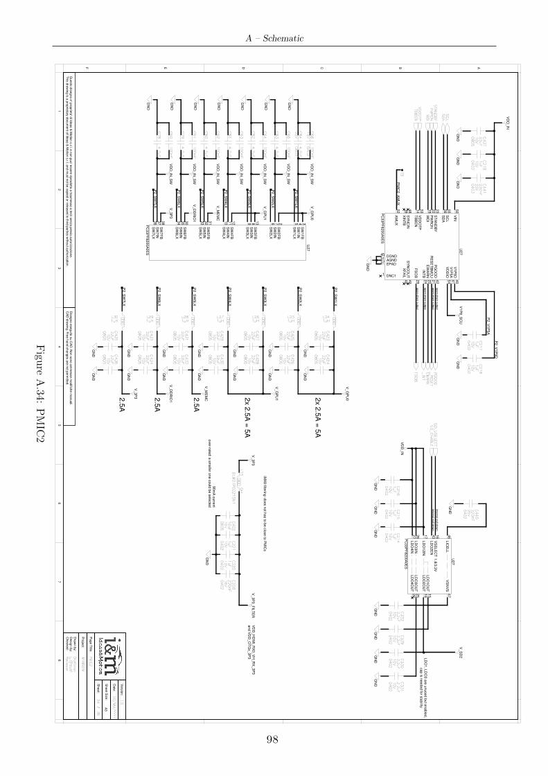
A – Schematic
Dra
wn b
y:
Checked:
Desig
n b
y:
Pro
ject:
Sheet S
ize:
Page T
itle:
Sheet:
Date
:
Vers
ion:
CA
D d
raw
ing. F
ree h
and c
hanges a
re n
ot p
erm
itted.
Dis
egno e
seguito
su C
AD
. Non s
ono a
mm
esse m
odific
he m
anuali.
This
dra
win
g is
a p
roprie
tary
docum
ent o
f Ideas &
Motio
n s
.r.l. and m
ust n
ot b
e c
opie
d o
r rele
ased to
third
partie
s w
ithout a
uth
oriz
atio
n.
Questo
dis
egno e
' pro
prie
ta' d
i Ideas &
Motio
n s
.r.l. e n
on p
uo' e
ssere
ripro
dotto
o tra
sm
esso a
terz
i senza p
revia
auto
rizzazio
ne.
/ A3
12
34
56
78
ABCDEF
Re
vie
we
r
Dra
ftma
n
iMX
8S
OM
L. G
irau
di
34
36
1.0
DD
/M
M/
YY
YY
PM
IC2
SW
1F
BS
W1IN
SW
1LX
SW
2F
BS
W2IN
SW
2LX
SW
3F
BS
W3IN
SW
3LX
SW
4F
BS
W4IN
SW
4LX
SW
5F
BS
W5IN
SW
5LX
SW
6F
BS
W6IN
SW
6LX
SW
7F
BS
W7IN
SW
7LX
XF
AIL
V1P
5D
V1P
5A
SY
NC
OU
T
RE
SE
TB
MC
U
VD
DIO
EW
AR
N
FS
OB
INT
B
PG
OO
D
VD
DO
TP
VIN
SC
LS
DA
ST
AN
DB
Y
SY
NC
IN
AM
UX
TB
BE
N
WD
I
XIN
TB
PW
RO
N
DGNDAGND
DNC1
EPAD
GN
D
GN
DG
ND
GN
D
GN
DG
ND
GN
D
GN
D
GN
DG
ND
GN
DG
ND
GN
DG
ND
GN
DG
ND
GN
DG
ND
GN
DG
ND
GN
DG
ND
GN
DG
ND
GN
D
GN
D
GN
D
GN
D
GN
D
GN
D
GN
D
GN
D
GN
DG
ND
GN
D
LD
O1, L
DO
3 a
re u
nused b
ut e
nable
d,
cap is
needed fo
r sta
bility
open-d
rain
outp
ut
open-d
rain
outp
ut
open-d
rain
outp
ut
open-d
rain
outp
ut
inte
rnal p
ull-d
ow
n
inte
rnal p
ull-d
ow
n
VD
D_IN
VD
D_IN
V1P
8_S
CU
V_S
D2
PM
IC2_A
MU
X
P2_V
1P
5D
P2_V
1P
5A
P2_S
W1LX
P2_S
W1LX
P2_S
W2LX
P2_S
W2LX
P2_S
W3LX
P2_S
W4LX
P2_S
W5LX
P2_S
W6LX
P2_S
W7LX
P2_S
W3LX
P2_S
W4LX
P2_S
W5LX
P2_S
W6LX
P2_S
W7LX
_R
ES
ET
TB
BE
NV
DD
OTP
_IN
T
SD
AS
CL
STA
ND
BY
PW
RO
NW
DI
EW
AR
N
PG
OO
DS
D_
VS
ELE
CT
SD
_E
NA
BLE
FS
OB
V_G
PU
0
V_G
PU
1
V_M
EM
C
V_D
DR
IO1
V_3P
3
V_G
PU
0
V_G
PU
1
V_M
EM
C
V_D
DR
IO1
V_3P
3
C8
14
.7u
F
C6
21
00
nF
C8
04
.7u
F
C6
11
00
nF
C7
94
.7u
F
C6
01
00
nF
C3
31
04
02
10
V2
.2u
F
10
V1
uF
04
02
C2
19
22
uF
10
V
C4
36
08
05
10
V2
2u
F
08
05
C4
35
22
uF
10
V
C4
34
08
05
10
V2
2u
F
08
05
C4
33
C4
28
08
05
22
uF
10
V
10
V2
2u
F
08
05
C4
29
C4
32
08
05
22
uF
10
V
C4
30
08
05
22
uF
10
V
10
V2
2u
F
08
05
C4
31
10
V2
2u
F
08
05
C4
27
C7
84
.7u
F
C4
26
10
V2
2u
F
08
05
C4
25
08
05
22
uF
10
V
C4
24
10
V0
80
5
22
uF
C3
30
04
02
2.2
uF
10
V
C3
29
10
V2
.2u
F
04
02
C4
23
08
05
22
uF
10
V
C2
18
10
V1
uF
04
02
C2
17
10
V1
uF
04
02
C2
16
10
V1
uF
04
02
C2
15
10
V1
uF
04
02
C2
14
10
V1
uF
04
02
C4
40
04
02
22
0n
F2
5V
U27
PC
33P
F8200A
0E
S
57
1
5145
22
39
19
14
52
48
23
56
55
50
53
42
24
29
20
54
21
49
41
40
44
U27
PC
33P
F8200A
0E
S
36
37
38
34
35
30
33
32
31
10
11
12 9 8
13 6 7 2 5 4 3
22
0n
F2
5V
C4
41
04
02
10
V2
.2u
F
04
02
C3
32
10
V2
2u
F
08
05
C4
37
C6
60
40
21
00
nF
16
V
C8
40
60
32
5V
4.7
uF
C6
51
00
nF
C8
34
.7u
F
C6
41
00
nF
C8
24
.7u
F
C6
31
00
nF
2x 2
.5A
= 5
A
2x 2
.5A
= 5
A
2.5
A
2.5
A
2.5
A
VD
D_IN
_S
W
VD
D_IN
_S
W
VD
D_IN
_S
W
VD
D_IN
_S
W
VD
D_IN
_S
W
VD
D_IN
_S
W
VD
D_IN
_S
W
GN
D
90m
A c
urre
nt
over-ra
ted: a
sm
alle
r one c
ould
be s
ele
cte
d
VD
D_H
DM
I_R
X0_V
H_R
X_3P
3and V
DD
_O
TG
x_3P
3V
_3P
3
0H
BLM
21
PG
22
1S
N1
L1
5
16
V2
20
nF
04
02
C3
09
V_3P
3_F
ILT
ER
C2
20
04
02
1u
F1
0V
10
V1
uF
04
02
C2
21
C4
02
08
05
10
uF
10
V
LD
O12IN
LIC
ELL
LD
O2E
N
LD
O4IN
LD
O3IN
VS
ELE
CT
LD
O1O
UT
LD
O3O
UT
LD
O2O
UT
LD
O4O
UT
VS
NV
S
1.8
/3.3
V
17
46
43
27
26
16
15
25
18
28
47
PC
33P
F8200A
0E
S
U27
T9
L241uH1uH
L25L261uH1uH
L27L281uH1uH
L29L301uH
iMX
8 filte
ring: d
oes n
ot h
as to
be c
lose to
PM
ICs
Figu
reA.34:
PMIC
2
98
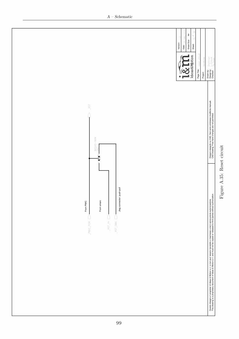
A – Schematic
Dra
wn b
y:
Checked:
Desig
n b
y:
Pro
ject:
Sheet S
ize:
Page T
itle
:
Date
:
Vers
ion:
CA
D d
raw
ing. F
ree h
and c
hanges a
re n
ot perm
itte
d.
Dis
egno e
seguito s
u C
AD
. N
on s
ono a
mm
esse m
odific
he m
anuali.
This
dra
win
g is a
pro
prieta
ry d
ocum
ent of Id
eas &
Motion s
.r.l. and m
ust not be c
opie
d o
r re
leased to third p
art
ies w
ithout auth
orization.
Questo
dis
egno e
' pro
prieta
' di Id
eas &
Motion s
.r.l. e n
on p
uo' e
ssere
rip
rodotto o
tra
sm
esso a
terz
i senza p
revia
auto
rizzazio
ne.
Sheet:
/A4
Jta
g c
onnecto
r: p
ush-p
ull
_R
ST_
IN
_R
ST_
DB
G
res
et_
cir
cu
it
L.
Gir
au
di
Re
vie
we
r
Dra
ftm
an
DD
/M
M/
YY
YY
iMX
8S
OM
36
35
1.0
_P
MIC
_P
OR
_R
ST
DS
7
3
1
2
BA
S4
0-
06
W
Fro
m s
marc
Fro
m P
MIC
Figure
A.35:
Reset
circuit
99
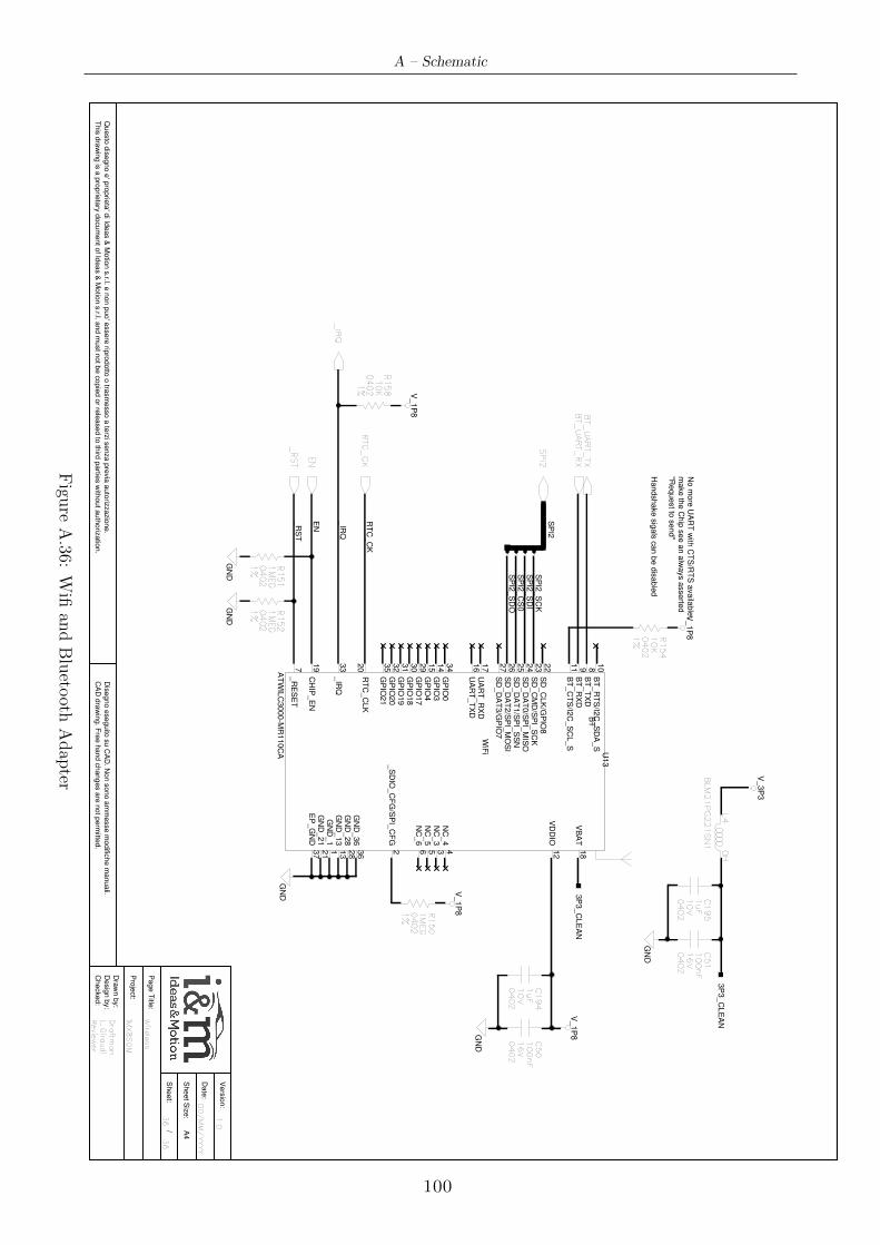
A – Schematic
Dra
wn b
y:
Checked:
Desig
n b
y:
Pro
ject:
Sheet S
ize:
Page T
itle:
Date
:
Vers
ion:
CA
D d
raw
ing. F
ree h
and c
hanges a
re n
ot p
erm
itted.
Dis
egno e
seguito
su C
AD
. Non s
ono a
mm
esse m
odific
he m
anuali.
This
dra
win
g is
a p
roprie
tary
docum
ent o
f Ideas &
Motio
n s
.r.l. and m
ust n
ot b
e c
opie
d o
r rele
ased to
third
partie
s w
ithout a
uth
oriz
atio
n.
Questo
dis
egno e
' pro
prie
ta' d
i Ideas &
Motio
n s
.r.l. e n
on p
uo' e
ssere
ripro
dotto
o tra
sm
esso a
terz
i senza p
revia
auto
rizzazio
ne.
Sheet:
/ A4
iMX
8S
OM
Dra
ftma
n
Re
vie
we
r
L. G
irau
di
Wire
les
s
DD
/M
M/
YY
YY
1.0
36
36
NC
_4
NC
_3
NC
_5
NC
_6
VB
AT
RT
C_C
LK
BT
_C
TS
/I2C
_S
CL_S
BT
_R
TS
/I2C
_S
DA
_S
BT
_R
XD
BT
_T
XD
_R
ES
ET
SD
_C
LK
/GP
IO8
SD
_C
MD
/SP
I_S
CK
SD
_D
AT
0/S
PI_
MIS
OS
D_D
AT
1/S
PI_
SS
NS
D_D
AT
2/S
PI_
MO
SI
SD
_D
AT
3/G
PIO
7
EP
_G
ND
GN
D_36
GN
D_28
GN
D_13
GN
D_1
GN
D_21
CH
IP_E
N
UA
RT
_R
XD
UA
RT
_T
XD
VD
DIO
_S
DIO
_C
FG
/SP
I_C
FG
GP
IO0
GP
IO3
GP
IO4
GP
IO17
GP
IO18
GP
IO19
GP
IO20
GP
IO21
_IR
Q
WiF
i
BT
33
35
32
31
30
29
15
14
34
2 12
16
17
19
21
1 13
28
36
37
27
26
25
24
23
227 89
10
11
20
18
6 5 3 4
AT
WIL
C3000-M
R110C
AG
ND
R1
50
04
02
1M
EG
1%
V_1P
8
C1
94
04
02
1u
F1
0V
C5
0
04
02
10
0n
F1
6V
GN
D
V_1P
8
3P
3_C
LE
AN
3P
3_C
LE
AN
V_3P
3
L4
BLM
21
PG
22
1S
N1
0H
GN
D
C1
95
04
02
1u
F1
0V
C5
1
04
02
10
0n
F1
6V
RTC
_C
K
_IR
Q
_R
ST
EN
BT_
UA
RT_
TX
BT_
UA
RT_
RX
SP
I2
RT
C_C
K
_IR
Q
_R
ST
EN
SP
I2
SP
I2_C
S0
SP
I2_S
CK
SP
I2_S
DI
SP
I2_S
DO
V_1P
8N
o m
ore
UA
RT
with
CT
S/R
TS
availa
ble
:m
ake th
e C
hip
see a
n a
lways a
sserte
d"R
equest to
send"
V_1P
8
R1
51
04
02
1M
EG
1%
1%
1M
EG
04
02
R1
52
GN
DG
ND
U13
Handshake s
igals
can b
e d
isable
d
R1
54
04
02
10
K
1%
1%
10
K0
40
2
R1
58
Figu
reA.36:
Wifi
andBlueto
othAdap
ter
100
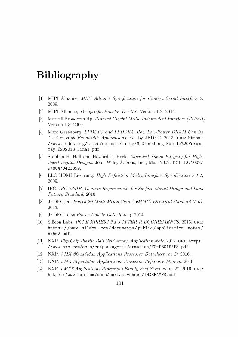
Bibliography
[1] MIPI Alliance. MIPI Alliance Specification for Camera Serial Interface 2.2009.
[2] MIPI Alliance, ed. Specification for D-PHY. Version 1.2. 2014.
[3] Marvell Broadcom Hp. Reduced Gigabit Media Independent Interface (RGMII).Version 1.3. 2000.
[4] Marc Greenberg. LPDDR3 and LPDDR4: How Low-Power DRAM Can BeUsed in High Bandwidth Applications. Ed. by JEDEC. 2013. url: https://www.jedec.org/sites/default/files/M_Greenberg_Mobile%20Forum_
May_%202013_Final.pdf.
[5] Stephen H. Hall and Howard L. Heck. Advanced Signal Integrity for High-Speed Digital Designs. John Wiley & Sons, Inc., Mar. 2009. doi: 10.1002/9780470423899.
[6] LLC HDMI Licensing. High Definition Media Interface Specification v 1.4.2009.
[7] IPC. IPC-7351B. Generic Requirements for Surface Mount Design and LandPattern Standard. 2010.
[8] JEDEC, ed. Embedded Multi-Media Card (e•MMC) Electrical Standard (5.0).2013.
[9] JEDEC. Low Power Double Data Rate 4. 2014.
[10] Silicon Labs. PCI E XPRESS 3.1 J ITTER R EQUIREMENTS. 2015. url:https://www.silabs.com/documents/public/application- notes/
AN562.pdf.
[11] NXP. Flip Chip Plastic Ball Grid Array, Application Note. 2012. url: https://www.nxp.com/docs/en/package-information/FC-PBGAPRES.pdf.
[12] NXP. i.MX 8QuadMax Applications Processor Datasheet rev D. 2016.
[13] NXP. i.MX 8QuadMax Applications Processor Reference Manual. 2016.
[14] NXP. i.MX8 Applications Processors Family Fact Sheet. Sept. 27, 2016. url:https://www.nxp.com/docs/en/fact-sheet/IMX8FAMFS.pdf.
101
BIBLIOGRAPHY
[15] NXP. Level shifting techniques in I2C-bus design. 2007.
[16] NXP. PF8x00 Datasheet Rev. 2.0. 2018.
[17] PCI-SIG. PCI Express Base Specification Revision 3.0. 2010.
[18] Donovan Porter. 100BASE-T1 Ethernet: the evolution of automotive net-working. Ed. by Texas Instrument. 2018.
[19] SAE. J3016: Taxonomy and Definitions for Terms Related to Driving Au-tomation Systems for On-Road Motor Vehicles. 2014.
[20] NXP Semiconductor. MIPI–CSI2 Peripheral on i.MX6 MPUs. 2016.
[21] ON Semiconductor. A System Designer’s Guide for Building a PCIe ® ClockTree while Addressing Timing Challenges. 2015. url: http://www.onsemi.com/pub/Collateral/AND9202-D.PDF.
[22] SGET. Smart Mobility ARChitecture, Design Guide. SMARC Design Guide2.0. Mar. 23, 2017. url: https://www.sget.org/standards/smarc.html.
[23] SGET. Smart Mobility ARChitecture, Hardware Specification. Version 2.0.June 2, 2016. url: https://www.sget.org/fileadmin/user_upload/SMARC_Hardware_Specification_V200_Errata.zip.
[24] USB-IF. Universal Serial Bus Specification. Version 2.0. 2000.
102