Embed Size (px)
Citation preview
Development of Crystalline Germanium for Thermophotovoltaics and
High-Efficiency Multi-Junction Solar Cells
Dissertation
zur Erlangung des akademischen Grades des Doktor der Naturwissenschaften (Dr. rer. nat.)
an der Universität Konstanz Fakultät für Physik
vorgelegt von
Jara Fernández
Fraunhofer Institut für Solare Energiesysteme
Freiburg
2010
Dissertation der Universität KonstanzTag der mündlichen Prüfung: 29.04.2011
Referent: Prof. Dr. Gerhard WillekeReferent: Prof. Dr. Thomas Dekorsy
iii
Acknowledgements
Working as a PhD student at Fraunhofer ISE in Freiburg was a very rewarding and challenging experience for me. During all these years, many people have supported me in this endeavour. I can hardly imagine the success of this work without these people. Here is a small tribute to all them: First of all, I want to thank Prof. Gerhard Willeke for accepting me as one of his students, for his valuable advice and inspiring discussions, for his patience in the proofreading and for the support and encouragement during the last months. Prof. Thomas Dekorsy and Prof. Peter Nielaba from the Universty of Konstanz were also mem-bers of my supervisory panel, for which I am grateful. I want to thank Dr. Andreas Bett and Dr. Frank Dimroth for offering me valuable advice and for allowing me great freedom in my research. I am grateful to Dr. Stefan Glunz and Dr. Stefan Rein for answering many questions about silicon and characterization measurements. My special thanks go out to Dominic Suwito, who supported me in the passivation technology, characterization, mathematical simulation and for sharing with me a fascination for germanium. I also take this opportunity to express my special gratitude toward Dr. Eduard Oliva for explaining to me all about solar cell technology. It was a pleasure to work with the III-V technology group. I would especially like to thank Elvira Fehrenbacher, Rüdiger Löckenhof, Swita Wassie and Ranka Koch for their crucial support in cell technology and the great and motivating work atmosphere. I am grateful to Elke Wesler and Rene Kellenbenz for the growth of the cells, Benjamin George for his absorption measurements and Martin Hermle and Simon Philipps for their help in the simulations. I want also to thank Dr Marc Hoffman and Dr Stefan Janz, who helped me with the plasma technology, Dr.Thomas Roth, Dr.Stefan Diez and Phillip Rosenits for the characterization support and Jan Nekarda for the laser fired contacts. I want to thank Raymond Hoheisel, Gerald Siefer, Elisabeth Schäffer, Tobias Gandy and Michael Schachtner for the solar cells measure-ments, Luciana Meinking and Wesley Dopkins for the proofreading and Gerald Siefer and Ray-mond Hoheisel for the German proofreading. I am also grateful to Alejandro Datas from the Instituto de Energia Solar in Madrid for the co-working and for answering the many questions about the TPV system. I would like to thank my workmates for creating a very good atmosphere: Daniel Stetter, Marc Steiner, Tobias Rösener, Henning Helmers, Fabian Eltermann and Johannes Schubert. My DAAD friends in Freiburg; Agnès Millet, Carlo Catoni, Katerina Marcekova, Almir Maljevic, Tamirace Fakhoury, Roza Umarova, and Anna Novokhatko for their friendship and support. My friends in Spain; Laura Alcober, Ana Bribián, Edurne Gállego, Javier Hernández, Clara Pau-les, Marta Villegas and Coral Merchán for always being there and for believing in me. Lucía Alvarez, Guadalupe Asensio, Maria Alba, Juan Miguel del Río, Isabel Fernández, Juan Pablo Ferrer, Michael Schossow, Teresa Orellana, Mark Schumann, Laura Serrano and Alberto Soria for the great moments we shared in Freiburg, for supporting me and believing in me. Finally, I wish to thank my parents and my sister Marta for their constant support and encourage-ment. Freiburg, October 2010

iv
v
Table of contents
Acknowledgments iii
1 Introduction 1 1.1 Motivation 1 1.2 Thesis outline 5
2 Germanium (Ge) 7 2.1 Introduction 7 2.2 Basics of Ge 9
2.2.1 Supply and crystal growth 9 2.2.2 Band structure 10
2.3 Optical properties 11 2.3.1 Electron-hole absorption 11 2.3.2 Free-carrier absorption and related phenomena 12
2.4 Electrical properties 14 2.4.1 Efective mass 14 2.4.2 Carrier densities 15 2.4.3 Conductivity and mobility 17
2.5 Theory of carrier lifetime 20 2.5.1 Generation and recombination 20 2.5.2 Carrier recombination mechanism 21 2.5.3 Effective lifetime and separation of bulk lifetime 26
3 Lifetime measurements 29 3.1 Introduction 29 3.2 Microwave-detected photoconductance decay technique 29
3.2.1 Measurement principle 29 3.2.2 Transient decay study of minority carrier lifetime in Ge 31 3.2.3 Differential and absolute lifetime 40
4 Ge surface passivation 43 4.1 Introduction 43
4.1.1 Fundamentals of surface passivation 43 4.1.2 State of the art passivation layers for Ge surfaces 45
4.2 Plasma enhanced chemical vapour deposition (PECVD) 46 4.2.1 Basics of plasma and plasma excitation 46 4.2.2 PECVD with the STS and SI reactors 49 4.2.3 PECVD with the AK400 reactor 50
vi
4.3 Optimization of Ge surface passivation using amorphous silicon and silicon nitride STS/SI 51 4.3.1 Wet chemical etching 51 4.3.2 Plasma cleaning 52 4.3.3 Plasma deposition of amorphous silicon and silicon nitride 54
4.4 Optimization of Ge surface passivation using amorphous silicon carbide AK400 54 4.4.1 Plasma cleaning 54 4.4.2 Plasma deposition of amorphous silicon carbide 55
4.5 Passivation mechanisms 57 4.5.1 Comparison between the passivation layers and the influence of annealing on p-Ge 57 4.5.2 Comparison between the passivation layers and the influence of annealing on i-Ge 59
4.6 Characterization of passivation layers 61 4.6.1 Effective lifetime and separation of bulk lifetime 61 4.6.2 Surface recombination velocity 64
4.7 Impact of intrinsic limits 65 4.8 Diffusion length in p-Ge 68
5 Ge thermophotovoltaic (TPV) cells 71 5.1 Introduction 71 5.2 Solar TPV system 72 5.3 Principles of Ge TPV cell 75 5.4 Development of back side technology 78 5.5 One-dimensional simulations using PC1D 81
5.5.1 Optical parameters 81 5.5.2 Analysis of the infrared mirror 86 5.5.3 Electrical parameters 89 5.5.4 Electrical passivation of Ge TPV cells 91
5.6 Effect of the back side passivation 94 5.7 Ge cells under TPV condition 96
6 Ge substrate optimization in triple-junction solar cells under space conditions 101 6.1 Introduction 101 6.2 Back side technology optimization 102 6.3 Optimal parameters for space conditions 103
6.3.1 Ideal case 104 6.3.2 Analysis of the cell parameters using PC1D 106
vii
6.4 Results and discussion 111 6.4.1 Passivation layer 111 6.4.2 Infrared mirror 114
7 Summary and outlook 117
8 Deutsche Zusammenfassung 121
9 Appendix: Characterization methods 125 9.1 Reflectometry 125 9.2 Quantum efficiency measurements 126 9.3 IV Measurements. MuSim set up 127
10 List of symbols, acronyms and constants 129
11 List of publications 133
12 Bibliographie 135

viii
Introduction
1
1 Introduction
This work explores the potential of germanium single-junction solar cells for
thermophotovoltaic (TPV) application and the potential of germanium bottom
cells for high-efficiency triple-junction solar cells. This chapter encourages the
necessity of studying the germanium material and provides the outline of the
thesis.
1.1 Motivation
The generation of electricity by means of the photovoltaic effect is one of the most promising methods to generate clean and renewable energy [1]. Most research in this field focuses on reducing the cost of photovoltaic energy generation in order to make this technique more at-tractive for the commercial market. Two main strategies can be followed in order to fulfill this requirement. The first strategy is to reduce the cost of the solar cell and module without losing too much of their efficiency. This can be obtained by using cheap substrates. The mainstream material used in the industry is multicrystalline silicon. Another possibility is to use thinner silicon substrates or other material systems like amorphous silicon, CdTe, CIGS or even or-ganic materials. The second strategy is to increase the solar cell conversion efficiency without increasing the cost too much. The research described in this thesis corresponds to this second method.
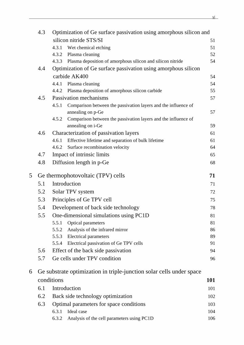
Several research groups focus on obtaining high conversion efficiency using high quality monocrystalline silicon. A remarkable achievement was obtained by means of a sophisticated technology [2]. However, single silicon solar cells absorb only a limited part of the sun spec-trum. The energy of photons with high energy is partly lost due to thermalization, whereas photons with low energy are not absorbed at all. The solar spectrum can be more profitably exploited using multiple stacking of solar cells with increasing band gap energies. This struc-ture reduces the transmission and thermalization losses using a low band gap bottom solar cell and a high band gap top solar cell, respectively (see Figure 1-1).
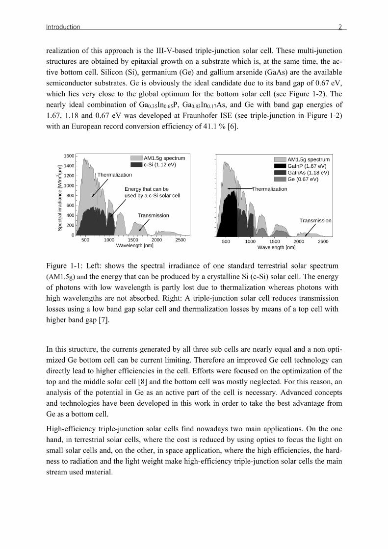
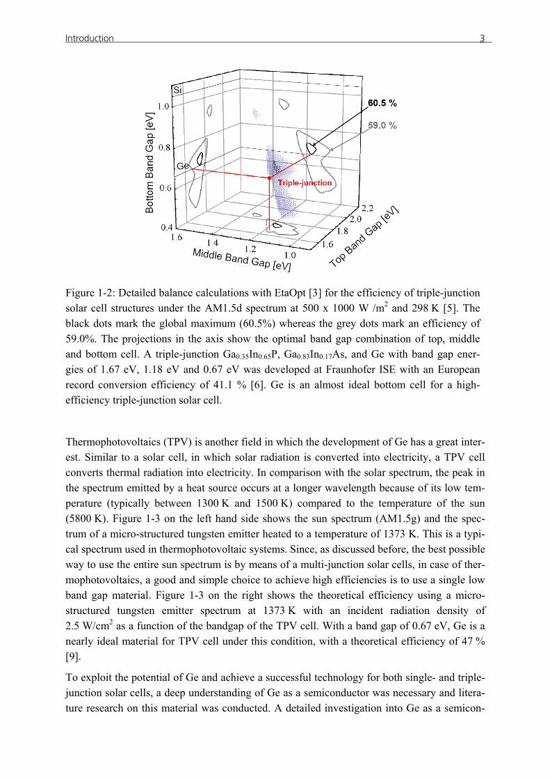
To find the most suitable combination of triple-junction solar cells which makes the best use of the solar spectrum, a simulation using EtaOpt was carried out. This program, developed at Fraunhofer ISE [3], uses the detailed balance method, first introduced by Shockley and Queis-ser [4], to evaluate the theoretical efficiencies of different solar cells design. Figure 1-2 shows how the conversion efficiency of a triple-junction solar cell varies with the band gap energies of the three individual junctions [5]. The global maximum (efficiency higher than 60.5 %) under AM1.5d spectrum at 500 x 1000 W /m2 and 298 K is represented in Figure 1-2 with black dots whereas the grey dots mark efficiencies of 59.0%. The three black areas in the axis of Figure 1-2 are the projections of the black dots and correspond to the optimum bandgaps of the top, middle and bottom cell. The maximum efficiency lies at a band gap combination of 1.74 eV, 1.17 eV and 0.70 eV, respectively. The currently most promising material for the
Introduction
2
realization of this approach is the III-V-based triple-junction solar cell. These multi-junction structures are obtained by epitaxial growth on a substrate which is, at the same time, the ac-tive bottom cell. Silicon (Si), germanium (Ge) and gallium arsenide (GaAs) are the available semiconductor substrates. Ge is obviously the ideal candidate due to its band gap of 0.67 eV, which lies very close to the global optimum for the bottom solar cell (see Figure 1-2). The nearly ideal combination of Ga0.35In0.65P, Ga0.83In0.17As, and Ge with band gap energies of 1.67, 1.18 and 0.67 eV was developed at Fraunhofer ISE (see triple-junction in Figure 1-2) with an European record conversion efficiency of 41.1 % [6].
500 1000 1500 2000 25000
200
400
600
800
1000
1200
1400
1600
Thermalization
Transmission
Energy that can be used by a c-Si solar cell
Spe
ctra
l irra
dian
ce [W
/m2 /µ
m]
AM1.5g spectrum c-Si (1.12 eV)
Wavelength [nm] 500 1000 1500 2000 2500
Transmission
Thermalization
AM1.5g spectrum GaInP (1.67 eV) GaInAs (1.18 eV) Ge (0.67 eV)
Wavelength [nm]
Figure 1-1: Left: shows the spectral irradiance of one standard terrestrial solar spectrum (AM1.5g) and the energy that can be produced by a crystalline Si (c-Si) solar cell. The energy of photons with low wavelength is partly lost due to thermalization whereas photons with high wavelengths are not absorbed. Right: A triple-junction solar cell reduces transmission losses using a low band gap solar cell and thermalization losses by means of a top cell with higher band gap [7].
In this structure, the currents generated by all three sub cells are nearly equal and a non opti-mized Ge bottom cell can be current limiting. Therefore an improved Ge cell technology can directly lead to higher efficiencies in the cell. Efforts were focused on the optimization of the top and the middle solar cell [8] and the bottom cell was mostly neglected. For this reason, an analysis of the potential in Ge as an active part of the cell is necessary. Advanced concepts and technologies have been developed in this work in order to take the best advantage from Ge as a bottom cell.
High-efficiency triple-junction solar cells find nowadays two main applications. On the one hand, in terrestrial solar cells, where the cost is reduced by using optics to focus the light on small solar cells and, on the other, in space application, where the high efficiencies, the hard-ness to radiation and the light weight make high-efficiency triple-junction solar cells the main stream used material.
Introduction
3
Figure 1-2: Detailed balance calculations with EtaOpt [3] for the efficiency of triple-junction solar cell structures under the AM1.5d spectrum at 500 x 1000 W /m2 and 298 K [5]. The black dots mark the global maximum (60.5%) whereas the grey dots mark an efficiency of 59.0%. The projections in the axis show the optimal band gap combination of top, middle and bottom cell. A triple-junction Ga0.35In0.65P, Ga0.83In0.17As, and Ge with band gap ener-gies of 1.67 eV, 1.18 eV and 0.67 eV was developed at Fraunhofer ISE with an European record conversion efficiency of 41.1 % [6]. Ge is an almost ideal bottom cell for a high-efficiency triple-junction solar cell.
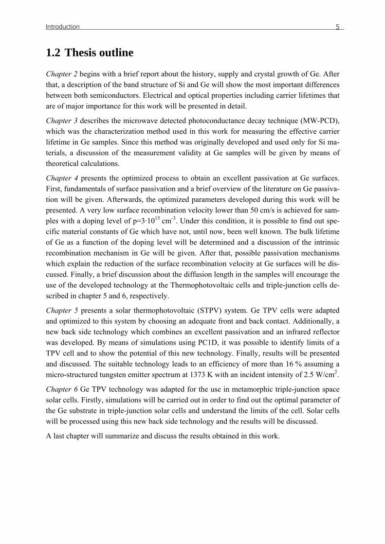
Thermophotovoltaics (TPV) is another field in which the development of Ge has a great inter-est. Similar to a solar cell, in which solar radiation is converted into electricity, a TPV cell converts thermal radiation into electricity. In comparison with the solar spectrum, the peak in the spectrum emitted by a heat source occurs at a longer wavelength because of its low tem-perature (typically between 1300 K and 1500 K) compared to the temperature of the sun (5800 K). Figure 1-3 on the left hand side shows the sun spectrum (AM1.5g) and the spec-trum of a micro-structured tungsten emitter heated to a temperature of 1373 K. This is a typi-cal spectrum used in thermophotovoltaic systems. Since, as discussed before, the best possible way to use the entire sun spectrum is by means of a multi-junction solar cells, in case of ther-mophotovoltaics, a good and simple choice to achieve high efficiencies is to use a single low band gap material. Figure 1-3 on the right shows the theoretical efficiency using a micro-structured tungsten emitter spectrum at 1373 K with an incident radiation density of 2.5 W/cm2 as a function of the bandgap of the TPV cell. With a band gap of 0.67 eV, Ge is a nearly ideal material for TPV cell under this condition, with a theoretical efficiency of 47 % [9].
To exploit the potential of Ge and achieve a successful technology for both single- and triple- junction solar cells, a deep understanding of Ge as a semiconductor was necessary and litera-ture research on this material was conducted. A detailed investigation into Ge as a semicon-
Introduction
4
ductor was carried out in the 1950s and 1960s and basic Ge properties like band structure and mobility are well known [10], [11]. However, since Si has gained in importance in microelec-tronics over recent years and, especially, after the 1960s, fewer studies on Ge have been un-dertaken and consequently many of the properties are not well-known. Besides, photovoltaic is a field where Ge has not been studied in depth and therefore important properties for the solar cells like, recombination mechanisms, bulk lifetimes and optical losses are not found in the literature and therefore have been thoroughly analysed in this work in order to understand and model the properties of Ge solar cells. A better understanding of Ge due to the determina-tion of these properties led to the identification of the optimal parameter for the processing of the solar cells, like substrate doping and thickness.
500 1000 1500 20000
200
400
600
800
1000
1200
1400
1600
Germaniumbottom cell
AM1.5g Structured tungsten spectrum at T=1373 K normalized to 1000 W/m2
Spec
tral i
rradi
ance
[W/m
2 /µm
]
Wavelength [nm]
Eg, Ge
Germaniumsingle TPV cell
0.0 0.2 0.4 0.6 0.8 1.0 1.20
10
20
30
40
50
Structured tungsten spectrum at T=1373 K, Intensity=2.5 W/cm2
Theo
retic
al e
ffici
ency
[%]
Bandgap energy [eV]
Eg,Ge=0,67 eV
Figure 1-3: Left: The AM1.5g spectrum [12] has a peak at 500 nm. In a metamorphic triple-junction solar cell the bottom cell absorbs energy in the range of (1050 nm>λ >1850 nm). The spectrum used in a TPV system [13] with a peak at 1500 nm is exploited more profita-bly using a single TPV solar cell with low bandgap semiconductor like Ge. Right: The theo-retical efficiency of a TPV cell as a function of the bandgap of the cell assuming a micro-structured tungsten emitter spectrum at 1373 K. Ge is a nearly ideal material for a TPV cell under this condition with a theoretical cell efficiency of about 47% [9].
Surface passivation technologies on Ge were also not deeply investigated in the past and are necessary to achieve the maximum potential of the Ge cell; therefore a new technology which incorporates a back surface passivation on Ge was developed and optimized in this work. For this purpose, well known Si technologies for photovoltaic applications were taken into con-sideration and were adapted to be used in Ge single-junction solar cells and triple-junction solar cells.
Introduction
5
1.2 Thesis outline
Chapter 2 begins with a brief report about the history, supply and crystal growth of Ge. After that, a description of the band structure of Si and Ge will show the most important differences between both semiconductors. Electrical and optical properties including carrier lifetimes that are of major importance for this work will be presented in detail.
Chapter 3 describes the microwave detected photoconductance decay technique (MW-PCD), which was the characterization method used in this work for measuring the effective carrier lifetime in Ge samples. Since this method was originally developed and used only for Si ma-terials, a discussion of the measurement validity at Ge samples will be given by means of theoretical calculations.
Chapter 4 presents the optimized process to obtain an excellent passivation at Ge surfaces. First, fundamentals of surface passivation and a brief overview of the literature on Ge passiva-tion will be given. Afterwards, the optimized parameters developed during this work will be presented. A very low surface recombination velocity lower than 50 cm/s is achieved for sam-ples with a doping level of p=3·1015 cm-3. Under this condition, it is possible to find out spe-cific material constants of Ge which have not, until now, been well known. The bulk lifetime of Ge as a function of the doping level will be determined and a discussion of the intrinsic recombination mechanism in Ge will be given. After that, possible passivation mechanisms which explain the reduction of the surface recombination velocity at Ge surfaces will be dis-cussed. Finally, a brief discussion about the diffusion length in the samples will encourage the use of the developed technology at the Thermophotovoltaic cells and triple-junction cells de-scribed in chapter 5 and 6, respectively.
Chapter 5 presents a solar thermophotovoltaic (STPV) system. Ge TPV cells were adapted and optimized to this system by choosing an adequate front and back contact. Additionally, a new back side technology which combines an excellent passivation and an infrared reflector was developed. By means of simulations using PC1D, it was possible to identify limits of a TPV cell and to show the potential of this new technology. Finally, results will be presented and discussed. The suitable technology leads to an efficiency of more than 16 % assuming a micro-structured tungsten emitter spectrum at 1373 K with an incident intensity of 2.5 W/cm2.
Chapter 6 Ge TPV technology was adapted for the use in metamorphic triple-junction space solar cells. Firstly, simulations will be carried out in order to find out the optimal parameter of the Ge substrate in triple-junction solar cells and understand the limits of the cell. Solar cells will be processed using this new back side technology and the results will be discussed.
A last chapter will summarize and discuss the results obtained in this work.

Introduction
6
Germanium (Ge)
7
2 Germanium (Ge)
A short introduction to the history and basic physics of crystalline germa-nium (Ge) will be presented in this chapter. The following detailed descrip-tion and comparison of the electrical and optical properties of Ge and Si will be of great relevance for the coming chapters since Si device manufac-turing technologies and measuring techniques were adjusted to process and characterized Ge. Finally, the theory of carrier lifetime in semiconductors will be introduced, as it will be necessary in order to characterize solar cells described in this work.
2.1 Introduction
The first Periodic Table of the Chemical Elements was published by Dmitri Mendeleev in 1869 [14]. This periodic table is based on properties which appeared with some regularity as he laid out the elements from lightest to heaviest. Mendeleev noted gaps in the table and pre-dicted that unknown elements existed with properties appropriate to fill in those gaps. He called provisionally ekasilicon to an unknown element within the IVth column between sili-con and tin [15]. Clemens Winkler discovered this missing element present in a silver-rich mineral, argyrodite, in 1886 and named it germanium in honour of his country, Germany.
During the Second World War, huge advances were achieved in semiconductor science and technology. Radio and radar frequencies were extremely important and the need for a very high frequency rectifier and mixer to be used in radar receivers led to novel developments in semiconductor research [15]. With the advent of microwave radar crystal rectifiers were par-ticularly suitable for operation at microwave frequency due to their low capacitance. However crystal rectifiers had a problem known as burn out. Sudden burst of electricity in the wrong direction could destroy them. It was in the Purdue University physics lab, led by Karl Lark-Horovitz, where one of the graduate students, Seymour Benzer, accidentally discovered that a Ge crystal could withstand higher voltages than any other current rectifier [16]. This fact spurred further advances, and developments regarding the crystal growth science of Ge had begun.
In the late forties, Ge was the material of choice because it was available with the best crystal-line quality achieved at the time. The first point contact transistor was built from polycrystal-line Ge in 1947 by J. Bardeen and W.H. Brattain at Bell Laboratories [17]. This was one of the most important events in the history of semiconductor technology. After this discovery, the semiconductor technology began a huge and rapid development.
As the semiconductor technology that was giving rise to silicon (Si) was taking more and more importance, Ge remained in second place. Three properties of Si were the cause of this supreme position in the world of electronic circuits and devices. The first property was the
Germanium (Ge)
8
higher band gap energy of Si (Eg,Si=1.12 eV) in compare to Ge (Eg,Ge=0.67 eV) which allows operation to temperatures several hundred degrees higher than for Ge [15].
The second property was the high chemical stability of silicon dioxide (SiO2), which greatly simplifies semiconductor technology. It protects the device and can be used as an effective mask in device manufacturing. But the most important property, which favores Si over Ge, is the extremely low surface state density at the SiO2/Si interface. These properties allow an easy way to produce field effect transistors (MOSFET). In contrast the oxide of Ge is not sta-ble and the interface state density is too high for MOSFETs [15].
In recent decades Ge has been used only in niche markets like high resolution gamma-ray detectors, far IR detectors, low temperature thermistors and high resistivity material for the fabrication of nuclear radiation detectors. Recently, Ge has been rediscovered by the silicon community due to its high mobility, which points to the use of Ge to improve Si devices [19].
Photovoltaics is a current and promising field where Ge could play an important role. In high-efficiency III-V multi-junction solar cells, Ge is used as substrate and bottom cell material due to its good lattice match to gallium arsenide (GaAs) for epitaxial growth and its infrared sensi-tivity up to wavelengths of approximately 1900 nm. The aim of this work is to identify the potential of Ge for TPV applications and high-efficiency triple-junction solar cells.
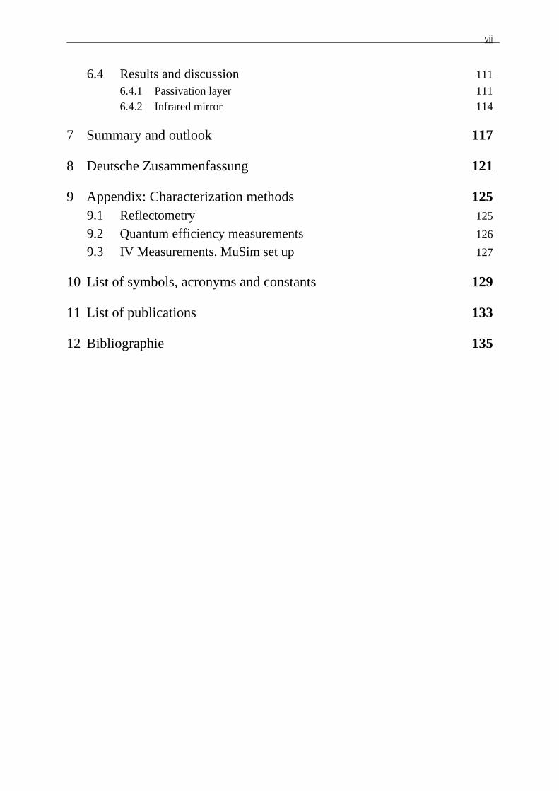
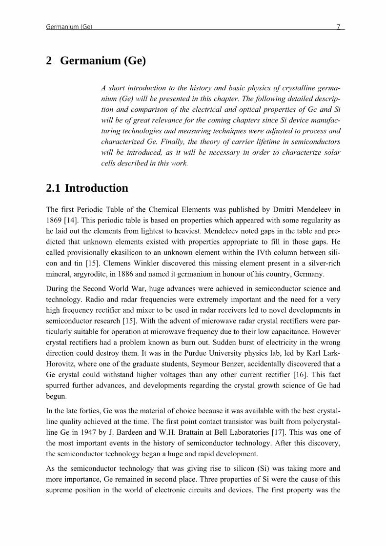
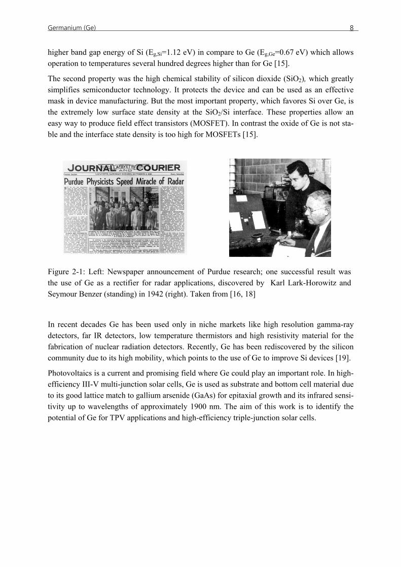
Figure 2-1: Left: Newspaper announcement of Purdue research; one successful result was the use of Ge as a rectifier for radar applications, discovered by Karl Lark-Horowitz and Seymour Benzer (standing) in 1942 (right). Taken from [16, 18]
Germanium (Ge)
9
The following sections of this chapter will present the basic properties of Ge. First, a brief report about crystal growth and crystalline structure will be given. Additionally, a description of the band structure of Si and Ge will provide a detailed explanation of the most important differences between both semiconductors.
2.2 Basics of Ge
2.2.1 Supply and crystal growth
Ge is found in different amounts as a component of certain minerals, such as: germanite (7CuS-FeS-GeS2), renierite (complex of Cu, Fe,Ge and As), argyrodite (4Ag2S-GeS2) and canfieldite (Ag8SnS6) with Ge content of 8.7%,7.8%, 6-7% and 1.8% respectively [21], [22]. These minerals have been mined in the past in Africa (Namibia and Congo), Germany and South America (Bolivia). However, the main sources for industrial production are found in zinc ores and coal and are located in Sakhalin Island (Russia), Mongolia and Lincang (west China). The world´s largest Ge producer is Teck Cominco Ltd in Canada. It processes ores and concentrates from the Red Dog zinc mine in Alaska and from other mines in the US, Canada and south America. Another region of interest is the “Big Hill” slag in the Democratic Republic of the Congo.
Contrary to Si, which is found in sand and quartz in the form of SiO2 (Si content 33.3%) processing is necessary in order to obtain Ge concentrate. As described above, the two main sources are zinc ores and coal. From the zinc ores the most common process to obtain Ge is the pyrometallurgical technique. In this process Ge is volatized in GeO or GeS, whereas from coal Ge volatizes as GeO and is concentrated in fly ashes [21],[22]. Both processes lead to Ge concentrations between 1 to 6 %. Ge is then sublimated in a smelter at a temperature of about 1200 °C. Ge with 5-30 % concentration is obtained from the fumes. After that, the fumes are chlorinated in concentrated hydrochloric acid. The following reaction takes place:
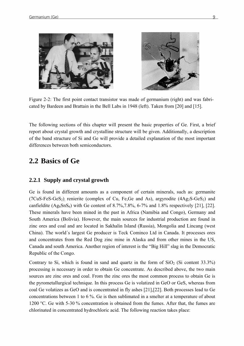
Figure 2-2: The first point contact transistor was made of germanium (right) and was fabri-cated by Bardeen and Brattain in the Bell Labs in 1948 (left). Taken from [20] and [15].
Germanium (Ge)
10
OHGeClHClGeO 242 24 +→+ Eq 2-1
By means of distillation process ultra pure GeCl4 is obtained.
Then the ultra pure GeCl4 is hydrolyzed with high-purity water to obtain GeO2:
HClGeOOHGeCl 42 224 +→+ Eq 2-2
After filtration and appropriate drying leads to various grades of GeO2. The pure Ge oxide is then reduced in an hydrogen atmosphere at 700 °C.
Single Ge crystals can be grown by various crystal growth techniques, but the most widely used method is the Czochralski crystal pulling technique [21]. In fact, Ge was the material on which the Czochralski crystal pulling technique was developed in 1950 by Teal and Little at Bell Labs. The Czochalski process to grow Ge is close to this for Si. It takes only some me-chanical adjustments and hot zone modifications to obtain Ge in the same machine. The growth process for Ge depends strongly on the specifications of the material, which is to be subsequently sliced, ground, and shaped for three main application fields: infrared thermal imaging, gamma-ray detectors, and opto-electronic substrates. For more information see [21]. The material used in this work was mono-crystalline germanium (c-Ge) grown by the Czochralski crystal pulling technique. It was obtained from Umicore in Belgium, which is the major European producer of high-purity Ge and Ge compounds. p-Ge samples were doped with gallium (Ga), whereas antimony (Sb) was used to dope n-Ge samples.
2.2.2 Band structure
In a single atom, the energy levels of an electron are discrete [10], [23]. However, bringing together many atoms, as is the case in a solid state, the discrete energy levels of the isolated atom spread into energy band as wave functions of electrons in neighboring atoms overlap; thus an electron is not necessarily located at a particular atom. This band structure can be cal-culated using different quantum mechanical approximations.
Si and Ge belong to the IVth column of the periodic table; they have similar electronic con-figurations and the same crystalline structure. However, there are important differences be-tween both semiconductors regarding their band structures.
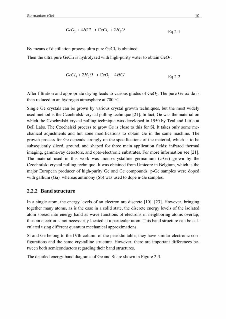
The detailed energy-band diagrams of Ge and Si are shown in Figure 2-3.
Germanium (Ge)
11
Figure 2-3: Band structure of Ge and Si. Taken from [24].
The energy is plotted as a function of the wave vector, k, along the main crystallographic di-rections <100> and <111>, since the band diagram depends on the direction within the crystal. An important feature of an energy-band diagram is whether the conduction band minimum and the valence band maximum occur at the same value for the wave number. If so, the en-ergy band gap is called direct. If not, as is the case for Si and Ge, the band gap is called indi-rect. Si has an indirect band gap of Eg=1.12 eV and a clearly higher direct transition of EΓ1=3.4 eV. Ge, however, has a lower indirect band gap of 0.67 eV and a very close direct transition of only EΓ1=0.8 eV (see Figure 2-3 and Table 2-3). This will determine the optical properties, as will be explained in the following.
2.3 Optical properties
As mentioned before, the maximum of the valence band and the minimum of the conduction band in Si and Ge do not have the same wave vector. This property defines an indirect semi-conductor. A transition from the maximum point of the valence band to the minimum point in the conduction band requires a change in wave vector, which results in a change of the mo-mentum of the electron. This change in momentum is brought about by a phonon which is needed in addition to the photon to make this absorption process possible. This is a three-particle process which is generally less likely than a two particle electron photon direct ab-sorption [25].
2.3.1 Electron-hole absorption
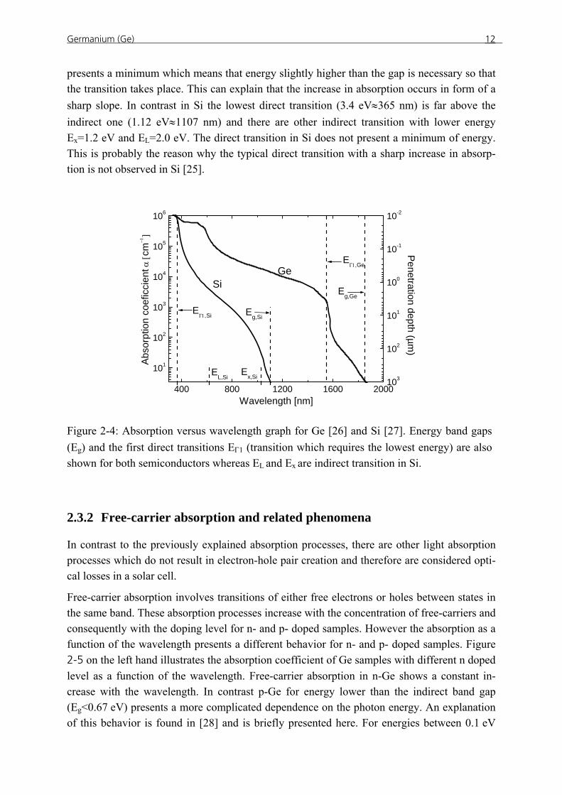
Although both semiconductors are indirect, their corresponding absorption behaviors are quite different (see Figure 2-4). Ge presents a small absorption for photons with energy in the range of the band gap (≈1850 nm). This is seen as a typical phenomenon for indirect band gaps. For values of wavelength below 1550 nm a steep increase follows. This is caused by the lowest direct transition, which occurs in Ge only 0.17 eV above the indirect band gap. This transition
Germanium (Ge)
12
presents a minimum which means that energy slightly higher than the gap is necessary so that the transition takes place. This can explain that the increase in absorption occurs in form of a sharp slope. In contrast in Si the lowest direct transition (3.4 eV≈365 nm) is far above the indirect one (1.12 eV≈1107 nm) and there are other indirect transition with lower energy Ex=1.2 eV and EL=2.0 eV. The direct transition in Si does not present a minimum of energy. This is probably the reason why the typical direct transition with a sharp increase in absorp-tion is not observed in Si [25].
400 800 1200 1600 2000
101
102
103
104
105
106
103
102
101
100
10-1
10-2
Ex,Si
Eg,SiE
Γ1,Si
EΓ1,Ge
Abs
orpt
ion
coef
icci
ent α
[cm
−1]
Wavelength [nm]
Eg,Ge
EL,Si
GeSi
Penetration depth (µm
)
Figure 2-4: Absorption versus wavelength graph for Ge [26] and Si [27]. Energy band gaps (Eg) and the first direct transitions EΓ1 (transition which requires the lowest energy) are also shown for both semiconductors whereas EL and Ex are indirect transition in Si.
2.3.2 Free-carrier absorption and related phenomena
In contrast to the previously explained absorption processes, there are other light absorption processes which do not result in electron-hole pair creation and therefore are considered opti-cal losses in a solar cell.
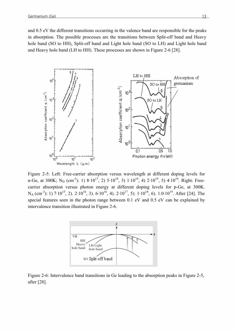
Free-carrier absorption involves transitions of either free electrons or holes between states in the same band. These absorption processes increase with the concentration of free-carriers and consequently with the doping level for n- and p- doped samples. However the absorption as a function of the wavelength presents a different behavior for n- and p- doped samples. Figure 2-5 on the left hand illustrates the absorption coefficient of Ge samples with different n doped level as a function of the wavelength. Free-carrier absorption in n-Ge shows a constant in-crease with the wavelength. In contrast p-Ge for energy lower than the indirect band gap (Eg<0.67 eV) presents a more complicated dependence on the photon energy. An explanation of this behavior is found in [28] and is briefly presented here. For energies between 0.1 eV
Germanium (Ge)
13
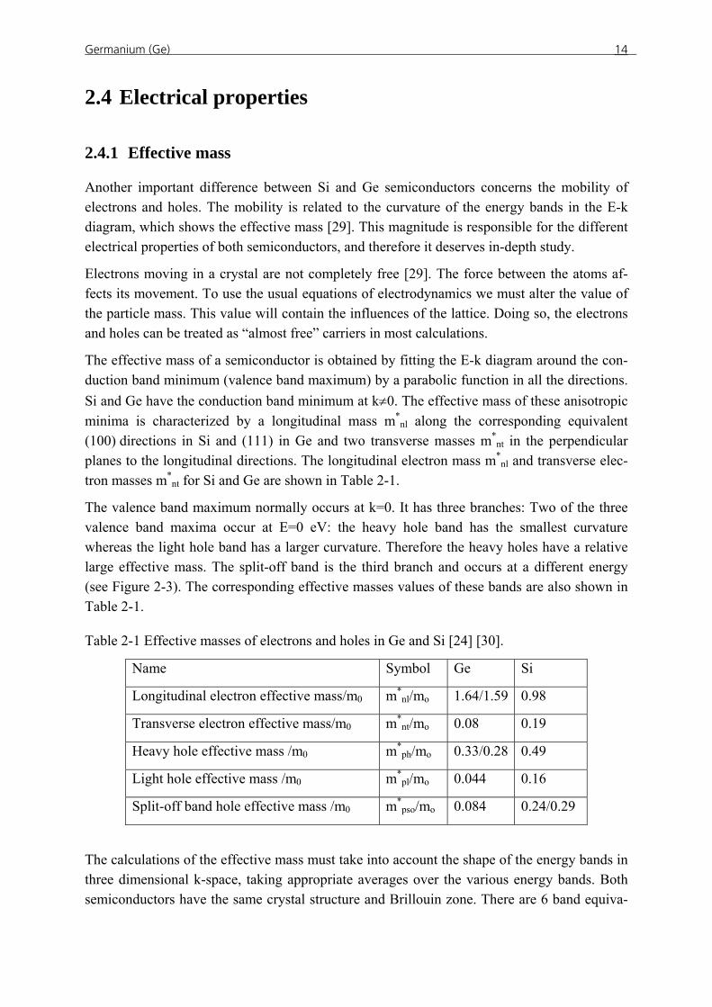
and 0.5 eV the different transitions occurring in the valence band are responsible for the peaks in absorption. The possible processes are the transitions between Split-off band and Heavy hole band (SO to HH), Split-off band and Light hole band (SO to LH) and Light hole band and Heavy hole band (LH to HH). These processes are shown in Figure 2-6 [28].
Figure 2-6: Intervalence band transitions in Ge leading to the absorption peaks in Figure 2-5, after [28].
Figure 2-5: Left: Free-carrier absorption versus wavelength at different doping levels for n-Ge, at 300K; ND (cm-3): 1) 8·1017, 2) 5·1018, 3) 1·1019, 4) 2·1019, 5) 4·1019. Right: Free-carrier absorption versus photon energy at different doping levels for p-Ge, at 300K. NA (cm-3): 1) 7·1015, 2). 2·1016, 3). 6·1016, 4). 2·1017, 5). 1·1018, 6). 1.0·1019. After [24]. The special features seen in the photon range between 0.1 eV and 0.5 eV can be explained by intervalence transition illustrated in Figure 2-6.
Germanium (Ge)
14
2.4 Electrical properties
2.4.1 Effective mass
Another important difference between Si and Ge semiconductors concerns the mobility of electrons and holes. The mobility is related to the curvature of the energy bands in the E-k diagram, which shows the effective mass [29]. This magnitude is responsible for the different electrical properties of both semiconductors, and therefore it deserves in-depth study.
Electrons moving in a crystal are not completely free [29]. The force between the atoms af-fects its movement. To use the usual equations of electrodynamics we must alter the value of the particle mass. This value will contain the influences of the lattice. Doing so, the electrons and holes can be treated as “almost free” carriers in most calculations.
The effective mass of a semiconductor is obtained by fitting the E-k diagram around the con-duction band minimum (valence band maximum) by a parabolic function in all the directions. Si and Ge have the conduction band minimum at k≠0. The effective mass of these anisotropic minima is characterized by a longitudinal mass m*
nl along the corresponding equivalent (100) directions in Si and (111) in Ge and two transverse masses m*
nt in the perpendicular planes to the longitudinal directions. The longitudinal electron mass m*
nl and transverse elec-tron masses m*
nt for Si and Ge are shown in Table 2-1.
The valence band maximum normally occurs at k=0. It has three branches: Two of the three valence band maxima occur at E=0 eV: the heavy hole band has the smallest curvature whereas the light hole band has a larger curvature. Therefore the heavy holes have a relative large effective mass. The split-off band is the third branch and occurs at a different energy (see Figure 2-3). The corresponding effective masses values of these bands are also shown in Table 2-1.
Table 2-1 Effective masses of electrons and holes in Ge and Si [24] [30].
Name Symbol Ge Si
Longitudinal electron effective mass/m0 m*nl/mo 1.64/1.59 0.98
Transverse electron effective mass/m0 m*nt/mo 0.08 0.19
Heavy hole effective mass /m0 m*ph/mo 0.33/0.28 0.49
Light hole effective mass /m0 m*pl/mo 0.044 0.16
Split-off band hole effective mass /m0 m*pso/mo 0.084 0.24/0.29
The calculations of the effective mass must take into account the shape of the energy bands in three dimensional k-space, taking appropriate averages over the various energy bands. Both semiconductors have the same crystal structure and Brillouin zone. There are 6 band equiva-
Germanium (Ge)
15
lent minima in Si (Six symmetry-related ellipsoids with long axis along <100>) and 4 in Ge (Eight symmetry-related half ellipsoids with long axis along <111>) [10].
Once the band curvature is determined, the components of the effective mass according to their crystalline orientation will be combined appropriately for different types of calcula-tions [30]. In order to determine the number of carriers in the bands the so called “density of states” effective masses ( *
,/ dospnm ) should be used. This parameter is obtained by taking the
geometric mean of the band curvatures, which are the effective masses, and the number of equivalent band extrema. On the other hand, in problems involving motion of carriers, one must consider the harmonic mean of the band curvature effective masses in order to get the value of conductivity effective masses ( *
,/ condpnm ) (see Table 2-2). For details regarding the calculations of these values see
[30].
Table 2-2 Density of states and conductivity effective masses in Si and Ge [29, 30]. The two different values reflect two different literature sources used.
Name Symbol Ge Si
Density of states electron effective mass *,dosnm /mo 0.55/0.56 1.1
Density of states hole effective mass *,dospm /mo 0.37/0.29 0.57/0.81
Conductivity electron effective mass *,condnm /mo 0.12 0.26
Conductivity hole effective mass *,condpm /mo 0.21 0.38/0.36
2.4.2 Carrier densities
The density of electrons in a semiconductor depends on the density of available states and their probability of occupation [11].
At absolute zero T(K)=0 electrons in a crystal occupy the lowest possible energy states. The highest occupied level is known as the Fermi level EF. With increasing temperature, some electrons gain energy higher than EF. The probability of occupation of an allowed state of any given energy E can be calculated from statistical considerations that take into account the re-striction of the Pauli exclusion principle which result in the Fermi-Dirac distribution function:
⎟⎟⎠
⎞⎜⎜⎝
⎛ −+
=
TkEE
Ef
B
Fexp1
1)( Eq 2-3
Germanium (Ge)
16
Where EF is the Fermi energy, kB is the Bolzmann constant and T the absolute temperature.
The densities of allowed states D(E) in the conduction band and the valence band respectively are given by:
( ) ( ) 2/12/3*,)( CdosnC EEmED −∝ Eq 2-4
( ) ( ) 2/12/3*,)( EEmED VdospV −∝ Eq 2-5
Where ( )*,dosnm and ( )*
,dospm denote the densities of states effective masses (Table 2-2).
Knowing the density of allowed states D(E) and the probability of occupation of these states, the density of electrons n and holes p respectively as follows [11]:
∫∞
=CE
C dEEfEDn )()( Eq 2-6
∫ −=VE
v dEEfEDp0
))(1)(( Eq 2-7
Since EC-EF >>kT, f(E) can be approximated by the Boltzmann distribution which simplifies greatly these equations, leading in thermal equilibrium to:
⎟⎟⎠
⎞⎜⎜⎝
⎛ −−=
TkEENn
B
FCC exp0 Eq 2-8
⎟⎟⎠
⎞⎜⎜⎝
⎛ −−=
TkEENp
B
VFV exp0 Eq 2-9
Where NC/V is the effective density of states in the conduction/valence band and can be ex-pressed as:
2/3
2
*,/
/
22 ⎟
⎟⎠
⎞⎜⎜⎝
⎛=
hTkm
N BdospnVC
π
Eq 2-10
The intrinsic carrier concentration ni is defined via the product of n0 and p0:
Germanium (Ge)
17
⎟⎟⎠
⎞⎜⎜⎝
⎛−==
TkE
NNpnnB
gVCi exp00
2 Eq 2-11
For the ideal case of a pure and perfect semiconductor, where n=p these equations are valid because each electron in the conduction band leaves a vacancy or hole in the valence band. In this case, the Fermi level is close to the mid-gap energy.
In this point it is interesting to remark that the intrinsic carrier concentration ni in Ge is higher than in Si (see Table 2-3), even though there exists a smaller density of states effective mass mn/p*,dos in Ge (see Table 2-2). Responsible for this is the smaller Eg in Ge, which is the domi-nant term in Eq 2-11. This will also result in a smaller voltage of Ge solar cells compared to Si.
Table 2-3 Basic parameters in Ge and Si [11][24].
Eg
(eV) EΓ1
(eV)
ni
(cm-3)
Mobility electrons
(cm2V-1s-1)
Mobility holes
(cm2V-1s-1)
Ge 0.67 0.8 2·10 13 3900 1900
Si 1.12 3.4 1·10 10 1400 450
2.4.3 Conductivity and mobility
Drift
In the presence of an electric field an electric current flows though a semiconductor. The ease with which charge carriers drift in the material depends on the intrinsic properties and the defects in the material.
The drift current density Jdrift,x (in x direction) in a semiconductor is proportional to the elec-tric field E.
xxdrift EJ σ=, Eq 2-12
The factor of proportionality is called the conductivity σ (Ω·cm)-1 and for electrons can be written in terms of a mobility µn which describes the ability of electrons to move through the crystal [29] as
Germanium (Ge)
18
nn qnµ=σ where *,condn
n mqτμ = Eq 2-13
Where q denotes the electronic charge, *,condnm is the conductivity effective mass for electrons
and τ represents the mean time between scattering events, which is a function of the tempera-ture and is related to the defects in the crystal.
An analogous equation for holes is:
pp qnµ=σ where *,condp
p mqτμ = Eq 2-14
where *,condpm is the conductivity effective mass for holes.
The drift current density for electrons can be written as a function of the mobility:
nEqµJ ndriftn =, Eq 2-15
An analogous equation for holes in the valence band is:
pEqµJ pdriftp =, Eq 2-16
The sum of these two components gives the total current density Jdrift=Jn,drift+Jp,drift. Hence, the conductivity σ of the semiconductor can be expressed as:
pqnq pn μμρ
σ +==1
Eq 2-17
where ρ is the resistivity.
According to Eq 2-13, the parameters which determine the mobility are the conductivity ef-fective mass ( *
,/ condpnm ) and the mean free time τ. As the effective mass in Ge is smaller than
in Si, a higher mobility is obtained. Figure 2-7 shows the variation of mobility with doping concentration at room temperature for both semiconductors.
Germanium (Ge)
19
1014 1015 1016 1017
1000
2000
3000
4000
Sihole
hole
electron M
inor
ity c
arrie
r mob
ility
[cm
2 /Vs]
Doping concentration [cm -3]
electron
Ge
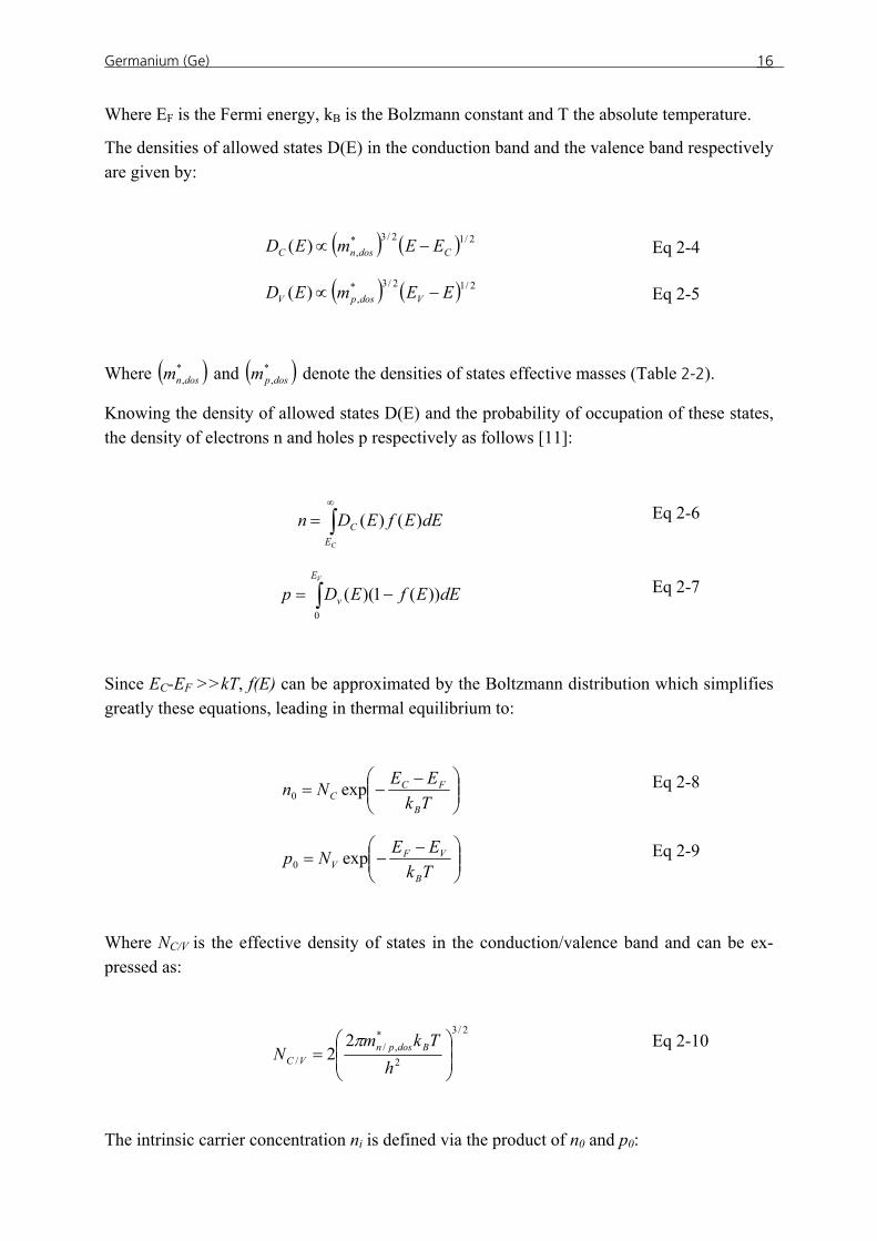
Figure 2-7: Minority carrier mobility as a function of doping concentration for Si and Ge, data taken from [31].
Diffusion Carriers in a semiconductor can also flow by diffusion. The flux of particles and therefore the diffusion current density is proportional to the concentration gradient. Since the diffusion cur-rent flows from high to low density regions a minus sign needs to be included in Eq 2-19.
dxdnqDJ ndiffn =, Eq 2-18
dxdpqDJ pdiffp −=, Eq 2-19
Dn and Dp are the diffusion constants for electrons and holes respectively. Drift and diffusion processes are fundamentally related to mobility and diffusion constants and are connected by the Einstein relations:
nn qkTD μ= Eq 2-20
pp qkTD μ= Eq 2-21
The purpose of these calculations was to show that the difference between Ge and Si resides from the band structure. The small direct band gap of Ge leads to high absorption below 1550 nm. Otherwise the curvature of the conduction and valence band is responsible for the higher mobility of the carriers in Ge. On the other hand, the smaller indirect energy band gap
Germanium (Ge)
20
leads to a very high intrinsic carrier concentration (Eq 2-11 and Table 2-3) which will result in a very small voltage in Ge cells.
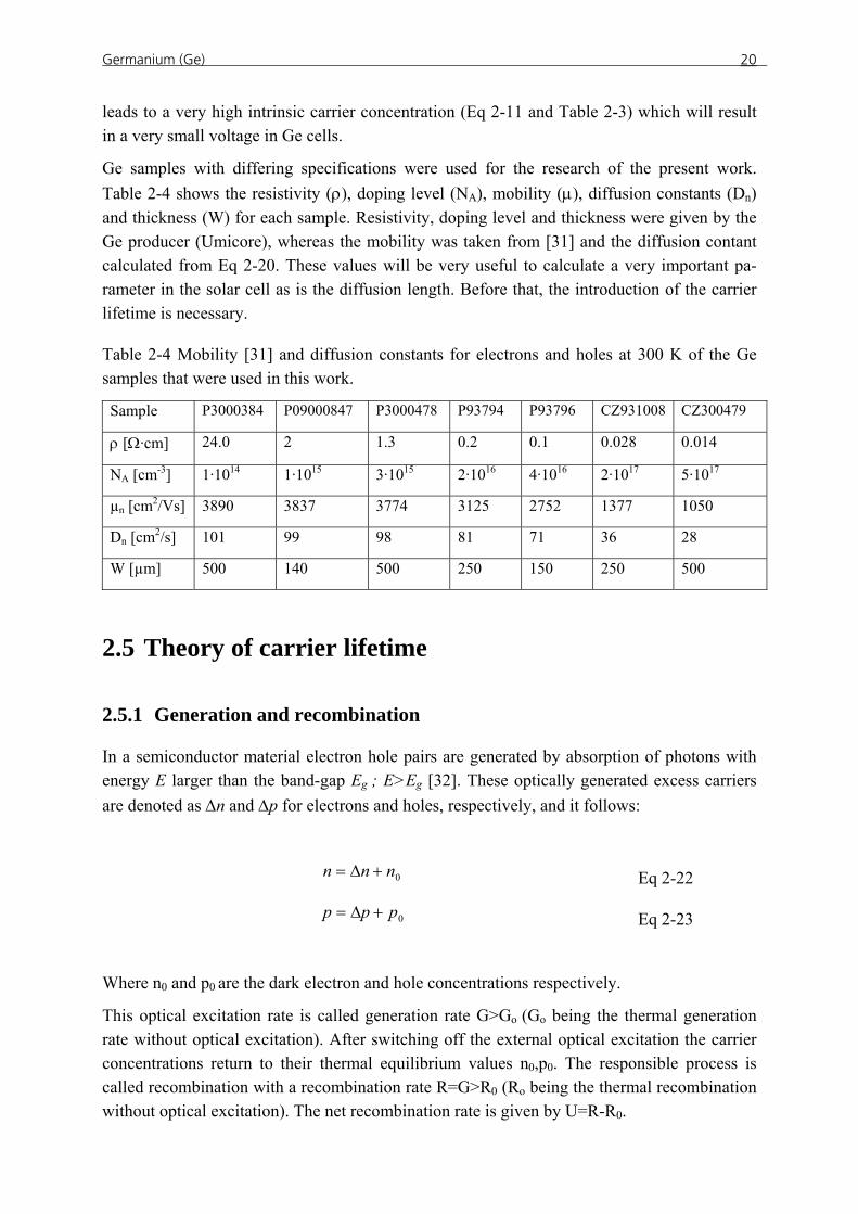
Ge samples with differing specifications were used for the research of the present work. Table 2-4 shows the resistivity (ρ), doping level (NA), mobility (μ), diffusion constants (Dn) and thickness (W) for each sample. Resistivity, doping level and thickness were given by the Ge producer (Umicore), whereas the mobility was taken from [31] and the diffusion contant calculated from Eq 2-20. These values will be very useful to calculate a very important pa-rameter in the solar cell as is the diffusion length. Before that, the introduction of the carrier lifetime is necessary.
Table 2-4 Mobility [31] and diffusion constants for electrons and holes at 300 K of the Ge samples that were used in this work.
Sample P3000384 P09000847 P3000478 P93794 P93796 CZ931008 CZ300479
ρ [Ω·cm] 24.0 2 1.3 0.2 0.1 0.028 0.014
NA [cm-3] 1·1014 1·1015 3·1015 2·1016 4·1016 2·1017 5·1017
µn [cm2/Vs] 3890 3837 3774 3125 2752 1377 1050
Dn [cm2/s] 101 99 98 81 71 36 28
W [µm] 500 140 500 250 150 250 500
2.5 Theory of carrier lifetime
2.5.1 Generation and recombination
In a semiconductor material electron hole pairs are generated by absorption of photons with energy E larger than the band-gap Eg ; E>Eg [32]. These optically generated excess carriers are denoted as Δn and Δp for electrons and holes, respectively, and it follows:
0nnn +Δ= Eq 2-22
0ppp +Δ= Eq 2-23
Where n0 and p0 are the dark electron and hole concentrations respectively.
This optical excitation rate is called generation rate G>Go (Go being the thermal generation rate without optical excitation). After switching off the external optical excitation the carrier concentrations return to their thermal equilibrium values n0,p0. The responsible process is called recombination with a recombination rate R=G>R0 (Ro being the thermal recombination without optical excitation). The net recombination rate is given by U=R-R0.
Germanium (Ge)
21
Considering the charge neutrality and the absence of minority carrier trapping centers, which means that Δn=Δp, the time dependent decay of excess carriers is given by:
( ) ( )00 ,),( pntnUt
tnΔ−=
∂Δ∂
Eq 2-24
The recombination lifetime, often also referred to as minority carrier lifetime, corresponds to the time constant of the exponential decay and is defined via the following equation:
( ) ( )0000 ,,
,,pnnU
npnnΔ
Δ=Δτ Eq 2-25
The carrier lifetime generally depends strongly on the injection density as well as on the dop-ing concentration of the semiconductor via n0 and p0.
The three fundamental recombination processes in a semiconductor are the radiative recombi-nation, Auger recombination and Shockley-Read-Hall recombination. These recombination mechanisms occur independently from each other in the semiconductor and therefore the total recombination rate UTotal can be expressed as the sum of the individual recombination rates.
∑=i
iTotal UU Eq 2-26
According to Eq 2-25 the inverse total carrier lifetime then equals the sum of the inverse indi-vidual carrier lifetimes:
∑=i iTotal ττ
11
Eq 2-27
2.5.2 Carrier recombination mechanism
The three fundamental recombination processes can be classified in intrinsic and extrinsic recombination mechanisms.
The intrinsic recombination mechanisms depend on the intrinsic material properties (band structure). They belong to the semiconductor and therefore are unavoidable. The two intrinsic processes are the radiative and Auger recombination.
Germanium (Ge)
22
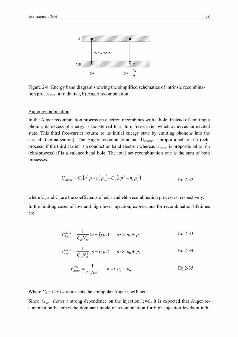
Radiative recombination
In the radiative process an electron in the conduction band falls into a non occupied state in the valence band (hole). This mechanism leads to the direct annihilation of an electron-hole pair, which results in the emission of a photon with energy approximately equal to the band gap (Figure 2-8 a). Since the process requires free electrons and free holes the radiative re-combination rate depends strongly on the concentration of free electrons n and free holes p.
( )2iRad nnpBU −= Eq 2-28
Where B is a material constant and contains the quantum-mechanical probability of a radia-tive transition. This value depends basically on the band structure of the semiconductor.
In direct semiconductors like GaAs, radiative recombination is a dominant process since the transitions occur vertically in the E-k space and the emission of a photon is only necessary to conserve energy and momentum. In an indirect semiconductor like Si however an additional particle (phonon) is necessary to conserve the momentum. In this case radiation is not the dominant process, this is reflected in the value of B (B=1·10-14 cm3/s ) for Si, which is four orders of magnitude smaller than in GaAs (B=3·10-10 cm3/s) [32].
In the case of Ge the value of B (B=6.4 10-14cm3/s) [24] is a factor 6 higher than in Si. This can be explained from the band structure in Ge. Its lowest direct transition energy is only 0.14 eV larger than its indirect band gap, which leads to a higher probability of radiative tran-sitions.
The corresponding recombination rate URad and carrier lifetime τRad considering charge neu-trality Δn=Δp is given by
nBpnBnBnpnBU RadRad Δ++
=⇒Δ+Δ+=)(
1)(00
200 τ
Eq 2-29
In the limiting cases of low-level injection (LLI) and high-level injection (HLI) the common relationships are:
Dot
LLIRad BN
1=τ (Δn<<n0+p0) Eq 2-30
nBHLIRad Δ
=1τ (Δn>>n0+p0) Eq 2-31
Germanium (Ge)
23
Auger recombination
In the Auger recombination process an electron recombines with a hole. Instead of emitting a photon, its excess of energy is transferred to a third free-carrier which achieves an excited state. This third free-carrier returns to its initial energy state by emitting phonons into the crystal (thermalization). The Auger recombination rate UAuger is proportional to n2p (eeh-process) if the third carrier is a conduction band electron whereas UAuger is proportional to p2n (ehh-process) if is a valence band hole. The total net recombination rate is the sum of both processes:
( ) ( )200
20
20
2 pnnpCpnpnCU pnAuger −+−= Eq 2-32
where Cn and Cp are the coefficients of eeh- and ehh-recombination processes, respectively.
In the limiting cases of low and high level injection, expressions for recombination lifetimes are:
)(12
, TypenNC Dn
nLLIAuger −=τ 00 pnn +<< Eq 2-33
)(12
, TypepNC Ap
pLLIAuger −=τ 00 pnn +<< Eq 2-34
21
nCa
HLIAuger Δ
=τ 00 pnn +>> Eq 2-35
Where Ca =Cn+Cp represents the ambipolar Auger coefficient.
Since τAuger shows a strong dependence on the injection level, it is expected that Auger re-combination becomes the dominant mode of recombination for high injection levels in indi-
Figure 2-8: Energy band diagram showing the simplified schematics of intrinsic recombina-tion processes: a) radiative, b) Auger recombination.
Germanium (Ge)
24
rect semiconductors. This is clearly the case for Si. In Ge, however, due to the higher value of the radiative recombination constant B (see Eq 2-28), a combination of both radiative and Auger recombination mechanisms occur. This will be discussed in Chapter 4.
Having seen the impact of intrinsic recombination mechanisms in the previous sections, the extrinsic recombination via defects in the bulk and at interfaces is discussed in the following. As bulk recombination via defects (Shockley-Read-Hall) [11] is mathematically equivalent to surface recombination, first the impact of the most important parameters in Shockley-Read-Hall recombination will be discussed, and then it will be generalized for the surface recombination adjusting to the necessary parameters according to the difference be-tween both mechanisms.
Shockley-Read-Hall recombination
Dislocations and impurities lead to allowed intermediate energy levels in the band gap [33]. These “defects” or “traps” are responsible for a two step recombination process (see Figure
2-9(a)). This recombination process depends on the crystal growth technique and the quality of the starting material and since it is not related to the semiconductor intrinsic properties is called an extrinsic recombination process.
The analysis of the dynamics of this process can be found in [32] and [33]. The special case of the net recombination rate USRH (unit cm-3s-1) for a single defect placed at an energy level Et is
)()( 1010
2
ppnnnnpU
np
iSRH +++
−=
ττ Eq 2-36
τpo and τno are the capture time constants of holes and electrons, which are related to the defect concentration Nt, the thermal velocity νth of charge carriers and the capture cross-sections σn and σp of the specific defect center in question as follows.
( ) 10
−= thptp N νστ
( ) 10
−= thntn N νστ
Eq 2-37
n1 and p1 are parameters related to the trapping level Et [32].
Germanium (Ge)
25
⎟⎠⎞
⎜⎝⎛ −
=kT
EENn Ct
c exp1 , ⎟⎠⎞
⎜⎝⎛ −
=kT
EENp tV
V exp1 Eq 2-38
211 inpn = Eq 2-39
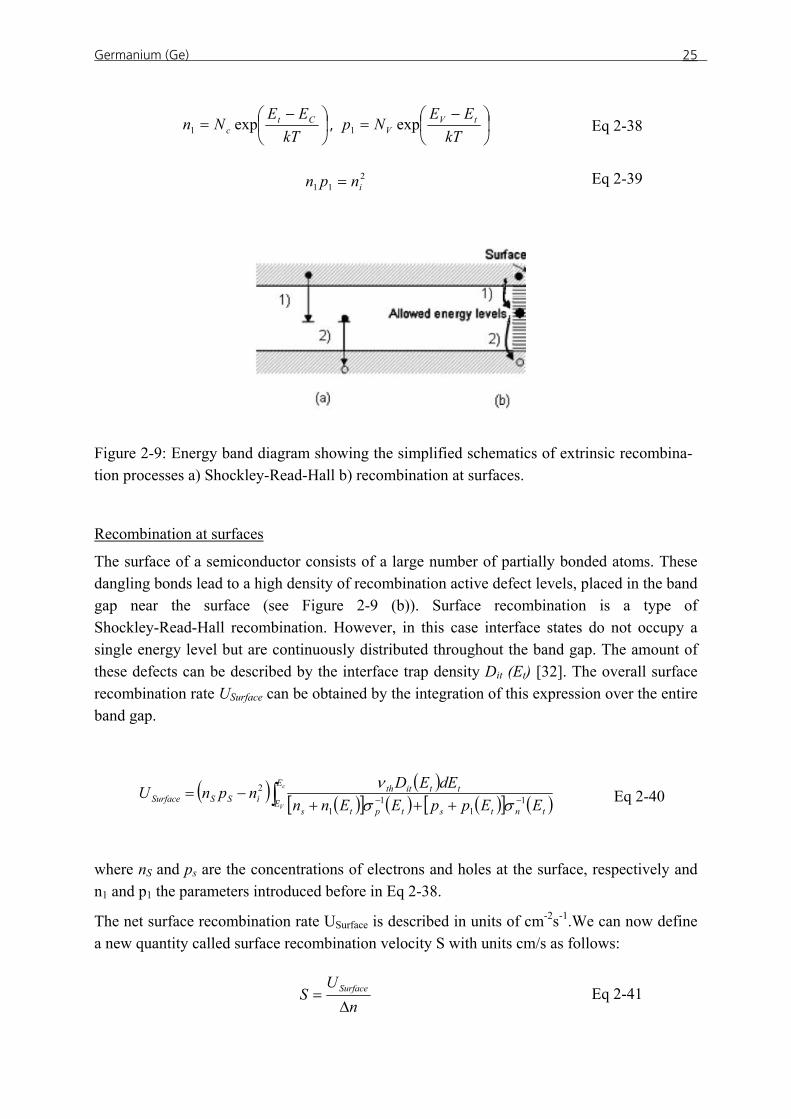
Figure 2-9: Energy band diagram showing the simplified schematics of extrinsic recombina-tion processes a) Shockley-Read-Hall b) recombination at surfaces.
Recombination at surfaces
The surface of a semiconductor consists of a large number of partially bonded atoms. These dangling bonds lead to a high density of recombination active defect levels, placed in the band gap near the surface (see Figure 2-9 (b)). Surface recombination is a type of Shockley-Read-Hall recombination. However, in this case interface states do not occupy a single energy level but are continuously distributed throughout the band gap. The amount of these defects can be described by the interface trap density Dit (Et) [32]. The overall surface recombination rate USurface can be obtained by the integration of this expression over the entire band gap.
( ) ( )( )[ ] ( ) ( )[ ] ( )∫ −− +++
−= c
V
E
Etntstpts
ttitthiSSSurface EEppEEnn
dEEDnpnU 11
11
2
σσν
Eq 2-40
where nS and ps are the concentrations of electrons and holes at the surface, respectively and n1 and p1 the parameters introduced before in Eq 2-38.
The net surface recombination rate USurface is described in units of cm-2s-1.We can now define a new quantity called surface recombination velocity S with units cm/s as follows:
nU
S Surface
Δ= Eq 2-41
Germanium (Ge)
26
In order to calculate the surface recombination velocity parameters of electrons Sn0 and holes Sp0 experimental data for the quantities Dit (Et), σn(Et), σp(Et) are needed, as well as ns and ps.
A detailed discussion can be found in [32] A discussion of the injection dependence of the surface recombination velocity S is found in [33].
Eq 2-42 shows the different parameters of Sp0 and Sn0.
),,,,(00 ssthpitpp pnDSS νσ=
),,,,(00 ssthnitnn pnDSS νσ=
Eq 2-42
As the surface recombination velocity is related to the fundamental properties of the surface defects, it is a direct measure for the recombination activity of the surface.
To find a way to reduce the surface recombination rate USurface in Ge will be one of the most important challenges in this work. The technology which allows a reduction of the surface recombination velocity is called passivation and will be further discussed in chapter 4. Mate-rial lifetime measurements will be discussed in chapter 3 in detail. The way to obtain the sur-face recombination velocity by means of lifetime measurements will be explained in the fol-lowing.
2.5.3 Effective lifetime and separation of bulk lifetime
When measuring the excess carrier lifetime of a semiconductor sample, an effective lifetime is actually measured, which includes all recombination channels discussed above, and can be calculated using Eq 2-27:
SurfaceBulkSurfaceSRHAugerRadeff τττττττ1111111
+=+⎟⎟⎠
⎞⎜⎜⎝
⎛++= Eq 2-43
An important point in this work is to know the impact of surface recombination on the effec-tive carrier lifetime; in other words, the quality of the passivation layer. This requires a sepa-ration of bulk and surface recombination velocity. Considering a test structure with identically passivated wafer surfaces (S1=S2=S), an approximation [34] for the surface recombination velocity τSurface for sufficiently low S values is given by:
Germanium (Ge)
27
In this formula W is the sample thickness and Dn/p the diffusion constant of the minority carri-ers as defined in Eq 2-20 and Eq 2-21.
From these equations it is clear that the surface recombination velocity can be extracted from lifetime measurements of τeff if the bulk lifetime is known. A method to determine the bulk lifetime for a certain doping level is to measure the effective lifetime on different wafers with exactly the same specifications except the thickness. Measuring the effective lifetime for vari-ous thicknesses, preferably three or more, leads to multiple equations with two unknown val-ues (Seff and τBulk), which can be subsequently solved. The quality of the surface passivation will be characterized using this method, as will be explained in Chapter 3.
Once we have discussed concepts like the diffusion constant and effective lifetime, we can introduce an important quantity in solar cells: the minority carrier diffusion length.
effpnpn DL τ⋅= // Eq 2-45
Where Dn/p is the diffusion constant and τeff is the measured lifetime in the sample.
The diffusion length is the average distance a minority carrier can move from the point of generation until it recombines. A high effective minority carrier diffusion length is crucial to achieve maximized conversion efficiency in a solar cell, as will be discussed in chapter 4. In the next section, the applied measurement technique to determine the minority carrier density will be discussed.
WS
Surface
21=
τ for
WD
S pn /2<< Eq 2-44

Germanium (Ge)
28
Lifetime measurements
29
3 Lifetime measurements
This chapter will discuss the microwave detected photoconductance decay
technique (MW-PCD), which was the characterization method used in the pre-
sent work for measuring the effective carrier lifetime in Ge samples. First of
all, a general description of the measurement set up will be given. Since this
method was originally developed and used for Si materials, a discussion of the
measurement validity for Ge samples will be presented by means of theoreti-
cal calculations.
3.1 Introduction
The different techniques to measure the lifetime in a semiconductor can be classified by the time dependence of illumination. The first regime involves a sharp pulse of illumination that is rapidly turned off and, subsequently, the excess carrier density without illumination is de-termined. This corresponds to the transient technique developed by [35, 36]. The second method is the quasi steady-state illumination, first introduced by Sinton and Cuevas [37], where the illumination intensity is slowly reduced to zero over several milliseconds.
All these methods were developed to measure the lifetime in Si samples. In this work, the traditional transient technique was used for measuring the effective carrier lifetime in Ge samples, since in comparison to the Quasi-steady-state photoconductance technique (QSSPC) this is the technique that requires fewer changes in the measurement set up. Due to the differ-ent specifications of Ge samples in comparison to Si, the measurement conditions were dif-ferent. Theoretical simulations of the measurements were carried out and the validity of the measurement at low injection conditions was demonstrated. This technique was used for the characterization of passivation layers developed in this work. Furthermore, the bulk lifetime was determined in Ge for different doping concentration. This will be shown in chapter 4. Additionally, the lifetime measurement set up and consideration at high injection condition will be presented in the last section.
3.2 Microwave-detected photoconductance decay technique
3.2.1 Measurement principle
The microwave-detected photoconductance (MW-PCD) technique is a purely transient tech-nique, which measures the exponential decay of excess carriers immediately after a short laser pulse [38], [33]. In this system, a short laser pulse (904 nm) on top of a steady state bias light generates excess carriers within the investigated wafer. This leads to an increase of the wafer
Lifetime measurements
30
conductance. After termination of each pulse, the excess carriers diffuse and recombine within the bulk and at both surfaces of the wafer and the photo-conductance decreases expo-nentially to its initial value. From the bottom, microwaves of a frequency of 2.8 GHz gener-ated in a phase-locked microwave oscillator are directed through a waveguide and the re-flected microwaves are redirected towards the detector. Depending on the sample conduc-tance, the signal is reflected with varying intensity. The output of the detector diode, which is proportional to the reflected microwave power, is then amplified. The time dependence of this quantity is recorded by a digital storage oscilloscope and then analyzed by means of a com-puter.
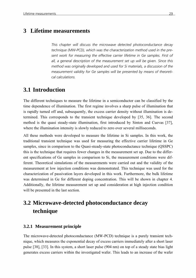
The MW-PCD measurement system [39], [40], [41] was realized at Fraunhofer ISE and is shown in Figure 3-1.
Figure 3-1: (Left) Schematic diagram of the MW-PCD setup which consist of the microwave set up, the sample holder, the bias light illumination and the pulsed laser. (Right) MW-PCD setup used for the measurements in this work.
The relationship between the electrical conductance and the free-carrier density in a homoge-neously doped piece of semiconductor is linear [42]:
)( pnq pn μμσ += Eq 3-1
where q denotes the elementary charge, µn/p the mobility of electrons and holes and n/p the carrier densities of the electrons and holes.
For some reason explained later it is necessary to assure that the change in the photoconduc-tivity due to the laser excitation is proportional to the laser induced carrier density. The change in conductivity due to the laser excitation can be expressed by:
Lifetime measurements
31
( ) ( )biasbiasbiaslaserbiaslaserbiaslaser npnnpp ,, σσσ −Δ+Δ+=Δ Eq 3-2
Assuming a low change of carrier densities Δnlaser<nbias and Δnlaser=Δplaser leads to the follow-ing approximation which means that the relationship between the change in conductivity and the excess carrier density is still linear.
( ) laserpnlaser nq Δ⋅+=Δ μμσ ( biasbiaslaserlaser pnpn ,<Δ=Δ ) Eq 3-3
Since the microwave reflectance is a highly non linear function of the conductance [39], the MW-PCD technique is restricted to low excitation densities and small changes in the excita-tion intensity. Only small intervals (Δσlaser/ σbias<10%) can be treated as quasi-linear. That means that the additional conductivity acquired due to the laser excitation (Δσlaser) has to be small compared to the conductivity due to the additional bias light (σbias). Therefore, this should be taken into account during the measurement: the laser power (filters) must be ad-justed in order to achieve a small signal which then assures a correct measurement (see Figure
3-2). In the following Δnlaser will be written as Δn to simplify the equations.
3.2.2 Transient decay study of minority carrier lifetime in Ge
In the present work the microwave – detected photoconductance method has been used to measure the minority carrier lifetime in Ge. In the following a calculation of the excess carrier density as a function of the time and position will be carried out. In the measurement system, which was developed for Si samples, an GaInAs diode laser (904 nm) with a pulse length of 100 ns was used. Maximum laser pulse energy at the sample surface is 12 mJ, corresponding to 5·1013 photons per pulse. A penetration depth of 50 µm is expected for Si, whereas only 400 nm is achieved in Ge (see Figure 2-4 in Chapter 2). Due to the high absorption within Ge a very high influence of the surface condition is expected. Theoretical simulations of the ex-cess carrier densities as a function of the position (Wafer depth) and time, Δn(x,t) were carried out in order to assure the validity of the measurement and understand the influence of the specifications of Ge samples such as the surface passivation quality, the diffusion constant of the minority carriers and the absorption within the wafer.
The carrier lifetime analysis is based on previous work by Ogita [43] and Glunz [39]. The set up is illustrated in Figure 3-2 (left). The following assumptions are used in the analysis: 1) the excess minority carrier density is everywhere small compared to the majority carrier density, 2) that the electron-hole pairs recombine within the bulk lifetime τBulk, and 3) that both the front and back surfaces of the sample have the same surface recombination velocity S. The sample is a planar wafer of uniformly NA doped p-type Ge. Its thickness W is small compared to the other directions y and z; consequently, the excess carrier density distribution produced by the laser pulse essentially varies only along the x direction. In this case, it is possible to use
Lifetime measurements
32
the one dimensional form of the time dependent continuity equation to determine the excess minority carrier density as a function of distance and time Δn(x,t). This is justified as long as the diffusion length for lateral diffusion is much smaller than the illumination laser spot. Here only a brief discussion of the dynamics of minority carrier concentration will be given. For a detailed analysis of this problem, see [44] and [45].
The excess minority carrier concentration Δn(x,t) is described by the time dependent continu-ity equation:
)exp()(),(),(),( 2
2
/ xttxntxnx
Dtxnt Bulk
pn αατ
−Φ+Δ
−Δ∂∂
=Δ∂∂
Eq 3-4
The terms on the right hand side of Eq 3-4 correspond to diffusion*, recombination and gen-eration, respectively. φ(t) is the time dependent internal photon flux density multiplied by the quantum efficiency of the minority carrier density generation [39].
050
60
70
80
90
100
110
120
Aditional Bias light
Short laser pulseΔnbias+Δnlas
Δn
(a.u
.)
Time
Δnbias
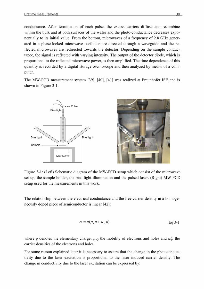
Figure 3-2: Left. Schematic of a MW-PCD measurement set-up. Additional to the steady-state bias light, a short laser pulse generates electron hole pairs within the semiconductor sample. After the short laser pulse, these electron hole pairs diffuse and recombine. The figure on the right shows the time dependence of the excess carrier density generated by the short laser pulse and the additional bias light.
*The general expression [11],[33] uses the ambipolar diffusion coefficient Da which applies to all injection levels. Here is assumed that n<<p in p-type semiconductor and p<<n in n-type semicon-ductor. In this case Da can be approximated to Dn and Dp in p-type and n-type material respec-tively.
Lifetime measurements
33
The local density of the excess carriers in Ge Δn(x,t) is obtained by solving the continuity equation Eq 3-4 with proper initial and boundary conditions. By means of Fourier transforma-tions and several mathematic manipulations [39, 45] the following solution of the time de-pendent equation for the excited minority carrier concentration Δn(x,t) after a δ-pulse is ob-tained.
m
t
m
M
mexCtxn τ
δπ
−
=∑Φ=Δ )(
21),(
1 Eq 3-5
with Cm given by
⋅⎥⎥⎦
⎤
⎢⎢⎣
⎡
+= 22
22
m
mmC
γααγπ
( )( ) ( )( ) ( ) ( )
( ) ( ) ⎥⎥⎥⎥⎥
⎦
⎤
⎢⎢⎢⎢⎢
⎣
⎡
⎟⎟⎠
⎞⎜⎜⎝
⎛−+−⎟
⎟⎠
⎞⎜⎜⎝
⎛+
⎥⎥⎦
⎤
⎢⎢⎣
⎡+⎟
⎟⎠
⎞⎜⎜⎝
⎛−−
⎥⎥⎦
⎤
⎢⎢⎣
⎡−+−⎟
⎟⎠
⎞⎜⎜⎝
⎛+ −
WWD
WSD
SWDSW
xD
SxeD
SxWD
SxWD
S
mmpnpn
mmpn
mpn
mmW
pnm
pnmm
pn
γγγγ
γγγαγγγα α
cos2sin22
sincossincos
22
/
2
//
////
Eq 3-6
msBulkm ,
111τττ
+= with 2/
,1
mpnms D γ
τ = Eq 3-7
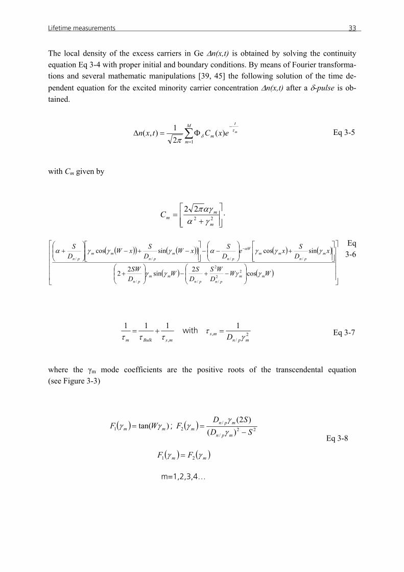
where the γm mode coefficients are the positive roots of the transcendental equation (see Figure 3-3)
( ) )tan(1 mm WF γγ = ; ( ) 22/
/2 )(
)2(SD
SDF
mpn
mpnm −
=γγ
γ
( ) ( )mm FF γγ 21 =
m=1,2,3,4…
Eq 3-8
Lifetime measurements
34
Figure 3-3: Calculation of the modes γm (with m=1,2,3…) as a solution of F1(γm)=F2(γm).
It is interesting to remark that these coefficients γm do not depend on the bulk lifetime τBulk but rather on the surface recombination velocity S, the thickness W and the diffusion constant Dn/p.
Mathematically, the function Δn(x,t) in Eq 3-5 is the sum of the exponential decays of indi-vidual modes, each represented by an individual time constant τm and weighted by a coeffi-cient Cm (Similar to a vibrational spectrum, which is composed of different modes). This means that one can not, in general, expect to find a single exponential decay with one time constant. However, in many cases, the decay is found to be multiexponential at the beginning of the decay. After few µs the first mode γ1 dominates and the decay can be approximated by a single exponential decay with a time constant τ1. This value is called effective lifetime and is smaller than the bulk lifetime τBulk (Eq 3-7). The decay time of this single exponential decay depends strongly on the surface recombination velocity S, on the thickness W and on the dif-fusion constant Dn, as will be presented as follows.
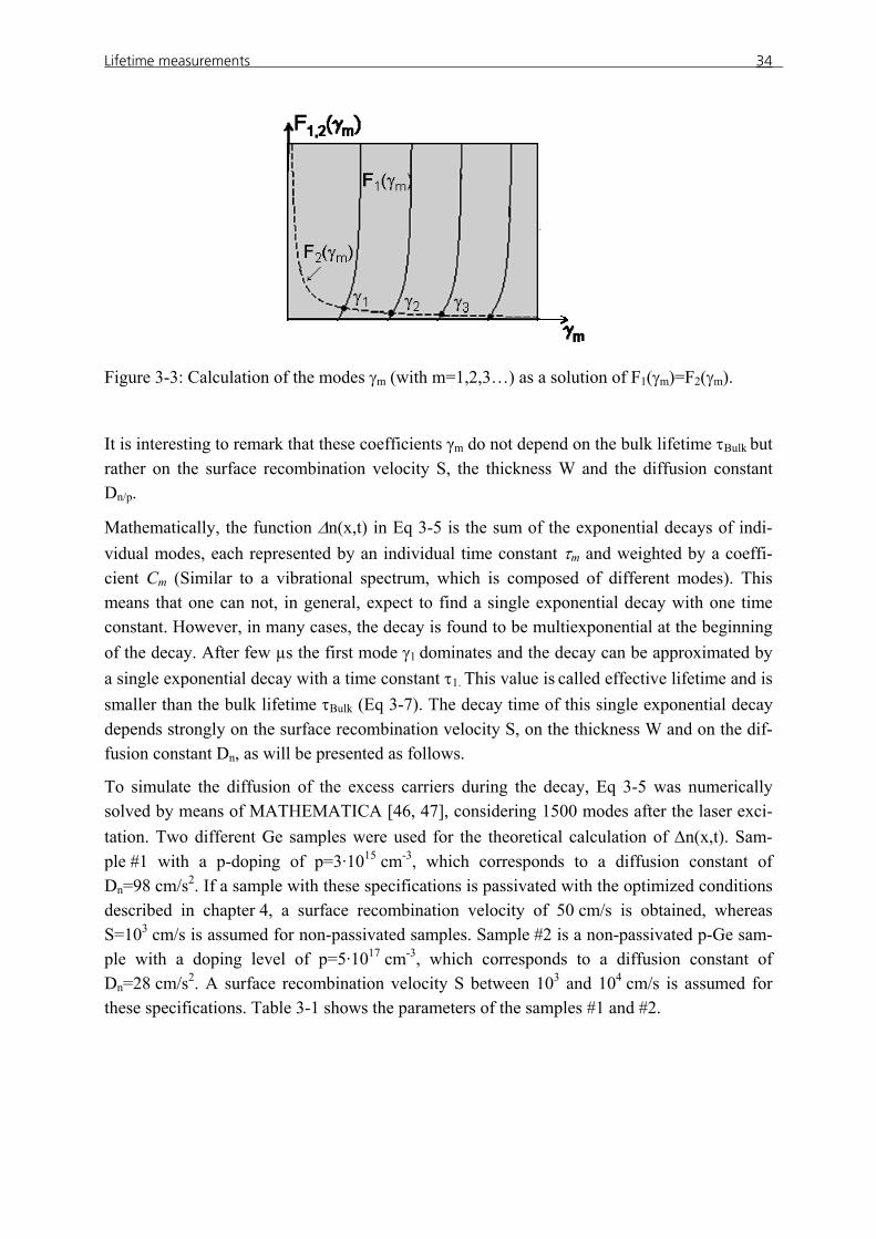
To simulate the diffusion of the excess carriers during the decay, Eq 3-5 was numerically solved by means of MATHEMATICA [46, 47], considering 1500 modes after the laser exci-tation. Two different Ge samples were used for the theoretical calculation of Δn(x,t). Sam-ple #1 with a p-doping of p=3·1015 cm-3, which corresponds to a diffusion constant of Dn=98 cm/s2. If a sample with these specifications is passivated with the optimized conditions described in chapter 4, a surface recombination velocity of 50 cm/s is obtained, whereas S=103 cm/s is assumed for non-passivated samples. Sample #2 is a non-passivated p-Ge sam-ple with a doping level of p=5·1017 cm-3, which corresponds to a diffusion constant of Dn=28 cm/s2. A surface recombination velocity S between 103 and 104 cm/s is assumed for these specifications. Table 3-1 shows the parameters of the samples #1 and #2.
Lifetime measurements
35
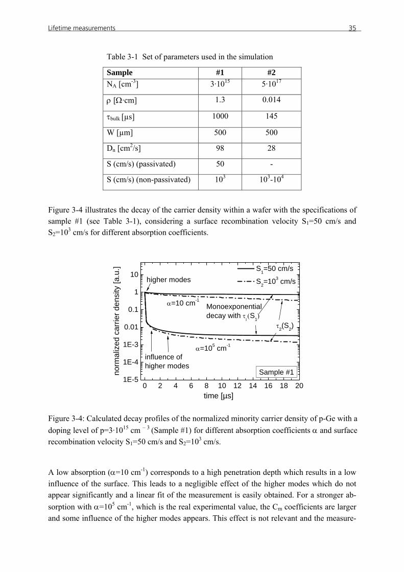
Table 3-1 Set of parameters used in the simulation
Sample #1 #2 NA [cm-3] 3·1015 5·1017
ρ [Ω·cm] 1.3 0.014
τbulk [µs] 1000 145
W [µm] 500 500
Dn [cm2/s] 98 28
S (cm/s) (passivated) 50 -
S (cm/s) (non-passivated) 103 103-104
Figure 3-4 illustrates the decay of the carrier density within a wafer with the specifications of sample #1 (see Table 3-1), considering a surface recombination velocity S1=50 cm/s and S2=103 cm/s for different absorption coefficients.
0 2 4 6 8 10 12 14 16 18 201E-5
1E-4
1E-3
0.01
0.1
1
10
τ2(S2)
influence of higher modes
α=105 cm-1
S1=50 cm/s
S2=103 cm/s
norm
aliz
ed c
arrie
r den
sity
[a.u
.]
time [µs]
α=10 cm-1
higher modes
Monoexponential decay with τ
1(S1)
Sample #1
Figure 3-4: Calculated decay profiles of the normalized minority carrier density of p-Ge with a doping level of p=3·1015 cm – 3 (Sample #1) for different absorption coefficients α and surface recombination velocity S1=50 cm/s and S2=103 cm/s.
A low absorption (α=10 cm-1) corresponds to a high penetration depth which results in a low influence of the surface. This leads to a negligible effect of the higher modes which do not appear significantly and a linear fit of the measurement is easily obtained. For a stronger ab-sorption with α=105 cm-1, which is the real experimental value, the Cm coefficients are larger and some influence of the higher modes appears. This effect is not relevant and the measure-
Lifetime measurements
36
ment can be approximated after a short time to a single exponential decay with a time con-stant τ1 and τ2. This evidently depends on the surface recombination velocity (τ1 for S1 and τ2
for S2).
0 2 4 6 8 10 12 14 16 18 201E-5
1E-4
1E-3
0.01
0.1
1
10
higher modesdominate
S=103 cm/s S=104 cm/s
norm
aliz
ed c
arrie
r den
sity
[a.u
.]
time [µs]
Monoexponential decay hard to see
α=105 cm-1
D=28 cm2/s
Sample #2
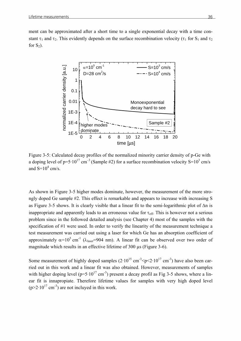
Figure 3-5: Calculated decay profiles of the normalized minority carrier density of p-Ge with a doping level of p=5·1017 cm–3 (Sample #2) for a surface recombination velocity S=103 cm/s and S=104 cm/s.
As shown in Figure 3-5 higher modes dominate, however, the measurement of the more stro-ngly doped Ge sample #2. This effect is remarkable and appears to increase with increasing S as Figure 3-5 shows. It is clearly visible that a linear fit to the semi-logarithmic plot of Δn is inappropriate and apparently leads to an erroneous value for τeff. This is however not a serious problem since in the followed detailed analysis (see Chapter 4) most of the samples with the specification of #1 were used. In order to verify the linearity of the measurement technique a test measurement was carried out using a laser for which Ge has an absorption coefficient of approximately α=105 cm-1 (λlaser=904 nm). A linear fit can be observed over two order of magnitude which results in an effective lifetime of 300 µs (Figure 3-6).
Some measurement of highly doped samples (2·1015 cm-3<p<2·1017 cm-3) have also been car-ried out in this work and a linear fit was also obtained. However, measurements of samples with higher doping level (p=5·1017 cm-3) present a decay profil as Fig 3-5 shows, where a lin-ear fit is innapropiate. Therefore lifetime values for samples with very high doped level (p>2·1017 cm-3) are not incluyed in this work.
Lifetime measurements
37
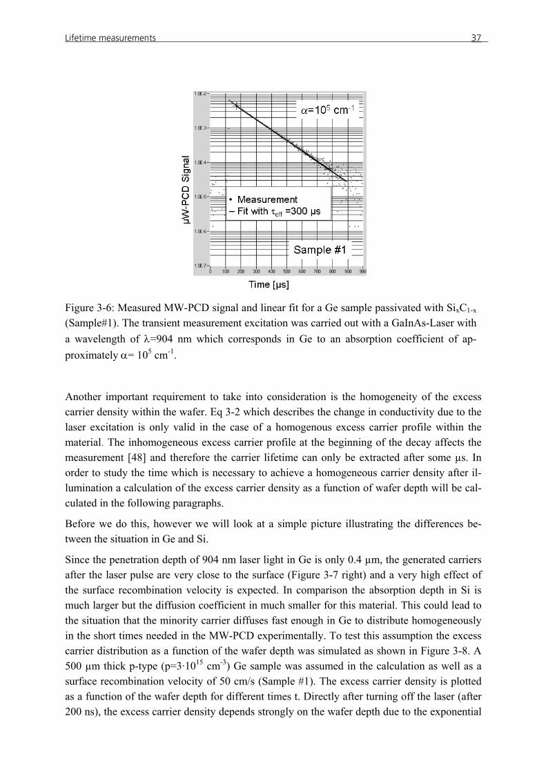
Figure 3-6: Measured MW-PCD signal and linear fit for a Ge sample passivated with SixC1-x (Sample#1). The transient measurement excitation was carried out with a GaInAs-Laser with a wavelength of λ=904 nm which corresponds in Ge to an absorption coefficient of ap-proximately α= 105 cm-1.
Another important requirement to take into consideration is the homogeneity of the excess carrier density within the wafer. Eq 3-2 which describes the change in conductivity due to the laser excitation is only valid in the case of a homogenous excess carrier profile within the material. The inhomogeneous excess carrier profile at the beginning of the decay affects the measurement [48] and therefore the carrier lifetime can only be extracted after some µs. In order to study the time which is necessary to achieve a homogeneous carrier density after il-lumination a calculation of the excess carrier density as a function of wafer depth will be cal-culated in the following paragraphs.
Before we do this, however we will look at a simple picture illustrating the differences be-tween the situation in Ge and Si.
Since the penetration depth of 904 nm laser light in Ge is only 0.4 µm, the generated carriers after the laser pulse are very close to the surface (Figure 3-7 right) and a very high effect of the surface recombination velocity is expected. In comparison the absorption depth in Si is much larger but the diffusion coefficient in much smaller for this material. This could lead to the situation that the minority carrier diffuses fast enough in Ge to distribute homogeneously in the short times needed in the MW-PCD experimentally. To test this assumption the excess carrier distribution as a function of the wafer depth was simulated as shown in Figure 3-8. A 500 µm thick p-type (p=3·1015 cm-3) Ge sample was assumed in the calculation as well as a surface recombination velocity of 50 cm/s (Sample #1). The excess carrier density is plotted as a function of the wafer depth for different times t. Directly after turning off the laser (after 200 ns), the excess carrier density depends strongly on the wafer depth due to the exponential
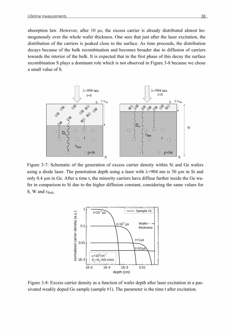
Lifetime measurements
38
absorption law. However, after 10 µs, the excess carrier is already distributed almost ho-mogenously over the whole wafer thickness. One sees that just after the laser excitation, the distribution of the carriers is peaked close to the surface. As time proceeds, the distribution decays because of the bulk recombination and becomes broader due to diffusion of carriers towards the interior of the bulk. It is expected that in the first phase of this decay the surface recombination S plays a dominant role which is not observed in Figure 3-8 because we chose a small value of S.
Figure 3-7: Schematic of the generation of excess carrier density within Si and Ge wafers using a diode laser. The penetration depth using a laser with λ=904 nm is 50 µm in Si and only 0.4 µm in Ge. After a time t, the minority carriers have diffuse farther inside the Ge wa-fer in comparison to Si due to the higher diffusion constant, considering the same values for S, W and τBulk.
1E-5 1E-4 1E-3 0.01
1E-3
0.01
0.1
1
Wafer thickness
Sample #1
t=1 µs
t=10 µs
t=10-2 µs
t=10-4 µs
α=105cm-1
S1=S2=50 cm/snorm
aliz
ed c
arrie
r den
sity
(a.u
.)
depth (cm)
Figure 3-8: Excess carrier density as a function of wafer depth after laser excitation in a pas-sivated weakly doped Ge sample (sample #1). The parameter is the time t after excitation.
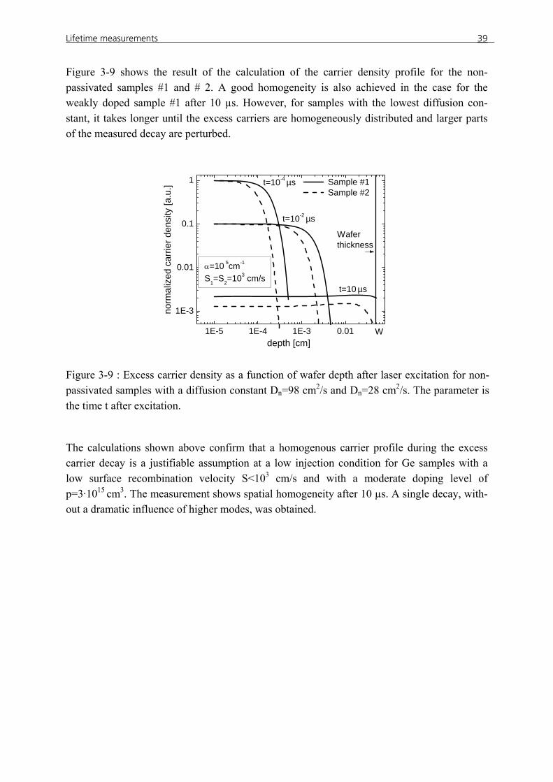
Lifetime measurements
39
Figure 3-9 shows the result of the calculation of the carrier density profile for the non-passivated samples #1 and # 2. A good homogeneity is also achieved in the case for the weakly doped sample #1 after 10 µs. However, for samples with the lowest diffusion con-stant, it takes longer until the excess carriers are homogeneously distributed and larger parts of the measured decay are perturbed.
1E-5 1E-4 1E-3 0.01
1E-3
0.01
0.1
1
t=10 µs
t=10-2 µs
α=10 5cm-1
S1=S2=103 cm/s
Sample #1 Sample #2
norm
aliz
ed c
arrie
r den
sity
[a.u
.]
depth [cm]
t=10-4 µs
W
Wafer thickness
Figure 3-9 : Excess carrier density as a function of wafer depth after laser excitation for non-passivated samples with a diffusion constant Dn=98 cm2/s and Dn=28 cm2/s. The parameter is the time t after excitation.
The calculations shown above confirm that a homogenous carrier profile during the excess carrier decay is a justifiable assumption at a low injection condition for Ge samples with a low surface recombination velocity S<103 cm/s and with a moderate doping level of p=3·1015 cm3. The measurement shows spatial homogeneity after 10 µs. A single decay, with-out a dramatic influence of higher modes, was obtained.
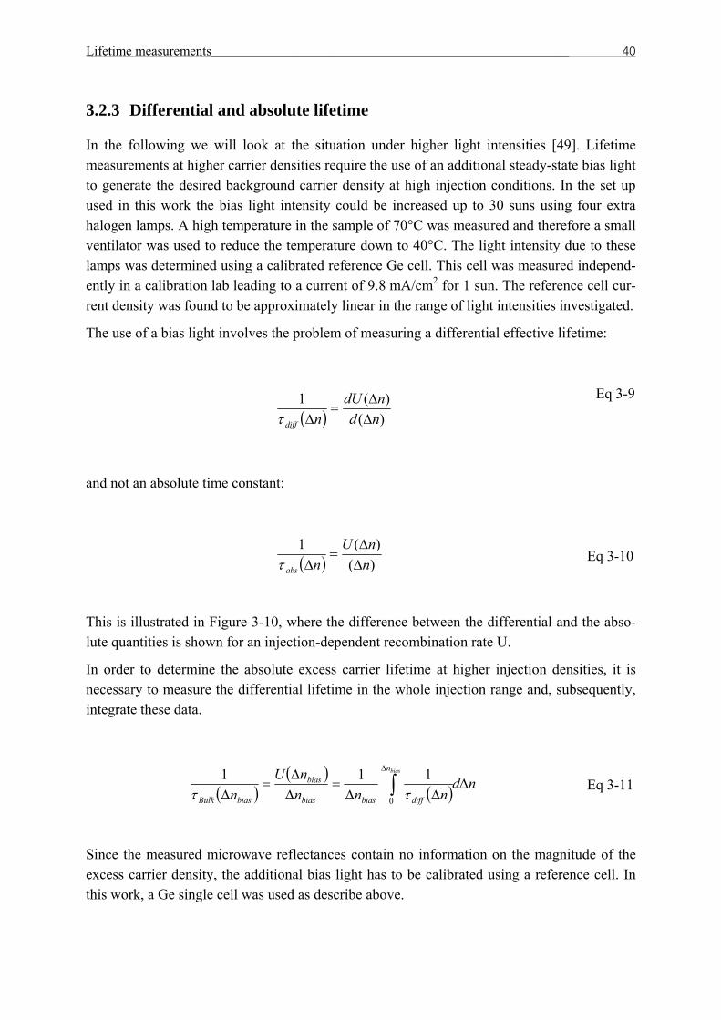
Lifetime measurements___________________________________________________________ 40
3.2.3 Differential and absolute lifetime
In the following we will look at the situation under higher light intensities [49]. Lifetime measurements at higher carrier densities require the use of an additional steady-state bias light to generate the desired background carrier density at high injection conditions. In the set up used in this work the bias light intensity could be increased up to 30 suns using four extra halogen lamps. A high temperature in the sample of 70°C was measured and therefore a small ventilator was used to reduce the temperature down to 40°C. The light intensity due to these lamps was determined using a calibrated reference Ge cell. This cell was measured independ-ently in a calibration lab leading to a current of 9.8 mA/cm2 for 1 sun. The reference cell cur-rent density was found to be approximately linear in the range of light intensities investigated.
The use of a bias light involves the problem of measuring a differential effective lifetime:
( ) )()(1
ndndU
ndiff ΔΔ
=Δτ
Eq 3-9
and not an absolute time constant:
( ) )()(1
nnU
nabs ΔΔ
=Δτ
Eq 3-10
This is illustrated in Figure 3-10, where the difference between the differential and the abso-lute quantities is shown for an injection-dependent recombination rate U.
In order to determine the absolute excess carrier lifetime at higher injection densities, it is necessary to measure the differential lifetime in the whole injection range and, subsequently, integrate these data.
( )( )
( ) ndnnn
nUn
biasn
diffbiasbias
bias
biasBulk
ΔΔΔ
=ΔΔ
=Δ ∫
Δ
0
111ττ
Eq 3-11
Since the measured microwave reflectances contain no information on the magnitude of the excess carrier density, the additional bias light has to be calibrated using a reference cell. In this work, a Ge single cell was used as describe above.
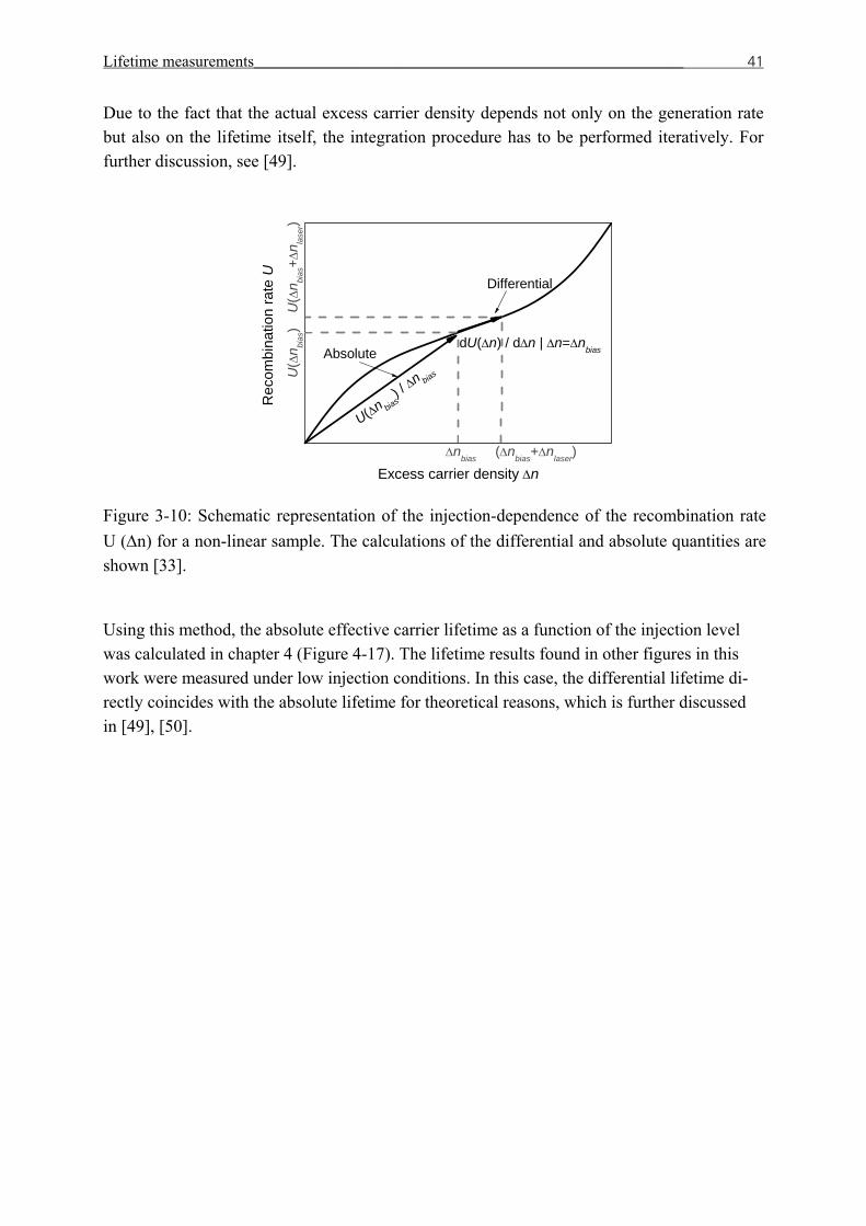
Lifetime measurements___________________________________________________________ 41
Due to the fact that the actual excess carrier density depends not only on the generation rate but also on the lifetime itself, the integration procedure has to be performed iteratively. For further discussion, see [49].
Absolute
U(Δn bias) /
Δn biasU(Δ
n bias
) U
(Δn bi
as+Δ
n lase
r)
Rec
ombi
natio
n ra
te U
Excess carrier density ΔnΔnbias (Δnbias+Δnlaser)
dU(Δn) / dΔn | Δn=Δnbias
Differential
Figure 3-10: Schematic representation of the injection-dependence of the recombination rate U (Δn) for a non-linear sample. The calculations of the differential and absolute quantities are shown [33].
Using this method, the absolute effective carrier lifetime as a function of the injection level was calculated in chapter 4 (Figure 4-17). The lifetime results found in other figures in this work were measured under low injection conditions. In this case, the differential lifetime di-rectly coincides with the absolute lifetime for theoretical reasons, which is further discussed in [49], [50].

Lifetime measurements___________________________________________________________ 42
Ge surface passivation___________________________________________________________ 43
4 Ge surface passivation
In this chapter the process to obtain a suitable passivation for Ge surfaces will
be described. The effectiveness of the passivation will be characterized by
measurement of the effective minority carrier lifetime using MW-PCD. A very
low surface recombination velocity of 50 cm/s is achieved for samples with a
doping level of 3·1015 cm-3. Under this condition it is possible to find out spe-
cific material constants of Ge which, until now, have not been well known like
intrinsic recombination parameters and bulk lifetime as a function of the dop-
ing level. Finally a brief discussion of the possible passivation mechanisms will
be presented.
4.1 Introduction
One of the most important prerequisites to improving the electrical quality of a photovoltaic cell is the passivation of its surfaces. While Si conform an extremely high-quality stable di-electric SiO2 that can be used for surface passivation, Ge surfaces are not effectively pas-sivated with Ge oxides which are water soluble and therefore rather unstable in air. A process to passivate Ge surfaces has been developed in this work and is discussed in detail in this sec-tion. Solar cells described in chapter 5 and 6 are provided with front and back side passivation layers using the optimized parameters described in this chapter.
First a brief discussion about the fundamentals of surface passivation will be presented. Sec-ond an overview of the passivation used in Ge is given.
4.1.1 Fundamentals of surface passivation
The surface of a semiconductor represents a large disturbance of the crystal lattice. Non-saturated covalent electron states lead to dangling bonds which introduce large defect states in the energy gap, which are frequently recombination active. As discussed before, the recombi-nation via defects is described by the Shockley-Read-Hall (SRH) theory.
A simple model has been presented for the recombination effect at the surface of a solar cell (see Figure 4-1 left). Excess charge carriers photo-generated close to the surface, as indicated can recombine at the many active defects (thick horizontal lines) which results in a high re-combination rate USurface. Excess carrier generated in the bulk can recombine at some bulk defects (bulk recombination) or diffuse to the surface and recombine there as indicated [25].
There are two mechanisms that allow reduction in surface recombination:
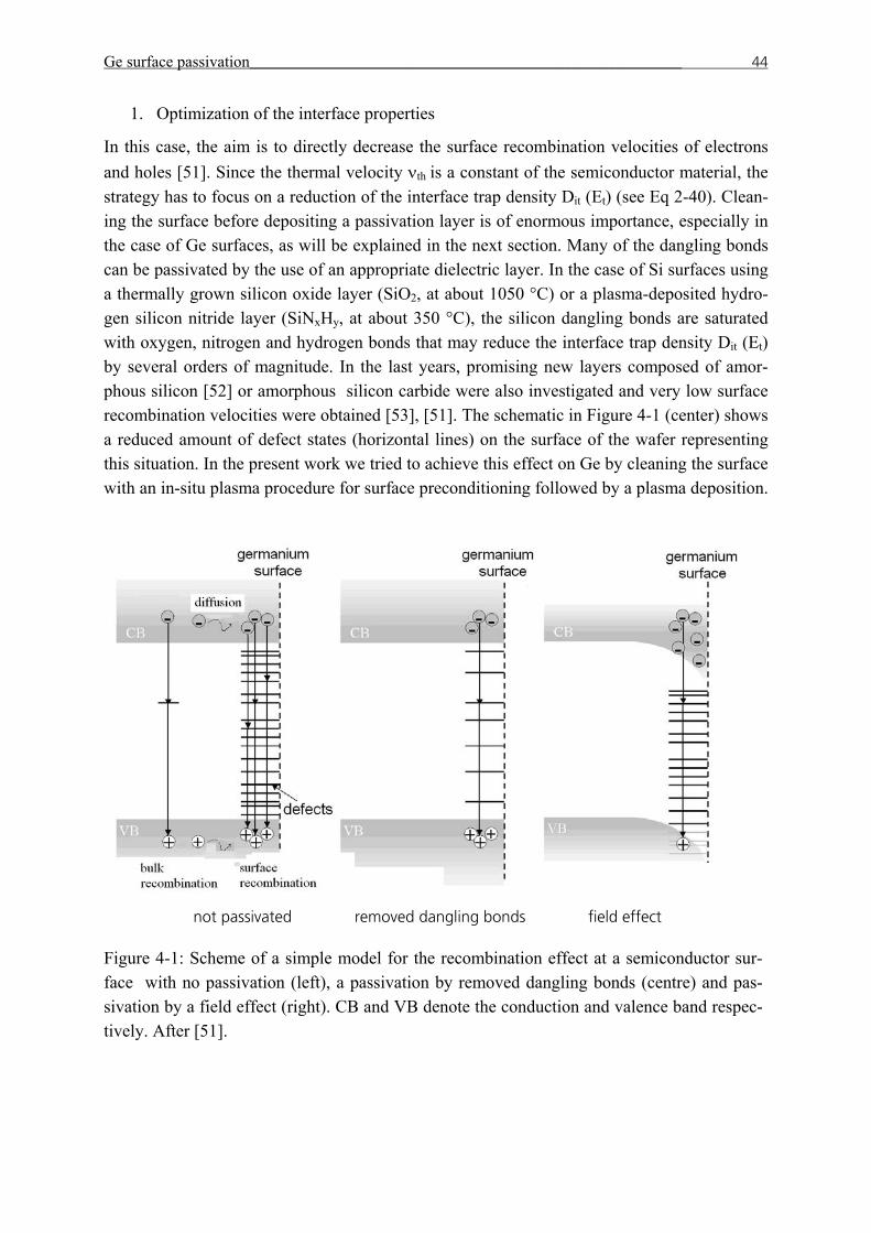
Ge surface passivation___________________________________________________________ 44
1. Optimization of the interface properties
In this case, the aim is to directly decrease the surface recombination velocities of electrons and holes [51]. Since the thermal velocity νth is a constant of the semiconductor material, the strategy has to focus on a reduction of the interface trap density Dit (Et) (see Eq 2-40). Clean-ing the surface before depositing a passivation layer is of enormous importance, especially in the case of Ge surfaces, as will be explained in the next section. Many of the dangling bonds can be passivated by the use of an appropriate dielectric layer. In the case of Si surfaces using a thermally grown silicon oxide layer (SiO2, at about 1050 °C) or a plasma-deposited hydro-gen silicon nitride layer (SiNxHy, at about 350 °C), the silicon dangling bonds are saturated with oxygen, nitrogen and hydrogen bonds that may reduce the interface trap density Dit (Et) by several orders of magnitude. In the last years, promising new layers composed of amor-phous silicon [52] or amorphous silicon carbide were also investigated and very low surface recombination velocities were obtained [53], [51]. The schematic in Figure 4-1 (center) shows a reduced amount of defect states (horizontal lines) on the surface of the wafer representing this situation. In the present work we tried to achieve this effect on Ge by cleaning the surface with an in-situ plasma procedure for surface preconditioning followed by a plasma deposition.
not passivated removed dangling bonds field effect
Figure 4-1: Scheme of a simple model for the recombination effect at a semiconductor sur-face with no passivation (left), a passivation by removed dangling bonds (centre) and pas-sivation by a field effect (right). CB and VB denote the conduction and valence band respec-tively. After [51].
Ge surface passivation___________________________________________________________ 45
2. Reduction of the surface concentration of electrons and holes
The second approach to decrease the recombination rate is to reduce the relevant minority carrier concentration at the surface. This can be achieved in an n-type semiconductor by repel-ling the minority holes from the surface by a positive charge in the surface dielectric (not shown in Figure 4-1). Technologically, this may be achieved in two different ways:
- Formation of a back surface field (BSF): The incorporation of an additional doping profile forming a high-low-junction (n+n or p+p) which repels the minority carriers from the surface. Alloyed aluminium is used for this purpose in p-type Si.
- Field effect passivation: Fixed charges in an overlying dielectric layer establish an electrical field at the surface of the semiconductor (band bending) that repel minority carriers. This effect appears in n-type Si surfaces using for example SiNx passivation layers which exhibit fixed positive charges [25, 54].
State of the art of Ge passivation will be described in the following section.
4.1.2 State of the art passivation layers for Ge surfaces
Passivation of Ge has not been as extensively investigated as for Si. As already pointed out, one of the disadvantages of Ge in comparison to Si is the instability of the native oxide. A crucial point concerning the passivation of Ge surfaces is the removal of the native oxide since GexOy is hygroscopic and its instability seriously enhances surface recombination.
Hymes and Rosenberg et al. studied the use of Ge oxy-nitride (Ge2N2O) formed by oxidation and subsequent nitridation using ammonia at 600 °C [55]. This process results in the forma-tion of a stable Ge2N2O with high interfacial quality for MOS and junction passivation appli-cations. Another promising Ge surface passivation treatment consists in depositing an ultra thin Si epitaxial interlayer, followed by its chemical or thermal oxidation [21]. In the epitaxial reactor, the Ge wafer is baked in H2 at a typical temperature of 600-650°C in order to obtain a clean Ge surface. An ultra thin Si epitaxial layer is deposited on the Ge surface using SiH4 at a typical temperature of 500 °C. Subsequently the wafers were transfered to another chamber for the metal organic chemical vapour deposition (MOCVD) of HfO2. High-resolution cross sectional TEM shows the image of the Ge/Si/GeOx/HfO2 gate stack. Si fully covers the Ge surface and is kept monolayer range at the same time. Ge remains un-oxidized after the Si passivation and the formation of Ge oxide was greatly suppressed during the HfO2. These both processes seem to be very efficient in order to passivate Ge surfaces due to the very good current-voltage and capacitor-voltage characteristics results in the microelectronic devices [21], unfortunately such high temperature are not preferably for solar cell technology and al-ternatives which allow lower temperature in the procedure are desirable.
Nagashima et al used plasma enhanced chemical vapour deposition (PECVD) silicon nitride for surface passivation of stand alone Ge TPV photovoltaic cells. Using this material a voltage of 197 mV has been achieved [34]. Wang et al [56] reported a reduction in interface state den-sity using a very thin layer of amorphous silicon in combination with SiO2 to passivate Ge. Posthuma et al. [34] have recently combined a wet-chemical treatment with subsequent in-situ
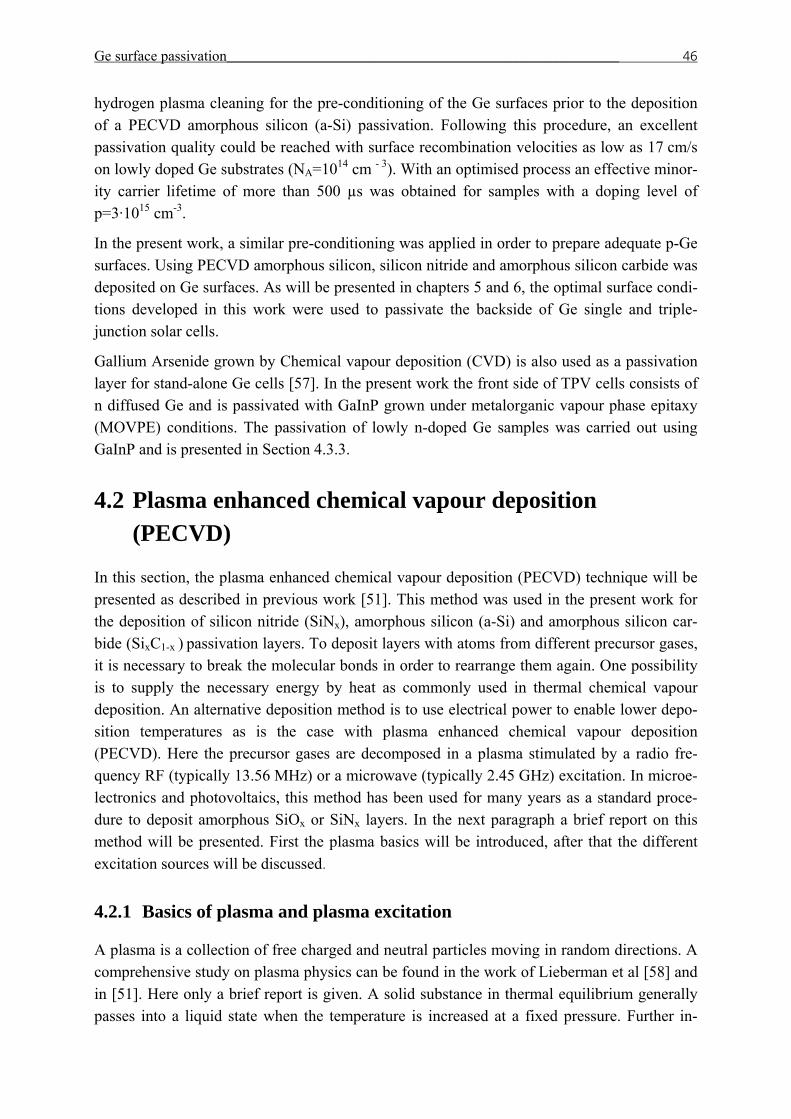
Ge surface passivation___________________________________________________________ 46
hydrogen plasma cleaning for the pre-conditioning of the Ge surfaces prior to the deposition of a PECVD amorphous silicon (a-Si) passivation. Following this procedure, an excellent passivation quality could be reached with surface recombination velocities as low as 17 cm/s on lowly doped Ge substrates (NA=1014 cm - 3). With an optimised process an effective minor-ity carrier lifetime of more than 500 µs was obtained for samples with a doping level of p=3·1015 cm-3.
In the present work, a similar pre-conditioning was applied in order to prepare adequate p-Ge surfaces. Using PECVD amorphous silicon, silicon nitride and amorphous silicon carbide was deposited on Ge surfaces. As will be presented in chapters 5 and 6, the optimal surface condi-tions developed in this work were used to passivate the backside of Ge single and triple-junction solar cells.
Gallium Arsenide grown by Chemical vapour deposition (CVD) is also used as a passivation layer for stand-alone Ge cells [57]. In the present work the front side of TPV cells consists of n diffused Ge and is passivated with GaInP grown under metalorganic vapour phase epitaxy (MOVPE) conditions. The passivation of lowly n-doped Ge samples was carried out using GaInP and is presented in Section 4.3.3.
4.2 Plasma enhanced chemical vapour deposition (PECVD)
In this section, the plasma enhanced chemical vapour deposition (PECVD) technique will be presented as described in previous work [51]. This method was used in the present work for the deposition of silicon nitride (SiNx), amorphous silicon (a-Si) and amorphous silicon car-bide (SixC1-x ) passivation layers. To deposit layers with atoms from different precursor gases, it is necessary to break the molecular bonds in order to rearrange them again. One possibility is to supply the necessary energy by heat as commonly used in thermal chemical vapour deposition. An alternative deposition method is to use electrical power to enable lower depo-sition temperatures as is the case with plasma enhanced chemical vapour deposition (PECVD). Here the precursor gases are decomposed in a plasma stimulated by a radio fre-quency RF (typically 13.56 MHz) or a microwave (typically 2.45 GHz) excitation. In microe-lectronics and photovoltaics, this method has been used for many years as a standard proce-dure to deposit amorphous SiOx or SiNx layers. In the next paragraph a brief report on this method will be presented. First the plasma basics will be introduced, after that the different excitation sources will be discussed.
4.2.1 Basics of plasma and plasma excitation
A plasma is a collection of free charged and neutral particles moving in random directions. A comprehensive study on plasma physics can be found in the work of Lieberman et al [58] and in [51]. Here only a brief report is given. A solid substance in thermal equilibrium generally passes into a liquid state when the temperature is increased at a fixed pressure. Further in-
Ge surface passivation___________________________________________________________ 47
crease leads to the gas phase of the substance. At a sufficiently high temperature, the mole-cules in the gas decompose to form a gas of atoms that move freely in random directions. If the temperature is further increased, the atoms decompose into freely moving charged parti-cles (electrons and positive ions) and the substance enters the plasma state. The presence of free charge particles makes the plasma electrically conductive which leads to different electri-cal properties as in solids, liquids or gases. For this reason plasmas are often called the fourth state of matter.
To achieve the plasma state particles need energy for the dissociation and ionisation. The dif-ferent methods of plasma excitation will be discussed in the next. First the creation of the sheaths and the plasma ionization process will be clarified.
It is important to note that the electron thermal velocity is at least 100 times the ion thermal velocity [58]. Consider a plasma of width l with charged particle density ne=ni (e subscript for electron and i subscript for ion) initially confined between two grounded absorbing walls. The electric potential Φ and the electric field Ex is zero everywhere because the net charge density ρ=e (ni-ne) is zero. On a very small time scale however some of the fast moving electrons are lost near the walls (see on the right hand). The net positive ρ within the sheaths leads to a po-tential profile that is positive within the plasma and falls to zero near the walls. This acts as a confining valley potential for the electrons and a hill for the ions because the electron fields within the sheaths point from the plasma to the wall. Thus the force acting on electrons is di-rected into the plasma and the ions that enter the sheaths are accelerated into the walls.
Figure 4-2: The formation of plasma sheaths. (a) Initial ion and electron densities and poten-tial. (b) Densities, electric field, and potential after formation of the sheath. [58]
In this work two different methods of plasma excitation were used. The radio frequency (RF) and the microwave (MW). In principle they differ in the excitation sources which work at different frequencies and can achieve different plasma states.
Ge surface passivation___________________________________________________________ 48
4.2.1.1 Radio frequency plasma
The main setup can be described as a vacuum chamber containing two planar electrodes sepa-rated by a spacing l and driven by a RF power source. The substrates are placed on one elec-trode, feedstock gases are admitted to flow through the discharge, and effluent gases are re-moved by the vacuum pump (see Figure 4-3, left hand side). The operation of capacitive by driven discharges is reasonably well understood. The distribution of the electrons and ions is not homogeneous. The mobile plasma electrons oscillate back and forth within the space cloud of ions. The massive ions contrary respond only to the time average electric fields. As explained before oscillation of the electron cloud created sheath regions near each electrode that contain net positive charge when average over one oscillation period. This excess pro-duces a strong time average electric field within each sheath directed from the plasma to the electrode. Ions flowing within the bulk plasma near the centre of the discharge can be acceler-ated by the sheath to high energies as they flow to the substrates, leading to energetic-ion en-hanced processes.
4.2.1.2 Microwave plasma
In microwave plasmas the needed energy is introduced to the reactor via electromagnetic waves as in the case of RF plasmas but with a much higher frequency. This leads to the case that the electrons are much more immobile and less charging of surfaces occurs. Also higher plasma densities can be obtained. A review on microwave discharges is found in the work of Rentsch [59]. Figure 4-3 on the right exhibits a schematic cross section of the plasma zone in a reactor with an antenna (inner conductor) and a quartz tube surrounding it and protecting it from the process gases. The magnets on the left and right side are densifying the plasma. Process gases can enter the reactor from the top (close to the plasma source) or from the sides (close to the substrates). The microwave power is injected into the linear antenna from both sides using two microwave generators. It is important to remark here that this is only an ex-ample of microwave plasma excitation and there is a high variety of it depending on the reac-tor geometry and specification. In plasma reactor AK400 the energy is coupled to the plasma by microwaves generated by two copper antennas inside two quartz tubes whereas plasma SI uses a remote microwave. A detailed explanation can be found in [60].
In Figure 4-4, an overview of the possible processes in the plasma during deposition and etch-ing processes is presented. Two important regions, the gas-phase and the surface, are outlined. Even this simplified sketch shows the complexity of reaction mechanisms in the plasma. In the gas-phase, both ionization and dissociation are carried out. In the surface region, many different reactions compete with each other. Therefore a small change in a process parameter may be decisive regarding deposition or etching characteristics of the process.
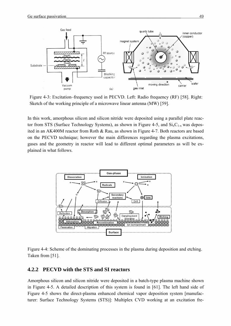
Ge surface passivation___________________________________________________________ 49
Figure 4-3: Excitation–frequency used in PECVD. Left: Radio frequency (RF) [58]. Right: Sketch of the working principle of a microwave linear antenna (MW) [59].
In this work, amorphous silicon and silicon nitride were deposited using a parallel plate reac-tor from STS (Surface Technology Systems), as shown in Figure 4-5, and SixC1-x was depos-ited in an AK400M reactor from Roth & Rau, as shown in Figure 4-7. Both reactors are based on the PECVD technique; however the main differences regarding the plasma excitations, gases and the geometry in reactor will lead to different optimal parameters as will be ex-plained in what follows.
Figure 4-4: Scheme of the dominating processes in the plasma during deposition and etching. Taken from [51].
4.2.2 PECVD with the STS and SI reactors
Amorphous silicon and silicon nitride were deposited in a batch-type plasma machine shown in Figure 4-5. A detailed description of this system is found in [61]. The left hand side of Figure 4-5 shows the direct-plasma enhanced chemical vapor deposition system [manufac-turer: Surface Technology Systems (STS)]: Multiplex CVD working at an excitation fre-
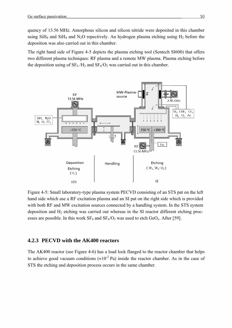
Ge surface passivation___________________________________________________________ 50
quency of 13.56 MHz. Amorphous silicon and silicon nitride were deposited in this chamber using SiH4 and SiH4 and N2O repectively. An hydrogen plasma etching using H2 before the deposition was also carried out in this chamber.
The right hand side of Figure 4-5 depicts the plasma etching tool (Sentech SI600) that offers two different plasma techniques: RF plasma and a remote MW plasma. Plasma etching before the deposition using of SF6 /H2 and SF6/O2 was carried out in this chamber.
Figure 4-5: Small laboratory-type plasma system PECVD consisting of an STS pat on the left hand side which use a RF excitation plasma and an SI pat on the right side which is provided with both RF and MW excitation sources connected by a handling system. In the STS system deposition and H2 etching was carried out whereas in the SI reactor different etching proc-esses are possible. In this work SF6 and SF6/O2 was used to etch GeOx. After [59].
4.2.3 PECVD with the AK400 reactors
The AK400 reactor (see Figure 4-6) has a load lock flanged to the reactor chamber that helps to achieve good vacuum conditions (≈10-2 Pa) inside the reactor chamber. As in the case of STS the etching and deposition process occurs in the same chamber.
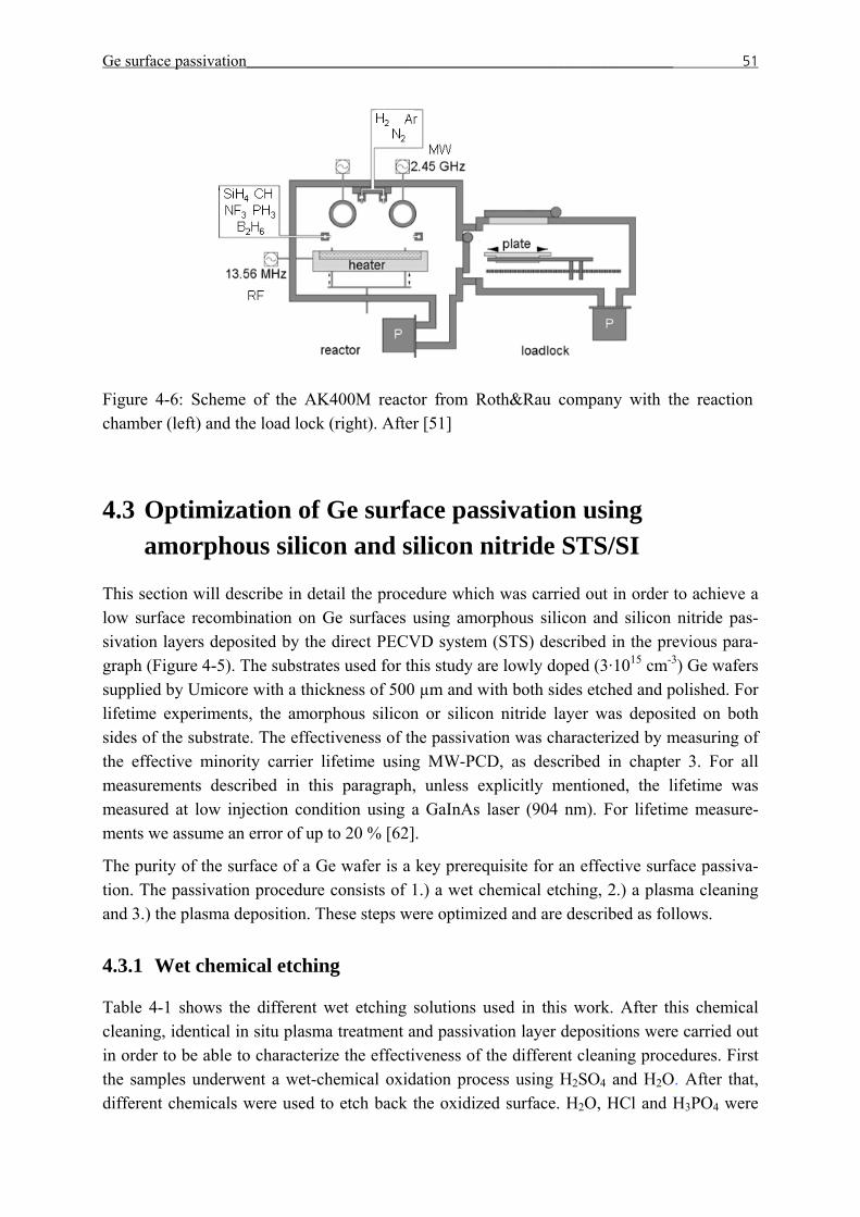
Ge surface passivation___________________________________________________________ 51
Figure 4-6: Scheme of the AK400M reactor from Roth&Rau company with the reaction chamber (left) and the load lock (right). After [51]
4.3 Optimization of Ge surface passivation using amorphous silicon and silicon nitride STS/SI
This section will describe in detail the procedure which was carried out in order to achieve a low surface recombination on Ge surfaces using amorphous silicon and silicon nitride pas-sivation layers deposited by the direct PECVD system (STS) described in the previous para-graph (Figure 4-5). The substrates used for this study are lowly doped (3·1015 cm-3) Ge wafers supplied by Umicore with a thickness of 500 µm and with both sides etched and polished. For lifetime experiments, the amorphous silicon or silicon nitride layer was deposited on both sides of the substrate. The effectiveness of the passivation was characterized by measuring of the effective minority carrier lifetime using MW-PCD, as described in chapter 3. For all measurements described in this paragraph, unless explicitly mentioned, the lifetime was measured at low injection condition using a GaInAs laser (904 nm). For lifetime measure-ments we assume an error of up to 20 % [62].
The purity of the surface of a Ge wafer is a key prerequisite for an effective surface passiva-tion. The passivation procedure consists of 1.) a wet chemical etching, 2.) a plasma cleaning and 3.) the plasma deposition. These steps were optimized and are described as follows.
4.3.1 Wet chemical etching
Table 4-1 shows the different wet etching solutions used in this work. After this chemical cleaning, identical in situ plasma treatment and passivation layer depositions were carried out in order to be able to characterize the effectiveness of the different cleaning procedures. First the samples underwent a wet-chemical oxidation process using H2SO4 and H2O. After that, different chemicals were used to etch back the oxidized surface. H2O, HCl and H3PO4 were
Ge surface passivation___________________________________________________________ 52
used for this purpose. The best results were achieved for a wet etching solution consisting of a wet chemical sequence of 10 sec H2SO4 at 60 °C and 10 min H3PO4 etch combined with a subsequent rinsing in deionised water. Lifetimes of 400 ± 80 µs were obtained (see Table
4-1). A HF treatment after this process has shown not to give better results. Besides, a HF treatment leaves a rough surface which is not desirable [63].
After this pre-conditioning, the samples were stored for one day under clean-room conditions to allow a reproducible oxidation of the surface. It was found that this step was necessary to avoid undefined surface conditions of the samples depending on the interval between the wet chemical treatment and subsequent processing. In this way, a reasonable comparison and analysis of the passivation quality of different Ge samples could be assured.
Table 4-1 Effective lifetime measurements on Ge samples with a doping level of 3·1015 cm-3 and a thickness of 500 µm obtained after a chemical ex situ cleaning procedure followed by an optimized plasma etching and plasma deposition treatment.
Cleaning condition after 10 s H2SO4 at 60 °C
Lifetime [µs]
No more treatment 130±26
10 min H2O 300±60
10 min HCl 350±70
10 min H3PO4 400±80
10 min H3PO4 / 5 min HF 300±60
4.3.2 Plasma cleaning
After the chemical etching, the native oxide formed during air exposure of Ge was removed by a dry etching step under vacuum conditions inside the PECVD reactor. Different plasma etching conditions were investigated and are shown in Table 4-2. Using an SF6 and H2/Ar gas mixture for the plasma etch process in the SI reactor (Figure 4-5 right) followed by the depo-sition of the passivation layer in the STS reactor (Figure 4-5 left), an excellent passivation was achieved. Unfortunately, these results were not reproducible. A possible explanation for this could be the oxidation during the transport from the SI to the STS reactor in perhapd in-sufficiently high vacuum. Using SF6 and O2 as reactive gases, only very low lifetimes of 8±1 µs were measured. Oxygen is probably responsible for an inappropriate surface prepara-tion which leads to a very high surface recombination velocity.
Samples that were exposed to a H2 plasma in the STS chamber show a better reproducibility probably because both surface pre-conditioning and deposition of the passivation layer are carried out in the same reactor (STS).
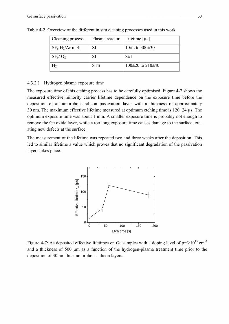
Ge surface passivation___________________________________________________________ 53
Table 4-2 Overview of the different in situ cleaning processes used in this work
Cleaning process Plasma reactor Lifetime [µs]
SF6 H2/Ar in SI SI 10±2 to 300±30
SF6/ O2 SI 8±1
H2 STS 100±20 to 210±40
4.3.2.1 Hydrogen plasma exposure time
The exposure time of this etching process has to be carefully optimised. Figure 4-7 shows the measured effective minority carrier lifetime dependence on the exposure time before the deposition of an amorphous silicon passivation layer with a thickness of approximately 30 nm. The maximum effective lifetime measured at optimum etching time is 120±24 µs. The optimum exposure time was about 1 min. A smaller exposure time is probably not enough to remove the Ge oxide layer, while a too long exposure time causes damage to the surface, cre-ating new defects at the surface.
The measurement of the lifetime was repeated two and three weeks after the deposition. This led to similar lifetime a value which proves that no significant degradation of the passivation layers takes place.
0 50 100 150 2000
50
100
150
Effe
ctiv
e lif
etim
e τ ef
f [µs]
Etch time [s]
Figure 4-7: As deposited effective lifetimes on Ge samples with a doping level of p=3·1015 cm-3 and a thickness of 500 µm as a function of the hydrogen-plasma treatment time prior to the deposition of 30 nm thick amorphous silicon layers.
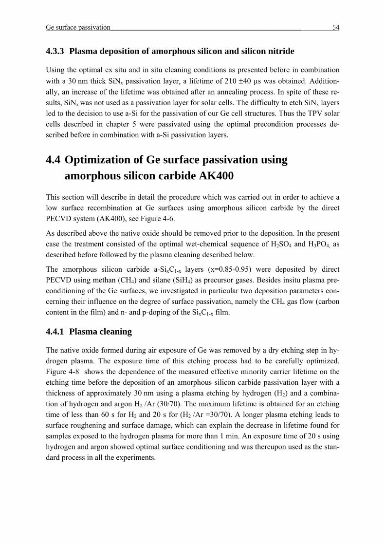
Ge surface passivation___________________________________________________________ 54
4.3.3 Plasma deposition of amorphous silicon and silicon nitride
Using the optimal ex situ and in situ cleaning conditions as presented before in combination with a 30 nm thick SiNx passivation layer, a lifetime of 210 ±40 µs was obtained. Addition-ally, an increase of the lifetime was obtained after an annealing process. In spite of these re-sults, SiNx was not used as a passivation layer for solar cells. The difficulty to etch SiNx layers led to the decision to use a-Si for the passivation of our Ge cell structures. Thus the TPV solar cells described in chapter 5 were passivated using the optimal precondition processes de-scribed before in combination with a-Si passivation layers.
4.4 Optimization of Ge surface passivation using amorphous silicon carbide AK400
This section will describe in detail the procedure which was carried out in order to achieve a low surface recombination at Ge surfaces using amorphous silicon carbide by the direct PECVD system (AK400), see Figure 4-6.
As described above the native oxide should be removed prior to the deposition. In the present case the treatment consisted of the optimal wet-chemical sequence of H2SO4 and H3PO4, as described before followed by the plasma cleaning described below.
The amorphous silicon carbide a-SixC1-x layers (x=0.85-0.95) were deposited by direct PECVD using methan (CH4) and silane (SiH4) as precursor gases. Besides insitu plasma pre-conditioning of the Ge surfaces, we investigated in particular two deposition parameters con-cerning their influence on the degree of surface passivation, namely the CH4 gas flow (carbon content in the film) and n- and p-doping of the SixC1-x film.
4.4.1 Plasma cleaning
The native oxide formed during air exposure of Ge was removed by a dry etching step in hy-drogen plasma. The exposure time of this etching process had to be carefully optimized. Figure 4-8 shows the dependence of the measured effective minority carrier lifetime on the etching time before the deposition of an amorphous silicon carbide passivation layer with a thickness of approximately 30 nm using a plasma etching by hydrogen (H2) and a combina-tion of hydrogen and argon H2 /Ar (30/70). The maximum lifetime is obtained for an etching time of less than 60 s for H2 and 20 s for (H2 /Ar =30/70). A longer plasma etching leads to surface roughening and surface damage, which can explain the decrease in lifetime found for samples exposed to the hydrogen plasma for more than 1 min. An exposure time of 20 s using hydrogen and argon showed optimal surface conditioning and was thereupon used as the stan-dard process in all the experiments.
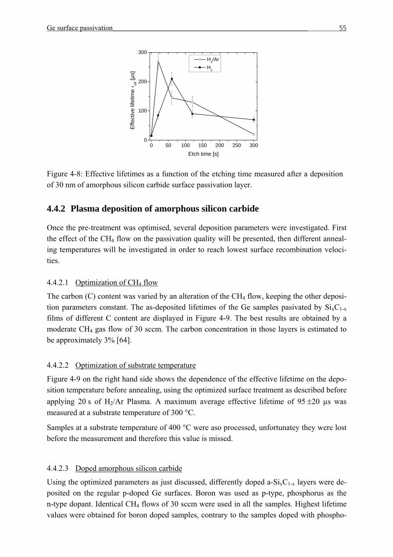
Ge surface passivation___________________________________________________________ 55
0 50 100 150 200 250 3000
100
200
300
Effe
ctiv
e lif
etim
e τ ef
f [µs]
Etch time [s]
H2/Ar H2
Figure 4-8: Effective lifetimes as a function of the etching time measured after a deposition of 30 nm of amorphous silicon carbide surface passivation layer.
4.4.2 Plasma deposition of amorphous silicon carbide
Once the pre-treatment was optimised, several deposition parameters were investigated. First the effect of the CH4 flow on the passivation quality will be presented, then different anneal-ing temperatures will be investigated in order to reach lowest surface recombination veloci-ties. 4.4.2.1 Optimization of CH4 flow
The carbon (C) content was varied by an alteration of the CH4 flow, keeping the other deposi-tion parameters constant. The as-deposited lifetimes of the Ge samples pasivated by SixC1-x films of different C content are displayed in Figure 4-9. The best results are obtained by a moderate CH4 gas flow of 30 sccm. The carbon concentration in those layers is estimated to be approximately 3% [64].
4.4.2.2 Optimization of substrate temperature
Figure 4-9 on the right hand side shows the dependence of the effective lifetime on the depo-sition temperature before annealing, using the optimized surface treatment as described before applying 20 s of H2/Ar Plasma. A maximum average effective lifetime of 95 ±20 µs was measured at a substrate temperature of 300 °C.
Samples at a substrate temperature of 400 °C were aso processed, unfortunatey they were lost before the measurement and therefore this value is missed.
4.4.2.3 Doped amorphous silicon carbide
Using the optimized parameters as just discussed, differently doped a-SixC1-x layers were de-posited on the regular p-doped Ge surfaces. Boron was used as p-type, phosphorus as the n-type dopant. Identical CH4 flows of 30 sccm were used in all the samples. Highest lifetime values were obtained for boron doped samples, contrary to the samples doped with phospho-
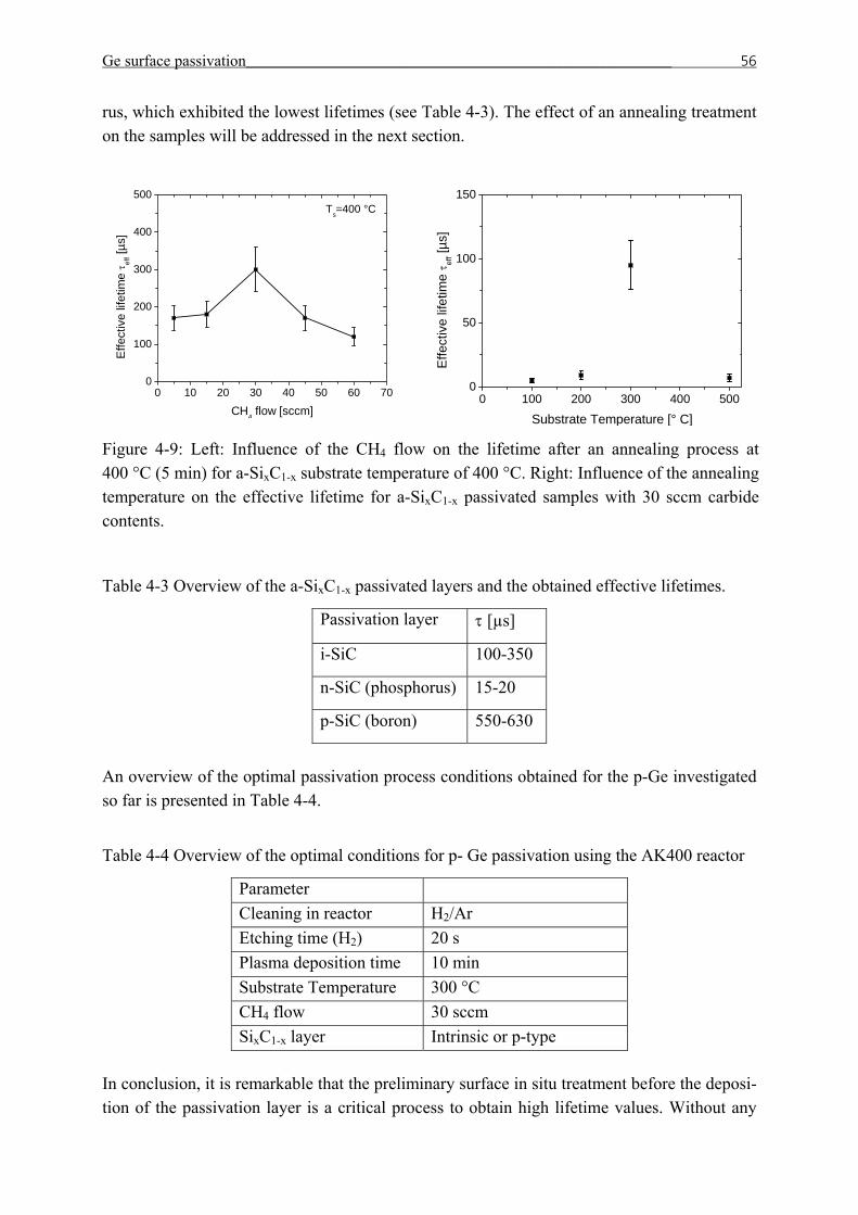
Ge surface passivation___________________________________________________________ 56
rus, which exhibited the lowest lifetimes (see Table 4-3). The effect of an annealing treatment on the samples will be addressed in the next section.
0 10 20 30 40 50 60 700
100
200
300
400
500
Effe
ctiv
e lif
etim
e τ ef
f [µs]
CH4 flow [sccm]
Ts=400 °C
0 100 200 300 400 500
0
50
100
150
Effe
ctiv
e lif
etim
e τ ef
f [µs
]
Substrate Temperature [° C]
Figure 4-9: Left: Influence of the CH4 flow on the lifetime after an annealing process at 400 °C (5 min) for a-SixC1-x substrate temperature of 400 °C. Right: Influence of the annealing temperature on the effective lifetime for a-SixC1-x passivated samples with 30 sccm carbide contents.
Table 4-3 Overview of the a-SixC1-x passivated layers and the obtained effective lifetimes.
Passivation layer τ [µs]
i-SiC 100-350
n-SiC (phosphorus) 15-20
p-SiC (boron) 550-630
An overview of the optimal passivation process conditions obtained for the p-Ge investigated so far is presented in Table 4-4.
Table 4-4 Overview of the optimal conditions for p- Ge passivation using the AK400 reactor
Parameter Cleaning in reactor H2/Ar Etching time (H2) 20 s Plasma deposition time 10 min Substrate Temperature 300 °C CH4 flow 30 sccm SixC1-x layer Intrinsic or p-type
In conclusion, it is remarkable that the preliminary surface in situ treatment before the deposi-tion of the passivation layer is a critical process to obtain high lifetime values. Without any
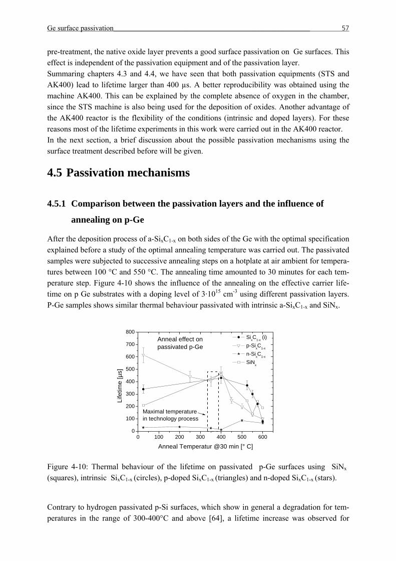
Ge surface passivation___________________________________________________________ 57
pre-treatment, the native oxide layer prevents a good surface passivation on Ge surfaces. This effect is independent of the passivation equipment and of the passivation layer. Summaring chapters 4.3 and 4.4, we have seen that both passivation equipments (STS and AK400) lead to lifetime larger than 400 µs. A better reproducibility was obtained using the machine AK400. This can be explained by the complete absence of oxygen in the chamber, since the STS machine is also being used for the deposition of oxides. Another advantage of the AK400 reactor is the flexibility of the conditions (intrinsic and doped layers). For these reasons most of the lifetime experiments in this work were carried out in the AK400 reactor. In the next section, a brief discussion about the possible passivation mechanisms using the surface treatment described before will be given.
4.5 Passivation mechanisms
4.5.1 Comparison between the passivation layers and the influence of
annealing on p-Ge
After the deposition process of a-SixC1-x on both sides of the Ge with the optimal specification explained before a study of the optimal annealing temperature was carried out. The passivated samples were subjected to successive annealing steps on a hotplate at air ambient for tempera-tures between 100 °C and 550 °C. The annealing time amounted to 30 minutes for each tem-perature step. Figure 4-10 shows the influence of the annealing on the effective carrier life-time on p Ge substrates with a doping level of 3·1015 cm-3 using different passivation layers. P-Ge samples shows similar thermal behaviour passivated with intrinsic a-SixC1-x and SiNx.
0 100 200 300 400 500 6000
100
200
300
400
500
600
700
800
SixC1-x (i) p-SixC1-x n-SixC1-x SiNx
Life
time
[µs]
Anneal Temperatur @30 min [° C]
Maximal temperature in technology process
Anneal effect onpassivated p-Ge
Figure 4-10: Thermal behaviour of the lifetime on passivated p-Ge surfaces using SiNx
(squares), intrinsic SixC1-x (circles), p-doped SixC1-x (triangles) and n-doped SixC1-x (stars).
Contrary to hydrogen passivated p-Si surfaces, which show in general a degradation for tem-peratures in the range of 300-400°C and above [64], a lifetime increase was observed for
Ge surface passivation___________________________________________________________ 58
i SixC1-x (circles) and SiNx (squares) passivation layers on p-Ge surfaces after annealing at 350-400 °C . For temperatures higher than 400 °C a decrease of the lifetime was observed probably due to degradation of the passivation layer. As described in [64], there exists a direct correlation between the lifetime degradation of the samples and the decrease of the Si-H bond density in the case of Si substrates annealed at 300-400 °C. There it was shown that the de-creasing hydrogen content in the a-SixC1-x matrix has no direct impact on the surface passiva-tion quality of Ge surfaces. This suggests that there are two different passivation mechanisms. On the one hand, the passivation of Si substrates and, on the other hand, the passivation of Ge substrates. In the case of SiNx, the model of chargeable defects (K centers) explains the high lifetime at 400 °C [33]. This leads to the presumption that a similar charge effect at the Ge/ a-SixC1-x interface may exist, originating from Si dangling bonds back bonded to one or more carbide atoms. In this case, the passivation mechanism would be addressed to a field effect at the interface. This assumption still has to be verified by other techniques, such as surface photo voltage (SPV) measurements.
A different behaviour was observed for p-doped and n-doped a-SixC1-x. The highest lifetime value (600 µs) was obtained with a lowly doped (B2H6=10 sccm) p-SixC1-x film. In contrast, when the passivation layer was doped with phosphorous, a very low lifetime was obtained. This behaviour may be explained considering a simplified band diagram using the computer program AFORS-HET [65]. The band diagrams for a-SixC1-x/p-Ge/a-SixC1-x struc-tures in the dark were simulated and are shown in Figure 4-11 and Figure 4-12. In this simplified model, electrons (minority carriers in p-Ge) at the Ge-surface are repelled due to the band-bending at the Ge/SiCx interface. This effect is more pronounced for p-doped amorphous silicon carbide (Figure 4-11 right). This leads to a reduction of the minority carri-ers at the interface which reduces the surface recombination velocity.
Figure 4-11: Band diagrams for a-SixC1-x p-Ge/ a-SixC1-x structures in the dark (assumption: no interface defects!). Left intrinsic a-SixC1-x and right p-doped a-SixC1-x [47].
On the other hand, the inverse band-bending indicated in Figure 4-12 in the case of n-doped a-SixC1-x results in an accumulation of minority carriers at the interface which leads to an en-hancement of the surface recombination [47]. Please keep in mind that these simplified band-
Ge surface passivation___________________________________________________________ 59
diagrams do not consider the certainly present interface defects. However, they give an idea of the influence of doped SixC1-x layers on the passivation quality of Ge surfaces. A significant decrease in the lifetime after a thermal treatment using p-doped a-SixC1-x pas-sivation layers was observed. This effect is at present not well understood. Further experi-ments have to be performed in order to clarify this behaviour.
Figure 4-12: Band diagrams for an n-doped a-SixC1-x /p-Ge/ a-SixC1-x structure in the dark (assumption: no interface defects) [47].
4.5.2 Comparison between the passivation layers and the influence of
annealing on i-Ge
In order to deepen the understanding of the involved passivation mechanisms and to find out more about the influence of the Ge specification, i-type Ge samples were passivated under identical conditions as presented before. Additionally, lattice matched n-GaInP passivation layers were also deposited onto Ge surfaces. The front surfaces of TPV cells described in chapter 5 were passivated with GaInP. The effectiveness of this passivation was evaluated with lifetime measurements as will be explained as follows.
Very lowly n-doped (2·1013 cm-3) Ge which can be considered as intrinsic Ge (ni=2·1013 cm-3), were supplied by Umicore with a thickness of 500 µm. Both sides were etched and polished by the manufacturer. SixC1-x passivation layers were deposited on Ge surfaces using optimal conditions described before (Table 4-4). A GaInP lattice matched layer was grown on both sides of the wafers using a MOVPE reactor. Native oxidation of Ge was removed using arsine at a temperature of 600 °C.
As Table 4-5 shows a high lifetime of 2450 µs was obtained for samples passivated by GaInP grown in a MOVPE. Crystallographic quality of the surface is more controlled compared to the passivation layer deposited using PECVD due to the deposition conditions. Therefore it is possible to assume a clean surface, which would lead to a lower density of defects at the Ge surface. Under this condition, no hydrogen is supposed to be incorporated in the layers and, therefore, dangling bonds saturated with H-atoms are unlikely. This is confirmed by the fact
Ge surface passivation___________________________________________________________ 60
that after annealing no (hydrogen) blisters occur in the case of GaInP passivated surfaces whereas blisters are frequently visible with a naked eye in the case of annealed hydrogenated amorphous passivation layers (a-SixC1-x, a-Si, SiNx). Due to the band gap of GaInP (1.67 eV) a remarkable field effect is also expected. Moreover, a high lifetime was achieved using p-doped or intrinsic a-SixC1-x. As in experiments with p-Ge, a low lifetime was obtained for samples passivated with phosphor doped a-SixC1-x. The poor passivation quality of n-SiCx both on p- and i-type Ge substrates indicates that the dominant mechanism in this case is probably rather defect recombination than linked to a field effect.
Table 4-5 Overview of the different passivation layers for i-type Ge (2·1013 cm-3) surfaces and the effective lifetime achieved in this work
Passivation layer τ [µs]
a-SixC1-x 1600±320
p- a-SixC1-x (bor) 1500±300
n- a-SixC1-x (Phosphor) 80±16
GaInP 2100-2450±400
The thermal behaviour of the effective lifetime in samples passivated with amorphous silicon carbide and GaInP is shown in Figure 4-13. The superior thermal stability using GaInP could be explained by the dominated field effect linked to the increased energy band gap of GaInP (1.67 eV) and the expected lower density of defects in an epitaxial layer. However more in-formation is necessary to explain this behaviour with scientific rigour.
0 100 200 300 400 500 6000
500
1000
1500
2000
2500
Life
time
[µs]
Anneal Temperatur @30 min [° C]
i-SixC1-x
n-SixC1-x
p-SixC1-x
GaInP
i-Ge
Figure 4-13: Comparison of thermal behaviour between intrinsic a-SixC1-x (open squares) p-doped a-SixC1-x (full squares), n-doped a-SixC1-x (triangles) and GaInP (stars) passivation.
Ge surface passivation___________________________________________________________ 61
In n a-SixC1-x as pointed out above, the defect recombination seems to be the dominant mechanism here and has to be particularly considered. The significant increase of the lifetime in this case for n-SiCx at a temperature of 400 °C might be due to phosphorus diffusion into the Ge surface, however this assumption still has to be verified by further analyses.
Conclusions: Ge passivation
- For p-Ge intrinsic and boron doped a-SixC1-x, a-Si and SiNx provide excellent surface passivation. a-SixC1-x and SiNx show a slight improvement after an annealing process at 400 °C. p-SixC1-x presents the best passivation quality in the as-deposited state with a lifetime higher than 600 µs, however, after the annealing treatment, a decrease of 40 % in the lifetime is observed at temperatures of 400 °C.
- For i-Ge, lattice matched GaInP grown in a MOVPE reactor provides the best surface passivation with a lifetime of 2450 µs with excellent temperature stability. Intrinsic and boron doped amorphous silicon carbide layers were also successful in providing a good passivation leading to lifetime values of 1000-1500 µs. In contrast, samples pas-sivated by n-SiCx show a very low passivation effect on i–Ge surfaces.
Using the optimized passivation process developed in this work, the bulk lifetime as a func-tion of the doping level in Ge will be determined and a discussion about the intrinsic recom-bination limits in Ge will be presented. The results proved to be very useful for the simula-tions which are carried out in the next chapters. Finally, a brief discussion about the diffusion length in the samples will motivate the use of this passivation technology for TPV cells and triple-junction cells described in chapters 5 and 6, respectively.
4.6 Characterization of passivation layers
4.6.1 Effective lifetime and separation of bulk lifetime
The quality of intrinsic a-SixC1-x passivation layers with the optimal specifications shown in Table 4-4 was characterised using the MW-PCD technique described in Chapter 3. The sur-face recombination velocity S was extracted independently of the bulk lifetime using the well-known expressions presented in Chapter 2 (Eq 2-43 and Eq 2-44 )
The validation of Eq 2-44 requires sufficiently low S-values and implies that the surface re-combination velocity is identical on both sides of the sample. Experimentally the separation of bulk and surface recombination is realized by lifetime measurements performed on a set of well passivated samples with the same material and surface properties, but varying thick-nesses W of the bulk material. For instance in the case of a p-type Ge wafer with a thickness of 500 µm and a doping level of 3·1015 cm-3, the value of 2Dn/W is equal to 4·103 cm/s, which presents an upper limit to the measurable S. The value of Dn was calculated using a mobility value taken from the literature [31]. The various thicknesses of the wafers were obtained by wet-chemical etching of the Ge substrate using H3PO4 with different etching times.
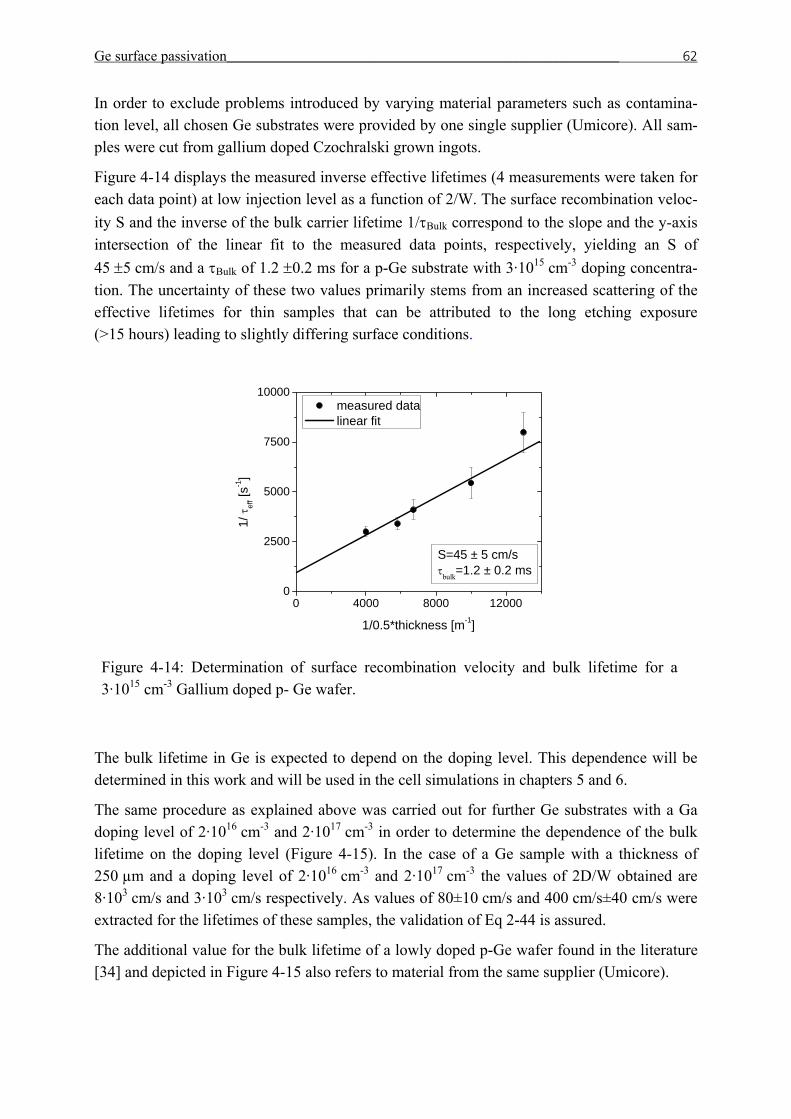
Ge surface passivation___________________________________________________________ 62
In order to exclude problems introduced by varying material parameters such as contamina-tion level, all chosen Ge substrates were provided by one single supplier (Umicore). All sam-ples were cut from gallium doped Czochralski grown ingots.
Figure 4-14 displays the measured inverse effective lifetimes (4 measurements were taken for each data point) at low injection level as a function of 2/W. The surface recombination veloc-ity S and the inverse of the bulk carrier lifetime 1/τBulk correspond to the slope and the y-axis intersection of the linear fit to the measured data points, respectively, yielding an S of 45 ±5 cm/s and a τBulk of 1.2 ±0.2 ms for a p-Ge substrate with 3·1015 cm-3 doping concentra-tion. The uncertainty of these two values primarily stems from an increased scattering of the effective lifetimes for thin samples that can be attributed to the long etching exposure (>15 hours) leading to slightly differing surface conditions.
0 4000 8000 120000
2500
5000
7500
10000
S=45 ± 5 cm/sτbulk=1.2 ± 0.2 ms
measured data linear fit
1/ τ
eff [
s-1]
1/0.5*thickness [m-1]
Figure 4-14: Determination of surface recombination velocity and bulk lifetime for a 3·1015 cm-3 Gallium doped p- Ge wafer.
The bulk lifetime in Ge is expected to depend on the doping level. This dependence will be determined in this work and will be used in the cell simulations in chapters 5 and 6.
The same procedure as explained above was carried out for further Ge substrates with a Ga doping level of 2·1016 cm-3 and 2·1017 cm-3 in order to determine the dependence of the bulk lifetime on the doping level (Figure 4-15). In the case of a Ge sample with a thickness of 250 µm and a doping level of 2·1016 cm-3 and 2·1017 cm-3 the values of 2D/W obtained are 8·103 cm/s and 3·103 cm/s respectively. As values of 80±10 cm/s and 400 cm/s±40 cm/s were extracted for the lifetimes of these samples, the validation of Eq 2-44 is assured.
The additional value for the bulk lifetime of a lowly doped p-Ge wafer found in the literature [34] and depicted in Figure 4-15 also refers to material from the same supplier (Umicore).
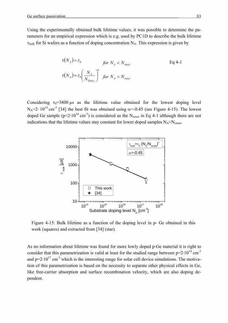
Ge surface passivation___________________________________________________________ 63
Using the experimentally obtained bulk lifetime values, it was possible to determine the pa-rameters for an empirical expression which is e.g. used by PC1D to describe the bulk lifetime τbulk for Si wafers as a function of doping concentration NA. This expression is given by
( )
( )α
ττ
ττ
⎟⎟⎠
⎞⎜⎜⎝
⎛=
=
Onset
AA
A
NNN
N
0
0
onsetA
onsetA
NNfor
NNfor
>
<
Eq 4-1
Considering τ0=3800 µs as the lifetime value obtained for the lowest doping level NA=2· 1014 cm-3 [34] the best fit was obtained using α=-0.45 (see Figure 4-15). The lowest doped Ge sample (p=2·1014 cm-3) is considered as the Nonset in Eq 4-1 although there are not indications that the lifetime values stay constant for lower doped samples NA<Nonset.
1014 1015 1016 1017 101810
100
1000
10000
This work [34]
α=-0.45
τ bu
lk [µ
s]
Substrate doping level NA [cm-3]
τbulk=τ0 (NA/Nonset)α
Figure 4-15: Bulk lifetime as a function of the doping level in p- Ge obtained in this work (squares) and extracted from [34] (star).
As no information about lifetime was found for more lowly doped p-Ge material it is right to consider that this parametrization is valid at least for the studied range between p=2·1014 cm-3 and p=2·1017 cm-3 which is the interesting range for solar cell device simulations. The motiva-tion of this parametrization is based on the necessity to separate other physical effects in Ge, like free-carrier absorption and surface recombination velocity, which are also doping de-pendent.
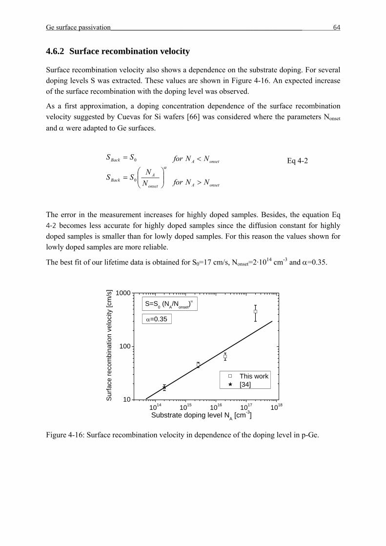
Ge surface passivation___________________________________________________________ 64
4.6.2 Surface recombination velocity
Surface recombination velocity also shows a dependence on the substrate doping. For several doping levels S was extracted. These values are shown in Figure 4-16. An expected increase of the surface recombination with the doping level was observed.
As a first approximation, a doping concentration dependence of the surface recombination velocity suggested by Cuevas for Si wafers [66] was considered where the parameters Nonset and α were adapted to Ge surfaces.
α
⎟⎟⎠
⎞⎜⎜⎝
⎛=
=
onset
ABack
Back
NN
SS
SS
0
0
onsetA
onsetA
NNfor
NNfor
>
<
Eq 4-2
The error in the measurement increases for highly doped samples. Besides, the equation Eq
4-2 becomes less accurate for highly doped samples since the diffusion constant for highly doped samples is smaller than for lowly doped samples. For this reason the values shown for lowly doped samples are more reliable.
The best fit of our lifetime data is obtained for S0=17 cm/s, Nonset=2·1014 cm-3 and α=0.35.
1014 1015 1016 1017 101810
100
1000
This work [34]
Sur
face
reco
mbi
natio
n ve
loci
ty [c
m/s
]
Substrate doping level NA [cm-3]
S=S0 (NA/Nonset)α
α=0.35
Figure 4-16: Surface recombination velocity in dependence of the doping level in p-Ge.
Ge surface passivation___________________________________________________________ 65
4.7 Impact of intrinsic limits
The very low surface recombination velocities achieved allow for further insight into the in-trinsic recombination mechanisms in Ge. Coefficients of radiative and Auger recombination were determined in this work by means of effective lifetime measurements at high injection levels. However, as discussed in chapter 3, these results have to be considered cautiously as the MW-PCD technique becomes increasingly erroneous for Ge samples when aiming at high excess carrier densities.
Effective lifetimes in samples with a-SixC1-x passivation layers were measured in the range of 1013 cm-3<Δn<1017 cm-3). The substrates used in this study were p-type Ge wafer (500 µm thickness) with a doping level of (1.2±0.2)·1014 cm-3 (ρ= 20-25 Ωcm), etched and polished on both sides. With this surface treatment, an effective lifetime between 550 µs and 1 ms was obtained at a low injection level. A low surface recombination is a prerequisite for the achievement of high injection levels during light exposure. Under these conditions the intrin-sic recombination mechanisms such as Auger and radiative dominate the lifetime behaviour and surface and SRH bulk recombination can be neglected. Thus, lifetime measurements at high injection levels give the opportunity to identify and determine the impact of the intrinsic lifetime limits on Ge substrates.
The measurement of the effective minority carrier lifetime was performed by the microwave-detected photoconductance decay (MW-PCD) technique. As it was discussed in chapter 3 the lifetime value determined by the MW-PCD method is the differential effective lifetime τeff,diff. For lifetime measurements with Δn < 5·1015 cm-3, where hardly any injection dependence of the lifetime was found, the assumption τlow,eff,diff = τlow,eff,abs= τeff, where τlow,eff,abs is the abso-lute effective lifetime, provides a good approximation. However, this relation does not hold in the high injection regime any more due to the pronounced injection dependence of the recom-bination dynamics (lifetimes shown in Figure 4-17). In this case, the absolute effective life-time τeff,abs was calculated using an iterative method proposed by Aberle [33] and generalised by S.Rein [49] as it was discussed in section 3.2.3.
Using this method, the absolute effective carrier lifetime as a function of the injection level has been calculated for three samples with a doping level of (1.2±0.2) 1014 cm-3 and different SixC1-x layers (Figure 4-17).
In the high injection region (Δn>1016 cm-3), the effective lifetime is dominated by radiative and Auger recombination. As discussed in chapter 2, the basic expression for the effective lifetime in the case of high level injection (HLI) is given by Eq 4-3 and Eq 4-4, where A cor-responds to the Shockley-Read-Hall (SRH) channel. This term is considered approximately equal to the inverse of the lifetime measured at low injection level. It is assumed constant with the injection level. Ca and B represent the so-called ambipolar Auger coefficient and the ra-diative coefficient, respectively.
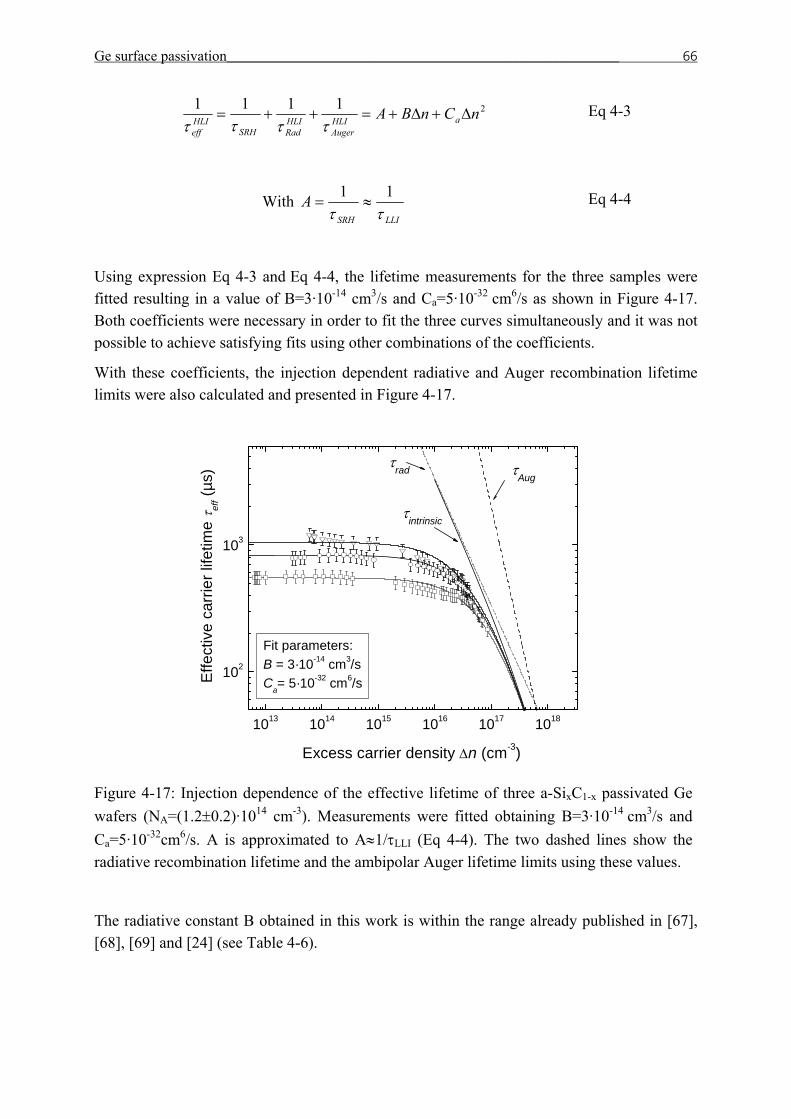
Ge surface passivation___________________________________________________________ 66
21111 nCnBA aHLIAuger
HLIRadSRH
HLIeff
Δ+Δ+=++=ττττ
Eq 4-3
With LLISRH
Aττ
11≈= Eq 4-4
Using expression Eq 4-3 and Eq 4-4, the lifetime measurements for the three samples were fitted resulting in a value of B=3·10-14 cm3/s and Ca=5·10-32 cm6/s as shown in Figure 4-17. Both coefficients were necessary in order to fit the three curves simultaneously and it was not possible to achieve satisfying fits using other combinations of the coefficients.
With these coefficients, the injection dependent radiative and Auger recombination lifetime limits were also calculated and presented in Figure 4-17.
1013 1014 1015 1016 1017 1018
102
103
τintrinsic
Fit parameters: B = 3·10-14 cm3/sCa= 5·10-32 cm6/s
τAug τrad
Effe
ctiv
e ca
rrie
r life
time
τ eff (µ
s)
Excess carrier density Δn (cm-3)
Figure 4-17: Injection dependence of the effective lifetime of three a-SixC1-x passivated Ge wafers (NA=(1.2±0.2)·1014 cm-3). Measurements were fitted obtaining B=3·10-14 cm3/s and Ca=5·10-32cm6/s. A is approximated to A≈1/τLLI (Eq 4-4). The two dashed lines show the radiative recombination lifetime and the ambipolar Auger lifetime limits using these values.
The radiative constant B obtained in this work is within the range already published in [67], [68], [69] and [24] (see Table 4-6).
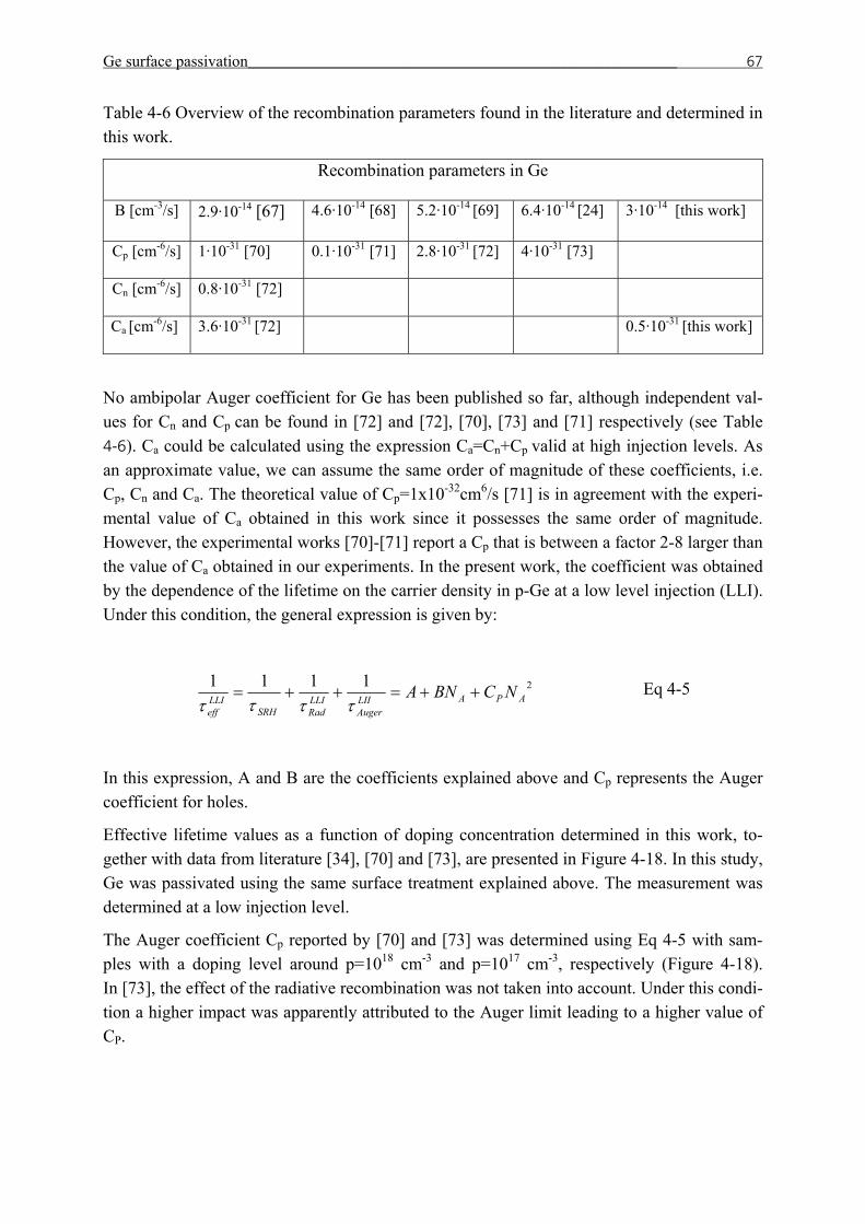
Ge surface passivation___________________________________________________________ 67
Table 4-6 Overview of the recombination parameters found in the literature and determined in this work.
Recombination parameters in Ge
B [cm-3/s] 2.9·10-14 [67] 4.6·10-14 [68] 5.2·10-14 [69] 6.4·10-14 [24] 3·10-14 [this work]
Cp [cm-6/s] 1·10-31 [70] 0.1·10-31 [71] 2.8·10-31 [72] 4·10-31 [73]
Cn [cm-6/s] 0.8·10-31 [72]
Ca [cm-6/s] 3.6·10-31 [72] 0.5·10-31 [this work]
No ambipolar Auger coefficient for Ge has been published so far, although independent val-ues for Cn and Cp can be found in [72] and [72], [70], [73] and [71] respectively (see Table
4-6). Ca could be calculated using the expression Ca=Cn+Cp valid at high injection levels. As an approximate value, we can assume the same order of magnitude of these coefficients, i.e. Cp, Cn and Ca. The theoretical value of Cp=1x10-32cm6/s [71] is in agreement with the experi-mental value of Ca obtained in this work since it possesses the same order of magnitude. However, the experimental works [70]-[71] report a Cp that is between a factor 2-8 larger than the value of Ca obtained in our experiments. In the present work, the coefficient was obtained by the dependence of the lifetime on the carrier density in p-Ge at a low level injection (LLI). Under this condition, the general expression is given by:
21111APALII
AugerLLIRadSRH
LLIeff
NCBNA ++=++=ττττ
Eq 4-5
In this expression, A and B are the coefficients explained above and Cp represents the Auger coefficient for holes.
Effective lifetime values as a function of doping concentration determined in this work, to-gether with data from literature [34], [70] and [73], are presented in Figure 4-18. In this study, Ge was passivated using the same surface treatment explained above. The measurement was determined at a low injection level.
The Auger coefficient Cp reported by [70] and [73] was determined using Eq 4-5 with sam-ples with a doping level around p=1018 cm-3 and p=1017 cm-3, respectively (Figure 4-18). In [73], the effect of the radiative recombination was not taken into account. Under this condi-tion a higher impact was apparently attributed to the Auger limit leading to a higher value of CP.
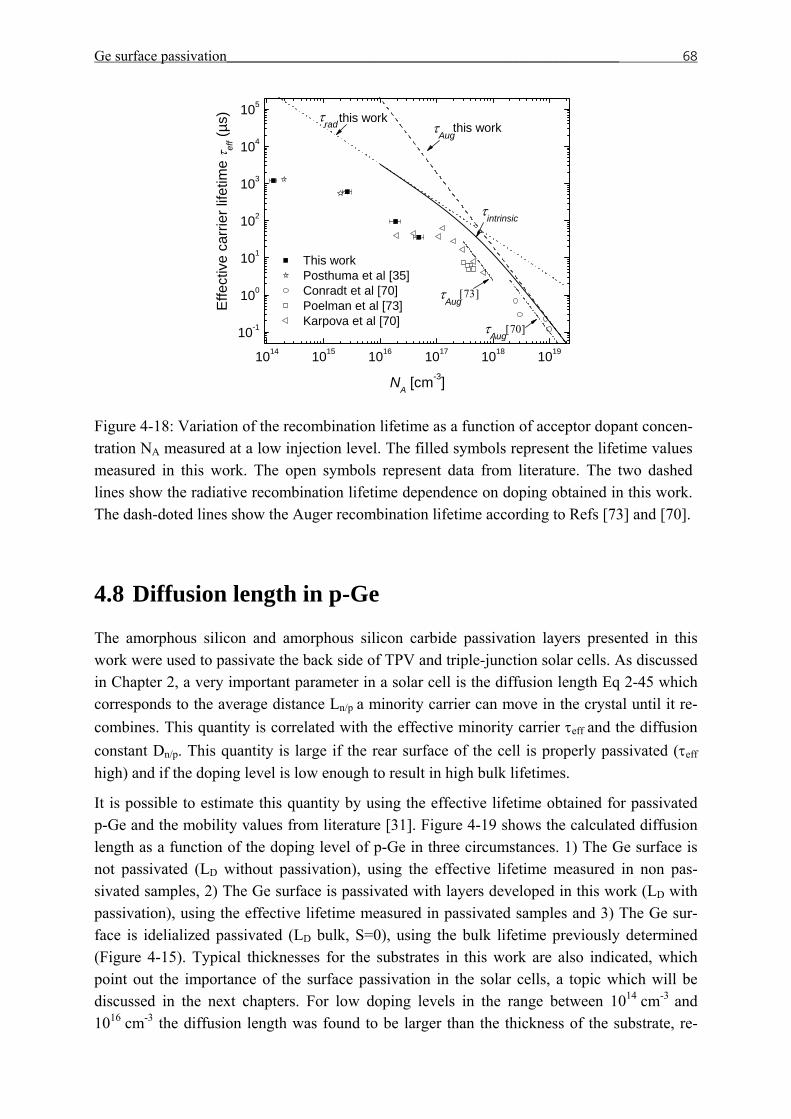
Ge surface passivation___________________________________________________________ 68
1014 1015 1016 1017 1018 1019
10-1
100
101
102
103
104
105
[73]
[70]
this workthis work
τintrinsic
τAug
τrad
τAug
Effe
ctiv
e ca
rrie
r life
time
τ eff (µ
s)
NA [cm-3]
This work Posthuma et al [35] Conradt et al [70] Poelman et al [73] Karpova et al [70]
τAug
Figure 4-18: Variation of the recombination lifetime as a function of acceptor dopant concen-tration NA measured at a low injection level. The filled symbols represent the lifetime values measured in this work. The open symbols represent data from literature. The two dashed lines show the radiative recombination lifetime dependence on doping obtained in this work. The dash-doted lines show the Auger recombination lifetime according to Refs [73] and [70].
4.8 Diffusion length in p-Ge
The amorphous silicon and amorphous silicon carbide passivation layers presented in this work were used to passivate the back side of TPV and triple-junction solar cells. As discussed in Chapter 2, a very important parameter in a solar cell is the diffusion length Eq 2-45 which corresponds to the average distance Ln/p a minority carrier can move in the crystal until it re-combines. This quantity is correlated with the effective minority carrier τeff and the diffusion constant Dn/p. This quantity is large if the rear surface of the cell is properly passivated (τeff high) and if the doping level is low enough to result in high bulk lifetimes.
It is possible to estimate this quantity by using the effective lifetime obtained for passivated p-Ge and the mobility values from literature [31]. Figure 4-19 shows the calculated diffusion length as a function of the doping level of p-Ge in three circumstances. 1) The Ge surface is not passivated (LD without passivation), using the effective lifetime measured in non pas-sivated samples, 2) The Ge surface is passivated with layers developed in this work (LD with passivation), using the effective lifetime measured in passivated samples and 3) The Ge sur-face is idelialized passivated (LD bulk, S=0), using the bulk lifetime previously determined (Figure 4-15). Typical thicknesses for the substrates in this work are also indicated, which point out the importance of the surface passivation in the solar cells, a topic which will be discussed in the next chapters. For low doping levels in the range between 1014 cm-3 and 1016 cm-3 the diffusion length was found to be larger than the thickness of the substrate, re-
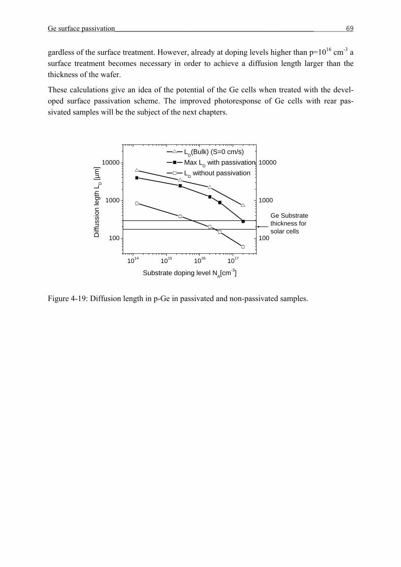
Ge surface passivation___________________________________________________________ 69
gardless of the surface treatment. However, already at doping levels higher than p=1016 cm-3 a surface treatment becomes necessary in order to achieve a diffusion length larger than the thickness of the wafer.
These calculations give an idea of the potential of the Ge cells when treated with the devel-oped surface passivation scheme. The improved photoresponse of Ge cells with rear pas-sivated samples will be the subject of the next chapters.
1014 1015 1016 1017
100
1000
10000
100
1000
10000 LD(Bulk) (S=0 cm/s) Max LD with passivation LD without passivation
Diff
ussi
on le
gth
L D [µ
m]
Substrate doping level NA[cm-3]
Ge Substrate thickness forsolar cells
Figure 4-19: Diffusion length in p-Ge in passivated and non-passivated samples.

Ge surface passivation___________________________________________________________ 70
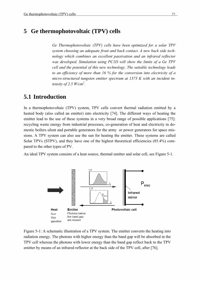
Ge thermophotovoltaic (TPV) cells 71
5 Ge thermophotovoltaic (TPV) cells
Ge Thermophotovoltaic (TPV) cells have been optimized for a solar TPV system choosing an adequate front and back contact. A new back side tech-nology which combines an excellent passivation and an infrared reflector was developed. Simulation using PC1D will show the limits of a Ge TPV cell and the potential of this new technology. The suitable technology leads to an efficiency of more than 16 % for the conversion into electricity of a micro-structured tungsten emitter spectrum at 1373 K with an incident in-tensity of 2.5 W/cm2.
5.1 Introduction
In a thermophotovoltaic (TPV) system, TPV cells convert thermal radiation emitted by a heated body (also called an emitter) into electricity [74]. The different ways of heating the emitter lead to the use of these systems in a very broad range of possible applications [75]: recycling waste energy from industrial processes, co-generation of heat and electricity in do-mestic boilers silent and portable generators for the army or power generators for space mis-sions. A TPV system can also use the sun for heating the emitter. These systems are called Solar TPVs (STPV), and they have one of the highest theoretical efficiencies (85.4%) com-pared to the other types of PV.
An ideal TPV system consists of a heat source, thermal emitter and solar cell, see Figure 5-1.
Figure 5-1: A schematic illustration of a TPV system. The emitter converts the heating into radiation energy. The photons with higher energy than the band gap will be absorbed in the TPV cell whereas the photons with lower energy than the band gap reflect back to the TPV emitter by means of an infrared reflector at the back side of the TPV cell, after [76].
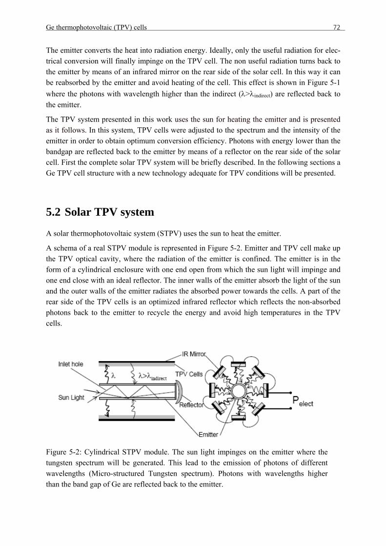
Ge thermophotovoltaic (TPV) cells 72
The emitter converts the heat into radiation energy. Ideally, only the useful radiation for elec-trical conversion will finally impinge on the TPV cell. The non useful radiation turns back to the emitter by means of an infrared mirror on the rear side of the solar cell. In this way it can be reabsorbed by the emitter and avoid heating of the cell. This effect is shown in Figure 5-1 where the photons with wavelength higher than the indirect (λ>λindirect) are reflected back to the emitter.
The TPV system presented in this work uses the sun for heating the emitter and is presented as it follows. In this system, TPV cells were adjusted to the spectrum and the intensity of the emitter in order to obtain optimum conversion efficiency. Photons with energy lower than the bandgap are reflected back to the emitter by means of a reflector on the rear side of the solar cell. First the complete solar TPV system will be briefly described. In the following sections a Ge TPV cell structure with a new technology adequate for TPV conditions will be presented.
5.2 Solar TPV system
A solar thermophotovoltaic system (STPV) uses the sun to heat the emitter.
A schema of a real STPV module is represented in Figure 5-2. Emitter and TPV cell make up the TPV optical cavity, where the radiation of the emitter is confined. The emitter is in the form of a cylindrical enclosure with one end open from which the sun light will impinge and one end close with an ideal reflector. The inner walls of the emitter absorb the light of the sun and the outer walls of the emitter radiates the absorbed power towards the cells. A part of the rear side of the TPV cells is an optimized infrared reflector which reflects the non-absorbed photons back to the emitter to recycle the energy and avoid high temperatures in the TPV cells.
Figure 5-2: Cylindrical STPV module. The sun light impinges on the emitter where the tungsten spectrum will be generated. This lead to the emission of photons of different wavelengths (Micro-structured Tungsten spectrum). Photons with wavelengths higher than the band gap of Ge are reflected back to the emitter.
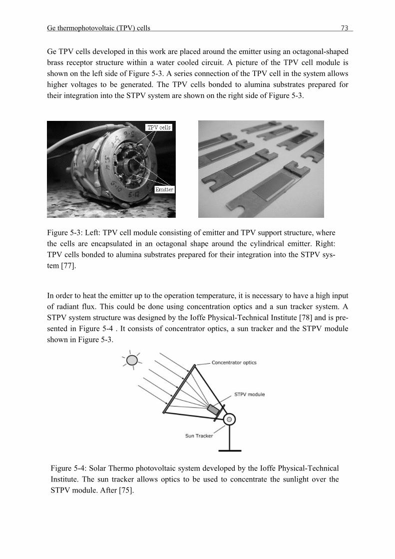
Ge thermophotovoltaic (TPV) cells 73
Ge TPV cells developed in this work are placed around the emitter using an octagonal-shaped brass receptor structure within a water cooled circuit. A picture of the TPV cell module is shown on the left side of Figure 5-3. A series connection of the TPV cell in the system allows higher voltages to be generated. The TPV cells bonded to alumina substrates prepared for their integration into the STPV system are shown on the right side of Figure 5-3.
Figure 5-3: Left: TPV cell module consisting of emitter and TPV support structure, where the cells are encapsulated in an octagonal shape around the cylindrical emitter. Right: TPV cells bonded to alumina substrates prepared for their integration into the STPV sys-tem [77].
In order to heat the emitter up to the operation temperature, it is necessary to have a high input of radiant flux. This could be done using concentration optics and a sun tracker system. A STPV system structure was designed by the Ioffe Physical-Technical Institute [78] and is pre-sented in Figure 5-4 . It consists of concentrator optics, a sun tracker and the STPV module shown in Figure 5-3.
Figure 5-4: Solar Thermo photovoltaic system developed by the Ioffe Physical-Technical Institute. The sun tracker allows optics to be used to concentrate the sunlight over the STPV module. After [75].
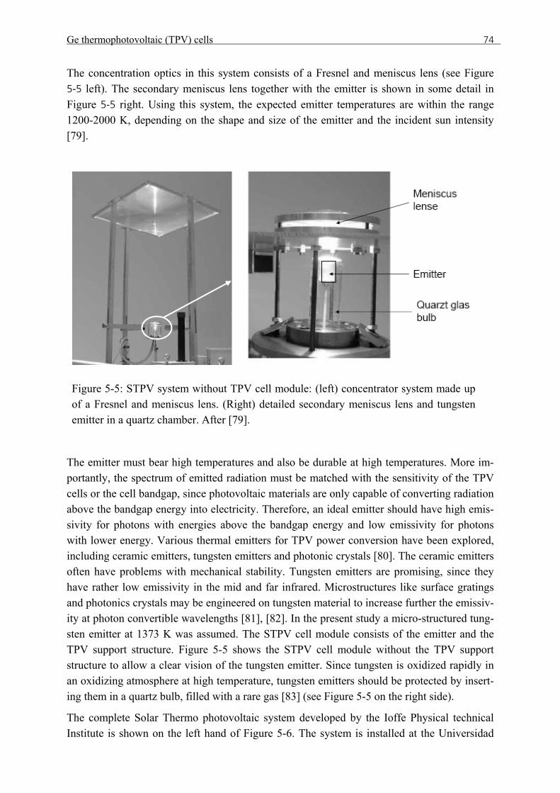
Ge thermophotovoltaic (TPV) cells 74
The concentration optics in this system consists of a Fresnel and meniscus lens (see XFigure
5-5 left). The secondary meniscus lens together with the emitter is shown in some detail in XFigure 5-5 right. Using this system, the expected emitter temperatures are within the range 1200-2000 K, depending on the shape and size of the emitter and the incident sun intensity [79].
Figure 5-5: STPV system without TPV cell module: (left) concentrator system made up of a Fresnel and meniscus lens. (Right) detailed secondary meniscus lens and tungsten emitter in a quartz chamber. After [79].
The emitter must bear high temperatures and also be durable at high temperatures. More im-portantly, the spectrum of emitted radiation must be matched with the sensitivity of the TPV cells or the cell bandgap, since photovoltaic materials are only capable of converting radiation above the bandgap energy into electricity. Therefore, an ideal emitter should have high emis-sivity for photons with energies above the bandgap energy and low emissivity for photons with lower energy. Various thermal emitters for TPV power conversion have been explored, including ceramic emitters, tungsten emitters and photonic crystals [80]. The ceramic emitters often have problems with mechanical stability. Tungsten emitters are promising, since they have rather low emissivity in the mid and far infrared. Microstructures like surface gratings and photonics crystals may be engineered on tungsten material to increase further the emissiv-ity at photon convertible wavelengths [81], [82]. In the present study a micro-structured tung-sten emitter at 1373 K was assumed. The STPV cell module consists of the emitter and the TPV support structure. XFigure 5-5 shows the STPV cell module without the TPV support structure to allow a clear vision of the tungsten emitter. Since tungsten is oxidized rapidly in an oxidizing atmosphere at high temperature, tungsten emitters should be protected by insert-ing them in a quartz bulb, filled with a rare gas [83] (see XFigure 5-5 on the right side).
The complete Solar Thermo photovoltaic system developed by the Ioffe Physical technical Institute is shown on the left hand of Figure 5-6. The system is installed at the Universidad
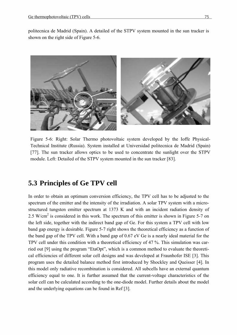
Ge thermophotovoltaic (TPV) cells 75
politecnica de Madrid (Spain). A detailed of the STPV system mounted in the sun tracker is shown on the right side of Figure 5-6.
Figure 5-6: Right: Solar Thermo photovoltaic system developed by the Ioffe Physical-Technical Institute (Russia). System installed at Universidad politecnica de Madrid (Spain) [77]. The sun tracker allows optics to be used to concentrate the sunlight over the STPV module. Left: Detailed of the STPV system mounted in the sun tracker [83].
5.3 Principles of Ge TPV cell
In order to obtain an optimum conversion efficiency, the TPV cell has to be adjusted to the spectrum of the emitter and the intensity of the irradiation. A solar TPV system with a micro-structured tungsten emitter spectrum at 1373 K and with an incident radiation density of 2.5 W/cm2 is considered in this work. The spectrum of this emitter is shown in XFigure 5-7X on the left side, together with the indirect band gap of Ge. For this system a TPV cell with low band gap energy is desirable. XFigure 5-7X right shows the theoretical efficiency as a function of the band gap of the TPV cell. With a band gap of 0.67 eV Ge is a nearly ideal material for the TPV cell under this condition with a theoretical efficiency of 47 %. This simulation was car-ried out [9] using the program “EtaOpt”, which is a common method to evaluate the theoreti-cal efficiencies of different solar cell designs and was developed at Fraunhofer ISE [3]. This program uses the detailed balance method first introduced by Shockley and Queisser [4]. In this model only radiative recombination is considered. All subcells have an external quantum efficiency equal to one. It is further assumed that the current-voltage characteristics of the solar cell can be calculated according to the one-diode model. Further details about the model and the underlying equations can be found in Ref [3].
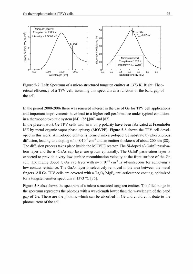
Ge thermophotovoltaic (TPV) cells 76
500 1000 1500 20000
1
2
3
4Microstructured
Tungsten at 1373 KIntensity = 2.5 W/cm2
Pow
er d
ensi
ty [W
/μm
cm
2 ]
Wavelength [nm]
Eg,ind
0.0 0.2 0.4 0.6 0.8 1.0 1.20
10
20
30
40
50
Microstructured Tungsten at 1373 K
Intensity = 2.5 W/cm2Theo
retic
al e
ffici
ency
[%]
Bandgap energy [eV]
GeEgap=0.67 eV
Figure 5-7: Left: Spectrum of a micro-structured tungsten emitter at 1373 K. Right: Theo-retical efficiency of a TPV cell, assuming this spectrum as a function of the band gap of the cell.
In the period 2000-2006 there was renewed interest in the use of Ge for TPV cell applications and important improvements have lead to a higher cell performance under typical conditions in a thermophotovoltaic system [84], [85],[86] and [87]. In the present work Ge TPV cells with an n-on-p polarity have been fabricated at Fraunhofer ISE by metal organic vapor phase epitaxy (MOVPE). Figure 5-8X shows the TPV cell devel-oped in this work. An n-doped emitter is formed into a p-doped Ge substrate by phosphorous diffusion, leading to a doping of n=8·1018 cm-3 and an emitter thickness of about 200 nm [88]. The diffusion process takes place inside the MOVPE reactor. The Si-doped n+-GaInP passiva-tion layer and the n+-GaAs cap layer are grown epitaxially. The GaInP passivation layer is expected to provide a very low surface recombination velocity at the front surface of the Ge cell. The highly doped GaAs cap layer with n= 5·1018 cm-3 is advantageous for achieving a low contact resistance. The GaAs layer is selectively removed in the area between the metal fingers. All Ge TPV cells are covered with a Ta2O5/MgF2 anti-reflectance coating, optimized for a tungsten emitter spectrum at 1373 °C [76].
XFigure 5-8X also shows the spectrum of a micro-structured tungsten emitter. The filled range in the spectrum represents the photons with a wavelength lower than the wavelength of the band gap of Ge. These are the photons which can be absorbed in Ge and could contribute to the photocurrent of the cell.
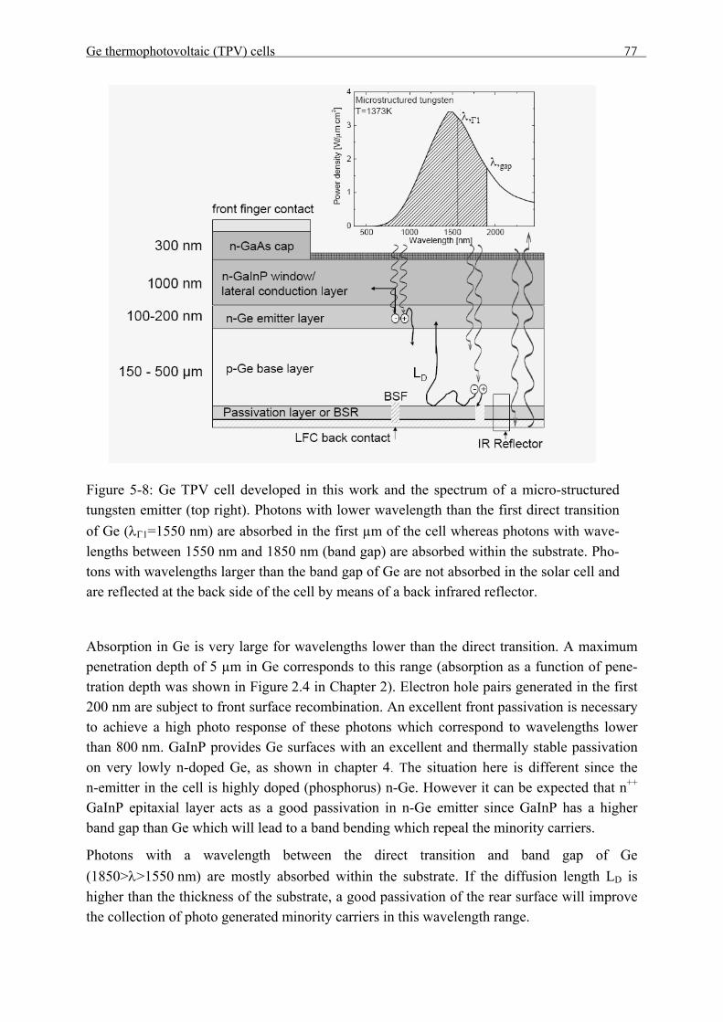
Ge thermophotovoltaic (TPV) cells 77
Figure 5-8: Ge TPV cell developed in this work and the spectrum of a micro-structured tungsten emitter (top right). Photons with lower wavelength than the first direct transition of Ge (λΓ1=1550 nm) are absorbed in the first µm of the cell whereas photons with wave-lengths between 1550 nm and 1850 nm (band gap) are absorbed within the substrate. Pho-tons with wavelengths larger than the band gap of Ge are not absorbed in the solar cell and are reflected at the back side of the cell by means of a back infrared reflector.
Absorption in Ge is very large for wavelengths lower than the direct transition. A maximum penetration depth of 5 µm in Ge corresponds to this range (absorption as a function of pene-tration depth was shown in Figure 2.4 in Chapter 2). Electron hole pairs generated in the first 200 nm are subject to front surface recombination. An excellent front passivation is necessary to achieve a high photo response of these photons which correspond to wavelengths lower than 800 nm. GaInP provides Ge surfaces with an excellent and thermally stable passivation on very lowly n-doped Ge, as shown in chapter 4. The situation here is different since the n-emitter in the cell is highly doped (phosphorus) n-Ge. However it can be expected that n++ GaInP epitaxial layer acts as a good passivation in n-Ge emitter since GaInP has a higher band gap than Ge which will lead to a band bending which repeal the minority carriers.
Photons with a wavelength between the direct transition and band gap of Ge (1850>λ>1550 nm) are mostly absorbed within the substrate. If the diffusion length LD is higher than the thickness of the substrate, a good passivation of the rear surface will improve the collection of photo generated minority carriers in this wavelength range.
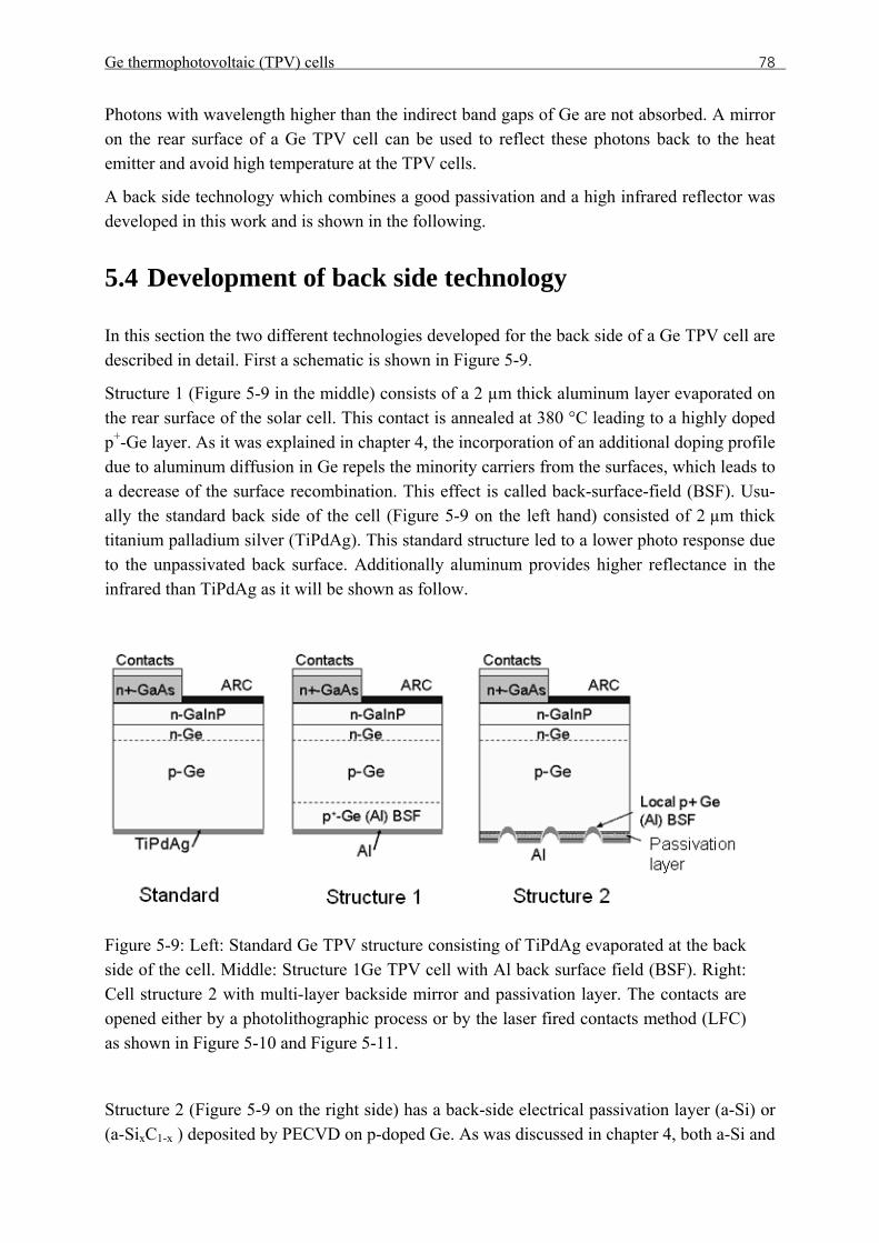
Ge thermophotovoltaic (TPV) cells 78
Photons with wavelength higher than the indirect band gaps of Ge are not absorbed. A mirror on the rear surface of a Ge TPV cell can be used to reflect these photons back to the heat emitter and avoid high temperature at the TPV cells.
A back side technology which combines a good passivation and a high infrared reflector was developed in this work and is shown in the following.
5.4 Development of back side technology
In this section the two different technologies developed for the back side of a Ge TPV cell are described in detail. First a schematic is shown in XFigure 5-9X.
Structure 1 (Figure 5-9 in the middle) consists of a 2 µm thick aluminum layer evaporated on the rear surface of the solar cell. This contact is annealed at 380 °C leading to a highly doped p+-Ge layer. As it was explained in chapter 4, the incorporation of an additional doping profile due to aluminum diffusion in Ge repels the minority carriers from the surfaces, which leads to a decrease of the surface recombination. This effect is called back-surface-field (BSF). Usu-ally the standard back side of the cell (Figure 5-9 on the left hand) consisted of 2 µm thick titanium palladium silver (TiPdAg). This standard structure led to a lower photo response due to the unpassivated back surface. Additionally aluminum provides higher reflectance in the infrared than TiPdAg as it will be shown as follow.
Figure 5-9: Left: Standard Ge TPV structure consisting of TiPdAg evaporated at the back side of the cell. Middle: Structure 1Ge TPV cell with Al back surface field (BSF). Right: Cell structure 2 with multi-layer backside mirror and passivation layer. The contacts are opened either by a photolithographic process or by the laser fired contacts method (LFC) as shown in XFigure 5-10 and Figure 5-11.
Structure 2 (Figure 5-9 on the right side) has a back-side electrical passivation layer (a-Si) or (a-SixC1-x ) deposited by PECVD on p-doped Ge. As was discussed in chapter 4, both a-Si and
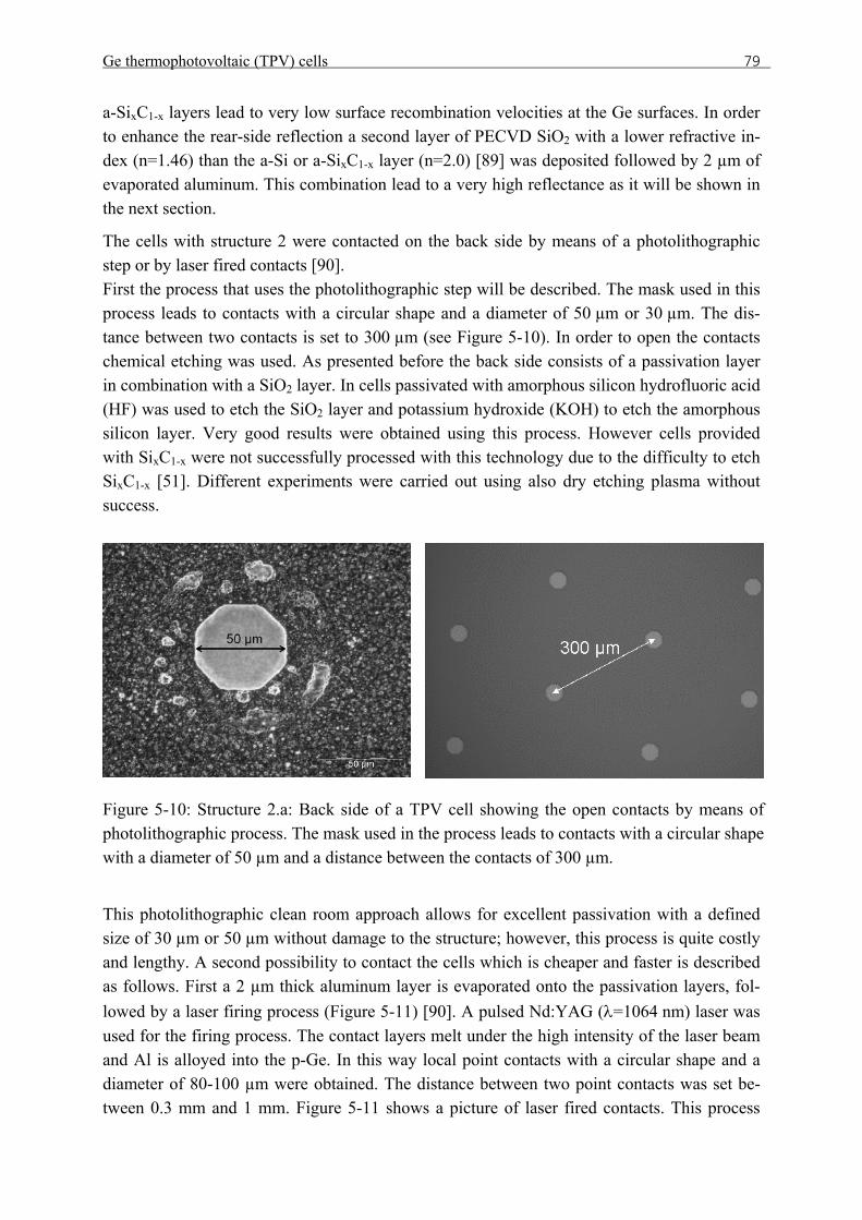
Ge thermophotovoltaic (TPV) cells 79
a-SixC1-x layers lead to very low surface recombination velocities at the Ge surfaces. In order to enhance the rear-side reflection a second layer of PECVD SiO2 with a lower refractive in-dex (n=1.46) than the a-Si or a-SixC1-x layer (n=2.0) [89] was deposited followed by 2 µm of evaporated aluminum. This combination lead to a very high reflectance as it will be shown in the next section.
The cells with structure 2 were contacted on the back side by means of a photolithographic step or by laser fired contacts [90]. First the process that uses the photolithographic step will be described. The mask used in this process leads to contacts with a circular shape and a diameter of 50 µm or 30 µm. The dis-tance between two contacts is set to 300 µm (see Figure 5-10). In order to open the contacts chemical etching was used. As presented before the back side consists of a passivation layer in combination with a SiO2 layer. In cells passivated with amorphous silicon hydrofluoric acid (HF) was used to etch the SiO2 layer and potassium hydroxide (KOH) to etch the amorphous silicon layer. Very good results were obtained using this process. However cells provided with SixC1-x were not successfully processed with this technology due to the difficulty to etch SixC1-x [51]. Different experiments were carried out using also dry etching plasma without success.
Figure 5-10: Structure 2.a: Back side of a TPV cell showing the open contacts by means of photolithographic process. The mask used in the process leads to contacts with a circular shape with a diameter of 50 µm and a distance between the contacts of 300 µm.
This photolithographic clean room approach allows for excellent passivation with a defined size of 30 µm or 50 µm without damage to the structure; however, this process is quite costly and lengthy. A second possibility to contact the cells which is cheaper and faster is described as follows. First a 2 µm thick aluminum layer is evaporated onto the passivation layers, fol-lowed by a laser firing process (Figure 5-11) [90]. A pulsed Nd:YAG (λ=1064 nm) laser was used for the firing process. The contact layers melt under the high intensity of the laser beam and Al is alloyed into the p-Ge. In this way local point contacts with a circular shape and a diameter of 80-100 µm were obtained. The distance between two point contacts was set be-tween 0.3 mm and 1 mm. Figure 5-11 shows a picture of laser fired contacts. This process
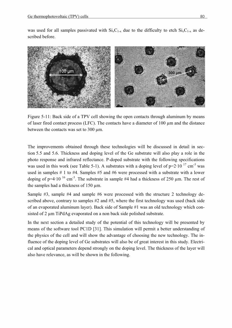
Ge thermophotovoltaic (TPV) cells 80
was used for all samples passivated with SixC1-x due to the difficulty to etch SixC1-x as de-scribed before.
Figure 5-11: Back side of a TPV cell showing the open contacts through aluminum by means of laser fired contact process (LFC). The contacts have a diameter of 100 µm and the distance between the contacts was set to 300 µm.
The improvements obtained through these technologies will be discussed in detail in sec-tion 5.5 and 5.6. Thickness and doping level of the Ge substrate will also play a role in the photo response and infrared reflectance. P-doped substrate with the following specifications was used in this work (see XTable 5-1X). A substrates with a doping level of p=2·10 17 cm-3 was used in samples # 1 to #4. Samples #5 and #6 were processed with a substrate with a lower doping of p=4·10 16 cm-3. The substrate in sample #4 had a thickness of 250 µm. The rest of the samples had a thickness of 150 µm.
Sample #3, sample #4 and sample #6 were processed with the structure 2 technology de-scribed above, contrary to samples #2 and #5, where the first technology was used (back side of an evaporated aluminum layer). Back side of Sample #1 was an old technology which con-sisted of 2 µm TiPdAg evaporated on a non back side polished substrate.
In the next section a detailed study of the potential of this technology will be presented by means of the software tool PC1D [31]. This simulation will permit a better understanding of the physics of the cell and will show the advantage of choosing the new technology. The in-fluence of the doping level of Ge substrates will also be of great interest in this study. Electri-cal and optical parameters depend strongly on the doping level. The thickness of the layer will also have relevance, as will be shown in the following.
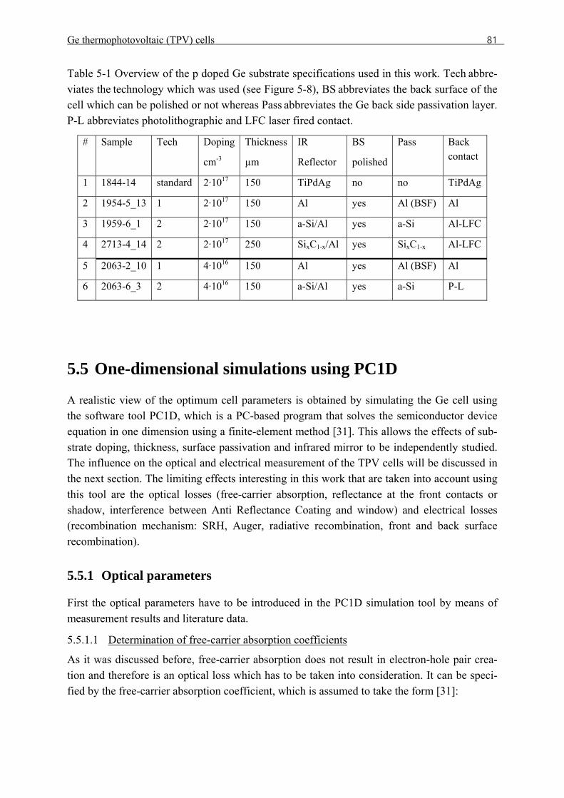
Ge thermophotovoltaic (TPV) cells 81
Table 5-1 Overview of the p doped Ge substrate specifications used in this work. Tech abbre-viates the technology which was used (see Figure 5-8), BS abbreviates the back surface of the cell which can be polished or not whereas Pass abbreviates the Ge back side passivation layer. P-L abbreviates photolithographic and LFC laser fired contact.
# Sample Tech Doping
cm-3
Thickness
µm
IR
Reflector
BS
polished
Pass Back contact
1 1844-14 standard 2·1017 150 TiPdAg no no TiPdAg
2 1954-5_13 1 2·1017 150 Al yes Al (BSF) Al
3 1959-6_1 2 2·1017 150 a-Si/Al yes a-Si Al-LFC
4 2713-4_14 2 2·1017 250 SixC1-x/Al yes SixC1-x Al-LFC
5 2063-2_10 1 4·1016 150 Al yes Al (BSF) Al
6 2063-6_3 2 4·1016 150 a-Si/Al yes a-Si P-L
5.5 One-dimensional simulations using PC1D
A realistic view of the optimum cell parameters is obtained by simulating the Ge cell using the software tool PC1D, which is a PC-based program that solves the semiconductor device equation in one dimension using a finite-element method [31]. This allows the effects of sub-strate doping, thickness, surface passivation and infrared mirror to be independently studied. The influence on the optical and electrical measurement of the TPV cells will be discussed in the next section. The limiting effects interesting in this work that are taken into account using this tool are the optical losses (free-carrier absorption, reflectance at the front contacts or shadow, interference between Anti Reflectance Coating and window) and electrical losses (recombination mechanism: SRH, Auger, radiative recombination, front and back surface recombination).
5.5.1 Optical parameters
First the optical parameters have to be introduced in the PC1D simulation tool by means of measurement results and literature data.
5.5.1.1 Determination of free-carrier absorption coefficients
As it was discussed before, free-carrier absorption does not result in electron-hole pair crea-tion and therefore is an optical loss which has to be taken into consideration. It can be speci-fied by the free-carrier absorption coefficient, which is assumed to take the form [31]:
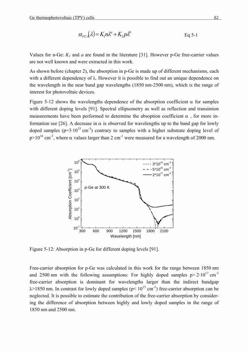
Ge thermophotovoltaic (TPV) cells 82
( ) baFCA pKnK λλλα 21 += Eq 5-1
Values for n-Ge: K1 and a are found in the literature [31]. However p-Ge free-carrier values are not well known and were extracted in this work.
As shown before (chapter 2), the absorption in p-Ge is made up of different mechanisms, each with a different dependency of λ. However it is possible to find out an unique dependence on the wavelength in the near band gap wavelengths (1850 nm-2500 nm), which is the range of interest for photovoltaic devices.
Figure 5-12X shows the wavelengths dependence of the absorption coefficient α for samples with different doping levels [91]. Spectral ellipsometry as well as reflection and transimion measurements have been performed to determine the absoption coefficient α , for more in-formation see [26]. A decrease in α is observed for wavelengths up to the band gap for lowly doped samples (p=3·1015 cm-3) contrary to samples with a higher substrate doping level of p>1016 cm-3, where α values larger than 2 cm-1 were measured for a wavelength of 2000 nm.
300 600 900 1200 1500 1800 210010-1
100
101
102
103
104
105
106 3*1015 cm-3
5*1016 cm-3
2*1017 cm-3
Abs
orpt
ion
Coe
ffici
ent [
cm-1]
Wavelength [nm]
p-Ge at 300 K
Figure 5-12: Absorption in p-Ge for different doping levels [91].
Free-carrier absorption for p-Ge was calculated in this work for the range between 1850 nm and 2500 nm with the following assumptions: For highly doped samples p> 2·1017 cm-3
free-carrier absorption is dominant for wavelengths larger than the indirect bandgap λ>1850 nm. In contrast for lowly doped samples (p< 1015 cm-3) free-carrier absorption can be neglected. It is possible to estimate the contribution of the free-carrier absorption by consider-ing the difference of absorption between highly and lowly doped samples in the range of 1850 nm and 2500 nm.
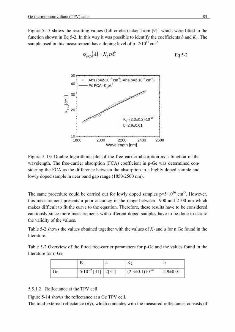
Ge thermophotovoltaic (TPV) cells 83
XFigure 5-13X shows the resulting values (full circles) taken from [91] which were fitted to the function shown in XEq 5-2X. In this way it was possible to identify the coefficients b and K2. The sample used in this measurement has a doping level of p=2·1017 cm-3.
( ) bFCA pK λλα 2= Eq 5-2
1800 2000 2200 2400 260010
20
30
40
50
K2=(2.3±0.2)·10-26
b=2.9±0.01
Wavelength [nm]
α FC
A[c
m-1]
Abs (p=2·1017 cm-3)-Abs(p=2·1015 cm-3) Fit FCA=K2pλb
Figure 5-13: Double logarithmic plot of the free carrier absorption as a function of the wavelength. The free-carrier absorption (FCA) coefficient in p-Ge was determined con-sidering the FCA as the difference between the absorption in a highly doped sample and lowly doped sample in near band gap range (1850-2500 nm).
The same procedure could be carried out for lowly doped samples p=5·1016 cm-3. However, this measurement presents a poor accuracy in the range between 1900 and 2100 nm which makes difficult to fit the curve to the equation. Therefore, these results have to be considered cautiously since more measurements with different doped samples have to be done to assure the validity of the values.
Table 5-2 shows the values obtained together with the values of K1 and a for n Ge found in the literature.
Table 5-2 Overview of the fitted free-carrier parameters for p-Ge and the values found in the literature for n-Ge
K1 a K2 b
Ge 5·10-25 [31] 2[31] (2.3±0.1)10-26 2.9±0.01
5.5.1.2 Reflectance at the TPV cell
Figure 5-14 shows the reflectance at a Ge TPV cell. The total external reflectance (RT), which coincides with the measured reflectance, consists of
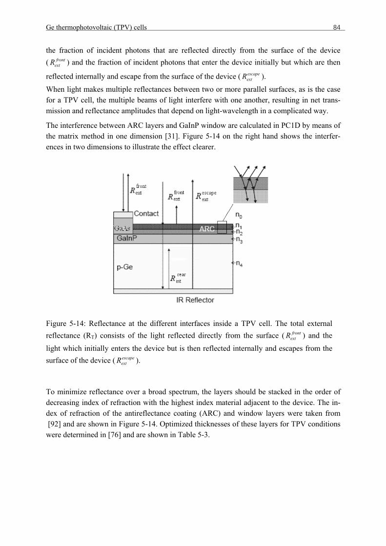
Ge thermophotovoltaic (TPV) cells 84
the fraction of incident photons that are reflected directly from the surface of the device ( front
extR ) and the fraction of incident photons that enter the device initially but which are then
reflected internally and escape from the surface of the device ( escapeextR ).
When light makes multiple reflectances between two or more parallel surfaces, as is the case for a TPV cell, the multiple beams of light interfere with one another, resulting in net trans-mission and reflectance amplitudes that depend on light-wavelength in a complicated way.
The interference between ARC layers and GaInP window are calculated in PC1D by means of the matrix method in one dimension [31]. Figure 5-14 on the right hand shows the interfer-ences in two dimensions to illustrate the effect clearer.
Figure 5-14: Reflectance at the different interfaces inside a TPV cell. The total external reflectance (RT) consists of the light reflected directly from the surface ( front
extR ) and the
light which initially enters the device but is then reflected internally and escapes from the surface of the device ( escape
extR ).
To minimize reflectance over a broad spectrum, the layers should be stacked in the order of decreasing index of refraction with the highest index material adjacent to the device. The in-dex of refraction of the antireflectance coating (ARC) and window layers were taken from [92] and are shown in XFigure 5-14. Optimized thicknesses of these layers for TPV conditions were determined in [76] and are shown in Table 5-3.
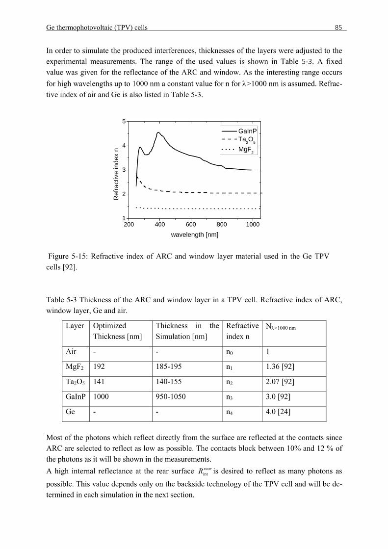
Ge thermophotovoltaic (TPV) cells 85
In order to simulate the produced interferences, thicknesses of the layers were adjusted to the experimental measurements. The range of the used values is shown in Table 5-3. A fixed value was given for the reflectance of the ARC and window. As the interesting range occurs for high wavelengths up to 1000 nm a constant value for n for λ>1000 nm is assumed. Refrac-tive index of air and Ge is also listed in Table 5-3.
200 400 600 800 10001
2
3
4
5R
efra
ctiv
e in
dex
n
wavelength [nm]
GaInP Ta2O5
MgF2
Figure 5-15: Refractive index of ARC and window layer material used in the Ge TPV cells [92].
Table 5-3 Thickness of the ARC and window layer in a TPV cell. Refractive index of ARC, window layer, Ge and air.
Layer Optimized Thickness [nm]
Thickness in the Simulation [nm]
Refractive index n
Nλ>1000 nm
Air - - n0 1
MgF2 192 185-195 n1 1.36 [92]
Ta2O5 141 140-155 n2 2.07 [92]
GaInP 1000 950-1050 n3 3.0 [92]
Ge - - n4 4.0 [24]
Most of the photons which reflect directly from the surface are reflected at the contacts since ARC are selected to reflect as low as possible. The contacts block between 10% and 12 % of the photons as it will be shown in the measurements. A high internal reflectance at the rear surface rearRint is desired to reflect as many photons as
possible. This value depends only on the backside technology of the TPV cell and will be de-termined in each simulation in the next section.
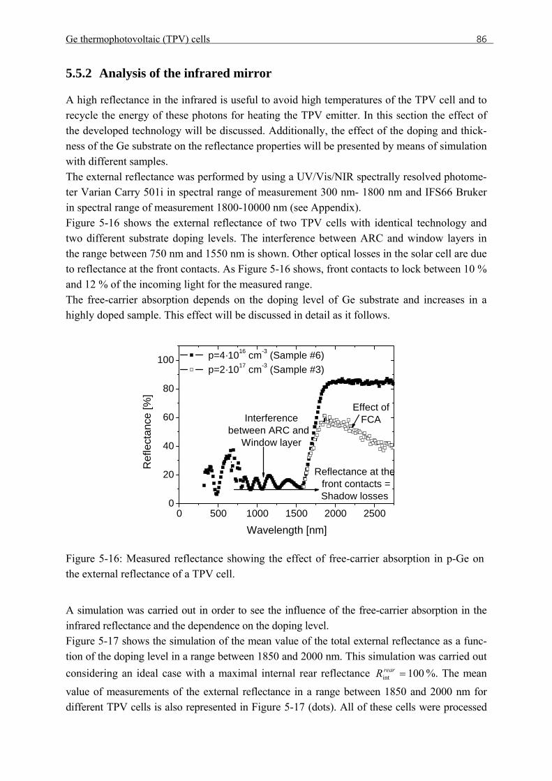
Ge thermophotovoltaic (TPV) cells 86
5.5.2 Analysis of the infrared mirror
A high reflectance in the infrared is useful to avoid high temperatures of the TPV cell and to recycle the energy of these photons for heating the TPV emitter. In this section the effect of the developed technology will be discussed. Additionally, the effect of the doping and thick-ness of the Ge substrate on the reflectance properties will be presented by means of simulation with different samples. The external reflectance was performed by using a UV/Vis/NIR spectrally resolved photome-ter Varian Carry 501i in spectral range of measurement 300 nm- 1800 nm and IFS66 Bruker in spectral range of measurement 1800-10000 nm (see Appendix). Figure 5-16X shows the external reflectance of two TPV cells with identical technology and two different substrate doping levels. The interference between ARC and window layers in the range between 750 nm and 1550 nm is shown. Other optical losses in the solar cell are due to reflectance at the front contacts. As Figure 5-16 shows, front contacts to lock between 10 % and 12 % of the incoming light for the measured range. The free-carrier absorption depends on the doping level of Ge substrate and increases in a highly doped sample. This effect will be discussed in detail as it follows.
0 500 1000 1500 2000 25000
20
40
60
80
100
Ref
lect
ance
[%]
Wavelength [nm]
p=4·1016 cm-3 (Sample #6) p=2·1017 cm-3 (Sample #3)
Effect of FCAInterference
between ARC and Window layer
Reflectance at the front contacts =Shadow losses
Figure 5-16: Measured reflectance showing the effect of free-carrier absorption in p-Ge on the external reflectance of a TPV cell.
A simulation was carried out in order to see the influence of the free-carrier absorption in the infrared reflectance and the dependence on the doping level. Figure 5-17 shows the simulation of the mean value of the total external reflectance as a func-tion of the doping level in a range between 1850 and 2000 nm. This simulation was carried out considering an ideal case with a maximal internal rear reflectance 100int =rearR %. The mean
value of measurements of the external reflectance in a range between 1850 and 2000 nm for different TPV cells is also represented in Figure 5-17 (dots). All of these cells were processed
Ge thermophotovoltaic (TPV) cells 87
with an identical optimized infrared mirror (Structure 2, see Figure 5-9), and a high value is expected for rearRint due to the polished back side surface and optimal infrared mirror.
For very low doping, most of the photons with high wavelength reach the back side and are reflected back without losses due to the very low free-carrier absorption. However, with a high doping level material, a fraction of these photons will be absorbed in the substrate. Figure 5-17 shows that the reflectivity in the infrared range decreases substantially when the substrate doping level is increased from p=4·1016 cm-3 to p=2·1017 cm-3. At a very high doping level (p>2·1018 cm-3) the front reflectance ( front
extR ) is uniquely responsible for the reflectance
at wavelengths higher than 1800 nm; photons which initially enter the device, do not escape from the surface of the device ( escape
extR =0) since everything is absorbed in Ge.
Using highly doped samples high free-carrier absorption is expected which results in a tem-perature increase in the cell. Since higher temperatures lead to lower voltage low free-carrier absorption is desirable and therefore it is necessary to choose a Ge substrate with a moderate doping level.
1015 1016 1017 1018 10190
20
40
60
80
100
Simulation Measurement
Ref
lect
ance
[%]
p-Ge Substrate doping level [cm-3]
R1
Average external reflectancebetween (1850 nm- 2000 nm)
Figure 5-17: Maximum external reflectance of photons between 1850 nm and 2000 nm at a TPV cell in dependence on the substrate doping level. The reflectance is the mean value between 1850 nm and 2000 nm. The substrate thickness is 150 µm.
Three different Ge TPV cells were measured and simulated using all the considerations ex-plained previously. Table 5-5X describes the Ge TPV cell structures. The back side of sam-ple #1 consists of evaporated TiPdAg whereas Sample #2 and #5 were processed with evapo-rated Aluminum . The back side of cells #3, #4, and #6 consist of a double layer of a-SixC1-x/SiO2 or a-Si/SiO2 covered with 2 µm of Al. In PC1D it is possible to select diffuse or specular reflectance. An infrared mirror which con-sists of a dielectric layer between Ge and the metal at a polished surface is expected to lead to specular reflectance. Otherwise a diffuse reflectance is expected in sample #1, which used TiPdAg evaporated directly onto a non polished Ge surface.
Ge thermophotovoltaic (TPV) cells 88
Table 5-4 shows the specification of these samples.
# Sample Doping Technology Thickness Mirror Polished back side 1 1844-4 2·1017 standard 150 TiPdAg No 2 1954-5-13 2·1017 1 150 Al Yes 3 1959-6_1 2·1017 2 150 a-Si /Al Yes 4 2713-4-14 2·1017 2 250 a-SixC1-x /Al Yes 5 2063-2 4·1016 1 150 Al Yes 6 2063-6-3 4·1016 2 150 a-Si /Al Yes
Reflectance of samples #1 and sample #3 were measured and simulated and are shown in XFigure 5-18. Both samples have the same doping level and thickness, and therefore similar losses due to free-carrier absorption. However they have different reflectance due to the dif-ferent technologies. Reflectance of sample #1 which consists of a back side of TiPdAg at a non polished back side was simulated choosing a diffuse internal rear reflectance of 13 %. A reflectance of 60 % was measured in sample #3 which was processed with the infrared mirror. To adjust the simulation to the measurement a value of an internal rear specular reflectance of 87 % was necessary. Sample #4 was also processed with the infraraed mirror, but in this case using a substrate thickness of 250 µm. Reflectance was also simulated and is shown on the right side of Figure 5-18. Sample #4 reflects less photons than sample #3 at the back side. Despite the higher thickness, photons which reach the back side and reflect back to the surface have more chances to be absorbed within the Ge substrate and therefore less chance to escape from the surface of the device ( escape
extR is lower).
400 800 1200 1600 2000
0
20
40
60
80
100
Rintrear=13% Diffuse
Sample #3 Infrared mirrora-Si/SiO2/Al
Sample #1 TiPdAg
Rintrear=87% Specular W=150 µm
Ref
lect
ance
[%]
Simulation Measurement
Wavelength [nm] 400 800 1200 1600 2000
0
20
40
60
80
100
Sample #4 Infrared mirrora-SixC1-x/SiO2/Al
Rintrear=85% Specular
W=250 µm
Simulation Measurement
Ref
lect
ance
[%]
Wavelength [nm]
Figure 5-18: Measurement and simulation of the reflectivity of TPV cells with highly doped substrates (2·1017 cm-3). Left: TPV cell with TiPdAg back side (Sample #1) and infrared reflector (Sample #3) on a substrate with a thickness of 150 µm. Right: infrared reflector (Sample #4) on a substrate with a thickness of 250 µm.
Reflectance of TPV cells with a substrate with a doping level of 4·1016 cm-3 are shown in XFigure 5-19X. Sample #6, with a suitable infrared back reflector, shows a reflectance higher
Ge thermophotovoltaic (TPV) cells 89
than 85 %. It is also close to the optimum with a simulated rear specular reflectance of rearRint = 93 %. Using aluminum at the back side, a reflectance of 60 % was achieved. In this
case a value of rearRint =65% was necessary to adjust the measurement to the simulation.
The infrared reflectance is limited by the doping and thickness of the substrate. Using the new back side technology developed in this work, a measured reflectance of 60% and 85% at low doping level of 2·1017 cm-3 and 4·1016 cm-3 was obtained respectively. Once the optical parameters are well-known it is possible to study the electrical properties of the surface passivation of the back side.
400 800 1200 1600 20000
20
40
60
80
100 Sample #6 Infrared mirrora-Si/SiO2/Al
Sample #5 Aluminum
Rintrear=65% Specular
Rintrear=93% Specular
W=150 µm
Simulation Measurement
Ref
lect
ance
[%]
Wavelength [nm]
Figure 5-19: Measurement and simulation results for reflectance of a TPV cell with a Ge doping level of 4·1016 cm-3 and an infrared back side mirror consisting of a-Si/SiO2/Al in the case of sample #6 and an evaporated Aluminum layer at the back side of sample #5.
5.5.3 Electrical parameters
Photons with wavelengths between 1550 nm and 2000 nm are absorbed within the p-Ge sub-strate. The photo response of the cell in this range is very sensitive to changes in the p-Ge properties like doping, thickness and the back side technology. To find the optimized Ge pa-rameters and back side technology was one of the main topics of this work and therefore a detailed study of p-Ge parameters used in the simulation is presented as follows.
Bulk lifetime in dependence on the doping level and intrinsic Auger and radiative recombina-tion were established in this work and presented in chapter 4 whereas band gap narrowing coefficients were taken from the literature [31].
5.5.3.1 Bulk lifetime as a function of the doping level
In chapter 4, the bulk lifetime of samples with different doping levels was extracted. The bulk lifetime (τBulk) dependence on the doping level NA was given by equation Eq 4-1. Values given in XTable 5-5X were determined in this work and presented in chapter 4.
Ge thermophotovoltaic (TPV) cells 90
Table 5-5 Bulk lifetime parameters used for the simulation of Ge TPV cells by PC1D.
Parameter p- Ge τo 3800 µs Nonset 2·1014cm-3 α -0.45
5.5.3.2 Band gap narrowing model
The band gap narrowing has a significant effect on p-Ge with a doping level higher than NA=1·1018 cm-3 [31].
In PC1D the following expression is given for the band gap narrowing ΔEV which depend-ences on the doping level NA
⎟⎠⎞
⎜⎝⎛=Δ
OnsetNSlopeE A
V ln Eq 5-5
Table 5-6 Band gap narrowing parameters used in PC1D for p-Ge [31].
Parameter p-type Ge Onset 1·1018 cm-3 Slope 23 meV
5.5.3.3 Bulk recombination
Auger and radiative recombination coefficients in p-Ge are required to properly compute re-combination in Ge. The extraction of these coefficients was discussed in chapter 4. The values given in the literature, together with the values determined in this work are shown in Table 5-7.
Table 5-7 Auger and radiative recombination coefficients in p-Ge found in the literature and determined in this work
Literature This work Cp 5.4·10-31cm6/s [73] 5·10-32cm6/s B 6·10-14cm3/s [24] 3·10-14cm3/s
It is necessary to point out that electrical parameters, such as the intrinsic recombination pa-rameters (Ca, Cp, Cn and B) and the surface recombination, are independent of the simulation of the reflectance parameters.
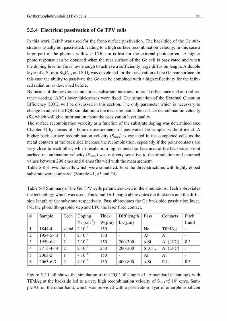
Ge thermophotovoltaic (TPV) cells 91
5.5.4 Electrical passivation of Ge TPV cells
In this work GaInP was used for the front-surface passivation. The back side of the Ge sub-strate is usually not passivated, leading to a high surface recombination velocity. In this case a large part of the photons with λ > 1550 nm is lost for the external photocurrent. A higher photo response can be obtained when the rear surface of the Ge cell is passivated and when the doping level in Ge is low enough to achieve a sufficiently large diffusion length. A double layer of a-Si or a-SixC1-x and SiO2 was developed for the passivation of the Ge rear surface. In this case the ability to passivate the Ge can be combined with a high reflectivity for the infra-red radiation as described before. By means of the previous simulations, substrate thickness, internal reflectance and anti reflec-tance coating (ARC) layer thicknesses were fixed. The simulation of the External Quantum Efficiency (EQE) will be discussed in this section. The only parameter which is necessary to change to adjust the EQE simulation to the measurement is the surface recombination velocity (S), which will give information about the passivation layer quality. The surface recombination velocity as a function of the substrate doping was determined (see Chapter 4) by means of lifetime measurements of passivated Ge samples without metal. A higher back surface recombination velocity (Sback) is expected in the completed cells as the metal contacts at the back side increase the recombination, especially if the point contacts are very close to each other, which results in a higher metal surface area at the back side. Front surface recombination velocity (Sfront) was not very sensitive to the simulation and assumed values between 200 cm/s and 0 cm/s fits well with the measurement. X Table 5-8 shows the cells which were simulated. First the three structures with highly doped substrate were compared (Sample #1, #3 and #4).
Table 5-8 Summary of the Ge TPV cells parameters used in the simulations. Tech abbreviates the technology which was used, Thick and Diff length abbreviates the thickness and the diffu-sion length of the substrate respectively. Pass abbreviates the Ge back side passivation layer, P-L the photolithographic step and LFC the laser fired contact.
# Sample Tech Doping NA (cm-3)
Thick W(µm)
Diff length LD (µm)
Pass Contacts Pitch (mm)
1 1844-4 stand 2·1017 150 - No TiPdAg - 2 1954-5-13 1 2·1017 150 - Al Al - 3 1959-6-1 2 2·1017 150 200-300 a-Si Al (LFC) 0.3 4 2713-4-14 2 2·1017 250 200-300 SixC1-x Al (LFC) 1 5 2063-2 1 4·1016 150 - Al Al - 6 2063-6-3 2 4·1016 150 400-800 a-Si P-L 0.3
XFigure 5-20 left shows the simulation of the EQE of sample #1. A standard technology with TiPdAg at the backside led to a very high recombination velocity of Sback=5·105 cm/s. Sam-ple #3, on the other hand, which was provided with a passivation layer of amorphous silicon
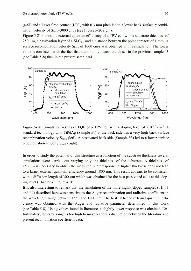
Ge thermophotovoltaic (TPV) cells 92
(a-Si) and a Laser fired contact (LFC) with 0.3 mm pitch led to a lower back surface recombi-nation velocity of Sback=3000 cm/s (see XFigure 5-20X right). Figure 5-21X shows the external quantum efficiency of a TPV cell with a substrate thickness of 250 µm, a passivation layer of a SixC1-x and a distance between the point contacts of 1 mm. A surface recombination velocity Sback of 1000 cm/s was obtained in this simulation. The lower value is consistent with the fact that aluminum contacts are closer in the previous sample #3 (see XTable 5-8) than in the present sample #4.
400 800 1200 1600 20000
20
40
60
80
100Sample #1
Standard TechnologyTiPdAg
Measurement Simulation
Sback=5·105 cm/s
EQ
E [%
]
Wavelength [nm]
Cp=5·10-32cm6/sW=150 µm
400 800 1200 1600 20000
20
40
60
80
100
Sback=5·105 cm/s
Technologie 2a-Si/SiO2/Al
Measurement Simulation
S=3000 cm/s
EQ
E [%
]
Wavelength [nm]
Sback=0 cm/s
Sample #3
Cp=5·10-32cm6/sW=150 µm
Figure 5-20: Simulation results of EQE of a TPV cell with a doping level of 2·1017 cm-3. A standard technology with TiPdAg (Sample #1) at the back side has a very high back surface recombination velocity Sback (left). A passivated back side (Sample #3) led to a lower surface recombination velocity Sback (right).
In order to study the potential of this structure as a function of the substrate thickness several simulations were carried out varying only the thickness of the substrate. A thickness of 250 µm is necessary to obtain the measured photoresponse. A higher thickness does not lead to a larger external quantum efficiency around 1800 nm. This result appears to be consistent with a diffusion length of 300 µm which was obtained for the best passivated cells at this dop-ing level (Chapter 4, Figure 4.20). It is also interesting to remark that the simulation of the more highly doped samples (#1, #3 and #4) described here was sensitive to the Auger recombination and radiative coefficient in the wavelength range between 1550 and 1600 nm. The best fit to the external quantum effi-ciency was obtained with the Auger and radiative parameter determined in this work (see XTable 5-8X). Using values found in literature, a slightly lower response was obtained. Un-fortunately, the error range is too high to make a serious distinction between the literature and present recombination coefficient data.
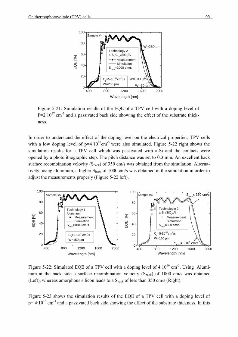
Ge thermophotovoltaic (TPV) cells 93
400 800 1200 1600 20000
20
40
60
80
100
W=100 µm
W=50 µm
Technology 2a-SixC1-x/SiO2/Al
Measurement Simulation
Sback=1000 cm/sEQ
E [%
]
Wavelength [nm]
Cp=5·10-32cm6/sW=250 µm
Sample #4
W>250 µm
Figure 5-21: Simulation results of the EQE of a TPV cell with a doping level of P=2·1017 cm-3 and a passivated back side showing the effect of the substrate thick-ness.
In order to understand the effect of the doping level on the electrical properties, TPV cells with a low doping level of p=4·1016cm-3 were also simulated. XFigure 5-22 right shows the simulation results for a TPV cell which was passivated with a-Si and the contacts were opened by a photolithographic step. The pitch distance was set to 0.3 mm. An excellent back surface recombination velocity (Sback) of 350 cm/s was obtained from the simulation. Alterna-tively, using aluminum, a higher Sback of 1000 cm/s was obtained in the simulation in order to adjust the measurements properly (Figure 5-22 left).
400 800 1200 1600 20000
20
40
60
80
100Sample #5
Technology 1Aluminum
Measurement Simulation
Sback=1000 cm/s
EQ
E [%
]
Wavelength [nm]
Cp=5·10-32cm6/s W=150 µm
400 800 1200 1600 20000
20
40
60
80
100
Cp=5·10-32cm6/s W=150 µm
Sback=5·105 cm/s
Technologie 2 a-Si /SiO2/Al
Measurement Simulation
Sback=350 cm/s
EQE
[%]
Wavelength [nm]
Sample #6 Sback< 350 cm/s
Figure 5-22: Simulated EQE of a TPV cell with a doping level of 4·1016 cm-3. Using Alumi-num at the back side a surface recombination velocity (Sback) of 1000 cm/s was obtained (Left), whereas amorphous silicon leads to a Sback of less than 350 cm/s (Right).
XFigure 5-23X shows the simulation results of the EQE of a TPV cell with a doping level of p= 4·1016 cm-3 and a passivated back side showing the effect of the substrate thickness. In this
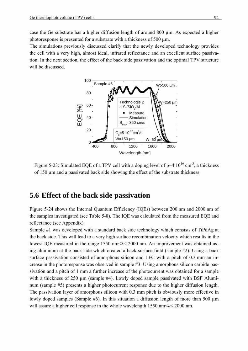
Ge thermophotovoltaic (TPV) cells 94
case the Ge substrate has a higher diffusion length of around 800 µm. As expected a higher photoresponse is presented for a substrate with a thickness of 500 µm. The simulations previously discussed clarify that the newly developed technology provides the cell with a very high, almost ideal, infrared reflectance and an excellent surface passiva-tion. In the next section, the effect of the back side passivation and the optimal TPV structure will be discussed.
400 800 1200 1600 20000
20
40
60
80
100
Cp=5·10-32cm6/sW=150 µm
W=250 µm
W>500 µm
Technologie 2a-Si/SiO2/Al
Measure Simulation
Sback=350 cm/sEQ
E [%
]
Wavelength [nm]
W=50 µm
Sample #6
Figure 5-23: Simulated EQE of a TPV cell with a doping level of p=4·1016 cm-3, a thickness of 150 µm and a passivated back side showing the effect of the substrate thickness
5.6 Effect of the back side passivation
Figure 5-24 shows the Internal Quantum Efficiency (IQEs) between 200 nm and 2000 nm of the samples investigated (see Table 5-8). The IQE was calculated from the measured EQE and reflectance (see Appendix). Sample #1 was developed with a standard back side technology which consists of TiPdAg at the back side. This will lead to a very high surface recombination velocity which results in the lowest IQE measured in the range 1550 nm<λ< 2000 nm. An improvement was obtained us-ing aluminum at the back side which created a back surface field (sample #2). Using a back surface passivation consisted of amorphous silicon and LFC with a pitch of 0.3 mm an in-crease in the photoresponse was observed in sample #3. Using amorphous silicon carbide pas-sivation and a pitch of 1 mm a further increase of the photocurrent was obtained for a sample with a thickness of 250 µm (sample #4). Lowly doped sample passivated with BSF Alumi-num (sample #5) presents a higher photocurrent response due to the higher diffusion length. The passivation layer of amorphous silicon with 0.3 mm pitch is obviously more effective in lowly doped samples (Sample #6). In this situation a diffusion length of more than 500 µm will assure a higher cell response in the whole wavelength 1550 nm<λ< 2000 nm.
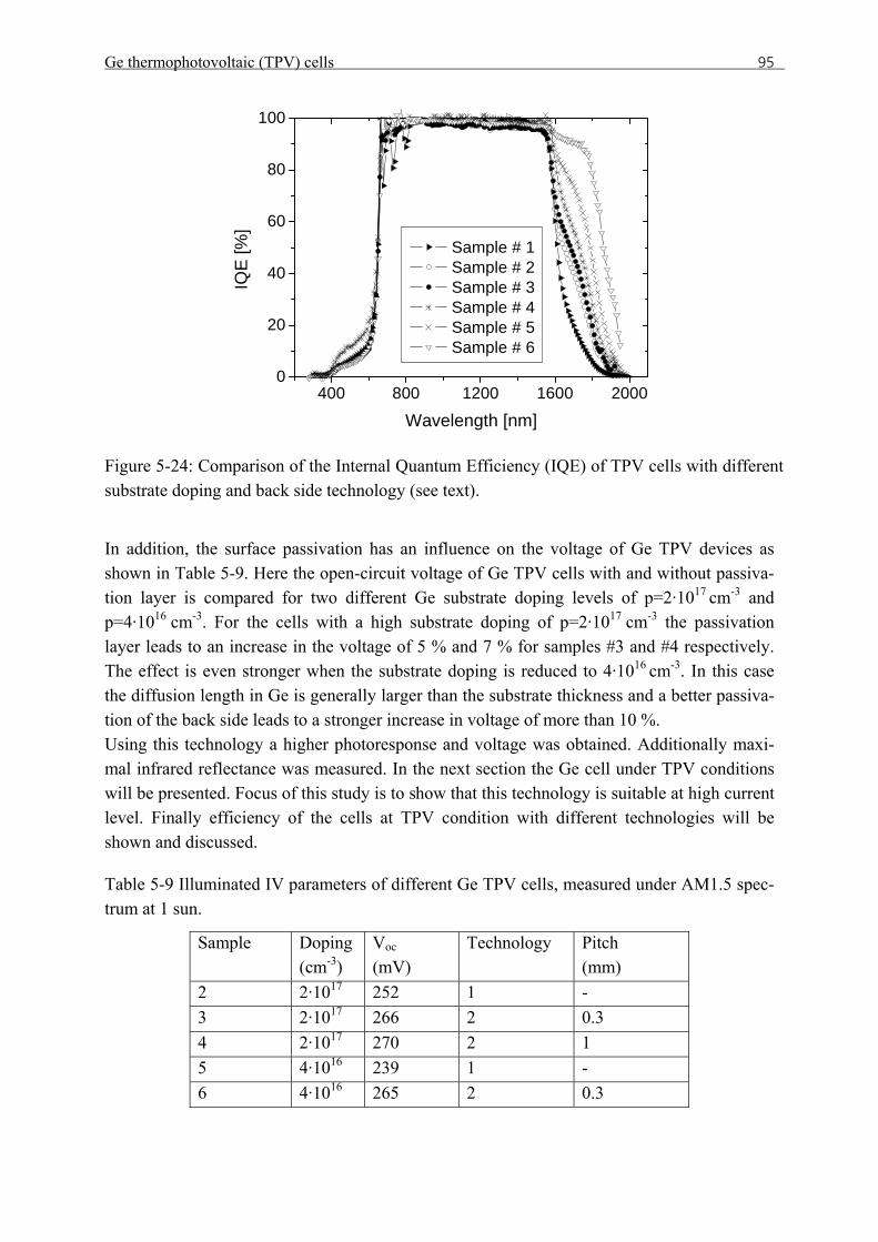
Ge thermophotovoltaic (TPV) cells 95
400 800 1200 1600 20000
20
40
60
80
100
IQE
[%]
Wavelength [nm]
Sample # 1 Sample # 2 Sample # 3 Sample # 4 Sample # 5 Sample # 6
Figure 5-24: Comparison of the Internal Quantum Efficiency (IQE) of TPV cells with different substrate doping and back side technology (see text).
In addition, the surface passivation has an influence on the voltage of Ge TPV devices as shown in XTable 5-9X. Here the open-circuit voltage of Ge TPV cells with and without passiva-tion layer is compared for two different Ge substrate doping levels of p=2·1017 cm-3 and p=4·1016 cm-3. For the cells with a high substrate doping of p=2·1017 cm-3 the passivation layer leads to an increase in the voltage of 5 % and 7 % for samples #3 and #4 respectively. The effect is even stronger when the substrate doping is reduced to 4·1016 cm-3. In this case the diffusion length in Ge is generally larger than the substrate thickness and a better passiva-tion of the back side leads to a stronger increase in voltage of more than 10 %. Using this technology a higher photoresponse and voltage was obtained. Additionally maxi-mal infrared reflectance was measured. In the next section the Ge cell under TPV conditions will be presented. Focus of this study is to show that this technology is suitable at high current level. Finally efficiency of the cells at TPV condition with different technologies will be shown and discussed.
Table 5-9 Illuminated IV parameters of different Ge TPV cells, measured under AM1.5 spec-trum at 1 sun.
Sample Doping (cm-3)
Voc
(mV) Technology Pitch
(mm) 2 2·1017 252 1 - 3 2·1017 266 2 0.3 4 2·1017 270 2 1 5 4·1016 239 1 - 6 4·1016 265 2 0.3
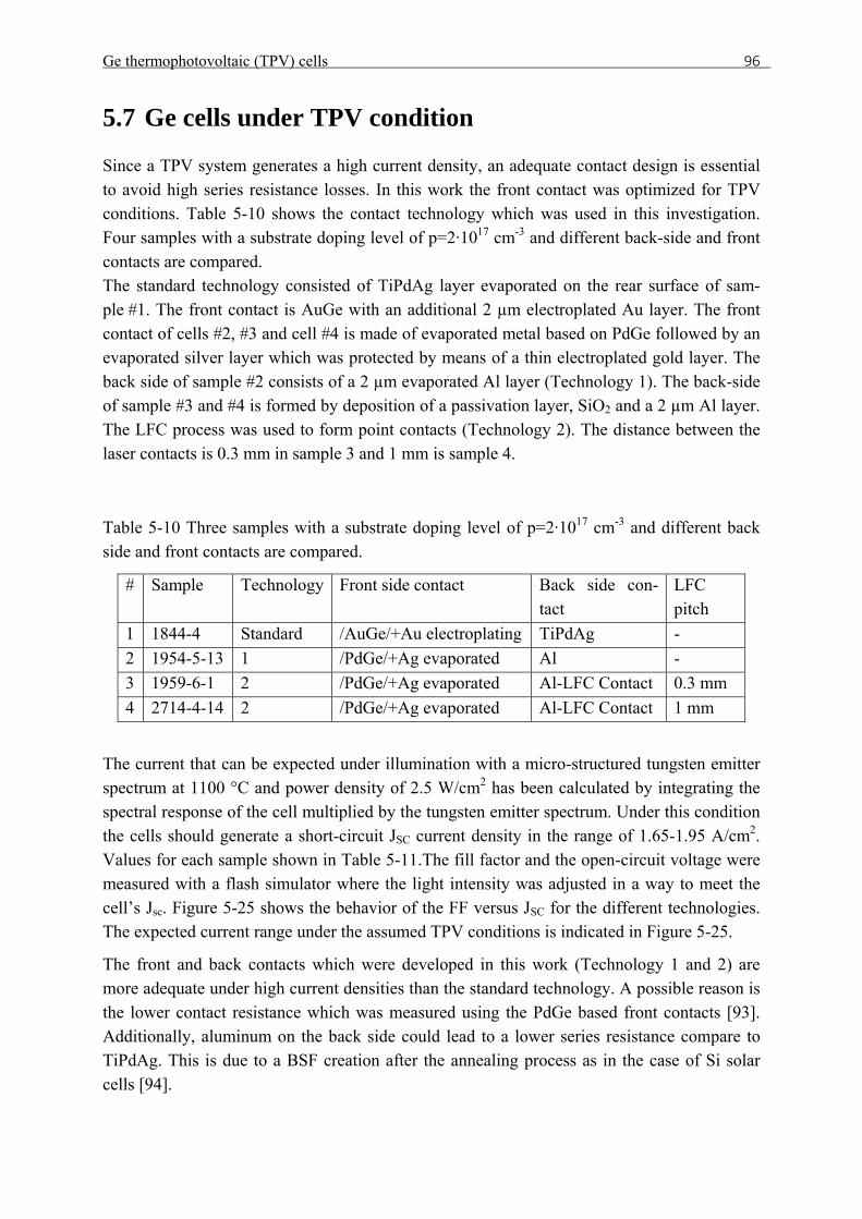
Ge thermophotovoltaic (TPV) cells 96
5.7 Ge cells under TPV condition
Since a TPV system generates a high current density, an adequate contact design is essential to avoid high series resistance losses. In this work the front contact was optimized for TPV conditions. Table 5-10 shows the contact technology which was used in this investigation. Four samples with a substrate doping level of p=2·1017 cm-3 and different back-side and front contacts are compared. The standard technology consisted of TiPdAg layer evaporated on the rear surface of sam-ple #1. The front contact is AuGe with an additional 2 µm electroplated Au layer. The front contact of cells #2, #3 and cell #4 is made of evaporated metal based on PdGe followed by an evaporated silver layer which was protected by means of a thin electroplated gold layer. The back side of sample #2 consists of a 2 µm evaporated Al layer (Technology 1). The back-side of sample #3 and #4 is formed by deposition of a passivation layer, SiO2 and a 2 µm Al layer. The LFC process was used to form point contacts (Technology 2). The distance between the laser contacts is 0.3 mm in sample 3 and 1 mm is sample 4.
Table 5-10 Three samples with a substrate doping level of p=2·1017 cm-3 and different back side and front contacts are compared.
# Sample Technology Front side contact Back side con-tact
LFC pitch
1 1844-4 Standard /AuGe/+Au electroplating TiPdAg - 2 1954-5-13 1 /PdGe/+Ag evaporated Al - 3 1959-6-1 2 /PdGe/+Ag evaporated Al-LFC Contact 0.3 mm 4 2714-4-14 2 /PdGe/+Ag evaporated Al-LFC Contact 1 mm
The current that can be expected under illumination with a micro-structured tungsten emitter spectrum at 1100 °C and power density of 2.5 W/cm2 has been calculated by integrating the spectral response of the cell multiplied by the tungsten emitter spectrum. Under this condition the cells should generate a short-circuit JSC current density in the range of 1.65-1.95 A/cm2. Values for each sample shown in Table 5-11.The fill factor and the open-circuit voltage were measured with a flash simulator where the light intensity was adjusted in a way to meet the cell’s Jsc. Figure 5-25 shows the behavior of the FF versus JSC for the different technologies. The expected current range under the assumed TPV conditions is indicated in Figure 5-25.
The front and back contacts which were developed in this work (Technology 1 and 2) are more adequate under high current densities than the standard technology. A possible reason is the lower contact resistance which was measured using the PdGe based front contacts [93]. Additionally, aluminum on the back side could lead to a lower series resistance compare to TiPdAg. This is due to a BSF creation after the annealing process as in the case of Si solar cells [94].
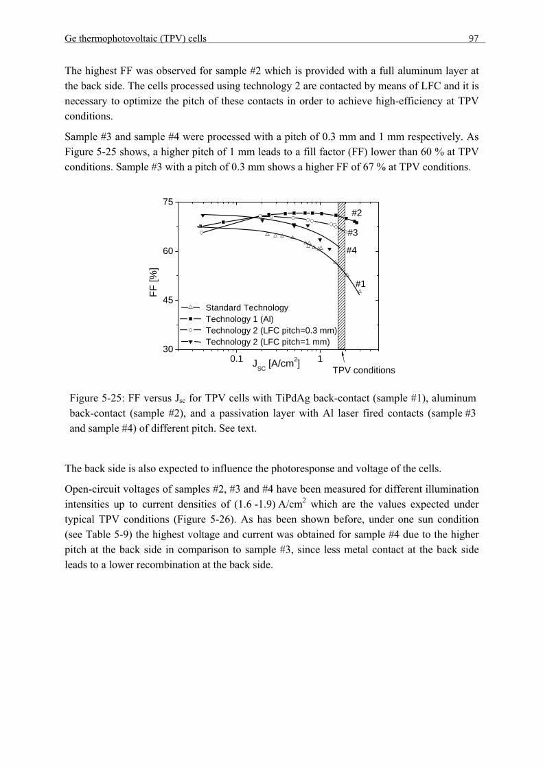
Ge thermophotovoltaic (TPV) cells 97
The highest FF was observed for sample #2 which is provided with a full aluminum layer at the back side. The cells processed using technology 2 are contacted by means of LFC and it is necessary to optimize the pitch of these contacts in order to achieve high-efficiency at TPV conditions.
Sample #3 and sample #4 were processed with a pitch of 0.3 mm and 1 mm respectively. As XFigure 5-25 shows, a higher pitch of 1 mm leads to a fill factor (FF) lower than 60 % at TPV conditions. Sample #3 with a pitch of 0.3 mm shows a higher FF of 67 % at TPV conditions.
0.1 130
45
60
75
#3
#4
#1
TPV conditions
FF [%
]
JSC [A/cm2]
Standard Technology Technology 1 (Al) Technology 2 (LFC pitch=0.3 mm) Technology 2 (LFC pitch=1 mm)
#2
Figure 5-25: FF versus Jsc for TPV cells with TiPdAg back-contact (sample #1), aluminum back-contact (sample #2), and a passivation layer with Al laser fired contacts (sample #3 and sample #4) of different pitch. See text.
The back side is also expected to influence the photoresponse and voltage of the cells.
Open-circuit voltages of samples #2, #3 and #4 have been measured for different illumination intensities up to current densities of (1.6 -1.9) A/cm2 which are the values expected under typical TPV conditions ( XFigure 5-26). As has been shown before, under one sun condition (see Table 5-9) the highest voltage and current was obtained for sample #4 due to the higher pitch at the back side in comparison to sample #3, since less metal contact at the back side leads to a lower recombination at the back side.
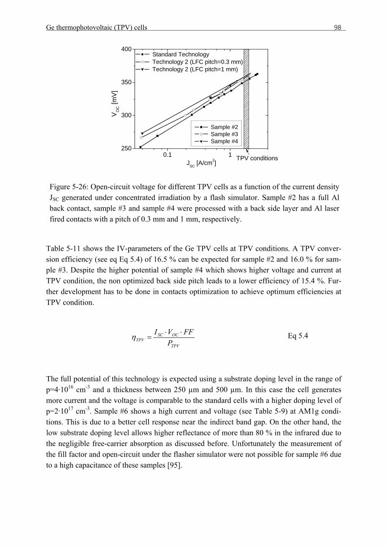
Ge thermophotovoltaic (TPV) cells 98
0.1 1250
300
350
400 Standard Technology Technology 2 (LFC pitch=0.3 mm) Technology 2 (LFC pitch=1 mm)
VO
C [m
V]
JSC [A/cm2]
Sample #2 Sample #3 Sample #4
TPV conditions
Figure 5-26: Open-circuit voltage for different TPV cells as a function of the current density JSC generated under concentrated irradiation by a flash simulator. Sample #2 has a full Al back contact, sample #3 and sample #4 were processed with a back side layer and Al laser fired contacts with a pitch of 0.3 mm and 1 mm, respectively.
Table 5-11 shows the IV-parameters of the Ge TPV cells at TPV conditions. A TPV conver-sion efficiency (see eq Eq 5.4) of 16.5 % can be expected for sample #2 and 16.0 % for sam-ple #3. Despite the higher potential of sample #4 which shows higher voltage and current at TPV condition, the non optimized back side pitch leads to a lower efficiency of 15.4 %. Fur-ther development has to be done in contacts optimization to achieve optimum efficiencies at TPV condition.
TPV
OCSCTPV P
FFVI ⋅⋅=η Eq 5.4
The full potential of this technology is expected using a substrate doping level in the range of p=4·1016 cm-3 and a thickness between 250 µm and 500 µm. In this case the cell generates more current and the voltage is comparable to the standard cells with a higher doping level of p=2·1017 cm-3. Sample #6 shows a high current and voltage (see Table 5-9) at AM1g condi-tions. This is due to a better cell response near the indirect band gap. On the other hand, the low substrate doping level allows higher reflectance of more than 80 % in the infrared due to the negligible free-carrier absorption as discussed before. Unfortunately the measurement of the fill factor and open-circuit under the flasher simulator were not possible for sample #6 due to a high capacitance of these samples [95].
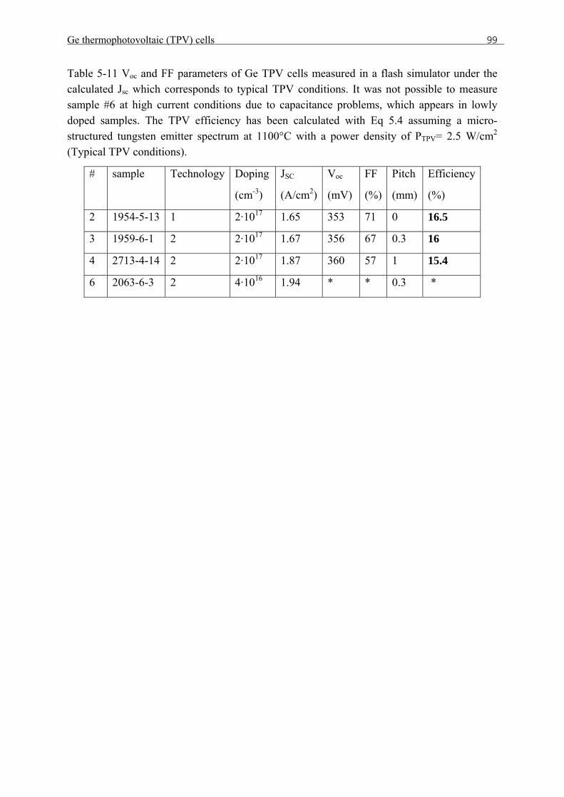
Ge thermophotovoltaic (TPV) cells 99
Table 5-11 Voc and FF parameters of Ge TPV cells measured in a flash simulator under the calculated Jsc which corresponds to typical TPV conditions. It was not possible to measure sample #6 at high current conditions due to capacitance problems, which appears in lowly doped samples. The TPV efficiency has been calculated with Eq 5.4 assuming a micro-structured tungsten emitter spectrum at 1100°C with a power density of PTPV= 2.5 W/cm2 (Typical TPV conditions).
# sample Technology Doping
(cm-3)
JSC
(A/cm2)
Voc
(mV)
FF
(%)
Pitch
(mm)
Efficiency
(%)
2 1954-5-13 1 2·1017 1.65 353 71 0 16.5
3 1959-6-1 2 2·1017 1.67 356 67 0.3 16
4 2713-4-14 2 2·1017 1.87 360 57 1 15.4
6 2063-6-3 2 4·1016 1.94 * * 0.3 *

Ge thermophotovoltaic (TPV) cells 100
Ge substrate optimization in triple-junction solar cells under space conditions 101
6 Ge substrate optimization in triple-junction solar cells under space conditions
In this section, Ge substrates have been optimized for metamorphic triple-
junction solar cells under space conditions by means of a new back side tech-
nology. Simulations have been carried out in order to understand the influ-
ence of the Ge substrate specifications and to obtain the maximum improve-
ment using the new technology. Finally, results of solar cells will be presented
and discussed.
6.1 Introduction
The III-V multi-junction solar cell structure, which is today commonly used for space applica-tions, is based on a lattice-matched material combination of Ga0.5In0.5P, Ga0.99In0.01As and Ge for the absorber layers. In this solar cell, the Ge sub-cell generates approximately 1.9 times the current density of the two other sub cells (see Figure 6-1 left). Therefore, an improvement of the Ge cell current does not necessarily lead to a better overall device performance. For this reason, the improvement of the Ge sub cell for higher efficiencies has not yet been a focus of R&D in this field. However, recently, lattice-mismatched structures have also been investi-gated due to their higher theoretical efficiency potential compared to the lattice-matched ma-terial combination. For these metamorphic structures, the current of the Ge bottom cell de-pends on the Indium content in the Ga1-xInxAs middle cell. In the case of Ga0.35In0.65P/Ga0.83In0.17As/Ge, the currents generated by all three sub-cells under AM0 condi-tions are nearly equal (see Figure 6-1 right). Therefore, these structures can directly benefit from a higher current of the Ge cell. Efforts were focused on the optimization of the top and middle solar cells [8] and the bottom cell was mostly ignored. Therefore, an analysis of the potential in Ge as an active part of the cell is necessary. Advanced concepts and technologies have been developed in this work in order to take the best advantage from Ge as a bottom cell. To reach this goal, the Ge rear surface has to be im-proved by a high quality surface passivation with low interface recombination velocity. Addi-tionally, the Ge substrate needs to have a low enough doping level to achieve sufficiently high bulk carrier lifetimes. In this case, the current generated in the indirect absorption range of Ge can be significantly improved as was shown in Ge single TPV cells (Chapter 5). Surface pas-sivation of Ge solar cells has up to now only been investigated for thermophotovoltaic (TPV) applications. In this work Ge TPV cell technology was adapted for the use in multi-junction space solar cells. The rear side of the Ge substrate was passivated by amorphous silicon car-bide (a-SixC1-x) to achieve a high external quantum efficiency between 1550 –2000 nm. At the same time, the a- SixC1-x passivation layer was used as part of a multi-layer back surface infra-red reflector which consists of a- SixC1-x, SiO2 and Al layers. The back side technology used for triple-junction solar cells is identical to the technology described in chapter 5 for single solar cells and will be here, therefore, only briefly presented.

Ge substrate optimization in triple-junction solar cells under space conditions 102
After that, simulations will be carried out in order to find out the suitable parameters which lead to the highest possible efficiency in Ge considering an ideal metamorphic structure where all the cells have the same current. Finally, the results of the cells which were processed in this work will be presented and discussed.
Lattice-matched
ηtheoretical=41.9%
Metamorphic
ηtheoretical=45.2%
Figure 6-1: Lattice matched and metamorphic triple-junction solar cells. Current distribu-tion under AM0 for top, middle and bottom cells.
6.2 Back side technology optimization
Lattice-matched and metamorphic Ga1-yInyP/Ga1-xInxAs/Ge triple-junction solar cell structures were grown by metal organic vapor phase epitaxy on an AIX2600-G3 reactor with a 8x4-inch configuration. Typical source materials include TMGa, TMIn, TMAl, DMZn, DETe, CBr4, AsH3 and PH3. Ge wafers with <100> orientation 6° off towards <111> were used. The stan-dard wafers had lapped and etched back sides and the wafers for cells with infrared reflector were polished on both sides. The Ge substrate doping level was chosen to be in the range of p=(2-20)·1016 cm-3 with a thickness of 250 µm. A 100-200 nm thick n-type emitter was formed by phosphorous diffusion into Ge, which led to a surface carrier concentration of n>5·1018 cm-3 [88]. The Ge front surface passivation is achieved by an epitaxially grown n-GaInP or GaInAs window layer with a high doping level of n> 1018 cm-3 (see Figure 6-2). Standard solar cell devices with an area of 4 cm2 were processed with planar metal contacts made of 2 µm aluminum on the rear side. Identical structures were also processed with an a SixC1-x passivation layer, followed by a SiO2 layer and 2 µm of Al with point contacts to the Ge base (see Figure 6-3). The a-SixC1-x multi-layer structure for the back side passivation and the infrared reflector were deposited by PECVD (plasma enhanced chemical vapor deposi-tion). The preconditioning of the Ge substrates before the deposition of a-SixC1-x and SiO2, as
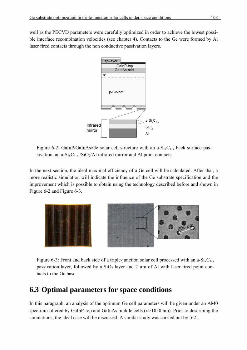
Ge substrate optimization in triple-junction solar cells under space conditions 103
well as the PECVD parameters were carefully optimized in order to achieve the lowest possi-ble interface recombination velocities (see chapter 4). Contacts to the Ge were formed by Al laser fired contacts through the non conductive passivation layers.
Figure 6-2: GaInP/GaInAs/Ge solar cell structure with an a-SixC1-x back surface pas-sivation, an a-SixC1-x /SiO2/Al infrared mirror and Al point contacts
In the next section, the ideal maximal efficiency of a Ge cell will be calculated. After that, a more realistic simulation will indicate the influence of the Ge substrate specification and the improvement which is possible to obtain using the technology described before and shown in Figure 6-2 and Figure 6-3.
Figure 6-3: Front and back side of a triple-junction solar cell processed with an a-SixC1-x passivation layer, followed by a SiO2 layer and 2 µm of Al with laser fired point con-tacts to the Ge base.
6.3 Optimal parameters for space conditions
In this paragraph, an analysis of the optimum Ge cell parameters will be given under an AM0 spectrum filtered by GaInP-top and GaInAs middle cells (λ>1050 nm). Prior to describing the simulations, the ideal case will be discussed. A similar study was carried out by [62].
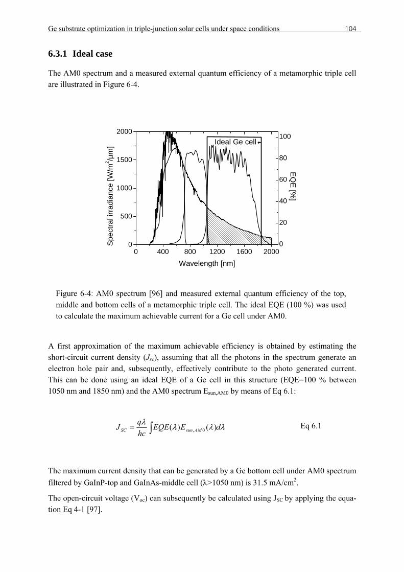
Ge substrate optimization in triple-junction solar cells under space conditions 104
6.3.1 Ideal case
The AM0 spectrum and a measured external quantum efficiency of a metamorphic triple cell are illustrated in Figure 6-4.
0 400 800 1200 1600 20000
500
1000
1500
2000
0
20
40
60
80
100
EQ
E [%
]Sp
ectra
l irra
dian
ce [W
/m2 /µ
m]
Wavelength [nm]
Ideal Ge cell
Figure 6-4: AM0 spectrum [96] and measured external quantum efficiency of the top, middle and bottom cells of a metamorphic triple cell. The ideal EQE (100 %) was used to calculate the maximum achievable current for a Ge cell under AM0.
A first approximation of the maximum achievable efficiency is obtained by estimating the short-circuit current density (Jsc), assuming that all the photons in the spectrum generate an electron hole pair and, subsequently, effectively contribute to the photo generated current. This can be done using an ideal EQE of a Ge cell in this structure (EQE=100 % between 1050 nm and 1850 nm) and the AM0 spectrum Esun,AM0 by means of Eq 6.1:
λλλλ dEEQEhcqJ AMsunSC ∫= )()( 0, Eq 6.1
The maximum current density that can be generated by a Ge bottom cell under AM0 spectrum filtered by GaInP-top and GaInAs-middle cell (λ>1050 nm) is 31.5 mA/cm2.
The open-circuit voltage (Voc) can subsequently be calculated using JSC by applying the equa-tion Eq 4-1 [97].
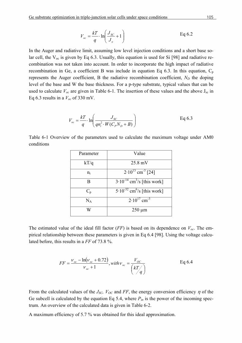
Ge substrate optimization in triple-junction solar cells under space conditions 105
⎟⎟⎠
⎞⎜⎜⎝
⎛+⋅= 1ln
o
SCoc J
Jq
kTV Eq 6.2
In the Auger and radiative limit, assuming low level injection conditions and a short base so-lar cell, the Voc is given by Eq 6.3. Usually, this equation is used for Si [98] and radiative re-combination was not taken into account. In order to incorporate the high impact of radiative recombination in Ge, a coefficient B was include in equation Eq 6.3. In this equation, Cp represents the Auger coefficient, B the radiative recombination coefficient, ND the doping level of the base and W the base thickness. For a p-type substrate, typical values that can be used to calculate Voc are given in Table 6-1. The insertion of these values and the above Jsc in Eq 6.3 results in a Voc of 330 mV.
⎟⎟⎠
⎞⎜⎜⎝
⎛+⋅
⋅=)(
ln 2 BNCWqnJ
qkTV
DPi
SCoc Eq 6.3
Table 6-1 Overview of the parameters used to calculate the maximum voltage under AM0 conditions
Parameter Value
kT/q 25.8 mV
ni 2·1013 cm-3 [24]
B 3·10-14 cm3/s [this work]
Cp 5·10-32 cm6/s [this work]
NA 2·1017 cm-3
W 250 µm
The estimated value of the ideal fill factor (FF) is based on its dependence on Voc. The em-pirical relationship between these parameters is given in Eq 6.4 [98]. Using the voltage calcu-lated before, this results in a FF of 73.8 %.
( )⎟⎠⎞⎜
⎝⎛
=+
+−=
qkTV
withFF OCoc
oc
ococ νν
νν,
172.0ln
Eq 6.4
From the calculated values of the JSC, VOC and FF, the energy conversion efficiency η of the Ge subcell is calculated by the equation Eq 5.4, where Pin is the power of the incoming spec-trum. An overview of the calculated data is given in Table 6-2.
A maximum efficiency of 5.7 % was obtained for this ideal approximation.
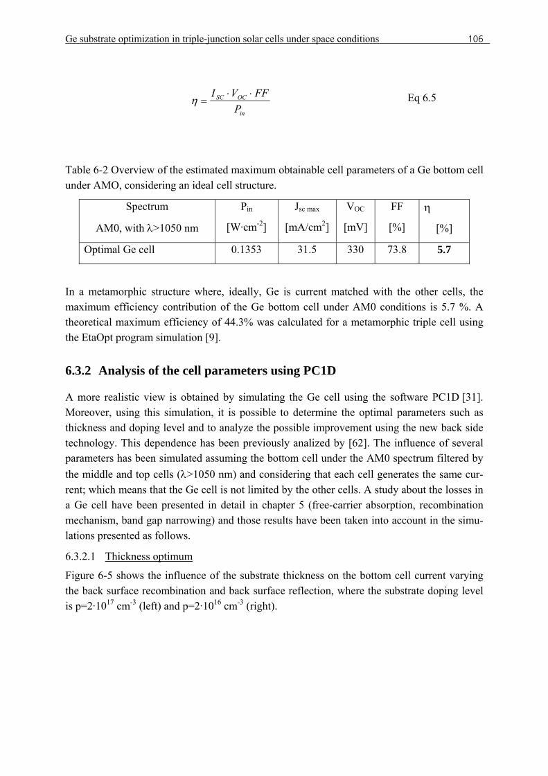
Ge substrate optimization in triple-junction solar cells under space conditions 106
in
OCSC
PFFVI ⋅⋅
=η Eq 6.5
Table 6-2 Overview of the estimated maximum obtainable cell parameters of a Ge bottom cell under AMO, considering an ideal cell structure.
Spectrum
AM0, with λ>1050 nm
Pin
[W·cm-2]
Jsc max
[mA/cm2]
VOC
[mV]
FF
[%]
η
[%]
Optimal Ge cell 0.1353 31.5 330 73.8 5.7
In a metamorphic structure where, ideally, Ge is current matched with the other cells, the maximum efficiency contribution of the Ge bottom cell under AM0 conditions is 5.7 %. A theoretical maximum efficiency of 44.3% was calculated for a metamorphic triple cell using the EtaOpt program simulation [9].
6.3.2 Analysis of the cell parameters using PC1D
A more realistic view is obtained by simulating the Ge cell using the software PC1D [31]. Moreover, using this simulation, it is possible to determine the optimal parameters such as thickness and doping level and to analyze the possible improvement using the new back side technology. This dependence has been previously analized by [62]. The influence of several parameters has been simulated assuming the bottom cell under the AM0 spectrum filtered by the middle and top cells (λ>1050 nm) and considering that each cell generates the same cur-rent; which means that the Ge cell is not limited by the other cells. A study about the losses in a Ge cell have been presented in detail in chapter 5 (free-carrier absorption, recombination mechanism, band gap narrowing) and those results have been taken into account in the simu-lations presented as follows.
6.3.2.1 Thickness optimum
Figure 6-5 shows the influence of the substrate thickness on the bottom cell current varying the back surface recombination and back surface reflection, where the substrate doping level is p=2·1017 cm-3 (left) and p=2·1016 cm-3 (right).
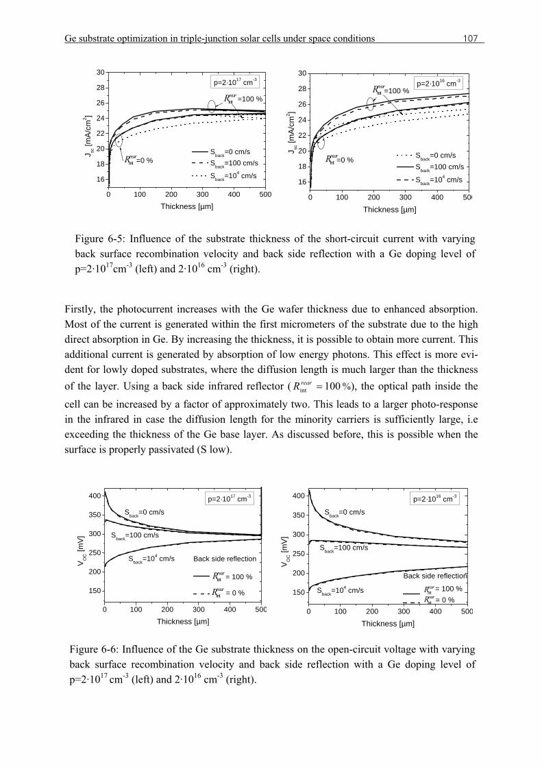
Ge substrate optimization in triple-junction solar cells under space conditions 107
0 100 200 300 400 500
16
18
20
22
24
26
28
30
=0 % rearRint
rearRint
Sback=0 cm/s Sback=100 cm/s
Sback=104 cm/s
p=2·1017 cm-3
J sc [m
A/cm
2 ]
Thickness [µm]
=100 %
0 100 200 300 400 500
16
18
20
22
24
26
28
30
Sback=0 cm/s Sback=100 cm/s
Sback=104 cm/s
J sc [m
A/c
m2 ]
=100 %
=0 % rearRint
rearRintp=2·1016 cm-3
Thickness [µm]
Figure 6-5: Influence of the substrate thickness of the short-circuit current with varying back surface recombination velocity and back side reflection with a Ge doping level of p=2·1017cm-3 (left) and 2·1016 cm-3 (right).
Firstly, the photocurrent increases with the Ge wafer thickness due to enhanced absorption. Most of the current is generated within the first micrometers of the substrate due to the high direct absorption in Ge. By increasing the thickness, it is possible to obtain more current. This additional current is generated by absorption of low energy photons. This effect is more evi-dent for lowly doped substrates, where the diffusion length is much larger than the thickness of the layer. Using a back side infrared reflector ( 100int =rearR %), the optical path inside the
cell can be increased by a factor of approximately two. This leads to a larger photo-response in the infrared in case the diffusion length for the minority carriers is sufficiently large, i.e exceeding the thickness of the Ge base layer. As discussed before, this is possible when the surface is properly passivated (S low).
0 100 200 300 400 500
150
200
250
300
350
400
= 0 % rearRint
rearRint
Sback=104 cm/s
Sback=100 cm/s
Sback=0 cm/s
Back side reflection
p=2·1017 cm-3
VO
C [m
V]
Thickness [µm]
= 100 %
0 100 200 300 400 500
150
200
250
300
350
400
rearRintSback=104 cm/s
Sback=100 cm/s
Sback=0 cm/s
p=2·1016 cm-3
V OC [m
V]
Thickness [µm]
= 0 % rearRint
Back side reflection
= 100 %
Figure 6-6: Influence of the Ge substrate thickness on the open-circuit voltage with varying back surface recombination velocity and back side reflection with a Ge doping level of p=2·1017 cm-3 (left) and 2·1016 cm-3 (right).
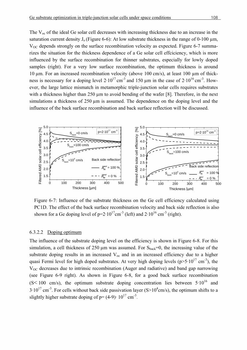
Ge substrate optimization in triple-junction solar cells under space conditions 108
The Voc of the ideal Ge solar cell decreases with increasing thickness due to an increase in the saturation current density Jo (Figure 6-6): At low substrate thickness in the range of 0-100 µm, VOC depends strongly on the surface recombination velocity as expected. Figure 6-7 summa-rizes the situation for the thickness dependence of a Ge solar cell effciciency, which is more influenced by the surface recombination for thinner substrates, especially for lowly doped samples (right). For a very low surface recombination, the optimum thickness is around 10 µm. For an increased recombination velocity (above 100 cm/s), at least 100 µm of thick-ness is necessary for a doping level 2·1017 cm-3 and 150 µm in the case of 2·1016 cm-3. How-ever, the large lattice mismatch in metamorphic triple-junction solar cells requires substrates with a thickness higher than 250 µm to avoid bending of the wafer [8]. Therefore, in the next simulations a thickness of 250 µm is assumed. The dependence on the doping level and the influence of the back surface recombination and back surface reflection will be discussed.
0 100 200 300 400 500
1.5
2.0
2.5
3.0
3.5
4.0
4.5
5.0
Sback=104 cm/s
Sback=100 cm/s
Filte
red
AM
0 so
lar c
ell e
ffici
ency
[%]
Thickness [µm]
p=2·1017 cm-3Sback=0 cm/s
= 0 % rearRint
rearRint
Back side reflection
= 100 %
0 100 200 300 400 500
1.5
2.0
2.5
3.0
3.5
4.0
4.5
5.0
Sback=104 cm/s
Sback=100 cm/s
Sback=0 cm/sFi
ltere
d AM
0 so
lar c
ell e
ffici
ency
[%
]
Thickness [µm]
p=2·1016 cm-3
rearRint
= 0 % rearRint
Back side reflection
= 100 %
Figure 6-7: Influence of the substrate thickness on the Ge cell efficiency calculated using PC1D. The effect of the back surface recombination velocity and back side reflection is also shown for a Ge doping level of p=2·1017cm-3 (left) and 2·1016 cm-3 (right).
6.3.2.2 Doping optimum
The influence of the substrate doping level on the efficiency is shown in Figure 6-8. For this simulation, a cell thickness of 250 µm was assumed. For Sback=0, the increasing value of the substrate doping results in an increased Voc and in an increased efficiency due to a higher quasi Fermi level for high doped substrates. At very high doping levels (p>5·1017 cm-3), the VOC decreases due to intrinsic recombination (Auger and radiative) and band gap narrowing (see Figure 6-9 right). As shown in Figure 6-8, for a good back surface recombination (S< 100 cm/s), the optimum substrate doping concentration lies between 5·1016 and 3·1017 cm-3. For cells without back side passivation layer (S>104cm/s), the optimum shifts to a slightly higher substrate doping of p= (4-9)· 1017 cm-3.
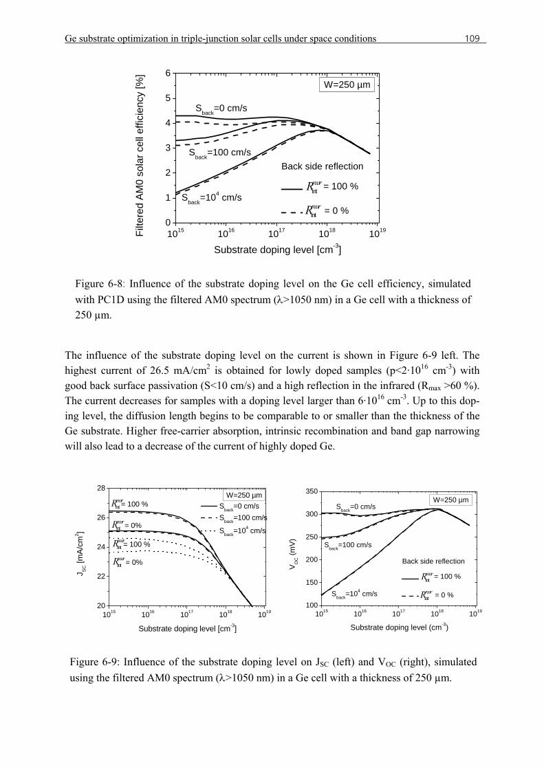
Ge substrate optimization in triple-junction solar cells under space conditions 109
The influence of the substrate doping level on the current is shown in Figure 6-9 left. The highest current of 26.5 mA/cm2 is obtained for lowly doped samples (p<2·1016 cm-3) with good back surface passivation (S<10 cm/s) and a high reflection in the infrared (Rmax >60 %). The current decreases for samples with a doping level larger than 6·1016 cm-3. Up to this dop-ing level, the diffusion length begins to be comparable to or smaller than the thickness of the Ge substrate. Higher free-carrier absorption, intrinsic recombination and band gap narrowing will also lead to a decrease of the current of highly doped Ge.
1015 1016 1017 1018 101920
22
24
26
28
= 0%
= 100 %
rearRint
rearRint
W=250 µm Sback=0 cm/s Sback=100 cm/s
Sback=104 cm/s
J SC [m
A/cm
2 ]
Substrate doping level [cm-3]
= 100 % rearRint
= 0% rearRint
1015 1016 1017 1018 1019100
150
200
250
300
350W=250 µm
Sback=104 cm/s
Sback=100 cm/s
Sback=0 cm/s
VO
C (m
V)
Substrate doping level (cm-3)
= 0 % rearRint
rearRint
Back side reflection
= 100 %
Figure 6-9: Influence of the substrate doping level on JSC (left) and VOC (right), simulated using the filtered AM0 spectrum (λ>1050 nm) in a Ge cell with a thickness of 250 µm.
1015 1016 1017 1018 10190
1
2
3
4
5
6W=250 µm
Sback=104 cm/s
Sback=100 cm/s
Sback=0 cm/s
Filte
red
AM
0 so
lar c
ell e
ffici
ency
[%]
Substrate doping level [cm-3]
= 0 % rearRint
rearRint
Back side reflection
= 100 %
Figure 6-8: Influence of the substrate doping level on the Ge cell efficiency, simulated with PC1D using the filtered AM0 spectrum (λ>1050 nm) in a Ge cell with a thickness of 250 µm.
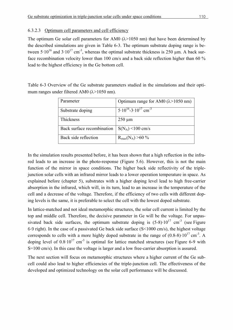
Ge substrate optimization in triple-junction solar cells under space conditions 110
6.3.2.3 Optimum cell parameters and cell efficiency
The optimum Ge solar cell parameters for AM0 (λ>1050 nm) that have been determined by the described simulations are given in Table 6-3. The optimum substrate doping range is be-tween 5·1016 and 3·1017 cm-3, whereas the optimal substrate thickness is 250 µm. A back sur-face recombination velocity lower than 100 cm/s and a back side reflection higher than 60 % lead to the highest efficiency in the Ge bottom cell.
Table 6-3 Overview of the Ge substrate parameters studied in the simulations and their opti-mum ranges under filtered AM0 (λ>1050 nm).
Parameter Optimum range for AM0 (λ>1050 nm)
Substrate doping 5·1016-3·1017 cm-3
Thickness 250 µm
Back surface recombination S(NA) <100 cm/s
Back side reflection Rmax(NA) >60 %
In the simulation results presented before, it has been shown that a high reflection in the infra-red leads to an increase in the photo-response (Figure 5.6). However, this is not the main function of the mirror in space conditions. The higher back side reflectivity of the triple-junction solar cells with an infrared mirror leads to a lower operation temperature in space. As explained before (chapter 5), substrates with a higher doping level lead to high free-carrier absorption in the infrared, which will, in its turn, lead to an increase in the temperature of the cell and a decrease of the voltage. Therefore, if the efficiency of two cells with different dop-ing levels is the same, it is preferable to select the cell with the lowest doped substrate.
In lattice-matched and not ideal metamorphic structures, the solar cell current is limited by the top and middle cell. Therefore, the decisive parameter in Ge will be the voltage. For unpas-sivated back side surfaces, the optimum substrate doping is (5-8)·1017 cm-3 (see Figure
6-9 right). In the case of a passivated Ge back side surface (S<1000 cm/s), the highest voltage corresponds to cells with a more highly doped substrate in the range of (0.8-8)·1017 cm-3. A doping level of 0.8·1017 cm-3 is optimal for lattice matched structures (see Figure 6-9 with S=100 cm/s). In this case the voltage is larger and a low free-carrier absorption is assured.
The next section will focus on metamorphic structures where a higher current of the Ge sub-cell could also lead to higher efficiencies of the triple-junction cell. The effectiveness of the developed and optimized technology on the solar cell performance will be discussed.
Ge substrate optimization in triple-junction solar cells under space conditions 111
6.4 Results and discussion
Three different metamorphic triple-junction solar cells were processed in this work with a p-Ge substrate with a thickness of 250 µm and specifications shown in Table 6-4. A substrate with a doping level of 2·1017 cm-3 was used for sample #1, whereas a doping level of 2·1016 cm-3 was used in samples #2 and #3. The back side of samples #1 and sample #2 con-sists of evaporated aluminum (Technology 1), whereas the back side of cells #3 consists of a double layer of a-SixC1-x/SiO2, followed by 2 µm of Al and contacted by means of laser fired contacts (Technology 2).
Table 6-4 Overview of the substrate specifications of three metamorphic triple-junction cells processed in this work
# Sample Tech p-Doping IR-Reflector Pass Back con-tact
1 2742-3-4g 1 2·1017 cm-3 Al Al (BSF) Al
2 2742-1-4e 1 2·1016 cm-3 Al Al (BSF) Al
3 2742-7-4h 2 2·1016 cm-3 a-SixC1-x/SiO2/Al a-SixC1-x Al-LFC
6.4.1 Passivation layer
The rear-side of the Ge substrate is usually not passivated, leading to a high surface recombi-nation velocity. In this case, a large part of the infrared radiation with λ > 1550 nm is lost for the external photocurrent. A higher response can be obtained if the rear surface of the Ge cell is passivated and the doping level in Ge is low enough, so that the minority carriers have a diffusion length comparable to or larger than the thickness of the base layer.
Figure 6-10 shows the external quantum efficiency (EQE) of top, middle and bottom cells of sample #1 and sample #3. The doping level in the Ge substrate of sample #1 was p=2·1017 cm-3 and the rear side of the Ge base layer was not passivated. In this case, as dis-cussed in chapter 5, carriers generated in the Ge base have only a small probability to reach the np-junction and most carriers are lost due to bulk or surface recombination. Sample #3 has a lower Ge base doping level of 2·1016 cm-3 and the solar cells were processed with the new a- SixC1-x passivation on the back side. One can clearly see the improvement in the external quantum efficiency (EQE) of the Ge cell for wavelengths between 1550 – 2000 nm.
The currents of the bottom cells were calculated using Eq 6.1 presented before.
The combination of low doping levels and a good surface passivation of the Ge leads to ap-proximately 5 % larger currents generated by the Ge sub-cell under AM0 conditions.
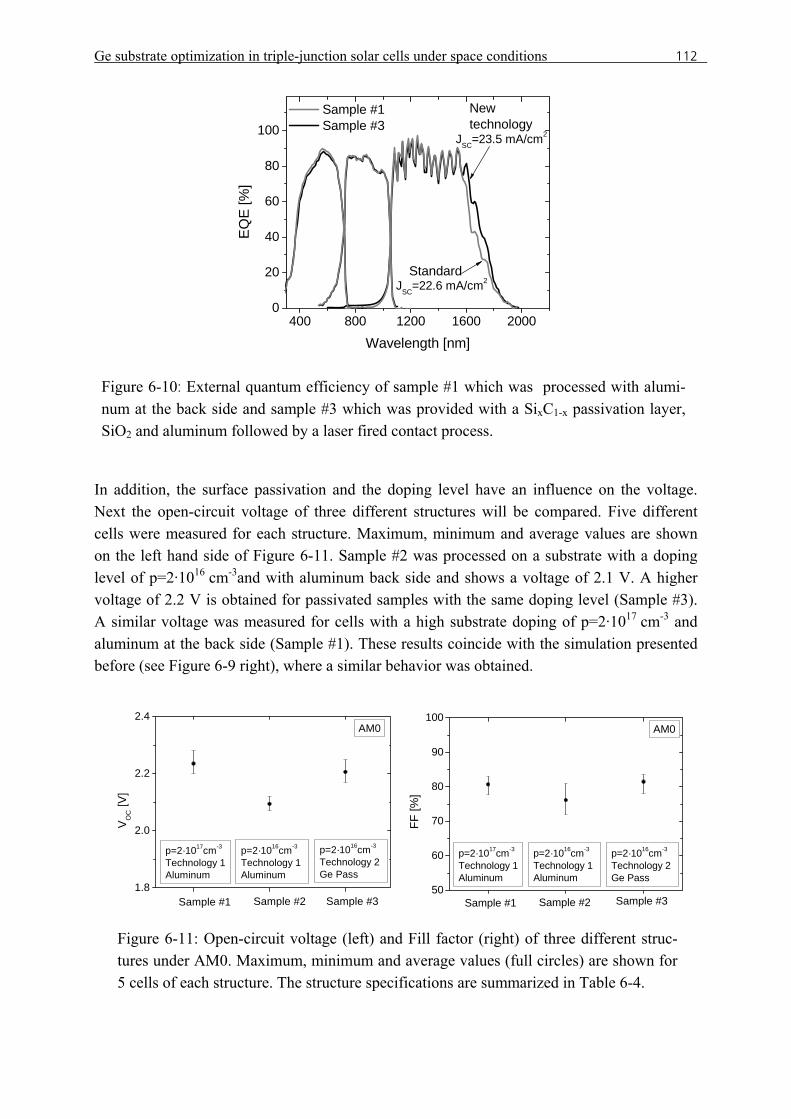
Ge substrate optimization in triple-junction solar cells under space conditions 112
400 800 1200 1600 20000
20
40
60
80
100
JSC=22.6 mA/cm2
Sample #1 Sample #3
EQ
E [%
]
Wavelength [nm]
New technology
JSC=23.5 mA/cm2
Standard
Figure 6-10: External quantum efficiency of sample #1 which was processed with alumi-num at the back side and sample #3 which was provided with a SixC1-x passivation layer, SiO2 and aluminum followed by a laser fired contact process.
In addition, the surface passivation and the doping level have an influence on the voltage. Next the open-circuit voltage of three different structures will be compared. Five different cells were measured for each structure. Maximum, minimum and average values are shown on the left hand side of Figure 6-11. Sample #2 was processed on a substrate with a doping level of p=2·1016 cm-3and with aluminum back side and shows a voltage of 2.1 V. A higher voltage of 2.2 V is obtained for passivated samples with the same doping level (Sample #3). A similar voltage was measured for cells with a high substrate doping of p=2·1017 cm-3 and aluminum at the back side (Sample #1). These results coincide with the simulation presented before (see Figure 6-9 right), where a similar behavior was obtained.
1.8
2.0
2.2
2.4
Sample #3
p=2·1016cm-3
Technology 2 Ge Pass
p=2·1016cm-3
Technology 1 Aluminum
VO
C [V
]
p=2·1017cm-3
Technology 1Aluminum
Sample #2Sample #1
AM0
50
60
70
80
90
100AM0
p=2·1016cm-3
Technology 2 Ge Pass
p=2·1016cm-3
Technology 1 Aluminum
p=2·1017cm-3
Technology 1Aluminum
Sample #3Sample #2
FF [%
]
Sample #1
Figure 6-11: Open-circuit voltage (left) and Fill factor (right) of three different struc-tures under AM0. Maximum, minimum and average values (full circles) are shown for 5 cells of each structure. The structure specifications are summarized in Table 6-4.
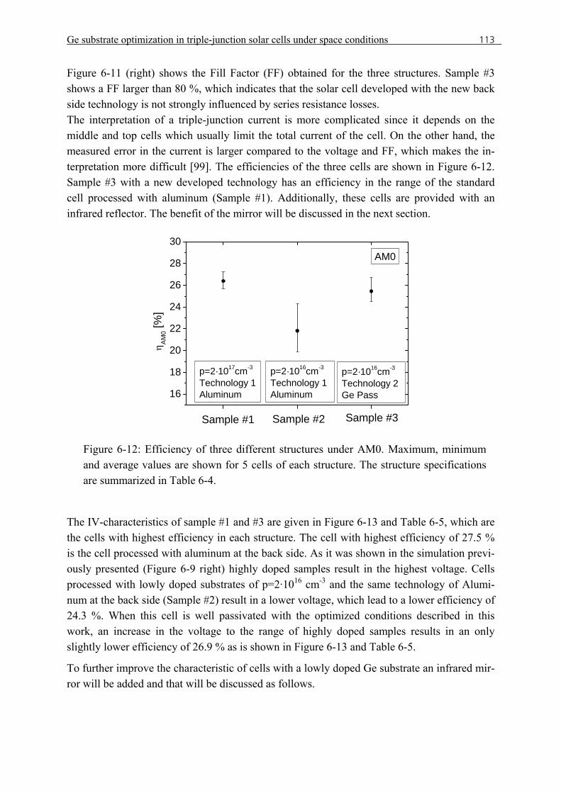
Ge substrate optimization in triple-junction solar cells under space conditions 113
Figure 6-11 (right) shows the Fill Factor (FF) obtained for the three structures. Sample #3 shows a FF larger than 80 %, which indicates that the solar cell developed with the new back side technology is not strongly influenced by series resistance losses. The interpretation of a triple-junction current is more complicated since it depends on the middle and top cells which usually limit the total current of the cell. On the other hand, the measured error in the current is larger compared to the voltage and FF, which makes the in-terpretation more difficult [99]. The efficiencies of the three cells are shown in Figure 6-12. Sample #3 with a new developed technology has an efficiency in the range of the standard cell processed with aluminum (Sample #1). Additionally, these cells are provided with an infrared reflector. The benefit of the mirror will be discussed in the next section.
16
18
20
22
24
26
28
30AM0
p=2·1017cm-3
Technology 1Aluminum
p=2·1016cm-3
Technology 1 Aluminum
p=2·1016cm-3
Technology 2 Ge Pass
η AM
0 [%
]
Sample #3Sample #2Sample #1
Figure 6-12: Efficiency of three different structures under AM0. Maximum, minimum and average values are shown for 5 cells of each structure. The structure specifications are summarized in Table 6-4.
The IV-characteristics of sample #1 and #3 are given in Figure 6-13 and Table 6-5, which are the cells with highest efficiency in each structure. The cell with highest efficiency of 27.5 % is the cell processed with aluminum at the back side. As it was shown in the simulation previ-ously presented (Figure 6-9 right) highly doped samples result in the highest voltage. Cells processed with lowly doped substrates of p=2·1016 cm-3 and the same technology of Alumi-num at the back side (Sample #2) result in a lower voltage, which lead to a lower efficiency of 24.3 %. When this cell is well passivated with the optimized conditions described in this work, an increase in the voltage to the range of highly doped samples results in an only slightly lower efficiency of 26.9 % as is shown in Figure 6-13 and Table 6-5.
To further improve the characteristic of cells with a lowly doped Ge substrate an infrared mir-ror will be added and that will be discussed as follows.
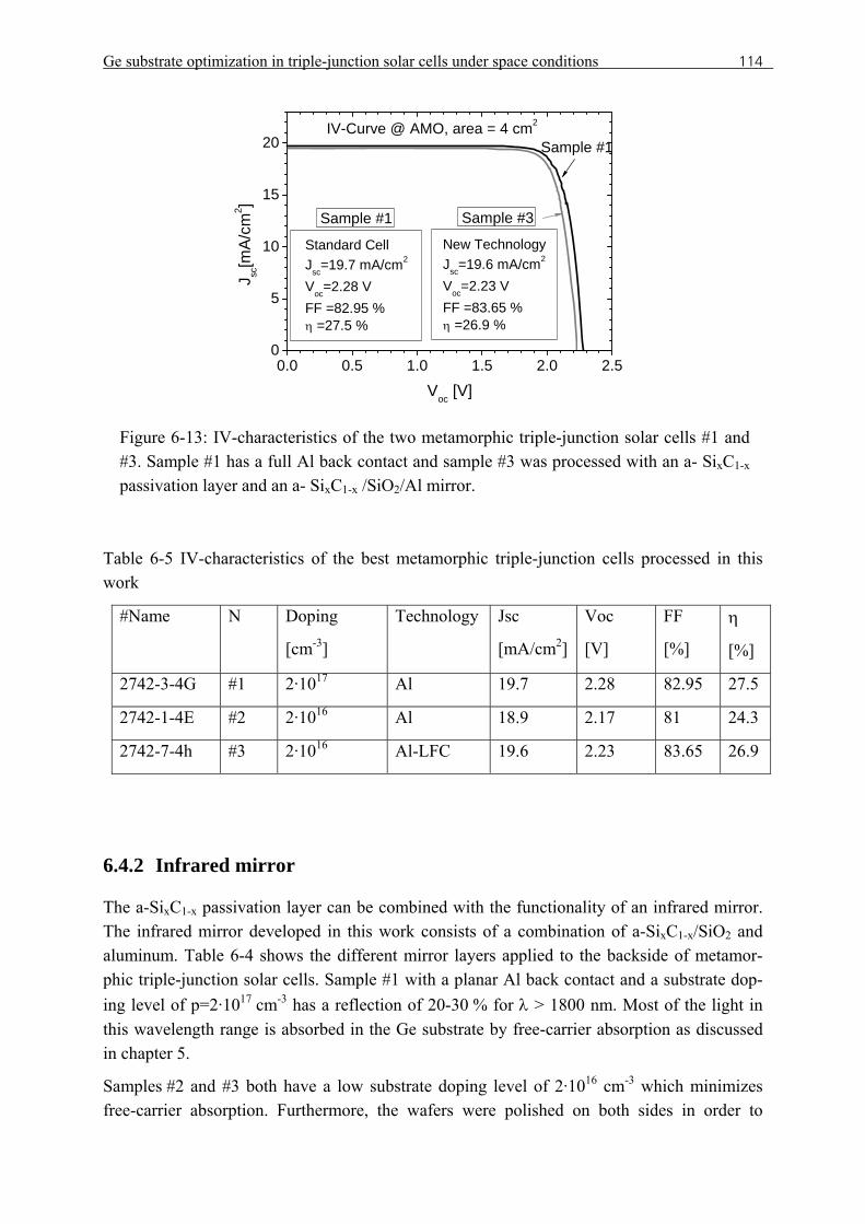
Ge substrate optimization in triple-junction solar cells under space conditions 114
0.0 0.5 1.0 1.5 2.0 2.50
5
10
15
20 Sample #1
Sample #3
New TechnologyJsc=19.6 mA/cm2
Voc=2.23 VFF =83.65 %η =26.9 %
Standard CellJsc=19.7 mA/cm2
Voc=2.28 VFF =82.95 %η =27.5 %
IV-Curve @ AMO, area = 4 cm2
J sc[m
A/c
m2 ]
Voc [V]
Sample #1
Figure 6-13: IV-characteristics of the two metamorphic triple-junction solar cells #1 and #3. Sample #1 has a full Al back contact and sample #3 was processed with an a- SixC1-x passivation layer and an a- SixC1-x /SiO2/Al mirror.
Table 6-5 IV-characteristics of the best metamorphic triple-junction cells processed in this work
#Name N Doping
[cm-3]
Technology Jsc
[mA/cm2]
Voc
[V]
FF
[%]
η
[%]
2742-3-4G #1 2·1017 Al 19.7 2.28 82.95 27.5
2742-1-4E #2 2·1016 Al 18.9 2.17 81 24.3
2742-7-4h #3 2·1016 Al-LFC 19.6 2.23 83.65 26.9
6.4.2 Infrared mirror
The a-SixC1-x passivation layer can be combined with the functionality of an infrared mirror. The infrared mirror developed in this work consists of a combination of a-SixC1-x/SiO2 and aluminum. Table 6-4 shows the different mirror layers applied to the backside of metamor-phic triple-junction solar cells. Sample #1 with a planar Al back contact and a substrate dop-ing level of p=2·1017 cm-3 has a reflection of 20-30 % for λ > 1800 nm. Most of the light in this wavelength range is absorbed in the Ge substrate by free-carrier absorption as discussed in chapter 5.
Samples #2 and #3 both have a low substrate doping level of 2·1016 cm-3 which minimizes free-carrier absorption. Furthermore, the wafers were polished on both sides in order to
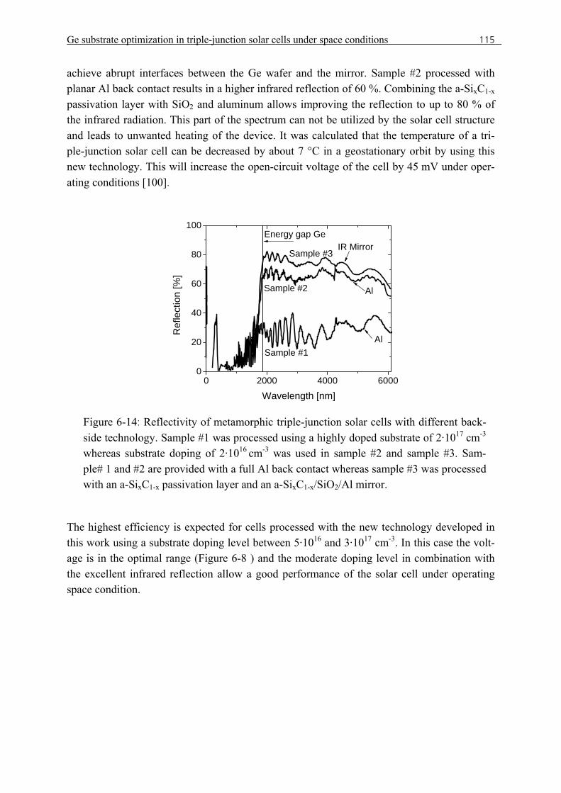
Ge substrate optimization in triple-junction solar cells under space conditions 115
achieve abrupt interfaces between the Ge wafer and the mirror. Sample #2 processed with planar Al back contact results in a higher infrared reflection of 60 %. Combining the a-SixC1-x passivation layer with SiO2 and aluminum allows improving the reflection to up to 80 % of the infrared radiation. This part of the spectrum can not be utilized by the solar cell structure and leads to unwanted heating of the device. It was calculated that the temperature of a tri-ple-junction solar cell can be decreased by about 7 °C in a geostationary orbit by using this new technology. This will increase the open-circuit voltage of the cell by 45 mV under oper-ating conditions [100].
0 2000 4000 60000
20
40
60
80
100
Sample #1
Sample #2 Al
IR Mirror
Ref
lect
ion
[%]
Wavelength [nm]
Energy gap Ge
Al
Sample #3
Figure 6-14: Reflectivity of metamorphic triple-junction solar cells with different back-side technology. Sample #1 was processed using a highly doped substrate of 2·1017 cm-3
whereas substrate doping of 2·1016 cm-3 was used in sample #2 and sample #3. Sam-ple# 1 and #2 are provided with a full Al back contact whereas sample #3 was processed with an a-SixC1-x passivation layer and an a-SixC1-x/SiO2/Al mirror.
The highest efficiency is expected for cells processed with the new technology developed in this work using a substrate doping level between 5·1016 and 3·1017 cm-3. In this case the volt-age is in the optimal range (Figure 6-8 ) and the moderate doping level in combination with the excellent infrared reflection allow a good performance of the solar cell under operating space condition.

Ge substrate optimization in triple-junction solar cells under space conditions 116
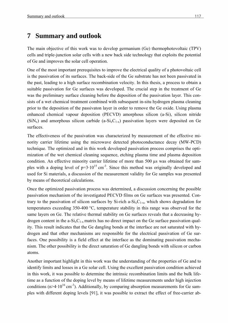
Summary and outlook 117
7 Summary and outlook
The main objective of this work was to develop germanium (Ge) thermophotovoltaic (TPV) cells and triple-junction solar cells with a new back side technology that exploits the potential of Ge and improves the solar cell operation.
One of the most important prerequisites to improve the electrical quality of a photovoltaic cell is the passivation of its surfaces. The back-side of the Ge substrate has not been passivated in the past, leading to a high surface recombination velocity. In this thesis, a process to obtain a suitable passivation for Ge surfaces was developed. The crucial step in the treatment of Ge was the preliminary surface cleaning before the deposition of the passivation layer. This con-sists of a wet chemical treatment combined with subsequent in-situ hydrogen plasma cleaning prior to the deposition of the passivaton layer in order to remove the Ge oxide. Using plasma enhanced chemical vapour deposition (PECVD) amorphous silicon (a-Si), silicon nitride (SiNx) and amorphous silicon carbide (a-SixC1-x) passivation layers were deposited on Ge surfaces.
The effectiveness of the passivation was characterized by measurement of the effective mi-nority carrier lifetime using the microwave detected photoconductance decay (MW-PCD) technique. The optimized and in this work developed passivation process comprises the opti-mization of the wet chemical cleaning sequence, etching plasma time and plasma deposition condition. An effective minority carrier lifetime of more than 500 µs was obtained for sam-ples with a doping level of p=3·1015 cm-3. Since this method was originally developed and used for Si materials, a discussion of the measurement validity for Ge samples was presented by means of theoretical calculations.
Once the optimized passivation process was determined, a discussion concerning the possible passivation mechanism of the investigated PECVD films on Ge surfaces was presented. Con-trary to the passivation of silicon surfaces by Si-rich a-SixC1-x, which shows degradation for temperatures exceeding 350-400 °C, temperature stability in this range was observed for the same layers on Ge. The relative thermal stability on Ge surfaces reveals that a decreasing hy-drogen content in the a-SixC1-x matrix has no direct impact on the Ge surface passivation qual-ity. This result indicates that the Ge dangling bonds at the interface are not saturated with hy-drogen and that other mechanisms are responsible for the electrical passivation of Ge sur-faces. One possibility is a field effect at the interface as the dominating passivation mecha-nism. The other possibility is the direct saturation of Ge dangling bonds with silicon or carbon atoms.
Another important highlight in this work was the understanding of the properties of Ge and to identify limits and losses in a Ge solar cell. Using the excellent passivation condition achieved in this work, it was possible to determine the intrinsic recombination limits and the bulk life-time as a function of the doping level by means of lifetime measurements under high injection conditions (n>4·1016 cm-3). Additionally, by comparing absorption measurements for Ge sam-ples with different doping levels [91], it was possible to extract the effect of free-carrier ab-
Summary and outlook 118
sorption (FCA) in p-Ge. The better understanding of Ge due to the determination of these properties led to the identification of the optimal parameters for the processing of the TPV and triple-junction solar cells.
To obtain a suitable technology for Ge solar cells a new process for the rear side of the cells was developed. This technology incorporates an optimized passivation layer (a-SixC1-x or a-Si). At the same time, the passivation layer was used as a part of a multi layer back surface infrared reflector which consists of SiO2 and aluminum layers. The cells were contacted on the rear side by means of either a photolithographic step or by laser fired contacts (LFC).
This new structure increases the cells’ spectral response in the long wavelength range between 1.6 and 2 µm when the diffusion length is comparable or larger than the thickness of the base layer. TPV cells with a doping level around p=1016 cm-3 show an increase of 10 % in the volt-age under AM1.5g spectrum when using this structure due to the low surface recombination velocity at the back side. An external reflection between 70 % and 80 % was achieved for wavelengths below the band gap of Ge, allowing the recycling of these photons by reflecting them back to the TPV emitter which leads to a total system efficiency enhancement.
For the conversion into electricity of radiation with a micro-structured tungsten emitter spec-trum at 1373 K with an incident intensity of 2.5 W/cm2 an efficiency of 16 % was calculated using a TPV cell with a highly doped Ge substrate (2·1017 cm-3). By means of PC1D simula-tion it was shown that the full potential of this technology for TPV cells is expected to show up when using a substrate doping level of p=4·1016 cm-3 and a wafer thickness between 250 µm and 500 µm.
In order to explore the potential of Ge bottom cells in multi-junction space solar cells, simula-tions applying the software PC1D have been carried out. The optimum Ge substrate thickness for processing the cells was 250 µm and the optimum substrate doping lies between 5·1016 and 3·1017cm-3. A back surface recombination velocity below 100 cm/s and an infrared reflec-tion higher than 60 % was necessary to obtain the highest efficiency using the new back side technology. Using these Ge specifications, the developed back side technology exploits the potential of Ge as an active part of the cell, reduces the operating temperature and improves the solar cell efficiency.
Triple-junction solar cells with the newly developed back side technology were processed. The standard technology uses a substrate doping level of p=2·1017 cm-3, whereas the new cells are processed with a Ge substrate with a doping level of p=2·1016 cm-3. An increase of 5 % in short-circuit photocurrent of the Ge subcell was obtained for the cells processed with the new cell technology. Additionally, the infrared mirror and the low substrate doping level allow to reflect up to 80 % of the infrared radiation of wavelengths above the band gap of Ge (λ>1850 nm). This part of the spectrum cannot be used by the solar cell structure and leads to an unwanted heating of the device. It has been shown that the temperature of a triple-junction solar cell can be decreased by about 7 K in a geostationary satellite by using the newly devel-oped back surface mirror. This will increase the open–circuit voltage of the cell by 45 mV under operating condition. An experimentally realized AM0 efficiency of 26.9 % was ob-tained for triple-junction space solar cells using this optimized technology.
Summary and outlook 119
Future research in Ge material and Ge solar cell technology should focus on the following topics:
1) Cell characteristics under real cell operation conditions.
The simulation results presented in this thesis show the optimal Ge substrate doping level to process TPV cells. The next step to follow should be the optimization of the pitch of the back side contact for the optimal doping level at TPV conditions. Furthermore, as pointed out in the text a set up which allows the measurement for lowly doped Ge substrates under high light concentration is necessary. Finally, stability of the passivation layer should be analyzed under real TPV condition.
Solar cells performance is reduced in space conditions by several factors. The major factor is solar cell degradation due to charged particle environment at near and outer space (radiation of electrons and protons). The radiation hardness of Ge solar cells with the specifications and technologies described is this work was recently investigated by [101, 102]. After electron irradiation, additional SRH recombination centers lead to a decrease in minority carrier diffu-sion lengths which lead to a decrease of EQE in the wavelength range between 1550 nm and 2000 nm. The effect of the radiation on the Ge bulk lifetime and on the passivation layer qual-ity is still not clear and should be further examined.
2) Passivation in Ge
The passivation mechanism in Ge is not well understood until the moment. Recent work show that the passivation mechanism in Ge may be related to silicon or/and carbon dangling bonds. This topic will be futher discussed in [103] by means of surface photovoltage (SPV), trans-mission electron microscopy (TEM) and Fourier-Transform-Infrarot spectrometer (FTIR) measurements.
Alternatives for a-Si or a-SiC passivation layers like Aluminum oxide (Al2O3) could be con-sidered to passivate p-Ge. In p-Si Al2O3 has been proved to be an excellent and thermally sta-ble passivation layer due to its negative fixed charge density [104]. In Ge similar effects are not necessarily expected since passivation mechanisms in p-Ge is very different to silicon. More passivation experiments shoud be done in the future with different passivation layers to clarify the dominant passivation mechanism in Ge and to find out more information about the Ge surface properties.
3) Ge material constant
In this work a first estimation was carried out for the free-carrier absorption coefficients in p-Ge. As discussed in the text more measurements are necessary to achieve more accuracy and solidity in the measured values.
The determination of Ge recombination parameters, Ca and B, is a very complex topic since it requires lifetime measurements under high injection conditions. Unfourtunately microwave detected photoconductance decay technique (MW-PCD) is not a suitable method for these conditions [105]. Other measurement set-ups like Photoluminescence (PL) or Quasi Steady State Photoconductivity (QSSPC) could result in a simpler and more accurate method to measure effective lifetime at high injection conditions to determine Ca and B coefficients.

Summary and outlook 120
Deutsche Zusammenfassung 121
8 Deutsche Zusammenfassung
In der vorliegenden Doktorarbeit wurde eine neue Rückseitentechnologie für Germanium (Ge) thermophotovoltaische (TPV) Solarzellen und hoch effiziente Dreifachsolarzellen für Weltraumanwendungen entwickelt. Das Ziel dieser neuen Struktur ist es, das Potential von Ge im Sinne der photovoltaischen Energiewandlung voll auszunutzen und das Leistungsverhalten der Zellen zu verbessern.
Eine der wichtigsten Voraussetzungen, um die elektrischen Eigenschaften einer Solarzelle zu verbessern, ist es, eine geeignete Oberflächenpassivierung zu erzielen. Die Rückseite einer Photovoltaikzelle ist in der Regel nicht passiviert, was zu einer hohen Oberflächen-rekombinationsgeschwindigkeit führt. Im Rahmen der vorliegenden Arbeit wurde ein techno-logischer Prozess entwickelt, um eine geeignete Oberflächenpassivierung für Ge zu erreichen. Der entscheidende Schritt in der Behandlung der Proben war die geeignete Vorreinigung vor dem darauffolgenden Abscheiden der Passivierungsschicht. Diese Vorreinigung setzt sich aus einer nasschemischen Behandlung, kombiniert mit einer anschließenden in-situ Wasserstoff-Plasmareinigung zusammen, um das am Ge anhaftende native Oxid vor der Passivierungsab-scheidung zu entfernen. PECVD Plasmatechnologie wurde benutzt, um amorphes Silicium (a-Si), Silicium-Nitrid (SiNx) und amorphes Silicium-Carbid (a-SixC1-x) abzuscheiden.
Die Effektivität der Passivierung wurde mit Hilfe von Mikrowellen-PCD Messungen der Mi-noritätsladungsträgerlebensdauer charakterisiert. Der in dieser Arbeit entwickelte und opti-mierte Passivierungsprozess besteht aus einer Optimierung der Reihenfolge der nasschemi-schen Reinigung, der Plasmaätzzeit und der Plasma Abscheidungsbedingungen. Eine effekti-ve Minoritätsladungsträgerlebensdauer von mehr als 500 µs für Proben mit einer Dotierung von p=3·1015 cm-3 wurde gemessen. Da die hier angewandte Lebensdauermessmethode ur-sprünglich für Silizium entwickelt worden ist, wurde im Rahmen dieser Arbeit eine Diskussi-on über die Anwendbarkeit dieser Messmethode für Ge Proben mit Hilfe theoretischen Rech-nungen dargelegt.
Nachdem der optimierte Passivierungsprozess bestimmt war, wurde im Rahmen der Disserta-tion eine theoretische Betrachtung möglicher Passivierungsmechanismen auf Ge-Oberflächen vorgestellt. Im Gegensatz zu Si-Oberflächen, die eine Degradation für Temperaturen ab 300-400 °C zeigen, wurde eine Temperaturstabilität in diesem Bereich für SixC1-x und SiNx Schichten auf Ge Oberflächen festgestellt. Die thermische Stabilität auf Ge Oberflächen zeigt, dass ein abnehmender Wasserstoffgehalt in der SixC1-x Matrix keinen direkten Einfluss auf die Oberflächenpassivierungsqualität von Ge hat. Diese Ergebnisse zeigen, dass andere Effekte verantwortlich für die Passivierung von Ge-Oberflächen sein müssen. Eine Möglichkeit ist ein Feldeffekt oder eine Sättigung der Ge dangling-bonds mit Kohlenstoff oder Silicium Atomen.
Ein weiteres wichtiges Thema dieser Arbeit war es, die Eigenschaften von Ge besser zu ver-stehen und somit die Limitierungen und Verluste in einer Ge-Zelle zu bestimmen. Unter An-wendung der in dieser Arbeit entwickelten und optimierten Passivierungsmethode konnte die intrinsische Minoritätsladungsträgerrekombination in p-Ge mittels Lebensdauermessungen
Deutsche Zusammenfassung 122
unter Hochinjektionsbedingungen (Δn>4x1016 cm-3) bestimmt werden. Eine Parametrisierung für die Minoritätsladungsträgerlebensdauer im Volumenmaterial in Abhängigkeit der Dotie-rung konnte so ebenfalls bestimmt werden. Zusätzlich wurde der Effekt der Freien-Ladungsträger-Absorption (FCA) bestimmt, mittels eines Vergleichs der Absorptionskoeffi-zienten von niedrig- und hochdotierten Proben [91]. Das verbesserte Verständnis von Ge durch die Bestimmung dieser Eigenschaften führte zur Identifizierung der optimalen Parame-ter für die Prozessierung der TPV und Mehrfach-Solarzellen.
Um eine geeignete Solarzellentechnologie zu erzielen, wurde eine neue Rückseitentechnolo-gie entwickelt. Sie besteht aus optimierten Passivierungsschichten aus SixC1-x oder a-Si. Gleichzeitig wurde die Passivierungsschicht als Teil eines Mehrschichtstapels zum Aufbau eines Infrarotspiegels benutzt, der aus SiO2 und Aluminium besteht. Die Zellen wurden auf der Rückseite mittels Photolitographie oder mittels sog. Laser Fired Contacts (LFC) kontak-tiert. Unter Anwendung dieser neu entwickelten Strukturen zeigt sich ein Anstieg der externen Quanteneffizienz (EQE) der Zellen für Wellenlängen in Bereich (1.6 µm<λ< 2µm), wenn die Diffusionslänge vergleichbar oder größer als die Schichtdicke des Ge Substrates ist. TPV-Zellen mit einer Dotierung von etwa p = 1016 cm-3 zeigen unter Verwendung dieser neu entwickelten Strukturen eine Erhöhung um 10 % in der Spannung unter Verwendung eines AM1.5g Spektrums. Die Ursache dafür liegt in den niedrigen Oberflächenrekombinations-geschwindigkeit and der neuen Rückseite. Für Wellenlängen oberhalb der Bandlückenenergie von Ge (λ > 1850 nm) wurde eine externe Reflexion von 70 bis 80 % erreicht, was ein Recyc-ling dieser Photonen im TPV-Emitter erlaubt und zu einer Gesamtsystemwirkungsgraderhö-hung führt. Die so weiterentwickelte Solarzellentechnologie führte zu einem Wirkungsgrad von 16 % unter Annahme eines mikrostrukturierten Wolframemitters mit einer Temperatur von 1373 K, einer Intensität von 2.5 W/cm2 und einer Substratdotierung von p = 2·1017 cm-3. Es wurde mittels PC1D-Simulationen gezeigt, dass das volle Potential dieser Technologie für TPV Zellen unter Verwendung einer Substratdotierung von p = 4·1016 cm-3 und einer Wafer-dicke zwischen 250 µm und 500 µm erwartet werden kann. Um das Potential von Ge als Unterzelle in einer Dreifachsolarzelle zu untersuchen, wurden ebenfalls Simulationen mit dem Programm PC1D durchgeführt. Die optimale Substratdicke für Ge ergab sich zu 250 µm, als optimale Substratdotierung ergab sich ein Bereich zwischen 5·1016 cm-3 und 3·1017 cm-3. Eine Rückseitenoberflächenrekombinationsgeschwindigkeit klei-ner als 100 cm/s und eine Infrarotreflexion von über 60 % sind nötig, um höchste Solarzel-lenwirkungsgrade mit der neu entwickelten Solarzellentechnologie zu erreichen. Unter Ver-wendung von Ge Substraten, die diese Spezifikationen erfüllen, würde das Potential von Ge völlig ausgenutzt. Außerdem verringert sich die Temperatur der Zelle im Betrieb, wodurch der Solarzellenwirkungsgrad erhöht wird. Dreifachsolarzellen mit der neu entwickelten Rückseitentechnologie wurden prozessiert. Die Standardtechnologie benutzt eine Substratdotierung von p =2·1017 cm-3, wohingegen Substra-te mit einer Dotierung von p =2·10 16 cm-3 für die neu entwickelte Solarzellentechnologie be-nutzt wurden. Für die Dreifachzellen, die mit der neuen Technologie prozessiert wurden, konnte eine Erhöhung von 5 % im Kurzschluß-Photostrom der Ge-Teilzelle erreicht werden.
Deutsche Zusammenfassung 123
Der Infrarotspiegel und die niedrige Substratdotierung führen zusätzlich zu einer Erhöhung der Reflexion auf bis zu 80 % für Wellenlängen oberhalb der Bandlücke von Ge (λ > 1850 nm). Dieser Teil des Spektrums kann nicht zur Stromgeneration in einer Ge-Zelle genutzt werden und führt zu einer unerwünschten Erwärmung der Solarzelle. Es konnte ge-zeigt werden, dass sich für Dreifachsolarzellen mit der neu entwickelten Solarzellentechnolo-gie, bei Annahme eines geostationären Orbits, eine um 7 K niedrigere Solarzellentemperatur im Betrieb ergeben kann – im Vergleich zu Dreifachsolarzellen mit Standardtechnologie, wie sie derzeit für Weltraumsolarzellen eingesetzt wird. Die weniger ausgeprägte Erwärmung der Solarzellen entspricht einer um etwa 45 mV höheren offenen Klemmen Spannung der Solar-zellen. Ein experimentell realizierte AM0 Wirkungsgrad von 26.9 % konnte unter Verwen-dung der neuen Solarzellentechnologie erreicht werden.
Die zukünftige Forschung im Bereich der Ge-Material und Ge-Solarzellentechnologie sollte sich auf folgende Themen konzentrieren: 1) Solarzellen Charakteristika unter realen Einsatzbedingungen In diese Arbeit wurde die optimale Dotierungkonzentration von Ge TPV Zellen mittels rech-nergestützter Simulationen bestimmt. Der nächste Schritt sieht die Optimierung des Abstands der Punktkontakte auf die Rückseite vor. Außerdem sollten IV-Messungen für die niedrig dotierten Ge Substrate unter hohen Lichtkonzentrationen möglich sein. Desweiteren ist die Analyse zur Stabilität der Passivierungsschicht unter realem TPV Zustand von hohem Interes-se. Die Leistung von Solarzellen im Weltraum ist durch mehrere Faktoren reduziert. Die haupt-sächliche Solarzellendegradation resultiert aus dem Beschuss durch kosmische hochenergeti-sche Elektronen und Protonen. Die Strahlungsresistenz der Ge-Solarzellen, deren Spezifikati-onen und Technologien in dieser Arbeit beschrieben sind, wurde kürzlich von [101, 102] un-tersucht. Nach der Elektronenbestrahlung führen zusätzliche SRH-Rekombinationszentren zu einer Reduzierung der Minoritätsladungsträgerdiffusionslänge was eine Reduzierung der EQE im Bereich zwischen 1550 nm und 2000 nm bewirkt. Der Einfluss der Strahlung auf die Ge Bulk-Lebensdauer und auf die Qualität der Passivierungsschicht ist noch nicht vollständig verstanden und sollte weiter untersucht werden. 2) Passivierung in Ge Der Passivierungsmechanismus in Ge ist bisher nicht gut verstanden. Neuere Arbeiten zeigen, dass die Passivierungmechanismen in Ge ggf. auf Silizium oder Kohlenstoff „dangling-bonds“ zurückgeführt werden können. Dieses Thema wird gegenwärtig mittels [103] Oberflä-chenphotospannungsmethode (SPV), Transmissionselektronenmikroskopie (TEM) und Fou-rier-Transform-Infrarotspektrometer (FTIR) Messungen weiter untersucht. Alternativen zu amorphem Silicium und amorphem Silicium Karbid wie Aluminiumoxid (Al2O3) könnten als p-Ge Passivierung benutzt werden. In p-Si Al2O3 ist erwiesen, dass dies eine hervorragende und thermisch stabile Passivierungsschicht aufgrund seiner festen negati-ve Ladungsdichte ausbildet [104]. In Ge sind ähnliche Effekte nicht notwendigerweise zu erwarten, da Passivierungsmechanismen in p-Ge sehr unterschiedlich von p-Si sind. Weitere
Deutsche Zusammenfassung 124
Passivierungsexperimente sollten in der Zukunft mit verschiedenen Passivierungsschichten getan werden, um den dominierenden Passivierungmechanismus in Ge zu klären und um mehr Informationen über die Ge Oberflächeneigenschaften herauszufinden.
3) Ge Material Konstanten
In dieser Arbeit wird eine erste Bestimmung für die Freie-Ladungsträger- Absorptionskoeffi-zienten (FCA) in p-Ge durchgeführt. Wie im Text diskutiert wurde, sind noch mehrere Mes-sungen notwendig um die geforderte Genauigkeit und Eindeutigkeit der gesuchten Material-parameter zu erreichen. Die Bestimmung des Ge-Rekombinationsparameter Ca und B, ist ein sehr komplexes Thema, da für die Bestimmung Minoritätsladungsträgerslebensdauer Messungen unter hohen Uber-schussladungsträgerkonzentration erfordlich sind. Leider ist die hierfür bisher eingesetzte (MW-PCD)-Technik keine geeignete Methode für diese Bedingungen [105]. Andere Messun-gen wie Photoluminescence (PL) oder Quasi Steady State Photoleitung (QSSPC) könnten eine einfachere und genauere Methode sein, um die effektive Lebensdauer bei hohen Injektionsbe-dienung zu messen und die Ca-und B-Koeffizienten zu ermitteln.
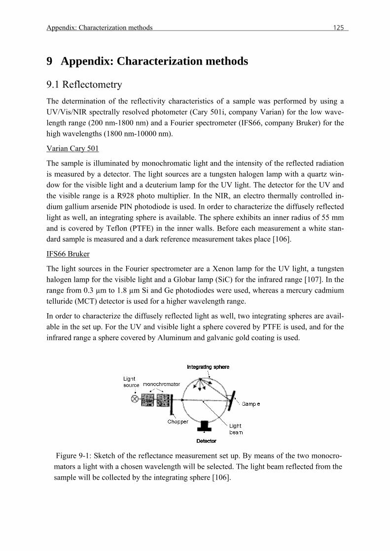
Appendix: Characterization methods 125
9 Appendix: Characterization methods
9.1 Reflectometry The determination of the reflectivity characteristics of a sample was performed by using a UV/Vis/NIR spectrally resolved photometer (Cary 501i, company Varian) for the low wave-length range (200 nm-1800 nm) and a Fourier spectrometer (IFS66, company Bruker) for the high wavelengths (1800 nm-10000 nm).
Varian Cary 501
The sample is illuminated by monochromatic light and the intensity of the reflected radiation is measured by a detector. The light sources are a tungsten halogen lamp with a quartz win-dow for the visible light and a deuterium lamp for the UV light. The detector for the UV and the visible range is a R928 photo multiplier. In the NIR, an electro thermally controlled in-dium gallium arsenide PIN photodiode is used. In order to characterize the diffusely reflected light as well, an integrating sphere is available. The sphere exhibits an inner radius of 55 mm and is covered by Teflon (PTFE) in the inner walls. Before each measurement a white stan-dard sample is measured and a dark reference measurement takes place [106].
IFS66 Bruker
The light sources in the Fourier spectrometer are a Xenon lamp for the UV light, a tungsten halogen lamp for the visible light and a Globar lamp (SiC) for the infrared range [107]. In the range from 0.3 µm to 1.8 µm Si and Ge photodiodes were used, whereas a mercury cadmium telluride (MCT) detector is used for a higher wavelength range.
In order to characterize the diffusely reflected light as well, two integrating spheres are avail-able in the set up. For the UV and visible light a sphere covered by PTFE is used, and for the infrared range a sphere covered by Aluminum and galvanic gold coating is used.
Figure 9-1: Sketch of the reflectance measurement set up. By means of the two monocro-mators a light with a chosen wavelength will be selected. The light beam reflected from the sample will be collected by the integrating sphere [106].
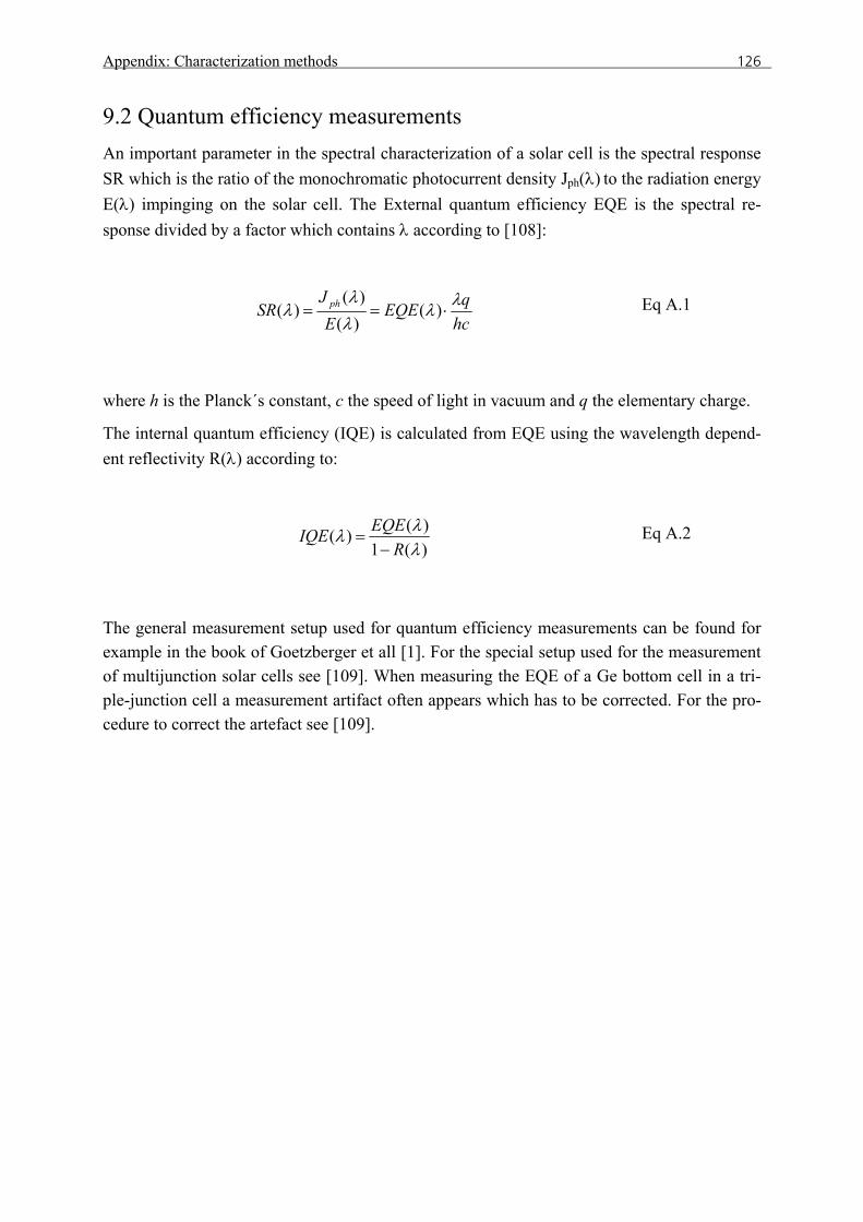
Appendix: Characterization methods 126
9.2 Quantum efficiency measurements An important parameter in the spectral characterization of a solar cell is the spectral response SR which is the ratio of the monochromatic photocurrent density Jph(λ) to the radiation energy E(λ) impinging on the solar cell. The External quantum efficiency EQE is the spectral re-sponse divided by a factor which contains λ according to [108]:
hcqEQE
EJ
SR ph λλλλ
λ ⋅== )()()(
)( Eq A.1
where h is the Planck´s constant, c the speed of light in vacuum and q the elementary charge.
The internal quantum efficiency (IQE) is calculated from EQE using the wavelength depend-ent reflectivity R(λ) according to:
)(1)()(
λλλ
REQEIQE
−= Eq A.2
The general measurement setup used for quantum efficiency measurements can be found for example in the book of Goetzberger et all [1]. For the special setup used for the measurement of multijunction solar cells see [109]. When measuring the EQE of a Ge bottom cell in a tri-ple-junction cell a measurement artifact often appears which has to be corrected. For the pro-cedure to correct the artefact see [109].
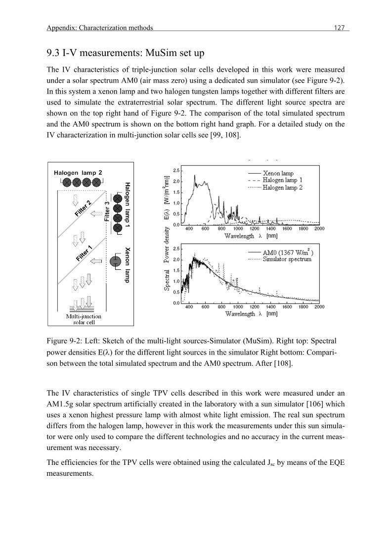
Appendix: Characterization methods 127
9.3 I-V measurements: MuSim set up The IV characteristics of triple-junction solar cells developed in this work were measured under a solar spectrum AM0 (air mass zero) using a dedicated sun simulator (see Figure 9-2). In this system a xenon lamp and two halogen tungsten lamps together with different filters are used to simulate the extraterrestrial solar spectrum. The different light source spectra are shown on the top right hand of Figure 9-2. The comparison of the total simulated spectrum and the AM0 spectrum is shown on the bottom right hand graph. For a detailed study on the IV characterization in multi-junction solar cells see [99, 108].
Figure 9-2: Left: Sketch of the multi-light sources-Simulator (MuSim). Right top: Spectral power densities E(λ) for the different light sources in the simulator Right bottom: Compari-son between the total simulated spectrum and the AM0 spectrum. After [108].
The IV characteristics of single TPV cells described in this work were measured under an AM1.5g solar spectrum artificially created in the laboratory with a sun simulator [106] which uses a xenon highest pressure lamp with almost white light emission. The real sun spectrum differs from the halogen lamp, however in this work the measurements under this sun simula-tor were only used to compare the different technologies and no accuracy in the current meas-urement was necessary.
The efficiencies for the TPV cells were obtained using the calculated Jsc by means of the EQE measurements.

Appendix: Characterization methods 128
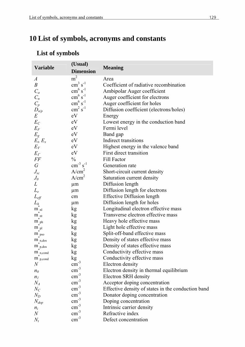
List of symbols, acronyms and constants 129
10 List of symbols, acronyms and constants
List of symbols
Variable (Usual) Dimension
Meaning
A m2 Area B cm3 s-1 Coefficient of radiative recombination Ca cm6 s-1 Ambipolar Auger coefficient Cn cm6 s-1 Auger coefficient for electrons Cp cm6 s-1 Auger coefficient for holes Dn/p cm2 s-1 Diffusion coefficient (electrons/holes) E eV Energy EC eV Lowest energy in the conduction band EF eV Fermi level Eg eV Band gap Et, Ex eV Indirect transitions EV eV Highest energy in the valence band EΓ eV First direct transition FF % Fill Factor G cm-3 s-1 Generation rate Jsc A/cm2 Short-circuit current density J0 A/cm2 Saturation current density L µm Diffusion length Le µm Diffusion length for electrons Leff cm Effective Diffusion length Lh µm Diffusion length for holes m*
nl kg Longitudinal electron effective mass m*
nt kg Transverse electron effective mass m*
ph kg Heavy hole effective mass m*
pl kg Light hole effective mass m*
pso kg Split-off-band effective mass m*
n,dos kg Density of states effective mass m*
p,dos kg Density of states effective mass m*
n,cond kg Conductivity effective mass m*
p,cond kg Conductivity effective mass N cm-3 Electron density n0 cm-3 Electron density in thermal equilibrium n1 cm-3 Electron SRH density NA cm-3 Acceptor doping concentration NC cm-3 Effective density of states in the conduction band ND cm-3 Donator doping concentration Ndop cm-3 Doping concentration ni cm-3 Intrinsic carrier density N cm-3 Refractive index Nt cm-3 Defect concentration
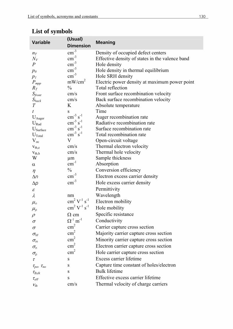
List of symbols, acronyms and constants 130
List of symbols
Variable (Usual) Dimension
Meaning
nT cm-3 Density of occupied defect centers NV cm-3 Effective density of states in the valence band P cm-3 Hole density p0 cm-3 Hole density in thermal equilibrium p1 cm-3 Hole SRH density Pmpp mW/cm2 Electric power density at maximum power point RT % Total reflection Sfront cm/s Front surface recombination velocity Sback cm/s Back surface recombination velocity T K Absolute temperature t s Time UAuger cm-3 s-1 Auger recombination rate URad cm-3 s-1 Radiative recombination rate USurface cm-3 s-1 Surface recombination rate UTotal cm-3 s-1 Total recombination rate Voc V Open-circuit voltage vth,e cm/s Thermal electron velocity vth,h cm/s Thermal hole velocity W µm Sample thickness α cm-1 Absorption η % Conversion efficiency Δn cm-3 Electron excess carrier density Δp cm-3 Hole excess carrier density ε Permittivity λ nm Wavelength μn cm2 V-1 s-1 Electron mobility μp cm2 V-1 s-1 Hole mobility ρ Ω cm Specific resistance σ Ω-1 m-1 Conductivity σ cm2 Carrier capture cross section σM cm2 Majority carrier capture cross section σm cm2 Minority carrier capture cross section σn cm2 Electron carrier capture cross section σp cm2 Hole carrier capture cross section τ s Excess carrier lifetime τpo, τno s Capture time constant of holes/electron τBulk s Bulk lifetime τeff s Effective excess carrier lifetime νth cm/s Thermal velocity of charge carriers
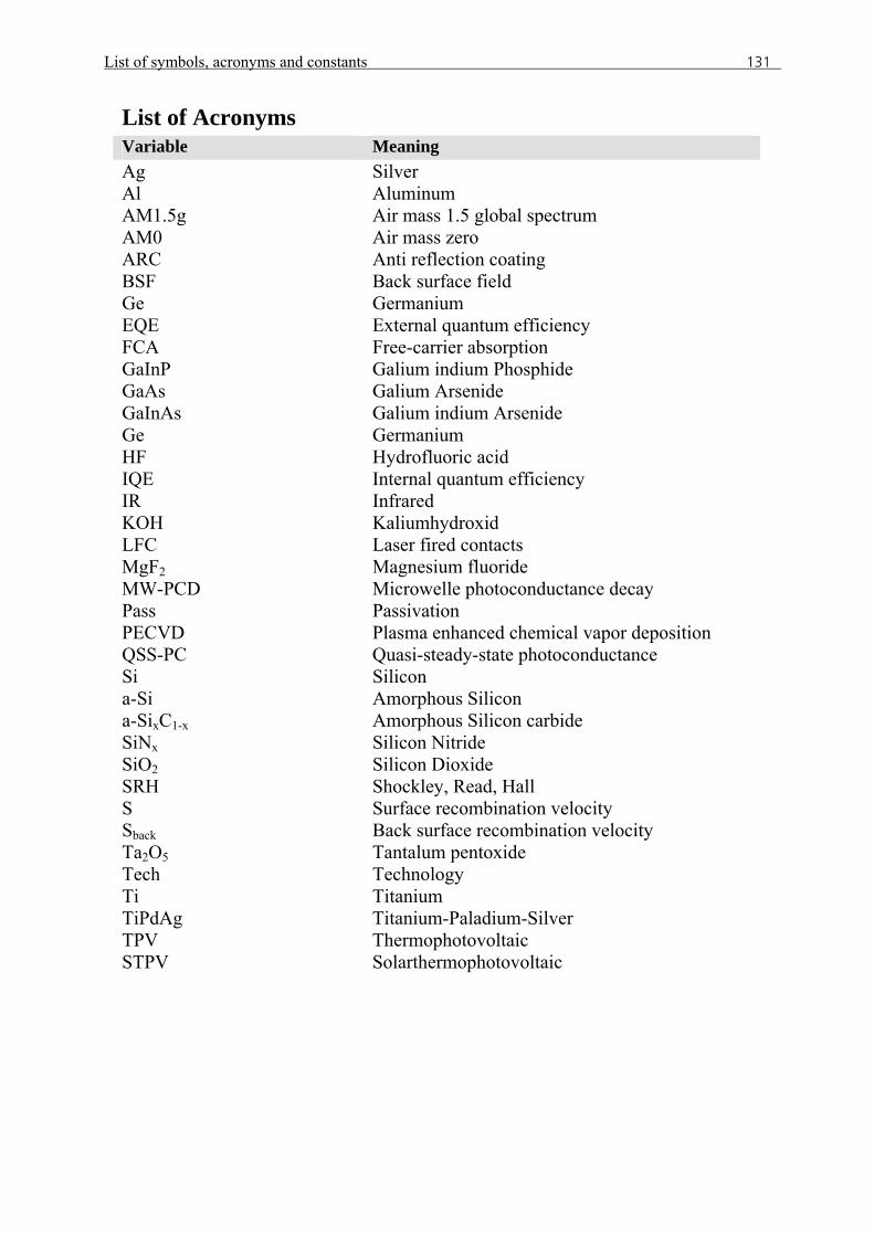
List of symbols, acronyms and constants 131
List of Acronyms Variable Meaning Ag Silver Al Aluminum AM1.5g Air mass 1.5 global spectrum AM0 Air mass zero ARC Anti reflection coating BSF Back surface field Ge Germanium EQE External quantum efficiency FCA Free-carrier absorption GaInP Galium indium Phosphide GaAs Galium Arsenide GaInAs Galium indium Arsenide Ge Germanium HF Hydrofluoric acid IQE Internal quantum efficiency IR Infrared KOH Kaliumhydroxid LFC Laser fired contacts MgF2 Magnesium fluoride MW-PCD Microwelle photoconductance decay Pass Passivation PECVD Plasma enhanced chemical vapor deposition QSS-PC Quasi-steady-state photoconductance Si Silicon a-Si Amorphous Silicon a-SixC1-x Amorphous Silicon carbide SiNx Silicon Nitride SiO2 Silicon Dioxide SRH Shockley, Read, Hall S Surface recombination velocity Sback Back surface recombination velocity Ta2O5 Tantalum pentoxide Tech Technology Ti Titanium TiPdAg Titanium-Paladium-Silver TPV Thermophotovoltaic STPV Solarthermophotovoltaic
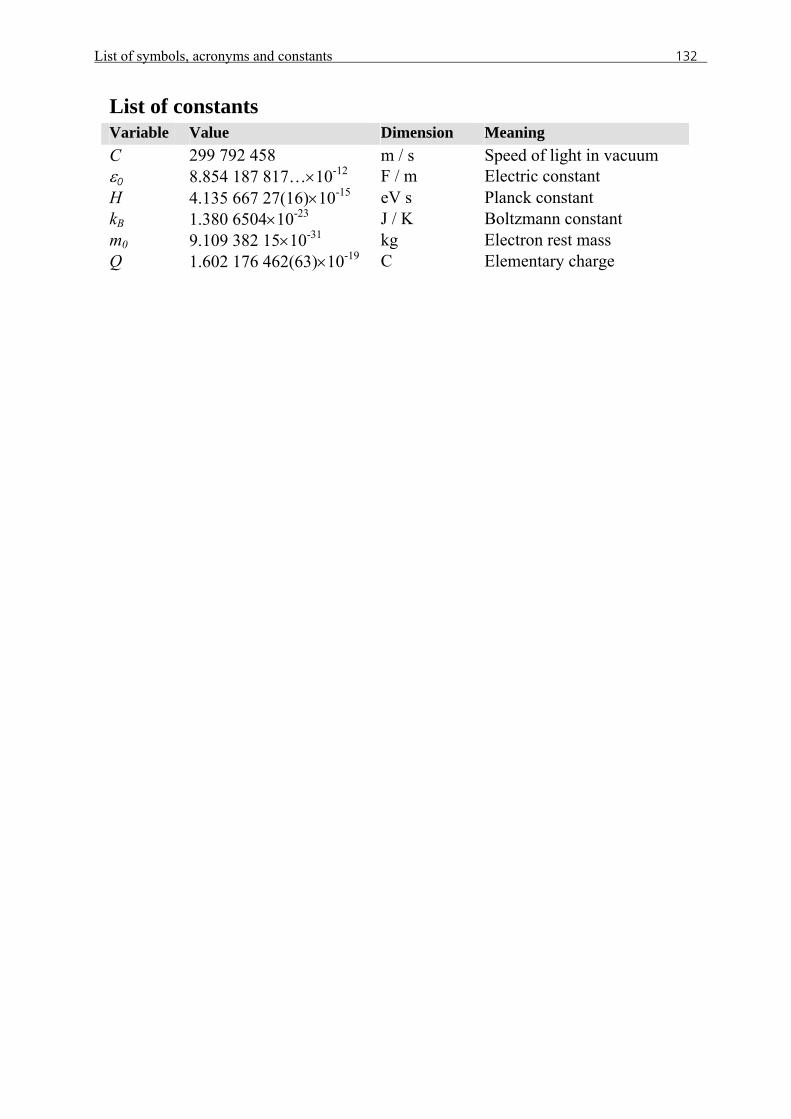
List of symbols, acronyms and constants 132
List of constants Variable Value Dimension Meaning C 299 792 458 m / s Speed of light in vacuum ε0 8.854 187 817…×10-12 F / m Electric constant H 4.135 667 27(16)×10-15 eV s Planck constant kB 1.380 6504×10-23 J / K Boltzmann constant m0 9.109 382 15×10-31 kg Electron rest mass Q 1.602 176 462(63)×10-19 C Elementary charge
List of publications 133
11 List of publications
1 J. Fernández, F. Dimroth, E. Oliva, M. Hermle and A.W. Bett, Back-surface optimiza-
tion of germanium TPV cells, Proceedings of the 7th World Conference on Thermo-
photovoltaic Generation of Electricity, El Escorial, Spain, (2006).
2 J. Fernández, F. Dimroth, E. Oliva and A.W. Bett, Development of germanium TPV
Cell Technology, Proceedings of the 22nd European Photovoltaic Solar Energy Con-
ference and Exhibition, Milan, Italy, (2007).
3 J. Fernández, S. Janz, D. Suwito, E. Oliva and F. Dimroth, Advanced Concepts for
High-Efficiency germanium Photovoltaic Cells, Proceedings of the 33rd IEEE Photo-
voltaic Specialist Conference, San Diego, USA, (2008).
4 D. Suwito, J. Fernández, J. Janz, F. Dimroth and S.W. Glunz, The influence of anneal-
ing on the passivation quality of amorphous SixC1-x on crystalline silicon and germa-
nium surfaces, Proceedings of the 34th IEEE Photovoltaic Specialist Conference,
Philadelphia (USA), (2009).
5 R. Hoheisel, J. Fernández, F. Dimroth and A. Bett, W., Analysis of Radiation Hard-
ness of Rear Surface Passivated germanium Photovoltaic Cells, Proceedings of the
34th IEEE Photovoltaic Specialist Conference, Philadelphia, USA, (2009).
6 A. Datas, C. Algora, J.C. Zamorano, V. Corregidor, D. Martin, A.W. Bett, F. Dimroth,
J. Fernández, M. Baudrit and B. Hernandez, A solar TPV system based on germanium
cells, Proceedings of the 7th World Conference on Thermophotovoltaic Generation of
Electricity, El Escorial, Spain, (2006).
7 A. Datas, V. Corregidor, D. Martin, A.W. Bett, F. Dimroth, J. Fernández and C. Al-
gora, Optimization of germanium cell arrays in tungsten emitter-based solar TPV sys-
tems, Proceedings of the Proceedings of the 7th World Conference on Thermophoto-
voltaic Generation of Electricity, Madrid, Spain, (2006).
8 R. Hoheisel, J. Fernández, F. Dimroth and A.W. Bett, Investigation of radiation hard-
ness of germanium photovoltaic cells, IEEE transactions on electron devices. 57 (9), p.
2190-4, (2010).

List of publications 134
Bibliographie 135
12 Bibliographie
[1] A. Goetzberger, B. Voß and J. Knobloch, Sonnenenergie: Photovoltaik. 2 ed, Teubner
Verlag. Stuttgart, Germany 261, (1997).
[2] J. Zhao, A. Wang and M.A. Green, Novel 19.8% efficient 'honeycomb' textured mul-
ticrystelline and 24.4% monocrystalline silicon solar cell, Applied Physics Letters. 73
(14), p. 1991-3, (1998).
[3] G. Létay and A.W. Bett, EtaOpt - a Program for Calculating Limiting Efficiency and
Optimum Bandgap Structure for Multi-Bandgap Solar Cells and TPV Cells, Proceed-
ings of the 17th European Photovoltaic Solar Energy Conference, p. 178-181, Munich,
Germany, (2001).
[4] W. Shockley and H.J. Queisser, Detailed balance limit of efficiency of p-n junction
solar cells, Journal of Applied Physics. 32 (3), p. 510-19, (1961).
[5] S.P. Philipps, W. Guter, M. Steiner, E. Oliva, G. Siefer, E. Welser, B.M. George, M.
Hermle, F. Dimroth and A.W. Bett, III-V Multi-junction Solar Cells - Simulation and
Experimental Realisation, Informacije MIDEM - Journal of Microelectronics, Elec-
tronic Components and Materials. 39 (4), p. 201-8, (2009).
[6] W. Guter, J. Schoene, S.P. Philipps, M. Steiner, G. Siefer, A. Wekkeli, E. Welser, E.
Oliva, A.W. Bett and F. Dimroth, Current-matched triple-junction solar cell reaching
41.1% conversion efficiency under concentrated sunlight, Applied Physics Letters 94
(22), p. 223504/1-3, (2009).
[7] Unpublished data, Fraunhofer ISE intern.
[8] W. Guter, Optimierung von III-V basierten Hochleistungssolarzellen, PhD thesis,
Universitaet Konstanz, (2010).
[9] S.P. Phillipps, personal communication, (2010).
[10] N.W. Ashcroft and N.D. Mermin, Solid State Physics, Saunders College, (1976).
[11] S.M. Sze, Physics of Semiconductor Devices. 2 ed, John Wiley and Sons. New York,
USA (1981).
Bibliographie 136
[12] ASTM, Standard for Terrestrial Direct Normal Solar Spectral Irradiance Tables for
Air Mass 1.5, American Society for Testing and Materials, p. 673-680, (1982).
[13] J.Aschaber, unpublished data, Fraunhofer ISE intern, (2005).
[14] Dmitri Mendeleev's predicted elements.
http://en.wikipedia.org/wiki/Dmitri_Mendeleev's_predicted_elements, (accessed Au-
gust, 2010).
[15] E.E. Haller, Germanium: From its discovery to SiGe devices Materials Science in Se-
miconductor Processing. 9 (4-5), p. 408-22, (2006).
[16] R. Bray. A History of Physics at Purdue: The War Period (1941-1945). (1990),
http://www.physics.purdue.edu/about_us/history/war_period.shtml, (accessed August,
2010).
[17] M. Riordan, The invention of the transistor, Reviews of Modern Physics. 71 (2), p.
336-45, (1999).
[18] R. Bray. The Origin of Semiconductor Research at Purdue. (1989),
http://www.physics.purdue.edu/about_us/history/semi_conductor_research.shtml, (ac-
cessed August, 2010).
[19] M.L. Lee, E.A. Fitzgerald, M.T. Bulsara, M.T. Currie and A. Lochtefeld, Strained Si,
SiGe, and Ge channels for high-mobility metal-oxide- semiconductor field-effect tran-
sistors, Journal of Applied Physics. 97 (1), p. 11101-1- 27, (2005).
[20] Computer history.
http://www.computerhistory.org/semiconductor/assets/images/400x400/1951_1_2.jpg,
(accessed August, 2010).
[21] C. Claeys and E. Simoen, Germanium-based technologies: from materials to devices,
Elsevier. Amsterdam, Netherlands (2007).
[22] R.R. Moskalyk, Review of germanium processing worldwide Minerals Engineering.
17 (3), p. 393-402, (2004).
[23] C. Kittel, Einführung in die Festkörperphysik, Oldenbourg R. Verlag GmbH, (2005).
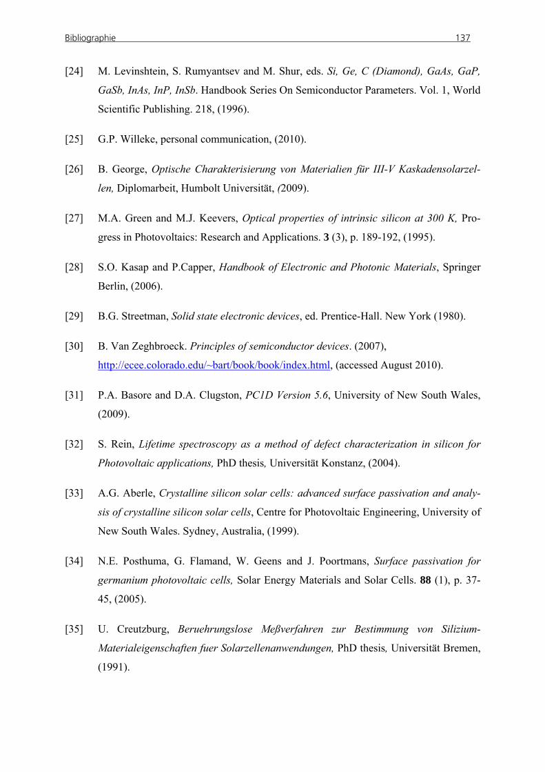
Bibliographie 137
[24] M. Levinshtein, S. Rumyantsev and M. Shur, eds. Si, Ge, C (Diamond), GaAs, GaP,
GaSb, InAs, InP, InSb. Handbook Series On Semiconductor Parameters. Vol. 1, World
Scientific Publishing. 218, (1996).
[25] G.P. Willeke, personal communication, (2010).
[26] B. George, Optische Charakterisierung von Materialien für III-V Kaskadensolarzel-
len, Diplomarbeit, Humbolt Universität, (2009).
[27] M.A. Green and M.J. Keevers, Optical properties of intrinsic silicon at 300 K, Pro-
gress in Photovoltaics: Research and Applications. 3 (3), p. 189-192, (1995).
[28] S.O. Kasap and P.Capper, Handbook of Electronic and Photonic Materials, Springer
Berlin, (2006).
[29] B.G. Streetman, Solid state electronic devices, ed. Prentice-Hall. New York (1980).
[30] B. Van Zeghbroeck. Principles of semiconductor devices. (2007),
http://ecee.colorado.edu/~bart/book/book/index.html, (accessed August 2010).
[31] P.A. Basore and D.A. Clugston, PC1D Version 5.6, University of New South Wales,
(2009).
[32] S. Rein, Lifetime spectroscopy as a method of defect characterization in silicon for
Photovoltaic applications, PhD thesis, Universität Konstanz, (2004).
[33] A.G. Aberle, Crystalline silicon solar cells: advanced surface passivation and analy-
sis of crystalline silicon solar cells, Centre for Photovoltaic Engineering, University of
New South Wales. Sydney, Australia, (1999).
[34] N.E. Posthuma, G. Flamand, W. Geens and J. Poortmans, Surface passivation for
germanium photovoltaic cells, Solar Energy Materials and Solar Cells. 88 (1), p. 37-
45, (2005).
[35] U. Creutzburg, Beruehrungslose Meßverfahren zur Bestimmung von Silizium-
Materialeigenschaften fuer Solarzellenanwendungen, PhD thesis, Universität Bremen,
(1991).
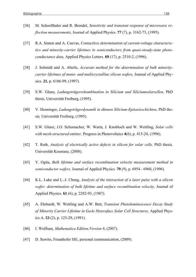
Bibliographie 138
[36] M. Schoefthaler and R. Brendel, Sensitivity and transient response of microwave re-
flection measurements, Journal of Applied Physics. 77 (7), p. 3162-73, (1995).
[37] R.A. Sinton and A. Cuevas, Contactless determination of current-voltage characteris-
tics and minority-carrier lifetimes in semiconductors from quasi-steady-state photo-
conductance data, Applied Physics Letters. 69 (17), p. 2510-2, (1996).
[38] J. Schmidt and A. Aberle, Accurate method for the determination of bulk minority-
carrier lifetimes of mono- and multicrystalline silicon wafers, Journal of Applied Phy-
sics. 21, p. 6186-99, (1997).
[39] S.W. Glunz, Ladungsträgerrekombination in Silicium und Siliciumsolarzellen, PhD
thesis, Universität Freiburg, (1995).
[40] V. Henninger, Ladungsträgerdynamik in dünnen Silicium-Epitaxieschichten, PhD the-
sis, Universität Freiburg, (1995).
[41] S.W. Glunz, J.O. Schumacher, W. Warta, J. Knobloch and W. Wettling, Solar cells
with mesh-structured emitter, Progress in Photovoltaics 4(6), p. 415-24, (1996).
[42] T. Roth, Analysis of electrically active defects in silicon for solar cells, PhD thesis,
Universität Konstanz, (2008).
[43] Y. Ogita, Bulk lifetime and surface recombination velocity measurement method in
semiconductor wafers, Journal of Applied Physics. 79 (9), p. 6954 - 6960, (1996).
[44] K.L. Luke and L.-J. Cheng, Analysis of the interaction of a laser pulse with a silicon
wafer: determination of bulk lifetime and surface recombination velocity, Journal of
Applied Physics. 61 (6), p. 2282-93, (1987).
[45] A. Ehrhardt, W. Wettling and A.W. Bett, Transient Photoluminescence Decay Study
of Minority Carrier Lifetime in GaAs Heteroface Solar Cell Structures, Applied Phys-
ics A. 53 (2), p. 123-29, (1991).
[46] I. Wolfram, Mathematica Edition.Version 6, (2007).
[47] D. Suwito, Fraunhofer ISE, personal communication, (2009).
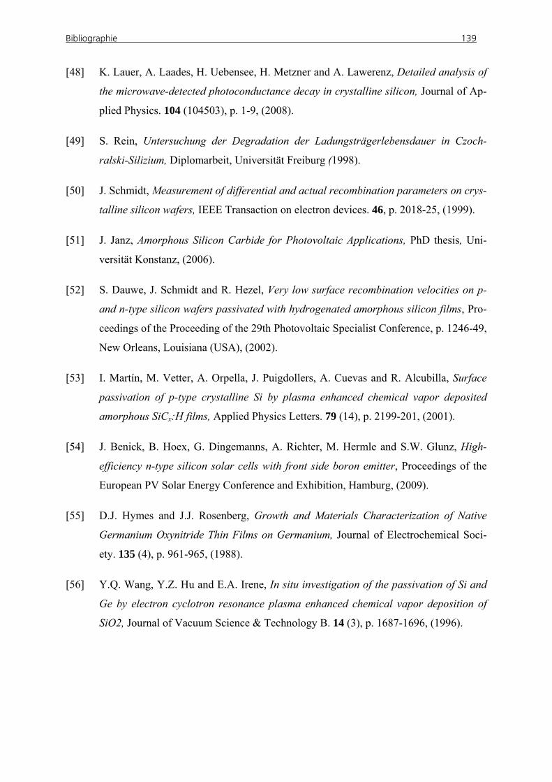
Bibliographie 139
[48] K. Lauer, A. Laades, H. Uebensee, H. Metzner and A. Lawerenz, Detailed analysis of
the microwave-detected photoconductance decay in crystalline silicon, Journal of Ap-
plied Physics. 104 (104503), p. 1-9, (2008).
[49] S. Rein, Untersuchung der Degradation der Ladungsträgerlebensdauer in Czoch-
ralski-Silizium, Diplomarbeit, Universität Freiburg (1998).
[50] J. Schmidt, Measurement of differential and actual recombination parameters on crys-
talline silicon wafers, IEEE Transaction on electron devices. 46, p. 2018-25, (1999).
[51] J. Janz, Amorphous Silicon Carbide for Photovoltaic Applications, PhD thesis, Uni-
versität Konstanz, (2006).
[52] S. Dauwe, J. Schmidt and R. Hezel, Very low surface recombination velocities on p-
and n-type silicon wafers passivated with hydrogenated amorphous silicon films, Pro-
ceedings of the Proceeding of the 29th Photovoltaic Specialist Conference, p. 1246-49,
New Orleans, Louisiana (USA), (2002).
[53] I. Martín, M. Vetter, A. Orpella, J. Puigdollers, A. Cuevas and R. Alcubilla, Surface
passivation of p-type crystalline Si by plasma enhanced chemical vapor deposited
amorphous SiCx:H films, Applied Physics Letters. 79 (14), p. 2199-201, (2001).
[54] J. Benick, B. Hoex, G. Dingemanns, A. Richter, M. Hermle and S.W. Glunz, High-
efficiency n-type silicon solar cells with front side boron emitter, Proceedings of the
European PV Solar Energy Conference and Exhibition, Hamburg, (2009).
[55] D.J. Hymes and J.J. Rosenberg, Growth and Materials Characterization of Native
Germanium Oxynitride Thin Films on Germanium, Journal of Electrochemical Soci-
ety. 135 (4), p. 961-965, (1988).
[56] Y.Q. Wang, Y.Z. Hu and E.A. Irene, In situ investigation of the passivation of Si and
Ge by electron cyclotron resonance plasma enhanced chemical vapor deposition of
SiO2, Journal of Vacuum Science & Technology B. 14 (3), p. 1687-1696, (1996).
Bibliographie 140
[57] V. Andreev, V. Khvostikov, V. Kalinovsky, V. Lantratov, V. Grilikhes, V. Rumyant-
sev, M. Shvarts, V. Fokanov and A. Pavlov, High Current Density GaAs And GaSb
Photovoltaic Cells For Laser Power Beaming, Proceedings of the Proceedings of the
3rd World Conference on Photovoltaic Energy Conversion, p. 761-64, Osaka, Japan,
(2003).
[58] M.A. Lieberman and A.J. Lichtenberg, Principles of plasma discharges and materials
processing, John Wiley & Sons, Inc. 572, (1994).
[59] J. Rentsch, Trockentechnologien zur Herstellung von kristallinen Siliziumsolarzellen,
PhD thesis, Albert-Ludwigs Universität, Freiburg, (2005).
[60] S. Schaefer, Plasmaätzen für die Photovoltaik: Plasmasysteme und -Prozesse für die
Herstellung von kristallinen Siliziumsolarzellen, PhD thesis, Universität Konstanz,
(2000).
[61] M. Hofmann, Rear surface conditioning and passivation for locally contacted crystal-
line silicon solar cells, PhD thesis, Universität Konstanz, (2008).
[62] N. Posthuma, Highly efficient thin Germanium bottom cells for mechanically stacked
photovoltaic devices, PhD thesis, Katholieke Universiteit Leuven, (2006).
[63] S. Sun, Y. Sun, Z. Liu, D. Lee, S. Peterson and P. Pianetta, Surface termination and
roughness of Ge (100) cleaned by HF and HCl solutions, Applied Physics Letters. 88
(021903), (2006).
[64] D. Suwito, J. Fernandez, J. Janz, F. Dimroth and S.W. Glunz, The influence of anneal-
ing on the passivation quality of amorphous SixC1-x on crystalline silicon and germa-
nium surfaces, Proceedings of the 34th IEEE Photovoltaic Specialist Conference, p.
700-04, Philadelphia (USA), (2009).
[65] R. Stangl, M. Kriegel and M. Schmidt, AFORS-HET, Version 2.2, a Numerical Com-
puter Program for Simulation of Heterojunction Solar cells and Measurements, Pro-
ceedings of the 4th World Conference on Photovoltaic Energy Conversion, p. 1350-3,
Waikoloa, Hawaii, USA, (2006).
[66] S.W. Glunz, Band gap narrowing in p-type base regions of solar cells, Proceedings of
the 17th European Photovoltaic Solar Energy Conference, Munich (Germany), (2001).
Bibliographie 141
[67] W. van Roosbroeck and W. Shockley, Photon-radiative recombination of electrons
and holes in Germanium, Physical Review. 94 (6), p. 1558-1560, (1954).
[68] P.H. Brill and R.F. Schwarz, Radiative recombination and lifetime in germanium,
Journal of Physics and Chemistry of Solids. 8, p. 75-77, (1959).
[69] Y.P. Varshni, Band-to-Band Radiative Recombination in Groups IV, VI, and III-V
Semiconductors (I), physica status solidi (b). 19 (2), p. 459-514, (1967).
[70] R. Conradt and J. Aengenheister, Minority carrier lifetime in highly doped Ge, Solid
State Communications. 10 (3), p. 321-323 (1972).
[71] L. Huldt, Phonon-assisted Auger recombination in germanium, Physica Status Solidi
(a). 33 (2), p. 607-614, (1976).
[72] D.K. Schroder, Semiconductor Material and Device Characterization, John Wiley &
Sons. New York 599, (1990).
[73] D. Poelman, P. Clauws and B. Depuydt, Chemical surface passivation of low resistiv-
ity p-type Ge wafers for solar cell applications, Solar Energy Materials and Solar
Cells. 76 (2), p. 167-73, (2003).
[74] T.J. Coutts, A review of progress in thermophotovoltaic generation of electricity, Re-
newable and Sustainable Energy Reviews, (3), p. p. 77-184, (1999).
[75] A. Datas and C. Algora, Analytical model of solar thermophotovoltiac systems with
cylindrical symmetry:Ray tracing approach, Progress in Photovoltaics. 17, p. 526-541,
(2009).
[76] T. Schlegl, GaSb-Photovoltaikzellen für die Thermophotovoltaik, PhD thesis, Univer-
sität Regensburg, (2005).
[77] A. Datas, personal communication, (2010).
[78] V.M. Andreev, V.P. Khvostikov, O.A. Khvostikova, A.S. Vlasov, P.Y. Gazaryan,
N.A. Sadchikov and V.D. Rumyantsev, Solar thermophotovoltaic system with high
temperature tungsten emitter, Proceedings of the 31st IEEE Photovoltaic Specialists
Conference, p. 671-674, Orlando, Florida, USA, (2005).
Bibliographie 142
[79] A.S. Vlasov, V.P. Khvostikov, O.A. Khovostikova, P.Y. Gazaryan, S.V. Sorokina and
V.M. Andreev, TPV Systems with Solar Powered Tungsten Emitter, Proceedings of
the 7th Conference on Thermophotovoltaic Generation of Electricity, p. 327-334, San
Lorenzo de El Escorial, Madrid, (2006).
[80] K. Qiu, A.C.S. Hayden, M.G. Mauk and O.V. Sulima, Generation of electricity using
InGaAsSb and GaSb TPV cells in combustion-driven radiant sources Solar Energy
Materials and Solar Cells. 90 (1), p. 68-81, (2006).
[81] N. Jovanovic, I. Celanovic and J. Kassakian, Two-dimensional Tungsten Photonic
Crystals as Thermophotovoltaic Selective Emitters, Proceedings of the 7th World Con-
ference on Thermophotovoltaic Generation of Electricity, p. 47-55, El Escorial, Spain,
(2006).
[82] H. Sai, T. Kamikawa, Y. Kanamori, K. Hane, H. Yugami and M. Yamaguchi, Ther-
mophotovoltaic generation with microstructured tungsten selective emitters, Proceed-
ings of the 6th Conference on Thermophotovoltaic Generation of Electricity, p. 206-
214, Freiburg, (2004).
[83] A. Datas, C. Algora, J.C. Zamorano, V. Corregidor, D. Martin, A.W. Bett, F. Dimroth,
J. Fernandez, M. Baudrit and B. Hernandez, A solar TPV system based on germanium
cells, Proceedings of the 7th World Conference on Thermophotovoltaic Generation of
Electricity, p. 280-90, El Escorial, Spain, (2006).
[84] V.P. Khvostikov, O.A. Khvostikova, P.Y. Gazaryan, S.V. Sorokina, N.S. Potapovich,
A.V. Malevskaya, M.Z. Shvarts, N.A. Kaluzhniy, V.M. Andreev and V.D. Rumyant-
sev, Photoconverters for Solar TPV Systems, Proceedings of the 4th World Confer-
ence on Photovoltaic Energy Conversion, p. 667-70, Waikoloa, Hawaii, USA, (2006).
[85] T. Nagashima, K. Hokoi, K. Okumura and M. Yamaguchi, Surface Passivation for
Germanium and Silicon Back Contact Type Photovoltaic Cells, Proceedings of the 4th
World Conference on Photovoltaic Energy Conversion, p. 655-8, Waikoloa, Hawaii,
USA, (2006).
[86] N.E. Posthuma, J. Van der Heide, G. Flamand and J. Poortmans, Recent Procress in
the Development of a Stand-Alone Germanium Solar Cell, Proceedings of the 21st Eu-
ropean Photovoltaic Solar Energy Conference, p. 137-40, Dresden, Germany, (2006).
Bibliographie 143
[87] J. van der Heide, Cost-efficient thermophotovoltaic cells based on germanium, PhD
thesis, Katholieke Universiteit Leuven, (2009).
[88] M. Meusel, Entwicklung von III-V Mehrfach-Solarzellen für die Anwendung im Welt-
raum, PhD thesis, Universität Konstanz, (2007).
[89] S.W. Glunz, A.Grohe, M.Hermle, M.Hoffmann, S.Janz, T.Roth, O.Schulz, M.Vetter,
I.Martin, R.Ferre, S.Bermejo, W.Wolke, W.Warta, R.Preu and HG.Willeke, Compari-
son of different dielectric passivation layers for application in industrially feasible
high-efficiency crystalline silicon solar cells, Proceedings of the European Photovol-
taic Solar Energy Conference and Exhibition, Barcelona, Spain, (2005).
[90] E. Schneiderloechner, R. Preu, R. Lüdemann and S.W. Glunz, Laser-fired rear con-
tacts for crystalline silicon solar cells, Progress in Photovoltaics. 10, p. 29-34, (2002).
[91] B.George, Unpublished data. Fraunhofer ISE intern, 2010.
[92] M. Breselge, Simulation von III-V Kaskadensolarzellen und Charakterisierung opti-
scher Materialparameter, Diplomarbeit, Freiburg, Germany, (2003).
[93] R. Loeckenhoff, Neue Aufbau- und Integrationstechniken für die hoch konzentrierende
Photovoltaik, PhD thesis, Albert-Ludwigs-Universität Freiburg, (2007).
[94] A. Kaminski, B. Vandelle, A. Fave, J.P. Boyeaux, L.Q. Nam, R. Monna, D. Sarti and
A. Laugier, Aluminium BSF in silicon solar cells, Solar Energy Materials and Solar
Cells. 72 (1-4), p. 373-379, (2001).
[95] K. Haas, Analyse des transienten Verhaltens von Photovoltaik- Zellen, Diplomarbeit,
Freiburg, Germany, (1997).
[96] ISO, Space systems - Space solar cells - Requirements, measurements and calibration
procedures, 15387, p. 1-78, (2005).
[97] M.A. Green, Solar Cells, Operating Principles, Technology, and System Applications,
(1982).
[98] M.D. Archer and R. Hill, Clean Electricity from Photovoltaics, World Scientific Pub-
lishing Company, (2001).
Bibliographie 144
[99] C. Baur, Entwicklung und Charakterisierung von III-V Weltraumsolarzellen, PhD the-
sis, Universität Konstanz, (2007).
[100] J. Fernández, S. Janz, D. Suwito, E. Oliva and F. Dimroth, Advanced Concepts for
High-Efficiency Germanium Photovoltaic Cells, Proceedings of the 33rd IEEE Photo-
voltaic Specialist Conference, p. 1-4, San Diego, USA, (2008).
[101] R. Hoheisel, J. Fernández, F. Dimroth and A.W. Bett, Analysis of Radiation Hardness
of Rear Surface Passivated Germanium Photovoltaic Cells, Proceedings of the 34th
IEEE Photovoltaic Specialist Conference, p. 861-864, Philadelphia, USA, (2009).
[102] R. Hoheisel, J. Fernández, F. Dimroth and A.W. Bett, Investigation of radiation hard-
ness of germanium photovoltaic cells, IEEE transactions on electron devices. 57 (9), p.
2190-4, (2010).
[103] D. Suwito, Intrinsic and doped amorphous silicon carbide for the surface passivation
of silicon solar cells, PhD thesis, Universität Konstanz, (2010).
[104] B. Hoex, J. Schmidt, P. Pohl, M.C.M. van de Sanden and W.M.M. Kessels, Silicon
surface passivation by atomic layer deposited Al2O3, Journal of Applied Physics. 104
(044903), (2008).
[105] E.Gaubas, personal communication, (2008).
[106] D. Grote, Analyse und Modellierung lateral variierender Eingenschaften industriel
hergestellter Solarzellen, Diplomarbeit, Universität Freiburg, (2004).
[107] Instruction manual of Fourier spectrometer IFS66 Bruker,
[108] R. Hoheisel, Charakterisierung und Optimierung von hoch-effizienten III-V Welt-
raumsolarzellen: Strahlungsresistenz, Spektrum- und Temperaturabhängigkeit, PhD
thesis, Universität Konstanz, (2010).
[109] M. Meusel, C. Baur, G. Siefer, F. Dimroth, A.W. Bett and W. Warta, Characterization
of monolithic III-V multi-junction solar cells- challenges and application, Solar En-
ergy Materials and Solar Cells. 90 (18-19), p. 3268-75, (2006).


![Development in Thermoforming Thermoplastic Composites FINAL · PPS Semi-crystalline 89 307 325 $ PEKK Semi-crystalline 156 306 340 $$ Table1.Common’thermoplastics’used’in’composites’[9,10]](https://img.pdfslide.net/doc/110x75/5e5f7df8ff929812ef50b3bb/development-in-thermoforming-thermoplastic-composites-final-pps-semi-crystalline.jpg)