Embed Size (px)
Citation preview
DEVELOPMENT OF PROTECTIVE
NANO-COATINGS FOR ELECTRO-OPTICAL
SYSTEMS
A Thesis Submitted to
The Graduate School of Engineering and Sciences of
Izmir Institute of Technology
In Partial Fulfillment of the Requirements for the Degree of
MASTER OF SCIENCE
in Chemical Engineering
by
Merve ÖZPİRİN
July 2016
İZMİR
We approve the thesis of Merve ÖZPİRİN
Examining Committee Members:
__________________________________
Assist. Prof. Dr. Özgenç EBİL
Department of Chemical Engineering, Izmir Institute of Technology
__________________________________
Prof. Dr. Mustafa M. DEMİR
Department of Material Science and Engineering, Izmir Institute of Technology
__________________________________
Assist. Prof. Dr. Güler NARİN
Department of Chemical Engineering, Usak University
13 July 2016 ____________________________________ ____________________________________ ___________________________________
Assist. Prof. Dr. Özgenç EBİL Supervisor, Department of Chemical
Engineering, Izmir Institute of Technology
Prof. Dr. S. Fehime ÇAKICIOĞLU
ÖZKAN
Head of the Department of Chemical
Engineering
Prof. Dr. Bilge KARAÇALI
Dean of the Graduate School of
Engineering and Sciences

ACKNOWLEGEMENTS
I am sincerely thankful to people who helped me in my M.Sc. thesis.
Initially, I would like to express my thankfulness to my supervisor, Assist. Prof.
Dr. Özgenç EBİL that he provides me opportunities to work on the TUBITAK project,
for his knowledge, encouragement, guidance, perceptiveness, precious advices during my
study, many valuable and good ideas that offered me on my thesis subject, and his endless
support to complete my M.Sc. thesis.
I would also like to thank my friends; especially Gizem PAYER, Sema KIRKÖSE
and Selcan ATEŞ for their help in laboratory works and also their friendship.
I wish to thank Dr. Hüseyin ÖZGENER, Zeynep AY, Aysel TOMAK and staff at
Center for Materials Research in Izmir Institute of Technology for their help in
characterizations.
I am grateful and I express my special thanks to Emre DEMİRKAYA for his
understanding, motivations which contribute to me in my work, limitless support ensured
to my life, sincerity, friendship and helping me throughout my M.Sc. thesis.
Finally, I would especially like to thank and express my gratitude to my family
because they always listen to me and show me the right ways for my future and also thank
for their supports in every sense to overcome difficult times, understanding, motivations
and valuable opinions.
iv
ABSTRACT
DEVELOPMENT OF PROTECTIVE NANO-COATINGS FOR
ELECTRO-OPTICAL SYSTEMS
Electro-optical (EO) systems have wide range of applications and in recent years,
especially the use of EO imaging systems in military and civil aviation applications have
substantially increased. In these applications, EO systems are exposed to quite harsh and
unstable operating conditions like sudden changes in temperature and humidity, dust, fog,
physical shock, vibration and radiation. If their optical surfaces such as prisms, lenses and
mirrors are damaged due to these conditions, their repair usually is not possible. To
overcome these problems, it is necessary to develop special protective coating layers for
optical surfaces.
The main goal of this study is to produce protective, self-cleaning and super-
hydrophobic polymeric thin films for optical surfaces of the electro-optical (EO) systems.
Initiated chemical vapor deposition (iCVD) is a novel method for the fabrication of thin
film coatings and it has many advantages such as low production cost, very low deposition
temperature, 3D geometry coating performance and high deposition rate. Therefore,
iCVD was employed to fabricate homopolymers of poly (glycidyl methacrylate) (PGMA)
and poly (1H, 1H, 2H, 2H-Perfluorodecyl acrylate) (PPFDA) and P(GMA-PFDA)
copolymer thin-films as protective coatings for EO systems.
Optical modeling and simulations were performed to determine the effect of film
thickness and refractive index on optical performance of substrates to be coated. Optical
performance of fabricated coatings was also measured between 400 and 1000 nm range
to confirm that protective coatings do not have any measureable impact on optical
performance provided that the protective film thickness is kept between 50 nm to 1 µm.
The surface morphology of the protective coatings was evaluated using a variety of
analytical tools such as Fourier Transform Infrared Spectroscopy (FTIR), Scanning
Electron Microscopy (SEM), Atomic Force Microscopy (AFM) and Contact Angle
measurements. Optical tests were performed by following MIL-F-48616 Military
Standard (MIL-STD). The best protective coatings were obtained by using P(GMA-
PFDA) copolymer which yields good mechanical properties due to epoxy pendant group
and super hydrophobicity due to incorporation of fluoro monomer.
v
ÖZET
ELEKTRO-OPTİK SİSTEMLER İÇİN KORUYUCU NANO
KAPLAMALARIN GELİŞTİRİLMESİ
Elektro-optik (EO) sistemler çok geniş uygulama alanlarına sahiplerdir, son
yıllarda, özellikle Elektro-optik görüntüleme sistemlerinin askeri ve sivil havacılık
sektöründe kullanımı oldukça artmıştır. Bu alanlarda EO sistemler anlık sıcaklık
değişimi, nem, toz, sis, fiziksel şok, titreşim ve radyasyon gibi oldukça zorlu ve değişken
çalışma koşullarına maruz kalmaktadırlar. Bu sistemlerin sahip olduğu prizma, lens ve
ayna gibi optik yüzeyler, bu şartlardan dolayı zarar görürlerse, tamirleri neredeyse
mümkün olmamakta ve bu tip karşılaşılan problemlerin çözümlenebilmesi amacıyla,
optik yüzeyler için özel koruyu kaplamaların geliştirilmesine gerek duyulmaktadır.
Bu çalışmanın asıl amacı, EO sistemlerin optik yüzeyleri için koruyucu, kendi
kendini temizleyebilen, süperhidrofobik polimerik ince filmlerin üretilmesidir.
Başlatılmış Kimyasal Buhar Biriktirme (BKBB) yöntemi, ince film kaplamalarının
üretimesinde kullanılan oldukça yeni bir yöntemdir ve düşük üretim maaliyeti, düşük
sıcaklık koşulları, üç boyutlu yüzeyleri kaplama performansı ve yüksek biriktirme hızı
gibi bir çok avantaja sahiptir. Bu nedenle, BKBB yöntemi kullanılarak EO sistemler için
Poli(glisidil metakrilat) (PGMA) ve Poli(1H, 1H, 2H, 2H-Perflorodesil akrilat) (PPFDA)
homopolimerleri ve P(GMA-PFDA) kopolimer ince filmlerinin üretimi yapılmıştır.
Film kalınlığı ve kırılma indisinin kaplanacak yüzeylerin optik performansına
etkisini incelemek için optik modelleme ve simülasyonlar yapılmış bunun yanında film
kalınlığı 50 nm ile 1 µm arasında tutularak üretilen koruyucu kaplamaların optik
performansa herhangi bir etkisinin olmadığını doğrulamak amacıyla, kaplamaların 400-
1000 nm aralığında ölçümleri alınmıştır. Koruyucu kaplamaların yüzey morfolojisinin
belirlenmesi, Fourier Dönüşümlü Kızılötesi (FTIR) Spektroskopisi, Taramalı Elektron
Mikroskobu (SEM), Atomik Güç Mikroskobu (AFM) ve Değme Açı ölçümü gibi çeşitli
analitik tekniklerin kullanılması ile gerçekleştirilmiştir. Ayrıca, MIL-F-48616 askeri
standardı (MIL-STD) takip edilerek optik testler yapılmıştır. Sonuç olarak, en iyi
koruyucu kaplama hem yapısındaki epoksi grubundan dolayı iyi mekanik özellik gösterip
hem de fluoro monomerin sağladığı süperhidrofobik özelliğe sahip olduğu için P(GMA-
PFDA) kopolimeriyle elde edilmiştir.
vi
TABLE OF CONTENTS
LIST OF FIGURES ......................................................................................................... ix
LIST OF TABLES ......................................................................................................... xiii
CHAPTER 1. INTRODUCTION ..................................................................................... 1
1.1. Electro-Optical (EO) Systems ............................................................ 1
1.2. Optical Coating Technology and Applications .................................. 3
1.2.1. Optical Materials and Their Properties ........................................ 4
1.2.1.1. Light Interactions with Materials .......................................... 6
1.2.1.2. Crystalline Materials ........................................................... 11
1.2.1.3. Optical Glass Materials ....................................................... 14
1.2.1.4. Polymeric Materials .......................................................... 18
1.2.1.5. Metals .................................................................................. 21
1.2.2. Optical Coating Techniques ....................................................... 23
1.2.2.1. Antireflection Coating ......................................................... 24
1.2.2.2. High Reflection Coating ..................................................... 25
1.2.2.3. Partial Reflectors ................................................................. 27
1.2.2.4. Optical Filters ...................................................................... 27
1.2.3. Thin Film Production Methods .................................................. 28
1.2.3.1. Initiated Chemical Vapor Deposition (iCVD) .................... 32
CHAPTER 2. EXPERIMENTAL WORK ..................................................................... 43
2.1. iCVD System.................................................................................... 43
2.2. Materials ........................................................................................... 44
2.3. Cleaning Procedures of the Substrates ............................................. 46
2.4. Polymeric Thin Film Coating Procedure in iCVD System .............. 48
2.4.1. Startup of Thin Film Coating in iCVD System ......................... 48
2.4.2. Operating Mode in iCVD System .............................................. 49
2.4.3. Shutdown Procedure in iCVD System ....................................... 49
2.5. Characterization ............................................................................... 50
vii
CHAPTER 3. MODELING OF OPTICAL COATINGS ............................................... 52
CHAPTER 4. RESULTS AND DISCUSSION .............................................................. 69
4.1. PGMA Deposition in iCVD System ................................................ 69
4.1.1. Thickness Measurement with Reflectometer for PGMA Coatings
...……………………………………………………………………...74
4.1.2. FTIR Analysis of GMA Monomer and PGMA Film................. 75
4.1.3. SEM Analysis of PGMA Film ................................................... 77
4.1.4. AFM Results of PGMA Film ..................................................... 78
4.1.5. Contact Angle Measurement for PGMA Film ........................... 80
4.1.6. Surface Quality Test with Optical Microscopy for PGMA Film…
……………………………………...………………………………. ..80
4.2. PPFDA Deposition in iCVD System ............................................... 81
4.2.1. Thickness Measurement with Reflectometer for PPFDA Coatings
…………………………………………………………………….. ....84
4.2.2. FTIR Analysis of PFDA Monomer and PPFDA Film ............... 86
4.2.3. SEM Analysis of PPFDA Film .................................................. 87
4.2.4. AFM Results of PPFDA Film .................................................... 88
4.2.5. Contact Angle Measurement for PPFDA Film .......................... 89
4.2.6. Surface Quality Test with Optical Microscopy for PPFDA Film…
………………………………………………………………...……. ..90
4.3. Copolymer P(GMA-PFDA) Deposition in iCVD System ............... 91
4.3.1. Thickness Measurement with Reflectometer for Copolymer Films
……………………………………………………………...………. ..92
4.3.2. FTIR Analysis of Copolymer Films .......................................... 93
4.3.3. SEM Analysis of Copolymer Films ........................................... 94
4.3.4. AFM Results of Copolymer P(GMA-PFDA) Films .................. 95
4.3.5. Contact Angle Measurement for Copolymer Films ................... 96
4.3.6. Surface Quality Test for Copolymer P(GMA-PFDA) Films ..... 97
4.4. Performance Tests for Homopolymer and Copolymer Films .......... 98
4.4.1. Humidity Test ............................................................................ 98
4.4.2. Swelling-Solubility in Water Test ........................................... 100
4.4.3. Salt Solubility Test ................................................................... 101
4.4.4. Solubility and Cleanability Test............................................... 103

viii
4.4.5. Adhesion Test .......................................................................... 103
CHAPTER 5. CONCLUSIONS ................................................................................... 106
REFERENCES ............................................................................................................. 108
ix
LIST OF FIGURES
Figure Page
Figure 1.1. An electromagnetic wave having electric field E, magnetic field B and the
wavelength λ ................................................................................................. 4
Figure 1.2. Regions of electromagnetic spectrum ............................................................ 5
Figure 1.3. Refraction of light .......................................................................................... 6
Figure 1.4. Absorption mechanism of a photon ................................................................ 8
Figure 1.5. The electric field components; p-polarization and s-polarization ................ 10
Figure 1.6. Constructive and destructive wave interference ........................................... 24
Figure 1.7. Schematic representation of a single layer antireflection coating ................ 24
Figure 1.8. Multilayer film that has quarter wavelength thicknesses ............................. 25
Figure 1.9. Reflectance curve of dielectric film stack .................................................... 26
Figure 1.10. Atomic layer deposition (ALD) process steps ........................................... 31
Figure 1.11. Schematic illustration of spin coating process ........................................... 32
Figure 1.12. Initiated chemical vapor deposition (iCVD) system .................................. 34
Figure 1.13. General mechanism of iCVD technique ................................................... 36
Figure 1.14. iCVD reaction mechanism, I: initiator, M: monomer, R: radical ............. 36
Figure 2.1. Vacuum chamber of iCVD system ............................................................... 44
Figure 2.2. RCA cleaning procedure for c-Si substrates ................................................ 47
Figure 2.3. Cleaning procedure for glass substrates ....................................................... 48
Figure 2.4. General substrate coating scheme in iCVD system ...................................... 50
Figure 2.5. Mprobe-Vis system ...................................................................................... 50
Figure 3.1. Transmission curves of substrate materials .................................................. 53
Figure 3.2. Film stack model of 1 pair PTFE/PMMA .................................................... 54
Figure 3.3. Transmission graphs of 1 layer-100 nm PTFE/100 nm PMMA (black) and
10 layer-150 nm PTFE/150 nm PMMA (red) on sapphire substrates ......... 55
Figure 3.4. Film stack model of 10 pair PTFE/PMMA .................................................. 55
Figure 3.5. Transmission graphs of 10 layer-100 nm PTFE/100 nm PMMA (black)and
10 layer-150 nm PTFE/150 nm PMMA (red) on sapphire substrates ........56
Figure 3.6. Film stack model of 100 pair PTFE/PMMA ................................................ 56
Figure 3.7. Transmission graphs of 100 layer-100 nm PTFE/100 nm PMMA (black)
and 100 layer-150 nm PTFE/150 nm PMMA (red) on sapphire substrates. 57
x
Figure 3.8. BK7 transmission behavior (transmission scale between 95-96%) ............. 59
Figure 3.9. Simulation graphs of modeling BK7 coated with different thickness of
PGMA ........................................................................................................... 60
Figure 3.10. Transmission graph of BK7 coated with PGMA from 50 nm to 1µm ....... 61
Figure 3.11. Transmission graph of BK7 coated with FP from 50 nm to 1µm .............. 62
Figure 3.12. Transmission graph of BK7 coated with copolymer (PGMA-FP) from 50
nm to 1 µm ................................................................................................. 63
Figure 3.13. Microscope slide transmission curve ......................................................... 64
Figure 3.14. Transmission graph of MS coated with PGMA from 50 nm to 1µm ......... 65
Figure 3.15. Transmission graph of MS coated with FP from 50 nm to 1µm ................ 66
Figure 3.16. Transmission graph of Microscope slide coated with copolymer (PGMA-
FP) from 50 nm to 1 µm ............................................................................ 66
Figure 3.17. Transmission graph of BK7 coated with Si3N4 from 50 nm to 1µm .......... 67
Figure 3.18. Transmission graph of MS coated with Si3N4 from 50 nm to 1µm ........... 68
Figure 4.1. Glycidyl methacrylate (GMA) structure ...................................................... 69
Figure 4.2. Calibration graphs of GMA in MFC2 and MMFC and TBPO in MFC1 and
MFC3 ............................................................................................................ 71
Figure 4.3. Reflectometer results of (a) iCVD61, (b) iCVD40 and (c) iCVD53
depositions for PGMA coatings on c-Si ....................................................... 74
Figure 4.4. FTIR spectra of (a) GMA monomer and (b) PGMA film synthesized in
iCVD system ................................................................................................. 76
Figure 4.5. SEM images of (a) uncoated c-Si substrate (b) c-Si coated with ~1 µm
PGMA Film .................................................................................................. 77
Figure 4.6. AFM results of bare c-Si substrate (a) color map (b) 3D view .................... 78
Figure 4.7. AFM color map and 3D images of PGMA coating with (a) ~500 nm and (b)
1 µm thickness .............................................................................................. 79
Figure 4.8. Contact angle results for bare c-Si substrate and c-Si coated with ~500 nm
PGMA film ................................................................................................... 80
Figure 4.9. Surface images of 1µm PGMA film at (a) 40x and (b) 80x magnifications. 81
Figure 4.10. 1H, 1H, 2H, 2H, (Perfluorodecyl) acrylate (PFDA) structure ................... 81
Figure 4.11. Calibration result of PFDA in MFC2 ......................................................... 82
Figure 4.12. Reflectometer results of (a) iCVD73, (b) iCVD69 and (c) iCVD72
depositions for PPFDA coatings on c-Si ................................................... 85
xi
Figure 4.13. FTIR spectra of (a) PFDA monomer and (b) PPFDA film synthesized in
iCVD system .............................................................................................. 86
Figure 4.14. SEM image of c-Si coated with 352 nm PPFDA film ............................... 87
Figure 4.15. SEM images of (a) uncoated napkin (b) coated napkin with PPFDA film..88
Figure 4.16. AFM color map and 3D images of PPFDA coating with (a) medium
thickness 352 nm and (b) 1.09 µm thickness ............................................. 89
Figure 4.17. Contact angle results for bare c-Si substrate and c-Si coated with 1.09 µm
PPFDA coating .......................................................................................... 90
Figure 4.18. Surface images of 1.09 µm PPFDA film at (a) 40x and (b) 80x
magnifications ............................................................................................ 91
Figure 4.19. Reflectometer result of (a) iCVD59 and (b) iCVD77 depositions for
Copolymer coatings on c-Si ....................................................................... 92
Figure 4.20. FTIR spectra of (a) homopolymer PGMA, (b) homopolymer PPFDA, (c)
copolymer P(GMA-PFDA) deposited in iCVD59 and (d) copolymer
P(GMA-PFDA) deposited in iCVD77 ....................................................... 93
Figure 4.21. SEM image of c-Si coated with copolymer P(GMA-PFDA) film which
contains higher amount of PGMA ............................................................. 94
Figure 4.22. SEM image of c-Si coated with copolymer P(GMA-PFDA) film which
contains higher amount of PPFDA ............................................................ 95
Figure 4.23. AFM color map and 3D images of copolymer coatings synthesized in (a)
iCVD59 run and (b) iCVD77 run .............................................................. 95
Figure 4.24. Contact angle results for c-Si substrate coated with copolymer films ....... 97
Figure 4.25. Surface images of (a) iCVD59 and (b) iCVD77 deposition samples at 80x
magnification ............................................................................................. 97
Figure 4.26. Thickness and reflection inspection of PGMA film produced in iCVD
system before and after humidity test ........................................................ 99
Figure 4.27. Thickness and reflection inspection of PGMA film produced in iCVD
system before and after swelling-solubility in water test ........................ 101
Figure 4.28. Thickness and reflection inspection of PGMA film produced in iCVD
system before and after salt solubility test ............................................... 102
Figure 4.29. Thickness measurement results before and after adhesion test for (a)
Copolymer (iCVD59) and (b) Copolymer (iCVD77) films produced in
iCVD system ............................................................................................ 104

xii
Figure 4.30. Before and after adhesion test visual inspection results of (a) and (b)
Copolymer (iCVD59) and (c) and (d) Copolymer (iCVD77) film surface
images at 5x magnifications .................................................................... 104
xiii
LIST OF TABLES
Table Page
Table 1.1. Type of EO systems and Applications. ............................................................ 2
Table 1.2. The wavelength ranges for the primary color of the visible region ................. 5
Table 1.3. Crystal Systems ............................................................................................. 12
Table 1.4. Physical and Optical Properties of Some Selected Crystalline Materials ..... 12
Table 1.5. Mechanical and Thermal Properties of Some Selected Crystalline
Materials ........................................................................................................ 13
Table 1.6. Encoding Types and Densities of Some Selected Glasses ............................ 16
Table 1.7. Optical and Mechanical Properties of Some Selected Glasses ...................... 17
Table 1.8. Thermal Properties of Some Selected Glasses .............................................. 18
Table 1.9. The Physical, Optical and Thermal Properties of Some Optical Polymers ... 19
Table 1.10. The Mechanical Properties of Some Optical Polymers ............................... 21
Table 1.11. The Physical and Mechanical Properties of Some Selected Metals ............ 22
Table 1.12. The Thermal Properties of Some Selected Metals ...................................... 22
Table 2.1. Properties of iCVD materials and substrate cleaning chemicals ................... 45
Table 4.1. PGMA deposition experiment conditions and thickness results ................... 72
Table 4.2. PPFDA deposition experiment conditions and thickness results .................. 83
Table 4.3. Copolymer deposition experiment conditions and thickness results ............. 92
Table 4.4. Thickness results of coated films on c-Si substrate ....................................... 99
Table 4.5. Swelling-Solubility in Water Test results of coating films on c-Si
substrate ........................................................................................................ 100
Table 4.6. Salt Solubility Test results of coating films on c-Si substrate ..................... 102
1
CHAPTER 1
INTRODUCTION
The main aims of this study are to fabricate hydrophobic protective polymeric
nano-coatings for optical surfaces of Electro-Optical (EO) systems. This thesis contains
five chapters: in Chapter 1, general information about EO systems, optical coating
technology and materials, and coating techniques, especially initiated chemical vapor
deposition (iCVD) that used as a principal method in this study to form polymeric films,
are mentioned. In Chapter 2, materials, characterization and fabrication methods
including Initiated Chemical Vapor Deposition (iCVD) system are given. Modeling and
simulation of the polymeric coatings on a variety of substrate materials are detailed in
Chapter 3. Chapter 4 contains results and discussion of characterization and performance
measurements of fabricated protective. Finally, conclusions are given in Chapter 5.
1.1. Electro-Optical (EO) Systems
The advancement of technology has enabled the emergence of innovations in
many areas and one of them is the field of electro-optics. After the invention of lasers,
this field has continued to develop rapidly and gained importance in different applications
such as telecommunication, sensor systems and signal processing. In addition to these
applications, imaging systems used in military and civil aviation showed great
improvements due to advancements in EO systems. In EO imaging systems, in order to
find a source and also provide visual display, electromagnetic radiation at optical
wavelength is transformed to the electrical signals. The high data collection and human
vision in different wavelength, distance and environmental conditions become easier
thanks to EO imaging systems (Dudzik 1993, Driggers, Cox et al. 1999).
In terms of performance capabilities, EO systems can be divided into two main
categories as passive and active EO systems. Types and application areas of EO systems
are given in Table 1.1.
2
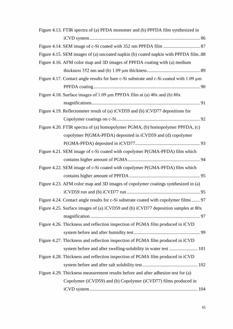
Table 1.1. Type of EO systems and Applications
(Source: Campana 1993, Fox 1996).
Applications
Passive EO
Systems
Starting-Sensor Systems
Commercial and military applications;
tracking
automatic identification
moving target demonstration
recognition
Infrared Line Scanning (IRLS)
Systems
recognition of the check points
autonomous homing vehicles
guidance
Forward-Looking Infrared (FLIR)
Systems
night vision by using thermographic
camera
search and rescue operations
target acquisition in military and civil
aircraft
Infrared Search and Track (IRST)
Systems
Military applications;
determination and tracking of
infrared emitting objects
tracking of multivarious targets
warning systems for air vehicles
Active EO
Systems
Laser Radar
target tracking
target identification and recognition
imaging
detection of the small objects
vibration sensing
wind shear identification
Millimeter-Wave Radar
missile guidance
fire control for ground targets
tracking for airborne targets
automotive braking systems
automotive warning systems
Laser Rangefinders
Military and commercial applications;
long range tracking
tank fire control
cloud height measurement
missile command guidance
Fiber Optic Systems
telecommunication applications
transferring of data and information
endoscopic imaging applications
transportation systems
distribution of video and data services
Electro-Optical systems used in military and civil aviation applications such as
night vision systems, remote sensing and sighting devices usually include prisms, lenses
and mirrors as optical surfaces, and these surfaces are made of many different inorganic
and organic materials. Such materials include sapphire, calcite (CaCO3), silica, barium
3
fluoride (BaF2), lithium fluoride (LiF), germanium (Ge), calcium fluoride (CaF2),
magnesium fluoride (MgF2), quartz (SiO2), F2, Urea, N-BK7, Teflon (PTFE),
poly(methyl methacrylate) (PMMA), poly(styrene) (PS), zinc selenide (ZnSe), Ohara
FPL glass (especially S-FPL51 and S-FPL53 equivalent), other dielectric
(inorganic/organic) materials, and certain metals such as Al, Ag etc. (Nalwa and Miyata
1996, Wakaki 2012).
Electro-Optical systems are exposed to quite harsh and unstable operating
conditions like sudden changes in temperature, humidity, dust, fog, physical shock,
vibration, radiation, etc. If their optical surfaces are damaged because of these conditions,
their repair usually is not possible. Scratches, cracks, stains, roughness and corrosion
occurs due to the physical and chemical factors thus generally these usually very
expensive optical surfaces are removed and replaced with new pieces. These are also
financially negative factors. Therefore, it is necessary to develop a special coating for
these surfaces. In addition, these optical surfaces should be protected against all corrosive
vapors (jet fuel, diesel, gasoline etc.) and liquid spills.
The main goal of this study is to produce self-cleaning and super-hydrophobic
polymeric or hybrid thin films for protection of optical surfaces of EO systems from
physical and chemical elements without any measurable decrease in optical performance.
1.2. Optical Coating Technology and Applications
Nowadays, the complexity of the optical systems are increasing quickly therefore
it has become even more important to protect these systems from elements and to make
them more durable. As a result, surfaces of the optical components used in many areas
are now coated with thin films and the optical properties of the components can be
modified with use of inorganic coatings.
Optical technology is continuously evolving hence it is needed to develop
available coating techniques or find novel and distinct ones to keep up with the new
application requirements. In addition, the film material selection is also significant
because the film materials that are coated to the surface of the optical components with
the different techniques should have to provide sufficient environmental and mechanical
protection. Materials used in the optical systems such as transparent materials which have
4
appropriate refractive indices and also high reflective opaque materials were limited in
terms of diversity in the past.
However, with the advancements in materials science and optical coating
technology a variety of materials have found use in distinct wavelength regions according
to the operating conditions of the optical systems. In the next section, the types of the
optical materials and their properties will be discussed.
1.2.1. Optical Materials and Their Properties
Various optical materials have evolved depending on the different application
areas and operating conditions of the optical systems. Therefore, many sort of materials
having a lot diverse optical properties came up and continues to emerge.
Optical property of a material can be defined as response of materials or their
interactions taken place when they are exposed to the electromagnetic radiation,
especially to visible light.
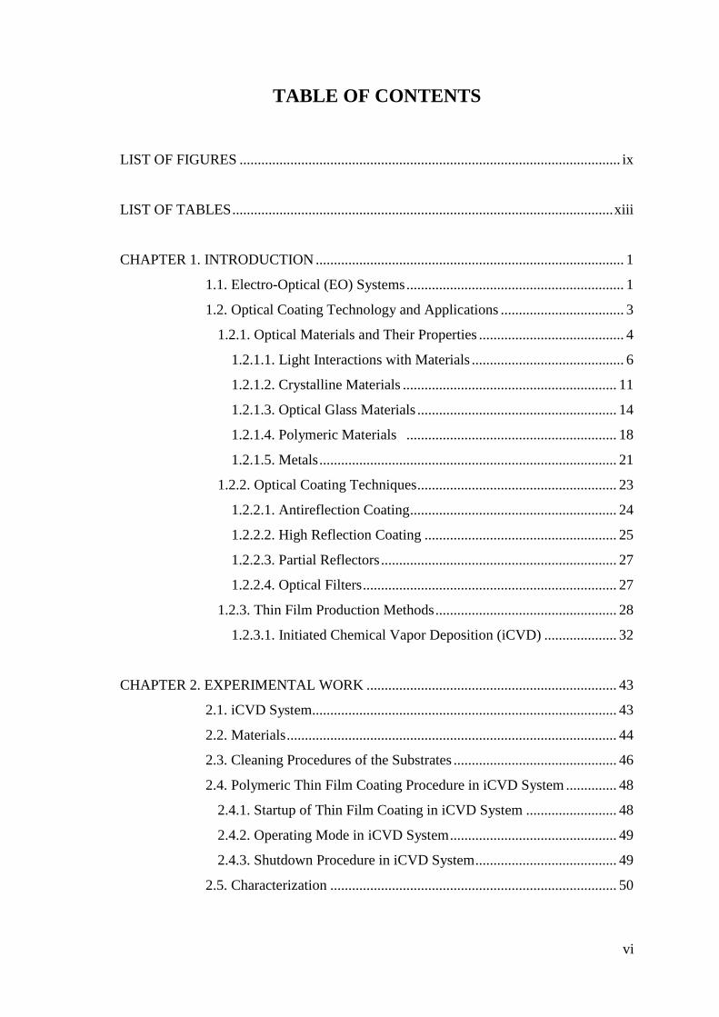
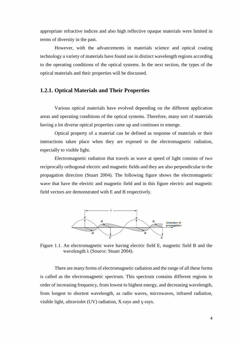
Electromagnetic radiation that travels as wave at speed of light consists of two
reciprocally orthogonal electric and magnetic fields and they are also perpendicular to the
propagation direction (Stuart 2004). The following figure shows the electromagnetic
wave that have the electric and magnetic field and in this figure electric and magnetic
field vectors are demonstrated with E and B respectively.
Figure 1.1. An electromagnetic wave having electric field E, magnetic field B and the
wavelength λ (Source: Stuart 2004).
There are many forms of electromagnetic radiation and the range of all these forms
is called as the electromagnetic spectrum. This spectrum contains different regions in
order of increasing frequency, from lowest to highest energy, and decreasing wavelength,
from longest to shortest wavelength, as radio waves, microwaves, infrared radiation,
visible light, ultraviolet (UV) radiation, X-rays and ɣ-rays.
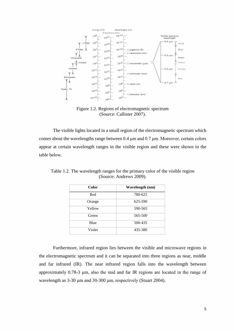
5
Figure 1.2. Regions of electromagnetic spectrum
(Source: Callister 2007).
The visible lights located in a small region of the electromagnetic spectrum which
comes about the wavelengths range between 0.4 μm and 0.7 μm. Moreover, certain colors
appear at certain wavelength ranges in the visible region and these were shown in the
table below.
Table 1.2. The wavelength ranges for the primary color of the visible region
(Source: Andrews 2009).
Color Wavelength (nm)
Red 780-625
Orange 625-590
Yellow 590-565
Green 565-500
Blue 500-435
Violet 435-380
Furthermore, infrared region lies between the visible and microwave regions in
the electromagnetic spectrum and it can be separated into three regions as near, middle
and far infrared (IR). The near infrared region falls into the wavelength between
approximately 0.78-3 μm, also the mid and far IR regions are located in the range of
wavelength as 3-30 μm and 30-300 μm, respectively (Stuart 2004).
6
1.2.1.1. Light Interactions with Materials
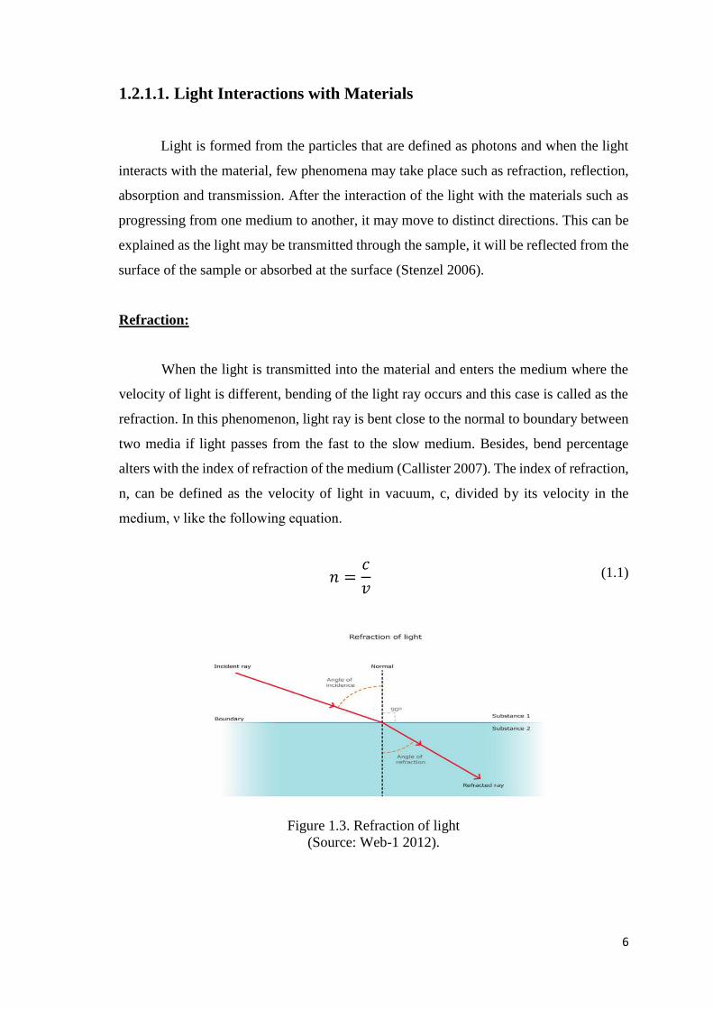
Light is formed from the particles that are defined as photons and when the light
interacts with the material, few phenomena may take place such as refraction, reflection,
absorption and transmission. After the interaction of the light with the materials such as
progressing from one medium to another, it may move to distinct directions. This can be
explained as the light may be transmitted through the sample, it will be reflected from the
surface of the sample or absorbed at the surface (Stenzel 2006).
Refraction:
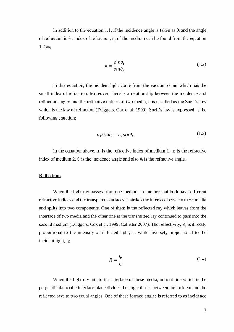
When the light is transmitted into the material and enters the medium where the
velocity of light is different, bending of the light ray occurs and this case is called as the
refraction. In this phenomenon, light ray is bent close to the normal to boundary between
two media if light passes from the fast to the slow medium. Besides, bend percentage
alters with the index of refraction of the medium (Callister 2007). The index of refraction,
n, can be defined as the velocity of light in vacuum, c, divided by its velocity in the
medium, ν like the following equation.
𝑛 =𝑐
𝑣
Figure 1.3. Refraction of light
(Source: Web-1 2012).
(1.1)
7
In addition to the equation 1.1, if the incidence angle is taken as θi and the angle
of refraction is θr, index of refraction, n, of the medium can be found from the equation
1.2 as;
𝑛 =𝑠𝑖𝑛𝜃𝑖
𝑠𝑖𝑛𝜃𝑟
In this equation, the incident light come from the vacuum or air which has the
small index of refraction. Moreover, there is a relationship between the incidence and
refraction angles and the refractive indices of two media, this is called as the Snell’s law
which is the law of refraction (Driggers, Cox et al. 1999). Snell’s law is expressed as the
following equation;
𝑛1𝑠𝑖𝑛𝜃𝑖 = 𝑛2𝑠𝑖𝑛𝜃𝑟
In the equation above, n1 is the refractive index of medium 1, n2 is the refractive
index of medium 2, θi is the incidence angle and also θr is the refractive angle.
Reflection:
When the light ray passes from one medium to another that both have different
refractive indices and the transparent surfaces, it strikes the interface between these media
and splits into two components. One of them is the reflected ray which leaves from the
interface of two media and the other one is the transmitted ray continued to pass into the
second medium (Driggers, Cox et al. 1999, Callister 2007). The reflectivity, R, is directly
proportional to the intensity of reflected light, Ir, while inversely proportional to the
incident light, Ii;
𝑅 =𝐼𝑟
𝐼𝑖
When the light ray hits to the interface of these media, normal line which is the
perpendicular to the interface plane divides the angle that is between the incident and the
reflected rays to two equal angles. One of these formed angles is referred to as incidence
(1.2)
(1.3)
(1.4) (1.4)
(1.3)
8
angle because it is placed between the incident light and the normal line, and the other
angle is called as the reflection angle and it is located between the normal line and the
reflected ray. This case is called as the law of reflection because this law states that the
angle of incidence and reflection equals to each other when a light ray reflects from
interface of two media (Driggers, Cox et al. 1999).
Absorption:
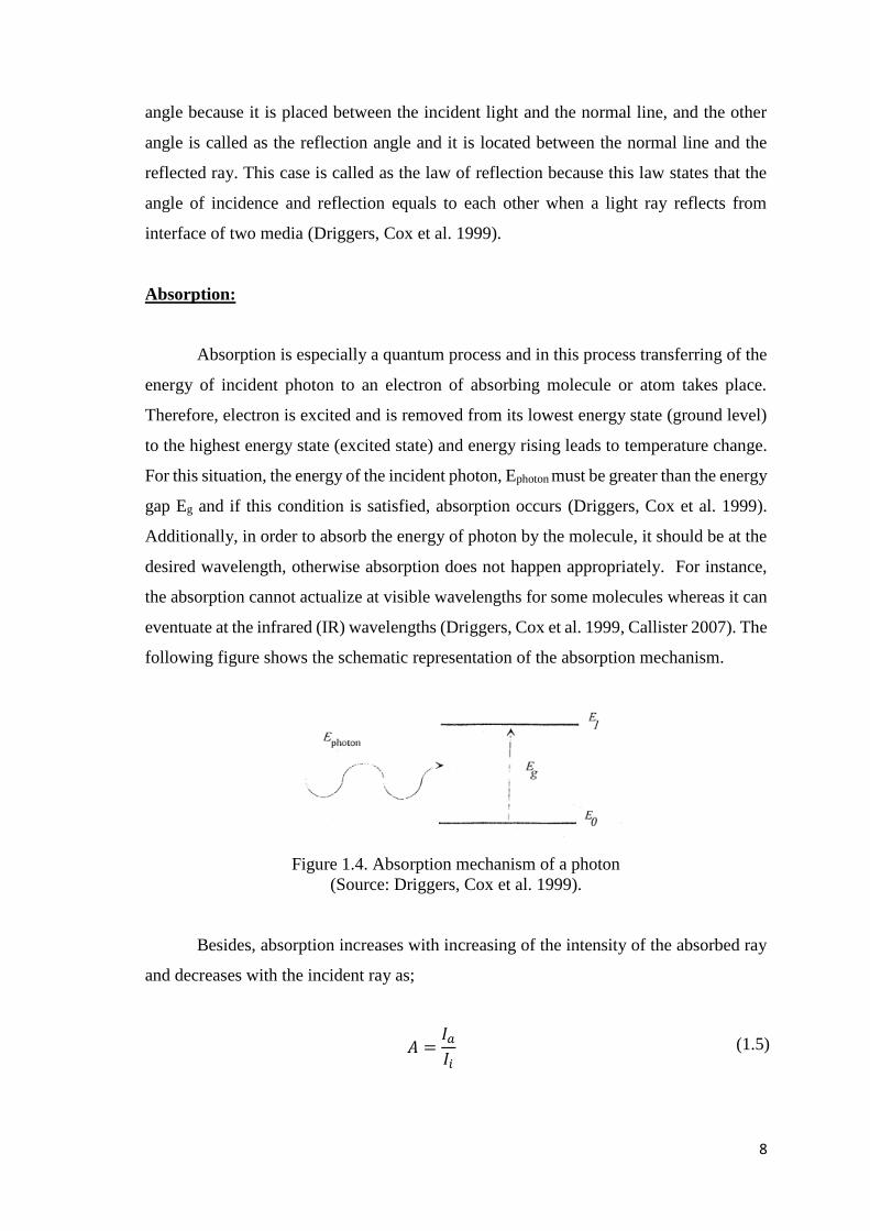
Absorption is especially a quantum process and in this process transferring of the
energy of incident photon to an electron of absorbing molecule or atom takes place.
Therefore, electron is excited and is removed from its lowest energy state (ground level)
to the highest energy state (excited state) and energy rising leads to temperature change.
For this situation, the energy of the incident photon, Ephoton must be greater than the energy
gap Eg and if this condition is satisfied, absorption occurs (Driggers, Cox et al. 1999).
Additionally, in order to absorb the energy of photon by the molecule, it should be at the
desired wavelength, otherwise absorption does not happen appropriately. For instance,
the absorption cannot actualize at visible wavelengths for some molecules whereas it can
eventuate at the infrared (IR) wavelengths (Driggers, Cox et al. 1999, Callister 2007). The
following figure shows the schematic representation of the absorption mechanism.
Figure 1.4. Absorption mechanism of a photon
(Source: Driggers, Cox et al. 1999).
Besides, absorption increases with increasing of the intensity of the absorbed ray
and decreases with the incident ray as;
𝐴 =𝐼𝑎
𝐼𝑖
(1.5) (1.5)
9
Transmission:
Transmission is realized when the incident light, which is not reflected or
absorbed, passes through the material. There are three types of this process as direct,
diffuse and selective. In the direct transmission, incident light goes through the material
without any direction change. Besides, diffuse transmission occurs when the incident
light pass through the material and light is not only move in one direction, is also
dispersed in distinct directions. In addition to these processes, selective transmission takes
place when the light progresses through a colored transparent material. In this process,
some of the incident light are absorbed by the material and some parts transmitted
according to the colors at certain wavelengths (Web-2 , Callister 2007).
Furthermore, transmittance is directly related with the intensity of transmitted
light, It, whereas there is an inverse ratio between transmittance and the incident light, Ii
as;
𝑇 =𝐼𝑡
𝐼𝑖
The intensity of the incident light, Ii, ray equals to the sum of the intensities of the
reflected, absorbed and transmitted lights as;
𝐼𝑖 = 𝐼𝑟 + 𝐼𝑎 + 𝐼𝑡
Besides of this equation, the sum of the reflectivity, R, absorptivity, A, and
transmittance, T, should be equal to the unity because all the incident light that impinges
to the surface of the material reflected, transmitted or absorbed (Callister 2007).
Fresnel’s Equations:
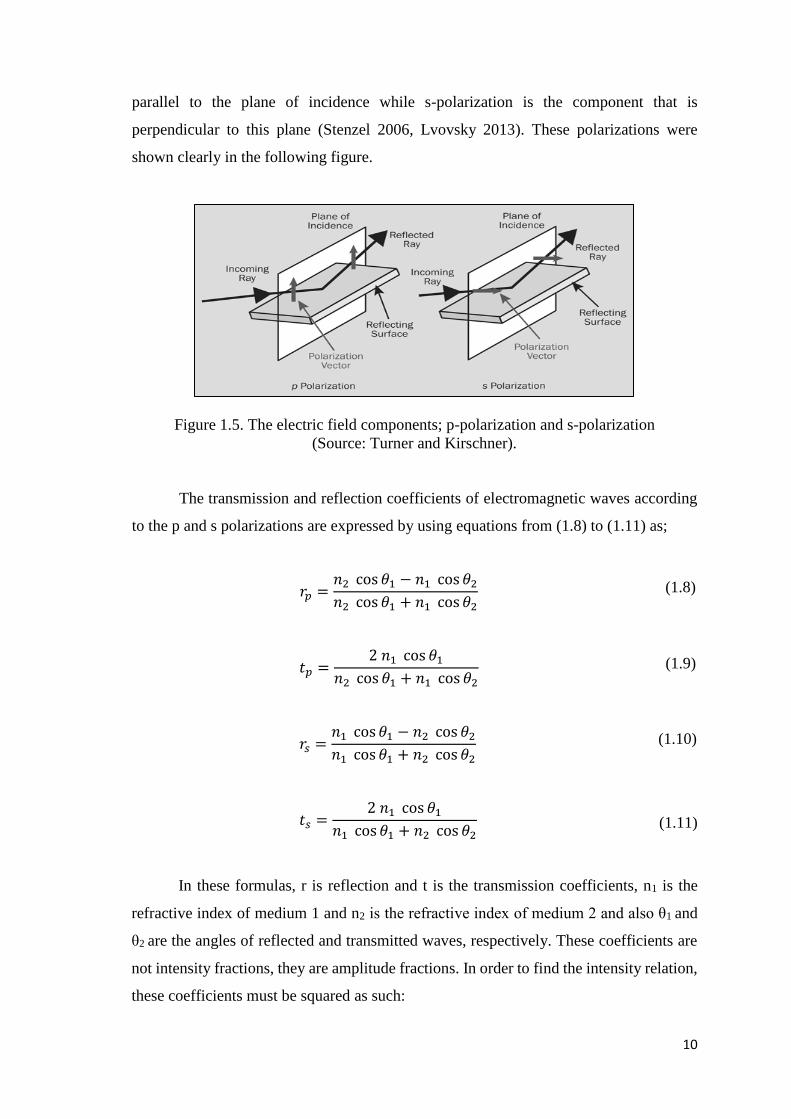
The transmission and reflection coefficients of the electromagnetic wave at
surfaces and interfaces can be identified by using the Fresnel’s equations. When the
incident light comes through the surface of the material and enters the interface of distinct
media, two different polarization components occur from field incident at the interface as
“p” and “s” polarizations. P-polarization can be defined as the electric field component
(1.6)
(1.7)
10
parallel to the plane of incidence while s-polarization is the component that is
perpendicular to this plane (Stenzel 2006, Lvovsky 2013). These polarizations were
shown clearly in the following figure.
Figure 1.5. The electric field components; p-polarization and s-polarization
(Source: Turner and Kirschner).
The transmission and reflection coefficients of electromagnetic waves according
to the p and s polarizations are expressed by using equations from (1.8) to (1.11) as;
𝑟𝑝 =𝑛2 cos 𝜃1 − 𝑛1 cos 𝜃2
𝑛2 cos 𝜃1 + 𝑛1 cos 𝜃2
𝑡𝑝 =2 𝑛1 cos 𝜃1
𝑛2 cos 𝜃1 + 𝑛1 cos 𝜃2
𝑟𝑠 =𝑛1 cos 𝜃1 − 𝑛2 cos 𝜃2
𝑛1 cos 𝜃1 + 𝑛2 cos 𝜃2
𝑡𝑠 =2 𝑛1 cos 𝜃1
𝑛1 cos 𝜃1 + 𝑛2 cos 𝜃2
In these formulas, r is reflection and t is the transmission coefficients, n1 is the
refractive index of medium 1 and n2 is the refractive index of medium 2 and also θ1 and
θ2 are the angles of reflected and transmitted waves, respectively. These coefficients are
not intensity fractions, they are amplitude fractions. In order to find the intensity relation,
these coefficients must be squared as such:
(1.8)
(1.9)
(1.10)
(1.11)
11
𝑅𝑝 = |𝑟𝑝|2 , 𝑇𝑝 = |𝑡𝑝|
2
𝑅𝑠 = |𝑟𝑠|2 , 𝑇𝑠 = |𝑡𝑠|2
Interaction of light with optical materials and how optical properties of materials
change in terms of these interactions have been explained above. The materials that have
different optical features as a result of light interactions also have diverse electrical,
thermal and mechanical properties. Therefore, these materials can be used suitably in
distinct application areas of the electro-optical systems. The optical materials can be
grouped under four main headings as crystalline materials, glasses, polymeric materials
and metals. In the next sections, these materials and their physical, optical, mechanical
and thermal properties will be explained.
1.2.1.2. Crystalline Materials
The optical crystalline materials are usually employed at the wavelengths from
100nm to 100μm in the electromagnetic spectrum and they are mostly transparent from
the ultraviolet (UV) to infrared region despite of seeming as opaque in only small parts
of this range. The optical crystals can be divided into two main groups as isotropic and
anisotropic crystals (Weber 2002).
In isotropic crystals, light exhibits the same behavior regardless of its movement
direction in the medium thus their properties do not alter in any directions. However, in
anisotropic crystals, light ray acts distinctly different in different directions through the
medium since material properties depend on geometries of crystals (Weber 2002).
Besides, the anisotropic crystals can be classified as uniaxial and biaxial crystals. The
uniaxial crystals, which possess only one optic axis, contain three different crystal
geometries as tetragonal, hexagonal and trigonal. In addition to this, there are two specific
refractive indices as ω and ε. Moreover, the biaxial crystals are called with this name due
to having two optic axes and orthorhombic, monoclinic and triclinic crystal systems fall
into biaxial category. Unlike the uniaxial crystals, this crystal type has three unique
refractive indices according to the increasing value as α, β and γ, respectively (Web-3 ,
Weber 2002).
(1.12)
12
Table 1.3. Crystal Systems
(Source: Callister 2007).
Isotropic Anisotropic Crystals
Crystals
Uniaxial Biaxial
Crystal
System Cubic Tetragonal Hexagonal Trigonal Orthorhombic Monoclinic Triclinic
Unit Cell
Geometry
If the optical implementation areas are examined according to the crystal systems,
it can be found that anisotropic crystals mostly utilized in optical wave plates and
polarizers while the usage areas of the isotropic crystals are lenses and windows.
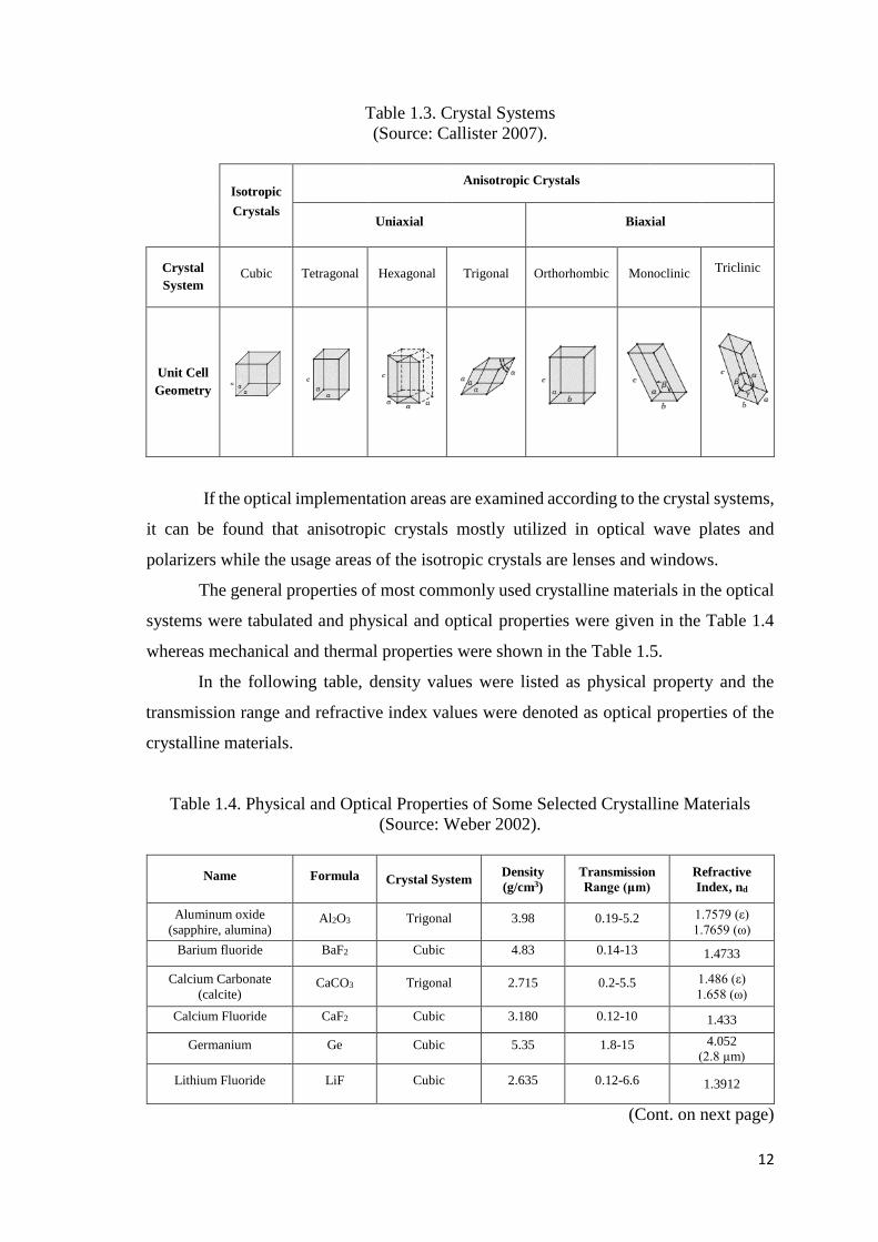
The general properties of most commonly used crystalline materials in the optical
systems were tabulated and physical and optical properties were given in the Table 1.4
whereas mechanical and thermal properties were shown in the Table 1.5.
In the following table, density values were listed as physical property and the
transmission range and refractive index values were denoted as optical properties of the
crystalline materials.
Table 1.4. Physical and Optical Properties of Some Selected Crystalline Materials
(Source: Weber 2002).
Name Formula Crystal System Density
(g/cm3)
Transmission
Range (μm)
Refractive
Index, nd
Aluminum oxide
(sapphire, alumina) Al2O3 Trigonal 3.98 0.19-5.2 1.7579 (ε)
1.7659 (ω)
Barium fluoride BaF2 Cubic 4.83 0.14-13 1.4733
Calcium Carbonate
(calcite) CaCO3 Trigonal 2.715 0.2-5.5 1.486 (ε)
1.658 (ω)
Calcium Fluoride CaF2 Cubic 3.180 0.12-10 1.433
Germanium Ge Cubic 5.35 1.8-15 4.052
(2.8 µm)
Lithium Fluoride LiF Cubic 2.635 0.12-6.6 1.3912
(Cont. on next page)
13
Table 1.4. (Cont.)
Name Formula Crystal System Density
(g/cm3)
Transmission
Range (μm)
Refractive
Index, nd
Lithium Niobate LiNbO3 Trigonal 4.644 0.35-5.0 2.156 (ε)
2.232 (ω)
Magnesium Fluoride MgF2 Tetragonal 3.18 0.13-7.7 1.3886 (ε)
1.3768 (ω)
Silicon Si Cubic 2.33 1.1-6.5 3.4777
(1.55 µm)
Silicon Dioxide
(α-quartz) SiO2 Trigonal 2.65 0.16-4.0 1.56 (ε)
1.55 (ω)
Zinc Selenide ZnSe Cubic 5.42 0.5-20 2.5907
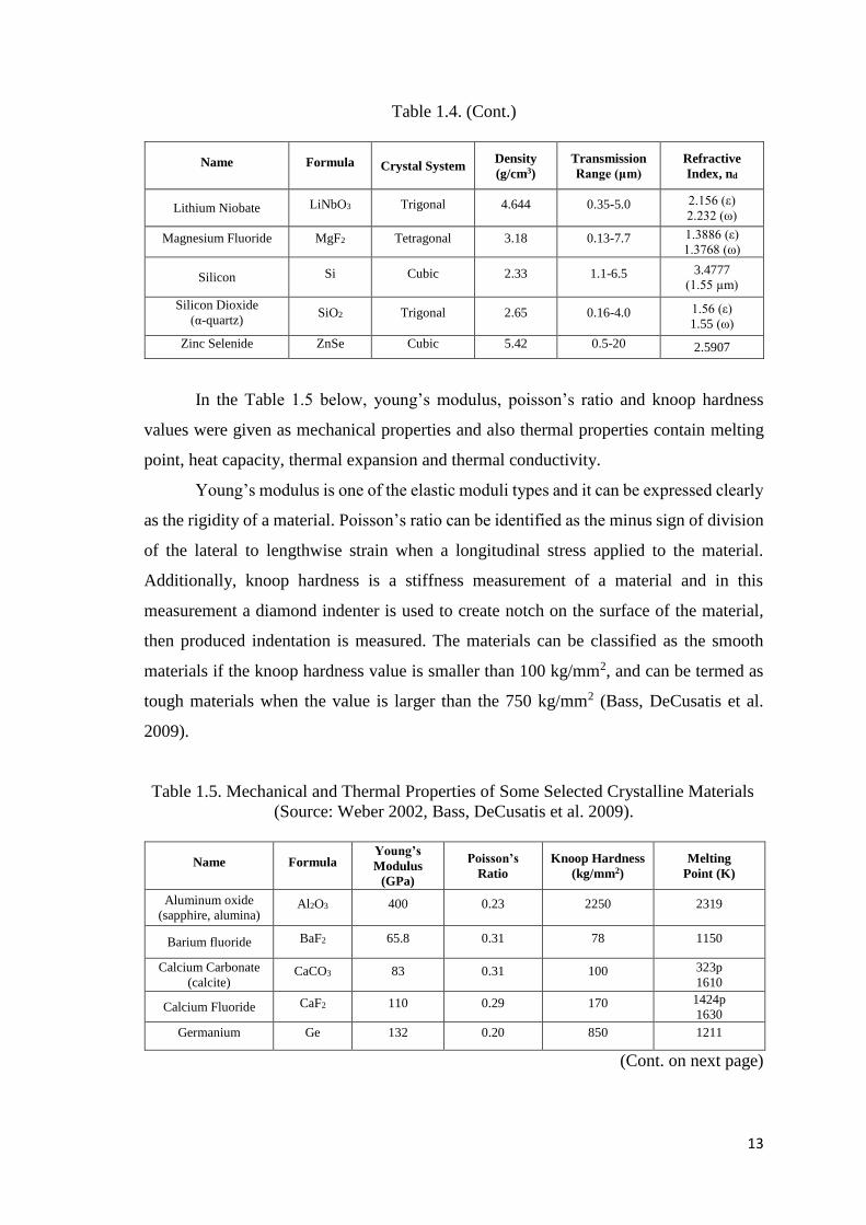
In the Table 1.5 below, young’s modulus, poisson’s ratio and knoop hardness
values were given as mechanical properties and also thermal properties contain melting
point, heat capacity, thermal expansion and thermal conductivity.
Young’s modulus is one of the elastic moduli types and it can be expressed clearly
as the rigidity of a material. Poisson’s ratio can be identified as the minus sign of division
of the lateral to lengthwise strain when a longitudinal stress applied to the material.
Additionally, knoop hardness is a stiffness measurement of a material and in this
measurement a diamond indenter is used to create notch on the surface of the material,
then produced indentation is measured. The materials can be classified as the smooth
materials if the knoop hardness value is smaller than 100 kg/mm2, and can be termed as
tough materials when the value is larger than the 750 kg/mm2 (Bass, DeCusatis et al.
2009).
Table 1.5. Mechanical and Thermal Properties of Some Selected Crystalline Materials
(Source: Weber 2002, Bass, DeCusatis et al. 2009).
Name Formula Young’s
Modulus
(GPa)
Poisson’s
Ratio
Knoop Hardness
(kg/mm2)
Melting
Point (K)
Aluminum oxide
(sapphire, alumina) Al2O3 400 0.23 2250 2319
Barium fluoride BaF2 65.8 0.31 78 1150
Calcium Carbonate
(calcite) CaCO3 83 0.31 100 323p
1610
Calcium Fluoride CaF2 110 0.29 170 1424p
1630
Germanium Ge 132 0.20 850 1211
(Cont. on next page)
14
Table 1.5. (Cont.)
Name Formula Young’s
Modulus
(GPa)
Poisson’s
Ratio
Knoop Hardness
(kg/mm2)
Melting
Point (K)
Lithium Fluoride LiF 110 0.22 115 1115
Lithium Niobate LiNbO3 170 0.25 630 1523
Magnesium Fluoride MgF2 137 0.26 500 1536
Silicon Si 162 0.22 1150 1680
Silicon Dioxide
(α-quartz) SiO2 95 0.08 740 845p
Zinc Selenide ZnSe 75.4 0.30 115 1790
p-phase change
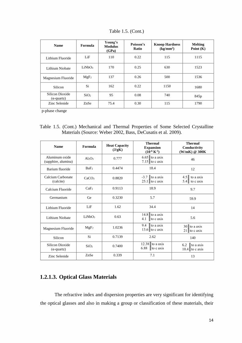
Table 1.5. (Cont.) Mechanical and Thermal Properties of Some Selected Crystalline
Materials (Source: Weber 2002, Bass, DeCusatis et al. 2009).
Name Formula Heat Capacity
(J/gK)
Thermal
Expansion
(10-6 K-1)
Thermal
Conductivity
(W/mK) @ 300K
Aluminum oxide
(sapphire, alumina) Al2O3 0.777 6.65║to a axis
7.15║to c axis 46
Barium fluoride BaF2 0.4474 18.4 12
Calcium Carbonate
(calcite) CaCO3 0.8820 -3.7 ║to a axis
25.1║to c axis
4.5║ to a axis
5.4║ to c axis
Calcium Fluoride CaF2 0.9113 18.9 9.7
Germanium Ge 0.3230 5.7 59.9
Lithium Fluoride LiF 1.62 34.4 14
Lithium Niobate LiNbO3 0.63 14.8║to a axis
4.1 ║to c axis 5.6
Magnesium Fluoride MgF2 1.0236 9.4 ║to a axis
13.6║to c axis 30║to a axis
21║to c axis
Silicon Si 0.7139 2.62 140
Silicon Dioxide
(α-quartz) SiO2 0.7400
12.38║to a axis
6.88 ║to c axis 6.2 ║to a axis
10.4║to c axis
Zinc Selenide ZnSe 0.339 7.1 13
1.2.1.3. Optical Glass Materials
The refractive index and dispersion properties are very significant for identifying
the optical glasses and also in making a group or classification of these materials, their
15
components, which constitute them, play substantial roles. The refractive index that was
explained in detail in the refraction part of the light interactions with materials section of
this study can be described briefly as a bending measure of a light. It occurs when a light
ray goes from one medium to another where is the velocity of light different. Moreover,
dispersion property can be expressed with the abbe number, vd, and it is identified as
dispersion measure of a light (Weber 2002). Abbe number can be found by using the
following equation;
𝑣𝑑 =𝑛𝑑 − 1
𝑛𝐹 − 𝑛𝐶
In this equation, nd, nF and nC are the refractive indices at the specific wavelengths
of the Fraunhofer’s lines which are the absorption lines seen in the spectrum owing to the
absorption of the light ray. Besides, the letter d, F and C represent the d-, F- and C-spectral
lines at wavelengths of 589.3, 486.1 and 656.3 nm, respectively (Weber 2002).
There are many types of the optical glasses and they are usually encoded for
universal identification. The glass materials receive the crown (K) name if their refractive
index and abbe numbers are larger than 1.60 and 50, respectively, or refractive index value
is smaller than 1.60 but abbe number value is greater than 55. On the other hand, flint (F)
name is given to the glass materials if they have high refractive index (range from 1.45 to
2.00) and low abbe number values (vd<55). Additionally, different abbreviations are
applied to the names of the components formed the glass materials by the manufacturers
of them such as Hoya Glass Works Ltd, Schott Optical Glass Inc., Ohara Optical Glass
Inc. etc. For instance, borosilicate Crown glass is encoded as “BSC” by Hoya, “BK” by
Schott and “BSL” by Ohara Inc (Weber 2002, Bass, DeCusatis et al. 2009). Another
encoding type is “mil spec” and in this type, the glass materials are identified with the six
digit number. The first three digit of the number demonstrates the refractive index value
of related material and the other three digit displays the abbe number of the material. For
example, refractive index and the abbe number of borosilicate crown glass are 1.517 and
64.17, respectively. When this glass type is encoded according to the mil spec, in the
refractive index value the next three digits after the number “1” is taken and in the abbe
number value, decimal point is ignored. Therefore, the coding for borosilicate crown glass
is made as 517-642 (Weber 2002).
(1.13)
16
The following tables shows the optical, thermal and mechanical properties of the
common glass materials used in the optical systems. In Table 1.6, encoding types and
densities of the glass materials are given, optical and mechanical properties are shown in
Table 1.7 and also thermal properties of the materials are displayed in Table 1.8.
Table 1.6. Encoding Types and Densities of Some Selected Glasses
(Source: Weber 2002, Bass, DeCusatis et al. 2009).
Encoding Types
Glass Type Schott Type Ohara Type Hoya Type Corning Type
Borosilicate
Crown
N-BK 7
(517-642)
ρ=2.51
S-BSL7
(516-614)
ρ=2.52
BSC7
(517-642)
ρ=2.52
B16-64
Fluoro Crown
N-FK 5
(487-704)
ρ=2.45
S-FSL5
(487-702)
ρ=2.46
FC5
(487-704)
ρ=2.45
A87-70
Phosphate
Crown
N-PK52A
(497-816)
ρ=3.70
S-FPL51
(497-816)
ρ=3.62
FCD1
(497-816)
ρ=3.70
-
Barium Crown
N-BaK4
(569-560)
ρ=3.05
S-BAL14
(569-563)
ρ=2.89
BAC4
(569-560)
ρ=2.85
B69-56
Crown
N-K5
(522-595)
ρ=2.59
S-NSL5
(522-598)
ρ=2.49
- B23-59
Fluoro Flint
TiF1
(511-510)
ρ=2.48
S-FTM16
(593-353)
ρ=2.64
FF5
(593-354)
ρ=2.64
-
Barium Flint
N-BaF10
(670-471)
ρ=3.75
S-BAH10
(670-473)
ρ=3.48
BAF10
(670-472)
ρ=3.61
-
Flint
N-F2
(620-364)
ρ=2.65
S-TIM1
(626-357)
ρ=2.71
E-F2
(620-363)
ρ=2.67
C20-36
Antimony Flint
KzFN1
(551-496)
ρ=2.71
-
SbF1
(551-495)
ρ=2.72
-
Density, ρ (g/cm3) @ 25oC
(Cont. on next page)
17
Table 1.6. (Cont.)
Unique Glasses
Fused Silica
(UV)
Lithosil-Q
(458-678)
ρ=2.20
- - -
Pyrex - - - (474-660)
ρ=2.23
CORTRAN
9754 - - -
(660-465)
ρ=3.581
Density, ρ (g/cm3) @ 25oC
Table 1.7. Optical and Mechanical Properties of Some Selected Glasses
(Source: Weber 2002, Bass, DeCusatis et al. 2009).
Glass Type Refractive
Index, nd
Abbe
Number, vd
Young’s Modulus
(GPa) Poisson’s Ratio
Knoop
Hardness
(kg/mm2)
BK 7 1.517 64.17 81 0.206 610
FK 5 1.487 70.41 62 0.232 520
PK52A 1.497 81.60 71 0.298 355
BaK 4 1.569 56.0 77 0.24 550
K 5 1.522 59.48 71 0.224 530
TiF1 1.511 51.01 58 0.263 440
BaF10 1.670 47.11 89 0.271 620
F 2 1.620 36.37 82 0.228 600
KzFN1 1.551 49.64 60 0.276 500
Fused Silica
(UV) 1.458 67.70 72.6 0.164 635
Pyrex 1.474 66.0 62.8 0.200 418
CORTRAN
9754 1.660 46.5 84.1 0.290 560
18
Table 1.8. Thermal Properties of Some Selected Glasses
(Source: Weber 2002, Bass, DeCusatis et al. 2009).
Glass Type
Heat
Capacity
(J/gK)
Thermal
Expansion
(10-6 K-1)
Thermal
Conductivity
(W/mK) @ 300K
BK 7 0.858 7.1 1.114
FK 5 0.808 9.2 0.925
PK52A 0.67 13.01 0.73
BaK 4 0.680 6.99 0.88
K 5 0.783 8.2 0.95
TiF1 0.842 10.3 0.773
BaF10 0.56 6.18 0.78
F 2 0.81 7.84 1.05
KzFN1 - 7.5 -
Fused Silica
(UV) 0.746 0.51 1.38
Pyrex 1.05 3.25 1.13
CORTRAN
9754 0.54 6.2 0.81
1.2.1.4. Polymeric Materials
The glass materials possess very significant optical properties and are used
efficiently in the optical systems. In addition to glasses some plastic materials are also
utilized suitably in these systems. Although they show some shortcomings in terms of the
main features compared with glass like having low refractive indices, they may have
better features than many other glass properties (Bass, DeCusatis et al. 2009). For
instances, plastic materials are much lighter than the optical glass materials and this
property makes them more valuable in the applications which the weight is a significant
parameter. Besides, the impact resistance is much better for plastic materials than the
glasses that have more fragile structures and this property is required particularly in the
military applications and is also desired in many other EO systems. Moreover, physical
properties of the plastic materials make them much versatile for the optical and
mechanical design requirements because they have advantages in terms of improvement
or reconstruction of the optical components or the systems that are not easy and unlikely
with glass materials (Bass, DeCusatis et al. 2009).
19
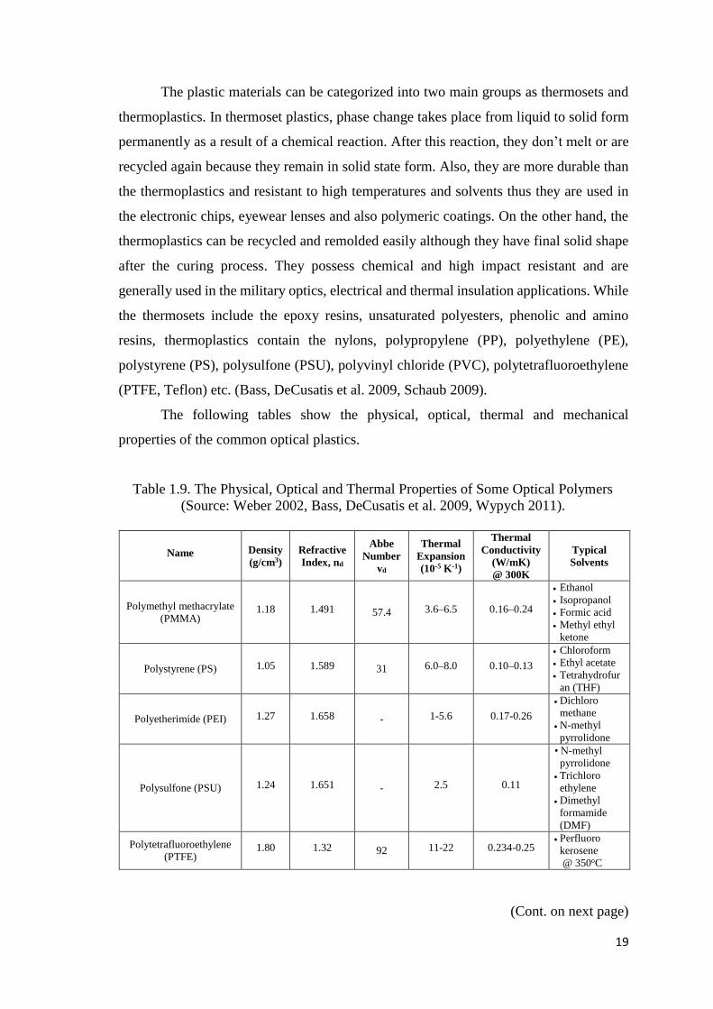
The plastic materials can be categorized into two main groups as thermosets and
thermoplastics. In thermoset plastics, phase change takes place from liquid to solid form
permanently as a result of a chemical reaction. After this reaction, they don’t melt or are
recycled again because they remain in solid state form. Also, they are more durable than
the thermoplastics and resistant to high temperatures and solvents thus they are used in
the electronic chips, eyewear lenses and also polymeric coatings. On the other hand, the
thermoplastics can be recycled and remolded easily although they have final solid shape
after the curing process. They possess chemical and high impact resistant and are
generally used in the military optics, electrical and thermal insulation applications. While
the thermosets include the epoxy resins, unsaturated polyesters, phenolic and amino
resins, thermoplastics contain the nylons, polypropylene (PP), polyethylene (PE),
polystyrene (PS), polysulfone (PSU), polyvinyl chloride (PVC), polytetrafluoroethylene
(PTFE, Teflon) etc. (Bass, DeCusatis et al. 2009, Schaub 2009).
The following tables show the physical, optical, thermal and mechanical
properties of the common optical plastics.
Table 1.9. The Physical, Optical and Thermal Properties of Some Optical Polymers
(Source: Weber 2002, Bass, DeCusatis et al. 2009, Wypych 2011).
Name Density
(g/cm3)
Refractive
Index, nd
Abbe
Number
vd
Thermal
Expansion
(10-5 K-1)
Thermal
Conductivity
(W/mK)
@ 300K
Typical
Solvents
Polymethyl methacrylate
(PMMA) 1.18 1.491 57.4 3.6–6.5 0.16–0.24
Ethanol
Isopropanol
Formic acid
Methyl ethyl
ketone
Polystyrene (PS) 1.05 1.589 31 6.0–8.0 0.10–0.13
Chloroform
Ethyl acetate
Tetrahydrofur
an (THF)
Polyetherimide (PEI) 1.27 1.658 - 1-5.6 0.17-0.26
Dichloro
methane
N-methyl
pyrrolidone
Polysulfone (PSU) 1.24 1.651 - 2.5 0.11
• N-methyl
pyrrolidone
Trichloro
ethylene
Dimethyl
formamide
(DMF)
Polytetrafluoroethylene
(PTFE) 1.80 1.32 92 11-22 0.234-0.25
Perfluoro
kerosene
@ 350oC
(Cont. on next page)
20
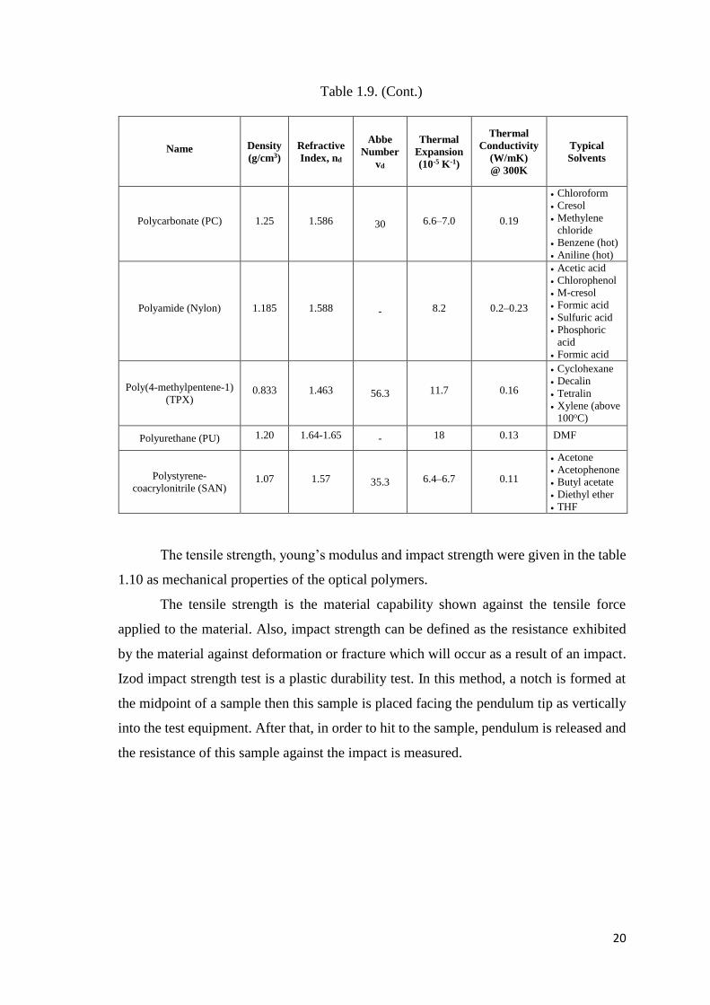
Table 1.9. (Cont.)
Name Density
(g/cm3)
Refractive
Index, nd
Abbe
Number
vd
Thermal
Expansion
(10-5 K-1)
Thermal
Conductivity
(W/mK)
@ 300K
Typical
Solvents
Polycarbonate (PC) 1.25 1.586 30 6.6–7.0 0.19
Chloroform
Cresol
Methylene
chloride
Benzene (hot)
Aniline (hot)
Polyamide (Nylon) 1.185 1.588 - 8.2 0.2–0.23
Acetic acid
Chlorophenol
M-cresol
Formic acid
Sulfuric acid
Phosphoric
acid
Formic acid
Poly(4-methylpentene-1)
(TPX) 0.833 1.463 56.3 11.7 0.16
Cyclohexane
Decalin
Tetralin
Xylene (above
100oC)
Polyurethane (PU) 1.20 1.64-1.65 - 18 0.13 DMF
Polystyrene-
coacrylonitrile (SAN) 1.07 1.57 35.3 6.4–6.7 0.11
Acetone
Acetophenone
Butyl acetate
Diethyl ether
THF
The tensile strength, young’s modulus and impact strength were given in the table
1.10 as mechanical properties of the optical polymers.
The tensile strength is the material capability shown against the tensile force
applied to the material. Also, impact strength can be defined as the resistance exhibited
by the material against deformation or fracture which will occur as a result of an impact.
Izod impact strength test is a plastic durability test. In this method, a notch is formed at
the midpoint of a sample then this sample is placed facing the pendulum tip as vertically
into the test equipment. After that, in order to hit to the sample, pendulum is released and
the resistance of this sample against the impact is measured.
21
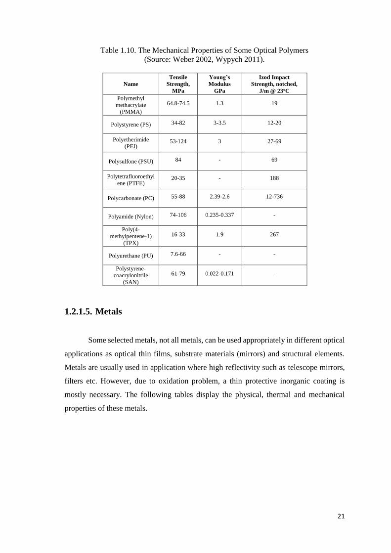
Table 1.10. The Mechanical Properties of Some Optical Polymers
(Source: Weber 2002, Wypych 2011).
Name
Tensile
Strength,
MPa
Young’s
Modulus
GPa
Izod Impact
Strength, notched,
J/m @ 23oC
Polymethyl
methacrylate
(PMMA)
64.8-74.5 1.3 19
Polystyrene (PS) 34-82 3-3.5 12-20
Polyetherimide
(PEI) 53-124 3 27-69
Polysulfone (PSU) 84 - 69
Polytetrafluoroethyl
ene (PTFE) 20-35 - 188
Polycarbonate (PC) 55-88 2.39-2.6 12-736
Polyamide (Nylon) 74-106 0.235-0.337 -
Poly(4-
methylpentene-1)
(TPX)
16-33 1.9 267
Polyurethane (PU) 7.6-66 - -
Polystyrene-
coacrylonitrile
(SAN)
61-79 0.022-0.171 -
1.2.1.5. Metals
Some selected metals, not all metals, can be used appropriately in different optical
applications as optical thin films, substrate materials (mirrors) and structural elements.
Metals are usually used in application where high reflectivity such as telescope mirrors,
filters etc. However, due to oxidation problem, a thin protective inorganic coating is
mostly necessary. The following tables display the physical, thermal and mechanical
properties of these metals.
22
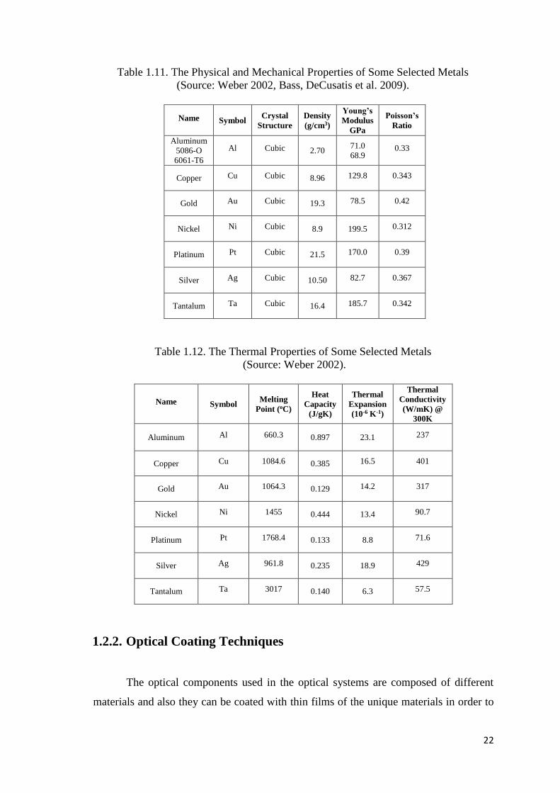
Table 1.11. The Physical and Mechanical Properties of Some Selected Metals
(Source: Weber 2002, Bass, DeCusatis et al. 2009).
Name Symbol Crystal
Structure
Density
(g/cm3)
Young’s
Modulus
GPa
Poisson’s
Ratio
Aluminum
5086-O
6061-T6
Al Cubic 2.70 71.0
68.9 0.33
Copper Cu Cubic 8.96 129.8 0.343
Gold Au Cubic 19.3 78.5 0.42
Nickel Ni Cubic 8.9 199.5 0.312
Platinum Pt Cubic 21.5 170.0 0.39
Silver Ag Cubic 10.50 82.7 0.367
Tantalum Ta Cubic 16.4 185.7 0.342
Table 1.12. The Thermal Properties of Some Selected Metals
(Source: Weber 2002).
Name Symbol Melting
Point (oC)
Heat
Capacity
(J/gK)
Thermal
Expansion
(10-6 K-1)
Thermal
Conductivity
(W/mK) @
300K
Aluminum Al 660.3 0.897 23.1 237
Copper Cu 1084.6 0.385 16.5 401
Gold Au 1064.3 0.129 14.2 317
Nickel Ni 1455 0.444 13.4 90.7
Platinum Pt 1768.4 0.133 8.8 71.6
Silver Ag 961.8 0.235 18.9 429
Tantalum Ta 3017 0.140 6.3 57.5
1.2.2. Optical Coating Techniques
The optical components used in the optical systems are composed of different
materials and also they can be coated with thin films of the unique materials in order to
23
possess some specific features that might be required by the application and operating
environment of the optical systems. Actually, these specific features are the reflection
and transmission properties and they can be easily altered and improved to achieve
desired conditions with the thin film coatings.
When the light ray goes from one medium to another which have distinct optical
properties, especially different refractive indices, some of the light is transmitted whereas
some of them is reflected. In the optical component designs, the percentages of the
transmission and the reflection of light occupy the important positions one can run into
undesirable cases due to lack of the transmitted or reflected lights.
For instance, lenses can cause some visual disorders such as ghost images that can
be defined as forming two images instead of one and they occur with the reflection of
light as a result of the failure to transmit the certain amount of light. In order to prevent
such undesired events thin film coating designs must be performed carefully before
fabrication. According to the implementation of the optical components such as optical
transmitters, reflective optics etc., coating designs are changed. In the optical transmitters
like lenses, it is required that the transmitting section of the light becomes 100 percent
while the reflection part goes to zero. However, for reflective optics like the mirrors,
100% reflection it is desired.
There are different coating techniques to meet the desired conditions explained
above as antireflection coating, high reflection coating and also coatings for partial
reflectors and optical filters. In the next sections, these coating techniques will be
described briefly.
1.2.2.1. Antireflection Coating
Antireflection (AR) coating is a commonly used coating type that is used to reduce
the reflection of light and also improve the transmission. A phase change of 180o is used
to eliminate light transmission losses in antireflection coatings of the thin films.
Light also behaves like wave, therefore it creates interference effects that can be
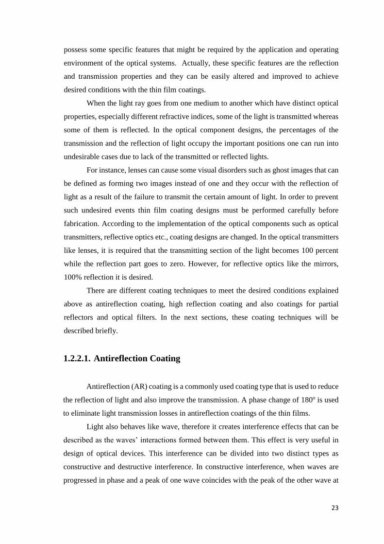
described as the waves’ interactions formed between them. This effect is very useful in
design of optical devices. This interference can be divided into two distinct types as
constructive and destructive interference. In constructive interference, when waves are
progressed in phase and a peak of one wave coincides with the peak of the other wave at
24
the same point, the resultant wave which has a magnitude equal to the sum of the
magnitude of individual waves. In destructive interference, wave interactions take place
and the resultant wave magnitude is equal to the difference of the magnitudes of individual
ones when a peak of a wave encounters with a pit of the other wave. The following figure
shows the constructive and destructive interferences.
Figure 1.6. Constructive and destructive wave interference
(Source: Web-4).
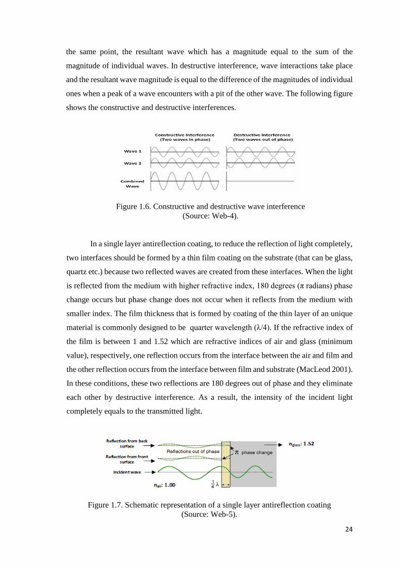
In a single layer antireflection coating, to reduce the reflection of light completely,
two interfaces should be formed by a thin film coating on the substrate (that can be glass,
quartz etc.) because two reflected waves are created from these interfaces. When the light
is reflected from the medium with higher refractive index, 180 degrees (π radians) phase
change occurs but phase change does not occur when it reflects from the medium with
smaller index. The film thickness that is formed by coating of the thin layer of an unique
material is commonly designed to be quarter wavelength (λ/4). If the refractive index of
the film is between 1 and 1.52 which are refractive indices of air and glass (minimum
value), respectively, one reflection occurs from the interface between the air and film and
the other reflection occurs from the interface between film and substrate (MacLeod 2001).
In these conditions, these two reflections are 180 degrees out of phase and they eliminate
each other by destructive interference. As a result, the intensity of the incident light
completely equals to the transmitted light.
Figure 1.7. Schematic representation of a single layer antireflection coating
(Source: Web-5).
25
There is no unique material that has the refractive index needed to reduce
reflectance to zero, in a single layer coating. This is a serious disadvantage of the single
layer antireflection coatings and multilayer antireflection coating is needed. The
multilayer coating efficiently eliminates the reflections over a wider range of the
wavelengths while a single layer coating can reduce the reflection of light at only one
wavelength. Besides, a wide variety of materials can be used appropriately in a multilayer
antireflection coating to completely diminish light transmission losses. In multilayer
antireflection coatings, quarter-quarter, quarter-half-quarter and broadband coating
designs can be applied (Web-5).
1.2.2.2. High Reflection Coating
High reflection (HR) coating is needed for the applications that require high
reflectance and also extremely low scattering and absorption properties like laser
applications. Besides, in many optical systems, mirrors are used and they should have
high reflectivity characteristics in order to increase the performance of these systems.
High reflection coatings play an important role in maintaining the optical durability and
reflectance property (MacLeod 2001). There are two types of high reflection coatings:
dielectric and metallic coatings.
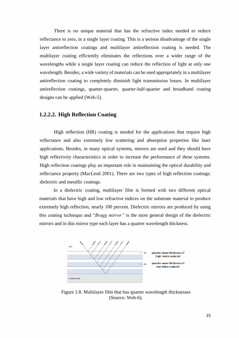
In a dielectric coating, multilayer film is formed with two different optical
materials that have high and low refractive indices on the substrate material to produce
extremely high reflection, nearly 100 percent. Dielectric mirrors are produced by using
this coating technique and “Bragg mirror” is the most general design of the dielectric
mirrors and in this mirror type each layer has a quarter wavelength thickness.
Figure 1.8. Multilayer film that has quarter wavelength thicknesses
(Source: Web-6).
26
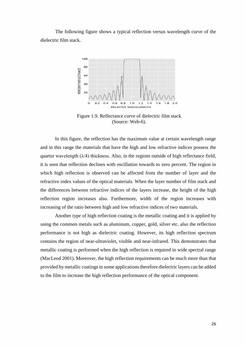
The following figure shows a typical reflection versus wavelength curve of the
dielectric film stack.
Figure 1.9. Reflectance curve of dielectric film stack
(Source: Web-6).
In this figure, the reflection has the maximum value at certain wavelength range
and in this range the materials that have the high and low refractive indices possess the
quarter wavelength (λ/4) thickness. Also, in the regions outside of high reflectance field,
it is seen that reflection declines with oscillation towards to zero percent. The region in
which high reflection is observed can be affected from the number of layer and the
refractive index values of the optical materials. When the layer number of film stack and
the differences between refractive indices of the layers increase, the height of the high
reflection region increases also. Furthermore, width of the region increases with
increasing of the ratio between high and low refractive indices of two materials.
Another type of high reflection coating is the metallic coating and it is applied by
using the common metals such as aluminum, copper, gold, silver etc. also the reflection
performance is not high as dielectric coating. However, its high reflection spectrum
contains the region of near-ultraviolet, visible and near-infrared. This demonstrates that
metallic coating is performed when the high reflection is required in wide spectral range
(MacLeod 2001). Moreover, the high reflection requirements can be much more than that
provided by metallic coatings in some applications therefore dielectric layers can be added
to the film to increase the high reflection performance of the optical component.
27
1.2.2.3. Partial Reflectors
Beam splitters are known as partial reflectors which reflect the incident light ray
not completely but partially and some parts of the light ray are transmitted. This type of
optical component is generated with the metal coating on generally glass substrate and
the metal selection is performed according to the reflection and transmission
characteristics. Beam splitters have a plane surface and commonly their surface are
inclined to realize the separating of the light ray into transmitted and reflected parts and
percentages of them alter according to the application but generally beam splitters have
equal percentage of transmission and reflection as 50/50 (T/R) (MacLeod 2001).
Moreover, silver is common metal type used in the metal deposition process on the
substrate.
1.2.2.4. Optical Filters
Optical filters are optical components that are designed to have selective
transmissivity and rejection property against certain wavelengths or ranges of
wavelengths. They are utilized in a variety of applications such as lasers systems, imaging,
defense and sensing applications. There are distinct types of filters as bandpass filters,
notch filters and edge filters. For all these filter types, single or multilayer film stacks that
have quarter wavelength thickness and also antireflection coatings explained the previous
sections can be applied according to the requirements by using suitable optical materials
in terms of transmission and reflection properties (MacLeod 2001).
The bandpass filters transmit a certain range of wavelengths and reject all the
others whereas the notch filters are design to reject a certain range of wavelengths and
transmit all the others. In addition to these types, edge filters are defined as the filters that
transmit the wavelengths which are over or beneath given values therefore they can be
categorized as longwave pass and shortwave pass filters (MacLeod 2001). Also, hot and
cold mirrors that are known as heat control filters are other types of edge filters. The hot
mirror is formed by coating on the glass substrate, generally borosilicate glass, with
multilayer dielectric coating technique and it has the unique property as reducing
temperature of the light beam through the reflection of heat. The hot mirrors transmit
approximately 85% of visible light, which is in the region between 420 and 700nm and
28
reflect nearly 95% of infrared (IR) radiation, range between 750-1100nm (Web-7 , Web-
8). Moreover, the same coating technique is used for the cold mirrors like hot mirrors
however the cold mirrors are designed to reflect the visible light as nearly 95% and
transmit the 85% of infrared radiation. The hot and cold mirrors are commonly used in
projection, illumination systems and scientific instruments (Web-7 , Web-8).
There are several types of coating production methods. In addition to application
requirements, optical, mechanical and chemical properties, evaporation or condensation
properties and also the cost of the materials are very significant points for selecting
suitable coating method. In the next section, the coating production methods will be
discussed clearly.
1.2.3. Thin Film Production Methods
Thin film optical coatings are fabricated using optical materials on desired
substrates by using compatible methods. The material selection need to be done carefully
for the thin film deposition methods because all optical materials have different properties
thus they must comply with distinct operating conditions. For instance, the materials in
the oxide class are used in the applications in the visible and near-infrared region while
in the ultraviolet region, fluorides are used instead of oxides.
Although there are many types of the deposition processes for thin film coatings,
generally they are operated under vacuum conditions thus they can be grouped into two
main headings as physical vapor deposition (PVD) and chemical vapor deposition (CVD)
(Träger 2012).
Physical Vapor Deposition (PVD):
In PVD processes, the main goal is the deposition of thin film coating by
condensation of the desired material from the vapor phase. PVD also can be categorized
into two diverse process types as thermal evaporation and energetic.
Thermal evaporation is a simple method to produce thin films. In this method, the
desired thin film material is heated under vacuum and then evaporated material condenses
on the substrate to form thin film coating. In energetic processes, extra energy is
supplemented to the process to facilitate the movement of condensing particles that are
29
effective in thin film coating. Energetic processes include the most common methods as
cathodic arc deposition, ion assisted deposition and sputter deposition.
In the cathodic arc deposition, vacuum conditions are supplied and low voltage
and high current are applied to the system, then arc is created on the cathode surface. The
temperature reaches quite high values at the points on the cathode surface where the arc
forms, as a result of this, the desired materials are evaporated from the cathode and then
highly ionized plasma composed of evaporated materials takes place and materials are
deposited on the substrate under vacuum (Piegari and Flory 2013). The abrasion resistant
and rigid coatings are produced with this method. Ion assisted deposition (IAD) is another
PVD process and is also called as ion beam assisted deposition (IBAD). In this method,
high vacuum conditions are provided like the cathodic arc deposition and desired coating
material is evaporated by using an electron beam evaporator. After that, the coating
molecules condense and cling to the substrate surface and at the same time ion beam
bombardment which helps achieving desired density of the film (Träger 2012). The last
method is the sputter deposition and in this method, the vacuum is supplied again in the
system like the other energetic processes. The target material that is desired to be coated
on the substrate forms the cathode while the substrate is located in the anode. The plasma
is generated with gas ionization. Argon is common choice for gas. Ions strike to the
surface of the target material and they remove atoms and molecules from there. This event
is called as sputtering. Thereafter, ejected atoms and molecules from the target material
condense and deposit on the substrate hence thin film coating is produced (Träger 2012,
Piegari and Flory 2013).
Chemical Vapor Deposition (CVD):
CVD processes are similar to the PVD processes but the important difference is
that chemical reaction takes place in CVD processes. The gaseous reactants called as
precursors are carried into the reaction chamber under vacuum conditions, sometimes by
using carrier gases, then deposition occurs on substrate and thin film coating is achieved
(Piegari and Flory 2013). There are many types of CVD processes and diversity between
them has evolved due to a variety of reaction activation techniques such as plasma
enhanced, photo initiated and hot wire although there are other reasons such as reactor
type and cost (Träger 2012). CVD is commonly utilized in thin and hard film coatings to
ensure preservation of the coated product against external influences.
30
In the plasma enhanced chemical vapor deposition (PECVD), electrical energy is
utilized instead of thermal energy used in general CVD process to provide the activation
of the reaction (Pierson 1999). In this technique, plasma is created from the reactant gases
via electrical energy and from that plasma a solid layer is formed on the desired substrate
(Jones and Hitchman 2009). When it is compared with CVD, the significant point in this
technique is that approximately 250-350oC is enough substrate temperature value to
execute the deposition process whereas temperature is needed in common CVD process
is nearly 800oC (Pierson 1999). Photo initiated chemical vapor deposition (PICVD) is
another CVD technique and UV light is used to generate photo-initiators that trigger free
radical polymerization reaction and heat is not needed to perform the deposition as in
plasma enhanced CVD (Pierson 1999). More regular structured polymers are created by
this technique compared to PECVD (Dorval Dion and Tavares 2013). Hot wire chemical
vapor deposition (HWCVD) is a thermal CVD process in which reaction takes place by
heat. In this technique, heat is supplied to the gas mixture for the decomposition of
chemical by the hot wire then reaction is started and after a certain time, layer is formed
on the substrate. The main disadvantage of this technique is that there is a restriction in
polymeric materials deposition. Monomers that will be used in the HWCVD process
might not be resistant to the heat and when they undergo to thermal conditions, some of
them decompose (Dorval Dion and Tavares 2013).
In addition to these methods, there is also a coating technique that is very similar
to CVD processes called as atomic layer deposition (ALD). The main difference between
these two methods is that in CVD process, various precursors can be delivered to the
reaction chamber at the same time to generate the coating film, on the other hand, in the
ALD technique, the desired precursors are transported consecutively into the reactor
under vacuum (Johnson, Hultqvist et al. 2014). Owing to carrying of the various
precursors successively into the reactor, individual reactions occur by each precursor. The
reaction takes place completely on the surface of the substrate by striking of the first
precursor to the surface and only one atomic layer is produced. After that, the new
monolayer is deposited on the layer which was formed previously and this process
continues and can be cycled until the desired film is obtained. Besides, the important thing
during the ALD process is that after forming monolayer by the precursor, purging
operation is done by using the inert gas like nitrogen or argon in order to eliminate
unwanted byproducts occurred in the reaction and this is maintained after every layer is
created. Therefore, ALD is slow process but there are many significant advantages as
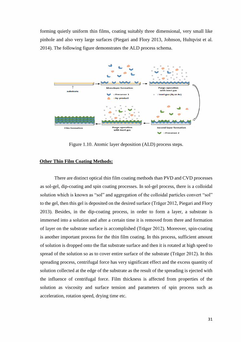
31
forming quietly uniform thin films, coating suitably three dimensional, very small like
pinhole and also very large surfaces (Piegari and Flory 2013, Johnson, Hultqvist et al.
2014). The following figure demonstrates the ALD process schema.
Figure 1.10. Atomic layer deposition (ALD) process steps.
Other Thin Film Coating Methods:
There are distinct optical thin film coating methods than PVD and CVD processes
as sol-gel, dip-coating and spin coating processes. In sol-gel process, there is a colloidal
solution which is known as “sol” and aggregation of the colloidal particles convert “sol”
to the gel, then this gel is deposited on the desired surface (Träger 2012, Piegari and Flory
2013). Besides, in the dip-coating process, in order to form a layer, a substrate is
immersed into a solution and after a certain time it is removed from there and formation
of layer on the substrate surface is accomplished (Träger 2012). Moreover, spin-coating
is another important process for the thin film coating. In this process, sufficient amount
of solution is dropped onto the flat substrate surface and then it is rotated at high speed to
spread of the solution so as to cover entire surface of the substrate (Träger 2012). In this
spreading process, centrifugal force has very significant effect and the excess quantity of
solution collected at the edge of the substrate as the result of the spreading is ejected with
the influence of centrifugal force. Film thickness is affected from properties of the
solution as viscosity and surface tension and parameters of spin process such as
acceleration, rotation speed, drying time etc.
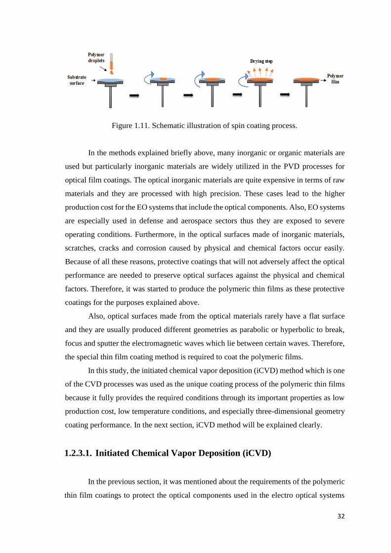
32
Figure 1.11. Schematic illustration of spin coating process.
In the methods explained briefly above, many inorganic or organic materials are
used but particularly inorganic materials are widely utilized in the PVD processes for
optical film coatings. The optical inorganic materials are quite expensive in terms of raw
materials and they are processed with high precision. These cases lead to the higher
production cost for the EO systems that include the optical components. Also, EO systems
are especially used in defense and aerospace sectors thus they are exposed to severe
operating conditions. Furthermore, in the optical surfaces made of inorganic materials,
scratches, cracks and corrosion caused by physical and chemical factors occur easily.
Because of all these reasons, protective coatings that will not adversely affect the optical
performance are needed to preserve optical surfaces against the physical and chemical
factors. Therefore, it was started to produce the polymeric thin films as these protective
coatings for the purposes explained above.
Also, optical surfaces made from the optical materials rarely have a flat surface
and they are usually produced different geometries as parabolic or hyperbolic to break,
focus and sputter the electromagnetic waves which lie between certain waves. Therefore,
the special thin film coating method is required to coat the polymeric films.
In this study, the initiated chemical vapor deposition (iCVD) method which is one
of the CVD processes was used as the unique coating process of the polymeric thin films
because it fully provides the required conditions through its important properties as low
production cost, low temperature conditions, and especially three-dimensional geometry
coating performance. In the next section, iCVD method will be explained clearly.
1.2.3.1. Initiated Chemical Vapor Deposition (iCVD)
In the previous section, it was mentioned about the requirements of the polymeric
thin film coatings to protect the optical components used in the electro optical systems
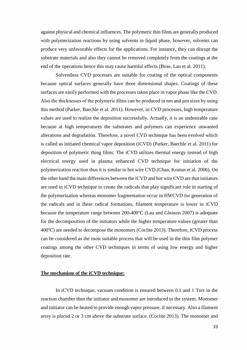
33
against physical and chemical influences. The polymeric thin films are generally produced
with polymerization reactions by using solvents in liquid phase, however, solvents can
produce very unfavorable effects for the applications. For instance, they can disrupt the
substrate materials and also they cannot be removed completely from the coatings at the
end of the operations hence this may cause harmful effects (Bose, Lau et al. 2011).
Solventless CVD processes are suitable for coating of the optical components
because optical surfaces generally have three dimensional shapes. Coatings of these
surfaces are easily performed with the processes taken place in vapor phase like the CVD.
Also the thicknesses of the polymeric films can be produced in nm and µm sizes by using
this method (Parker, Baechle et al. 2011). However, in CVD processes, high temperature
values are used to realize the deposition successfully. Actually, it is an undesirable case
because at high temperatures the substrates and polymers can experience unwanted
alterations and degradation. Therefore, a novel CVD technique has been evolved which
is called as initiated chemical vapor deposition (iCVD) (Parker, Baechle et al. 2011) for
deposition of polymeric thing films. The iCVD utilizes thermal energy instead of high
electrical energy used in plasma enhanced CVD technique for initiation of the
polymerization reaction thus it is similar to hot wire CVD (Chan, Kostun et al. 2006). On
the other hand the main differences between the iCVD and hot wire CVD are that initiators
are used in iCVD technique to create the radicals that play significant role in starting of
the polymerization whereas monomer fragmentation occur in HWCVD for generation of
the radicals and in these radical formations, filament temperature is lower in iCVD
because the temperature range between 200-400oC (Lau and Gleason 2007) is adequate
for the decomposition of the initiators while the higher temperature values (greater than
400oC) are needed to decompose the monomers (Coclite 2013). Therefore, iCVD process
can be considered as the most suitable process that will be used in the thin film polymer
coatings among the other CVD techniques in terms of using low energy and higher
deposition rate.
The mechanism of the iCVD technique:
In iCVD technique, vacuum condition is ensured between 0.1 and 1 Torr in the
reaction chamber then the initiator and monomer are introduced to the system. Monomer
and initiator can be heated to provide enough vapor pressure, if necessary. Also a filament
array is placed 2 or 3 cm above the substrate surface. (Coclite 2013). The monomer and
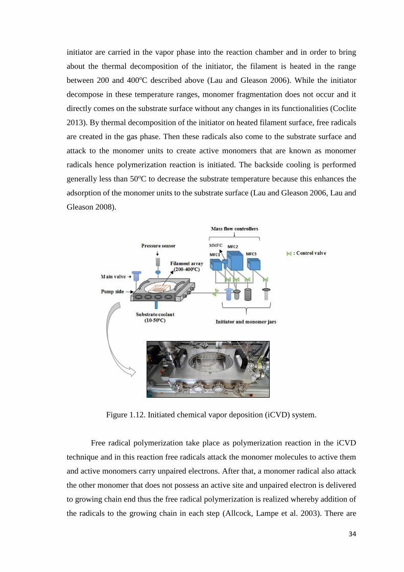
34
initiator are carried in the vapor phase into the reaction chamber and in order to bring
about the thermal decomposition of the initiator, the filament is heated in the range
between 200 and 400oC described above (Lau and Gleason 2006). While the initiator
decompose in these temperature ranges, monomer fragmentation does not occur and it
directly comes on the substrate surface without any changes in its functionalities (Coclite
2013). By thermal decomposition of the initiator on heated filament surface, free radicals
are created in the gas phase. Then these radicals also come to the substrate surface and
attack to the monomer units to create active monomers that are known as monomer
radicals hence polymerization reaction is initiated. The backside cooling is performed
generally less than 50oC to decrease the substrate temperature because this enhances the
adsorption of the monomer units to the substrate surface (Lau and Gleason 2006, Lau and
Gleason 2008).
Figure 1.12. Initiated chemical vapor deposition (iCVD) system.
Free radical polymerization take place as polymerization reaction in the iCVD
technique and in this reaction free radicals attack the monomer molecules to active them
and active monomers carry unpaired electrons. After that, a monomer radical also attack
the other monomer that does not possess an active site and unpaired electron is delivered
to growing chain end thus the free radical polymerization is realized whereby addition of
the radicals to the growing chain in each step (Allcock, Lampe et al. 2003). There are
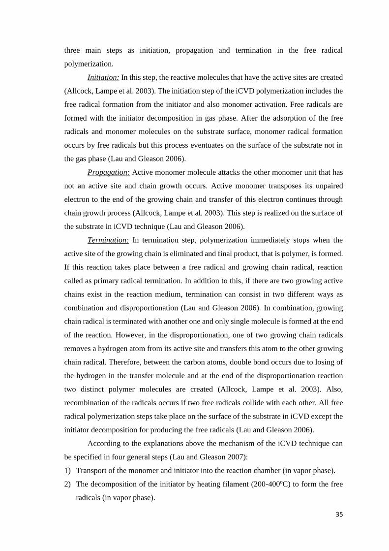
35
three main steps as initiation, propagation and termination in the free radical
polymerization.
Initiation: In this step, the reactive molecules that have the active sites are created
(Allcock, Lampe et al. 2003). The initiation step of the iCVD polymerization includes the
free radical formation from the initiator and also monomer activation. Free radicals are
formed with the initiator decomposition in gas phase. After the adsorption of the free
radicals and monomer molecules on the substrate surface, monomer radical formation
occurs by free radicals but this process eventuates on the surface of the substrate not in
the gas phase (Lau and Gleason 2006).
Propagation: Active monomer molecule attacks the other monomer unit that has
not an active site and chain growth occurs. Active monomer transposes its unpaired
electron to the end of the growing chain and transfer of this electron continues through
chain growth process (Allcock, Lampe et al. 2003). This step is realized on the surface of
the substrate in iCVD technique (Lau and Gleason 2006).
Termination: In termination step, polymerization immediately stops when the
active site of the growing chain is eliminated and final product, that is polymer, is formed.
If this reaction takes place between a free radical and growing chain radical, reaction
called as primary radical termination. In addition to this, if there are two growing active
chains exist in the reaction medium, termination can consist in two different ways as
combination and disproportionation (Lau and Gleason 2006). In combination, growing
chain radical is terminated with another one and only single molecule is formed at the end
of the reaction. However, in the disproportionation, one of two growing chain radicals
removes a hydrogen atom from its active site and transfers this atom to the other growing
chain radical. Therefore, between the carbon atoms, double bond occurs due to losing of
the hydrogen in the transfer molecule and at the end of the disproportionation reaction
two distinct polymer molecules are created (Allcock, Lampe et al. 2003). Also,
recombination of the radicals occurs if two free radicals collide with each other. All free
radical polymerization steps take place on the surface of the substrate in iCVD except the
initiator decomposition for producing the free radicals (Lau and Gleason 2006).
According to the explanations above the mechanism of the iCVD technique can
be specified in four general steps (Lau and Gleason 2007):
1) Transport of the monomer and initiator into the reaction chamber (in vapor phase).
2) The decomposition of the initiator by heating filament (200-400oC) to form the free
radicals (in vapor phase).
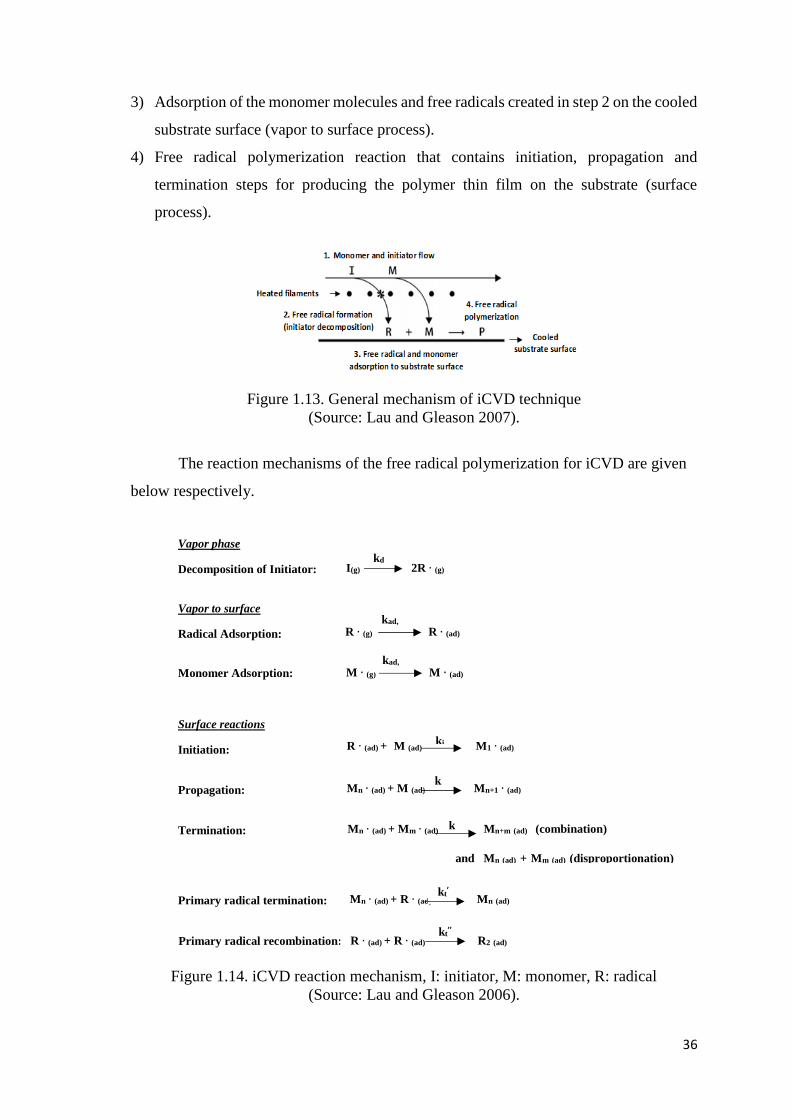
36
3) Adsorption of the monomer molecules and free radicals created in step 2 on the cooled
substrate surface (vapor to surface process).
4) Free radical polymerization reaction that contains initiation, propagation and
termination steps for producing the polymer thin film on the substrate (surface
process).
Figure 1.13. General mechanism of iCVD technique
(Source: Lau and Gleason 2007).
The reaction mechanisms of the free radical polymerization for iCVD are given
below respectively.
Vapor phase
Decomposition of Initiator:
Vapor to surface
Radical Adsorption:
Monomer Adsorption:
Surface reactions
Initiation:
Propagation:
Termination:
Primary radical termination:
Primary radical recombination:
Figure 1.14. iCVD reaction mechanism, I: initiator, M: monomer, R: radical
(Source: Lau and Gleason 2006).
I(g) 2R ∙ (g) kd
R ∙ (g) R ∙ (ad) kad,
R
M ∙ (g) M ∙ (ad) kad,
M
R ∙ (ad) + M (ad) M1 ∙ (ad) ki
Mn ∙ (ad) + M (ad) Mn+1 ∙ (ad) k
p
Mn ∙ (ad) + Mm ∙ (ad) Mn+m (ad) (combination)
and Mn (ad) + Mm (ad) (disproportionation)
k
t
Mn ∙ (ad) + R ∙ (ad) Mn (ad) kt
’
R ∙ (ad) + R ∙ (ad) R2 (ad) kt
’’
37
In these reactions, kd is rate constant for initiator decomposition, kad,R and kad,M are
the adsorption rate constants for radical and monomer, respectively. Also, ki, kp, kt, kt’ and
kt” are the rate constants for initiation, propagation, termination, primary radical
termination and radical recombination, respectively.
Some suitable assumptions should be made to derive the kinetic equations for the
reactions that occur in different steps of the free radical polymerization.
i) The first assumption is the initiation rate, ri, equals to the rate of initiator
decomposition, rd.
𝑟𝑖 = 𝑟𝑑 = 𝑘𝑖 [𝑀][𝑅 ⋅] = 2𝑓𝑘𝑑[𝐼]
In this reaction rate equation, initiating radicals’ fraction is indicated as “f”
(Allcock, Lampe et al. 2003) and from each initiator decomposition, two radicals are
generated thus fraction is multiplied by 2 in the rate equation of the initiator
decomposition. Besides, the termination rate can be expressed as the following relation;
𝑟𝑡 = 2𝑘𝑡 [𝑀 ⋅]2
The growing chain is terminated with the collision of two radicals hence the factor
of 2 presents in the termination rate equation.
ii) The second assumption is the steady state approximation for the total radical
concentration.
𝑑[𝑀 ⋅]
𝑑𝑡= 𝑟𝑖 − 𝑟𝑡 = 0
Equation (1.16) explained that there is no any effect of the reactions in propagating
step on the total radical concentration because in this step radicals are created and
destroyed consecutively (Allcock, Lampe et al. 2003). Therefore the rate of propagating
radicals’ initiation becomes equal to termination rate due to the steady state
approximation. The total radical concentration is found from the following derivation;
(1.14)
(1.15)
(1.16)
38
𝑟𝑖 = 𝑟𝑡
2𝑓𝑘𝑑[𝐼] = 2𝑘𝑡 [𝑀 ⋅]2
[𝑀 ⋅] = ( 𝑓𝑘𝑑[𝐼]
𝑘𝑡)
1/2
Additionally, the rate of polymerization, rp, can be defined as the rate of depletion
of the monomer concentration in accordance with time and this occurs in both initiation
and propagation steps (Allcock, Lampe et al. 2003).
𝑟𝑝 = −𝑑[𝑀]
𝑑𝑡= 𝑘𝑖 [𝑀][𝑅 ⋅] + 𝑘𝑝 [𝑀][𝑀 ⋅]
iii) The last assumption is the lengths of the kinetic chain which can be expressed
as the number of monomer units consumed per active center are too much. According to
this assumption, it is observed that the number of monomer units depleted in the chain
propagation step are very high when compared with the chain initiation step. Therefore,
rate of polymerization becomes equal to the only rate of propagation (Allcock, Lampe et
al. 2003) .
𝑟𝑝 = −𝑑[𝑀]
𝑑𝑡= 𝑘𝑝 [𝑀][𝑀 ⋅]
The kinetic chain length, ʋ, was defined above and it is calculated by dividing of
rate of polymerization to initiation rate (Allcock, Lampe et al. 2003).
𝑣 =𝑟𝑝
𝑟𝑖=
𝑘𝑝 [𝑀][𝑀 ⋅]
𝑘𝑖 [𝑀][𝑅 ⋅]
Furthermore, the number average molecular weight, Mn, is found by multiplying
of the monomer molar mass, Mm, with average degree of polymerization, 𝐷𝑃̅̅ ̅̅ .
The average degree of polymerization can be identified as the number average
monomer molecule in a polymer. And after a certain derivations, the following equation
was obtained and by using this equation 𝐷𝑃̅̅ ̅̅ is calculated easily.
(1.17)
(1.18)
(1.19)
(1.20)
39
𝐷𝑃̅̅ ̅̅ = 2𝑣 (𝑘𝑡𝑐 + 𝑘𝑡𝑑
𝑘𝑡𝑐 + 2𝑘𝑡𝑑)
In equation (1.22), ktc and ktd are the rate constants for the termination by
combination and disproportionation, respectively. Besides, if combination takes place
mainly in the termination step in spite of disproportionation, 𝐷𝑃̅̅ ̅̅ becomes equal to 2ʋ, in
the opposite case, it equals to ʋ.
Literature Survey for iCVD:
There are different types of polymeric materials produced by using iCVD for thin
film coatings as acrylates, methacrylates, polytetrafluoroethylene (PTFE), styrenes,
crosslinked polymers which are hydrogels and also copolymers (Bose, Lau et al. 2011).
Additionally, these polymers have distinct properties, for examples, while some of them
have superhydrophobic (Lau and Gleason 2007), superhydrophilic or antimicrobial
(Martin, Lau et al. 2007) properties, the other ones possess low dielectric constants
(Trujillo, Wu et al. 2010) or display some responsive features (Alf, Hatton et al. 2011) in
terms of temperature or pH (Alf, Hatton et al. 2011, Coclite 2013). iCVD technique has
a wide range of the application areas such as drug delivery, dielectric coatings, biosensors,
and barrier coatings for protection of optical and electro optical systems owing to coating
varies type of the polymers specified above.
In 2007, Martin and co-workers studied the polymeric antimicrobial coating,
which prevents the growth of the Escherichia coli and Bacillus subtilis bacteria, on nylon
fabric by iCVD technique and in this study dimethylaminomethylstyrene (DMAMS) was
used as monomer due to having antimicrobial property. As initiator di-tert-amylperoxide
(TAP) was utilized. iCVD method was preferred for coating the nylon fabric dyed with
camouflage pattern that possesses porous structure because during coating process the
clogging of pores and damaging dyed fabric by organic solvents were undesirable cases
in this study. As the operating conditions, 331oC filament temperature, room temperature
for substrate, 200 mTorr total pressure and 2.0 and 0.6 sccm monomer and initiator flow
rates were used by the Martin and co-workers. According to the results of the tests, it was
concluded that the coating was highly protective (99.99%) against gram negative E. coli
and gram positive B. subtilis also there were no blockage in the pores and also any
changes in color or feel of the fabric (Martin, Kooi et al. 2007).
(1.21)
40
Another study related with the biological field like the Martin and co-workers
study was performed by Chan et al. as polymeric coating produced with iCVD for the
application of antibiofouling surface. The hydrophilicity is very crucial property for the
polymers that are used in the biomedical applications and polyvinylpyrrolidone (PVP)
has this special feature also it is significant biocompatible polymer. In this study, Chan
and co-workers were discussed that the PVP homopolymer and copolymer created with
ethylene glycol diacrylate (EDGA) and vinylpyrrolidone (VP) coatings on silicon
substrate were performed properly or not by using iCVD technique and observations were
made regarding the functionality of the polymer. Also, effect of the VP flow rate was
examined on the deposition rate. Tert-butyl peroxide (TBPO) was used as initiator in the
operations. Results of this study indicated that there was a direct proportion between the
deposition rate and partial pressure of monomer, also the hydrophilicity feature of PVP
was conserved after coating with iCVD, in addition, copolymer coating performed
efficiently with vapor flow control and supplied the property of swelling in water to the
polymer (Chan, Kostun et al. 2006).
iCVD method is used not only for the flat or three dimensional shaped surfaces
also it can be applied to particle substrates by producing encapsulating layers of polymers.
There are many studies about polymeric coatings on particles and one of them was
performed by Lau and Gleason. In their study, encapsulation layer around active particles,
fluorescein in this study, was produced with copolymer that generated with the
methacrylic acid (MAA) and ethyl acrylate (EA) and TBPO initiator by using iCVD
method. Then, it was observed that copolymer coating that has property of swelling
depending on pH ensured releasing of active materials in a controlled manner at certain
pH values. While uncoated particles were released at pH of 1.2 and 6.8 in a short time,
copolymer encapsulation did not allow releasing of fluorescein at pH 1.2 but facilitated
fluorescein diffusion at pH 6.8 because of swelling (Lau and Gleason 2008).
Encapsulation of the particles by iCVD was performed also again Lau and Gleason
in a different study. In this study encapsulation process was implemented for three
different goals to create superhydrophobic surface, reactive surface and providing
controlling drug release like the previous study. To generate the superhydrophobic
surface that is important with regard to ensuring the self-cleaning feature, the carbon
nanotubes arranged vertically were coated via polytetrafluoroethylene (PTFE) by using
iCVD and as an initiator perfluorobutane-1-sulfonyl fluoride (PFBSF) was used. Water
contact angle should be greater than 150o to for a superhydrophobic surface and water
41
contact angle was observed as approximately 170o by Lau and Gleason. Thus, it was
concluded that carbon nanotubes coated with PTFE had the superhydrophobic property.
Glycidyl methacrylate (GMA) was used as monomer for producing reactive coatings on
glass microspheres and carbon nanotubes because PGMA showed the reactive feature
owing to having epoxide ring. The reason for encapsulation of the particles was that
providing the attachment of functional molecules to PGMA thus some properties altered.
For instance, some aromatic molecules attached to the PGMA coating and thickness
increased thus this caused to increase the refractive index of coating. And the last section
of this study was the encapsulation process for the drug release. Ibuprofen was used as
active particle and similar results with previous study were obtained as avoiding drug
release at low pH value whereas allowing at higher pH value, that is, neutral pH (Lau and
Gleason 2007).
Polymer coatings on the several material surfaces ensure possessing distinct
properties to coated materials and this capability has led to evolve the smart coating idea
for the materials. From the environment different stimuli reach to the materials and smart
coatings responds as required. The most common ones are the pH and temperature
responsive polymeric surfaces and these polymeric coatings produced by iCVD technique
uniformly. For these coatings the unique polymers are used that have responsive property
such as methacrylic acid (MAA) copolymers and polyhydroxyethyl methacrylate
(PHEMA) hydrogels for pH responsive and polyN-isopropylacrylamide (pNIPAAm) for
thermal responsive property (Coclite 2013). About the smart surfaces, Alf et al.
investigated the creating thermal responsive surface of p(NIPAAm-co-DEGDVE)
copolymer that generating the addition of diethylene glycol divinyl ether (DEGDVE)
cross linker with (pNIPAAm) to the iCVD system. p(NIPAAm) has thermal responsive
feature but copolymer was used in this study for providing durability against chain
dissociation. 200oC and 50oC filament and substrate temperature were used respectively
and TBPO was used as an initiator. Temperature responsivity was measured according to
the low critical solution temperature (LCST). If the temperature is lower than the LCST
that is 32oC for p(NIPAAm), polymer swells because of hydrophilicity and random coil
shape occurs. However, when the temperature is higher than the LCST, globular shape
forms. The shape changes depending on temperature stimuli were measured by using
quartz crystal microbalance with dissipation (QCM-D) by Alf et al. According to the
results, they concluded that the highly thermal responsive p(NIPAAm-co-DEGDVE)
42
copolymer coating created as uniformly with iCVD method and produced film could be
used suitably in necessary applications (Alf, Hatton et al. 2011).
iCVD is an important CVD method preferred in the semiconductor industry except
from the other application areas specified previously. Especially, in semiconductor
industry, the integrated circuits undergo the changes continuously in terms of scaling of
interconnect structures thus the interlayer dielectric (ILD) materials improved to meet the
requirements. Besides, the low dielectric constant, k, ILD materials are developed because
the materials having high k values cause occurring some undesired cases as high power
consumption, forming cross talk, high delay time of signal distribution and increasing
heat spread. There are many applications to overcome these problems with creating new
low k materials and one of them was studied by the Trujillo and co-workers. In this study,
polymer that have low k value was coated by using iCVD method. Among the aims of
this study, using environmentally friendly process was one of the most important goal.
PECVD was used in previous studies but the high energy consumption take place during
the process therefore Trujillo et al. preferred to study with iCVD method which uses low
energy and also with iCVD the film composition is adjusted appropriately. 1, 3, 5, 7-
tetravinyltetramethylcylclotetrasiloxane (V4D4) was used as monomer because of similar
structure presents in the V4D4 monomer with common low k monomer used in PECVD
method. The results indicated that the mechanical properties of the film produced with
p(V4D4) polymer by using iCVD developed with regard to modulus and hardness while
the dielectric constant decreased and also it was observed that polymer functionality was
not undergone any changes after coating. They were asserted that iCVD method permitted
the removal of undesirable organic components and used low energy thus it was
considered as environmentally friendly process (Trujillo, Wu et al. 2010).
In addition to all these application areas identified above, iCVD method can be
utilized in producing protective polymer coatings for the optical components. The
significant point is that the optic properties of the substrate material should not be affected
from the polymeric coatings and also these components used in the adverse operating
conditions in the electro optical systems therefore durability, self-cleaning property and
reprocessing are the other crucial desired cases. In literature, there is not any study about
the protective polymeric coatings on the optical components produced by iCVD technique
therefore this study is quite unique compared to the other iCVD studies.
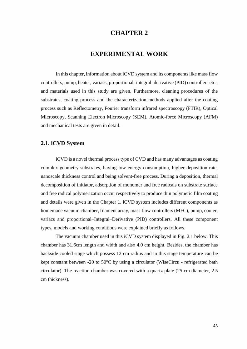
43
CHAPTER 2
EXPERIMENTAL WORK
In this chapter, information about iCVD system and its components like mass flow
controllers, pump, heater, variacs, proportional–integral–derivative (PID) controllers etc.,
and materials used in this study are given. Furthermore, cleaning procedures of the
substrates, coating process and the characterization methods applied after the coating
process such as Reflectometry, Fourier transform infrared spectroscopy (FTIR), Optical
Microscopy, Scanning Electron Microscopy (SEM), Atomic-force Microscopy (AFM)
and mechanical tests are given in detail.
2.1. iCVD System
iCVD is a novel thermal process type of CVD and has many advantages as coating
complex geometry substrates, having low energy consumption, higher deposition rate,
nanoscale thickness control and being solvent-free process. During a deposition, thermal
decomposition of initiator, adsorption of monomer and free radicals on substrate surface
and free radical polymerization occur respectively to produce thin polymeric film coating
and details were given in the Chapter 1. iCVD system includes different components as
homemade vacuum chamber, filament array, mass flow controllers (MFC), pump, cooler,
variacs and proportional–Integral–Derivative (PID) controllers. All these component
types, models and working conditions were explained briefly as follows.
The vacuum chamber used in this iCVD system displayed in Fig. 2.1 below. This
chamber has 31.6cm length and width and also 4.0 cm height. Besides, the chamber has
backside cooled stage which possess 12 cm radius and in this stage temperature can be
kept constant between -20 to 50oC by using a circulator (WiseCircu - refrigerated bath
circulator). The reaction chamber was covered with a quartz plate (25 cm diameter, 2.5
cm thickness).
44
Figure 2.1. Vacuum chamber of iCVD system.
A filament array placed into the reaction chamber was used to supply thermal
energy for decomposition of the initiator and there is space between cooled stage and
Nichrome filaments (80% Ni/20% Cr) approximately 2 or 3 cm. Different filament
temperatures between 230 and 330oC were used in this study and the temperature was
measured by a thermocouple (Type K, Omega Engineering) attached to one of the
filaments. The reactor pressure was kept between 0.1 to 1 Torr using the pump (2XZ-
Rotary Vacuum Pump). To control the pressure in the reaction chamber, exhaust throttling
butterfly valve (Model 253B, MKS type) was used. The monomers which needs to be
heated were installed to the second channel of the system that was heated with heating
tapes (Model FGR rope heater, Omegalux) and they transferred into the reaction chamber
with mass flow controller 2, MFC2, (Model 1150C, MKS type). Other monomers and
initiator were kept at room temperature and they were transferred into the reaction
chamber by using first, third or fourth channel according to the flow amount, and MFC1,
MFC3 (Model 1479A, MKS type) or Manual MFC were used in these channels,
respectively. Furthermore, AC current was provided to some parts of the system like
filaments and heating tapes by using different variacs (Servo-Matik) and PID controllers
(TK4 series, Autonics) were used in order to set and monitor temperatures in certain parts
of the system.
2.2. Materials
In this study polymeric thin films on different substrate materials were fabricated
with iCVD method by using selected monomers (refractive indices between 1.3 and 1.7)
and initiator. Vinyl monomers like acrylate and methacrylate and fluorine-containing
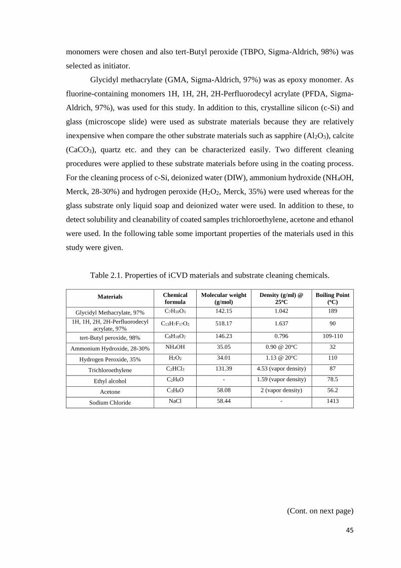
45
monomers were chosen and also tert-Butyl peroxide (TBPO, Sigma-Aldrich, 98%) was
selected as initiator.
Glycidyl methacrylate (GMA, Sigma-Aldrich, 97%) was as epoxy monomer. As
fluorine-containing monomers 1H, 1H, 2H, 2H-Perfluorodecyl acrylate (PFDA, Sigma-
Aldrich, 97%), was used for this study. In addition to this, crystalline silicon (c-Si) and
glass (microscope slide) were used as substrate materials because they are relatively
inexpensive when compare the other substrate materials such as sapphire (Al2O3), calcite
(CaCO3), quartz etc. and they can be characterized easily. Two different cleaning
procedures were applied to these substrate materials before using in the coating process.
For the cleaning process of c-Si, deionized water (DIW), ammonium hydroxide (NH4OH,
Merck, 28-30%) and hydrogen peroxide (H2O2, Merck, 35%) were used whereas for the
glass substrate only liquid soap and deionized water were used. In addition to these, to
detect solubility and cleanability of coated samples trichloroethylene, acetone and ethanol
were used. In the following table some important properties of the materials used in this
study were given.
Table 2.1. Properties of iCVD materials and substrate cleaning chemicals.
Materials Chemical
formula
Molecular weight
(g/mol)
Density (g/ml) @
25oC
Boiling Point
(oC)
Glycidyl Methacrylate, 97% C7H10O3 142.15 1.042 189
1H, 1H, 2H, 2H-Perfluorodecyl
acrylate, 97% C13H7F17O2 518.17 1.637 90
tert-Butyl peroxide, 98% C8H18O2 146.23 0.796 109-110
Ammonium Hydroxide, 28-30% NH4OH 35.05 0.90 @ 20oC 32
Hydrogen Peroxide, 35% H2O2 34.01 1.13 @ 20oC 110
Trichloroethylene C2HCl3 131.39 4.53 (vapor density) 87
Ethyl alcohol C2H6O - 1.59 (vapor density) 78.5
Acetone C3H6O 58.08 2 (vapor density) 56.2
Sodium Chloride NaCl 58.44 - 1413
(Cont. on next page)
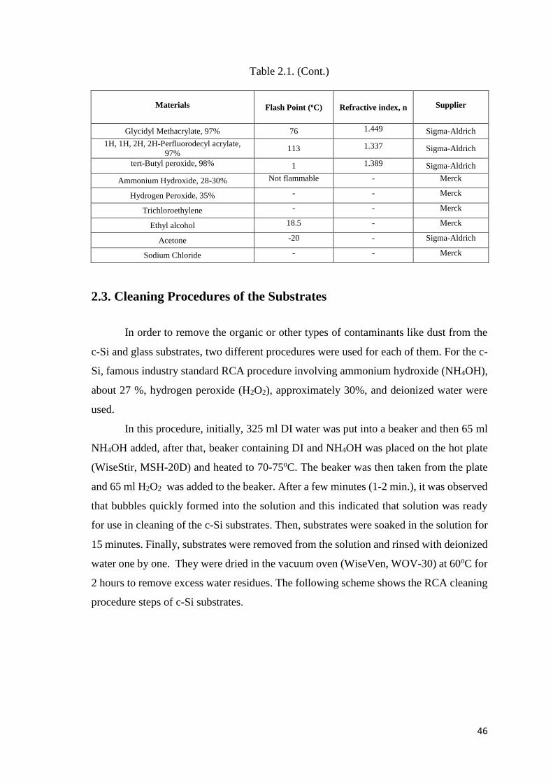
46
Table 2.1. (Cont.)
Materials Flash Point (oC) Refractive index, n Supplier
Glycidyl Methacrylate, 97% 76 1.449 Sigma-Aldrich
1H, 1H, 2H, 2H-Perfluorodecyl acrylate,
97% 113 1.337 Sigma-Aldrich
tert-Butyl peroxide, 98% 1 1.389 Sigma-Aldrich
Ammonium Hydroxide, 28-30% Not flammable - Merck
Hydrogen Peroxide, 35% - - Merck
Trichloroethylene - - Merck
Ethyl alcohol 18.5 - Merck
Acetone -20 - Sigma-Aldrich
Sodium Chloride - - Merck
2.3. Cleaning Procedures of the Substrates
In order to remove the organic or other types of contaminants like dust from the
c-Si and glass substrates, two different procedures were used for each of them. For the c-
Si, famous industry standard RCA procedure involving ammonium hydroxide (NH4OH),
about 27 %, hydrogen peroxide (H2O2), approximately 30%, and deionized water were
used.
In this procedure, initially, 325 ml DI water was put into a beaker and then 65 ml
NH4OH added, after that, beaker containing DI and NH4OH was placed on the hot plate
(WiseStir, MSH-20D) and heated to 70-75oC. The beaker was then taken from the plate
and 65 ml H2O2 was added to the beaker. After a few minutes (1-2 min.), it was observed
that bubbles quickly formed into the solution and this indicated that solution was ready
for use in cleaning of the c-Si substrates. Then, substrates were soaked in the solution for
15 minutes. Finally, substrates were removed from the solution and rinsed with deionized
water one by one. They were dried in the vacuum oven (WiseVen, WOV-30) at 60oC for
2 hours to remove excess water residues. The following scheme shows the RCA cleaning
procedure steps of c-Si substrates.
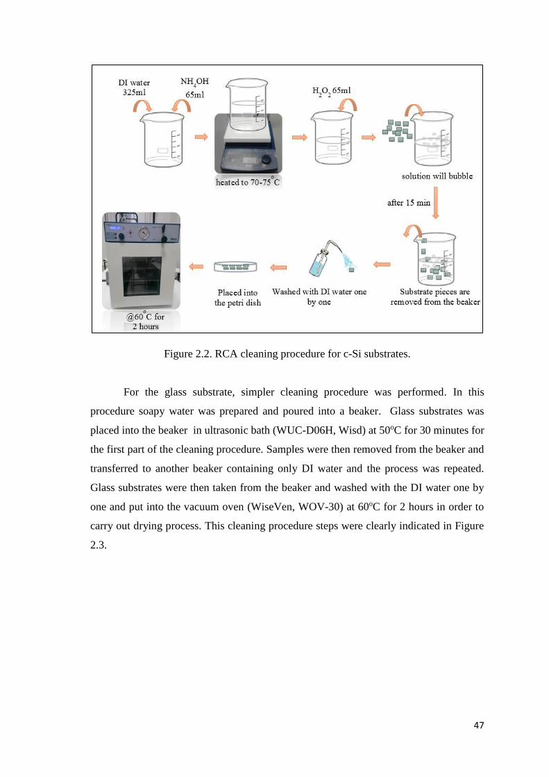
47
Figure 2.2. RCA cleaning procedure for c-Si substrates.
For the glass substrate, simpler cleaning procedure was performed. In this
procedure soapy water was prepared and poured into a beaker. Glass substrates was
placed into the beaker in ultrasonic bath (WUC-D06H, Wisd) at 50oC for 30 minutes for
the first part of the cleaning procedure. Samples were then removed from the beaker and
transferred to another beaker containing only DI water and the process was repeated.
Glass substrates were then taken from the beaker and washed with the DI water one by
one and put into the vacuum oven (WiseVen, WOV-30) at 60oC for 2 hours in order to
carry out drying process. This cleaning procedure steps were clearly indicated in Figure
2.3.
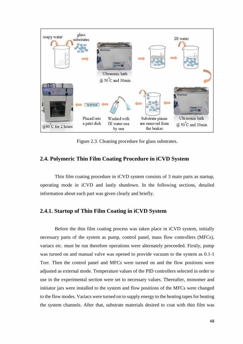
48
Figure 2.3. Cleaning procedure for glass substrates.
2.4. Polymeric Thin Film Coating Procedure in iCVD System
Thin film coating procedure in iCVD system consists of 3 main parts as startup,
operating mode in iCVD and lastly shutdown. In the following sections, detailed
information about each part was given clearly and briefly.
2.4.1. Startup of Thin Film Coating in iCVD System
Before the thin film coating process was taken place in iCVD system, initially
necessary parts of the system as pump, control panel, mass flow controllers (MFCs),
variacs etc. must be run therefore operations were alternately proceeded. Firstly, pump
was turned on and manual valve was opened to provide vacuum to the system as 0.1-1
Torr. Then the control panel and MFCs were turned on and the flow positions were
adjusted as external mode. Temperature values of the PID controllers selected in order to
use in the experimental section were set to necessary values. Thereafter, monomer and
initiator jars were installed to the system and flow positions of the MFCs were changed
to the flow modes. Variacs were turned on to supply energy to the heating tapes for heating
the system channels. After that, substrate materials desired to coat with thin film was
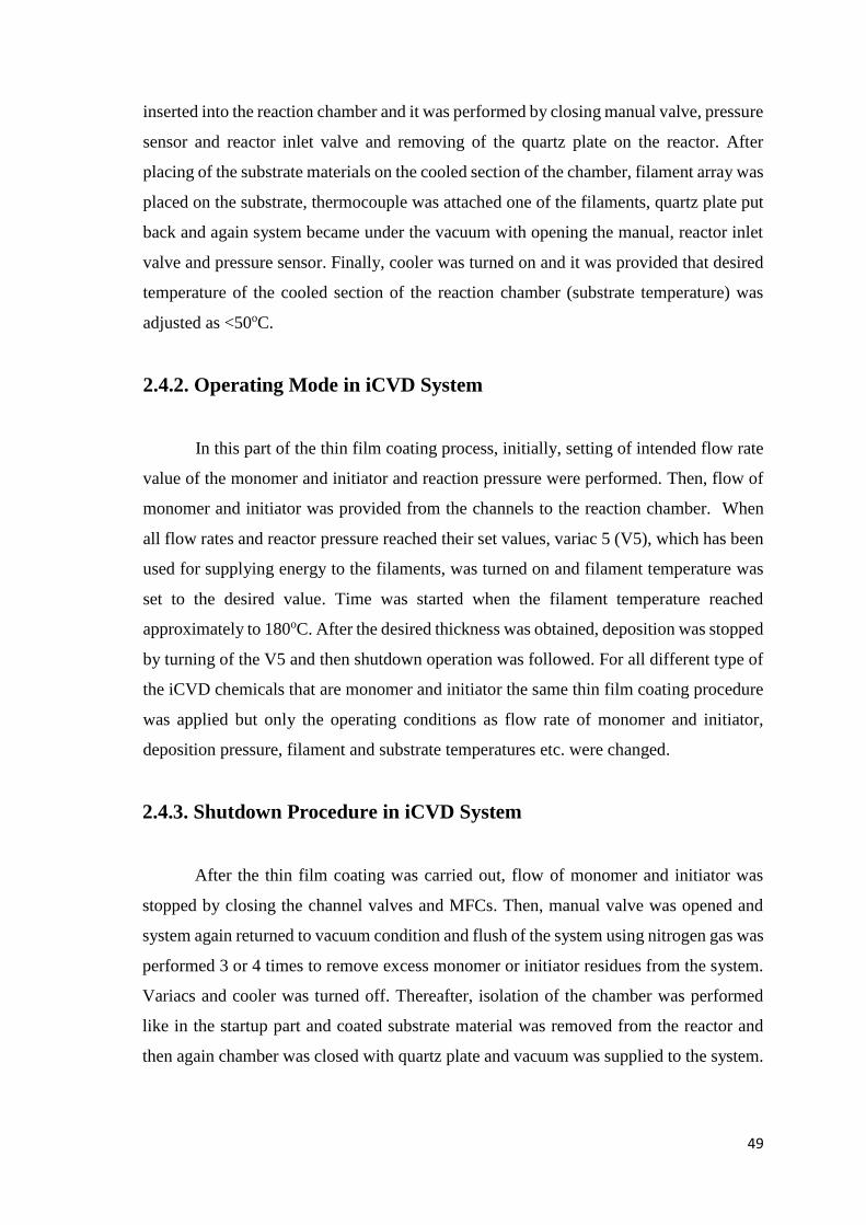
49
inserted into the reaction chamber and it was performed by closing manual valve, pressure
sensor and reactor inlet valve and removing of the quartz plate on the reactor. After
placing of the substrate materials on the cooled section of the chamber, filament array was
placed on the substrate, thermocouple was attached one of the filaments, quartz plate put
back and again system became under the vacuum with opening the manual, reactor inlet
valve and pressure sensor. Finally, cooler was turned on and it was provided that desired
temperature of the cooled section of the reaction chamber (substrate temperature) was
adjusted as <50oC.
2.4.2. Operating Mode in iCVD System
In this part of the thin film coating process, initially, setting of intended flow rate
value of the monomer and initiator and reaction pressure were performed. Then, flow of
monomer and initiator was provided from the channels to the reaction chamber. When
all flow rates and reactor pressure reached their set values, variac 5 (V5), which has been
used for supplying energy to the filaments, was turned on and filament temperature was
set to the desired value. Time was started when the filament temperature reached
approximately to 180oC. After the desired thickness was obtained, deposition was stopped
by turning of the V5 and then shutdown operation was followed. For all different type of
the iCVD chemicals that are monomer and initiator the same thin film coating procedure
was applied but only the operating conditions as flow rate of monomer and initiator,
deposition pressure, filament and substrate temperatures etc. were changed.
2.4.3. Shutdown Procedure in iCVD System
After the thin film coating was carried out, flow of monomer and initiator was
stopped by closing the channel valves and MFCs. Then, manual valve was opened and
system again returned to vacuum condition and flush of the system using nitrogen gas was
performed 3 or 4 times to remove excess monomer or initiator residues from the system.
Variacs and cooler was turned off. Thereafter, isolation of the chamber was performed
like in the startup part and coated substrate material was removed from the reactor and
then again chamber was closed with quartz plate and vacuum was supplied to the system.
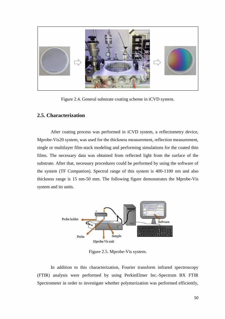
50
Figure 2.4. General substrate coating scheme in iCVD system.
2.5. Characterization
After coating process was performed in iCVD system, a reflectometry device,
Mprobe-Vis20 system, was used for the thickness measurement, reflection measurement,
single or multilayer film-stack modeling and performing simulations for the coated thin
films. The necessary data was obtained from reflected light from the surface of the
substrate. After that, necessary procedures could be performed by using the software of
the system (TF Companion). Spectral range of this system is 400-1100 nm and also
thickness range is 15 nm-50 mm. The following figure demonstrates the Mprobe-Vis
system and its units.
Figure 2.5. Mprobe-Vis system.
In addition to this characterization, Fourier transform infrared spectroscopy
(FTIR) analysis were performed by using PerkinElmer Inc.-Spectrum BX FTIR
Spectrometer in order to investigate whether polymerization was performed efficiently,
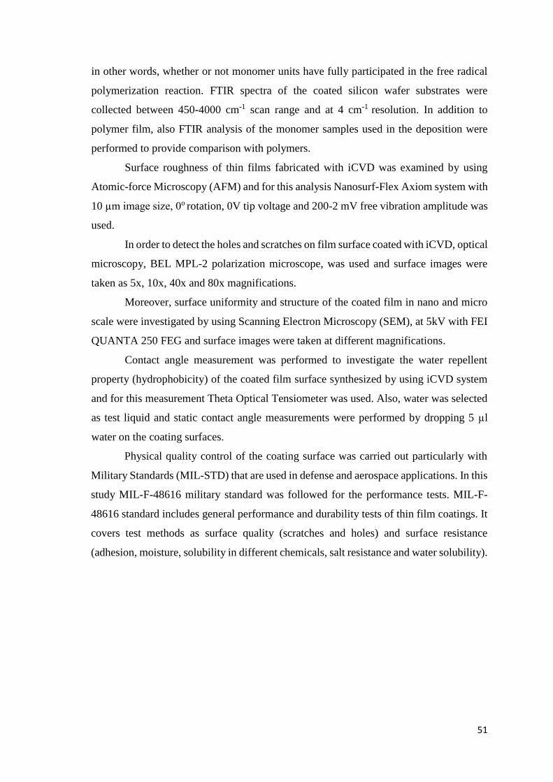
51
in other words, whether or not monomer units have fully participated in the free radical
polymerization reaction. FTIR spectra of the coated silicon wafer substrates were
collected between 450-4000 cm-1 scan range and at 4 cm-1 resolution. In addition to
polymer film, also FTIR analysis of the monomer samples used in the deposition were
performed to provide comparison with polymers.
Surface roughness of thin films fabricated with iCVD was examined by using
Atomic-force Microscopy (AFM) and for this analysis Nanosurf-Flex Axiom system with
10 µm image size, 0o rotation, 0V tip voltage and 200-2 mV free vibration amplitude was
used.
In order to detect the holes and scratches on film surface coated with iCVD, optical
microscopy, BEL MPL-2 polarization microscope, was used and surface images were
taken as 5x, 10x, 40x and 80x magnifications.
Moreover, surface uniformity and structure of the coated film in nano and micro
scale were investigated by using Scanning Electron Microscopy (SEM), at 5kV with FEI
QUANTA 250 FEG and surface images were taken at different magnifications.
Contact angle measurement was performed to investigate the water repellent
property (hydrophobicity) of the coated film surface synthesized by using iCVD system
and for this measurement Theta Optical Tensiometer was used. Also, water was selected
as test liquid and static contact angle measurements were performed by dropping 5 µl
water on the coating surfaces.
Physical quality control of the coating surface was carried out particularly with
Military Standards (MIL-STD) that are used in defense and aerospace applications. In this
study MIL-F-48616 military standard was followed for the performance tests. MIL-F-
48616 standard includes general performance and durability tests of thin film coatings. It
covers test methods as surface quality (scratches and holes) and surface resistance
(adhesion, moisture, solubility in different chemicals, salt resistance and water solubility).
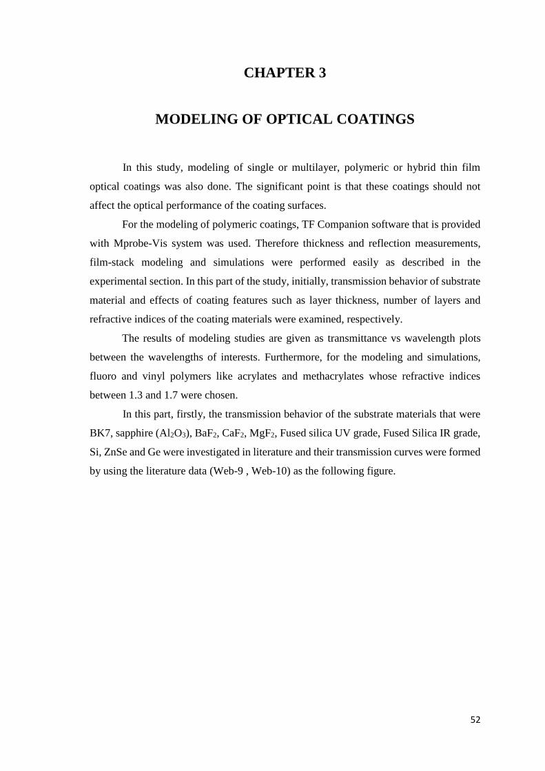
52
CHAPTER 3
MODELING OF OPTICAL COATINGS
In this study, modeling of single or multilayer, polymeric or hybrid thin film
optical coatings was also done. The significant point is that these coatings should not
affect the optical performance of the coating surfaces.
For the modeling of polymeric coatings, TF Companion software that is provided
with Mprobe-Vis system was used. Therefore thickness and reflection measurements,
film-stack modeling and simulations were performed easily as described in the
experimental section. In this part of the study, initially, transmission behavior of substrate
material and effects of coating features such as layer thickness, number of layers and
refractive indices of the coating materials were examined, respectively.
The results of modeling studies are given as transmittance vs wavelength plots
between the wavelengths of interests. Furthermore, for the modeling and simulations,
fluoro and vinyl polymers like acrylates and methacrylates whose refractive indices
between 1.3 and 1.7 were chosen.
In this part, firstly, the transmission behavior of the substrate materials that were
BK7, sapphire (Al2O3), BaF2, CaF2, MgF2, Fused silica UV grade, Fused Silica IR grade,
Si, ZnSe and Ge were investigated in literature and their transmission curves were formed
by using the literature data (Web-9 , Web-10) as the following figure.
53
200 400 600 800 1000 12000
20
40
60
80
100
Tra
nsm
issi
on
(%
)
Wavelength (nm)
BK7
Sapphire (Al2O3)
BaF2
CaF2
MgF2
Fused Silica UV Grade
Fused Silica IR Grade
Si
ZnSe
Ge
Figure 3.1. Transmission curves of substrate materials.
In this graph, wavelength region was selected as 200-1200 nm, which includes the
region of near infrared, visible and far UV, the reason for this, transmission behavior of
the substrate materials was needed to be examined in wide range. According to Figure
3.1, it was observed clearly that all substrate material transmissivity exceeded the point
of 80% except for ZnSe and Silicon in this wavelength region.
Additionally, the effects of thickness and layer number of film stack and refractive
indices of the coating materials were examined in this part. For this reason, substrate
material and polymeric materials had different refractive indices were chosen then
thickness and layer number of the coating were changed separately to monitor their effects
on the transmission and reflection behavior of the substrate. In this system, simulations
were performed easily when the necessary parameters were entered to the related part of
the system software (TF Companion) as transmission range, angle of incident light,
number of point, thickness, layer number of the coating elements etc. and also some
necessary reflection and transmission calculations were performed at the background,
however, the calculation steps were not monitored because only results were given by the
54
software as graphical or tabulated form. In accordance with this purpose, “Bragg mirror”
type reflection expressed in the Chapter 1 as consisting of film stack formed consecutively
with high and low index material was investigated and it was observed that height of the
high reflection zone increases with increasing of the layer number and refractive indices
of the materials and also when the difference of high and low refractive indices increases,
the width of the high reflection zone increases also. In order to demonstrate these effects
clearly by using the reflectometer device, a simple modeling was performed by using
sapphire (Al2O3) as substrate material for simulation owing to obtaining more clear and
prominent thickness and layer number change effects when compare the other substrates.
Besides, poly (methyl methacrylate) (PMMA) and poly (tetrafluoroethylene) (PTFE)
were used in this simulation part as high index (n: 1.49) and low index material (n: 1.32),
respectively. The number of layer in the film stack was identified as 2p+1 where p is pair
and examinations were done according to this information.
Bragg mirror modelling was started with the 100 nm PTFE/100 nm PMMA on
sapphire substrate and number of layer was found as 3 from 2p+1 because there was one
pair. Then, the thickness of the PTFE and PMMA layers were increased from 100 to 150
nm and thickness effects were examined from the following simulation graphs.
Figure 3.2. Film stack model of 1 pair PTFE/PMMA
55
300 400 500 600 700 800 900 1000 1100
86
88
90
92
94
96
98
100
Tra
nsm
itta
nce (
%)
Wavelength (nm)
Figure 3.3. Transmission graphs of 1 layer-100 nm PTFE/100 nm PMMA (black) and 10
layer-150 nm PTFE/150 nm PMMA (red) on sapphire substrates.
According to the Figure 3.3, it was demonstrated clearly that the thickness of the
layer increased from 100 to 150 nm caused to number of sine wave increased and also
high reflection zone shifted to the right side.
After that, the same type film stack was formed but number of pair was increased
from 1 to 10 therefore the number of layer also increased from 3 to 21 by using the 2p+1
relation. Film stack model formed in the Mprobe-Vis system again illustrated in below.
Figure 3.4. Film stack model of 10 pair PTFE/PMMA
56
300 400 500 600 700 800 900 1000 1100
20
30
40
50
60
70
80
90
100
Tran
smit
tan
ce (
%)
Wavelength (nm)
Figure 3.5. Transmission graphs of 10 layer-100 nm PTFE/100 nm PMMA (black) and
10 layer-150 nm PTFE/150 nm PMMA (red) on sapphire substrates.
In the figure above, thickness of layer increased from 100 to 150 nm as 1 pair film
stack and it was observed that number of sine wave again increased when the thickness
of layer improved. In addition to this, when Figure 3.5 was compared with Figure 3.3, it
was represented that the number of pair in the film stack increased from 1 to 10 then the
height of the high reflection zone increased also and this manner could be observed clearly
in Figures 3.3 and 3.5 above.
Finally, the number of pair in the film stack was increased to 100 and according
to the 2p+1 relation the number of layer in film stack was obtained as 201. The film stack
model formed in the software was shown below.
Figure 3.6. Film stack model of 100 pair PTFE/PMMA
57
Thereafter, the necessary parameters were set in the software in order to form the
simulation graphs and two different thickness values were chosen again like the previous
ones to examine and demonstrate the thickness effect and also number of layer changed
in each set to observe the layer number effect. In this section, results obtained from the
software of the Mprobe-Vis system were given in the following figure.
300 400 500 600 700 800 900 1000 1100
0
20
40
60
80
100
Tra
nsm
itta
nce
(%
)
Wavelength (nm)
Figure 3.7. Transmission graphs of 100 layer-100 nm PTFE/100 nm PMMA (black) and
100 layer-150 nm PTFE/150 nm PMMA (red) on sapphire substrates.
When the Figure 3.7 was observed, it was seen that the number of sign wave
increased extremely thus the high reflection zones could be observed more specifically
and the small peaks were eliminated almost wholly with this way. Also, the high reflection
zone shifted to the right side same as the previous ones and as a result of this new
reflection zones came into sight. Moreover, in this section, number of pair was increased
to 100 and total number of layer in the film stack was obtained as 201 by using 2p+1
relation. When this section was compared with the sections of 10 and 1 number of pair, it
was clearly observed that height of the high reflection regions became quite prominent.
Effects of thickness and layer number of film stack were explained and examined
by using all these results given above. Moreover, one of the important aims clarified at
the beginning chapter of the study is that the polymeric thin film coating should not affect
the optical performance of the coated surface, in other words, it was desired that the
polymeric film should not cause a measurable decline of the optical performance of the
coated surface. Therefore, considering this critical point, in this study before the coating
58
process was taken place, modeling was performed to find out what are the optimum film
thickness value does not affect the transmission behaviors of the selected substrates.
In this modeling section, BK7 glass and microscope slides were selected as
substrate materials. However, in the modeling part, c-Si was not selected as a substrate
because it is not a transparent material in the visible spectrum and it only transmits light
in the infrared region as shown in Figure 3.1 previously. Therefore, it was used in the
deposition experiments, and not used in the simulations. As a result, all thickness
measurements and some characterization methods like FTIR were applied by using c-Si
substrate instead of BK7 or microscope slide. Unlike glass substrates, thickness
measurements with reflectometer device after depositions and FTIR characterization were
performed easily, successfully and accurately by using the c-Si substrate.
Glass substrates have surface roughness, thus, some undesired internal reflections
and reflection from stainless steel platform of the reflectometry result in difficulty during
thickness measurements since the reflectometer used in this study is not suitable for
transmission measurements. Various algorithms for reflectivity calculations for
transparent substrates were tried to improve reliability of thickness measurements.
Therefore, very accurate results would not be obtained in the measurements by using BK7
and microscope slide. Microscope slides are more affordable than BK7 due to higher
defect density such as air bubbles and impurities, however, these defects are not clearly
detectable in small volumes. Also, transmission behaviors resemble each other.
Therefore, for the depositions microscope slide and c-Si substrate were used together.
They were placed into reaction chamber and after the deposition, necessary measurements
performed using reference (c-Si) substrate only. Since film thickness does not change with
substrate type, these measurements were very helpful to determine the thickness of
polymer films on glass substrates during and after deposition.
Moreover, poly (glycidyl methacrylate) (PGMA) (n:1.54) and an acrylate
fluoropolymer (FP) was used in modeling. Refractive indices of fluoropolymers that
would be used in this study like Poly(1H,1H,2H,2H-Perfluorodecyl acrylate) (PPFDA)
are generally between 1.34 and 1.37. In addition to PGMA and fluoropolymer, copolymer
consisting of PGMA and FP was used in the modeling. The reason for using a copolymer
is that hydrophobic and self-cleaning properties of FPs and good mechanical properties
of PGMA can be realized with a copolymer film coating.
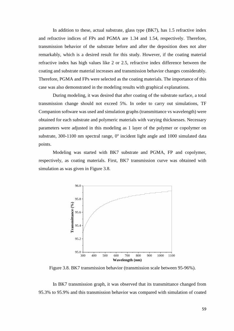
59
In addition to these, actual substrate, glass type (BK7), has 1.5 refractive index
and refractive indices of FPs and PGMA are 1.34 and 1.54, respectively. Therefore,
transmission behavior of the substrate before and after the deposition does not alter
remarkably, which is a desired result for this study. However, if the coating material
refractive index has high values like 2 or 2.5, refractive index difference between the
coating and substrate material increases and transmission behavior changes considerably.
Therefore, PGMA and FPs were selected as the coating materials. The importance of this
case was also demonstrated in the modeling results with graphical explanations.
During modeling, it was desired that after coating of the substrate surface, a total
transmission change should not exceed 5%. In order to carry out simulations, TF
Companion software was used and simulation graphs (transmittance vs wavelength) were
obtained for each substrate and polymeric materials with varying thicknesses. Necessary
parameters were adjusted in this modeling as 1 layer of the polymer or copolymer on
substrate, 300-1100 nm spectral range, 0o incident light angle and 1000 simulated data
points.
Modeling was started with BK7 substrate and PGMA, FP and copolymer,
respectively, as coating materials. First, BK7 transmission curve was obtained with
simulation as was given in Figure 3.8.
300 400 500 600 700 800 900 1000 110095.0
95.2
95.4
95.6
95.8
96.0
Tra
nsm
itta
nce
(%
)
Wavelength (nm)
Figure 3.8. BK7 transmission behavior (transmission scale between 95-96%).
In BK7 transmission graph, it was observed that its transmittance changed from
95.3% to 95.9% and this transmission behavior was compared with simulation of coated
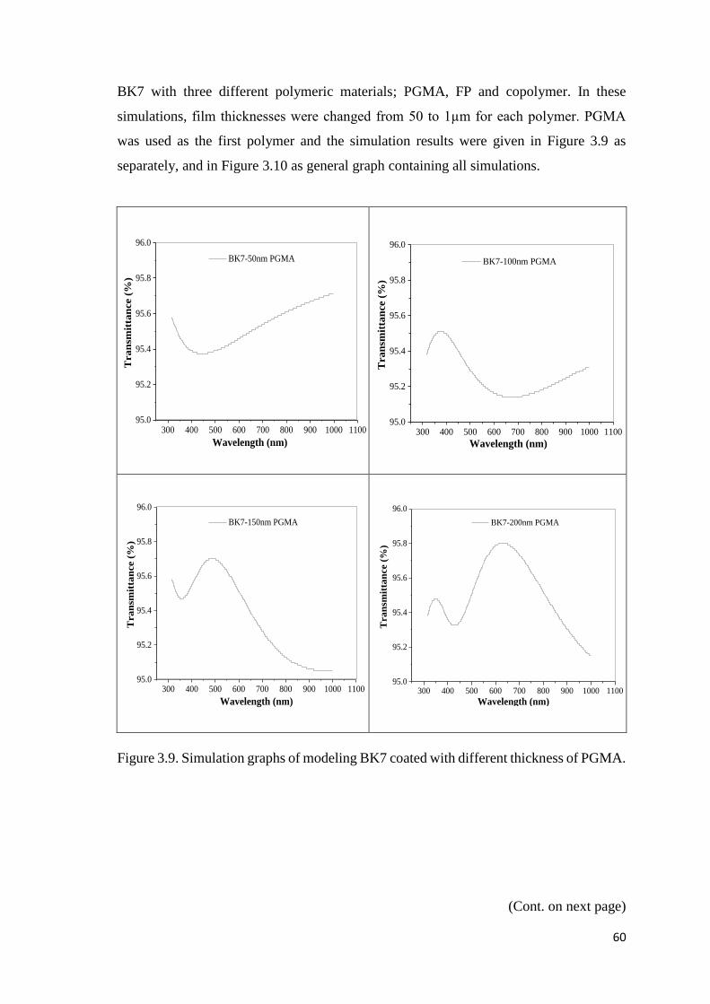
60
BK7 with three different polymeric materials; PGMA, FP and copolymer. In these
simulations, film thicknesses were changed from 50 to 1µm for each polymer. PGMA
was used as the first polymer and the simulation results were given in Figure 3.9 as
separately, and in Figure 3.10 as general graph containing all simulations.
300 400 500 600 700 800 900 1000 110095.0
95.2
95.4
95.6
95.8
96.0
Tra
nsm
itta
nce (
%)
Wavelength (nm)
BK7-50nm PGMA
300 400 500 600 700 800 900 1000 110095.0
95.2
95.4
95.6
95.8
96.0
Tran
smit
tan
ce (
%)
Wavelength (nm)
BK7-100nm PGMA
300 400 500 600 700 800 900 1000 110095.0
95.2
95.4
95.6
95.8
96.0
Tran
smit
tan
ce (
%)
Wavelength (nm)
BK7-150nm PGMA
300 400 500 600 700 800 900 1000 110095.0
95.2
95.4
95.6
95.8
96.0
Tra
nsm
itta
nce (
%)
Wavelength (nm)
BK7-200nm PGMA
Figure 3.9. Simulation graphs of modeling BK7 coated with different thickness of PGMA.
(Cont. on next page)
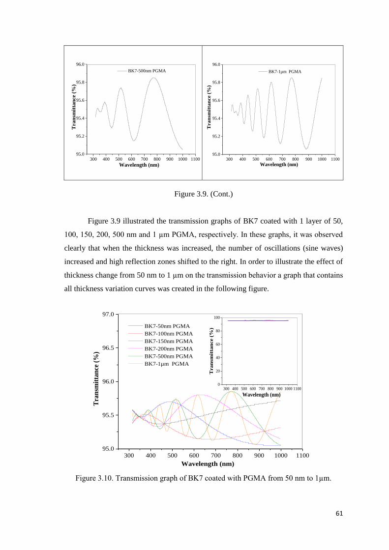
61
300 400 500 600 700 800 900 1000 110095.0
95.2
95.4
95.6
95.8
96.0
Tran
smit
tan
ce (
%)
Wavelength (nm)
BK7-500nm PGMA
300 400 500 600 700 800 900 1000 110095.0
95.2
95.4
95.6
95.8
96.0
Tran
smit
tan
ce (
%)
Wavelength (nm)
BK7-1µm PGMA
Figure 3.9. (Cont.)
Figure 3.9 illustrated the transmission graphs of BK7 coated with 1 layer of 50,
100, 150, 200, 500 nm and 1 µm PGMA, respectively. In these graphs, it was observed
clearly that when the thickness was increased, the number of oscillations (sine waves)
increased and high reflection zones shifted to the right. In order to illustrate the effect of
thickness change from 50 nm to 1 µm on the transmission behavior a graph that contains
all thickness variation curves was created in the following figure.
Figure 3.10. Transmission graph of BK7 coated with PGMA from 50 nm to 1µm.
300 400 500 600 700 800 900 1000 110095.0
95.5
96.0
96.5
97.0
Tra
nsm
itta
nce
(%
)
Wavelength (nm)
BK7-50nm PGMA
BK7-100nm PGMA
BK7-150nm PGMA
BK7-200nm PGMA
BK7-500nm PGMA
BK7-1µm PGMA
300 400 500 600 700 800 900 1000 11000
20
40
60
80
100
Tra
nsm
itta
nce (
%)
Wavelength (nm)
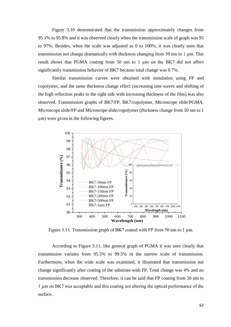
62
Figure 3.10 demonstrated that the transmission approximately changes from
95.1% to 95.8% and it was observed clearly when the transmission scale of graph was 95
to 97%. Besides, when the scale was adjusted as 0 to 100%, it was clearly seen that
transmission not change dramatically with thickness changing from 50 nm to 1 µm. This
result shows that PGMA coating from 50 nm to 1 µm on the BK7 did not affect
significantly transmission behavior of BK7 because total change was 0.7%.
Similar transmission curves were obtained with simulation using FP and
copolymer, and the same thickness change effect (increasing sine waves and shifting of
the high reflection peaks to the right side with increasing thickness of the film) was also
observed. Transmission graphs of BK7/FP, BK7/copolymer, Microscope slide/PGMA,
Microscope slide/FP and Microscope slide/copolymer (thickness change from 50 nm to 1
µm) were given in the following figures.
Figure 3.11. Transmission graph of BK7 coated with FP from 50 nm to 1 µm.
According to Figure 3.11, like general graph of PGMA it was seen clearly that
transmission variates from 95.5% to 99.5% in the narrow scale of transmission.
Furthermore, when the wide scale was examined, it illustrated that transmission not
change significantly after coating of the substrate with FP. Total change was 4% and no
transmission decrease observed. Therefore, it can be said that FP coating from 50 nm to
1 µm on BK7 was acceptable and this coating not altering the optical performance of the
surface.
300 400 500 600 700 800 900 1000 110090
91
92
93
94
95
96
97
98
99
100
Tra
nsm
itta
nce
(%
)
Wavelength (nm)
BK7-50nm FP
BK7-100nm FP
BK7-150nm FP
BK7-200nm FP
BK7-500nm FP
BK7-1µm FP 300 400 500 600 700 800 900 1000 11000
20
40
60
80
100
Tra
nsm
itta
nce (
%)
Wavelength (nm)
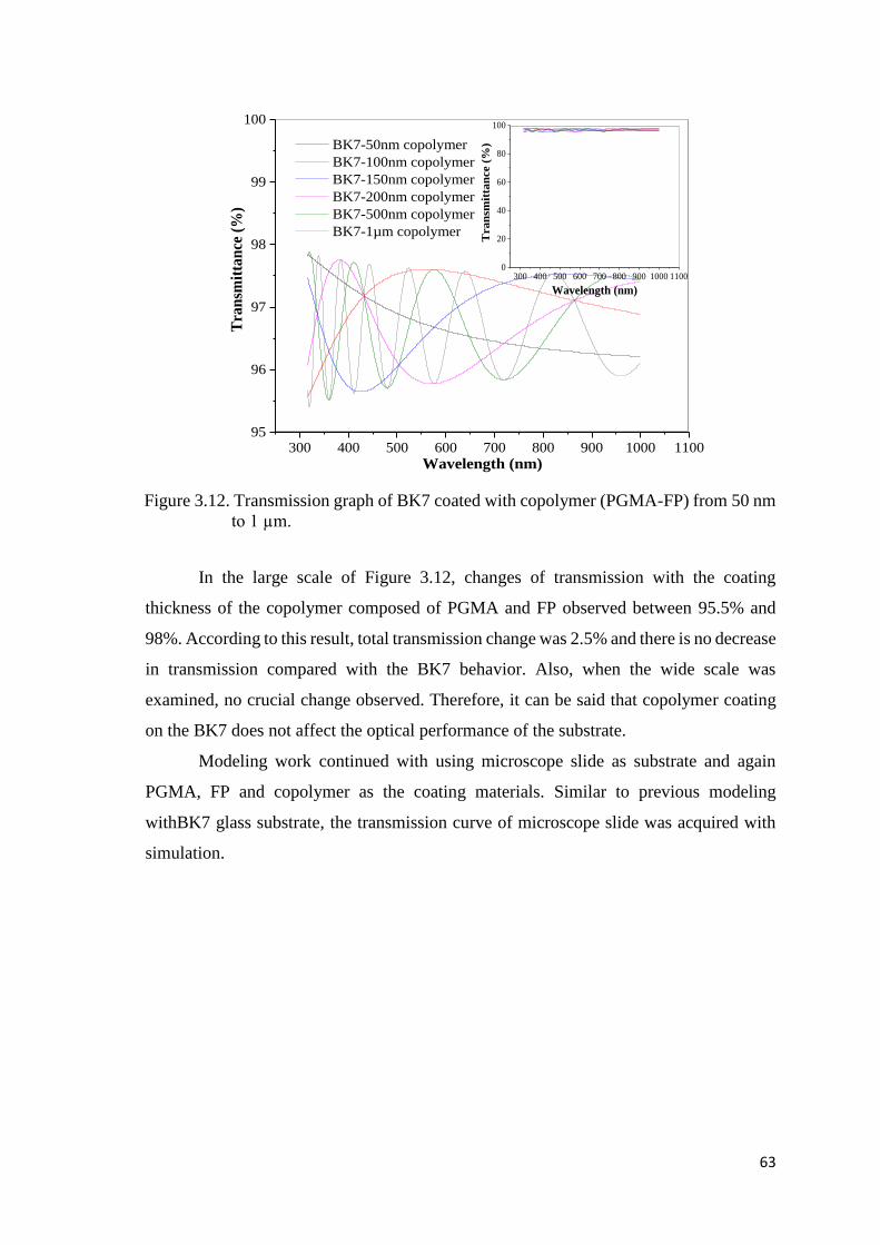
63
Figure 3.12. Transmission graph of BK7 coated with copolymer (PGMA-FP) from 50 nm
to 1 µm.
In the large scale of Figure 3.12, changes of transmission with the coating
thickness of the copolymer composed of PGMA and FP observed between 95.5% and
98%. According to this result, total transmission change was 2.5% and there is no decrease
in transmission compared with the BK7 behavior. Also, when the wide scale was
examined, no crucial change observed. Therefore, it can be said that copolymer coating
on the BK7 does not affect the optical performance of the substrate.
Modeling work continued with using microscope slide as substrate and again
PGMA, FP and copolymer as the coating materials. Similar to previous modeling
withBK7 glass substrate, the transmission curve of microscope slide was acquired with
simulation.
300 400 500 600 700 800 900 1000 110095
96
97
98
99
100
Tra
nsm
itta
nce
(%
)
Wavelength (nm)
BK7-50nm copolymer
BK7-100nm copolymer
BK7-150nm copolymer
BK7-200nm copolymer
BK7-500nm copolymer
BK7-1µm copolymer
300 400 500 600 700 800 900 1000 11000
20
40
60
80
100
Tran
smit
tan
ce (
%)
Wavelength (nm)
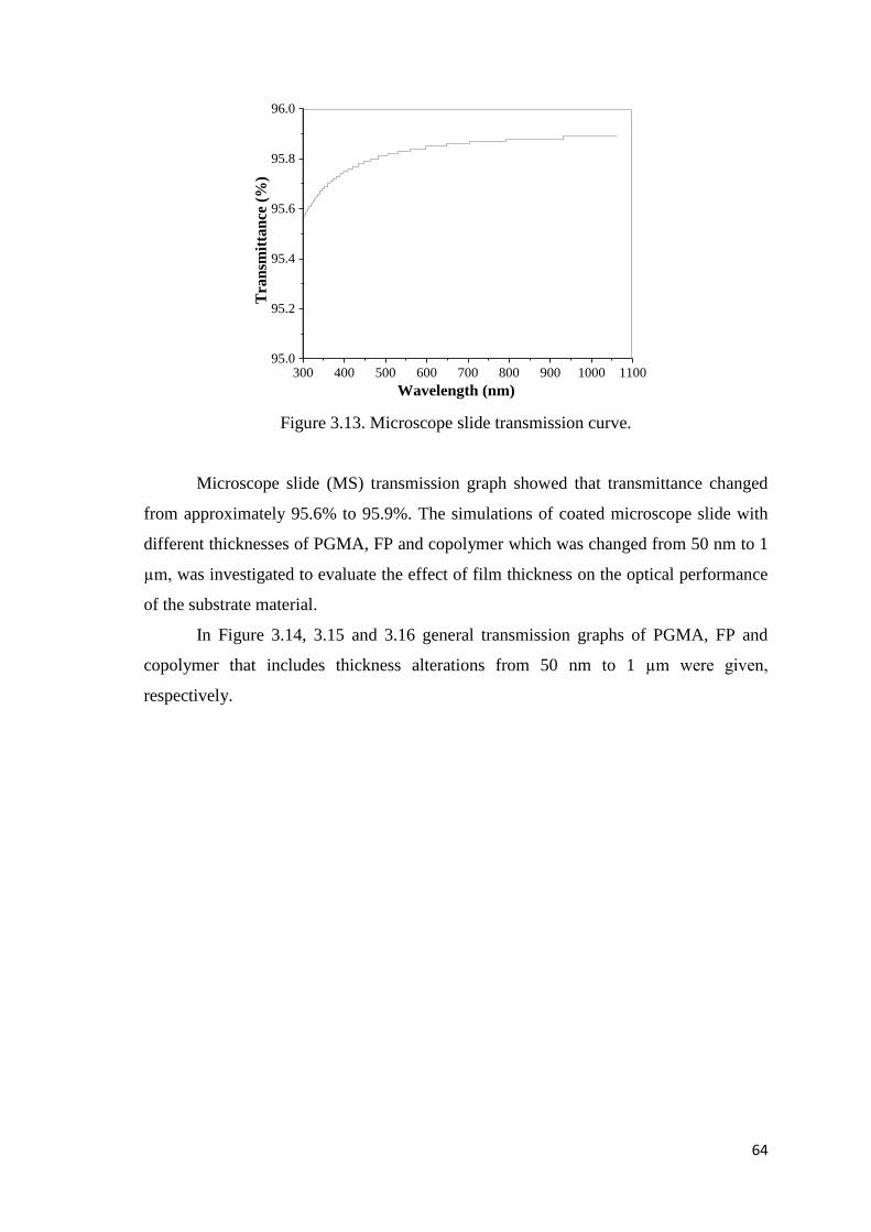
64
300 400 500 600 700 800 900 1000 110095.0
95.2
95.4
95.6
95.8
96.0
Tra
nsm
itta
nce
(%
)
Wavelength (nm)
Figure 3.13. Microscope slide transmission curve.
Microscope slide (MS) transmission graph showed that transmittance changed
from approximately 95.6% to 95.9%. The simulations of coated microscope slide with
different thicknesses of PGMA, FP and copolymer which was changed from 50 nm to 1
µm, was investigated to evaluate the effect of film thickness on the optical performance
of the substrate material.
In Figure 3.14, 3.15 and 3.16 general transmission graphs of PGMA, FP and
copolymer that includes thickness alterations from 50 nm to 1 µm were given,
respectively.
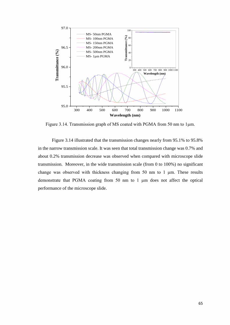
65
Figure 3.14. Transmission graph of MS coated with PGMA from 50 nm to 1µm.
Figure 3.14 illustrated that the transmission changes nearly from 95.1% to 95.8%
in the narrow transmission scale. It was seen that total transmission change was 0.7% and
about 0.2% transmission decrease was observed when compared with microscope slide
transmission. Moreover, in the wide transmission scale (from 0 to 100%) no significant
change was observed with thickness changing from 50 nm to 1 µm. These results
demonstrate that PGMA coating from 50 nm to 1 µm does not affect the optical
performance of the microscope slide.
300 400 500 600 700 800 900 1000 110095.0
95.5
96.0
96.5
97.0
Tra
nsm
itta
nce
(%
)
Wavelength (nm)
MS- 50nm PGMA
MS- 100nm PGMA
MS- 150nm PGMA
MS- 200nm PGMA
MS- 500nm PGMA
MS- 1µm PGMA
300 400 500 600 700 800 900 1000 11000
20
40
60
80
100
Tra
nsm
itta
nce (
%)
Wavelength (nm)
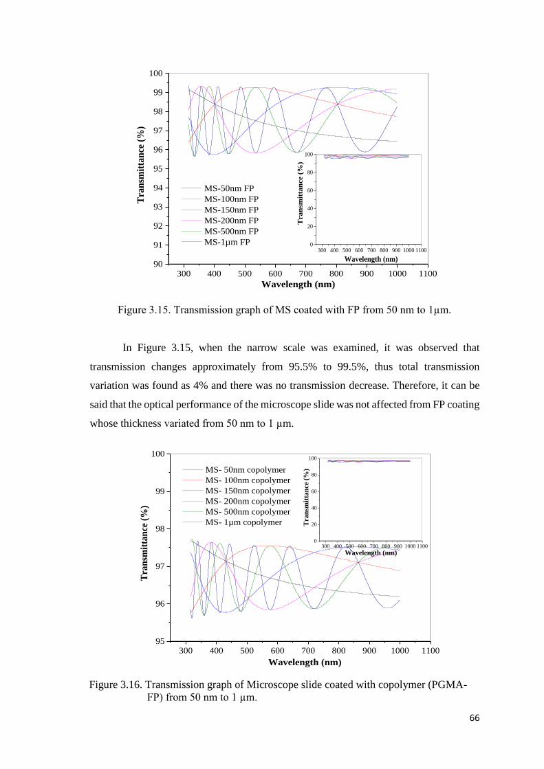
66
Figure 3.15. Transmission graph of MS coated with FP from 50 nm to 1µm.
In Figure 3.15, when the narrow scale was examined, it was observed that
transmission changes approximately from 95.5% to 99.5%, thus total transmission
variation was found as 4% and there was no transmission decrease. Therefore, it can be
said that the optical performance of the microscope slide was not affected from FP coating
whose thickness variated from 50 nm to 1 µm.
Figure 3.16. Transmission graph of Microscope slide coated with copolymer (PGMA-
FP) from 50 nm to 1 µm.
300 400 500 600 700 800 900 1000 110090
91
92
93
94
95
96
97
98
99
100
Tra
nsm
itta
nce
(%
)
Wavelength (nm)
MS-50nm FP
MS-100nm FP
MS-150nm FP
MS-200nm FP
MS-500nm FP
MS-1µm FP300 400 500 600 700 800 900 1000 1100
0
20
40
60
80
100
Tra
nsm
itta
nce (
%)
Wavelength (nm)
300 400 500 600 700 800 900 1000 110095
96
97
98
99
100
Tra
nsm
itta
nce
(%
)
Wavelength (nm)
MS- 50nm copolymer
MS- 100nm copolymer
MS- 150nm copolymer
MS- 200nm copolymer
MS- 500nm copolymer
MS- 1µm copolymer
300 400 500 600 700 800 900 1000 11000
20
40
60
80
100
Tra
nsm
itta
nce
(%
)
Wavelength (nm)
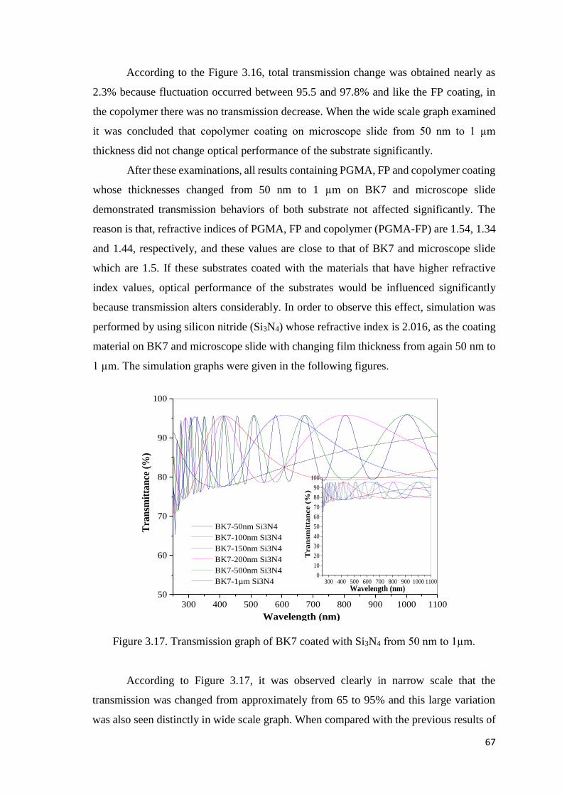
67
According to the Figure 3.16, total transmission change was obtained nearly as
2.3% because fluctuation occurred between 95.5 and 97.8% and like the FP coating, in
the copolymer there was no transmission decrease. When the wide scale graph examined
it was concluded that copolymer coating on microscope slide from 50 nm to 1 µm
thickness did not change optical performance of the substrate significantly.
After these examinations, all results containing PGMA, FP and copolymer coating
whose thicknesses changed from 50 nm to 1 µm on BK7 and microscope slide
demonstrated transmission behaviors of both substrate not affected significantly. The
reason is that, refractive indices of PGMA, FP and copolymer (PGMA-FP) are 1.54, 1.34
and 1.44, respectively, and these values are close to that of BK7 and microscope slide
which are 1.5. If these substrates coated with the materials that have higher refractive
index values, optical performance of the substrates would be influenced significantly
because transmission alters considerably. In order to observe this effect, simulation was
performed by using silicon nitride (Si3N4) whose refractive index is 2.016, as the coating
material on BK7 and microscope slide with changing film thickness from again 50 nm to
1 µm. The simulation graphs were given in the following figures.
Figure 3.17. Transmission graph of BK7 coated with Si3N4 from 50 nm to 1µm.
According to Figure 3.17, it was observed clearly in narrow scale that the
transmission was changed from approximately from 65 to 95% and this large variation
was also seen distinctly in wide scale graph. When compared with the previous results of
300 400 500 600 700 800 900 1000 110050
60
70
80
90
100
Tra
nsm
itta
nce
(%
)
Wavelength (nm)
BK7-50nm Si3N4
BK7-100nm Si3N4
BK7-150nm Si3N4
BK7-200nm Si3N4
BK7-500nm Si3N4
BK7-1µm Si3N4 300 400 500 600 700 800 900 1000 11000
10
20
30
40
50
60
70
80
90
100
Tran
smit
tan
ce (
%)
Wavelength (nm)
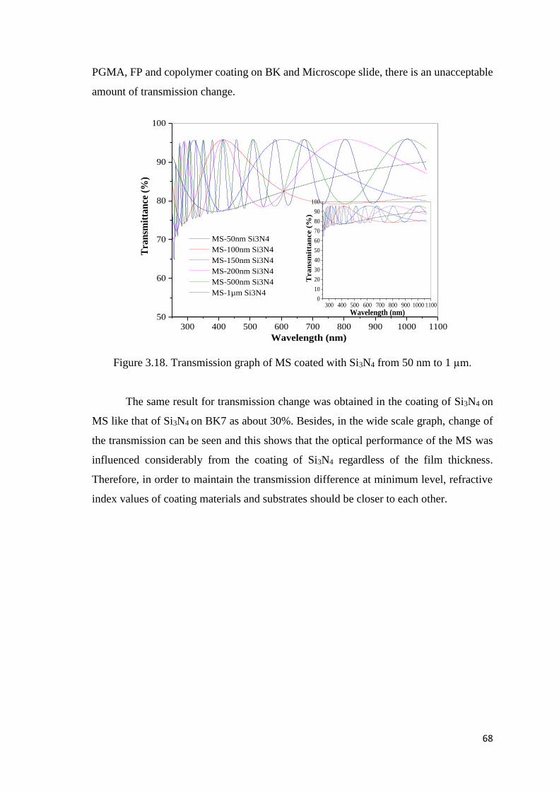
68
PGMA, FP and copolymer coating on BK and Microscope slide, there is an unacceptable
amount of transmission change.
Figure 3.18. Transmission graph of MS coated with Si3N4 from 50 nm to 1 µm.
The same result for transmission change was obtained in the coating of Si3N4 on
MS like that of Si3N4 on BK7 as about 30%. Besides, in the wide scale graph, change of
the transmission can be seen and this shows that the optical performance of the MS was
influenced considerably from the coating of Si3N4 regardless of the film thickness.
Therefore, in order to maintain the transmission difference at minimum level, refractive
index values of coating materials and substrates should be closer to each other.
300 400 500 600 700 800 900 1000 110050
60
70
80
90
100
Tra
nsm
itta
nce
(%
)
Wavelength (nm)
MS-50nm Si3N4
MS-100nm Si3N4
MS-150nm Si3N4
MS-200nm Si3N4
MS-500nm Si3N4
MS-1µm Si3N4
300 400 500 600 700 800 900 1000 11000
10
20
30
40
50
60
70
80
90
100
Tra
nsm
itta
nce (
%)
Wavelength (nm)
69
CHAPTER 4
RESULTS AND DISCUSSION
In this chapter, results of deposition experiments which include PGMA, PPFDA
and a copolymer P(GMA-PFDA) film coatings obtained using iCVD method and details
about characterization of these coatings are given.
4.1. PGMA Deposition in iCVD System
Protective nano-coating fabrication with iCVD system is one of the purposes of
this study and in order to achieve this aim. GMA was chosen as precursor owing to its
significant features, for instance, it has quite good mechanical properties due to epoxy
ring in its structure (Martin, Lau et al. 2007) as shown in Figure 4.1. Optical performance
of the substrates can be protected by deposition of PGMA because of its well enough
transparency (Bakker, Verlaan et al. 2007).
Figure 4.1. Glycidyl methacrylate (GMA) structure.
Polymeric thin film coating procedure steps in iCVD system were given explicitly
in experimental part and this procedure is pretty much the same for all coating material.
The main difference is that the deposition conditions of the materials are distinct from
each other. Thus, in this study for all PGMA, PPFDA and copolymer film depositions,
procedure explained in the experimental part was followed by using different operating
conditions such as substrate and filament temperatures, flow rate values, reactor pressure,
deposition time etc. Besides, before the starting of the depositions, operating conditions
for the PGMA, PPFDA and copolymer were determined according to the desired film
thickness based on modeling results.
70
Initially, for PGMA thin film deposition, for instance, Chan and Gleason studied
with PGMA deposition in iCVD system and they determined the general operating
conditions for this coating material and explained the effects of changing surface
temperature and monomer (GMA) partial pressure on the deposition rate and molecular
weight of polymer coated on the substrate surface (Chan and Gleason 2006). Mao and
Gleason investigated the effects of altering the filament temperature and ratio of initiator
to monomer (GMA) flow on the molecular weight of the polymer produced at the end of
the deposition (Mao and Gleason 2004). Considering these studies, operating conditions
for PGMA deposition in this study were selected in order to achieve intended thickness
of the film, and some parameters were changed with regard to the results obtained at the
end of each PGMA deposition experiments.
Before the depositions, flow calibrations were done for each coating material in
different MFCs to determine the flow rate values of monomer and initiator provided by
mass flow controllers (MFCs) to iCVD system. To decide how much flow can be
provided, GMA flow calibration was performed in MFC2 (calibrated before with GMA)
and Manual MFC (MMFC) and TBPO in both MFC1 and MFC3 (calibrated before with
nitrogen) by following the steps below:
Coating material which will be calibrated, monomer or initiator, installed to
the process channel where the related MFC is present in a stainless steels or
custom-made Pyrex-steel container.
Desired MFC count value is set on the control panel, then flow is started.
When the flow value reached the set-value, manual valve closed, chamber is
isolated and timer is started.
Pressure vs. time difference data are recorded.
From the collected pressure data, using the volume of the reactor (5572 cm3),
and reactor temperature value (298K), flow rate value (ccm) is calculated.
The same steps are repeated until at least 4 points are obtained.
The calibration results of the GMA in MFC2 and MMFC and TBPO in MFC1 and
MFC3 were given in the following figure.
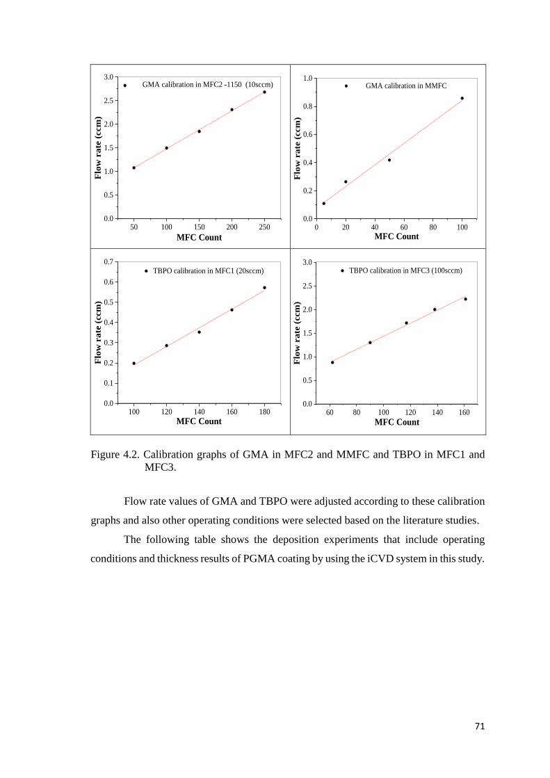
71
Figure 4.2. Calibration graphs of GMA in MFC2 and MMFC and TBPO in MFC1 and
MFC3.
Flow rate values of GMA and TBPO were adjusted according to these calibration
graphs and also other operating conditions were selected based on the literature studies.
The following table shows the deposition experiments that include operating
conditions and thickness results of PGMA coating by using the iCVD system in this study.
50 100 150 200 2500.0
0.5
1.0
1.5
2.0
2.5
3.0 GMA calibration in MFC2 -1150 (10sccm)
Flo
w r
ate
(ccm
)
MFC Count
0 20 40 60 80 1000.0
0.2
0.4
0.6
0.8
1.0 GMA calibration in MMFC
Flo
w r
ate
(ccm
)
MFC Count
100 120 140 160 1800.0
0.1
0.2
0.3
0.4
0.5
0.6
0.7TBPO calibration in MFC1 (20sccm)
Flo
w r
ate
(ccm
)
MFC Count60 80 100 120 140 160
0.0
0.5
1.0
1.5
2.0
2.5
3.0TBPO calibration in MFC3 (100sccm)
Flo
w r
ate
(ccm
)
MFC Count
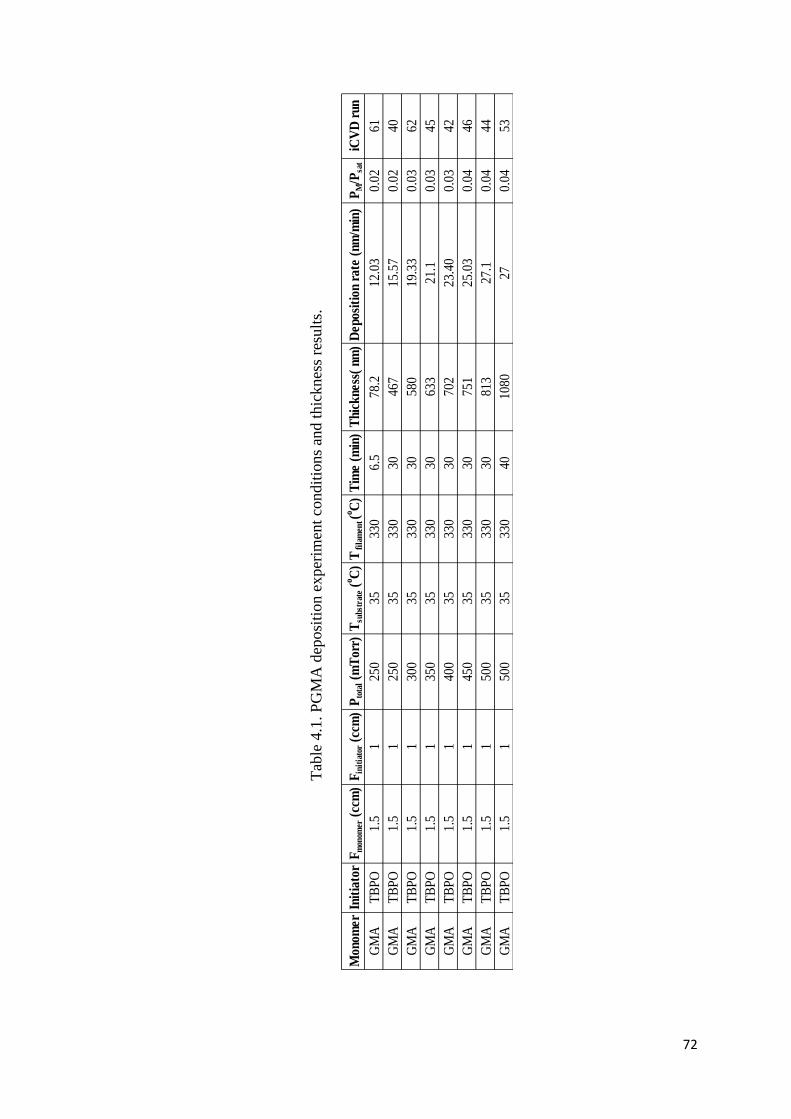
72
Tab
le 4
.1. P
GM
A d
eposi
tion e
xper
imen
t co
ndit
ions
and t
hic
knes
s re
sult
s.
Mon
omer
Init
iato
rF
mon
omer
(cc
m)
Fin
itia
tor
(ccm
)P
tota
l (m
Tor
r)T
subs
trat
e (o C
)T
fil
amen
t (o C
)T
ime
(min
)T
hick
ness
( nm
)D
epos
itio
n ra
te (
nm/m
in)
PM
/Psa
tiC
VD
run
GM
AT
BP
O1.
51
250
3533
06.
578
.212
.03
0.02
61
GM
AT
BP
O1.
51
250
3533
030
467
15.5
70.
0240
GM
AT
BP
O1.
51
300
3533
030
580
19.3
30.
0362
GM
AT
BP
O1.
51
350
3533
030
633
21.1
0.03
45
GM
AT
BP
O1.
51
400
3533
030
702
23.4
00.
0342
GM
AT
BP
O1.
51
450
3533
030
751
25.0
30.
0446
GM
AT
BP
O1.
51
500
3533
030
813
27.1
0.04
44
GM
AT
BP
O1.
51
500
3533
040
1080
270.
0453
73
In iCVD system, deposition influenced by flow ratio of initiator to monomer,
Tsubstrate, Tfilament and ratio of partial pressure to saturation pressure of monomer (PM/Psat).
Therefore, suitable values to obtain good quality film coatings were selected on literature
studies and previous experiments. For instance, the substrate temperature affects the
adsorption of monomer to the substrate surface and as a result deposition rate is also
affected. In order to improve the adsorption of monomer to the substrate surface Tsubstrate
kept lower than 50oC. However, when the temperature is decreased too much like 15 or
10oC, condensation will be observed because surface temperature also related with the
saturation pressure of the monomer. When the PM/Psat approach to unity, the excess
amount of monomer is adsorbed to the surface thus condensation occurs. At high
temperatures like 45oC, monomer adsorption is not efficient and deposition rate becomes
too low (Chan and Gleason 2006, Lau and Gleason 2006, Mittal 2013). In order to prevent
these undesired cases, Tsubstrate was chosen as 35oC which is not too low or too high, but
this temperature value is not sufficient to obtain high quality coating, hence the flow ratio
of initiator to monomer, Tfilament and PM/Psat were also need to be considered. If the value
of Finitiator/Fmonomer is very low, amount of monomer on the surface becomes high. On the
other hand, if this ratio is very high, deposition rate excessively decreases owing to the
inadequate monomer units and high amount of free radical that leads polymer chain
termination instantly (Mao and Gleason 2004, Lau and Gleason 2006). Therefore, Finitiator
was selected as 1 ccm and Fmonomer as 1.5 ccm to keep the deposition rate in average value
preventing condensation and ensuring the uniform coating. Moreover, for polymerization
reaction, free radicals in the reaction medium thus decomposition of the initiator with the
hot filaments is significant. When the temperature of the filament is high, deposition rate
increases. Additionally, Tfilament and Tsubstrate are related with each other in terms of
transferring of free radicals to the surface of the substrate (Chan and Gleason 2006, Gupta
and Gleason 2006, Lau and Gleason 2006). Thus, in this study, Tfilament was selected as
330oC.
All these conditions were kept constant in this study but only total pressure was
altered from 250 to 500 mTorr by considering PM/Psat value, to reach the desired film
thicknesses. Because, the effect of PM on deposition rate is very crucial (Lau and Gleason
2006, Mittal 2013) thus as in the Table 4.1, it was clearly observed that deposition rate
rises when the pressure increases. However, pressure value is restricted between 250 and
500 mTorr. Very low Ptotal causes low partial pressure value of monomer and initiator that
leads decreasing deposition rate. Also pressure upper limit was chosen as 500 mTorr
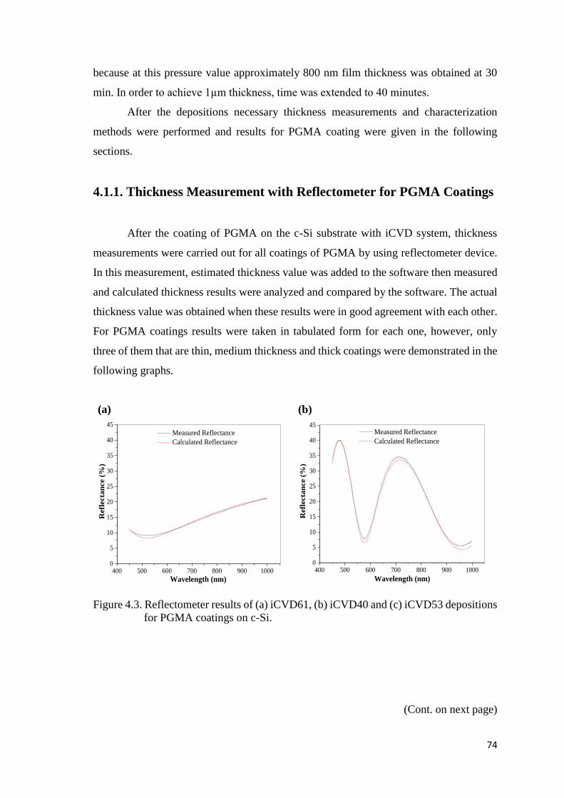
74
because at this pressure value approximately 800 nm film thickness was obtained at 30
min. In order to achieve 1µm thickness, time was extended to 40 minutes.
After the depositions necessary thickness measurements and characterization
methods were performed and results for PGMA coating were given in the following
sections.
4.1.1. Thickness Measurement with Reflectometer for PGMA Coatings
After the coating of PGMA on the c-Si substrate with iCVD system, thickness
measurements were carried out for all coatings of PGMA by using reflectometer device.
In this measurement, estimated thickness value was added to the software then measured
and calculated thickness results were analyzed and compared by the software. The actual
thickness value was obtained when these results were in good agreement with each other.
For PGMA coatings results were taken in tabulated form for each one, however, only
three of them that are thin, medium thickness and thick coatings were demonstrated in the
following graphs.
(a)
400 500 600 700 800 900 10000
5
10
15
20
25
30
35
40
45
Refl
ecta
nce (
%)
Wavelength (nm)
Measured Reflectance
Calculated Reflectance
(b)
400 500 600 700 800 900 10000
5
10
15
20
25
30
35
40
45
Refl
ecta
nce (
%)
Wavelength (nm)
Measured Reflectance
Calculated Reflectance
Figure 4.3. Reflectometer results of (a) iCVD61, (b) iCVD40 and (c) iCVD53 depositions
for PGMA coatings on c-Si.
(Cont. on next page)
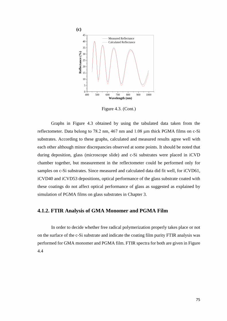
75
(c)
400 500 600 700 800 900 10000
5
10
15
20
25
30
35
40
45
Refl
ecta
nce (
%)
Wavelength (nm)
Measured Reflectance
Calculated Reflectance
Figure 4.3. (Cont.)
Graphs in Figure 4.3 obtained by using the tabulated data taken from the
reflectometer. Data belong to 78.2 nm, 467 nm and 1.08 µm thick PGMA films on c-Si
substrates. According to these graphs, calculated and measured results agree well with
each other although minor discrepancies observed at some points. It should be noted that
during deposition, glass (microscope slide) and c-Si substrates were placed in iCVD
chamber together, but measurement in the reflectometer could be performed only for
samples on c-Si substrates. Since measured and calculated data did fit well, for iCVD61,
iCVD40 and iCVD53 depositions, optical performance of the glass substrate coated with
these coatings do not affect optical performance of glass as suggested as explained by
simulation of PGMA films on glass substrates in Chapter 3.
4.1.2. FTIR Analysis of GMA Monomer and PGMA Film
In order to decide whether free radical polymerization properly takes place or not
on the surface of the c-Si substrate and indicate the coating film purity FTIR analysis was
performed for GMA monomer and PGMA film. FTIR spectra for both are given in Figure
4.4
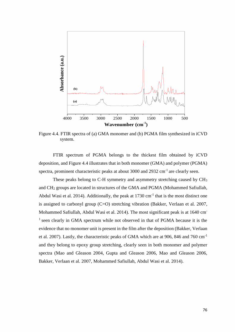
76
4000 3500 3000 2500 2000 1500 1000 500
Ab
sorb
an
ce (
a.u
.)
Wavenumber (cm-1)
(a)
(b)
Figure 4.4. FTIR spectra of (a) GMA monomer and (b) PGMA film synthesized in iCVD
system.
FTIR spectrum of PGMA belongs to the thickest film obtained by iCVD
deposition, and Figure 4.4 illustrates that in both monomer (GMA) and polymer (PGMA)
spectra, prominent characteristic peaks at about 3000 and 2932 cm-1 are clearly seen.
These peaks belong to C-H symmetry and asymmetry stretching caused by CH3
and CH2 groups are located in structures of the GMA and PGMA (Mohammed Safiullah,
Abdul Wasi et al. 2014). Additionally, the peak at 1730 cm-1 that is the most distinct one
is assigned to carbonyl group (C=O) stretching vibration (Bakker, Verlaan et al. 2007,
Mohammed Safiullah, Abdul Wasi et al. 2014). The most significant peak is at 1640 cm-
1 seen clearly in GMA spectrum while not observed in that of PGMA because it is the
evidence that no monomer unit is present in the film after the deposition (Bakker, Verlaan
et al. 2007). Lastly, the characteristic peaks of GMA which are at 906, 846 and 760 cm-1
and they belong to epoxy group stretching, clearly seen in both monomer and polymer
spectra (Mao and Gleason 2004, Gupta and Gleason 2006, Mao and Gleason 2006,
Bakker, Verlaan et al. 2007, Mohammed Safiullah, Abdul Wasi et al. 2014).
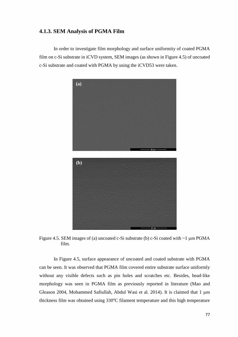
77
4.1.3. SEM Analysis of PGMA Film
In order to investigate film morphology and surface uniformity of coated PGMA
film on c-Si substrate in iCVD system, SEM images (as shown in Figure 4.5) of uncoated
c-Si substrate and coated with PGMA by using the iCVD53 were taken.
Figure 4.5. SEM images of (a) uncoated c-Si substrate (b) c-Si coated with ~1 µm PGMA
film.
In Figure 4.5, surface appearance of uncoated and coated substrate with PGMA
can be seen. It was observed that PGMA film covered entire substrate surface uniformly
without any visible defects such as pin holes and scratches etc. Besides, bead-like
morphology was seen in PGMA film as previously reported in literature (Mao and
Gleason 2004, Mohammed Safiullah, Abdul Wasi et al. 2014). It is claimed that 1 µm
thickness film was obtained using 330oC filament temperature and this high temperature
(a)
(b)
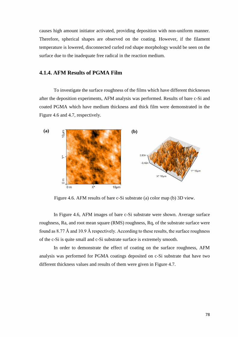
78
causes high amount initiator activated, providing deposition with non-uniform manner.
Therefore, spherical shapes are observed on the coating. However, if the filament
temperature is lowered, disconnected curled rod shape morphology would be seen on the
surface due to the inadequate free radical in the reaction medium.
4.1.4. AFM Results of PGMA Film
To investigate the surface roughness of the films which have different thicknesses
after the deposition experiments, AFM analysis was performed. Results of bare c-Si and
coated PGMA which have medium thickness and thick film were demonstrated in the
Figure 4.6 and 4.7, respectively.
Figure 4.6. AFM results of bare c-Si substrate (a) color map (b) 3D view.
In Figure 4.6, AFM images of bare c-Si substrate were shown. Average surface
roughness, Ra, and root mean square (RMS) roughness, Rq, of the substrate surface were
found as 8.77 Å and 10.9 Å respectively. According to these results, the surface roughness
of the c-Si is quite small and c-Si substrate surface is extremely smooth.
In order to demonstrate the effect of coating on the surface roughness, AFM
analysis was performed for PGMA coatings deposited on c-Si substrate that have two
different thickness values and results of them were given in Figure 4.7.
(a) (b)
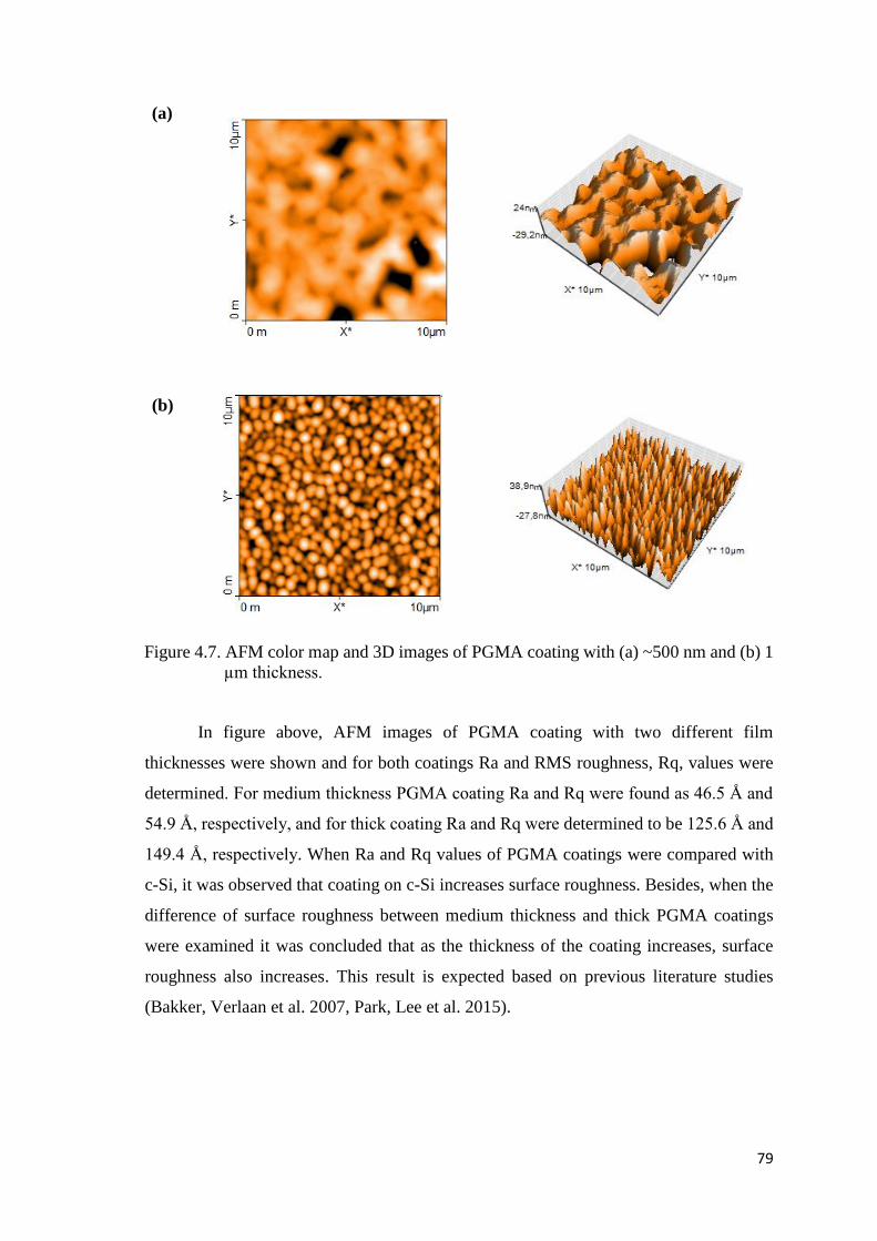
79
(a)
(b)
Figure 4.7. AFM color map and 3D images of PGMA coating with (a) ~500 nm and (b) 1
µm thickness.
In figure above, AFM images of PGMA coating with two different film
thicknesses were shown and for both coatings Ra and RMS roughness, Rq, values were
determined. For medium thickness PGMA coating Ra and Rq were found as 46.5 Å and
54.9 Å, respectively, and for thick coating Ra and Rq were determined to be 125.6 Å and
149.4 Å, respectively. When Ra and Rq values of PGMA coatings were compared with
c-Si, it was observed that coating on c-Si increases surface roughness. Besides, when the
difference of surface roughness between medium thickness and thick PGMA coatings
were examined it was concluded that as the thickness of the coating increases, surface
roughness also increases. This result is expected based on previous literature studies
(Bakker, Verlaan et al. 2007, Park, Lee et al. 2015).
m
m
m
m
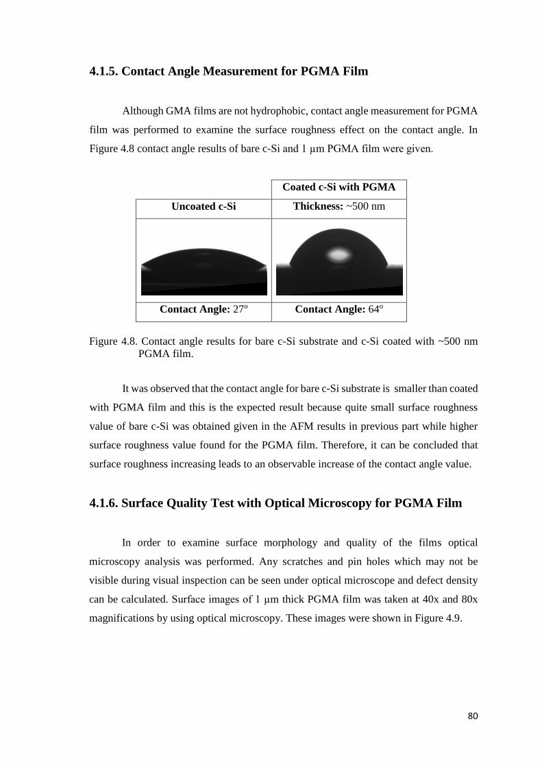
80
4.1.5. Contact Angle Measurement for PGMA Film
Although GMA films are not hydrophobic, contact angle measurement for PGMA
film was performed to examine the surface roughness effect on the contact angle. In
Figure 4.8 contact angle results of bare c-Si and 1 µm PGMA film were given.
Coated c-Si with PGMA
Uncoated c-Si Thickness: ~500 nm
Contact Angle: 27o Contact Angle: 64o
Figure 4.8. Contact angle results for bare c-Si substrate and c-Si coated with ~500 nm
PGMA film.
It was observed that the contact angle for bare c-Si substrate is smaller than coated
with PGMA film and this is the expected result because quite small surface roughness
value of bare c-Si was obtained given in the AFM results in previous part while higher
surface roughness value found for the PGMA film. Therefore, it can be concluded that
surface roughness increasing leads to an observable increase of the contact angle value.
4.1.6. Surface Quality Test with Optical Microscopy for PGMA Film
In order to examine surface morphology and quality of the films optical
microscopy analysis was performed. Any scratches and pin holes which may not be
visible during visual inspection can be seen under optical microscope and defect density
can be calculated. Surface images of 1 µm thick PGMA film was taken at 40x and 80x
magnifications by using optical microscopy. These images were shown in Figure 4.9.
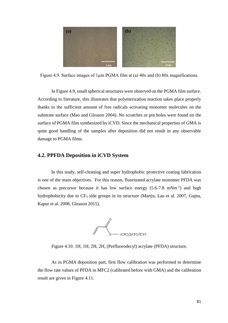
81
Figure 4.9. Surface images of 1µm PGMA film at (a) 40x and (b) 80x magnifications.
In Figure 4.9, small spherical structures were observed on the PGMA film surface.
According to literature, this illustrates that polymerization reaction takes place properly
thanks to the sufficient amount of free radicals activating monomer molecules on the
substrate surface (Mao and Gleason 2004). No scratches or pin holes were found on the
surface of PGMA film synthesized by iCVD. Since the mechanical properties of GMA is
quite good handling of the samples after deposition did not result in any observable
damage to PGMA films.
4.2. PPFDA Deposition in iCVD System
In this study, self-cleaning and super hydrophobic protective coating fabrication
is one of the main objectives. For this reason, fluorinated acrylate monomer PFDA was
chosen as precursor because it has low surface energy (5.6-7.8 mNm-1) and high
hydrophobicity due to CF3 side groups in its structure (Martin, Lau et al. 2007, Gupta,
Kapur et al. 2008, Gleason 2015).
Figure 4.10. 1H, 1H, 2H, 2H, (Perfluorodecyl) acrylate (PFDA) structure.
As in PGMA deposition part, first flow calibration was performed to determine
the flow rate values of PFDA in MFC2 (calibrated before with GMA) and the calibration
result are given in Figure 4.11.
(a) (b)
4 µm 2 µm
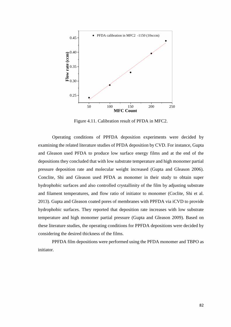
82
50 100 150 200 250
0.25
0.30
0.35
0.40
0.45PFDA calibration in MFC2 -1150 (10sccm)
Flo
w r
ate
(cc
m)
MFC Count
Figure 4.11. Calibration result of PFDA in MFC2.
Operating conditions of PPFDA deposition experiments were decided by
examining the related literature studies of PFDA deposition by CVD. For instance, Gupta
and Gleason used PFDA to produce low surface energy films and at the end of the
depositions they concluded that with low substrate temperature and high monomer partial
pressure deposition rate and molecular weight increased (Gupta and Gleason 2006).
Conclite, Shi and Gleason used PFDA as monomer in their study to obtain super
hydrophobic surfaces and also controlled crystallinity of the film by adjusting substrate
and filament temperatures, and flow ratio of initiator to monomer (Coclite, Shi et al.
2013). Gupta and Gleason coated pores of membranes with PPFDA via iCVD to provide
hydrophobic surfaces. They reported that deposition rate increases with low substrate
temperature and high monomer partial pressure (Gupta and Gleason 2009). Based on
these literature studies, the operating conditions for PPFDA depositions were decided by
considering the desired thickness of the films.
PPFDA film depositions were performed using the PFDA monomer and TBPO as
initiator.
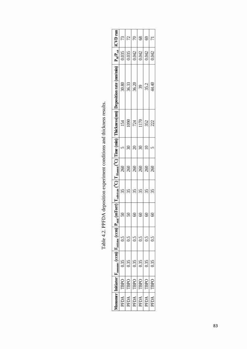
83
Tab
le 4
.2. P
PF
DA
dep
osi
tion e
xper
imen
t co
ndit
ions
and t
hic
knes
s re
sult
s.
Mon
omer
Init
iato
rF
mon
omer
(cc
m)
Fin
itia
tor
(ccm
)P
tota
l (m
Tor
r)T
subs
trat
e (o C
)T
fil
amen
t (o C
)T
ime
(min
)T
hick
ness
(nm
)D
epos
itio
n ra
te (
nm/m
in)
PM
/Psa
tiC
VD
run
PF
DA
TB
PO
0.35
0.5
5035
260
515
430
.80
0.03
573
PF
DA
TB
PO
0.35
0.5
5035
260
3010
9036
.33
0.03
572
PF
DA
TB
PO
0.35
0.5
6035
260
2072
436
.20
0.04
270
PF
DA
TB
PO
0.35
0.5
6035
260
3011
7039
0.04
268
PF
DA
TB
PO
0.35
0.5
6035
260
1035
235
.20.
042
69
PF
DA
TB
PO
0.35
0.5
6035
260
522
244
.40
0.04
271
84
In PGMA deposition part, effects of operating parameters such as Tsubstrate, Tfilament,
initiator to monomer flow ratio and PM/Psat were explained briefly. Considering the
influence of these parameters, operating conditions were set carefully. For example,
Gupta and Gleason changed the initiator to monomer flow ratio from 1.22 to 6.3 and
results showed that when the ratio increased deposition rate decreased (Gupta and Gleason
2006). Also, Gupta, Kapur et al. used the initiator to monomer ratio became 2.3 for their
study (Gupta, Kapur et al. 2008). Based on these studies, monomer and initiator flow
rates were selected as 0.35 and 0.5 ccm for PPFDA to prevent monomer condensation and
non-uniform coating. Substrate temperature, Tsubstrate was set to 35oC as for PGMA
depositions because this temperature is the suitable for the adsorption of the monomer
and free radical on the substrate surface effectively. Total pressure of the system was set
to between 50 and 60 mTorr. However, when the pressure increased further, monomer
condensation was observed. At lower pressures deposition rate decreased to unacceptable
levels. In order to achieve desired thickness values, Tfilament was set to 260oC. At the end
of the depositions, thickness measurements were performed by reflectometer before other
characterization tools were applied.
4.2.1. Thickness Measurement with Reflectometer for PPFDA Coatings
For all PPFDA coatings, thickness measurement were performed using
reflectometer, but only thin (~100 nm), medium (~500 nm) and thick (~1 µm) coating
results were illustrated in Figure 4.12 below.
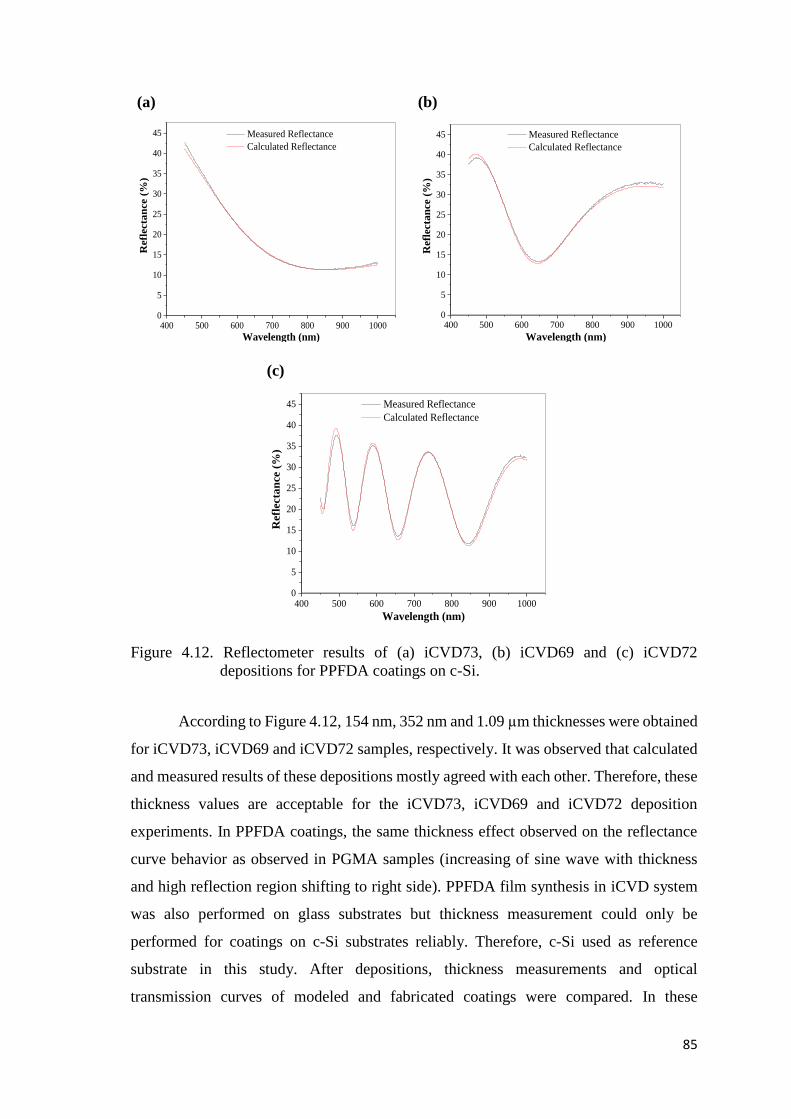
85
(a)
400 500 600 700 800 900 10000
5
10
15
20
25
30
35
40
45R
efl
ecta
nce (
%)
Wavelength (nm)
Measured Reflectance
Calculated Reflectance
(b)
400 500 600 700 800 900 10000
5
10
15
20
25
30
35
40
45
Refl
ecta
nce (
%)
Wavelength (nm)
Measured Reflectance
Calculated Reflectance
(c)
400 500 600 700 800 900 10000
5
10
15
20
25
30
35
40
45
Refl
ecta
nce (
%)
Wavelength (nm)
Measured Reflectance
Calculated Reflectance
Figure 4.12. Reflectometer results of (a) iCVD73, (b) iCVD69 and (c) iCVD72
depositions for PPFDA coatings on c-Si.
According to Figure 4.12, 154 nm, 352 nm and 1.09 µm thicknesses were obtained
for iCVD73, iCVD69 and iCVD72 samples, respectively. It was observed that calculated
and measured results of these depositions mostly agreed with each other. Therefore, these
thickness values are acceptable for the iCVD73, iCVD69 and iCVD72 deposition
experiments. In PPFDA coatings, the same thickness effect observed on the reflectance
curve behavior as observed in PGMA samples (increasing of sine wave with thickness
and high reflection region shifting to right side). PPFDA film synthesis in iCVD system
was also performed on glass substrates but thickness measurement could only be
performed for coatings on c-Si substrates reliably. Therefore, c-Si used as reference
substrate in this study. After depositions, thickness measurements and optical
transmission curves of modeled and fabricated coatings were compared. In these
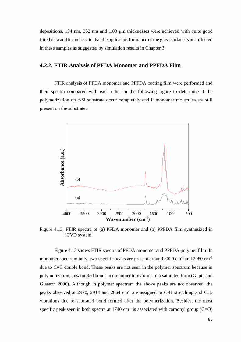
86
depositions, 154 nm, 352 nm and 1.09 µm thicknesses were achieved with quite good
fitted data and it can be said that the optical performance of the glass surface is not affected
in these samples as suggested by simulation results in Chapter 3.
4.2.2. FTIR Analysis of PFDA Monomer and PPFDA Film
FTIR analysis of PFDA monomer and PPFDA coating film were performed and
their spectra compared with each other in the following figure to determine if the
polymerization on c-Si substrate occur completely and if monomer molecules are still
present on the substrate.
4000 3500 3000 2500 2000 1500 1000 500
Ab
sorb
an
ce (
a.u
.)
Wavenumber (cm-1
)
(a)
(b)
Figure 4.13. FTIR spectra of (a) PFDA monomer and (b) PPFDA film synthesized in
iCVD system.
Figure 4.13 shows FTIR spectra of PFDA monomer and PPFDA polymer film. In
monomer spectrum only, two specific peaks are present around 3020 cm-1 and 2980 cm-1
due to C=C double bond. These peaks are not seen in the polymer spectrum because in
polymerization, unsaturated bonds in monomer transforms into saturated form (Gupta and
Gleason 2006). Although in polymer spectrum the above peaks are not observed, the
peaks observed at 2970, 2914 and 2864 cm-1 are assigned to C-H stretching and CH2
vibrations due to saturated bond formed after the polymerization. Besides, the most
specific peak seen in both spectra at 1740 cm-1 is associated with carbonyl group (C=O)
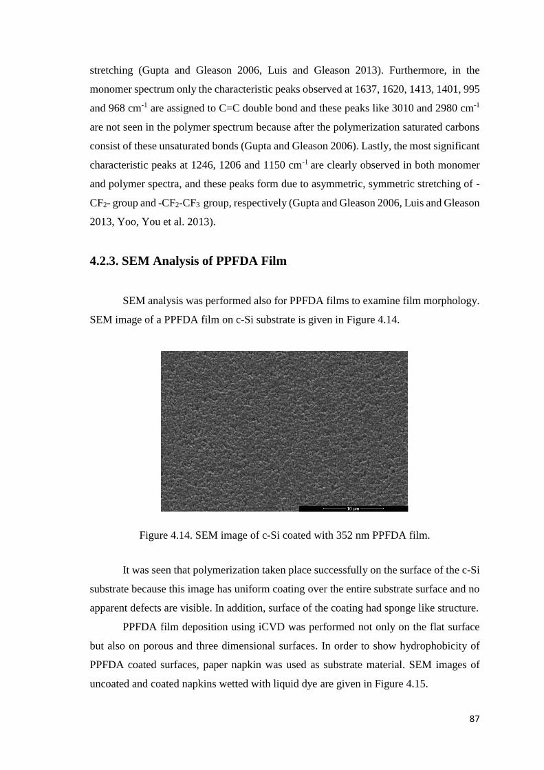
87
stretching (Gupta and Gleason 2006, Luis and Gleason 2013). Furthermore, in the
monomer spectrum only the characteristic peaks observed at 1637, 1620, 1413, 1401, 995
and 968 cm-1 are assigned to C=C double bond and these peaks like 3010 and 2980 cm-1
are not seen in the polymer spectrum because after the polymerization saturated carbons
consist of these unsaturated bonds (Gupta and Gleason 2006). Lastly, the most significant
characteristic peaks at 1246, 1206 and 1150 cm-1 are clearly observed in both monomer
and polymer spectra, and these peaks form due to asymmetric, symmetric stretching of -
CF2- group and -CF2-CF3 group, respectively (Gupta and Gleason 2006, Luis and Gleason
2013, Yoo, You et al. 2013).
4.2.3. SEM Analysis of PPFDA Film
SEM analysis was performed also for PPFDA films to examine film morphology.
SEM image of a PPFDA film on c-Si substrate is given in Figure 4.14.
Figure 4.14. SEM image of c-Si coated with 352 nm PPFDA film.
It was seen that polymerization taken place successfully on the surface of the c-Si
substrate because this image has uniform coating over the entire substrate surface and no
apparent defects are visible. In addition, surface of the coating had sponge like structure.
PPFDA film deposition using iCVD was performed not only on the flat surface
but also on porous and three dimensional surfaces. In order to show hydrophobicity of
PPFDA coated surfaces, paper napkin was used as substrate material. SEM images of
uncoated and coated napkins wetted with liquid dye are given in Figure 4.15.
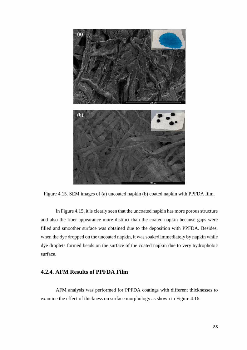
88
Figure 4.15. SEM images of (a) uncoated napkin (b) coated napkin with PPFDA film.
In Figure 4.15, it is clearly seen that the uncoated napkin has more porous structure
and also the fiber appearance more distinct than the coated napkin because gaps were
filled and smoother surface was obtained due to the deposition with PPFDA. Besides,
when the dye dropped on the uncoated napkin, it was soaked immediately by napkin while
dye droplets formed beads on the surface of the coated napkin due to very hydrophobic
surface.
4.2.4. AFM Results of PPFDA Film
AFM analysis was performed for PPFDA coatings with different thicknesses to
examine the effect of thickness on surface morphology as shown in Figure 4.16.
(a)
(b)
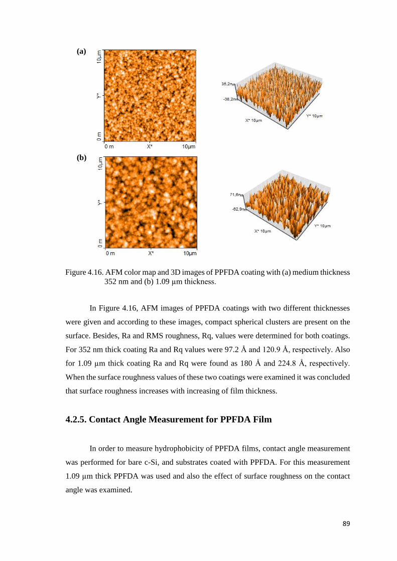
89
(a)
(b)
Figure 4.16. AFM color map and 3D images of PPFDA coating with (a) medium thickness
352 nm and (b) 1.09 µm thickness.
In Figure 4.16, AFM images of PPFDA coatings with two different thicknesses
were given and according to these images, compact spherical clusters are present on the
surface. Besides, Ra and RMS roughness, Rq, values were determined for both coatings.
For 352 nm thick coating Ra and Rq values were 97.2 Å and 120.9 Å, respectively. Also
for 1.09 µm thick coating Ra and Rq were found as 180 Å and 224.8 Å, respectively.
When the surface roughness values of these two coatings were examined it was concluded
that surface roughness increases with increasing of film thickness.
4.2.5. Contact Angle Measurement for PPFDA Film
In order to measure hydrophobicity of PPFDA films, contact angle measurement
was performed for bare c-Si, and substrates coated with PPFDA. For this measurement
1.09 µm thick PPFDA was used and also the effect of surface roughness on the contact
angle was examined.
m
m
m
m
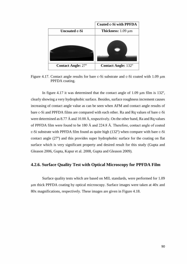
90
Coated c-Si with PPFDA
Uncoated c-Si Thickness: 1.09 µm
Contact Angle: 27o Contact Angle: 132o
Figure 4.17. Contact angle results for bare c-Si substrate and c-Si coated with 1.09 µm
PPFDA coating.
In figure 4.17 it was determined that the contact angle of 1.09 µm film is 132o,
clearly showing a very hydrophobic surface. Besides, surface roughness increment causes
increasing of contact angle value as can be seen when AFM and contact angle results of
bare c-Si and PPFDA films are compared with each other. Ra and Rq values of bare c-Si
were determined as 8.77 Å and 10.88 Å, respectively. On the other hand, Ra and Rq values
of PPFDA film were found to be 180 Å and 224.8 Å. Therefore, contact angle of coated
c-Si substrate with PPFDA film found as quite high (132o) when compare with bare c-Si
contact angle (27o) and this provides super hydrophobic surface for the coating on flat
surface which is very significant property and desired result for this study (Gupta and
Gleason 2006, Gupta, Kapur et al. 2008, Gupta and Gleason 2009).
4.2.6. Surface Quality Test with Optical Microscopy for PPFDA Film
Surface quality tests which are based on MIL standards, were performed for 1.09
µm thick PPFDA coating by optical microscopy. Surface images were taken at 40x and
80x magnifications, respectively. These images are given in Figure 4.18.
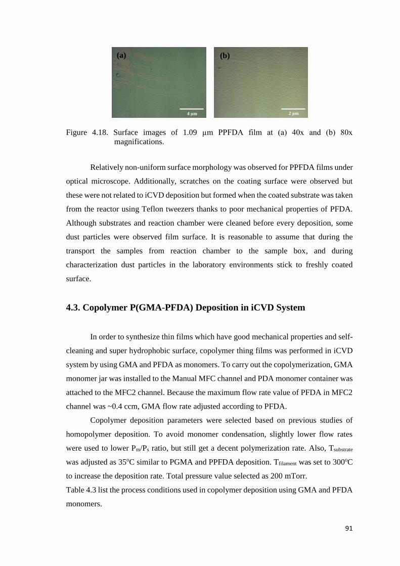
91
Figure 4.18. Surface images of 1.09 µm PPFDA film at (a) 40x and (b) 80x
magnifications.
Relatively non-uniform surface morphology was observed for PPFDA films under
optical microscope. Additionally, scratches on the coating surface were observed but
these were not related to iCVD deposition but formed when the coated substrate was taken
from the reactor using Teflon tweezers thanks to poor mechanical properties of PFDA.
Although substrates and reaction chamber were cleaned before every deposition, some
dust particles were observed film surface. It is reasonable to assume that during the
transport the samples from reaction chamber to the sample box, and during
characterization dust particles in the laboratory environments stick to freshly coated
surface.
4.3. Copolymer P(GMA-PFDA) Deposition in iCVD System
In order to synthesize thin films which have good mechanical properties and self-
cleaning and super hydrophobic surface, copolymer thing films was performed in iCVD
system by using GMA and PFDA as monomers. To carry out the copolymerization, GMA
monomer jar was installed to the Manual MFC channel and PDA monomer container was
attached to the MFC2 channel. Because the maximum flow rate value of PFDA in MFC2
channel was ~0.4 ccm, GMA flow rate adjusted according to PFDA.
Copolymer deposition parameters were selected based on previous studies of
homopolymer deposition. To avoid monomer condensation, slightly lower flow rates
were used to lower Pm/Ps ratio, but still get a decent polymerization rate. Also, Tsubstrate
was adjusted as 35oC similar to PGMA and PPFDA deposition. Tfilament was set to 300oC
to increase the deposition rate. Total pressure value selected as 200 mTorr.
Table 4.3 list the process conditions used in copolymer deposition using GMA and PFDA
monomers.
(a)
4 µm
(b)
2 µm
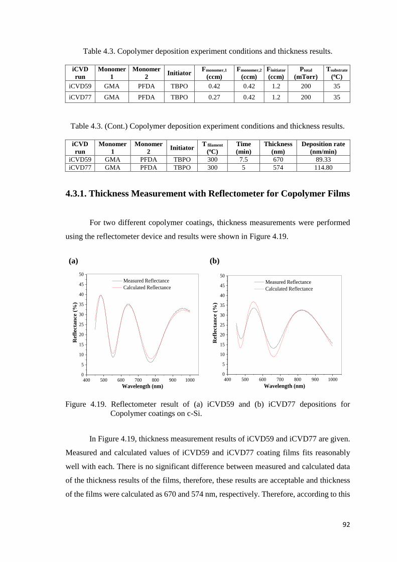
92
Table 4.3. Copolymer deposition experiment conditions and thickness results.
iCVD
run
Monomer
1
Monomer
2 Initiator
Fmonomer,1
(ccm)
Fmonomer,2
(ccm)
Finitiator
(ccm)
Ptotal
(mTorr)
Tsubstrate
(oC)
iCVD59 GMA PFDA TBPO 0.42 0.42 1.2 200 35
iCVD77 GMA PFDA TBPO 0.27 0.42 1.2 200 35
Table 4.3. (Cont.) Copolymer deposition experiment conditions and thickness results.
iCVD
run
Monomer
1
Monomer
2 Initiator
T filament
(oC)
Time
(min)
Thickness
(nm)
Deposition rate
(nm/min)
iCVD59 GMA PFDA TBPO 300 7.5 670 89.33
iCVD77 GMA PFDA TBPO 300 5 574 114.80
4.3.1. Thickness Measurement with Reflectometer for Copolymer Films
For two different copolymer coatings, thickness measurements were performed
using the reflectometer device and results were shown in Figure 4.19.
(a)
400 500 600 700 800 900 10000
5
10
15
20
25
30
35
40
45
50
Refl
ecta
nce (
%)
Wavelength (nm)
Measured Reflectance
Calculated Reflectance
(b)
400 500 600 700 800 900 10000
5
10
15
20
25
30
35
40
45
50
Refl
ecta
nce (
%)
Wavelength (nm)
Measured Reflectance
Calculated Reflectance
Figure 4.19. Reflectometer result of (a) iCVD59 and (b) iCVD77 depositions for
Copolymer coatings on c-Si.
In Figure 4.19, thickness measurement results of iCVD59 and iCVD77 are given.
Measured and calculated values of iCVD59 and iCVD77 coating films fits reasonably
well with each. There is no significant difference between measured and calculated data
of the thickness results of the films, therefore, these results are acceptable and thickness
of the films were calculated as 670 and 574 nm, respectively. Therefore, according to this
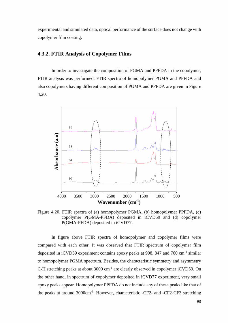
93
experimental and simulated data, optical performance of the surface does not change with
copolymer film coating.
4.3.2. FTIR Analysis of Copolymer Films
In order to investigate the composition of PGMA and PPFDA in the copolymer,
FTIR analysis was performed. FTIR spectra of homopolymer PGMA and PPFDA and
also copolymers having different composition of PGMA and PPFDA are given in Figure
4.20.
4000 3500 3000 2500 2000 1500 1000 500
Ab
sorb
an
ce (
a.u
)
Wavenumber (cm-1)
(a)
(b)
(c)
(d)
Figure 4.20. FTIR spectra of (a) homopolymer PGMA, (b) homopolymer PPFDA, (c)
copolymer P(GMA-PFDA) deposited in iCVD59 and (d) copolymer
P(GMA-PFDA) deposited in iCVD77.
In figure above FTIR spectra of homopolymer and copolymer films were
compared with each other. It was observed that FTIR spectrum of copolymer film
deposited in iCVD59 experiment contains epoxy peaks at 908, 847 and 760 cm-1 similar
to homopolymer PGMA spectrum. Besides, the characteristic symmetry and asymmetry
C-H stretching peaks at about 3000 cm-1 are clearly observed in copolymer iCVD59. On
the other hand, in spectrum of copolymer deposited in iCVD77 experiment, very small
epoxy peaks appear. Homopolymer PPFDA do not include any of these peaks like that of
the peaks at around 3000cm-1. However, characteristic -CF2- and -CF2-CF3 stretching
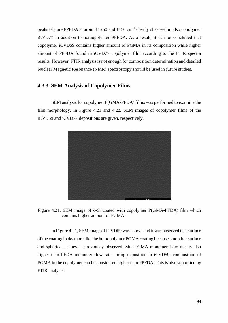
94
peaks of pure PPFDA at around 1250 and 1150 cm-1 clearly observed in also copolymer
iCVD77 in addition to homopolymer PPFDA. As a result, it can be concluded that
copolymer iCVD59 contains higher amount of PGMA in its composition while higher
amount of PPFDA found in iCVD77 copolymer film according to the FTIR spectra
results. However, FTIR analysis is not enough for composition determination and detailed
Nuclear Magnetic Resonance (NMR) spectroscopy should be used in future studies.
4.3.3. SEM Analysis of Copolymer Films
SEM analysis for copolymer P(GMA-PFDA) films was performed to examine the
film morphology. In Figure 4.21 and 4.22, SEM images of copolymer films of the
iCVD59 and iCVD77 depositions are given, respectively.
Figure 4.21. SEM image of c-Si coated with copolymer P(GMA-PFDA) film which
contains higher amount of PGMA.
In Figure 4.21, SEM image of iCVD59 was shown and it was observed that surface
of the coating looks more like the homopolymer PGMA coating because smoother surface
and spherical shapes as previously observed. Since GMA monomer flow rate is also
higher than PFDA monomer flow rate during deposition in iCVD59, composition of
PGMA in the copolymer can be considered higher than PPFDA. This is also supported by
FTIR analysis.
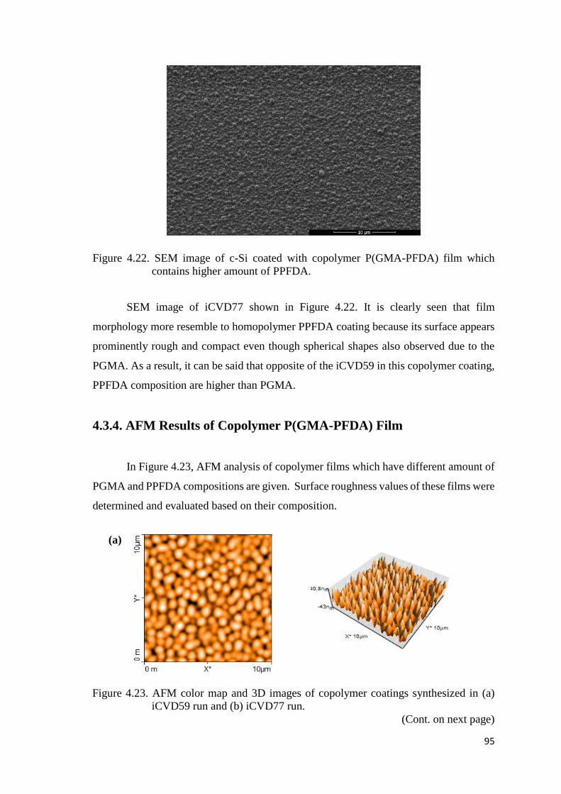
95
Figure 4.22. SEM image of c-Si coated with copolymer P(GMA-PFDA) film which
contains higher amount of PPFDA.
SEM image of iCVD77 shown in Figure 4.22. It is clearly seen that film
morphology more resemble to homopolymer PPFDA coating because its surface appears
prominently rough and compact even though spherical shapes also observed due to the
PGMA. As a result, it can be said that opposite of the iCVD59 in this copolymer coating,
PPFDA composition are higher than PGMA.
4.3.4. AFM Results of Copolymer P(GMA-PFDA) Film
In Figure 4.23, AFM analysis of copolymer films which have different amount of
PGMA and PPFDA compositions are given. Surface roughness values of these films were
determined and evaluated based on their composition.
(a)
Figure 4.23. AFM color map and 3D images of copolymer coatings synthesized in (a)
iCVD59 run and (b) iCVD77 run.
(Cont. on next page)
m
m
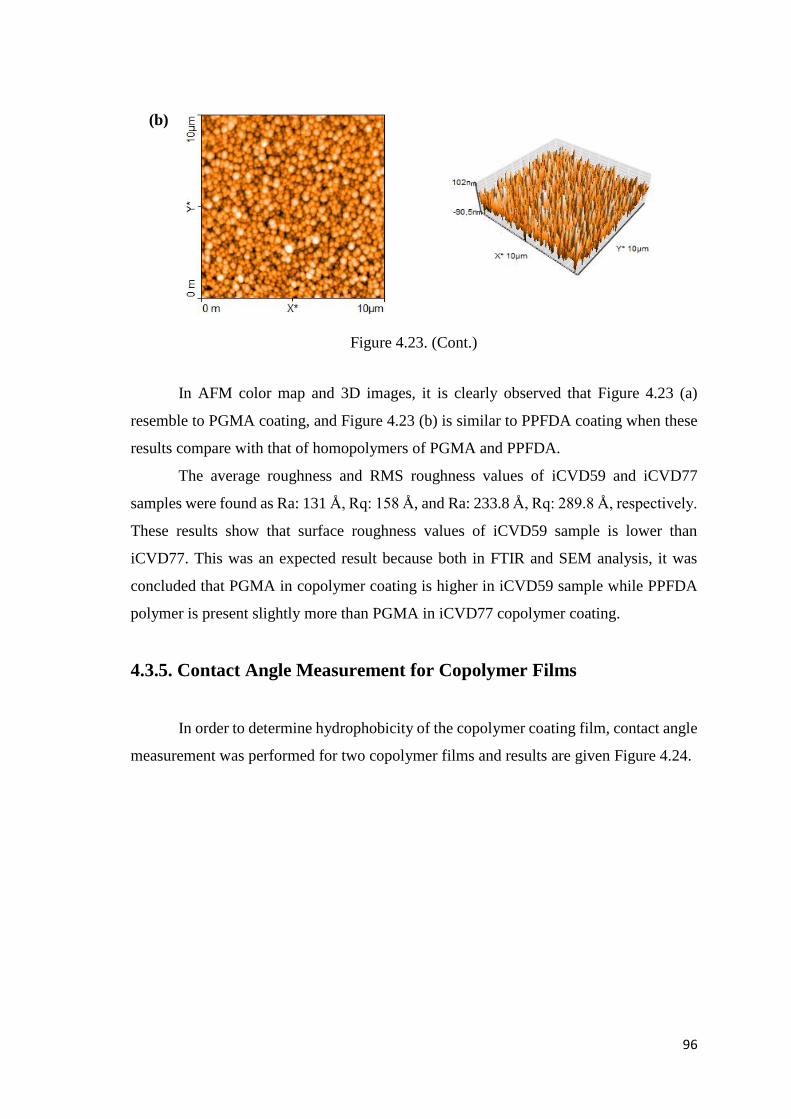
96
(b)
Figure 4.23. (Cont.)
In AFM color map and 3D images, it is clearly observed that Figure 4.23 (a)
resemble to PGMA coating, and Figure 4.23 (b) is similar to PPFDA coating when these
results compare with that of homopolymers of PGMA and PPFDA.
The average roughness and RMS roughness values of iCVD59 and iCVD77
samples were found as Ra: 131 Å, Rq: 158 Å, and Ra: 233.8 Å, Rq: 289.8 Å, respectively.
These results show that surface roughness values of iCVD59 sample is lower than
iCVD77. This was an expected result because both in FTIR and SEM analysis, it was
concluded that PGMA in copolymer coating is higher in iCVD59 sample while PPFDA
polymer is present slightly more than PGMA in iCVD77 copolymer coating.
4.3.5. Contact Angle Measurement for Copolymer Films
In order to determine hydrophobicity of the copolymer coating film, contact angle
measurement was performed for two copolymer films and results are given Figure 4.24.
m
m
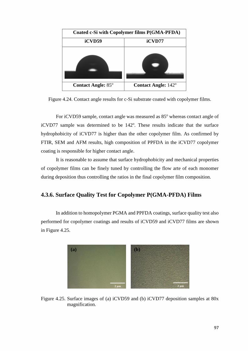
97
Coated c-Si with Copolymer films P(GMA-PFDA)
iCVD59 iCVD77
Contact Angle: 85o Contact Angle: 142o
Figure 4.24. Contact angle results for c-Si substrate coated with copolymer films.
For iCVD59 sample, contact angle was measured as 85o whereas contact angle of
iCVD77 sample was determined to be 142o. These results indicate that the surface
hydrophobicity of iCVD77 is higher than the other copolymer film. As confirmed by
FTIR, SEM and AFM results, high composition of PPFDA in the iCVD77 copolymer
coating is responsible for higher contact angle.
It is reasonable to assume that surface hydrophobicity and mechanical properties
of copolymer films can be finely tuned by controlling the flow arte of each monomer
during deposition thus controlling the ratios in the final copolymer film composition.
4.3.6. Surface Quality Test for Copolymer P(GMA-PFDA) Films
In addition to homopolymer PGMA and PPFDA coatings, surface quality test also
performed for copolymer coatings and results of iCVD59 and iCVD77 films are shown
in Figure 4.25.
Figure 4.25. Surface images of (a) iCVD59 and (b) iCVD77 deposition samples at 80x
magnification.
(a) (b)
2 µm 2 µm
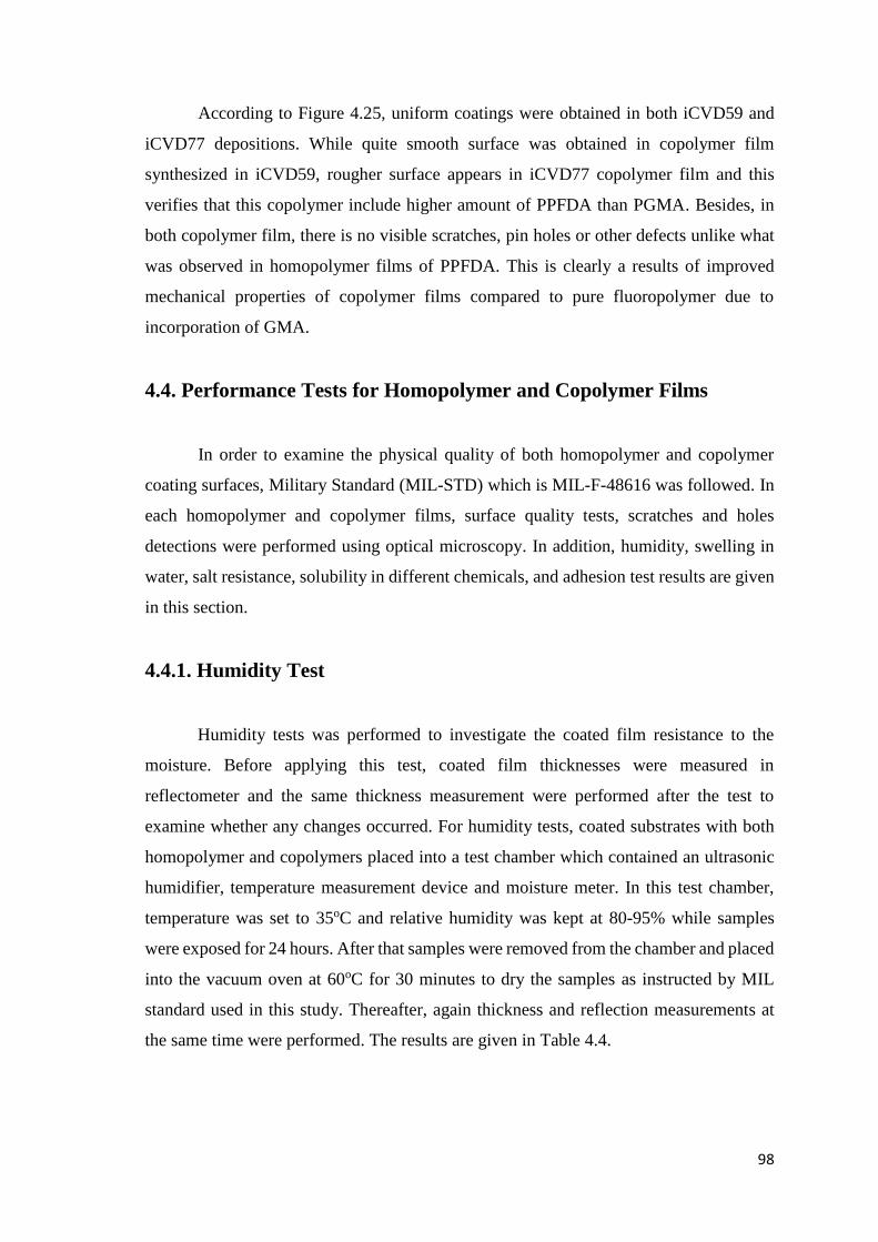
98
According to Figure 4.25, uniform coatings were obtained in both iCVD59 and
iCVD77 depositions. While quite smooth surface was obtained in copolymer film
synthesized in iCVD59, rougher surface appears in iCVD77 copolymer film and this
verifies that this copolymer include higher amount of PPFDA than PGMA. Besides, in
both copolymer film, there is no visible scratches, pin holes or other defects unlike what
was observed in homopolymer films of PPFDA. This is clearly a results of improved
mechanical properties of copolymer films compared to pure fluoropolymer due to
incorporation of GMA.
4.4. Performance Tests for Homopolymer and Copolymer Films
In order to examine the physical quality of both homopolymer and copolymer
coating surfaces, Military Standard (MIL-STD) which is MIL-F-48616 was followed. In
each homopolymer and copolymer films, surface quality tests, scratches and holes
detections were performed using optical microscopy. In addition, humidity, swelling in
water, salt resistance, solubility in different chemicals, and adhesion test results are given
in this section.
4.4.1. Humidity Test
Humidity tests was performed to investigate the coated film resistance to the
moisture. Before applying this test, coated film thicknesses were measured in
reflectometer and the same thickness measurement were performed after the test to
examine whether any changes occurred. For humidity tests, coated substrates with both
homopolymer and copolymers placed into a test chamber which contained an ultrasonic
humidifier, temperature measurement device and moisture meter. In this test chamber,
temperature was set to 35oC and relative humidity was kept at 80-95% while samples
were exposed for 24 hours. After that samples were removed from the chamber and placed
into the vacuum oven at 60oC for 30 minutes to dry the samples as instructed by MIL
standard used in this study. Thereafter, again thickness and reflection measurements at
the same time were performed. The results are given in Table 4.4.
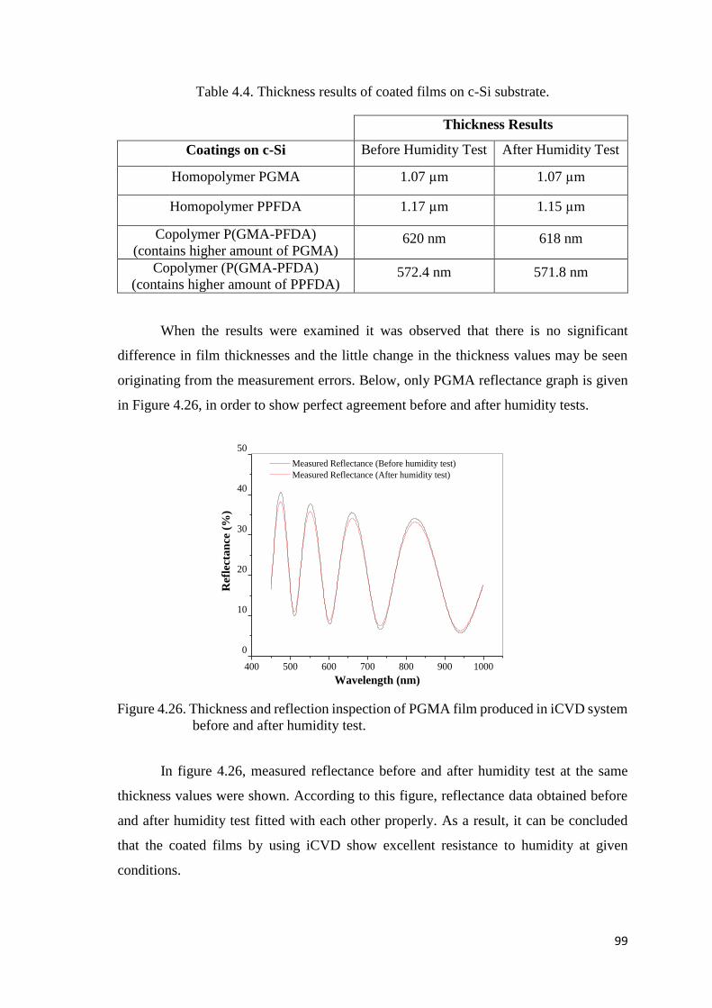
99
Table 4.4. Thickness results of coated films on c-Si substrate.
Thickness Results
Coatings on c-Si Before Humidity Test After Humidity Test
Homopolymer PGMA 1.07 µm 1.07 µm
Homopolymer PPFDA 1.17 µm 1.15 µm
Copolymer P(GMA-PFDA)
(contains higher amount of PGMA) 620 nm 618 nm
Copolymer (P(GMA-PFDA)
(contains higher amount of PPFDA) 572.4 nm 571.8 nm
When the results were examined it was observed that there is no significant
difference in film thicknesses and the little change in the thickness values may be seen
originating from the measurement errors. Below, only PGMA reflectance graph is given
in Figure 4.26, in order to show perfect agreement before and after humidity tests.
400 500 600 700 800 900 1000
0
10
20
30
40
50
Refl
ecta
nce (
%)
Wavelength (nm)
Measured Reflectance (Before humidity test)
Measured Reflectance (After humidity test)
Figure 4.26. Thickness and reflection inspection of PGMA film produced in iCVD system
before and after humidity test.
In figure 4.26, measured reflectance before and after humidity test at the same
thickness values were shown. According to this figure, reflectance data obtained before
and after humidity test fitted with each other properly. As a result, it can be concluded
that the coated films by using iCVD show excellent resistance to humidity at given
conditions.
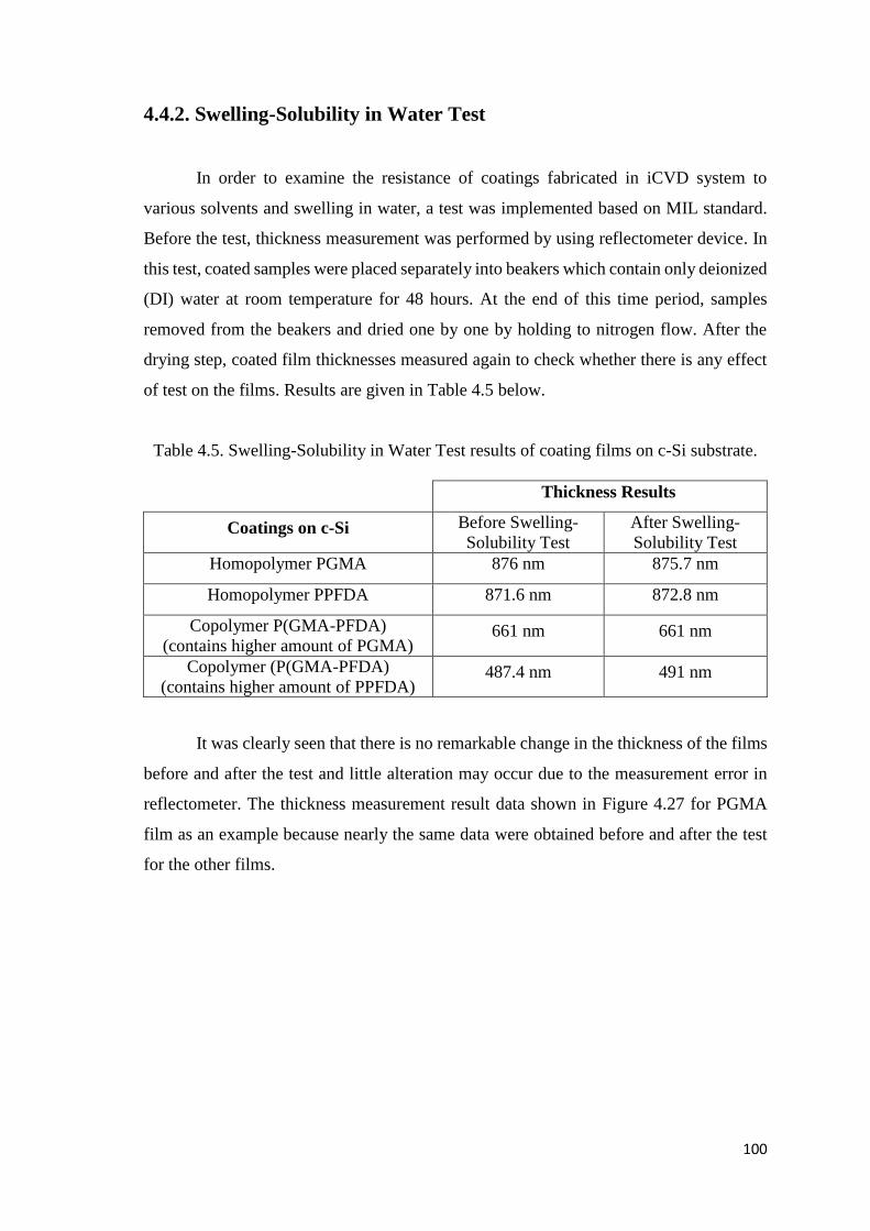
100
4.4.2. Swelling-Solubility in Water Test
In order to examine the resistance of coatings fabricated in iCVD system to
various solvents and swelling in water, a test was implemented based on MIL standard.
Before the test, thickness measurement was performed by using reflectometer device. In
this test, coated samples were placed separately into beakers which contain only deionized
(DI) water at room temperature for 48 hours. At the end of this time period, samples
removed from the beakers and dried one by one by holding to nitrogen flow. After the
drying step, coated film thicknesses measured again to check whether there is any effect
of test on the films. Results are given in Table 4.5 below.
Table 4.5. Swelling-Solubility in Water Test results of coating films on c-Si substrate.
Thickness Results
Coatings on c-Si Before Swelling-
Solubility Test
After Swelling-
Solubility Test
Homopolymer PGMA 876 nm 875.7 nm
Homopolymer PPFDA 871.6 nm 872.8 nm
Copolymer P(GMA-PFDA)
(contains higher amount of PGMA) 661 nm 661 nm
Copolymer (P(GMA-PFDA)
(contains higher amount of PPFDA) 487.4 nm 491 nm
It was clearly seen that there is no remarkable change in the thickness of the films
before and after the test and little alteration may occur due to the measurement error in
reflectometer. The thickness measurement result data shown in Figure 4.27 for PGMA
film as an example because nearly the same data were obtained before and after the test
for the other films.
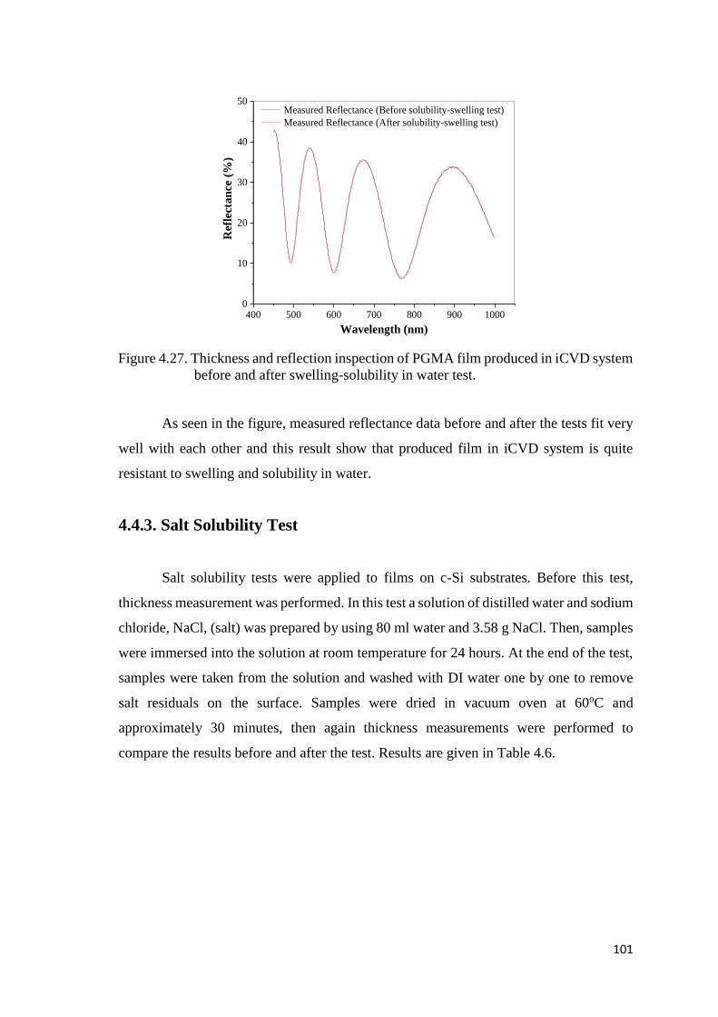
101
400 500 600 700 800 900 10000
10
20
30
40
50
Refl
ecta
nce (
%)
Wavelength (nm)
Measured Reflectance (Before solubility-swelling test)
Measured Reflectance (After solubility-swelling test)
Figure 4.27. Thickness and reflection inspection of PGMA film produced in iCVD system
before and after swelling-solubility in water test.
As seen in the figure, measured reflectance data before and after the tests fit very
well with each other and this result show that produced film in iCVD system is quite
resistant to swelling and solubility in water.
4.4.3. Salt Solubility Test
Salt solubility tests were applied to films on c-Si substrates. Before this test,
thickness measurement was performed. In this test a solution of distilled water and sodium
chloride, NaCl, (salt) was prepared by using 80 ml water and 3.58 g NaCl. Then, samples
were immersed into the solution at room temperature for 24 hours. At the end of the test,
samples were taken from the solution and washed with DI water one by one to remove
salt residuals on the surface. Samples were dried in vacuum oven at 60oC and
approximately 30 minutes, then again thickness measurements were performed to
compare the results before and after the test. Results are given in Table 4.6.
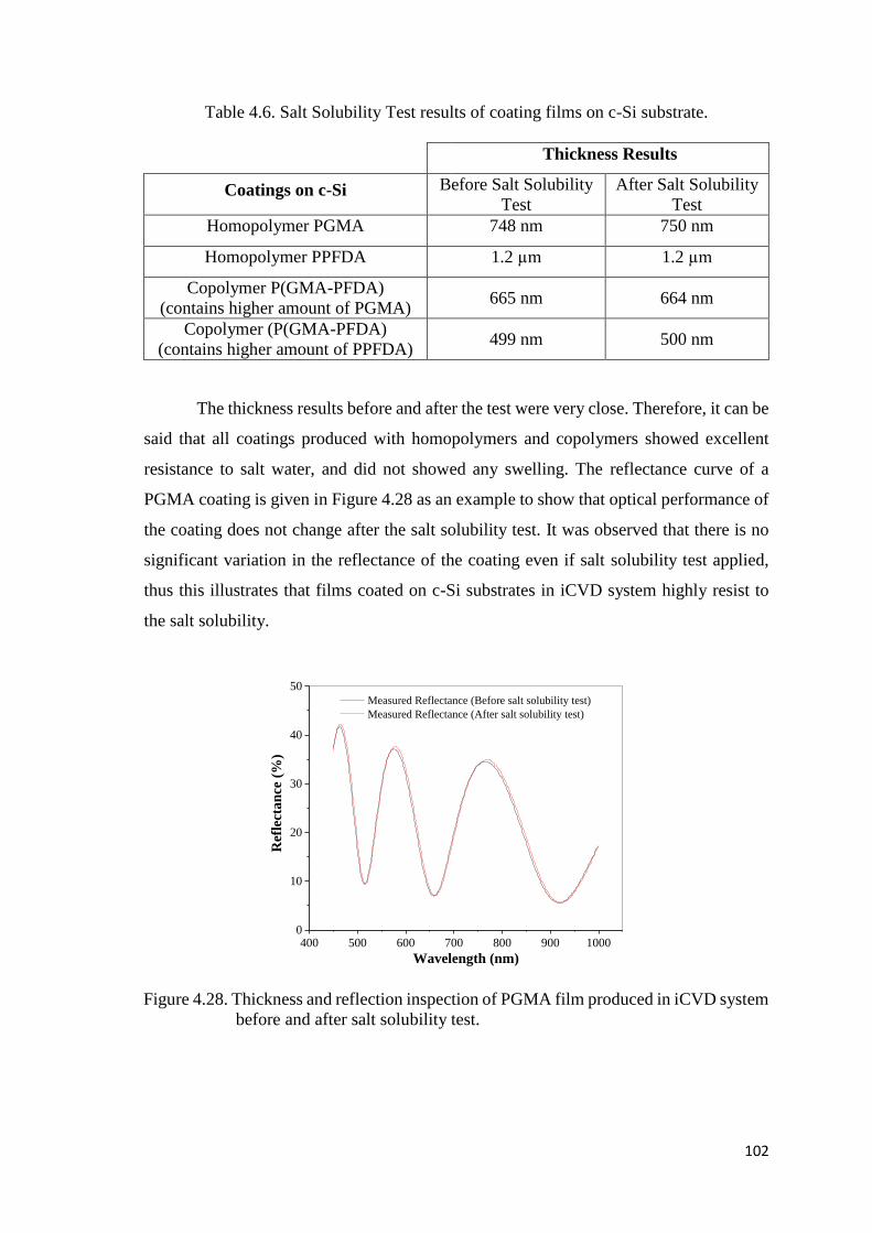
102
Table 4.6. Salt Solubility Test results of coating films on c-Si substrate.
Thickness Results
Coatings on c-Si Before Salt Solubility
Test
After Salt Solubility
Test
Homopolymer PGMA 748 nm 750 nm
Homopolymer PPFDA 1.2 µm 1.2 µm
Copolymer P(GMA-PFDA)
(contains higher amount of PGMA) 665 nm 664 nm
Copolymer (P(GMA-PFDA)
(contains higher amount of PPFDA) 499 nm 500 nm
The thickness results before and after the test were very close. Therefore, it can be
said that all coatings produced with homopolymers and copolymers showed excellent
resistance to salt water, and did not showed any swelling. The reflectance curve of a
PGMA coating is given in Figure 4.28 as an example to show that optical performance of
the coating does not change after the salt solubility test. It was observed that there is no
significant variation in the reflectance of the coating even if salt solubility test applied,
thus this illustrates that films coated on c-Si substrates in iCVD system highly resist to
the salt solubility.
400 500 600 700 800 900 10000
10
20
30
40
50
Ref
lect
an
ce (
%)
Wavelength (nm)
Measured Reflectance (Before salt solubility test)
Measured Reflectance (After salt solubility test)
Figure 4.28. Thickness and reflection inspection of PGMA film produced in iCVD system
before and after salt solubility test.
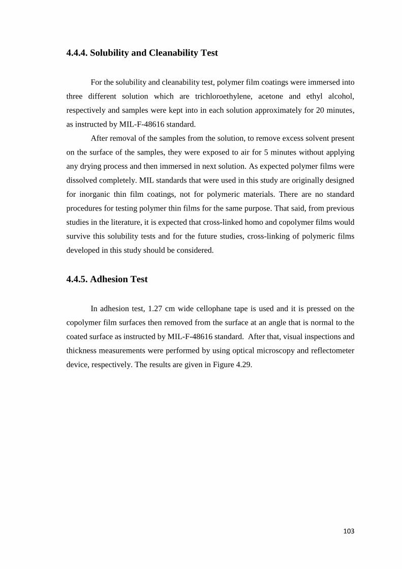
103
4.4.4. Solubility and Cleanability Test
For the solubility and cleanability test, polymer film coatings were immersed into
three different solution which are trichloroethylene, acetone and ethyl alcohol,
respectively and samples were kept into in each solution approximately for 20 minutes,
as instructed by MIL-F-48616 standard.
After removal of the samples from the solution, to remove excess solvent present
on the surface of the samples, they were exposed to air for 5 minutes without applying
any drying process and then immersed in next solution. As expected polymer films were
dissolved completely. MIL standards that were used in this study are originally designed
for inorganic thin film coatings, not for polymeric materials. There are no standard
procedures for testing polymer thin films for the same purpose. That said, from previous
studies in the literature, it is expected that cross-linked homo and copolymer films would
survive this solubility tests and for the future studies, cross-linking of polymeric films
developed in this study should be considered.
4.4.5. Adhesion Test
In adhesion test, 1.27 cm wide cellophane tape is used and it is pressed on the
copolymer film surfaces then removed from the surface at an angle that is normal to the
coated surface as instructed by MIL-F-48616 standard. After that, visual inspections and
thickness measurements were performed by using optical microscopy and reflectometer
device, respectively. The results are given in Figure 4.29.
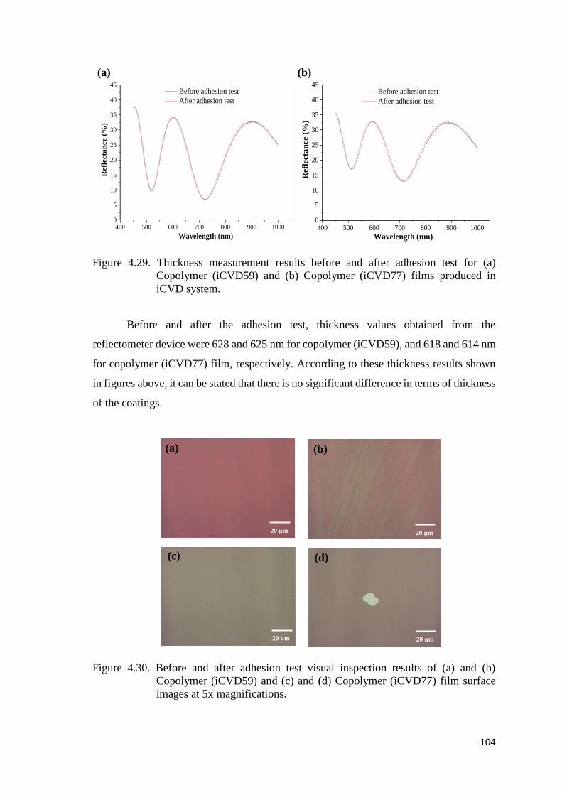
104
(a)
400 500 600 700 800 900 10000
5
10
15
20
25
30
35
40
45
Refl
ecta
nce (
%)
Wavelength (nm)
Before adhesion test
After adhesion test
(b)
400 500 600 700 800 900 10000
5
10
15
20
25
30
35
40
45
Refl
ecta
nce (
%)
Wavelength (nm)
Before adhesion test
After adhesion test
Figure 4.29. Thickness measurement results before and after adhesion test for (a)
Copolymer (iCVD59) and (b) Copolymer (iCVD77) films produced in
iCVD system.
Before and after the adhesion test, thickness values obtained from the
reflectometer device were 628 and 625 nm for copolymer (iCVD59), and 618 and 614 nm
for copolymer (iCVD77) film, respectively. According to these thickness results shown
in figures above, it can be stated that there is no significant difference in terms of thickness
of the coatings.
Figure 4.30. Before and after adhesion test visual inspection results of (a) and (b)
Copolymer (iCVD59) and (c) and (d) Copolymer (iCVD77) film surface
images at 5x magnifications.
20 µm
(a) (b)
20 µm
20 µm 20 µm
(c) (d)
105
When optical microscopy analysis was performed, it was observed that after the
adhesion test, there is no significant change on the coating surface of the copolymer
(iCVD59) film thus concluded that copolymer (iCVD59) survived adhesion test
successfully. However, in copolymer (iCVD77) coating, a small piece of the film stuck
to the cellophane tape and was removed from the surface. This was expected because the
mechanical properties of this copolymer film was expected to be poorer than the iCVD59
film due to higher amount of PFDA in its composition. However, compared to total area
of the film that the area of piece of film that was removed from the substrate is still within
acceptable range. So by carefully controlling the copolymer film composition, mechanical
strength and adhesion of the film to the substrate surface can be improved. As a result,
even if iCVD77 copolymer film not show very high resistance to the adhesion test as seen
in the copolymer iCVD59, it can still be said that this copolymer film also was durable to
this test when both thickness and visual inspection results considered.
106
CHAPTER 5
CONCLUSIONS
In this study, fabrication of protective, self-cleaning and super hydrophobic
polymeric film coatings for optical surfaces of the electro-optical systems were performed
on both c-Si and glass substrates. In order to achieve desired mechanical, chemical and
surface properties as well as to meet minimum optical performance criteria optimum
operating conditions in iCVD system were determined for a variety of homo- and
copolymer film coatings.
In order to obtain coatings with unique properties specified by the application
GMA and PFDA were used as monomers; GMA for excellent mechanical and adhesion
properties and PFDA for providing super hydrophobicity. Another reason for using these
monomers in this study is that their refractive indices are close to glass substrate and this
is very significant to preserve optical performance of especially glass type optic surfaces
used in the electro-optical systems. Before depositions, modeling and simulation of the
coatings to determine optimum film thickness was completed and simulation results
showed that optical performance of the substrate surfaces preserved successfully even if
the film thickness varied from 50 nm to 1 µm.
Homopolymers of PGMA and PPFDA thins films with varying thicknesses were
deposited on c-Si and glass substrates via iCVD process. PGMA homopolymer films
showed excellent mechanical and optical properties, however, hydrophobicity of the
surface was not sufficient to be used as protective optical coatings in EO systems. On the
other hand, PPFDA homopolymer films showed excellent surface hydrophobicity but also
showed very poor mechanical properties, and were very prone to scratches and other
surface damage by mechanical handling.
In order to take advantage of good mechanical properties of PGMA and
hydrophobicity of PPFDA, P(GMA-PFDA) copolymers were fabricated via iCVD
process. It was found that optical and mechanical properties of copolymers can be finely
tuned by controlling the flow rates of monomers during iCVD deposition process.
To investigate the suitability of using these thin films as protective optical coating
in EO systems, additional tests based on MIL-F-48616 standard were performed for
homopolymer and copolymer films.

107
It was concluded that both homopolymer and copolymer films deposited in iCVD
system show high resistance to humidity, salt solubility, swelling and solubility in water.
Also, copolymer film which has higher amount of GMA is quite resistance to adhesion
test. Therefore, it can be concluded that especially copolymer films produced in this study
are quite suitable for coating on optical surfaces of the electro-optical surfaces.
108
REFERENCES
Alf, M. E., T. A. Hatton and K. K. Gleason (2011). "Initiated chemical vapor deposition
of responsive polymeric surfaces." Thin Solid Films 519(14): 4412-4414.
Allcock, H. R., F. W. Lampe and J. E. Mark (2003). Contemporary Polymer Chemistry,
Prentice Hall.
Andrews, D. L. (2009). Encyclopedia of Applied Spectroscopy, Wiley.
Bakker, R., V. Verlaan, C. H. M. van der Werf, J. K. Rath, K. K. Gleason and R. E. I.
Schropp (2007). "Initiated chemical vapour deposition (iCVD) of thermally stable
poly-glycidyl methacrylate." Surface and Coatings Technology 201(22–23):
9422-9425.
Bass, M., C. DeCusatis, J. Enoch, V. Lakshminarayanan, G. Li, C. MacDonald, V.
Mahajan and E. Van Stryland (2009). Handbook of Optics, Third Edition Volume
IV: Optical Properties of Materials, Nonlinear Optics, Quantum Optics (set),
McGraw-Hill Education.
Bose, R. K., K. Lau, U. Drexel and E. College of (2011). Initiated chemical vapor
deposition of polymer thin films and coatings for biological applications, Drexel
University.
Callister, W. D. (2007). Materials Science And Engineering: An Introduction, John Wiley
& Sons.
Campana, S. (1993). The Infrared & Electro-Optical Systems Handbook. Passive
Ellectro-Optical Systems, Infrared information and analysis center ann arbor mi.
Chan, K. and K. K. Gleason (2006). "A Mechanistic Study of Initiated Chemical Vapor
Deposition of Polymers: Analyses of Deposition Rate and Molecular Weight."
Macromolecules 39(11): 3890-3894.
Chan, K., L. E. Kostun, W. E. Tenhaeff and K. K. Gleason (2006). "Initiated chemical
vapor deposition of polyvinylpyrrolidone-based thin films." Polymer 47(20):
6941-6947.
Coclite, A. M. (2013). "Smart surfaces by initiated chemical vapor deposition." Surface
Innovations 1(1): 6-14.
Coclite, A. M., Y. Shi and K. K. Gleason (2013). "Super-Hydrophobic and Oloephobic
Crystalline Coatings by Initiated Chemical Vapor Deposition." Physics Procedia
46: 56-61.
Dorval Dion, C. A. and J. R. Tavares (2013). "Photo-initiated chemical vapor deposition
as a scalable particle functionalization technology (a practical review)." Powder
Technology 239: 484-491.
109
Driggers, R. G., P. Cox and T. Edwards (1999). Introduction to Infrared and Electro-
optical Systems, Artech House.
Dudzik, M. (1993). The Infrared & Electro-Optical Systems Handbook. Electro-Optical
Systems Design, Analysis, and Testing, Infrared information and analysis center
ann arbor mi.
Fox, C. (1996). The Infrared and Electro-optical Systems Handbook: Actives electro-
optical systems, Environmental research institute of Michigan.
Gleason, K. K. (2015). CVD Polymers: Fabrication of Organic Surfaces and Devices,
Wiley.
Gupta, M. and K. K. Gleason (2006). "Initiated Chemical Vapor Deposition of
Poly(1H,1H,2H,2H-perfluorodecyl Acrylate) Thin Films." Langmuir 22(24):
10047–10052.
Gupta, M. and K. K. Gleason (2006). "Large-scale initiated chemical vapor deposition of
poly(glycidyl methacrylate) thin films." Thin Solid Films 515(4): 1579-1584.
Gupta, M. and K. K. Gleason (2009). "Surface modification of high aspect ratio structures
with fluoropolymer coatings using chemical vapor deposition." Thin Solid Films
517(12): 3547-3550.
Gupta, M., V. Kapur, N. M. Pinkerton and K. K. Gleason (2008). "Initiated Chemical
Vapor Deposition (iCVD) of Conformal Polymeric Nanocoatings for the Surface
Modification of High-Aspect-Ratio Pores." Chemistry of Materials 20 (4): 1646–
1651.
Johnson, R. W., A. Hultqvist and S. F. Bent (2014). "A brief review of atomic layer
deposition: from fundamentals to applications." Materials Today 17(5): 236-246.
Jones, A. C. and M. L. Hitchman (2009). Chemical Vapour Deposition: Precursors,
Processes and Applications, Royal Society of Chemistry.
Lau, K. K. S. and K. K. Gleason (2006). "Initiated chemical vapor deposition (iCVD) of
poly( alkyl acrylates): An experimental study." Macromolecules 39(10): 3688-
3694.
Lau, K. K. S. and K. K. Gleason (2006). "Initiated chemical vapor deposition (iCVD) of
poly(alkyl acrylates): A kinetic model." Macromolecules 39(10): 3695-3703.
Lau, K. K. S. and K. K. Gleason (2007). "Particle functionalization and encapsulation by
initiated chemical vapor deposition (iCVD)." Surface and Coatings Technology
201(22–23): 9189-9194.
Lau, K. K. S. and K. K. Gleason (2008). "Applying HWCVD to particle coatings and
modeling the deposition mechanism." Thin Solid Films 516(5): 674-677.
110
Lau, K. K. S. and K. K. Gleason (2008). "Initiated chemical vapor deposition (iCVD) of
copolymer thin films." Thin Solid Films 516(5): 678-680.
Luis, Y. J. and K. K. Gleason (2013). "Enhanced Cross-Linked Density by Annealing on
Fluorinated Polymers Synthesized via Initiated Chemical Vapor Deposition To
Prevent Surface Reconstruction." Macromolecules 46(16): 6548–6554.
Lvovsky, A. I. (2013). Fresnel Equations. In Encyclopedia of Optical Engineering, Taylor
and Francis: New York: 1-6.
MacLeod, H. A. (2001). Thin-Film Optical Filters, Third Edition, Taylor & Francis.
Mao, Y. and K. K. Gleason (2004). "Hot Filament Chemical Vapor Deposition of
Poly(glycidyl methacrylate) Thin Films Using tert-Butyl Peroxide as an Initiator."
Langmuir 20(6): 2484-2488.
Mao, Y. and K. K. Gleason (2006). "Vapor-Deposited Fluorinated Glycidyl Copolymer
Thin Films with Low Surface Energy and Improved Mechanical Properties."
Macromolecules 39(11): 3895-3900.
Martin, T. P., S. E. Kooi, S. H. Chang, K. L. Sedransk and K. K. Gleason (2007). "Initiated
chemical vapor deposition of antimicrobial polymer coatings." Biomaterials
28(6): 909-915.
Martin, T. P., K. K. S. Lau, K. Chan, Y. Mao, M. Gupta, A. S. O'Shaughnessy and K. K.
Gleason (2007). "Initiated chemical vapor deposition (iCVD) of polymeric
nanocoatings." Surface & Coatings Technology 201(22-23): 9400-9405.
Mittal, V. (2013). Encapsulation Nanotechnologies, Wiley.
Mohammed Safiullah, S., K. Abdul Wasi and K. Anver Basha (2014). "Preparation of
poly(Glycidyl methacrylate)–copper nanocomposite by in-situ suspension
polymerization – A novel synthetic method." Materials Letters 133: 60-63.
Nalwa, H. S. and S. Miyata (1996). Nonlinear Optics of Organic Molecules and Polymers,
Taylor & Francis.
Park, S. W., D. Lee, H. R. Lee, H.-J. Moon, B. R. Lee, W.-K. Ko, S.-J. Song, S. J. Lee,
K. Shin, W. Jang, J.-K. Yi, S. G. Im and I. K. Kwon (2015). "Generation of
functionalized polymer nanolayer on implant surface via initiated chemical vapor
deposition (iCVD)." Journal of Colloid and Interface Science 439: 34-41.
Parker, T. C., D. Baechle and J. D. Demaree (2011). "Polymeric barrier coatings via
initiated chemical vapor deposition." Surface and Coatings Technology 206(7):
1680-1683.
Piegari, A. and F. Flory (2013). Optical Thin Films and Coatings: From Materials to
Applications, Elsevier Science.
111
Pierson, H. O. (1999). Handbook of Chemical Vapor Deposition, 2nd Edition: Principles,
Technology and Applications, Elsevier Science.
Riche, C. T., C. Zhang, M. Gupta and N. Malmstadt (2014). "Fluoropolymer surface
coatings to control droplets in microfluidic devices." The Royal Society of
Chemistry 14: 1834–1841.
Schaub, M. P. (2009). The Design of Plastic Optical Systems, Society of Photo Optical.
Stenzel, O. (2006). The Physics of Thin Film Optical Spectra: An Introduction, Springer
Berlin Heidelberg.
Stuart, B. H. (2004). Infrared Spectroscopy: Fundamentals and Applications, Wiley.
Träger, F. (2012). Springer Handbook of Lasers and Optics, Springer.
Trujillo, N. J., Q. G. Wu and K. K. Gleason (2010). "Ultralow Dielectric Constant
Tetravinyltetramethylcyclotetrasiloxane Films Deposited by Initiated Chemical
Vapor Deposition (iCVD)." Advanced Functional Materials 20(4): 607-616.
Turner, T. and R. Kirschner. "Thin-Film Coatings." Retrieved (2015 September, 11),
from http://www.photonics.com/EDU/Handbook.aspx?AID=42399.
Wakaki, M. (2012). Optical Materials and Applications, Taylor & Francis.
Web-1. (2012). "Refraction of Light." Retrieved ( 2015 September, 8 ), from
http://sciencelearn.org.nz/Contexts/Light-and-Sight/Science-Ideas-and-
Concepts/Refraction-of-light.
Web-2. "Light Properties: Absorption, Reflection and Transmission." Retrieved ( 2015
September, 11), from
http://www.easycoursesportal.com/basicphotographycourseiii/coursec/Less-
8.htm.
Web-3. "Crystal Systems." Retrieved (2015 September, 13), from
https://wwwf.imperial.ac.uk/earthscienceandengineering/rocklibrary/viewglossre
cord.php?Term=crystal%20system.
Web-4. "Tracking Solar Flares." Retrieved (2015 September, 18), from http://solar-
center.stanford.edu/SID/activities/ionosphere.html.
Web-5. "Anti-Reflection Coatings." Retrieved (2015 September, 18), from
http://hyperphysics.phy-astr.gsu.edu/hbase/phyopt/antiref.html.
Web-6. "Optical Coatings." Retrieved (2015 September, 19), from
http://cvilaseroptics.com/Frontend/PDFs/optical_coatings.pdf.
Web-7. "Hot&Cold Mirrors." Retrieved (2015 September, 28), from
http://www.uqgoptics.com/product_custom_filters_mirrors.aspx.
112
Web-8. "Optical Filters: Hot and Cold Mirrors." Retrieved (2015 September, 28), from
http://www.optical-filters.com/Filters.aspx.
Web-9. "Transmission spectra of substrate materials." Retrieved (2016 January, 2), from
http://www.thorlabs.de/NewGroupPage9.cfm?ObjectGroup_ID=3982.
Web-10. "Material Transmission Data." Retrieved (2016 January, 2), from
http://rmico.com/support/tech-notes/material-data#mgf2.
Weber, M. J. (2002). Handbook of Optical Materials, Taylor & Francis.
Wypych, G. (2011). Handbook of Polymers, ChemTec Pub.
Yoo, Y., J. B. You, W. Choi and S. G. Im (2013). "A stacked polymer film for robust
superhydrophobic fabrics." Polymer Chemistry 4(5): 1664-1671.