Embed Size (px)
Citation preview

Developments in high bandwidth power amplifier technology forcompact cost effective calibrator applications.
Paul C. A. Roberts - Applied Technology Manager,Fluke Precision Measurement Limited, UK.
Abstract:
The workload of a modern calibration laboratory has placed ever greater demands on theCalibration Source, both in terms of functionality and the combination of voltage, current andfrequency required to calibrate today's diverse range of instruments.
This need for high voltage and high current at high frequency into demanding loads such asclamp meters and current coils, combined with a desire to produce ever more economic andcompact calibrators, has resulted in a number of significant developments in the transition fromthe vacuum tube designs common in the past to today's solid state designs employing the latestsemiconductor and transformer technologies.
This paper explores the development of technologies enabling the design of high bandwidthpower amplifiers compact enough to be integrated within the calibrator in a single enclosure,eliminating the need for a separate Boost Amplifier, and their impact on calibration applications.
Introduction:
During the 1970s a number of alternating voltage calibrators were successfully developed anddeployed, but where a high voltage output was required a separate power or boost amplifierwas always involved. These designs were based on vacuum tubes, often utilizing tubes designedas UHF radio transmitters because of their availability in suitable power ratings and theirphysical suitability for mechanical mounting. Reliability was poor and many manufacturersproducts earned a well deserved reputation for fragility - and with one exception thosemanufacturers either collapsed or chose to leave the calibration business. The most successfulAC voltage calibrator/amplifier partnership continued into the 1980s and was the competitivetarget for a new generation of AC voltage calibrator released in 1984 - the Datron 4200.
This new design employed fully solid state technology with an integrated power amplifiercapable of delivering 1000V at frequencies up to 30kHz extending to 100kHz at 750V. Thesize of this unit was identical to its closest competitor which could only provide 200V - theadditional vacuum tube boost amplifier required to obtain 1000V capability occupied almosttwice the volume of its partner. Analysis of workloads revealed that high voltage capability at
high frequency was an essential requirement for complete calibration of the precision DMMsappearing on the market at that time - one in particular which required 700V at 100kHz. Andthis even in the days before ISO9000 was driving the need for complete calibrations!. However,output current requirements were within the capabilities of semiconductors - vacuum tubedesigns were overkill for the actual workload in this respect.
The technology which enabled such a compact power amplifier design was the powerMOSFET transistor. The following sections of this paper discuss the design requirements andtheir implementations in more detail. Initially, for the voltage amplifier used in the Datron 4700series multifunction calibrators launched in 1986 (developed from the original AC voltagecalibrator design) and employed with further development in the Wavetek 4800 seriesintroduced in 1991. The paper continues by exploring the current source amplifier used withinthe recently introduced 9100 universal calibrator capable of delivering 20Amps at 10kHz froman enclosure smaller than the original AC voltage only design whilst coping with the demandingload that an external current coil can present.
Design and Development of the Solid State Voltage Power amplifier:
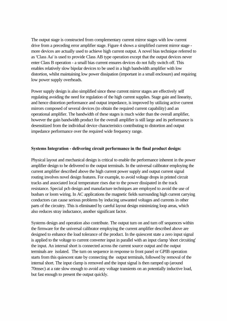
The design requirements for the multifunction calibrator (4800 series) were to provide a poweramplifier capable of sourcing the output voltages for the DC and AC 100V and 1000V ranges.This required a high bandwidth design capable of providing up to 200V RMS at 100kHzreducing to 20V at 1MHz directly from the same amplifier that could also operate as a lownoise DC source for the DCV ranges and drive a step up transformer to provide the 1000Vrange at frequencies up to 30kHz, extending at reducing voltage to 100kHz at 750V. (In the1000V DC range the power amp/transformer provide a signal which is rectified and filtered togenerate the DC output). Additional constraints were weight, size and load into which theselevels must be driven. The most stringent requirement is the 1000V capability requiring deliveryinternally of 180V RMS at 1A into the 6:1 step up transformer primary to satisfy the required,mainly capacitive, load current. (At high frequency the dominant load is the capacitance ofcables connecting the calibrator to its workload and internal signal path capacitance.
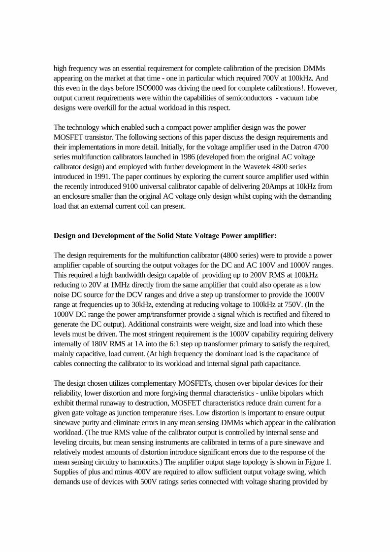
The design chosen utilizes complementary MOSFETs, chosen over bipolar devices for theirreliability, lower distortion and more forgiving thermal characteristics - unlike bipolars whichexhibit thermal runaway to destruction, MOSFET characteristics reduce drain current for agiven gate voltage as junction temperature rises. Low distortion is important to ensure outputsinewave purity and eliminate errors in any mean sensing DMMs which appear in the calibrationworkload. (The true RMS value of the calibrator output is controlled by internal sense andleveling circuits, but mean sensing instruments are calibrated in terms of a pure sinewave andrelatively modest amounts of distortion introduce significant errors due to the response of themean sensing circuitry to harmonics.) The amplifier output stage topology is shown in Figure 1.Supplies of plus and minus 400V are required to allow sufficient output voltage swing, whichdemands use of devices with 500V ratings series connected with voltage sharing provided by

the resistors marked Rx. Devices are paralleled to increase the current capability. Those familiarwith high performance audio design will recognize elements of this topology. The voltagecapability of P-channel MOSFETs is much more restricted than N-channel devices due tosemiconductor physics - the lower charge carrier mobilities of P-type material impacts devicegeometry and has limited currently available devices to 500V. The N channel devices employedare actually rated at 800V and are chosen not for voltage rating but to match the capacitance ofthe P-channel devices and provide a truly complementary design. The high input capacitance ofMOSFETs, typically 1nanofarad per device, poses a difficult load for the driver stages andimposes a limit on the achievable slew rate which is more restrictive than attaining the bandwidthtarget - if the amplifier or any of its parts slew rate limit distortion will be introduced into theoutput waveform which the local negative feedback around the amplifier will not be able toreduce - in effect the amplifier fails to keep up with itself. Other novel features include adistortion canceling circuit which cancels distortion introduced in a pre-driver cascode stageresulting from the drain-gate capacitance of another MOSFET which varies non linearly withvoltage. The achieved Volt-Hertz profile is presented in Figure 2.
Design and Development of the Current Power amplifier:
Design objectives for the 9100 universal calibrator were to produce a precision high currentsource capable of delivering up to 20A at DC with compliance voltages up to 4V, and up to20A AC from 10Hz to 10kHz (30kHz at lower currents) into a 700µH load with compliancevoltages up to 2.5V RMS. (Inductive load capability is limited at higher frequencies by thecompliance voltage developed across the load). High output impedance is critical in producing aconstant current source to avoid compliance errors. The workload requiring this capability arethe common current clamp meters or clamp accessories which typically measure currents up to1000A. To achieve these high currents a pair of ten and fifty turn current coil accessories weredesigned to accompany the calibrator. Magnetic shielding within the coil minimizes the influenceof stray fields and allows a physically small low inductance design. However, the coil inductanceis significantly modified (increased) by applying the clamp, with the hall effect clamps presentingthe most difficult loads. Producing a compact calibrator design was the other objective ofenabling a small and easily transported single enclosure unit to supply the wide functionalityneeded to address the diverse workload now common in calibration labs - from handheldDMMs through analog meters and frequency counters to oscilloscopes.
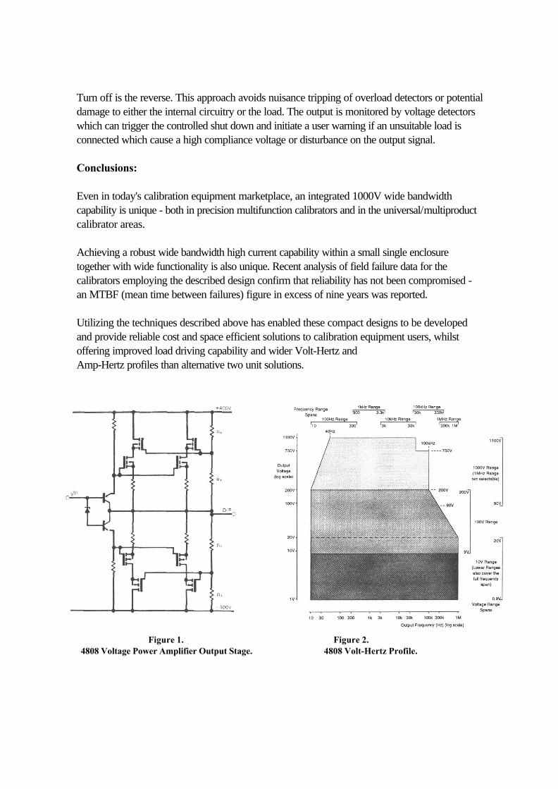
The topology chosen was a ground sensed voltage to current converter employing bipolartransistors in the power output stages, shown in block form in Figure 3. In this case bipolartransistors were chosen over MOSFET devices due to their better cost/performance ratio in thisapplication. Bipolars have a lower thermal resistance than MOSFETs for a given currentrequiring fewer devices for a given power dissipation capability, and they have lowercapacitance - bipolars do not suffer the high gate input capacitance of MOSFETs and havelower output capacitance which simplify driver circuits and improve output impedance of thecurrent source.
The output stage is constructed from complementary current mirror stages with low currentdrive from a preceding error amplifier stage. Figure 4 shows a simplified current mirror stage -more devices are actually used to achieve high current output. A novel bias technique referred toas 'Class Aa' is used to provide Class AB type operation except that the output devices neverenter Class B operation - a small bias current ensures devices do not fully switch off. Thisenables relatively slow bipolar devices to be used in a high bandwidth amplifier with lowdistortion, whilst maintaining low power dissipation (important in a small enclosure) and requiringlow power supply overheads.
Power supply design is also simplified since these current mirror stages are effectively selfregulating avoiding the need for regulation of the high current supplies. Stage gain and linearity,and hence distortion performance and output impedance, is improved by utilizing active currentmirrors composed of several devices (to obtain the required current capability) and anoperational amplifier. The bandwidth of these stages is much wider than the overall amplifier,however the gain bandwidth product for the overall amplifier is still large and its performance isdesensitized from the individual device characteristics contributing to distortion and outputimpedance performance over the required wide frequency range.
Systems Integration - delivering circuit performance in the final product design:
Physical layout and mechanical design is critical to enable the performance inherent in the poweramplifier design to be delivered to the output terminals. In the universal calibrator employing thecurrent amplifier described above the high current power supply and output current signalrouting involves novel design features. For example, to avoid voltage drops in printed circuittracks and associated local temperature rises due to the power dissipated in the trackresistance. Special pcb design and manufacture techniques are employed to avoid the use ofbusbars or loom wiring. In AC applications the magnetic fields surrounding high current carryingconductors can cause serious problems by inducing unwanted voltages and currents in otherparts of the circuitry. This is eliminated by careful layout design minimizing loop areas, whichalso reduces stray inductance, another significant factor.
Systems design and operation also contribute. The output turn on and turn off sequences withinthe firmware for the universal calibrator employing the current amplifier described above aredesigned to enhance the load tolerance of the product. In the quiescent state a zero input signalis applied to the voltage to current converter input in parallel with an input clamp 'short circuiting'the input. An internal short is connected across the current source output and the outputterminals are isolated. The turn on sequence in response to front panel or GPIB operationstarts from this quiescent state by connecting the output terminals, followed by removal of theinternal short. The input clamp is removed and the input signal is then ramped up (around70msec) at a rate slow enough to avoid any voltage transients on an potentially inductive load,but fast enough to present the output quickly.
Turn off is the reverse. This approach avoids nuisance tripping of overload detectors or potentialdamage to either the internal circuitry or the load. The output is monitored by voltage detectorswhich can trigger the controlled shut down and initiate a user warning if an unsuitable load isconnected which cause a high compliance voltage or disturbance on the output signal.
Conclusions:
Even in today's calibration equipment marketplace, an integrated 1000V wide bandwidthcapability is unique - both in precision multifunction calibrators and in the universal/multiproductcalibrator areas.
Achieving a robust wide bandwidth high current capability within a small single enclosuretogether with wide functionality is also unique. Recent analysis of field failure data for thecalibrators employing the described design confirm that reliability has not been compromised -an MTBF (mean time between failures) figure in excess of nine years was reported.
Utilizing the techniques described above has enabled these compact designs to be developedand provide reliable cost and space efficient solutions to calibration equipment users, whilstoffering improved load driving capability and wider Volt-Hertz andAmp-Hertz profiles than alternative two unit solutions.
Figure 1. Figure 2. 4808 Voltage Power Amplifier Output Stage. 4808 Volt-Hertz Profile.
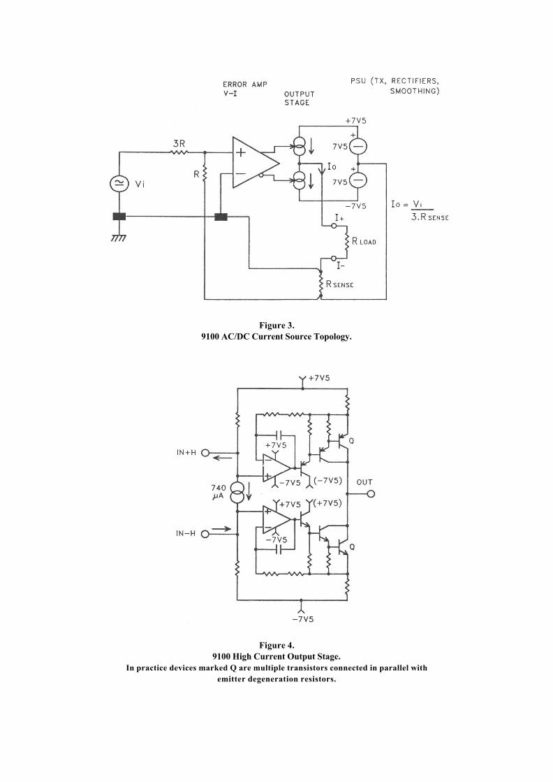
Figure 3.9100 AC/DC Current Source Topology.
Figure 4.9100 High Current Output Stage.
In practice devices marked Q are multiple transistors connected in parallel withemitter degeneration resistors.