Embed Size (px)
Citation preview
March 2017 Altera Corporation
ES-01036-3.1 Errata Sheet
© 2017 Altera Corporation. All rights reserved. ALTERA, ARRIA, CYCLONE, HARDCOPY, MAX, MEGACORE, NIOS, QUARTUS and STRATIX words and logos are trademarks of Altera Corporation and registered in the U.S. Patent and Trademark Office and in other countries. All other words and logos identified as trademarks or service marks are the property of their respective holders as described at www.altera.com/common/legal.html. Altera warrants performance of its semiconductor products to current specifications in accordance with Altera's standard warranty, but reserves the right to make changes to any products and services at any time without notice. Altera assumes no responsibility or liability arising out of the application or use of any information, product, or service described herein except as expressly agreed to in writing by Altera. Altera customers are advised to obtain the latest version of device specifications before relying on any published information and before placing orders for products or services.
101 Innovation DriveSan Jose, CA 95134www.altera.com
Subscribe
ISO 9001:2008 Registered
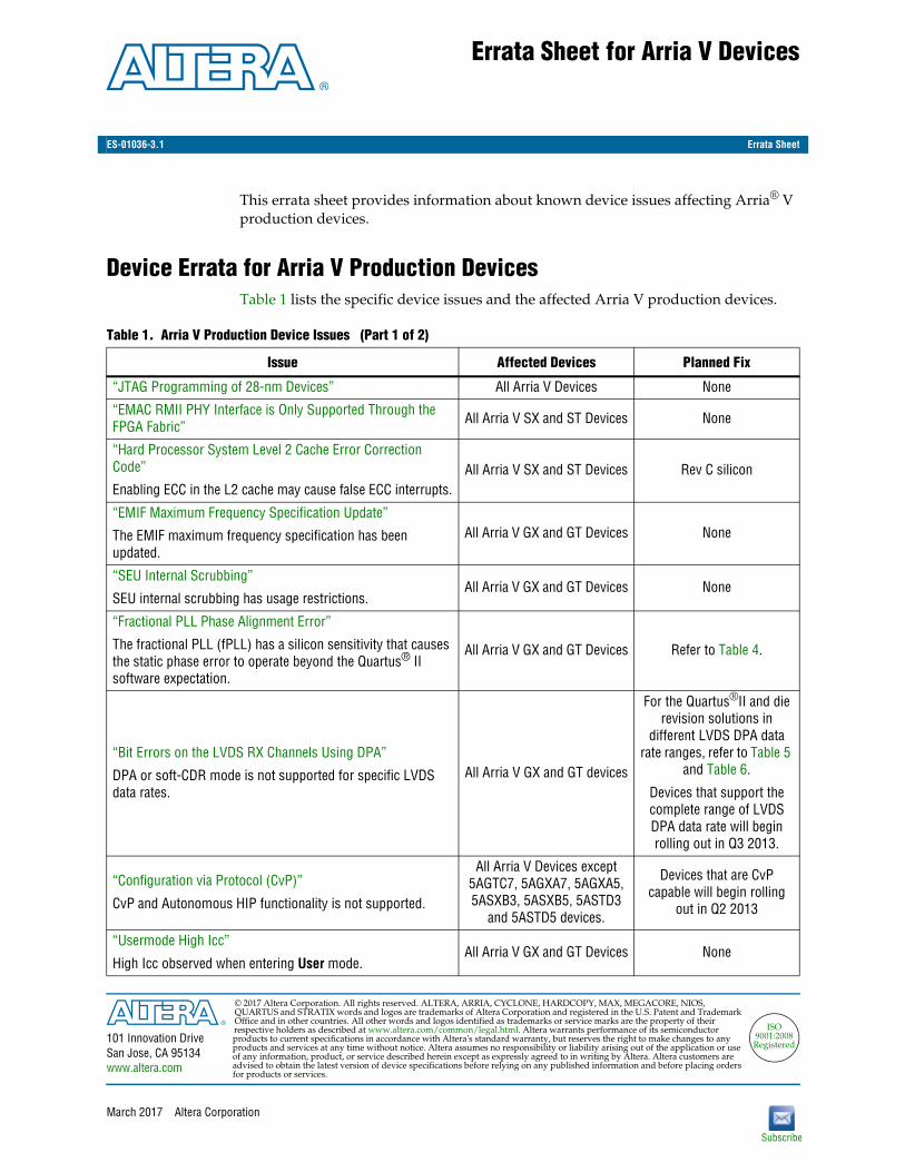
Errata Sheet for Arria V Devices
This errata sheet provides information about known device issues affecting Arria® V production devices.
Device Errata for Arria V Production DevicesTable 1 lists the specific device issues and the affected Arria V production devices.
Table 1. Arria V Production Device Issues (Part 1 of 2)
Issue Affected Devices Planned Fix
“JTAG Programming of 28-nm Devices” All Arria V Devices None
“EMAC RMII PHY Interface is Only Supported Through the FPGA Fabric” All Arria V SX and ST Devices None
“Hard Processor System Level 2 Cache Error Correction Code”
Enabling ECC in the L2 cache may cause false ECC interrupts.All Arria V SX and ST Devices Rev C silicon
“EMIF Maximum Frequency Specification Update”
The EMIF maximum frequency specification has been updated.
All Arria V GX and GT Devices None
“SEU Internal Scrubbing”
SEU internal scrubbing has usage restrictions.All Arria V GX and GT Devices None
“Fractional PLL Phase Alignment Error”
The fractional PLL (fPLL) has a silicon sensitivity that causes the static phase error to operate beyond the Quartus® II software expectation.
All Arria V GX and GT Devices Refer to Table 4.
“Bit Errors on the LVDS RX Channels Using DPA”
DPA or soft-CDR mode is not supported for specific LVDS data rates.
All Arria V GX and GT devices
For the Quartus®II and die revision solutions in
different LVDS DPA data rate ranges, refer to Table 5
and Table 6.
Devices that support the complete range of LVDS DPA data rate will begin rolling out in Q3 2013.
“Configuration via Protocol (CvP)”
CvP and Autonomous HIP functionality is not supported.
All Arria V Devices except 5AGTC7, 5AGXA7, 5AGXA5, 5ASXB3, 5ASXB5, 5ASTD3
and 5ASTD5 devices.
Devices that are CvP capable will begin rolling
out in Q2 2013
“Usermode High Icc”
High Icc observed when entering User mode.All Arria V GX and GT Devices None
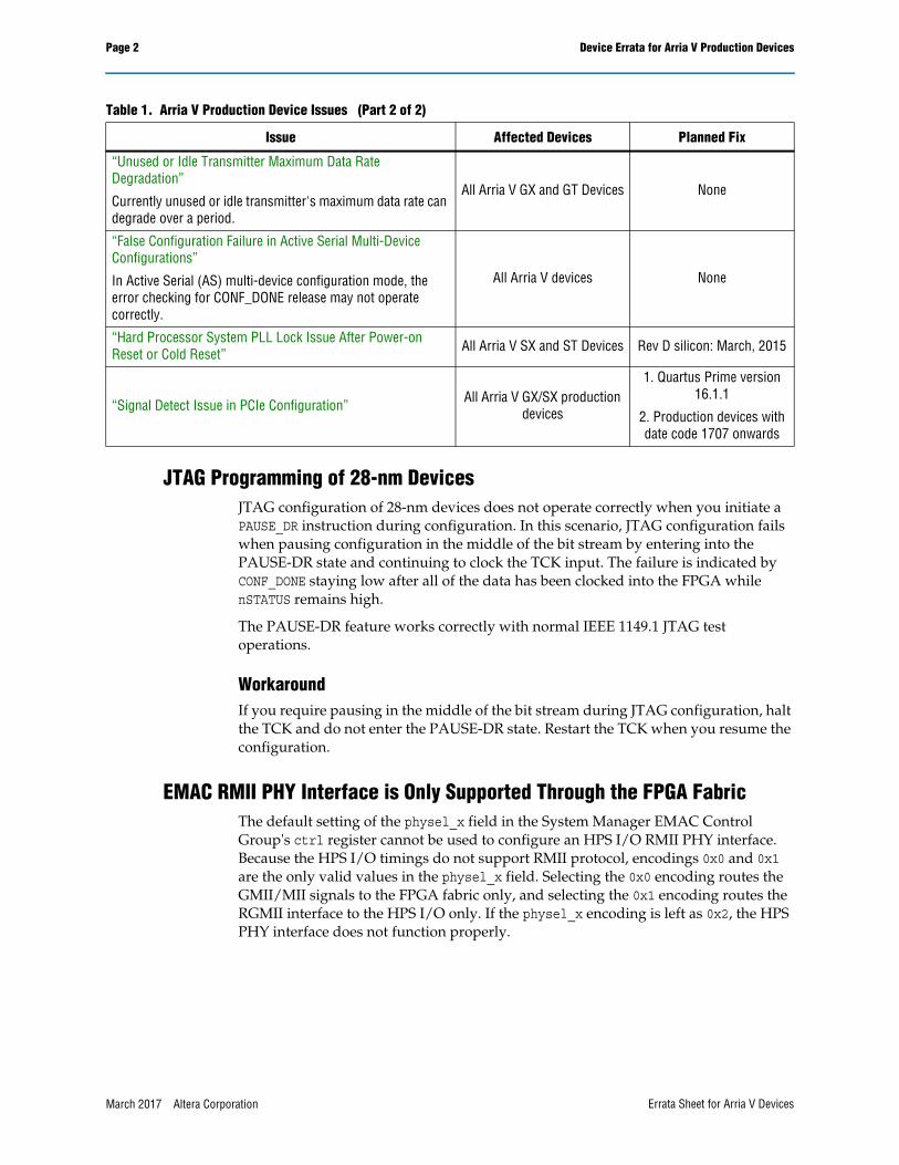
Page 2 Device Errata for Arria V Production Devices
March 2017 Altera Corporation Errata Sheet for Arria V Devices
JTAG Programming of 28-nm DevicesJTAG configuration of 28-nm devices does not operate correctly when you initiate a PAUSE_DR instruction during configuration. In this scenario, JTAG configuration fails when pausing configuration in the middle of the bit stream by entering into the PAUSE-DR state and continuing to clock the TCK input. The failure is indicated by CONF_DONE staying low after all of the data has been clocked into the FPGA while nSTATUS remains high.
The PAUSE-DR feature works correctly with normal IEEE 1149.1 JTAG test operations.
WorkaroundIf you require pausing in the middle of the bit stream during JTAG configuration, halt the TCK and do not enter the PAUSE-DR state. Restart the TCK when you resume the configuration.
EMAC RMII PHY Interface is Only Supported Through the FPGA FabricThe default setting of the physel_x field in the System Manager EMAC Control Group's ctrl register cannot be used to configure an HPS I/O RMII PHY interface. Because the HPS I/O timings do not support RMII protocol, encodings 0x0 and 0x1 are the only valid values in the physel_x field. Selecting the 0x0 encoding routes the GMII/MII signals to the FPGA fabric only, and selecting the 0x1 encoding routes the RGMII interface to the HPS I/O only. If the physel_x encoding is left as 0x2, the HPS PHY interface does not function properly.
“Unused or Idle Transmitter Maximum Data Rate Degradation”
Currently unused or idle transmitter's maximum data rate can degrade over a period.
All Arria V GX and GT Devices None
“False Configuration Failure in Active Serial Multi-Device Configurations”
In Active Serial (AS) multi-device configuration mode, the error checking for CONF_DONE release may not operate correctly.
All Arria V devices None
“Hard Processor System PLL Lock Issue After Power-on Reset or Cold Reset” All Arria V SX and ST Devices Rev D silicon: March, 2015
“Signal Detect Issue in PCIe Configuration” All Arria V GX/SX production devices
1. Quartus Prime version 16.1.1
2. Production devices with date code 1707 onwards
Table 1. Arria V Production Device Issues (Part 2 of 2)
Issue Affected Devices Planned Fix
Device Errata for Arria V Production Devices Page 3
March 2017 Altera CorporationErrata Sheet for Arria V Devices
WorkaroundIf an RMII PHY interface is required, the physel_x field should be set to 0x0 so that the GMII/MII signals are routed to the FPGA. You can design an RMII soft adaptor in the FPGA configuration file that converts these MII signals to an RMII PHY interface that is mapped to the FPGA I/O pins. Refer to the “Programming Model” section of the EMAC chapter in the Arria V Device Handbook, Volume 3: Hard Processor System Technical Reference Manual for more information about how to initialize the EMAC Controller and interface.
Hard Processor System Level 2 Cache Error Correction CodeAfter enabling the L2 cache ECC feature, false ECC errors may occur.
For affected devices, L2 cache ECC can be used and this issue avoided by setting the mpu_base_clk to a maximum frequency as follows:
■ Fast speed grade (-4) — 500 MHz
■ Mid speed grade (-5) — 400 MHz
■ Slow speed grade (-6) — 300 MHz
f If you are not using the L2 ECC feature, refer to the Arria V Device Datasheet for the maximum frequency of the mpu_base_clk.
Table 2 identifies the fixed silicon by die revision for each device.
Table 2. Device and Revision Fixed
Device Revision without Fix Revision with Fix
5ASXB3 Rev A & B Rev C
5ASXB5 Rev A & B Rev C
5ASTD3 Rev A & B Rev C
5ASTD5 Rev A & B Rev C
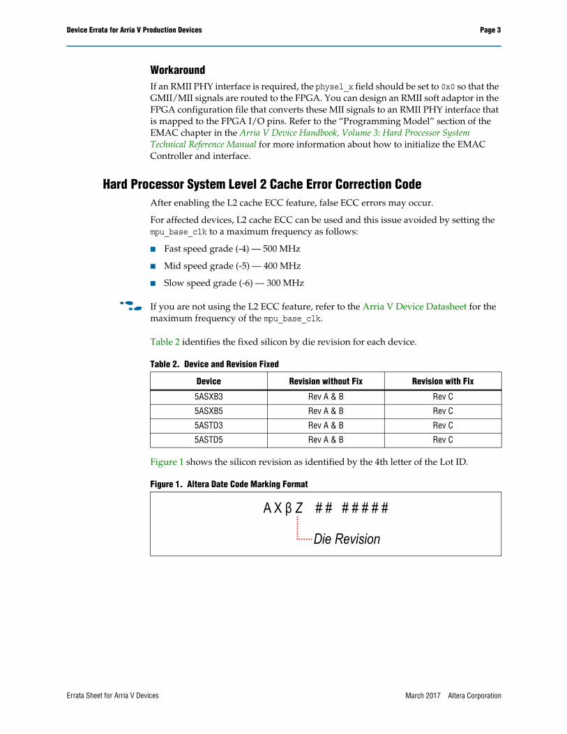
Figure 1 shows the silicon revision as identified by the 4th letter of the Lot ID.
Figure 1. Altera Date Code Marking Format
A X β Z # # # # # # #
Die Revision
Page 4 Device Errata for Arria V Production Devices
March 2017 Altera Corporation Errata Sheet for Arria V Devices
EMIF Maximum Frequency Specification UpdateTo achieve timing closure, the external memory interface (EMIF) maximum frequency specification has been updated.
Table 3. Arria V EMIF Maximum Frequency Specification Update (1), (2)
Device Speed Grade
Memory Type
Memory Topology
Depth Expansion
Interface Type
Original Maximum
Specifications (MHz)
Updated Maximum
Specifications (MHz)
Arria V GX C4 DDR2 Component 2 Chip Selects
Hard Controller 350 333
Arria V GX/GT I3 DDR2 Component 2 Chip
SelectsHard Controller 350 333
Arria V GX/GT I3 DDR3/
DDR3L Component 1 Chip Select Hard Controller 533 533 (3)
Notes to Table 3:
(1) The stated performances apply to component topology only. Hard controllers do not support DDR2 and DDR3 DIMM configurations.(2) For changes to other variants and slower speed grades, please refer to the External Memory Interface Spec Estimator.(3) Upgrade the DDR3 SDRAM/DDR3L SDRAM component from 533 MHz to 667 MHz to achieve the specified maximum frequency.
SolutionThese maximum frequency specifications have been updated in the External Memory Interface Spec Estimator.
SEU Internal ScrubbingThe SEU internal scrubbing feature has usage restrictions. For additional information, contact mySupport.
Fractional PLL Phase Alignment ErrorThe fPLL has a silicon sensitivity that causes the static phase error to operate beyond the Quartus® II software expectation. The frequency range and jitter performance of the fPLL meet the datasheet specification. This sensitivity is a time-zero failure, which means a design affected by this issue will show failure immediately upon a given device operation over expected operating conditions or will never show the issue.
The following usage modes may be affected:
■ When the fPLL is used for phase compensation. For example, applications that may use phase compensation include LVDS, board trace matching, or FPGA skew compensation, such as zero delay buffering.
■ Specific IP cores that require fPLL usage
■ Inter-clock domain transfers involving fPLL usage
WorkaroundCustomers can implement design techniques to mitigate inter-clock domain transfers and use the Altera® tool to evaluate fPLL usage and determine if designs may be affected by this issue.
Device Errata for Arria V Production Devices Page 5
March 2017 Altera CorporationErrata Sheet for Arria V Devices
f To determine if your design may be affected, use the Altera fPLL Usage Evaluation Tool.
If you believe your design is affected by this issue, please contact mySupport for further assistance.
Long-Term FixThis issue is, or will be fixed in the silicon die revision shown below. Table 4 identifies the fixed silicon by die revision for each device.
Table 4. Fixed Silicon by Die Revision
Family Device Fixed Die Revision
Arria V GT
5AGTD7 C
5AGTD3 D
5AGTC7 B
5AGTC3 B
Arria V GX
5AGXB7 C
5AGXB5 C
5AGXB3 D
5AGXB1 D
5AGXA7 B
5AGXA5 B
5AGXA3 B
5AGXA1 B
Arria V ST5ASTD5 B
5ASTD3 B
Arria V SX5ASXB5 B
5ASXB3 B
f For an explanation of the date code and revision marking format, refer to Figure 3 on page 9.
Page 6 Device Errata for Arria V Production Devices
March 2017 Altera Corporation Errata Sheet for Arria V Devices
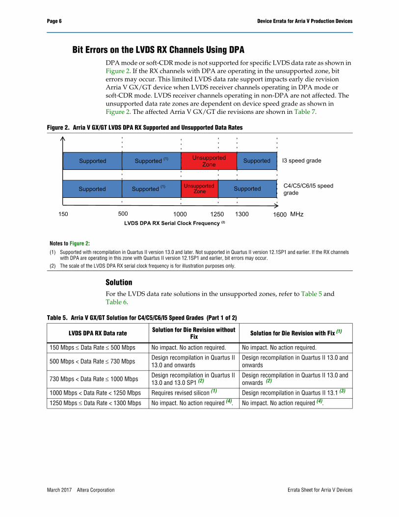
Bit Errors on the LVDS RX Channels Using DPADPA mode or soft-CDR mode is not supported for specific LVDS data rate as shown in Figure 2. If the RX channels with DPA are operating in the unsupported zone, bit errors may occur. This limited LVDS data rate support impacts early die revision Arria V GX/GT device when LVDS receiver channels operating in DPA mode or soft-CDR mode. LVDS receiver channels operating in non-DPA are not affected. The unsupported data rate zones are dependent on device speed grade as shown in Figure 2. The affected Arria V GX/GT die revisions are shown in Table 7.
Figure 2. Arria V GX/GT LVDS DPA RX Supported and Unsupported Data Rates
I3 speed grade
500 MHz LVDS DPA RX Serial Clock Frequency (2)
Supported Unsupported Zone
1300 MH1600
Supported
150 1250
Supported Unsupported Zone Supported
Supported (1)
Supported (1) C4/C5/C6/I5 speedgrade
1000
Notes to Figure 2:
(1) Supported with recompilation in Quartus II version 13.0 and later. Not supported in Quartus II version 12.1SP1 and earlier. If the RX channels with DPA are operating in this zone with Quartus II version 12.1SP1 and earlier, bit errors may occur.
(2) The scale of the LVDS DPA RX serial clock frequency is for illustration purposes only.
SolutionFor the LVDS data rate solutions in the unsupported zones, refer to Table 5 and Table 6.
Table 5. Arria V GX/GT Solution for C4/C5/C6/I5 Speed Grades (Part 1 of 2)
LVDS DPA RX Data rate Solution for Die Revision without Fix Solution for Die Revision with Fix (1)
150 Mbps Data Rate 500 Mbps No impact. No action required. No impact. No action required.
500 Mbps < Data Rate 730 Mbps Design recompilation in Quartus II 13.0 and onwards
Design recompilation in Quartus II 13.0 and onwards
730 Mbps < Data Rate 1000 Mbps Design recompilation in Quartus II 13.0 and 13.0 SP1 (2)
Design recompilation in Quartus II 13.0 and onwards (2)
1000 Mbps < Data Rate < 1250 Mbps Requires revised silicon (1) Design recompilation in Quartus II 13.1 (3)
1250 Mbps Data Rate < 1300 Mbps No impact. No action required (4). No impact. No action required (4).
Device Errata for Arria V Production Devices Page 7
March 2017 Altera CorporationErrata Sheet for Arria V Devices
1300 Mbps Data Rate 1600 Mbps No impact. No action required. No impact. No action required.
Notes to Table 5:
(1) The die revision for devices with fix is shown in Table 7.(2) The designs operating at these data rates compiled in Quartus II 13.0 and 13.0 SP1 support die revisions with and without fix, and no design
recompilation is required in Quartus II 13.1. The designs compiled in Quartus II 13.1 and onwards only support die revision with fix. Please contact mySupport for further assistance.
(3) Please contact mySupport for compilation support on the die revision with fix prior to Quartus II 13.1(4) The designs operating at these data rates compiled in Quartus II prior to 13.1 support die revisions with and without fix, and no design
recompilation is required in Quartus II 13.1. The designs compiled in Quartus II 13.1 and onwards only support die revision with fix. Please contact mySupport for further assistance.
Table 6. Arria V GX/GT Solution for I3 Speed Grade
Data rate Solution for Device Revision without Fix (1) Solution for Device Revision with Fix (1)
150 Mbps Data Rate 500 Mbps No impact. No action required. No impact. No action required.
500 Mbps < Data Rate 730 Mbps Design recompilation in Quartus II 13.0 and onwards
Design recompilation in Quartus II 13.0 and onwards
730 Mbps < Data Rate 1000 MbpsDesign recompilation in Quartus II 13.0 and 13.0 SP1 (2)
Design recompilation in Quartus II 13.0 and onwards (2)
1000 Mbps < Data Rate < 1250 Mbps Requires revised silicon (1) Design recompilation in Quartus II 13.1 (3)
1250 Mbps Data Rate < 1300 Mbps Requires revised silicon (1) Design recompilation in Quartus II 13.1 (3)
1300 Mbps Data Rate 1600 Mbps No impact. No action required. No impact. No action required.
Notes to Table 6:
(1) The die revision for devices with fix is shown in Table 7.(2) The designs operating at these data rates compiled in Quartus II 13.0 and 13.0SP1 support die revisions with and without fix, and no design
recompilation is required in Quartus II 13.1. The designs compiled in Quartus II 13.1 and onwards only support die revision with fix. Please contact mySupport for further assistance.
(3) Please contact mySupport for compilation support on the die revision with fix prior to Quartus II 13.1
Table 5. Arria V GX/GT Solution for C4/C5/C6/I5 Speed Grades (Part 2 of 2)
LVDS DPA RX Data rate Solution for Die Revision without Fix Solution for Die Revision with Fix (1)
Table 7. Arria V GX/GT Device Revision with Fix (Part 1 of 2)
Member code Revisions without Fix Revision with Fix (1)
5AGXA1 A B
5AGXA3 A B
5AGXA5 A B
5AGXA7 A B
5AGXB1 A, B, C D
5AGXB3 A, B, C D
5AGXB5 A, B C
5AGXB7 A, B C
5AGTC3 A B
5AGTC7 A B
5AGTD3 C D
Page 8 Device Errata for Arria V Production Devices
March 2017 Altera Corporation Errata Sheet for Arria V Devices
Dynamic Frequency Range Constraints for DPA and Soft-CDR ModeWhen LVDS receivers are implemented with dynamic frequency range, either with reconfigurable PLL, or via input frequency changes, the frequency range of the serial clock (fast clock) is limited to the following range (Table 8) in a single design compilation.
Table 8. Dynamic Frequency Range Constraints for DPA and Soft-CDR mode
Frequency Range Support for PLL Reconfiguration for LVDS Receivers with DPA (1) Device Revision without Fix Device Revision with Fix
150 Mbps Data Rate 500 Mbps Supported Supported
500 Mbps < Data Rate 730 Mbps Supported Supported
730 Mbps < Data Rate < 1300 Mbps Not supported Supported
1300 Mbps Data Rate 1600 Mbps Supported Supported
Note to Table 8:
(1) PLL reconfiguration or dynamic input frequency changes is only allowed within the defined range.
Please contact mySupport for further assistance.
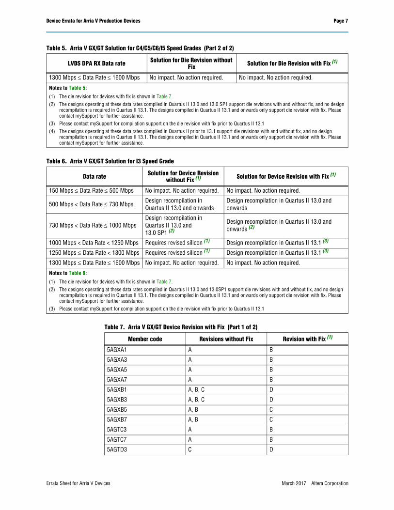
Configuration via Protocol (CvP)The fix involves a new die revision. You can use the die revision character in the Date Code to determine whether or not the device supports CvP.
CvP update can only be used at Gen1 data rates. CvP is supported if the fourth alphanumeric character (Z) from the left printed on the top side of the device is equal to or later in the alphabet than the letter shown in the Revision with Fix column of Table 9.
Figure 3 shows an Arria V device's top side date code.
5AGTD7 A, B C
Note to Table 7:
(1) Refer to Figure 3 for the Arria V device's top side data code. This issue is fixed if the fourth alphanumeric character (Z) from the left printed on the top side of the device is equal to or later in the alphabet than the letter shown in the Revision with Fix column.
Table 7. Arria V GX/GT Device Revision with Fix (Part 2 of 2)
Member code Revisions without Fix Revision with Fix (1)
Figure 3. Altera Date Code Marking Format
A X β Z # # # # # # #
Die Revision
Table 9. Device and Die Revisions
Member Code Revisions without Fix Revision with Fix
5AGXA1 A B
5AGXA3 A B
5AGXA5 None A
5AGXA7 None A
5AGXB1 A, B and C D
5AGXB3 A, B and C D
5AGXB5 A and B C
5AGXB7 A and B C
5AGTC3 A B
5AGTC7 None A
5AGTD3 A, B and C D
5AGTD7 A and B C
5ASXB3 None A
5ASXB5 None A
5ASTD3 None A
5ASTD5 None A
Note to Table 9:
Future revisions (not shown in the table above) will be CvP capable.
Device Errata for Arria V Production Devices Page 9
March 2017 Altera CorporationErrata Sheet for Arria V Devices
For Gen2 CvP update or further inquiries, please contact mySupport.
Partial Reconfiguration (PR) with Compression Feature Not SupportedThe Partial Reconfiguration (PR) with CvP is not supported when compression is turned on and encryption is turned off. There is no restriction when CvP is disabled. Table 10 shows the support of PR with CvP in different states of compression and encryption.
Table 10. PR Support with CvP in Various States of Compression and Encryption
Compression with PR Encryption with PR CvP mode Support
OFF OFF On Yes
OFF ON On Yes
ON OFF On No
ON ON On Yes
Page 10 Device Errata for Arria V Production Devices
March 2017 Altera Corporation Errata Sheet for Arria V Devices
Please contact mySupport for further assistance.
Usermode High IccWhen the affected device transitions into User mode, high Icc is observed, due to internal dataline contention.
WorkaroundUse the following software workaround to prevent the user mode high Icc issue:
■ For the Error Detection Cyclic Redundancy Check (EDCRC) user, no workaround is needed because the EDCRC feature eliminates the high Icc issue.
■ For the non-EDCRC user, a software workaround is needed and is available in the Quartus II software version 12.1 sp1, or later.
Action Needed for Existing Designs (pre-Quartus II software version 12.1 sp1)Specific action is needed when the existing design uses the EDCRC and certain versions of the Quartus II software. Table 11 lists the actions needed for the different settings.
Table 11. Action for Existing Designs
Design Quartus II Version Action
EDCRC enabled. Any None needed.
EDCRC disabled12.1 only Full recompilation is required using the Quartus II software version 12.1 sp1,
or later release.
Pre 12.1 Full recompilation is NOT needed, but requires the use of Quartus II software version 12.1 sp1, or later for programming file conversion (1).
Note to Table 11:
(1) Convert the existing SOF file to RBF, POF, JIC, or another format using Convert Programming File, under the File menu of the Quartus II software.
Unused or Idle Transmitter Maximum Data Rate DegradationA currently unused or idle transmitter's maximum data rate can degrade over a period. The issue is caused by degradation in the local or central clock divider (used to drive the transmitter) being left idle over an extended period, with the transceiver's power supplies powered up.
Device Errata for Arria V Production Devices Page 11
March 2017 Altera CorporationErrata Sheet for Arria V Devices
The issue only impacts designs that will enable unused or idle transmit channels with idling clock dividers through a new programming file at a later date. The transmit channel in devices that do not power up the transceiver power supplies are not affected.
The idling clock divider can occur in three conditions:
1. Transmit channels in permanent reset
a. Transmit channels that will be enabled later are instantiated in the current design, but with the PMA block or divider source clock (CMU PLL or fPLL) held in reset permanently.
2. Unused non-bonded transmit channels
a. Non-bonded transmit channels that will be enabled later are not instantiated in the current design, resulting in an idling local clock divider.
3. Unused CMU PLL or fPLL for bonding
a. CMU PLL or fPLL used for bonding that will be enabled later are not instantiated in the current design, resulting in an idling central clock divider.
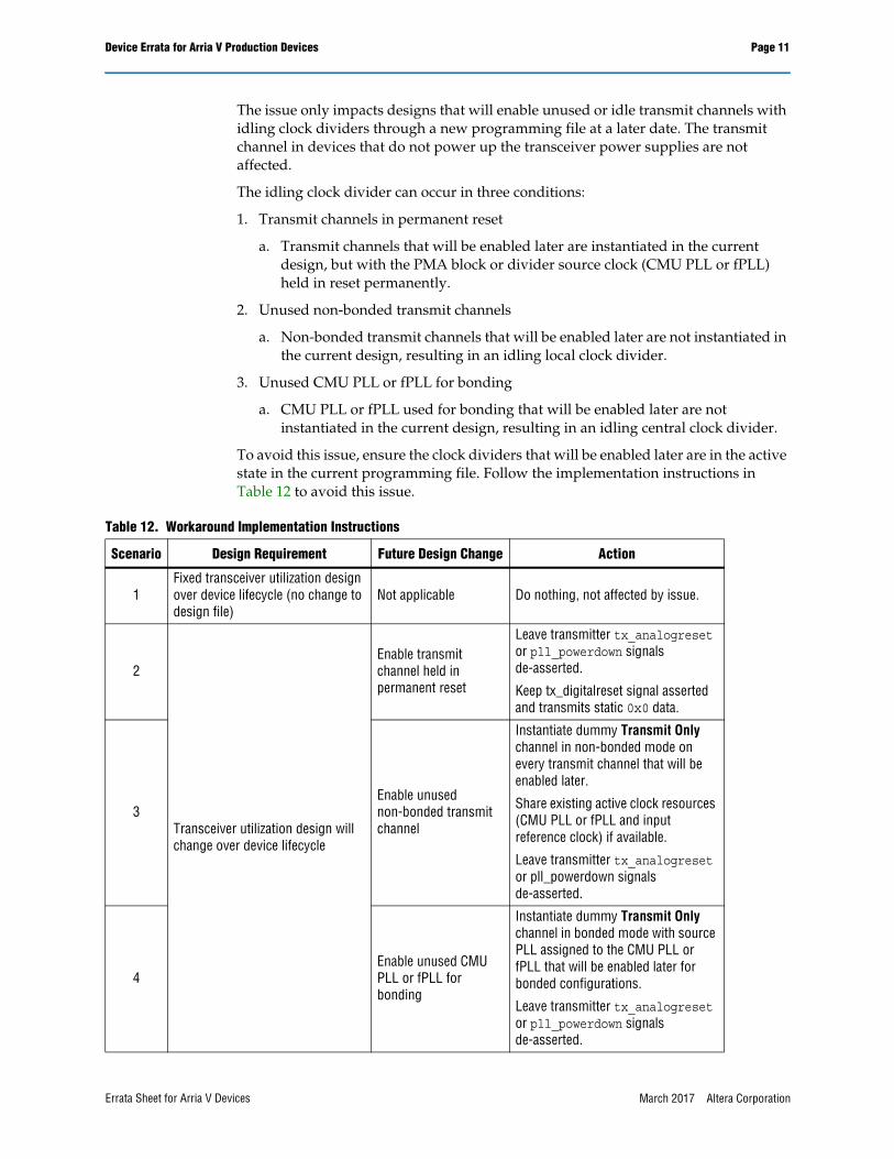
To avoid this issue, ensure the clock dividers that will be enabled later are in the active state in the current programming file. Follow the implementation instructions in Table 12 to avoid this issue.
Table 12. Workaround Implementation Instructions
Scenario Design Requirement Future Design Change Action
1Fixed transceiver utilization design over device lifecycle (no change to design file)
Not applicable Do nothing, not affected by issue.
2
Transceiver utilization design will change over device lifecycle
Enable transmit channel held in permanent reset
Leave transmitter tx_analogreset or pll_powerdown signals de-asserted.
Keep tx_digitalreset signal asserted and transmits static 0x0 data.
3Enable unused non-bonded transmit channel
Instantiate dummy Transmit Only channel in non-bonded mode on every transmit channel that will be enabled later.
Share existing active clock resources (CMU PLL or fPLL and input reference clock) if available.
Leave transmitter tx_analogreset or pll_powerdown signals de-asserted.
4Enable unused CMU PLL or fPLL for bonding
Instantiate dummy Transmit Only channel in bonded mode with source PLL assigned to the CMU PLL or fPLL that will be enabled later for bonded configurations.
Leave transmitter tx_analogreset or pll_powerdown signals de-asserted.
Page 12 Device Errata for Arria V Production Devices
March 2017 Altera Corporation Errata Sheet for Arria V Devices
1 The dummy Transmit Only channel will increase transceiver power consumption in your design. Use the Early Power Estimator (EPE) tool or PowerPlay Power Analyzer (PPPA) in the Quartus II software to account for the power increase from the additional dummy channels.
Use the following general guidelines for reducing power consumed by the dummy Transmit Only channel:
1. In Arria V GT devices, instantiate the dummy channel in PMA direct mode with Native PHY IP.
2. In Arria V GX devices, keep the tx_digitalreset signal asserted in dummy channel to minimize PCS activity.
3. Transmit the static 0x0 data over dummy channel.
4. Configure the dummy channel with the lowest possible data rate.
5. Set the VOD = 6 (minimum value) on the transmitter output pin for dummy channel.
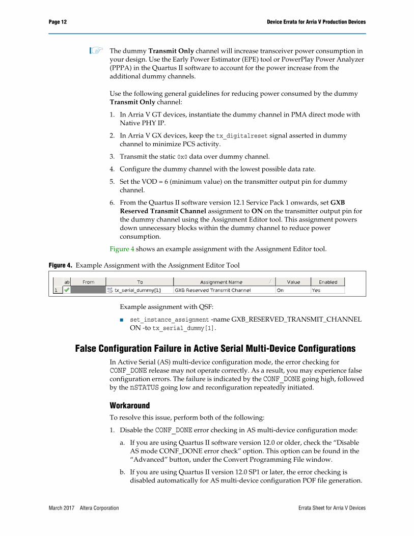
6. From the Quartus II software version 12.1 Service Pack 1 onwards, set GXB Reserved Transmit Channel assignment to ON on the transmitter output pin for the dummy channel using the Assignment Editor tool. This assignment powers down unnecessary blocks within the dummy channel to reduce power consumption.
Figure 4 shows an example assignment with the Assignment Editor tool.
Figure 4. Example Assignment with the Assignment Editor Tool
Example assignment with QSF:
■ set_instance_assignment -name GXB_RESERVED_TRANSMIT_CHANNEL ON -to tx_serial_dummy[1].
False Configuration Failure in Active Serial Multi-Device ConfigurationsIn Active Serial (AS) multi-device configuration mode, the error checking for CONF_DONE release may not operate correctly. As a result, you may experience false configuration errors. The failure is indicated by the CONF_DONE going high, followed by the nSTATUS going low and reconfiguration repeatedly initiated.
WorkaroundTo resolve this issue, perform both of the following:
1. Disable the CONF_DONE error checking in AS multi-device configuration mode:
a. If you are using Quartus II software version 12.0 or older, check the “Disable AS mode CONF_DONE error check” option. This option can be found in the “Advanced” button, under the Convert Programming File window.
b. If you are using Quartus II version 12.0 SP1 or later, the error checking is disabled automatically for AS multi-device configuration POF file generation.
Device Errata for Arria V Production Devices Page 13
March 2017 Altera CorporationErrata Sheet for Arria V Devices
2. Enable the INIT_DONE pin option:
a. To ensure a successful configuration, Altera recommends that you enable the INIT_DONE optional pin for devices in the configuration chain. On the board, route out the INIT_DONE pin separately for both the master and slave devices. Monitor the INIT_DONE status for each of the devices to ensure a successful transition into User-mode.
1 Other configuration modes (JTAG, Fast Passive Parallel (FPP), and Passive Serial (PS) (single and multi device configurations, and AS single-device configurations) are not affected.
Hard Processor System PLL Lock Issue After Power-on Reset or Cold ResetOne or more of the PLLs in the hard processor system (HPS) of Arria V SoC devices can take a long time to lock after power-on reset or cold reset. This occurs when the clock select (CSEL) pins are set to 01, 10, or 11. Some peripherals clocked by the HPS PLLs may fail to operate properly. While this failure is rare, typical symptoms include:
■ The HPS hangs during the Boot ROM stage and is unable to proceed to the Preloader stage.
■ An intermittent SDRAM calibration error in the Preloader.
WorkaroundThese issues can be resolved by implementing the following changes:
1. Connect the CSEL pins [1:0] to pull down resistors (4.7 k to 10 k) on the board to force the CSEL input to be 0.
2. Download and install the appropriate SoCEDS patch for software version 13.1 or 14.0. Then, recompile the Preloader code.
To download and install the required SoCEDS patch for SoCEDS version 13.1 and 14.0, refer to KDB solution rd06202014. Software in the patch is integrated into SoCEDS version 14.0.1.
Selecting CSEL=00 causes the Boot ROM to bypass the PLLs on cold reset, instead using the external clock input (osc_1_clk) for the peripheral interfaces. Because the external clock is already stable, using it ensures the Preloader code loads properly from external Flash.
The software patch adds code to the Preloader, which locks the PLLs quickly, which in turn resolves the intermittent SDRAM calibration issue. It also loads a piece of code into the on-chip RAM to handle a warm reset. Clocks are handled differently depending on whether the reset is warm or cold.
Workaround Implications
Bypassing the PLLs after cold reset increases the boot time slightly because the external clock is slower than the Flash interface clock generated from the HPS peripheral PLL.
Altera reserves the upper 4 KB of on-chip RAM for the warm boot code.
Page 14 Device Errata for Arria V Production Devices
March 2017 Altera Corporation Errata Sheet for Arria V Devices
1 Do not overwrite the content of the upper 4 KB of the address range in the on-chip RAM. If you need a smaller memory footprint for the code, file a service request using mySupport.
The on-chip memory restriction can be eliminated entirely if the SoC warm and cold reset pins are tied together, or if the HPS boots from FPGA memory.
Device and Revision Fixed
Table 13 identifies the fixed silicon by die revision for each device.
Table 13. Device and Revision Fixed
Device Revision Without Fix Revision With Fix
5ASXB3 Rev C Rev D
5ASXB5 Rev C Rev D
5ASTD3 Rev C Rev D
5ASTD5 Rev C Rev D
Figure 5 shows the silicon revision as identified by the 4th letter of the Lot ID.
Figure 5. Altera Date Code Marking Format
A X β Z # # # # # # #
Die Revision
Signal Detect Issue in PCIe ConfigurationThe Signal Detect (SD) circuit required in the PCIe configuration (Hard IP and PIPE mode) may switch OFF for both of the following conditions:
■ Low temperature
■ Upper limit of VCCER_GXB (receiver buffer power supply voltage)
PCIe link training may not be fully completed in the case where the SD circuit remains de-asserted or OFF with an incoming signal.
This issue is a time-zero condition. If shipped devices have been tested and do not exhibit this issue, it will not occur in the future.
WorkaroundPerform the following procedure:
Document Revision History Page 15
March 2017 Altera CorporationErrata Sheet for Arria V Devices
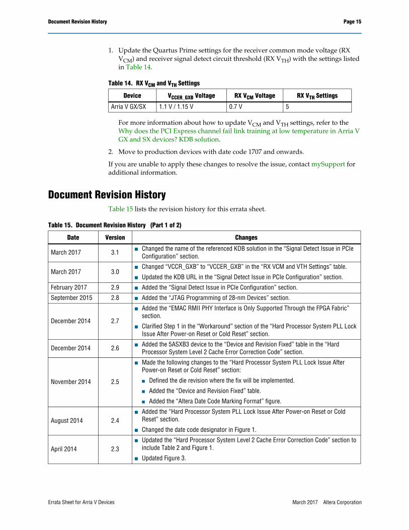
1. Update the Quartus Prime settings for the receiver common mode voltage (RX VCM) and receiver signal detect circuit threshold (RX VTH) with the settings listed in Table 14.
Table 14. RX VCM and VTH Settings
Device VCCER_GXB Voltage RX VCM Voltage RX VTH Settings
Arria V GX/SX 1.1 V / 1.15 V 0.7 V 5
For more information about how to update VCM and VTH settings, refer to the Why does the PCI Express channel fail link training at low temperature in Arria V GX and SX devices? KDB solution.
2. Move to production devices with date code 1707 and onwards.
If you are unable to apply these changes to resolve the issue, contact mySupport for additional information.
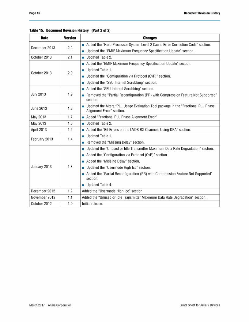
Document Revision HistoryTable 15 lists the revision history for this errata sheet.
Table 15. Document Revision History (Part 1 of 2)
Date Version Changes
March 2017 3.1 ■ Changed the name of the referenced KDB solution in the “Signal Detect Issue in PCIe Configuration” section.
March 2017 3.0■ Changed “VCCR_GXB” to “VCCER_GXB” in the “RX VCM and VTH Settings” table.
■ Updated the KDB URL in the “Signal Detect Issue in PCIe Configuration” section.
February 2017 2.9 ■ Added the “Signal Detect Issue in PCIe Configuration” section.
September 2015 2.8 ■ Added the “JTAG Programming of 28-nm Devices” section.
December 2014 2.7
■ Added the “EMAC RMII PHY Interface is Only Supported Through the FPGA Fabric” section.
■ Clarified Step 1 in the “Workaround” section of the “Hard Processor System PLL Lock Issue After Power-on Reset or Cold Reset” section.
December 2014 2.6 ■ Added the 5ASXB3 device to the “Device and Revision Fixed” table in the “Hard Processor System Level 2 Cache Error Correction Code” section.
November 2014 2.5
■ Made the following changes to the “Hard Processor System PLL Lock Issue After Power-on Reset or Cold Reset” section:
■ Defined the die revision where the fix will be implemented.
■ Added the “Device and Revision Fixed” table.
■ Added the “Altera Date Code Marking Format” figure.
August 2014 2.4■ Added the “Hard Processor System PLL Lock Issue After Power-on Reset or Cold
Reset” section.
■ Changed the date code designator in Figure 1.
April 2014 2.3■ Updated the “Hard Processor System Level 2 Cache Error Correction Code” section to
include Table 2 and Figure 1.
■ Updated Figure 3.
Page 16 Document Revision History
March 2017 Altera Corporation Errata Sheet for Arria V Devices
December 2013 2.2■ Added the “Hard Processor System Level 2 Cache Error Correction Code” section.
■ Updated the “EMIF Maximum Frequency Specification Update” section.
October 2013 2.1 ■ Updated Table 2.
October 2013 2.0
■ Added the “EMIF Maximum Frequency Specification Update” section.
■ Updated Table 1.
■ Updated the “Configuration via Protocol (CvP)” section.
■ Updated the “SEU Internal Scrubbing” section.
July 2013 1.9■ Added the “SEU Internal Scrubbing” section.
■ Removed the “Partial Reconfiguration (PR) with Compression Feature Not Supported” section.
June 2013 1.8 ■ Updated the Altera fPLL Usage Evaluation Tool package in the “Fractional PLL Phase Alignment Error” section.
May 2013 1.7 ■ Added “Fractional PLL Phase Alignment Error”
May 2013 1.6 ■ Updated Table 2.
April 2013 1.5 ■ Added the “Bit Errors on the LVDS RX Channels Using DPA” section.
February 2013 1.4■ Updated Table 1.
■ Removed the “Missing Delay” section.
January 2013 1.3
■ Updated the “Unused or Idle Transmitter Maximum Data Rate Degradation” section.
■ Added the “Configuration via Protocol (CvP)” section.
■ Added the “Missing Delay” section.
■ Updated the “Usermode High Icc” section.
■ Added the “Partial Reconfiguration (PR) with Compression Feature Not Supported” section.
■ Updated Table 4.
December 2012 1.2 Added the “Usermode High Icc” section.
November 2012 1.1 Added the “Unused or Idle Transmitter Maximum Data Rate Degradation” section.
October 2012 1.0 Initial release.
Table 15. Document Revision History (Part 2 of 2)
Date Version Changes