Embed Size (px)
Citation preview
CVD POLYCRYSTALLINE DIAMOND (POLY-C) THIN FILM TECHNOLOGY FOR MEMS PACKAGING
By
Xiangwei Zhu
A DISSERTATION
Submitted to Michigan State University
in partial fulfillment of the requirements for the degree of
DOCTOR OF PHILOSOPHY
Department of Electrical and Computer Engineering
2006
ABSTRACT CVD POLYCRYSTALLINE DIAMOND (POLY-C) THIN FILM TECHNOLOGY
FOR MEMS PACKAGING
By
Xiangwei Zhu
Poly-crystalline diamond (poly-C), with unique mechanical, thermal,
chemical and electrical properties, is an excellent material for
MicroElectroMechanicalSystems (MEMS) and its packaging applications. The
research reported in this dissertation focuses on the investigation of applications
of CVD poly-C technology in the area of MEMS packaging.
MEMS design is quite application-specific. Therefore, it is important to
couple the packaging design closely with MEMS design. Tremendous research
efforts have been exerted on the studies of various packaging technologies,
which can be classified as wafer bonding process, encapsulation process and 3-
D multi-chip-module assembly. In addition to improve conventional MEMS
packaging technologies, there is also a growing interest to explore the
applications of new material technologies on MEMS packaging. Recently, poly-C
has emerged as a novel material for MEMS applications on both micro device
and packaging.
In this research work, fundamental researches on poly-C thin film
techniques, such as seeding, CVD deposition and doping, have been performed
for the purpose of characterization and improvement. Then, several enabling
techniques have been developed, including poly-C microstructure fabrication,
ultra-fast diamond growth model, poly-C panel with built-in interconnects and
diamond-diamond CVD bonding. Based on all these techniques, a poly-C thin
film encapsulation packaging process which can be intenerated with MEMS
device fabrication process has been developed.
This poly-C thin film packaging technology has been used to encapsulate
poly-C cantilever resonator, to evaluate the efficacy of poly-C encapsulation.
Poly-C cantilever beam resonators were tested using piezoelectric actuation and
laser detection method before and after poly-C packaging process. Resonance
frequencies measured before and after are in the range of 240-320 KHz, which is
consistent with theoretical calculations. The application of diamond for thin film
package is being reported for the first time.
iv
ACKNOWLEDGEMENTS
The author wishes to thank his advisor, Dr. Dean M. Aslam, for his
encouragement, guidance and support throughout this research. Additional
thanks are extended to Dr. Donnie K. Reinhard, Dr. Tim Hogan, Dr. Ahmed M.
Naguib and Dr. Khalil Najafi for their valuable discussions and academic advices.
The author would like to thank all the members of Dr. Aslam’s research
group, Ungsik Kim, Yuxing Tang, Yang Lu and Nelson Sepulveda, for their
assistance and helpful discussions. The author is also thankful to Dr. Brian Stark
and Warren Welch of University of Michigan for cooperation.
Last but not least, the author would like to thank his family in China and his
wife, Liling Jiang, for their patience, understanding and sacrifice during the
course of this study.
This work was supported primarily by the Engineering Research Centers
Program of the National Science Foundation under Award Number EEC-
9986866.
v
TABLE OF CONTENTS
LIST OF TABLES………………………………………………………….…………..viii
LIST OF FIGURES……………………………………………………………………ix
1. RESEARCH MOTIVATION AND GOALS 1.1 Introduction……………………………………….………………………….1 1.2 Objective of This Work…………………………………….………………..3 1.3 Dissertation Organization………………………………………………….5 2. BACKGROUND 2.1 Introduction……………………………………………………………….…7 2.2 MEMS Packaging Overview………………………………………………7 2.3 MEMS Packaging Approaches…………………………………………13
2.3.1 Wafer-bonding packaging process…………………………...14 2.3.2 Integrated encapsulation process…………………………….20 2.3.3 3-D multi-chip packaging approaches………………………….25
2.4 Diamond Properties………………………………………………….…29 2.5 CVD Diamond Deposition Techniques…………………………………33
2.5.1 CVD poly-C growth mechanism…………………………….…33 2.5.2 CVD poly-C deposition methods……………………………35
2.6 Poly-C MEMS Technology And Its Packaging Applications…………37 3. FUNDAMENTAL RESEARCH ON CVD POLY-C TECHNOLOGY
3.1 Introduction………………………………………………………………...42 3.2 Fabrication and Characterization Systems……………………………..42 3.2.1 MPCVD diamond deposition system………………………..43 3.2.2 Characterization systems……………………………… ..46 3.3 Basic Poly-C Technology……………………………………….………48 3.3.1 Diamond seeding technology.........................................48
3.3.1.1 Preparation of diamond seeds solution…………..49 3.3.1.2 Diamond seeding set-ups………………………...50 3.3.1.3 Characterization of seeding techniques…………..52
3.3.2 MPCVD poly-C deposition……………………….…………...57 3.3.2.1 Characterization of typical deposition parameters.58 3.3.2.2 Study of MPCVD deposition rate…………………...59
vi
3.3.2.3 Study of MPCVD grown poly-C film quality……...60 3.3.2.4 Study of low temperature poly-C deposition……...63
3.3.3 Diamond doping technology…………………………………….64 3.3.3.1 Resistivity measurement of doped poly-C thin film.65 3.3.3.2 Resistivity variation with doping and temperature...67
3.3.4 Patterning of poly-C.…………………………………………69
4. POLY-C ENABLING TECHNOLOGIES FOR MEMS PACKAGING 4.1 Introduction………………………………………………………………...73 4.2 Fabrication Techniques for Poly-C MEMS Structure………….………73
4.2.1 Poly-C plasma ECR dry-etching technique………….………74 4.2.2 Selective poly-C growth technique……..……….………76 4.2.2 High aspect ratio poly-C microstructure fabrication technique..77
4.3 Thick Poly-C Film Fabrication for MEMS Applications………………79 4.3.1 Ultra-fast poly-C growth model.…………….……………….….80 4.3.2 Double-side poly-C growth on DRIE etched Si mold………...81 4.3.3 Filing of silicon mold………………………………………………84 4.3.4 Fabrication of poly-C panel with built-in interconnects………85 4.4 Diamond-diamond Bonding Technology……………………..…….91
5. POLY-C THIN FILM ENCAPSULATION PACKAGING 5.1 Introduction……………………………………………………………….92 5.2 Poly-C Thin Film Packaging Process Design……………….………93
5.2.1 Packaging material selection……………………….…………94 5.2.2 Packaging process design………………………….…………97
5.3 Fabrication of Poly-C Package……………………………………….98 5.3.1 Poly-C thin film fabrication for packaging……….…………98 5.3.2 Poly-C thin film package………………………………………100 5.3.2 Fabrication of embedded feedthroughs………………………102 5.4 Evaluation of Poly-C Encapsulation Packaging Technology………..104 5.4.1 Corrosion-resistant test of poly-C package…………………..104 5.4.2 Poly-C encapsulation package for cantilever resonator….108
5.4.2.1 Piezoelectric actuation and laser detection for resonator measurement……………..………………108 5.4.2.2 Process integration and test chip fabrication………..110 5.4.2.3 Thin film package evaluation………………..……...113
6. CONCLUSIONS AND FUTURE RESEARCH 6.1 Summary and Conclusions…………………………………………….116
vii
6.2 Future Research Topics…………………………………………………117
APPENDIX A………………………………………………………………………119
APPENDIX B………………………………………………………………………120
APPENDIX C………………………………………………………………………121
BIBLIOGRAPHY……………………………………………………….…………….124
viii
LIST OF TABLES
2.1: Comparisons of packaging issues between MEMS/Microsystems and
Mic roe lec t ron i cs … … … … … … … … … … … … … … … … … … … … …8
2.2: Typical Materials used in MEMS..…………………………………………...13
2.3: Eutectic alloys for wafer bonding………………………………………….19
2.4: Common properties of diamond………………………………………………32
2.5: Comparison of different poly-C deposition methods………………………36
2.6: Comparison of different diamond dry etching techniques…………………39
3.1: Diamond seeding solution preparation…………………………………….49
3.2: Substrate pretreatment conditions and diamond growth time………….54
3.3: Comparison of different seeding methods…………………………………57
3.4: Typical poly-C deposition parameters of MPCVD……………………….…59
3.5: Correction factors of some finite thickness and diameters………………....67
4.1: ECR plasma etching parameters……………………………………………..75
4.2: Fabrication time of ultra-fast growth model………………………………..82
5.1: Properties of common thin film materials……………………………………96
5.2: Poly-C resonator parameters relevant to evaluating of poly-C package...115
ix
LIST OF FIGURES
1.1: Overview of CVD poly-C thin film technology for MEMS packaging………4 2.1: Schematic flow-chart for MEMS device and package design……….…….10 2.2: (a) Set-up of anodic silicon-glass bonding; (b) formation of anodic silicon -
glass bonding………………………………………………………………..16 2.3: Silicon fusion bonding set-up…………………………………………………18 2.4: Eutectic bonding set up……………………………………………………….20 2.5: Typical fabrication steps of integrated encapsulation………….…………..21 2.6: (a) An SEM microphoto of a vacuum-encapsulated lateral microresonator;
(b) Shell and freestanding comb structure cross section as seen in an SEM…………………………………………………………………………22
2.7: An integrated encapsulation process for a micro vacuum diode……….…23 2.8: SEM of a thin-film nickel package for Pirani gauge……………….………..24 2.9: A generic schematic diagram of an MCM architecture…………….………26 2.10: (a) a schematic diagram of system integration; (b) an integrated WIMS
cube………………………………………………………………………………28 2.11: Unit cell of diamond lattice……………………………………………………30 2.12: Band structure including exchange and correlation effects…..……………30 2.13: Schematic diagram of CVD diamond process…..…………………………34 2.14: Diamond replicas of etched Si molds….……………………………………38
x
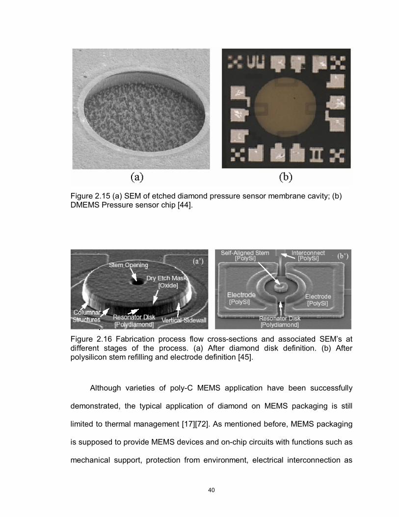
2.15: (a) SEM of etched diamond pressure sensor membrane cavity; (b) DMEMS Pressure sensor chip……………………………………………………40
2.16: Fabrication process flow cross-sections and associated SEM’s at different
stages of the process. (a) After diamond disk definition. (b) After polysilicon stem refilling and electrode definition….……………………………………40
3.1: Schematic diagram of MPCVD system…………..…………………….…...44 3.2: DPR / DW spin-on seeding setup……….…………………………….……..51 3.3: Electrophoresis setup………………………………………………………..51 3.4: Diamond Seeding Density vs. Spinning speeds……………………………52 3.5: Typical diamond seeding results: (a) DPR seeding density of 4 x 108 cm-2;
(b) DW seeding density of 5.6 x 109 cm-2…………………………………..53 3.6: SEM of the nucleation density for a) ultrasonication and electrophoresis
(sample 1); b) ultrasonication alone (sample 2); and c) electrophoresis alone (sample 3)………………………………………………………………..54
3.7: AFM of the nucleation density for (a) ultrasonication and electrophoresis
(sample 1); (b) ultrasonication alone (sample 2); and (c) electrophoresis alone (sample 3) with image of clumping (inset)……………………………55
3.8: Deposition rate variations with temperature…………………………….....61 3.9: Deposition rate variations with gas concentrations………………………..61 3.10: Raman spectra of poly-C films grown at different temperatures….….…..62 3.11: Two poly-C films grown at low temperature: (a) 475 ºC and (b) 550 ºC…63 3.12: Four point probe measurement setup..……………………………….……..65 3.13: Doped poly-C film resistivity versus TMB/CH4 ratio………………………...68 3.14: Temperature dependence of poly-C film resisitivity..………..……………69
xi
3.15: Lift-off patterning process………………………………..…………………...70 3.16: Schematic diagram of DPR patterning process…………….………….71 3.17: Schematic diagram of dry-etch patterning process…………….………….72 4.1: SEM picture of a poly-C crab-leg accelerometer patterned using dry-etching
technique; inset is a close view of etched edge………………….…………75 4.2: Selective poly-C growth process……………………………………………..76 4.3: SEM pictures of selectively grown poly-C microstructures: (a) channel
pattern, and (b) well pattern………………………………………………….77 4.4: Fabrication process; (a) - (c) Si mold fabrication using DRIE, (d) diamond
seeding, (e) poly-C deposition, (f) freestanding poly-C……………………78 4.5: Diamond seeding results; (a) uniform seeding, (b) nucleation density of
1.5x1010 cm-2, (c) & (d) seeding inside hannels……..………………………79 4.6: Freestanding poly-C microstructures; (a) 2 µm channels, (b) 4 µm channels,
(c) 10 µm channels, (d) 20 µm wells………………………………….….…..79 4.7: Ultra-fast growth model; (a) first poly-C deposition, (b) second poly-C
deposition…………………………………..…………………………………...80 4.8: 20–35 µm thick diamond films fabricated by ultra-fast method using; (a) 2
µm channels, (b) 6 µm channels, (c) 10 µm channels, (d) 10 µm wells array……………………………………………………………………..…83
4.9: Comparison of experimental and theoretical values of (1+ Aspect Ratio)..83 4.10: Filling properties in channels with different aspect ratio: (a) a channel with
aspect ratio 2, totally filled; (b) a channel with aspect ratio 3, totally filled; (c) a channel with aspect ratio 4, void formed; (d) a channel with aspect ratio 5, void formed……………………………………………………………………..85
4.11: Fabrication process of built-in interconnects……………………………....86
xii
4.12: SEM image of poly-C panel with built-in interconnects: (a) poly-C panel
before dry etching; (b) poly-C panel after dry etching; (c) top view of poly-C panel; (d) side view of poly-C panel………………………………..……….87
4.13: Surface micromachining process of built-in interconnects……..…………..88 4.14: Surface micromachined poly-C film with doped poly-C pattern.…………89 4.15: Poly-C resistivities for 1μm thick films deposited at 700 ºC. The inset shows
resistivity data from an earlier study (annealing temperature is 600 ºC)….90 4.16: Bonding process concept of poly-C films; (a) before and (b) after poly-C
bonding…………………………………………………………………………..92 4.17: SEM images of two bonded poly-C films using boding concept shown in
Figure 4.16………………………………………………...…………………...92 5.1: Basic concept of poly-C thin film Package: (a) complete package, and (b)
cross section view of package…………………………………………….…..95
5.2: Poly-C thin- film package fabrication process……..……………………….97
5.3: (a) Poly-C film surface; (b) Raman spectrum of poly-C film……………...99 5.4: Fabricated poly-C thin film package; insets are close view of (a) package
border, (b) anchor and access port, (c) close view of package anchor, and close view of access port: (d) before sealing, (e) after sealing.....………101
5.5: A broken poly-C thin film package….........................................................102 5.6: The fabrication of embedded feedthroughs: (a) doped poly-C and (b) poly-
s i l i con……………………………… . .…………………………………103 5.7: Fabrication process of corrosion-resistance test chip…………………….105 5.8: (a) Cross-section view of PECVD oxide layer; (b) Top view of a test
chip…………………………………………………………………………106
xiii
5.9: (a) Sample chip before soak test; (b) Sample chip after 3 weeks soak; (c) sample chip after 6 weeks soak…………….…………………………...….107
5.10: Schematic diagram of the piezoelectric actuation and laser detection setup…………………………………………………………..……….…109
5.11: Integrated poly-C thin fi lm encapsulation process for cantilever resonators…………………………………………………………………111
5.12: Fabricated poly-C cantilever resonators…………………………………….112
5.13: Fabricated poly-C thin film package; (a) release package before final sealing, (b) completely sealed package………………………………….…112
5.14: Encapsulated poly-C cantilever resonator……………..………………113 5.15: Measured frequency spectrums of (a) pre- and (b) post-packaging
samples…………………………………………….………………..………115
1
Chapter 1
Research Motivation and Goals
1.1 Introduction
MEMS packaging is a major challenge to Microsystems industries.
Although MEMS fabrication uses process and tools borrowed from
microelectronic industries with modification, MEMS design is quite different from
its microelectronic counterpart. MEMS design is so application-specific that every
specific device function plays an important role in package design consideration.
For example, resonant device such as RF filter might require vacuum packaging
while accelerometers might work better at atmospheric pressure. This makes the
development of packaging standards for MEMS almost impossible. Therefore,
packaging and package design must be closely coupled with system and device
design. The packaging process must be integrated into entire
MEMS/Microsystems’s fabrication process.
MEMS packages are expected to provide MEMS devices and on-chip
circuits with functions such as mechanical support, protection from environment,
electrical interconnection and thermal management. Closely tied with the IC
silicon-processing technology, which is widely used currently, MEMS packaging
can take advantage of these mature chip-scale packaging techniques, including
flip-chip and ball-grid-array techniques [1-3]. However, due to its diversity, MEMS
2
packaging is still complicated. Recently, the developments in MEMS area have
led to growing interests in MEMS packaging at wafer level, to reduce the
packaging and testing cost. Various approaches in this area can be
characterized into two categories: integrated encapsulation process and wafer
bonding process [4]. Integrated process adds extra steps, such as film deposition,
patterning and etching into MEMS fabrication process, to build micro
encapsulation to protect MEMS structures. Typical examples are an epitaxial
silicon cap to seal microstructures [5] and a silicon nitride shell to seal
mechanical resonator for wireless communication applications [6].
Wafer bonding process use different bonding methods like fusion bonding,
anodic bonding, eutectic bonding and solder bonding to encapsulate
microstructures by using a second substrate of silicon, glass or other materials[7].
Recently, a unique approach of MEMS packaging by localized heating and
bonding was proposed[8] to explore a universal process of MEMS packaging at
wafer level. The integration of MEMS devices into a system also requires
multichip packaging and 3D packaging technologies. While the multi-chip module
(MCM) technology has progressed rapidly in the past decade [9][10], a compact
multi-substrates package with a zero-insertion-force (ZIF) micro connector is
being developed for WIMS applications [11].
In addition to develop and improve conventional MEMS packaging
technologies, there is also a tremendous need for exploring the applications of
new material technologies on MEMS packaging, especially for harsh
environments. Due to its extreme hardness, chemical and mechanical stability,
3
large band gap and highest thermal conductivity, chemical vapor deposited (CVD)
polycrystalline diamond (poly-C) has emerged as a novel material for MEMS
applications, on both micro device and packaging. For MEMS device application,
the fabrication of freestanding diamond micro-structures using Si molds [12][13],
IC-compatible poly-C technique [14] and diamond-on-silicon micro acceleration
sensors [15] and polycrystalline diamond resonator [16] have been reported. In
packaging area, diamond draws more and more attention because of its
excellent thermal, mechanical and electrical properties. The highest thermal
conductivity of diamond leads to wide applications on package thermal
management as heat sink [17]. A fabrication technology of all-diamond
packaging panel with built-in interconnects (boron-doped poly-C) was reported
[18] to explore the electrical property of poly-C and potential applications.
Diamond has the highest Young’s modulus and its coefficient of thermal
expansion (CTE) is very close to that of Si. This makes poly-C a candidate
material for MEMS thin film package.
1.2 Objective of This Work
This dissertation focuses on the study of CVD poly-C thin film technology
for MEMS packaging. The prime motivation of this work is to explore the
applications of poly-C thin film technology on MEMS packaging. Figure 1.1
illustrates an overview of the present study. This long-term research project has
two parallel research directions: poly-C packaging panel fabrication and
integrated poly-C thin film encapsulation process. This study starts from the
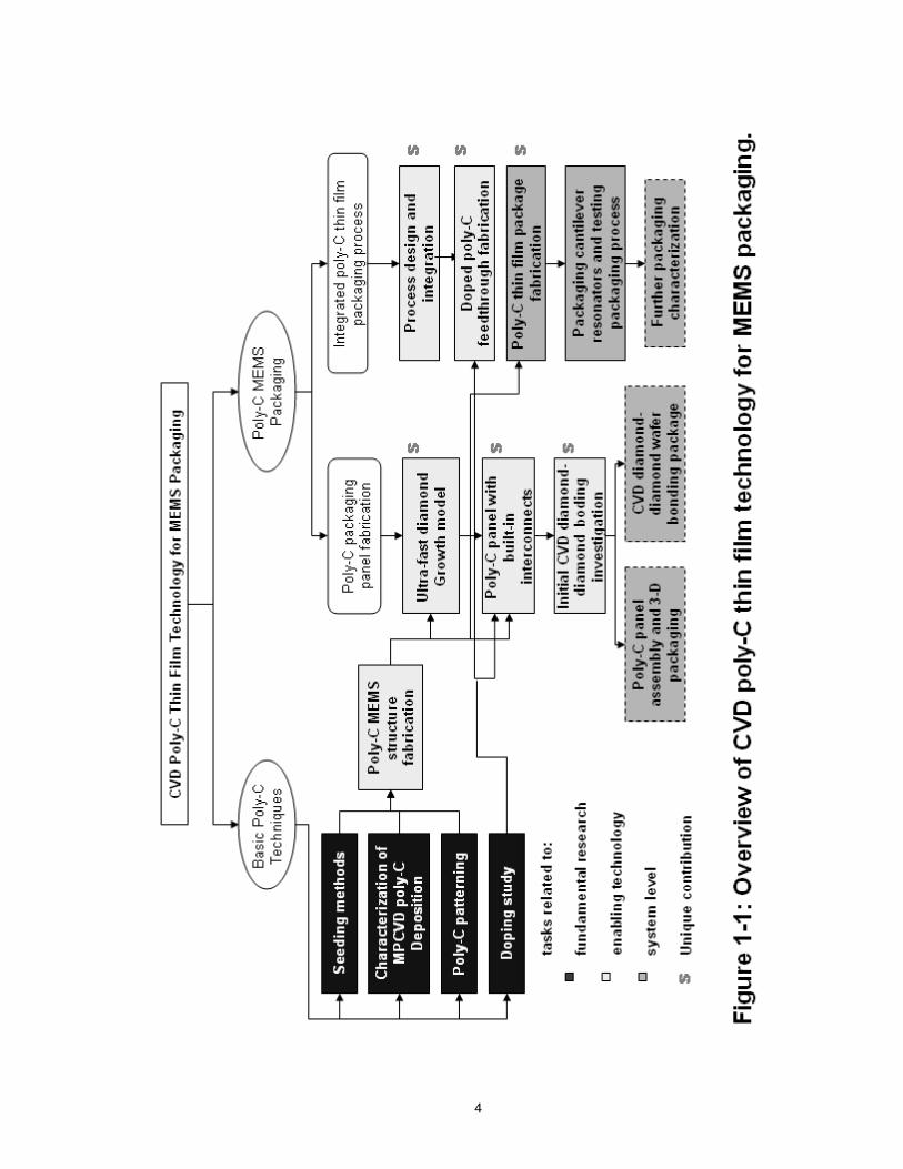
4
5
fundamental research of characterization and improvement of basic poly-C
techniques, such as diamond seeding methods, microwave plasma CVD poly-C
growth and doping technology. Then several enabling technologies have been
developed for both research directions. However, this dissertation will have an
emphasis on the poly-C thin film encapsulation packaging process, including
process design, test package fabrication and evaluation. This work involves
following specific goals:
• Low temperature poly-C deposition and characterization;
• Develop and improve different seeding methods for different substrate
surfaces;
• Free-standing poly-C micro structures fabrication;
• Ultra-fast diamond growth model;
• Resistivity study of in-situ doped poly-C film;
• Develop a package panel with built-in electrical interconnection;
• Diamond-diamond CVD bonding technology;
• Integrated post-MEMS poly-C thin film package design, fabrication and
characterization.
1.3 Dissertation Organization
Chapter 2 presents an overview of the current MEMS packaging
technologies, diamond properties and its applications in MEMS. In chapter 3,
6
fundamental poly-C technologies used in this study are outlined. The detail
description of the film deposition system, MPCVD, is given. Seeding, deposition,
doping, patterning and characterization of diamond film are investigated. Chapter
4 focuses on the fabrication technology for packaging panel applications,
including the ultra-fast growth model, packaging panel with built-in interconnects
and initial diamond-diamond bonding investigation. Chapter 5 presents the
details of the design, fabrication and evaluation of poly-C thin film encapsulation
packaging process. To evaluate the efficacy of poly-C encapsulation, poly-C
cantilever beam resonators were tested using piezoelectric actuation and laser
detection method before and after poly-C packaging process. Chapter 6 presents
conclusions of this study and considers possible future directions.
7
Chapter 2
Background
2.1 Introduction
This chapter presents an overview of the current MEMS packaging
technologies. After reviewing general MEMS packaging issues, various MEMS
packaging approaches are summarized. Diamond properties are briefly
discussed. Chemical Vapor Deposition (CVD) polycrystalline diamond (poly-C)
growth mechanism is discussed and difference CVD deposition techniques are
compared. Finally, some of the current applications of poly-C on MEMS are
reviewed.
2.2 MEMS Packaging Overview
MEMS packaging is a major challenge to Microsystems industries.
Although MEMS fabrication uses process and tools borrowed from
microelectronic industries with modification, MEMS design is quite different from
its microelectronic counterpart. In microelectronics, chip design and fabrication
process is highly industrialized and standardized, leading to possible
development of packaging standards. As long as the package can protect the
chip from outside influences and provide electrical interconnection and heat flow
path for power dissipation, a single package type can be used for different kinds
8
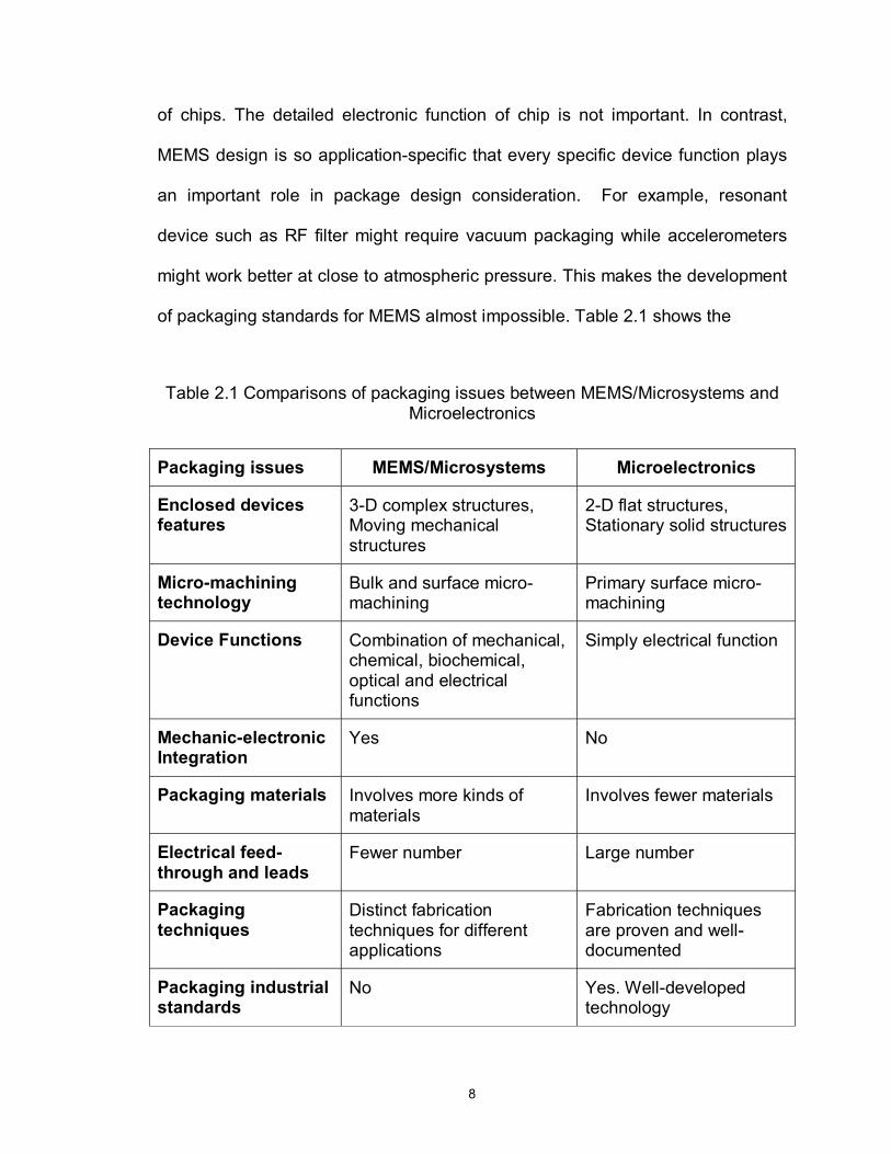
of chips. The detailed electronic function of chip is not important. In contrast,
MEMS design is so application-specific that every specific device function plays
an important role in package design consideration. For example, resonant
device such as RF filter might require vacuum packaging while accelerometers
might work better at close to atmospheric pressure. This makes the development
of packaging standards for MEMS almost impossible. Table 2.1 shows the
Table 2.1 Comparisons of packaging issues between MEMS/Microsystems and
Microelectronics
Packaging issues MEMS/Microsystems Microelectronics
Enclosed devices features
3-D complex structures, Moving mechanical structures
2-D flat structures, Stationary solid structures
Micro-machining technology
Bulk and surface micro-machining
Primary surface micro-machining
Device Functions Combination of mechanical, chemical, biochemical, optical and electrical functions
Simply electrical function
Mechanic-electronic Integration
Yes No
Packaging materials Involves more kinds of materials
Involves fewer materials
Electrical feed-through and leads
Fewer number Large number
Packaging techniques
Distinct fabrication techniques for different applications
Fabrication techniques are proven and well-documented
Packaging industrial standards
No Yes. Well-developed technology
9
comparison of packaging issues for MEMS and microelectronics. Therefore,
packaging and package design must be closely coupled with system and device
design. The packaging process must be integrated into entire
MEMS/Microsystems’s fabrication process. Furthermore, the application-oriented
packaging design tends to increase the cost of the package relative to the device.
The packaging cost of MEMS/Microsystems may vary from a moderate 20% for a
simple plastic encapsulated pressure sensors to a high 95% for a special
pressure sensor that are expected to sustain at extremely high pressure with
steep temperature rise [19].
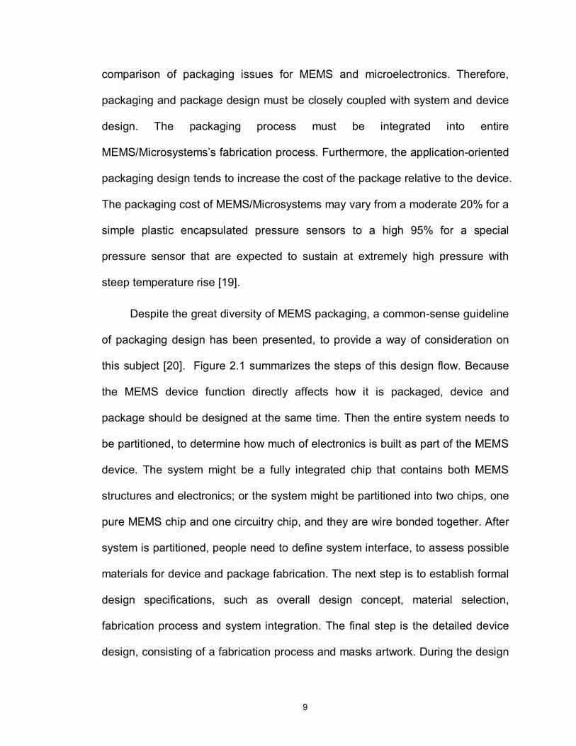
Despite the great diversity of MEMS packaging, a common-sense guideline
of packaging design has been presented, to provide a way of consideration on
this subject [20]. Figure 2.1 summarizes the steps of this design flow. Because
the MEMS device function directly affects how it is packaged, device and
package should be designed at the same time. Then the entire system needs to
be partitioned, to determine how much of electronics is built as part of the MEMS
device. The system might be a fully integrated chip that contains both MEMS
structures and electronics; or the system might be partitioned into two chips, one
pure MEMS chip and one circuitry chip, and they are wire bonded together. After
system is partitioned, people need to define system interface, to assess possible
materials for device and package fabrication. The next step is to establish formal
design specifications, such as overall design concept, material selection,
fabrication process and system integration. The final step is the detailed device
design, consisting of a fabrication process and masks artwork. During the design
10
procedure, early results either guide the way to improvement of the design, or
may force a major modification in device or package concept. Therefore, each
step in this design flow will be visited iteratively until the design converges.
MEMS packages are expected to provide MEMS devices and on-chip
circuits with functions such as mechanical support, protection from environment,
electrical interconnection and thermal management. First of all, due to the very
nature of MEMS being mechanical, it is easy to understand the importance of the
mechanical support and protection of the device from thermal and mechanical
shock, vibration, high acceleration, and other physical damage during storage
and operation. The mechanical stress endured depends on the mission or
Device AND Package Design
System Partitioning
Define Interfaces
Design Specifications
Detailed Design
Figure 2.1 Schematic flow-chart for MEMS device and package design.
11
application. If the materials are unmatched or if the silicon is subject to tensile
stress, thermal shock or thermal cycling may cause die cracking. The coefficient
of thermal expansion (CTE) of the package materials should be equal to or
slightly greater than the CTE of silicon for reliability. Secondly, in addition to the
simple protection from physical damages, MEMS packages tend to be hermetic
to protect encapsulated device from any harsh environmental influences.
Therefore, package materials should be good barriers to liquids and gases, and
have good corrosion-resistance. MEMS packages also provide interface between
microstructures and other system components. The higher of system integration
level, the more concerns of number of electrical interconnects and material they
are made of. Meanwhile, highly integration system brings another issue into
design consideration: thermal management of power dissipation.
Closely tied with the IC silicon-processing technology, which is widely used
currently, MEMS packaging can take advantage of these mature chip-scale
packaging techniques, including flip-chip and ball-grid-array techniques [1-3].
However, due to its diversity, MEMS packaging is still complicated. Recently, the
developments in MEMS area have led to growing interests in MEMS packaging
at wafer level, to reduce the packaging and testing cost. Various approaches in
this area can be characterized into two main categories: integrated encapsulation
process and wafer bonding process [4]. Integrated process adds extra steps,
such as film deposition, patterning and etching into MEMS fabrication process, to
build micro encapsulation to protect MEMS structures [21][22]. Typical examples
are an epitaxial silicon cap to seal microstructures [5] and a silicon nitride shell to
12
seal mechanical resonator for wireless communication applications [6]. Wafer
bonding process use different bonding methods like fusion bonding, anodic
bonding, eutectic bonding and solder bonding to encapsulate microstructures by
using a second substrate of silicon, glass or other materials [7][23-28].
Unfortunately, while the integrated processes suffer from the drawbacks of
process-dependency, the wafer bonding process suffers from the requirement of
high temperature and flat surface of bonding. Therefore, it is really difficult to
establish a universal process of MEMS packaging at wafer level. However, there
is a tremendous need for a versatile MEMS packaging process at the wafer-level
after devices are completed. There are great efforts have been conducted in this
direction and an unique approach of MEMS packaging by localized heating and
bonding was proposed [8].
In addition to develop and improve conventional MEMS packaging
technologies, there is also a tremendous need for exploring the applications of
new material technologies on MEMS packaging, especially for harsh
environments. Typical materials used for MEMS and its packaging are listed in
Table 2.2. In practice, there are a wide variety of materials that are involved in
MEMS and packaging, it is not possible to track all new materials developed for
MEMS and packaging recently. However, due to its extreme hardness, chemical
and mechanical stability, large band gap and highest thermal conductivity,
chemical vapor deposited (CVD) polycrystalline diamond (poly-C) has emerged
as a novel material for MEMS applications, on both micro device and packaging.
13
Table 2.2 Typical Materials used in MEMS
Semiconductors Silicon, poly-Si, GaAs
Insulators Silicon Nitride (Si3N4), Silicon Oxide (SiO2), Alumina (Al2O3)
Metals Aluminum, Gold, Titanium, Copper, Chromium, Nickel, etc.
Polymers Polyimide, Parylene, Plastic
Others Ceramic, poly-diamond
2.3 MEMS Packaging Approaches
Although MEMS packaging is very application-specific and no universal
packaging process has been established yet, various MEMS packaging
approaches at wafer level can be characterized into two main categories: wafer
boding process and integrated encapsulation process. No matter which kind of
process is used to package freestanding MEMS structure, the packaging process
should be considered from the beginning of the system development and it
should be integrated into device fabrication process. The integration of MEMS
device and related circuit chips into a system also requires multi-chip packaging
and 3D packaging technologies. In following sections, these three kinds of
approaches, with specific examples, will be discussed.
2.3.1 Wafer-bonding packaging process
14
Wafer bonding process uses different bonding methods like anodic bonding,
fusion bonding, and eutectic bonding to encapsulate microstructures by using a
second substrate of silicon, glass or other materials. This is a technology that has
found widespread use in IC as well as MEMS fabrication. Applications include
packaging, fabrication of 3-D structure and multi-layer device. As for packaging,
this process is about to bond the surfaces of wafers, to serves as a hermetic seal
of micro-device. This process can bring the MEMS packaging to wafer-level.
There are two principal requirements for achieving good surface bonding: (1)
intimate surface contact, and (2) bonding temperature. While “intimate surface
contact” requires flat and clean contact surface, and certain contact pressure to
ensure the quality of bonding, “bonding temperature” provides the required
energy for the bonding.
Following sections present the typical wafer bonding techniques and
related applications.
2.3.1.1 Anodic bonding
Anodic bonding technique is also called electrostatic bonding, since it
applies high electrostatic DC voltage to generate large electrostatic force, pulling
two wafers together. This bonding technique is widely used in MEMS packaging
due to the relatively simple set-up and low cost. Another advantage of this
bonding technique is that the bonding temperature is in the range of 200 to 450
LC, which provide better process temperature compatibility and results in low
residual stress after the bonding.
15
Typical applications of anodic bonding include silicon-glass, silicon-silicon
and glass-glass bonding. Among these applications, silicon-glass bonding is the
most common one. Typically, Pyrex 7740 glass is used in this bonding process
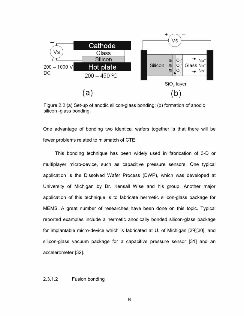
because it is rich in Sodium and has close CTE to silicon. Figure 2.2 (a) shows
the set-up for silicon-glass anodic bonding. A DC voltage in the range of 200 –
1000 V is applied and wafers are heated to a temperature about 400 LC. The
bonding of silicon and glass is accomplished by the formation of a thin layer of
SiO2 interface, as shown in Figure 2.2 (b). The presence of electrical field attracts
sodium ions (Na+) in the glass towards the cathode, leaving a Na+ depletion area
with oxygen ions (O2-). These oxygen ions react with contacting silicon to form a
SiO2 interface layer (equation 1), serving as the bond between silicon wafer and
glass wafer. To accomplish successful anodic bonding, both silicon and glass
wafers usually are double-sided polished and wafer surfaces are cleaned to be
particulates-free.
Si + 2O2- = SiO2 + 4e- (2.1)
Anodic bonding can also be used to bond two silicon wafers or two glass
wafers together. However, the process is not as straightforward as silicon-glass
bonding. Since the migration of sodium ions (Na+) and oxygen ions (O2-) are the
principal factors for anodic bonding, certain treatment should be applied on the
bonding surface of the wafers. While a thin layer of glass that is in rich of sodium
and oxygen ions is used as the intermediate layer for silicon-silicon bonding, a
thin layer of SiO2 will serve as the intermediate layer for glass-glass bonding.
16
One advantage of bonding two identical wafers together is that there will be
fewer problems related to mismatch of CTE.
This bonding technique has been widely used in fabrication of 3-D or
multiplayer micro-device, such as capacitive pressure sensors. One typical
application is the Dissolved Wafer Process (DWP), which was developed at
University of Michigan by Dr. Kensall Wise and his group. Another major
application of this technique is to fabricate hermetic silicon-glass package for
MEMS. A great number of researches have been done on this topic. Typical
reported examples include a hermetic anodically bonded silicon-glass package
for implantable micro-device which is fabricated at U. of Michigan [29][30], and
silicon-glass vacuum package for a capacitive pressure sensor [31] and an
accelerometer [32].
2.3.1.2 Fusion bonding
Figure 2.2 (a) Set-up of anodic silicon-glass bonding; (b) formation of anodic silicon -glass bonding.
17
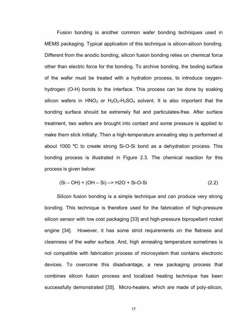
Fusion bonding is another common wafer bonding techniques used in
MEMS packaging. Typical application of this technique is silicon-silicon bonding.
Different from the anodic bonding, silicon fusion bonding relies on chemical force
other than electric force for the bonding. To archive bonding, the boding surface
of the wafer must be treated with a hydration process, to introduce oxygen-
hydrogen (O-H) bonds to the interface. This process can be done by soaking
silicon wafers in HNO3 or H2O2-H2SO4 solvent. It is also important that the
bonding surface should be extremely flat and particulates-free. After surface
treatment, two wafers are brought into contact and some pressure is applied to
make them stick initially. Then a high-temperature annealing step is performed at
about 1000 LC to create strong Si-O-Si bond as a dehydration process. This
bonding process is illustrated in Figure 2.3. The chemical reaction for this
process is given below:
(Si – OH) + (OH – Si) --> H2O + Si-O-Si (2.2)
Silicon fusion bonding is a simple technique and can produce very strong
bonding. This technique is therefore used for the fabrication of high-pressure
silicon sensor with low cost packaging [33] and high-pressure bipropellant rocket
engine [34]. However, it has some strict requirements on the flatness and
cleanness of the wafer surface. And, high annealing temperature sometimes is
not compatible with fabrication process of microsystem that contains electronic
devices. To overcome this disadvantage, a new packaging process that
combines silicon fusion process and localized heating technique has been
successfully demonstrated [35]. Micro-heaters, which are made of poly-silicon,
18
are patterned in confined bonding region, to provide localized high temperature
heating for fusion bonding. Without regular global heating, the substrate
temperature remains low.
2.3.1.3 Eutectic bonding
Eutectic bonding involves the diffusion of atoms of eutectic alloys into the
atomic structures of the wafers to be bonded together, thus forms solid bonding
of these wafers. To accomplish this bonding, one must first select a candidate
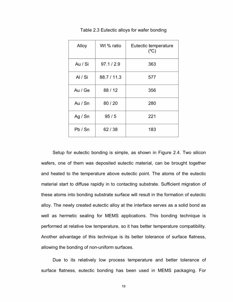
material that will form a eutectic alloy with the materials to be bonded. Table 2.3
provides a list of eutectic alloys with their eutectic temperatures. The most
commonly used material to form a eutectic bonding with silicon is gold (Au) or
alloys that composes gold.
Figure 2.3 Silicon fusion bonding set-up
19
Table 2.3 Eutectic alloys for wafer bonding
Alloy Wt % ratio Eutectic temperature (LC)
Au / Si 97.1 / 2.9 363
Al / Si 88.7 / 11.3 577
Au / Ge 88 / 12 356
Au / Sn 80 / 20 280
Ag / Sn 95 / 5 221
Pb / Sn 62 / 38 183
Setup for eutectic bonding is simple, as shown in Figure 2.4. Two silicon
wafers, one of them was deposited eutectic material, can be brought together
and heated to the temperature above eutectic point. The atoms of the eutectic
material start to diffuse rapidly in to contacting substrate. Sufficient migration of
these atoms into bonding substrate surface will result in the formation of eutectic
alloy. The newly created eutectic alloy at the interface serves as a solid bond as
well as hermetic sealing for MEMS applications. This bonding technique is
performed at relative low temperature, so it has better temperature compatibility.
Another advantage of this technique is its better tolerance of surface flatness,
allowing the bonding of non-uniform surfaces.
Due to its relatively low process temperature and better tolerance of
surface flatness, eutectic bonding has been used in MEMS packaging. For
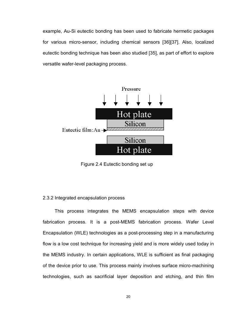
20
example, Au-Si eutectic bonding has been used to fabricate hermetic packages
for various micro-sensor, including chemical sensors [36][37]. Also, localized
eutectic bonding technique has been also studied [35], as part of effort to explore
versatile wafer-level packaging process.
2.3.2 Integrated encapsulation process
This process integrates the MEMS encapsulation steps with device
fabrication process. It is a post-MEMS fabrication process. Wafer Level
Encapsulation (WLE) technologies as a post-processing step in a manufacturing
flow is a low cost technique for increasing yield and is more widely used today in
the MEMS industry. In certain applications, WLE is sufficient as final packaging
of the device prior to use. This process mainly involves surface micro-machining
technologies, such as sacrificial layer deposition and etching, and thin film
Figure 2.4 Eutectic bonding set up
21
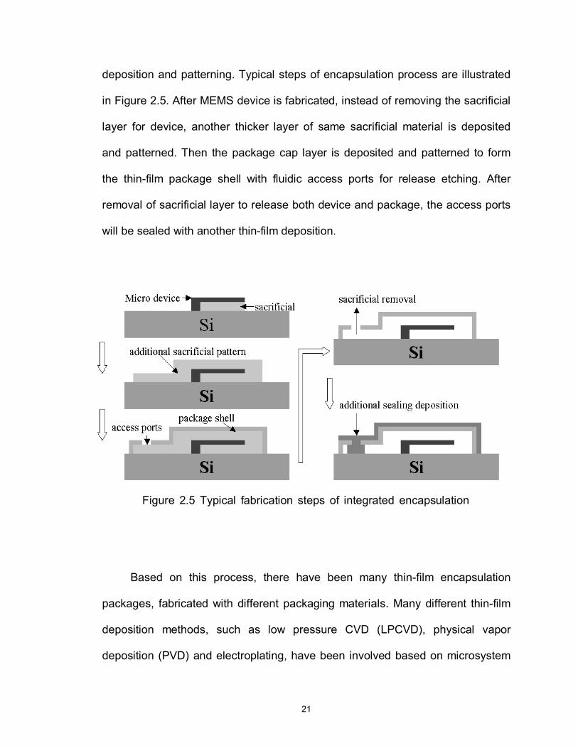
deposition and patterning. Typical steps of encapsulation process are illustrated
in Figure 2.5. After MEMS device is fabricated, instead of removing the sacrificial
layer for device, another thicker layer of same sacrificial material is deposited
and patterned. Then the package cap layer is deposited and patterned to form
the thin-film package shell with fluidic access ports for release etching. After
removal of sacrificial layer to release both device and package, the access ports
will be sealed with another thin-film deposition.
Based on this process, there have been many thin-film encapsulation
packages, fabricated with different packaging materials. Many different thin-film
deposition methods, such as low pressure CVD (LPCVD), physical vapor
deposition (PVD) and electroplating, have been involved based on microsystem
Figure 2.5 Typical fabrication steps of integrated encapsulation
22
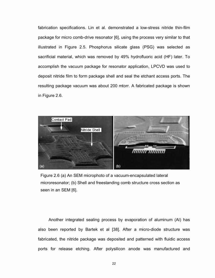
fabrication specifications. Lin et al. demonstrated a low-stress nitride thin-film
package for micro comb-drive resonator [6], using the process very similar to that
illustrated in Figure 2.5. Phosphorus silicate glass (PSG) was selected as
sacrificial material, which was removed by 49% hydrofluoric acid (HF) later. To
accomplish the vacuum package for resonator application, LPCVD was used to
deposit nitride film to form package shell and seal the etchant access ports. The
resulting package vacuum was about 200 mtorr. A fabricated package is shown
in Figure 2.6.
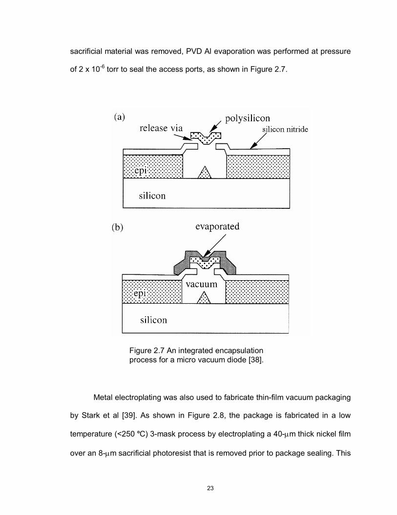
Another integrated sealing process by evaporation of aluminum (Al) has
also been reported by Bartek et al [38]. After a micro-diode structure was
fabricated, the nitride package was deposited and patterned with fluidic access
ports for release etching. After polysilicon anode was manufactured and
Figure 2.6 (a) An SEM microphoto of a vacuum-encapsulated lateral
microresonator; (b) Shell and freestanding comb structure cross section as
seen in an SEM [6].
23
sacrificial material was removed, PVD Al evaporation was performed at pressure
of 2 x 10⁻⁶ torr to seal the access ports, as shown in Figure 2.7.
Metal electroplating was also used to fabricate thin-film vacuum packaging
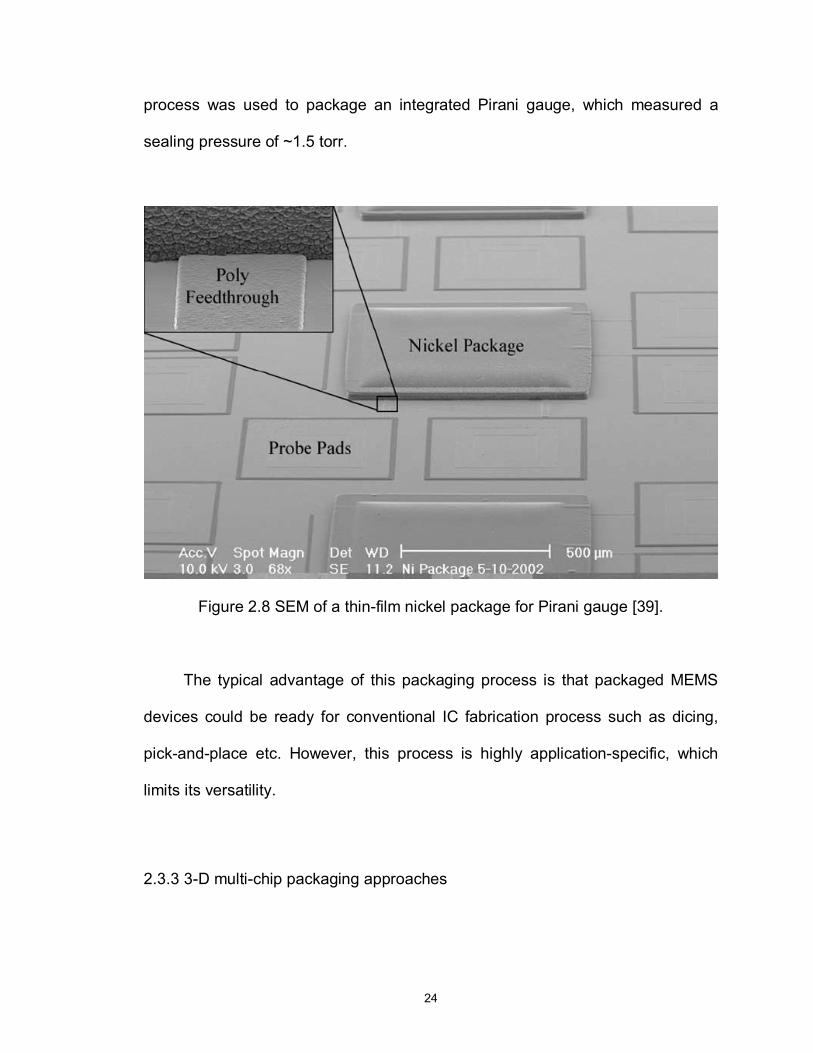
by Stark et al [39]. As shown in Figure 2.8, the package is fabricated in a low
temperature (<250 LC) 3-mask process by electroplating a 40-µm thick nickel film
over an 8-µm sacrificial photoresist that is removed prior to package sealing. This
Figure 2.7 An integrated encapsulation process for a micro vacuum diode [38].
24
process was used to package an integrated Pirani gauge, which measured a
sealing pressure of ~1.5 torr.
Figure 2.8 SEM of a thin-film nickel package for Pirani gauge [39].
The typical advantage of this packaging process is that packaged MEMS
devices could be ready for conventional IC fabrication process such as dicing,
pick-and-place etc. However, this process is highly application-specific, which
limits its versatility.
2.3.3 3-D multi-chip packaging approaches
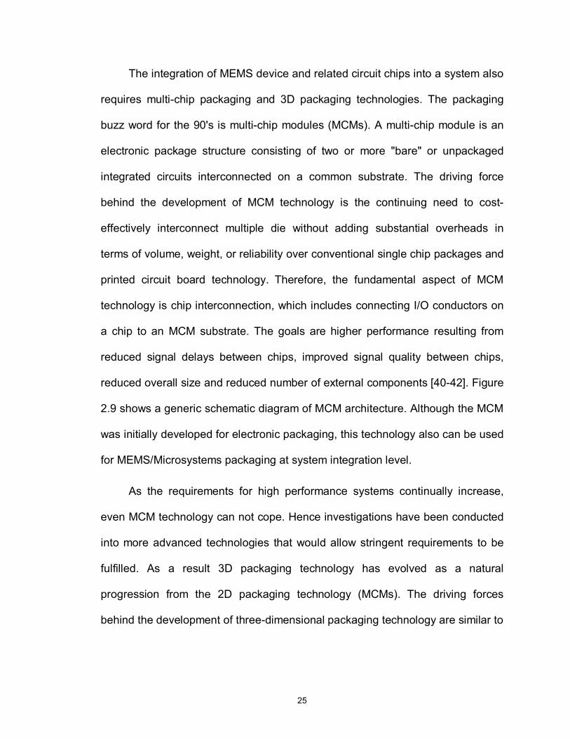
25
The integration of MEMS device and related circuit chips into a system also
requires multi-chip packaging and 3D packaging technologies. The packaging
buzz word for the 90's is multi-chip modules (MCMs). A multi-chip module is an
electronic package structure consisting of two or more "bare" or unpackaged
integrated circuits interconnected on a common substrate. The driving force
behind the development of MCM technology is the continuing need to cost-
effectively interconnect multiple die without adding substantial overheads in
terms of volume, weight, or reliability over conventional single chip packages and
printed circuit board technology. Therefore, the fundamental aspect of MCM
technology is chip interconnection, which includes connecting I/O conductors on
a chip to an MCM substrate. The goals are higher performance resulting from
reduced signal delays between chips, improved signal quality between chips,
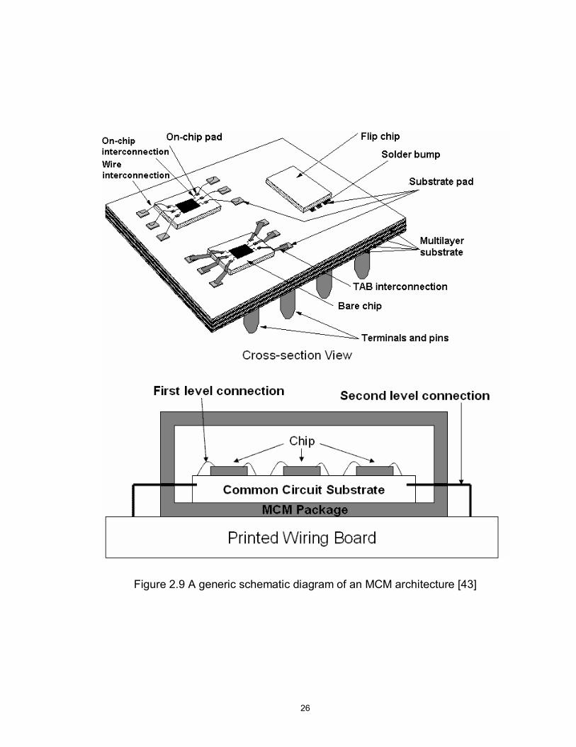
reduced overall size and reduced number of external components [40-42]. Figure
2.9 shows a generic schematic diagram of MCM architecture. Although the MCM
was initially developed for electronic packaging, this technology also can be used
for MEMS/Microsystems packaging at system integration level.
As the requirements for high performance systems continually increase,
even MCM technology can not cope. Hence investigations have been conducted
into more advanced technologies that would allow stringent requirements to be
fulfilled. As a result 3D packaging technology has evolved as a natural
progression from the 2D packaging technology (MCMs). The driving forces
behind the development of three-dimensional packaging technology are similar to
26
Figure 2.9 A generic schematic diagram of an MCM architecture [43]
27
the MCM technology, although the requirements for the 3D technology are more
aggressive. These requirements include the need for significant size and weight
reductions, higher performance, small delay, higher reliability and, potentially,
reduced power consumption. Several different multi-chip module technologies
have been studied, including chip scale packaging using solder, wire bonding,
flex substrates, epoxy layers, filled vias, micro-relays, and ceramic clusters for
manufacturing dense packages [43-46].
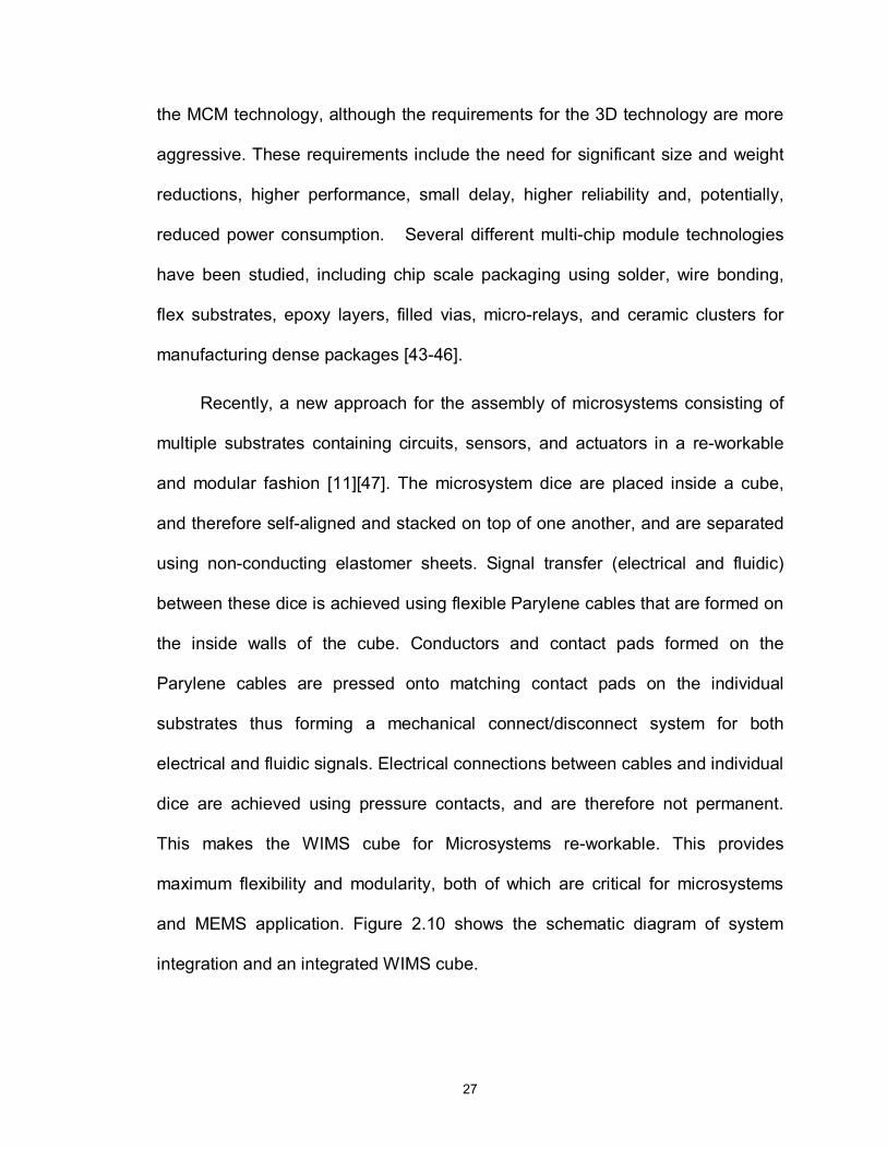
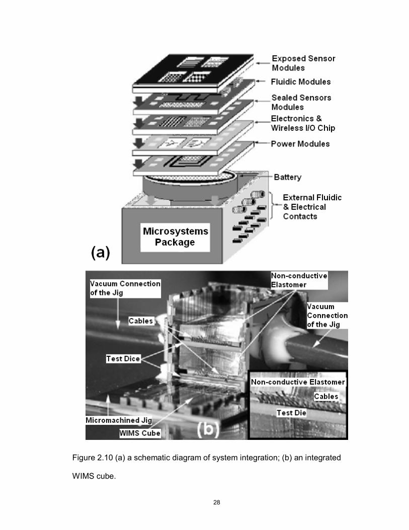
Recently, a new approach for the assembly of microsystems consisting of
multiple substrates containing circuits, sensors, and actuators in a re-workable
and modular fashion [11][47]. The microsystem dice are placed inside a cube,
and therefore self-aligned and stacked on top of one another, and are separated
using non-conducting elastomer sheets. Signal transfer (electrical and fluidic)
between these dice is achieved using flexible Parylene cables that are formed on
the inside walls of the cube. Conductors and contact pads formed on the
Parylene cables are pressed onto matching contact pads on the individual
substrates thus forming a mechanical connect/disconnect system for both
electrical and fluidic signals. Electrical connections between cables and individual
dice are achieved using pressure contacts, and are therefore not permanent.
This makes the WIMS cube for Microsystems re-workable. This provides
maximum flexibility and modularity, both of which are critical for microsystems
and MEMS application. Figure 2.10 shows the schematic diagram of system
integration and an integrated WIMS cube.
28
Figure 2.10 (a) a schematic diagram of system integration; (b) an integrated
WIMS cube.
29
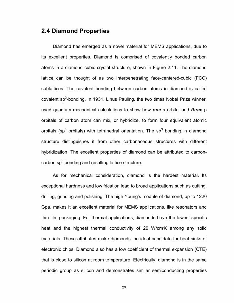
2.4 Diamond Properties
Diamond has emerged as a novel material for MEMS applications, due to
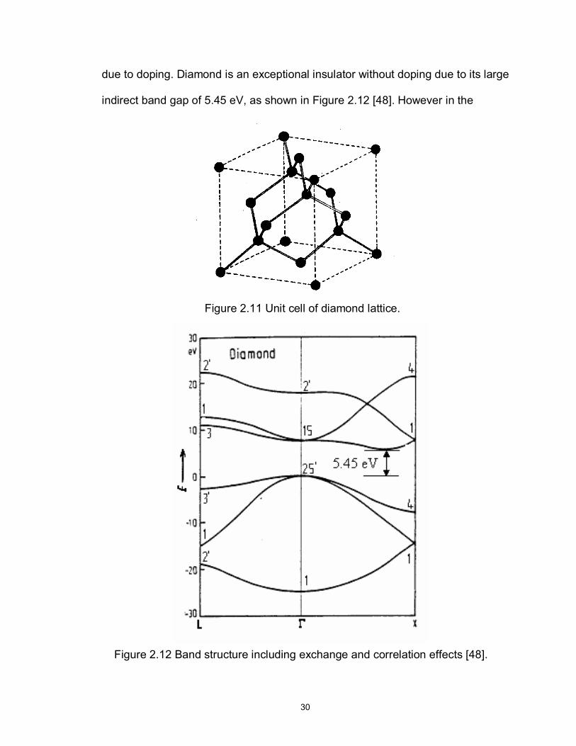
its excellent properties. Diamond is comprised of covalently bonded carbon
atoms in a diamond cubic crystal structure, shown in Figure 2.11. The diamond
lattice can be thought of as two interpenetrating face-centered-cubic (FCC)
sublattices. The covalent bonding between carbon atoms in diamond is called
covalent sp3-bonding. In 1931, Linus Pauling, the two times Nobel Prize winner,
used quantum mechanical calculations to show how one s orbital and three p
orbitals of carbon atom can mix, or hybridize, to form four equivalent atomic
orbitals (sp3 orbitals) with tetrahedral orientation. The sp3 bonding in diamond
structure distinguishes it from other carbonaceous structures with different
hybridization. The excellent properties of diamond can be attributed to carbon-
carbon sp3 bonding and resulting lattice structure.
As for mechanical consideration, diamond is the hardest material. Its
exceptional hardness and low frication lead to broad applications such as cutting,
drilling, grinding and polishing. The high Young’s module of diamond, up to 1220
Gpa, makes it an excellent material for MEMS applications, like resonators and
thin film packaging. For thermal applications, diamonds have the lowest specific
heat and the highest thermal conductivity of 20 W/cm.K among any solid
materials. These attributes make diamonds the ideal candidate for heat sinks of
electronic chips. Diamond also has a low coefficient of thermal expansion (CTE)
that is close to silicon at room temperature. Electrically, diamond is in the same
periodic group as silicon and demonstrates similar semiconducting properties
30
due to doping. Diamond is an exceptional insulator without doping due to its large
indirect band gap of 5.45 eV, as shown in Figure 2.12 [48]. However in the
Figure 2.11 Unit cell of diamond lattice.
Figure 2.12 Band structure including exchange and correlation effects [48].
31
presence of trace amounts of boron, the substance becomes a semiconductor.
Diamond's excellent thermal characteristics also make it an ideal semiconductor,
since it will be much more resistant to heat than silicon. Optically, diamonds are
special, giving it its distinctive place in jewellery. Its high refractive index (2.41)
provides it with a steep angle (24 degrees off normal) for total internal reflection.
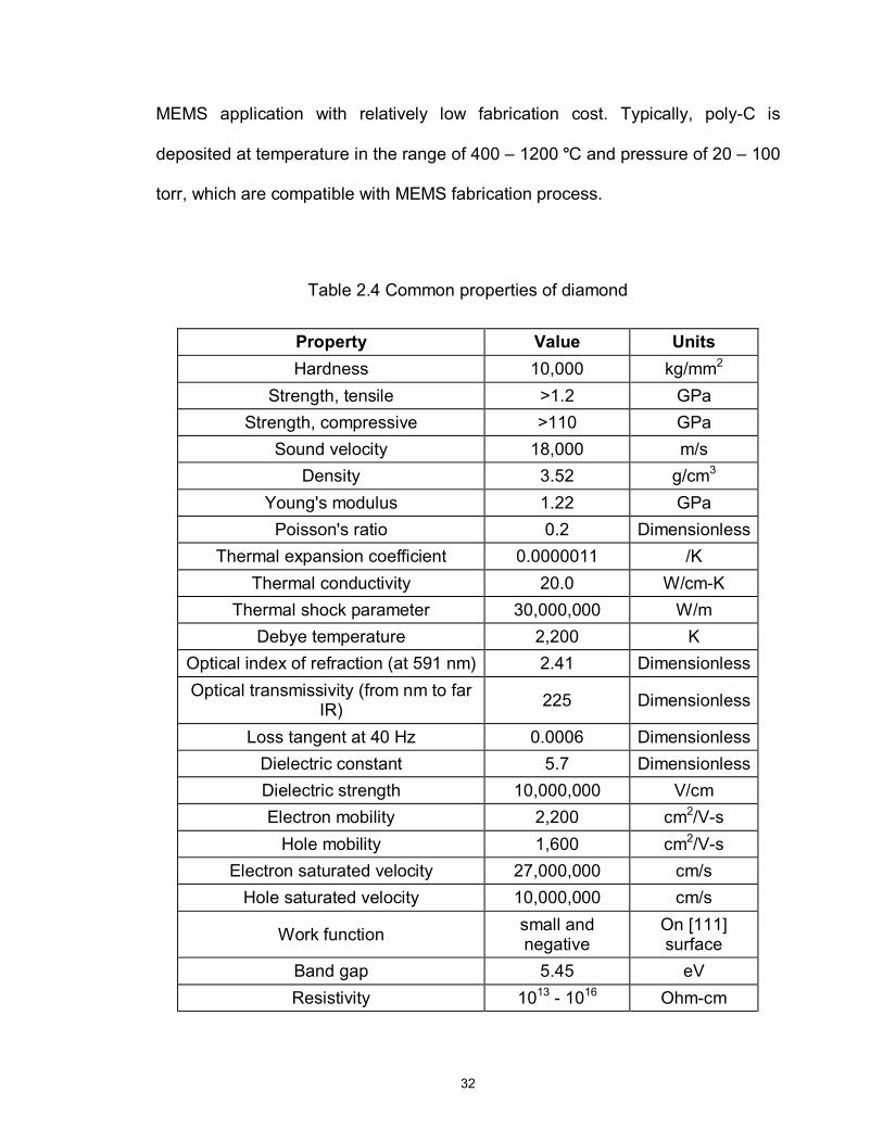
The properties of diamond are summarized in Table 2.4 [49].
There are several types of diamonds for different applications, including
nature diamonds, synthetic industrial diamonds and CVD polycrystalline
diamonds. Natural diamonds are classified by the type of Ia, Ib, IIa and IIb, based
on the quantity of impurities (Nitrogen) found within them. Type Ia is the most
common type of natural diamond, containing up to 0.3% nitrogen. All other three
types are very few in nature. Synthetic industrial diamonds are produced by High
Pressure High Temperature (HPHT) Synthesis process. In HPHT synthesis,
graphite and a metallic catalyst are placed in a hydraulic press under high
temperatures and pressures. Over the period of a few hours the graphite
converts to diamond. The resulting diamonds are usually a few millimeters in size
and too flawed for use as gemstones, but they are extremely useful as edges on
cutting tools and drill-bits and for being compressed to generate very high
pressures. Nearly all-synthetic industrial diamonds are type Ib, containing up to 5
ppm nitrogen. Both nature diamond and synthetic diamond are single-crystalline.
Considering the high cost, HPHT synthetic condition and difficulty of processing,
these two types of diamonds are very limited in MEMS applications. Instead,
CVD poly-crystalline diamond (poly-C) can provides still remarkable quality for
32
MEMS application with relatively low fabrication cost. Typically, poly-C is
deposited at temperature in the range of 400 – 1200 LC and pressure of 20 – 100
torr, which are compatible with MEMS fabrication process.
Table 2.4 Common properties of diamond
Property Value Units Hardness 10,000 kg/mm2
Strength, tensile >1.2 GPa Strength, compressive >110 GPa
Sound velocity 18,000 m/s Density 3.52 g/cm3
Young's modulus 1.22 GPa Poisson's ratio 0.2 Dimensionless
Thermal expansion coefficient 0.0000011 /K Thermal conductivity 20.0 W/cm-K
Thermal shock parameter 30,000,000 W/m Debye temperature 2,200 K
Optical index of refraction (at 591 nm) 2.41 Dimensionless Optical transmissivity (from nm to far
IR) 225 Dimensionless
Loss tangent at 40 Hz 0.0006 Dimensionless Dielectric constant 5.7 Dimensionless Dielectric strength 10,000,000 V/cm Electron mobility 2,200 cm2/V-s
Hole mobility 1,600 cm2/V-s Electron saturated velocity 27,000,000 cm/s
Hole saturated velocity 10,000,000 cm/s
Work function small and negative
On [111] surface
Band gap 5.45 eV Resistivity 1013 - 1016 Ohm-cm
33
2.5 CVD Poly-C Deposition Techniques
First evidence of diamond growth by CVD by Eversole in 1952-53 led to the
use of H2 and CH4 in the hot filament CVD (HFCVD) to grow diamond on
diamond substrates (homoepitaxial growth) by Angus in 1971. The inexpensive
CVD polycrystalline diamond (poly-C) was grown on non-diamond substrates by
Deryagin in 1976, Spitsyn in 1981, and by Matsumoto et al. in 1983.
2.5.1 CVD poly-C growth mechanism [50]
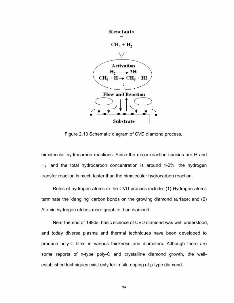
In diamond CVD processes, reaction gaseous species (CH4 + H2) are
activated into CH3 and hydrogen atom, and deposited onto substrate surface.
Currently, it is believed that, during the diamond CVD process, the CH3 is
responsible for deposition of C as diamond and non-diamond phases. The
atomic hydrogen, present in the growth environment, removes the non-diamond
phases leaving behind the diamond phase.
A CVD diamond deposition process is shown in Figure 2.13. Typically, a
mixture of 1-2% methane in hydrogen environment at pressure around 50 torr,
flow into reactor and gaseous reactions are initiated by hot filament, plasma or
other methods. The sample substrate may be pre-seeded with diamond particles.
On its surface, adsorption, diffusion, reaction and desoroption of various species
occurs leading to the nucleation of diamond particles, removal of graphite (sp2)
carbon, and ultimately the growth of a continuous diamond film. The principle gas
phase reactions involve the rapid hydrogen transfer reaction and slower
34
bimolecular hydrocarbon reactions. Since the major reaction species are H and
H2, and the total hydrocarbon concentration is around 1-2%, the hydrogen
transfer reaction is much faster than the bimolecular hydrocarbon reaction.
Roles of hydrogen atoms in the CVD process include: (1) Hydrogen atoms
terminate the 'dangling' carbon bonds on the growing diamond surface; and (2)
Atomic hydrogen etches more graphite than diamond.
Near the end of 1990s, basic science of CVD diamond was well understood,
and today diverse plasma and thermal techniques have been developed to
produce poly-C films in various thickness and diameters. Although there are
some reports of n-type poly-C and crystalline diamond growth, the well-
established techniques exist only for in-situ doping of p-type diamond.
Figure 2.13 Schematic diagram of CVD diamond process.
35
2.5.2 CVD poly-C deposition methods
A number of diamond deposition methods are currently available for the
growth of diamond. Early approaches to forming diamond from the vapour phase
were characterized by the thermal CVD techniques, including Hot Filament CVD
[51][52] and Combustion Flame CVD [53][54]. These methods use heat energy to
break down hydrogen molecules to hydrogen atoms. Later, plasma related CVD
techniques were developed. Major methods include DC arc discharge plasma
CVD [55][56], radio frequency plasma CVD [57] and microwave plasma CVD [58-
61]. With induced power, reactant gases form plasma and hydrogen molecules
are atomized. Recently, a multiple pulsed laser process with ultra high deposition
rate is being developed [62][63]. A comparison of different kinds of CVD
techniques was shown in Table 2.5, in terms of parameters like deposition rates,
deposition area, cost, advantage and disadvantages.
As shown in Table 2.5, the deposition rate of CVD diamond shows a large
variation (0.1 – 3,600 micrometers) depending on the growth technique.
Considering the overall performance, cost and quality of deposited diamond film,
microwave plasma CVD (MPCVD) method has been widely chosen to grow CVD
diamond.
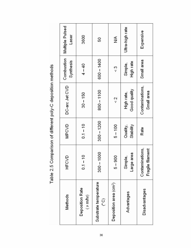
36
37
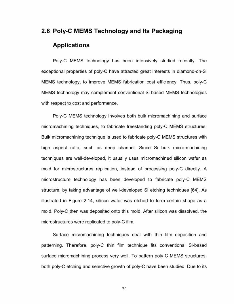
2.6 Poly-C MEMS Technology and Its Packaging
Applications
Poly-C MEMS technology has been intensively studied recently. The
exceptional properties of poly-C have attracted great interests in diamond-on-Si
MEMS technology, to improve MEMS fabrication cost efficiency. Thus, poly-C
MEMS technology may complement conventional Si-based MEMS technologies
with respect to cost and performance.
Poly-C MEMS technology involves both bulk micromachining and surface
micromachining techniques, to fabricate freestanding poly-C MEMS structures.
Bulk micromachining technique is used to fabricate poly-C MEMS structures with
high aspect ratio, such as deep channel. Since Si bulk micro-machining
techniques are well-developed, it usually uses micromachined silicon wafer as
mold for microstructures replication, instead of processing poly-C directly. A
microstructure technology has been developed to fabricate poly-C MEMS
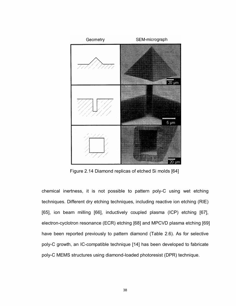
structure, by taking advantage of well-developed Si etching techniques [64]. As
illustrated in Figure 2.14, silicon wafer was etched to form certain shape as a
mold. Poly-C then was deposited onto this mold. After silicon was dissolved, the
microstructures were replicated to poly-C film.
Surface micromachining techniques deal with thin film deposition and
patterning. Therefore, poly-C thin film technique fits conventional Si-based
surface micromachining process very well. To pattern poly-C MEMS structures,
both poly-C etching and selective growth of poly-C have been studied. Due to its
38
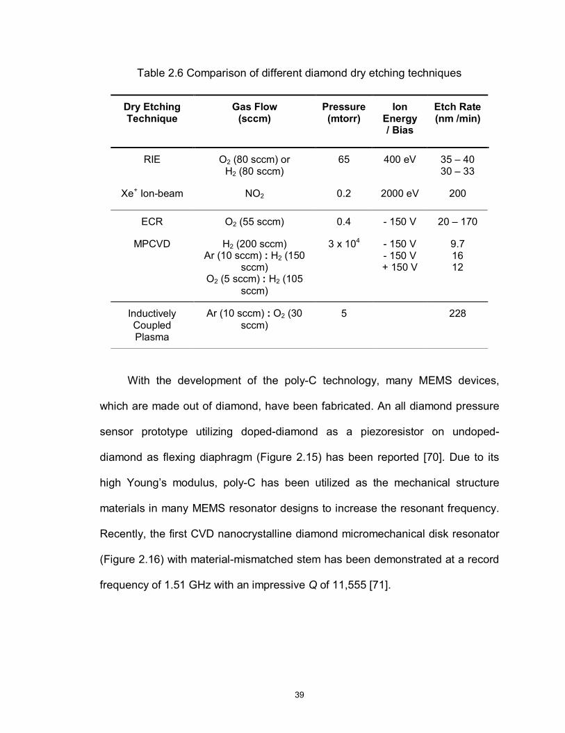
chemical inertness, it is not possible to pattern poly-C using wet etching
techniques. Different dry etching techniques, including reactive ion etching (RIE)
[65], ion beam milling [66], inductively coupled plasma (ICP) etching [67],
electron-cyclotron resonance (ECR) etching [68] and MPCVD plasma etching [69]
have been reported previously to pattern diamond (Table 2.6). As for selective
poly-C growth, an IC-compatible technique [14] has been developed to fabricate
poly-C MEMS structures using diamond-loaded photoresist (DPR) technique.
Figure 2.14 Diamond replicas of etched Si molds [64]
39
Table 2.6 Comparison of different diamond dry etching techniques
With the development of the poly-C technology, many MEMS devices,
which are made out of diamond, have been fabricated. An all diamond pressure
sensor prototype utilizing doped-diamond as a piezoresistor on undoped-
diamond as flexing diaphragm (Figure 2.15) has been reported [70]. Due to its
high Young’s modulus, poly-C has been utilized as the mechanical structure
materials in many MEMS resonator designs to increase the resonant frequency.
Recently, the first CVD nanocrystalline diamond micromechanical disk resonator
(Figure 2.16) with material-mismatched stem has been demonstrated at a record
frequency of 1.51 GHz with an impressive Q of 11,555 [71].
Dry Etching Technique
Gas Flow (sccm)
Pressure (mtorr)
Ion Energy / Bias
Etch Rate (nm /min)
RIE O2 (80 sccm) or H2 (80 sccm)
65 400 eV 35 – 40 30 – 33
Xe+ Ion-beam NO2 0.2 2000 eV 200
ECR O2 (55 sccm) 0.4 - 150 V 20 – 170
MPCVD H2 (200 sccm) Ar (10 sccm) : H2 (150
sccm) O2 (5 sccm) : H2 (105
sccm)
3 x 10⁴ - 150 V - 150 V + 150 V
9.7 16 12
Inductively Coupled Plasma
Ar (10 sccm) : O2 (30 sccm)
5 228
40
Figure 2.15 (a) SEM of etched diamond pressure sensor membrane cavity; (b) DMEMS Pressure sensor chip [44].
Figure 2.16 Fabrication process flow cross-sections and associated SEM’s at different stages of the process. (a) After diamond disk definition. (b) After polysilicon stem refilling and electrode definition [45].
Although varieties of poly-C MEMS application have been successfully
demonstrated, the typical application of diamond on MEMS packaging is still
limited to thermal management [17][72]. As mentioned before, MEMS packaging
is supposed to provide MEMS devices and on-chip circuits with functions such as
mechanical support, protection from environment, electrical interconnection as

41
well as thermal management. The exceptional properties of poly-C, other than
thermal property, should also make an impact on MEMS packaging. To explore
broader application of poly-C on MEMS packaging is the motivation of my Ph.D.
work.
42
Chapter 3
Fundamental Research on CVD Poly-C
Technology
3.1 Introduction
As mentioned in Chapter 1, the first step of this research is to perform an
intensive fundamental research on basic poly-C technologies, such as seeding
and nucleation, deposition, doping and patterning. This chapter summarizes the
characterization and optimization of these technologies. The results of this
fundamental research are used for enabling technology development and
package design and fabrication later.
3.2 Fabrication and Characterization Systems
In chapter 2, several conventional CVD diamond deposition methods are
discussed and compared. Considering the overall performance, cost and quality
of deposited diamond film, microwave plasma CVD (MPCVD) method has been
widely chosen to grow CVD diamond. To characterize deposited poly-C film,
Raman spectroscopy, scanning electron microscopy, and atomic force
microscopy have been used.
43
3.2.1 MPCVD diamond deposition system
In this study, poly-C films were synthesized using MPCVD system (Model
MPDR 313EHP, Wavemat, Inc.) with 2.45 GHz microwave generator up to 6
kilowatts. The schematic diagram is shown in Figure 3-1.
The main components of the system consist of a microwave source unit,
cylindrical microwave cavity, deposition chamber, substrate holder, Gas
distribution and pressure control unit.
The microwave source unit includes a DC power supply (Model
GMP60KSM, SairemTM), a microwave power controller (Model PIL408, SairemTM)
and a magnetron (Model GMP60KSM, SairemTM). The DC power supply drives a
magnetron source producing microwaves with frequency 2.45 GHz. The power
supply is able to deliver power between 0.6 to 6 kW. The reflected power is
absorbed by the matched load. Hence, the magnetron head is protected against
any reflected power on the transmission line.
The cylindrical microwave cavity was made of aluminum. The diameter of
the cavity was fixed at 17.78 cm and its height defined by Ls in Figure 3.1 was
changeable to tune the microwave cavity. The height of cylindrical cavity was set
to ~21.59 cm, to operate in the electromagnetic mode designated TM013 for
2.45GHz microwave. This mode was found to provide optimum film deposition
uniformity. The cylindrical quartz dome inside the microwave cavity had
dimensions of 5 inch diameter and 3.5 inch height. The microwave cavity was
essentially a termination to the microwave transmission waveguide. The
intensified microwave energy produced the plasma of the reaction gases inside
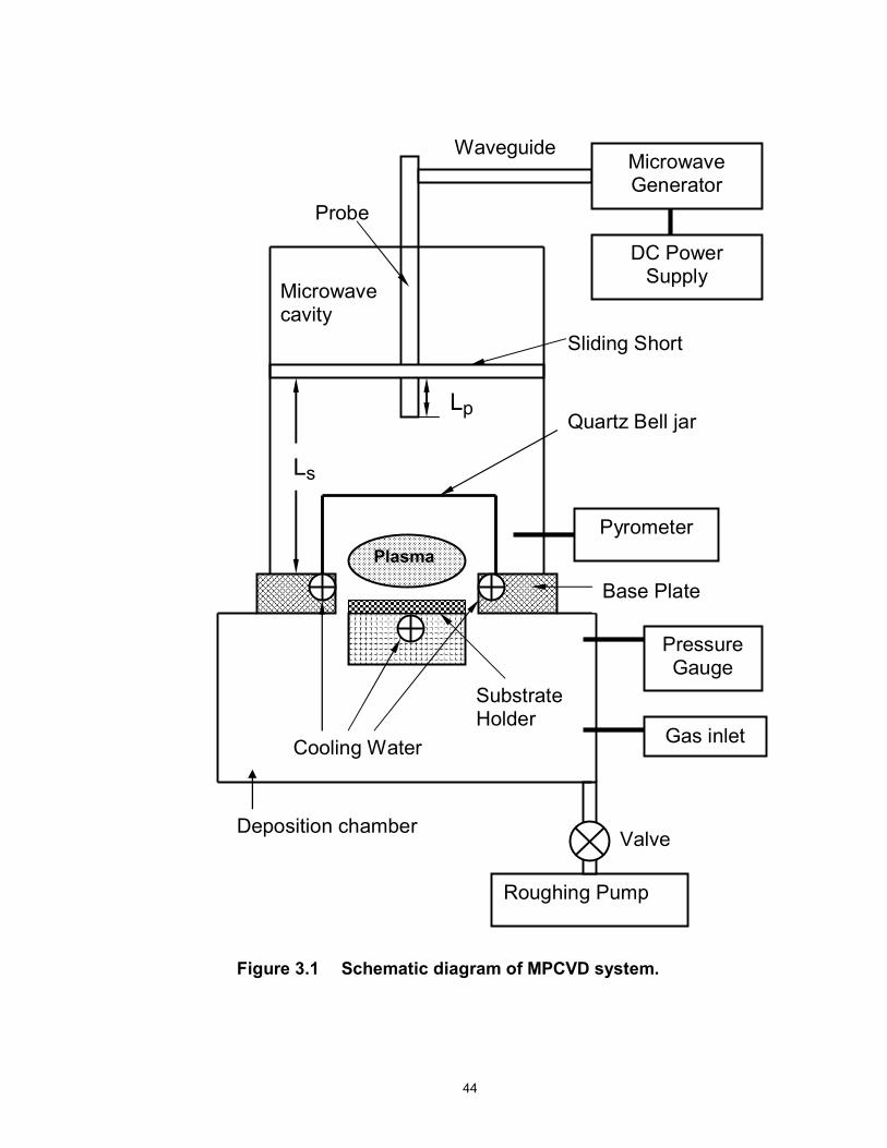
44
Quartz Bell jar
Ls
Lp
Sliding Short
Probe
Base Plate
Substrate Holder
Cooling Water
Waveguide Microwave Generator
DC Power Supply
Pressure Gauge
Gas inlet
Valve
Roughing Pump
Pyrometer
Figure 3.1 Schematic diagram of MPCVD system.
Microwave cavity
Deposition chamber
Plasma
45
quartz dome. The resonant condition of the cavity is mainly determined by the
position of the cavity short and the microwave coupling probe. The short is the
electrical top of the cavity and determines the overall length of the cavity, which
in turn controlled the operating mode of the cavity. The position of the probe,
defined by Lp in Figure 3.1, determines the electromagnetic fields near the cavity
wall and hence the coupling of the energy into the cavity. By tuning the positions
of the short and probe, the impedance of the plasma discharge/microwave cavity
is matched to that of the transmission waveguide, producing a resonant condition.
A well tuned cavity would show little or no reflected microwave power.
The deposition chamber was made of stainless steel with dimensions of
17 inch height and 18 inch diameter. The sample can be loaded and unloaded
through a 10 inch front door. The sample stage can be attached to the base plate
by sliding through two guiding rods.
Water was used to cool the cavity walls, sliding short, coupling probe, and
base plate. The jet pump (Model 9K862A, Dayton motors) was used to increase
the inlet pressure. The thermocouples (Type K, Omega Engineering, Inc.) were
used to monitor the temperature of the microwave cavity, base plate, quartz
dome, short, and probe.
Graphite or molybdenum was used as a substrate holder and
accommodates 4 inch substrate. The substrate holder had active cooling, so the
temperature of the substrate was decreasing with cooling. The substrate
temperature was observed by the infrared thermometer (Model OS3707, Omega
Engineering, Inc.).
46
The gas distribution unit consisted of four mass flow controllers (Type
1159B, MKS Instruments, Inc.) and a flow readout unit (Model 247C, MKS
Instruments, Inc.) to control the flow of the processing gases. Source gases were
mixed before reaching the inlet on the baseplate. Three capacitance manometers
(Type 622A, MKS Instruments, Inc.) were used to measure the pressure in the
chamber. The pressure controller (Type 651, MKS Instruments, Inc.) read the
pressure transducer and controls the throttle valve (Type 653, MKS Instruments,
Inc.) to achieve the desired deposition pressure. A base pressure of 10 mTorr
was achieved with the mechanical pump (Model SD-300, Varian Inc.). N2 was
used to vent the system after deposition.
3.2.2 Characterization systems
Throughout this research, the quality and properties of the poly-C films
deposited by MPCVD were characterized by tool systems such as Raman
spectroscopy, scanning electron microscopy (SEM), and atomic force
microscopy (AFM).
• Raman spectroscopy
The Raman spectroscopy is widely used in the analysis of materials, and
the identification of trace elements [73][74]. The wavenumber shift of 1332 in
Raman spectrum represents sp3 diamond peak. The Raman system (R-2001,
Ocean Optics, Inc.) consists of a diode laser, a focused probe, a CCD-array
spectrometer, an analog-to-digital converter, and operating software. The 532 nm
47
green laser with a power of 50 mW is used. The optical resolution is ~15 cm-1.
The focused probe consists of 90 µm excitation fiber and 200 µm collection fiber.
The focal length of the probe is 5 mm.
• Scanning electron microscopy (SEM)
The SEM (JEOL 6400V, Japan Electron Optics Laboratories) consists of a
LaB6 electron emitter (Noran EDS) in a vacuum chamber column and images by
collecting the secondary electrons emitted from samples due to the incident
electron beam [75]. It has a large depth of field which can be up to four hundred
times greater than that of a light microscope. It is widely utilized to inspect the
surface morphology, crystal orientation, the grain sizes, nucleation density, and
film thickness. The need for a conducting specimen somewhat limits its utility for
undoped films. The environmental SEM (ESEM) is developed to overcome the
disadvantage. ESEM maintains the sample chamber in a near-atmospheric
environment more conductive to examination of wet samples and non-conducting
samples, and has a completely different environment, high vacuum, in the
remainder of the column.
• Atomic force microscopy (AFM)
The AFM is another useful tool for studying the nucleation density, crystal
structure, and surface morphology of films. A very fine tip, mounted on a
cantilever, is scanned through the sample to obtain the surface profile. The
advantages of AFM are high resolution and great sensitivity to define profile
48
differences of vertical variations in the sample [76]. In addition, no vacuum is
needed for the operation of AFM, and it can be used on non-conducting surfaces.
3.3 Basic Poly-C Technologies
A typical CVD poly-C film fabrication involves seeding, growth, doping and
patterning. The characterization and optimization of these technologies for this
research are investigated in detail.
3.3.1 Diamond seeding technology
Diamond particle seeding is an important pre-treatment step to generate
diamond nuclei before diamond growth begins. Diamond has been shown to
nucleate on a wide variety of materials. Due to the low nucleation density on non-
diamond materials, the substrates need to be treated to enhance the nucleation
density. The commonly used pre-treatment techniques are abrading [77][78],
ultrasonic nucleation [79-81], bias enhanced nucleation (BEN) [82-84], and
electrophoresis (EP) [85-87]. Currently, three different kinds of seeding methods,
diamond-powder-loaded photoresist (DPR) [14], diamond-powder-loaded water
(DW) [88] and electrophoresis [89], are being used in the MANTL Lab at
Michigan State University.
Diamond seeding density plays an important role in the later MPCVD poly-
C deposition process. In terms of the uniformity and smoothness of poly-C films,
high seeding density usually yields better results. Different MEMS application
49
considerations, such as surface condition and substrate type, place different
process requirements on seeding method. The goal of this study is to improve
seeding density for each seeding method by optimizing the parameters of
seeding setup and operation. The characterization of different seeding methods
helps to make a right choice for application consideration.
3.3.1.1 Preparation of diamond seeds solution
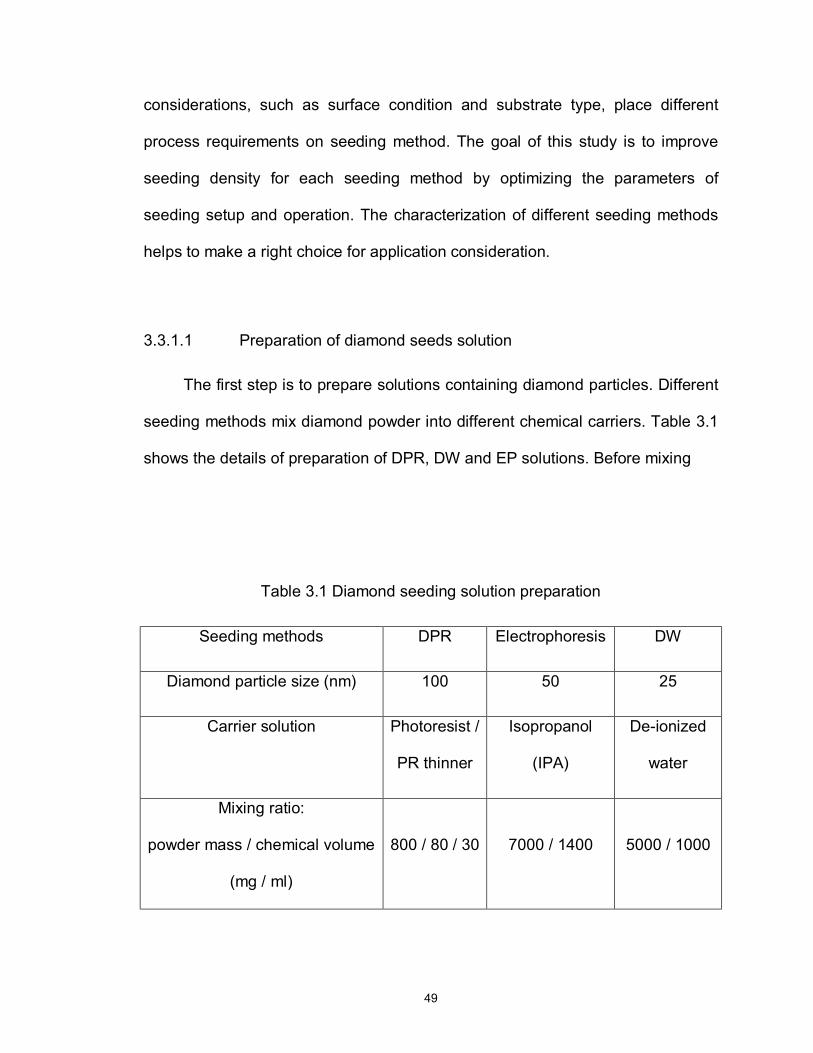
The first step is to prepare solutions containing diamond particles. Different
seeding methods mix diamond powder into different chemical carriers. Table 3.1
shows the details of preparation of DPR, DW and EP solutions. Before mixing
Table 3.1 Diamond seeding solution preparation
Seeding methods DPR Electrophoresis DW
Diamond particle size (nm) 100 50 25
Carrier solution Photoresist /
PR thinner
Isopropanol
(IPA)
De-ionized
water
Mixing ratio:
powder mass / chemical volume
(mg / ml)
800 / 80 / 30
7000 / 1400
5000 / 1000
50
diamond powder into chemicals, diamond powder should be heated for
dehydration process. During the mixing, magnetic stirring and ultrasonication
were used to break clustered diamond particles to achieve better diamond
powder suspension and higher diamond seed density in solutions. This step also
needs to be performed before every seeding process.
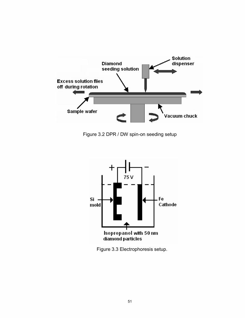
3.3.1.2 Diamond seeding set-ups
DPR and DW seeding methods employ regular photoresist spin on
technique, as shown in Figure 3.2. Sample wafers are put on a spinner (Model
WS-400B-6NPP/LITE, Laurell Tech. Corp.) and applied with DPR or DW solution.
Then, sample wafers will be spun at certain speeds (1000 rpm to 4000 rpm) for a
certain period of time (30s). The electrophoresis set-up is also very simple, as
shown in Figure 3.3. The sample will be suspended vertically in diamond loaded
Isopropanol solution. The separation between an iron cathode and the sample
anode is 1.5 cm. A +75 V bias (High Voltage DC Supply, Model 413C, John
Fluke) was applied to the sample for 30 or 60 minutes. The diamond particles will
gain negative surface charges when they suspend in organic solvents [86].
Therefore, the positive bias applied on the wafer has been shown to attract
negatively charged diamond particles. This seeding technique is especially
effective to seed diamond particles inside deep narrow Si channel.
51
Figure 3.2 DPR / DW spin-on seeding setup
Figure 3.3 Electrophoresis setup.
52
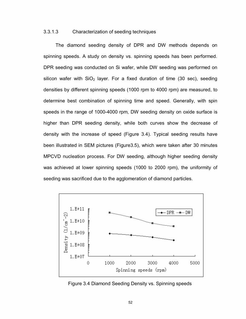
3.3.1.3 Characterization of seeding techniques
The diamond seeding density of DPR and DW methods depends on
spinning speeds. A study on density vs. spinning speeds has been performed.
DPR seeding was conducted on Si wafer, while DW seeding was performed on
silicon wafer with SiO2 layer. For a fixed duration of time (30 sec), seeding
densities by different spinning speeds (1000 rpm to 4000 rpm) are measured, to
determine best combination of spinning time and speed. Generally, with spin
speeds in the range of 1000-4000 rpm, DW seeding density on oxide surface is
higher than DPR seeding density, while both curves show the decrease of
density with the increase of speed (Figure 3.4). Typical seeding results have
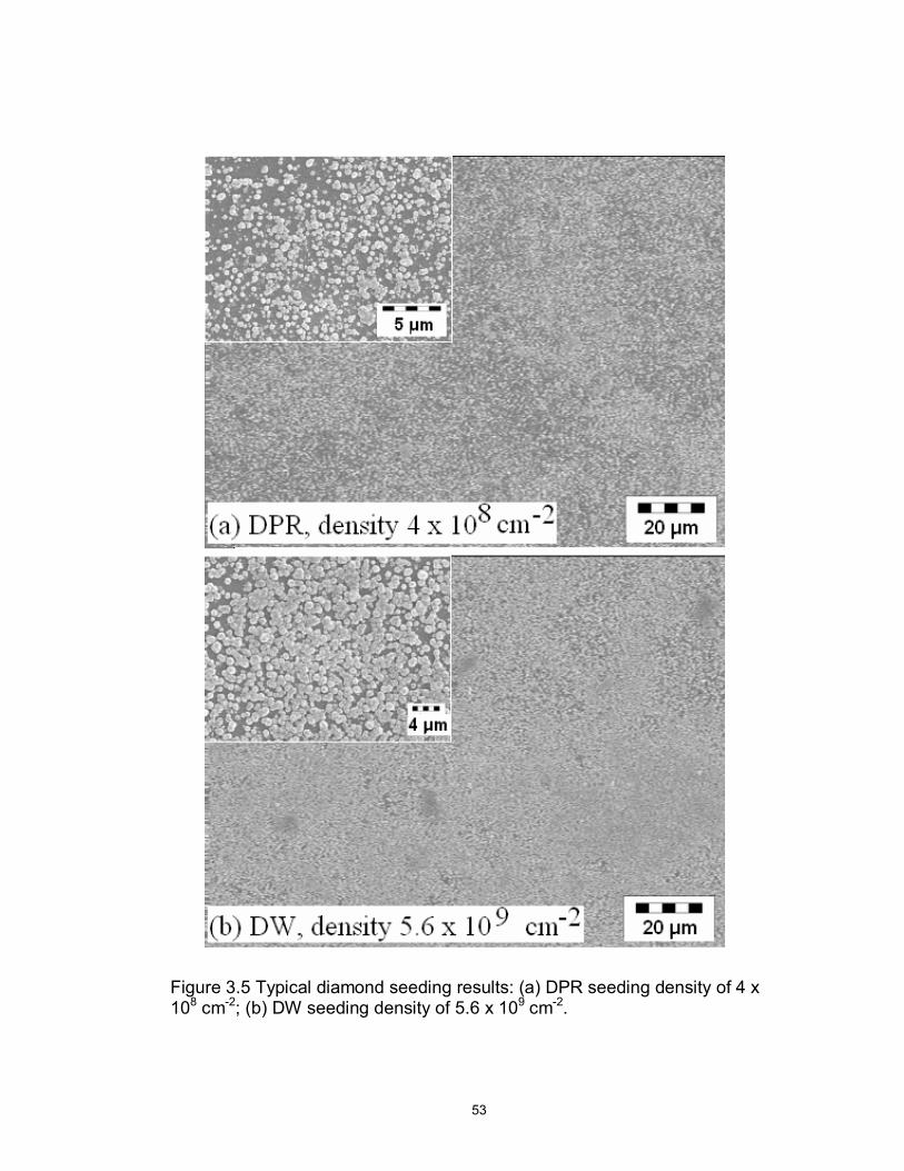
been illustrated in SEM pictures (Figure3.5), which were taken after 30 minutes
MPCVD nucleation process. For DW seeding, although higher seeding density
was achieved at lower spinning speeds (1000 to 2000 rpm), the uniformity of
seeding was sacrificed due to the agglomeration of diamond particles.
Figure 3.4 Diamond Seeding Density vs. Spinning speeds
53
Figure 3.5 Typical diamond seeding results: (a) DPR seeding density of 4 x 108 cm-2; (b) DW seeding density of 5.6 x 109 cm-2.
54
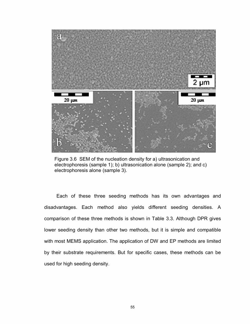
For electrophoresis method, different bias time and ultrasonication
combinations are tested to determine best seeding approach. During
electrophoresis seeding, ultrasonication was used to improve the seeding density.
After ultrasonication and electrophoresis, the wafers were allowed to dry in air.
Control wafers, using either ultrasonication or electrophoresis separately, were
also fabricated to see the effects on nucleation density. The treatment conditions
and diamond growth time of each sample are described in Table 3.2. The SEM
pictures in Figure 3.6 show the diamond nucleation density after 20 minutes of
MPCVD growth. The grain density is found to be 1.0 x 1010 cm-2 for sample 1; 8.0
x 109 cm-2 for sample 2; and 2.5 x 109 cm-2 for sample 3, after averaging over
many spots.. It should be noted that sample 2 and 3 had a very uneven particle
distribution, resulting in areas with high density and clumping, but mainly areas
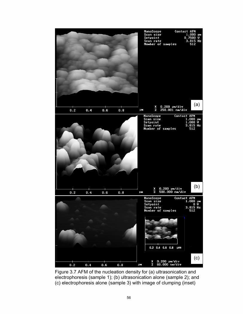
with no nucleation. The surface topography of these samples were stuied and
examined using AFM, as shown in Figure 3.7.
Table 3.2 Substrate Pretreatment Conditions and Diamond Growth Time
Sample Ultrasonication Time
[min]
Bias Time
[min]
MPCVD
Growth [hrs]
1 30 30 0.33
2 30 0 0.33
3 0 30 0.33
55
Each of these three seeding methods has its own advantages and
disadvantages. Each method also yields different seeding densities. A
comparison of these three methods is shown in Table 3.3. Although DPR gives
lower seeding density than other two methods, but it is simple and compatible
with most MEMS application. The application of DW and EP methods are limited
by their substrate requirements. But for specific cases, these methods can be
used for high seeding density.
Figure 3.6 SEM of the nucleation density for a) ultrasonication and electrophoresis (sample 1); b) ultrasonication alone (sample 2); and c) electrophoresis alone (sample 3).
56
(a)
(b)
(c)
Figure 3.7 AFM of the nucleation density for (a) ultrasonication and electrophoresis (sample 1); (b) ultrasonication alone (sample 2); and (c) electrophoresis alone (sample 3) with image of clumping (inset)
57
Table 3.3 Comparison of different seeding methods
Seeding method DPR spin EP bias /
Ultrasonic DW spin
Set-up Regular spinner Electrical setup Regular spinner
Substrate surface Most Dielectric &
metal Conductive Hydrophilic Surface
Uniformity and reproducibility
Good Good Good
Seeding density 108 ~ 10 9 cm-2 ~ 1010 cm-2 109 ~ 1010 cm-2
Advantages Simple, easy to use,
Fits for most MEMS
process.
High seeding
density,
Good at seeding
high aspect ratio
structures
Simple, easy to use,
High seeding density
on hydrophilic surface
Disadvantages
Density is lower than
other two method,
Diamond particles in
PR are tend to
cluster
Limited application Limited application
3.3.2 MPCVD poly-C deposition
MPCVD poly-C deposition is a very important step for poly-C thin film
technique. The deposition parameters of MPCVD will determine the quality of
poly-C thin film.
The driving force of this Ph.D. study is the excellent properties of diamond.
As for poly-C, the better film quality, the closer film characteristics are to that of
58
single crystalline diamond. It is very important to characterize MPCVD system
and optimize deposition parameters, to produce good quality film for poly-C
MEMS packaging application. When applying poly-C technique to MEMS
fabrication, low temperature poly-C deposition will be critical for temperature
compatible consideration.
3.3.2.1 Characterization of typical deposition parameters
Throughout this Ph.D. study, a MPCVD (Model MPDR 313EHP, Wavemat,
Inc.) system, with a cylindrical microwave cavity and a 5-inch quartz dome, was
used for diamond deposition. The 2.45 GHz, 5 kW SairemTM microwave power
supply and the large chamber size ensured the uniformity of plasma and the
poly-C deposition up to 4 inch size. The height of cylindrical cavity was set to
~21.59 cm, to operate in the electromagnetic mode designated TM013 for 2.45
GHz microwave. This mode was found to provide optimum film deposition
uniformity. Fine tunning of the cavity height should be performed during
deposition to reduce reflected microwave power. The sample wafer was heated
by the plasma and its temperature was monitored by an OMEGA pyrometer.
Typical MPCVD deposition parameters are listed in Table 3.4. Tri-methyl-boron
(B(OCH3)3, TMB) gas diluted in Hydrogen (TMB/H2 = 0.098% in volume ratio)
was introduced during the deposition for in-situ boron doping.
59
Table 3.4 Typical poly-C deposition parameters of MPCVD
Deposition Temperature (ºC) 450 ~ 800
Microwave Plasma Power (kW) 2.1 H2 100 CH4 1.5
Gas Flow Rate (sccm)
TMB 3 – 6 Deposition Chamber Pressure (torr) 40 - 50
From Table 3.4, microwave power and deposition pressure attribute to the
deposition temperature on sample surface, which is responsible for poly-C
deposition rate. The deposition pressure also affects the size of the plasma.
Higher pressure will constrain plasma to smaller size, resulting in smaller
deposition area. Lowering pressure will help to expand plasma size for larger
deposition area application. In addition to temperature, poly-C deposition rate is
also affected by the methane concentration in gas mixture. These deposition
parameters are characterized to explore the influences on poly-C deposition rate
and poly-C film quality.
3.3.2.2 Study of MPCVD deposition rate
Poly-C deposition rate varies with deposition temperature and gas
concentration. Figure 3.8 shows the calculated deposition rate varying with
deposition temperature. For this set of samples, gas concentration was set to
CH4/H2 = 1.5/100 sccm. Figure 3.9 shows the calculated deposition rate varying
60
with gas concentration. For this set of samples, deposition temperature was
controlled at 700 ºC (2 kW and 45 torr).
3.3.2.3 Study of MPCVD grown poly-C film quality
Diamond is formed by an infinite extension of sp3 carbon-carbon bonds.
However, since diamond is not a thermodynamically stable phase, much sp2-
bonded carbon often accompanies the CVD diamond deposition. The sensitivity
of Raman spectroscopy to even very small amounts of sp2 carbon makes it the
technique of choice to study these films. The sp3 bonding is indicated in Raman
spectra by the Raman shift at 1332 cm-1. For microcrystalline graphite (sp2
bonding), the first-order and second-order peak are at 1580 cm-1 and 1360 cm-1
respectively. But in CVD poly-C film, sp2 bonded carbon are highly disordered
graphite or amorphous carbon, which attribute to the features in Raman spectra
between 1350 and 1600 cm-1 [90]. Figure 3.10 illustrates the Raman spectra on
the poly-C films deposited under different temperatures with fixed gas
concentration. With the increase of growth temperature, Raman spectra show an
increase of diamond peak intensity and an intensity decrease in the sp2 featured
region, showing the improvement of film quality with higher deposition
temperature.
61
Figure 3.8 Deposition rate variations with temperature.
Figure 3.9 Deposition rate variations with gas concentrations.
62
Figure 3.10 Raman spectra of poly-C films grown at different temperatures.
63
3.3.2.4 Study of low temperature poly-C deposition
Although low temperature poly-C film deposition sacrifices the film quality, it
is also required for the compatibility with other fabrication process. Low
temperature deposition was performed in the range of 450 – 550 ºC, which is the
surface temperature in the center area of wafer. It was found that it is almost 100
ºC lower in temperature at the edge of the wafer. This feature limits the poly-C
growth in this area, resulting smaller effective deposition area. Figure 3.11 show
two poly-C films deposited at 475 ºC and 550 ºC respectively. Film #1 was
grown at 475 ºC for 12 hours to the thickness of 1 µm. The deposition rate is
around 0.083 µm/hr. Film #2 was grown at 550 ºC for 20 hours to the thickness
of 2.2 µm. The deposition rate is around 1.1 µm/hr.
Figure 3.11 Two poly-C films grown at low temperature: (a) 475 ºC and (b) 550
ºC.
64
3.3.3 Diamond doping technology
For p-type doping, Boron has shown to be a mostly used acceptor in
diamond. Boron acceptor level is 0.37 eV above the valence band. Although
doping in diamond may be accomplished during deposition, diffusion, or ion
implantation, there are some difficulties with diffusion doping and ion implantation.
Diffusion doping of diamond is difficult because of the low diffusivity in diamond
[91]. Boron diffusion depth of was only 50 nm. The boron diffusion coefficient in
diamond is 100 times smaller than the one in Si [92]. Ion implantation is also
difficult because of residual damage to the diamond [93]. If the damage exceeds
a critical threshold, then a subsequent anneal will produce graphite. Comparing
with these two doping techniques, Boron in-situ doping is much easier to control
and is reproducible [94][95].
However, obtaining n-type semiconducting diamond films by CVD has
proved more challenging, mainly due to the fact that suitable donor atoms such
as P, O, and As are larger than carbon, making incorporation into the diamond
lattice unfavorable. Also it lowers crystal quality. Nitrogen is a most common
impurity (donor) in diamond, but the resulting donor levels are too deep ~1.7 eV
almost 4 eV to conduction band.
In this study, boron in-situ doping was studied. Trimethylboron [B(CH3)3,
TMB] diluted in hydrogen (0.098%) was used as boron doping source of diamond
films, which was less toxic than B2H6. TMB is in the vapor state at room
temperature, and is easily diluted by argon, helium, hydrogen, nitrogen, and
silane gases.
65
3.3.3.1 Resistivity measurement of doped poly-C thin film
A four-point probe (Model S-301, Signatone) is used to measure the
resistivity of boron doped poly-C thin films, as shown in Figure 3.12. The probe
consists of four electrodes in line and separated by a distance s = 625 µm
(electrode-to-electrode). Current is driven through the outer two electrodes while
voltage is sensed on the inner electrodes. The sheet resistivity is calculated
based on the current source and sensed voltage. It then can be converted into
thin film bulk resistivity and sheet resistance.
For a film infinitely thin and of infinite extent (t<<s, d>>s, as shown above),
using a sheet resistivity denoted by sρ , then
rIEE
rIdensitycurrentJ s
rs
rr π
ρρπ 22
=⇒=== (3.1)
And,
Doped poly-C film
t
V
I
s s s
Probe
d
Figure 3.12 Four point probe measurement setup
66
( )rIdrEV srr ln
2πρ
== ∫ (3.2)
so the voltage drop V2 – V3 is given by
( ) ( ) ( ) ( )[ ]13232132 lnlnlnln2
ssssssIVVV s −++−+=−=πρ
(3.3)
and with s1=s2=s3=s4=s, then
( ) ( )[ ] ( )2lnln4ln2
2232 π
ρπρ ss IssIVVV =−=−= (3.4)
So, the sheet resistivity is
( )
=
=
IV
IV
s 53.42ln
πρ (3.5)
To account for the effects of finite thickness (t) and limited sample diameter
(d), correction factors (F, K) are used. Some of these are shown in Table 3.5.
⋅=
IVFKsρ (3.6)
To obtain the bulk resistivity of a film of thickness t, we multiply by the
thickness as
ts ⋅= ρρ (3.7)
The sheet resistance Rs (ohms/square) is then given as
ss
s tt
ttR ρ
ρρσ
====1 (3.8)
The resistivity of diamond decreased as the average grain size of the
diamond films decreased [96][97]. It was found that heavy doping was
67
deleterious in the early stage of diamond growth, but did not degrade growth on
an existing high quality diamond [98].
Table 3.5 Correction factors of some finite thickness and diameters
d/s K t/s F
3.0 2.266 0.4 0.9995
4.0 2.929 0.5 0.9975
5.0 3.363 0.625 0.9898
7.5 3.927 0.714 0.9798
10 4.172 0.833 0.9600
15 4.365 1.0 0.9214
20 4.436 1.25 0.8490
40 4.508 1.66 0.7225
100 4.532 2.0 0.6336
3.3.3.2 Resistivity variation with doping level and temperature
A set of sample was prepared with a layer of undoped poly-C deposition
(10 hours), followed by another two-hour doping deposition with different
TMB/CH4 ratios and different temperatures. The resistivity of each sample was
measure using four-point probe.
Figure 3.13 shows the relationship between poly-C film resisitivity and
different doping level, which is defined as the ratio of TMB over methane. As for
this set of experiments, the in-situ doping took place at temperature of 650 ºC.
The resistivity decreased as TMB / CH4 ratio increased and reached about 0.003
Ω⋅cm at heavy doping level (TMB/CH4 > 0.6%). The resistivity changes by nearly
four orders of magnitude
68
Figure 3.13 Doped poly-C film resistivity versus TMB/CH4 ratio.
Figure 3.14 illustrates the influence of deposition temperatures on thin film
resistivity. For light, medium or heavy doping, poly-C film resistivity decreased as
temperature increased. However, the resistivity change of light doping sample
relies on temperature much more than that of heavy doping.
Figure 3.14 Temperature dependence of poly-C film resisitivity.
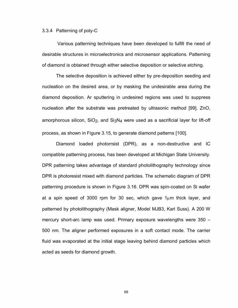
69
3.3.4 Patterning of poly-C
Various patterning techniques have been developed to fulfill the need of
desirable structures in microelectronics and microsensor applications. Patterning
of diamond is obtained through either selective deposition or selective etching.
The selective deposition is achieved either by pre-deposition seeding and
nucleation on the desired area, or by masking the undesirable area during the
diamond deposition. Ar sputtering in undesired regions was used to suppress
nucleation after the substrate was pretreated by ultrasonic method [99]. ZnO,
amorphorous silicon, SiO2, and Si3N4 were used as a sacrificial layer for lift-off
process, as shown in Figure 3.15, to generate diamond patterns [100].
Diamond loaded photorrsist (DPR), as a non-destructive and IC
compatible patterning process, has been developed at Michigan State University.
DPR patterning takes advantage of standard photolithography technology since
DPR is photoresist mixed with diamond particles. The schematic diagram of DPR
patterning procedure is shown in Figure 3.16. DPR was spin-coated on Si wafer
at a spin speed of 3000 rpm for 30 sec, which gave 1µm thick layer, and
patterned by photolithography (Mask aligner, Model MJB3, Karl Suss). A 200 W
mercury short-arc lamp was used. Primary exposure wavelengths were 350 –
500 nm. The aligner performed exposures in a soft contact mode. The carrier
fluid was evaporated at the initial stage leaving behind diamond particles which
acted as seeds for diamond growth.
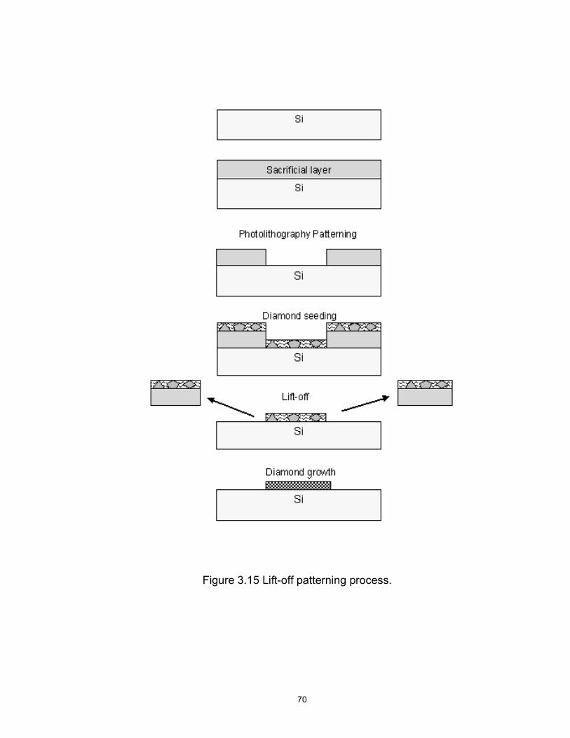
70
Figure 3.15 Lift-off patterning process.
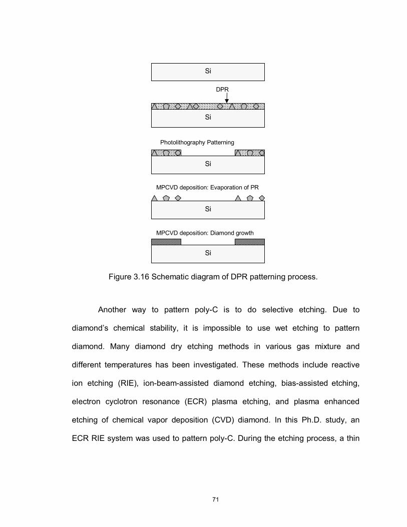
71
Another way to pattern poly-C is to do selective etching. Due to
diamond’s chemical stability, it is impossible to use wet etching to pattern
diamond. Many diamond dry etching methods in various gas mixture and
different temperatures has been investigated. These methods include reactive
ion etching (RIE), ion-beam-assisted diamond etching, bias-assisted etching,
electron cyclotron resonance (ECR) plasma etching, and plasma enhanced
etching of chemical vapor deposition (CVD) diamond. In this Ph.D. study, an
ECR RIE system was used to pattern poly-C. During the etching process, a thin
Si
Si
Si
Si
Si
DPR
Photolithography Patterning
MPCVD deposition: Evaporation of PR
MPCVD deposition: Diamond growth
Figure 3.16 Schematic diagram of DPR patterning process.
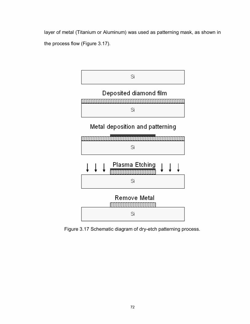
72
layer of metal (Titanium or Aluminum) was used as patterning mask, as shown in
the process flow (Figure 3.17).
Figure 3.17 Schematic diagram of dry-etch patterning process.
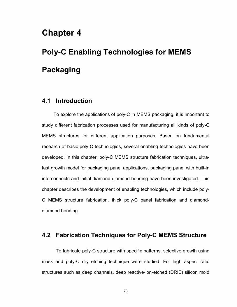
73
Chapter 4
Poly-C Enabling Technologies for MEMS
Packaging
4.1 Introduction
To explore the applications of poly-C in MEMS packaging, it is important to
study different fabrication processes used for manufacturing all kinds of poly-C
MEMS structures for different application purposes. Based on fundamental
research of basic poly-C technologies, several enabling technologies have been
developed. In this chapter, poly-C MEMS structure fabrication techniques, ultra-
fast growth model for packaging panel applications, packaging panel with built-in
interconnects and initial diamond-diamond bonding have been investigated. This
chapter describes the development of enabling technologies, which include poly-
C MEMS structure fabrication, thick poly-C panel fabrication and diamond-
diamond bonding.
4.2 Fabrication Techniques for Poly-C MEMS Structure
To fabricate poly-C structure with specific patterns, selective growth using
mask and poly-C dry etching technique were studied. For high aspect ratio
structures such as deep channels, deep reactive-ion-etched (DRIE) silicon mold
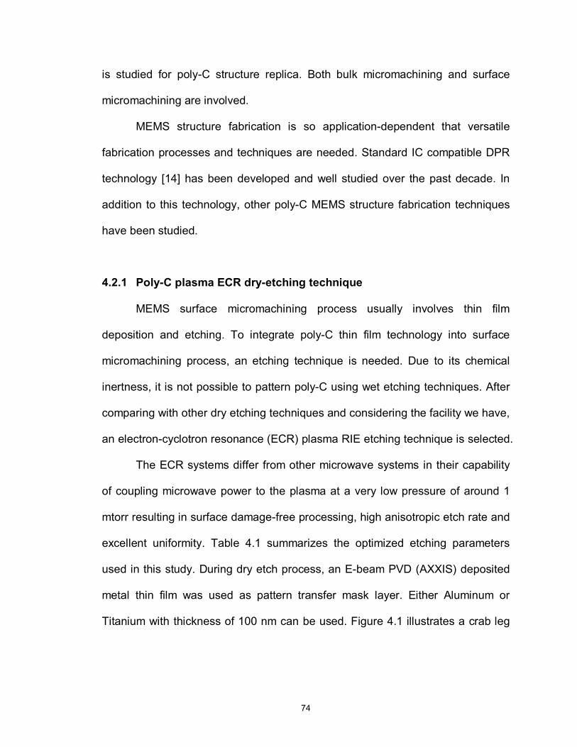
74
is studied for poly-C structure replica. Both bulk micromachining and surface
micromachining are involved.
MEMS structure fabrication is so application-dependent that versatile
fabrication processes and techniques are needed. Standard IC compatible DPR
technology [14] has been developed and well studied over the past decade. In
addition to this technology, other poly-C MEMS structure fabrication techniques
have been studied.
4.2.1 Poly-C plasma ECR dry-etching technique
MEMS surface micromachining process usually involves thin film
deposition and etching. To integrate poly-C thin film technology into surface
micromachining process, an etching technique is needed. Due to its chemical
inertness, it is not possible to pattern poly-C using wet etching techniques. After
comparing with other dry etching techniques and considering the facility we have,
an electron-cyclotron resonance (ECR) plasma RIE etching technique is selected.
The ECR systems differ from other microwave systems in their capability
of coupling microwave power to the plasma at a very low pressure of around 1
mtorr resulting in surface damage-free processing, high anisotropic etch rate and
excellent uniformity. Table 4.1 summarizes the optimized etching parameters
used in this study. During dry etch process, an E-beam PVD (AXXIS) deposited
metal thin film was used as pattern transfer mask layer. Either Aluminum or
Titanium with thickness of 100 nm can be used. Figure 4.1 illustrates a crab leg
75
accelerometer that was patterned using ECR plasma dry etching. The inset
picture shows the details of the edge of patterned structure.
Table 4.1 ECR plasma etching parameters
Ar 8.0 O2 28.0
Gas Flow Rate (sccm) SF6 2.0
Microwave Input Power (W) 400
RF Power (W) 100
DC Bias (V) -130
Chamber pressure (mtorr) 5
Typical Etch Rate (µm/hour) 4.5
Figure 4.1 SEM picture of a poly-C crab-leg accelerometer patterned using dry-etching technique; inset is a close view of etched edge.
200 µm
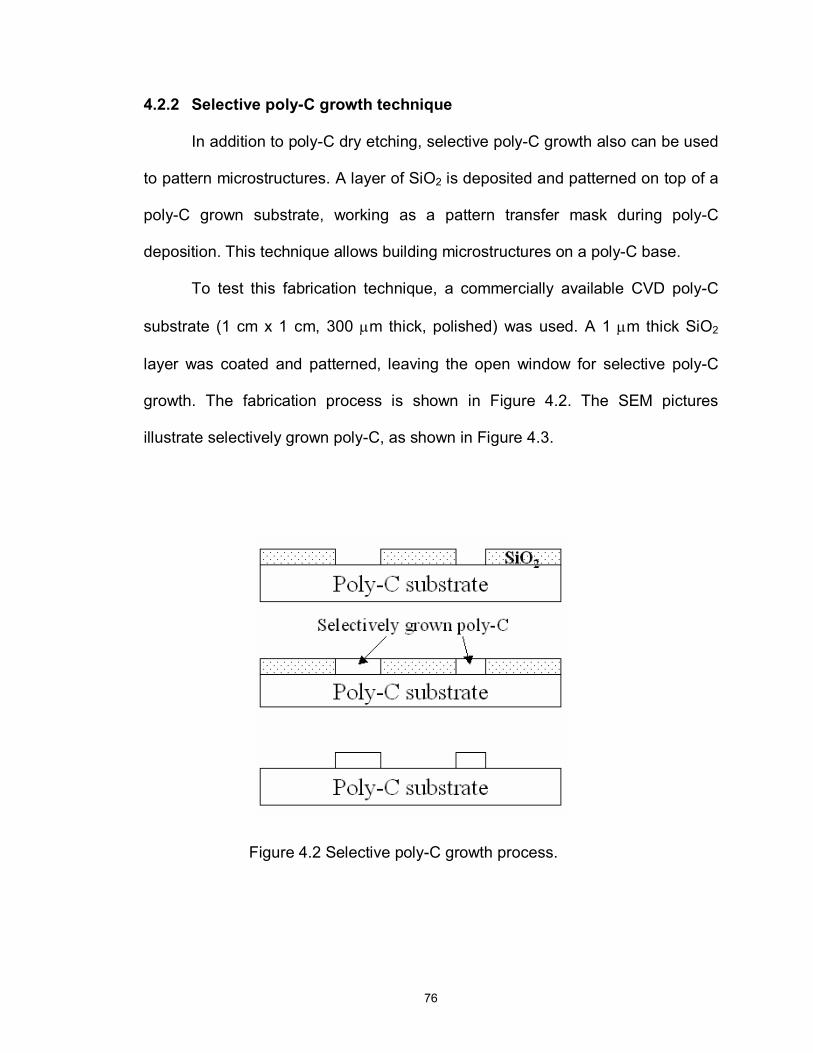
76
4.2.2 Selective poly-C growth technique
In addition to poly-C dry etching, selective poly-C growth also can be used
to pattern microstructures. A layer of SiO2 is deposited and patterned on top of a
poly-C grown substrate, working as a pattern transfer mask during poly-C
deposition. This technique allows building microstructures on a poly-C base.
To test this fabrication technique, a commercially available CVD poly-C
substrate (1 cm x 1 cm, 300 µm thick, polished) was used. A 1 µm thick SiO2
layer was coated and patterned, leaving the open window for selective poly-C
growth. The fabrication process is shown in Figure 4.2. The SEM pictures
illustrate selectively grown poly-C, as shown in Figure 4.3.
Figure 4.2 Selective poly-C growth process.
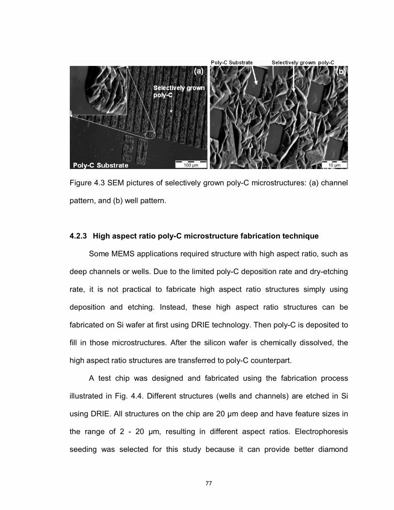
77
Figure 4.3 SEM pictures of selectively grown poly-C microstructures: (a) channel
pattern, and (b) well pattern.
4.2.3 High aspect ratio poly-C microstructure fabrication technique
Some MEMS applications required structure with high aspect ratio, such as
deep channels or wells. Due to the limited poly-C deposition rate and dry-etching
rate, it is not practical to fabricate high aspect ratio structures simply using
deposition and etching. Instead, these high aspect ratio structures can be
fabricated on Si wafer at first using DRIE technology. Then poly-C is deposited to
fill in those microstructures. After the silicon wafer is chemically dissolved, the
high aspect ratio structures are transferred to poly-C counterpart.
A test chip was designed and fabricated using the fabrication process
illustrated in Fig. 4.4. Different structures (wells and channels) are etched in Si
using DRIE. All structures on the chip are 20 µm deep and have feature sizes in
the range of 2 - 20 µm, resulting in different aspect ratios. Electrophoresis
seeding was selected for this study because it can provide better diamond
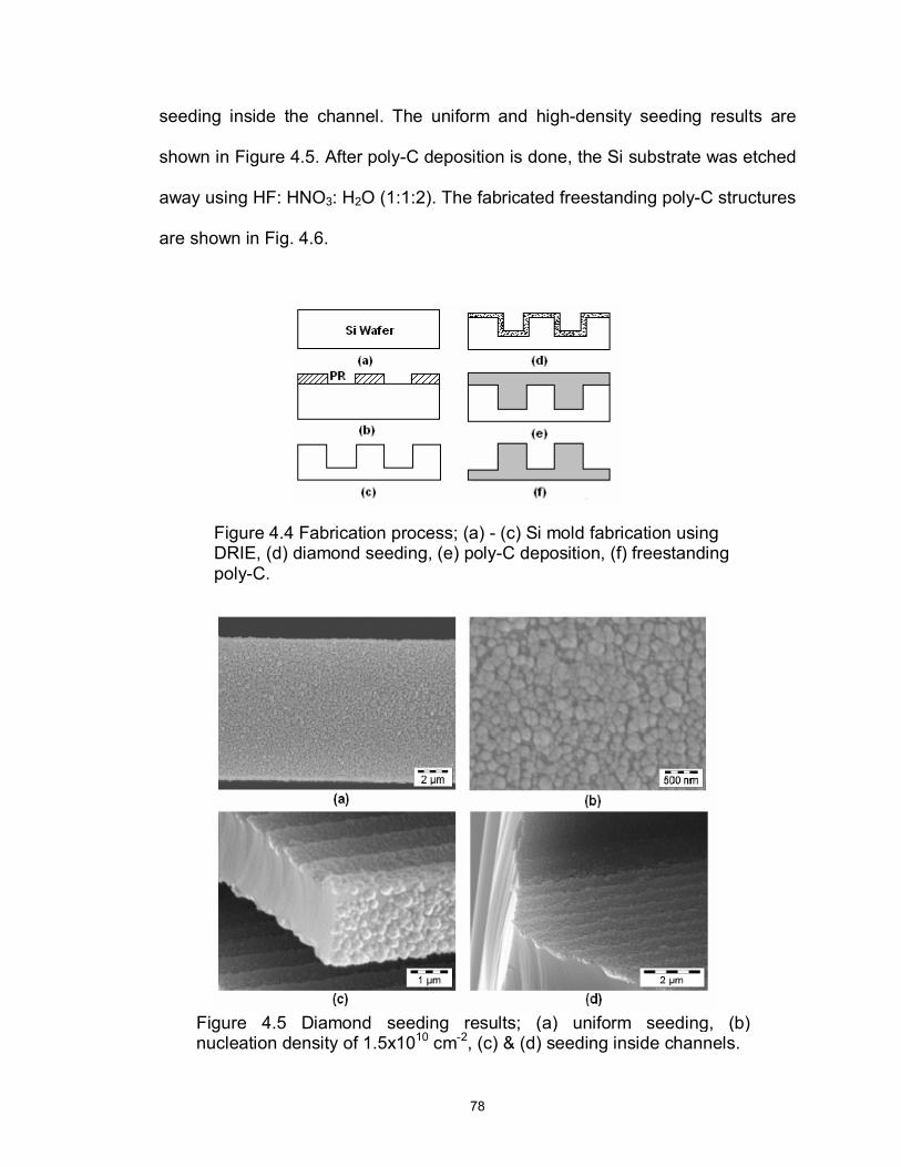
78
seeding inside the channel. The uniform and high-density seeding results are
shown in Figure 4.5. After poly-C deposition is done, the Si substrate was etched
away using HF: HNO3: H2O (1:1:2). The fabricated freestanding poly-C structures
are shown in Fig. 4.6.
Figure 4.5 Diamond seeding results; (a) uniform seeding, (b) nucleation density of 1.5x1010 cm-2, (c) & (d) seeding inside channels.
Figure 4.4 Fabrication process; (a) - (c) Si mold fabrication using DRIE, (d) diamond seeding, (e) poly-C deposition, (f) freestanding poly-C.
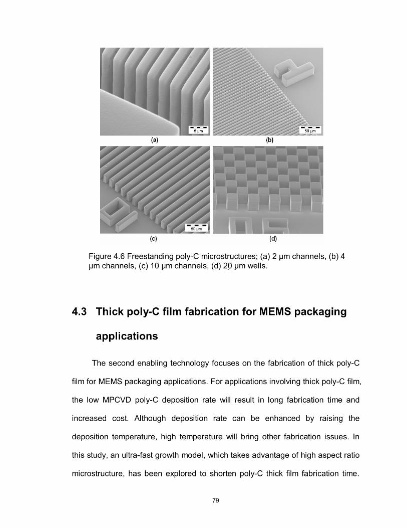
79
4.3 Thick poly-C film fabrication for MEMS packaging
applications
The second enabling technology focuses on the fabrication of thick poly-C
film for MEMS packaging applications. For applications involving thick poly-C film,
the low MPCVD poly-C deposition rate will result in long fabrication time and
increased cost. Although deposition rate can be enhanced by raising the
deposition temperature, high temperature will bring other fabrication issues. In
this study, an ultra-fast growth model, which takes advantage of high aspect ratio
microstructure, has been explored to shorten poly-C thick film fabrication time.
Figure 4.6 Freestanding poly-C microstructures; (a) 2 µm channels, (b) 4 µm channels, (c) 10 µm channels, (d) 20 µm wells.
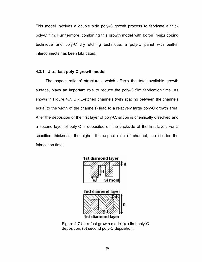
80
This model involves a double side poly-C growth process to fabricate a thick
poly-C film. Furthermore, combining this growth model with boron in-situ doping
technique and poly-C dry etching technique, a poly-C panel with built-in
interconnects has been fabricated.
4.3.1 Ultra fast poly-C growth model
The aspect ratio of structures, which affects the total available growth
surface, plays an important role to reduce the poly-C film fabrication time. As
shown in Figure 4.7, DRIE-etched channels (with spacing between the channels
equal to the width of the channels) lead to a relatively large poly-C growth area.
After the deposition of the first layer of poly-C, silicon is chemically dissolved and
a second layer of poly-C is deposited on the backside of the first layer. For a
specified thickness, the higher the aspect ratio of channel, the shorter the
fabrication time.
Figure 4.7 Ultra-fast growth model; (a) first poly-C deposition, (b) second poly-C deposition.
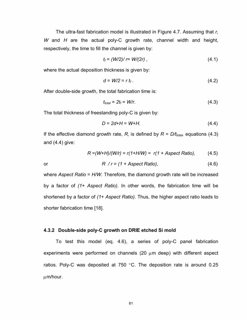
81
The ultra-fast fabrication model is illustrated in Figure 4.7. Assuming that r,
W and H are the actual poly-C growth rate, channel width and height,
respectively, the time to fill the channel is given by:
tf = (W/2)/ r= W/(2r) , (4.1)
where the actual deposition thickness is given by:
d = W/2 = r tf . (4.2)
After double-side growth, the total fabrication time is:
ttotal = 2tf = W/r. (4.3)
The total thickness of freestanding poly-C is given by:
D = 2d+H = W+H. (4.4)
If the effective diamond growth rate, R, is defined by R = D/ttotal, equations (4.3)
and (4.4) give:
R =(W+H)/(W/r) = r(1+H/W) = r(1 + Aspect Ratio), (4.5)
or R / r = (1 + Aspect Ratio), (4.6)
where Aspect Ratio = H/W. Therefore, the diamond growth rate will be increased
by a factor of (1+ Aspect Ratio). In other words, the fabrication time will be
shortened by a factor of (1+ Aspect Ratio). Thus, the higher aspect ratio leads to
shorter fabrication time [18].
4.3.2 Double-side poly-C growth on DRIE etched Si mold
To test this model (eq. 4.6), a series of poly-C panel fabrication
experiments were performed on channels (20 µm deep) with different aspect
ratios. Poly-C was deposited at 750 °C. The deposition rate is around 0.25
µm/hour.
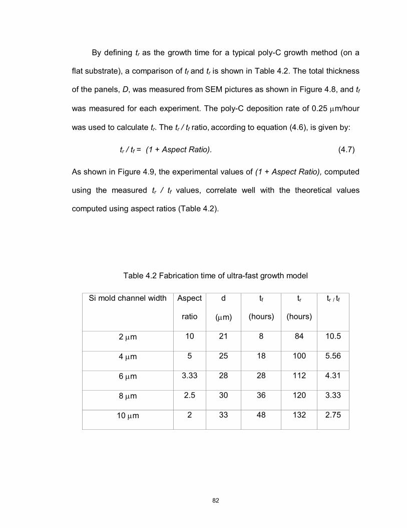
82
By defining tr as the growth time for a typical poly-C growth method (on a
flat substrate), a comparison of tf and tr is shown in Table 4.2. The total thickness
of the panels, D, was measured from SEM pictures as shown in Figure 4.8, and tf
was measured for each experiment. The poly-C deposition rate of 0.25 µm/hour
was used to calculate tr. The tr / tf ratio, according to equation (4.6), is given by:
tr / tf = (1 + Aspect Ratio). (4.7)
As shown in Figure 4.9, the experimental values of (1 + Aspect Ratio), computed
using the measured tr / tf values, correlate well with the theoretical values
computed using aspect ratios (Table 4.2).
Table 4.2 Fabrication time of ultra-fast growth model
Si mold channel width Aspect
ratio
d
(µm)
tf
(hours)
tr
(hours)
tr / tf
2 µm 10 21 8 84 10.5
4 µm 5 25 18 100 5.56
6 µm 3.33 28 28 112 4.31
8 µm 2.5 30 36 120 3.33
10 µm 2 33 48 132 2.75
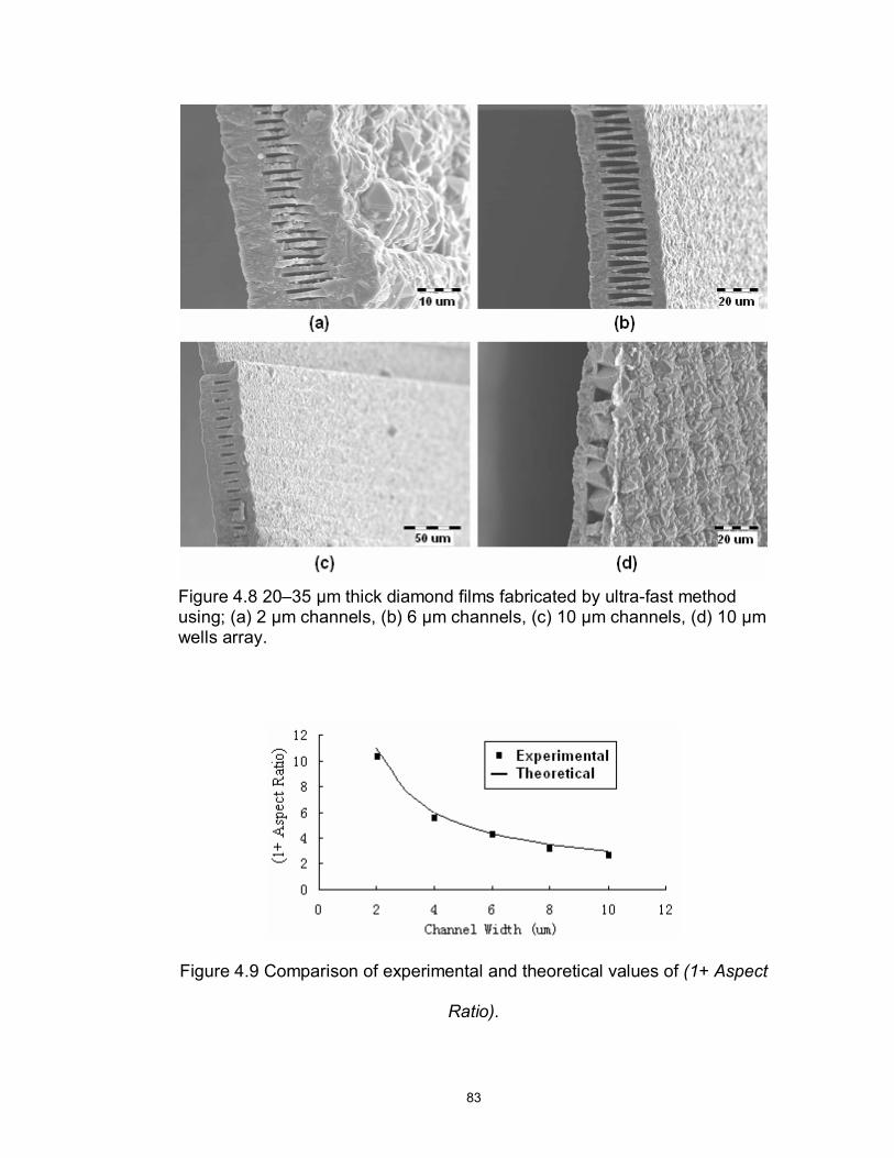
83
Figure 4.9 Comparison of experimental and theoretical values of (1+ Aspect
Ratio).
Figure 4.8 20–35 µm thick diamond films fabricated by ultra-fast method using; (a) 2 µm channels, (b) 6 µm channels, (c) 10 µm channels, (d) 10 µm wells array.
84
A unique contribution of this study is that the developed ultra-fast model
can shorten the thick panel fabrication time significantly, providing a new concept
of improving poly-C deposition efficiency [18].
4.3.3 Filling of silicon mold
Area that requires an improvement in the current work is the partial filling of
Si molds for channels with high aspect ratios. Figure 4.8 reveals key-holes (voids)
formed in the high-aspect ratio channels due to the increasing edge effect
restricting the transportation of growth-related plasma species into the bottom
areas of the channels. This pre-mature filling of high aspect ratio channels,
though a problem for the fast growth process, can lead to poly-C channels for
micro-fluidic applications [101]. To find the highest aspect ratio of a channel
which yields best poly-C filling, a study was conducted to deposit poly-C inside
channels with aspect ratios in the range of 1 - 10. As shown in Figure 4.10 (a)
and (b), channels with aspect ratio < 3 can be totally filled but the channels with
higher aspect ratios lead to voids as see in Figure 4.10 (c) and (d). Therefore, to
fabricate a poly-C panel with complete filling, channels with aspect ratio less than
3 should be applied to avoid any reliability concerns.
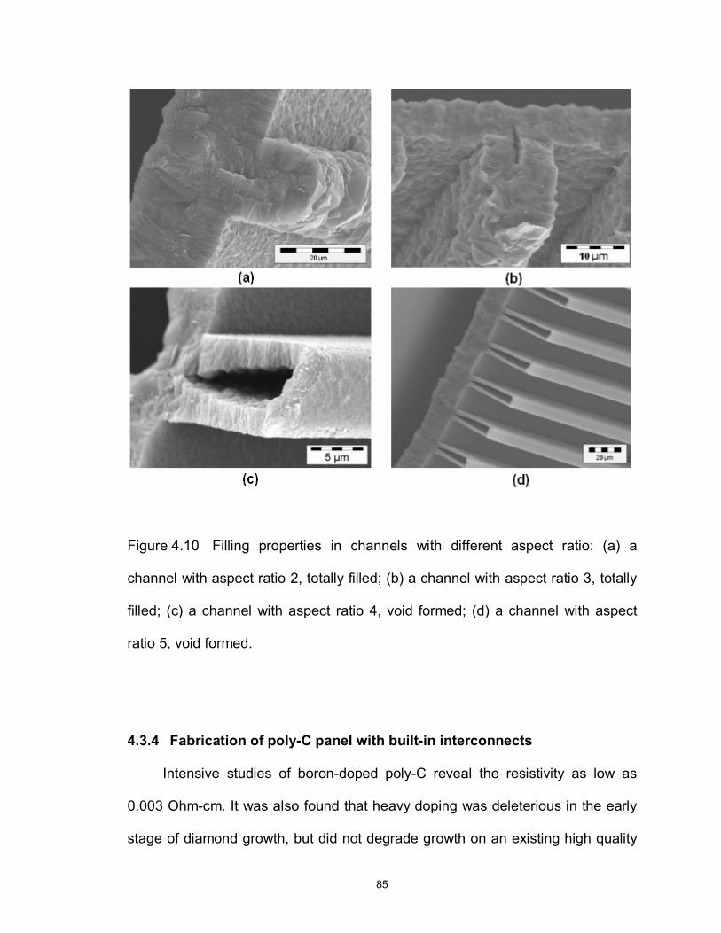
85
Figure 4.10 Filling properties in channels with different aspect ratio: (a) a
channel with aspect ratio 2, totally filled; (b) a channel with aspect ratio 3, totally
filled; (c) a channel with aspect ratio 4, void formed; (d) a channel with aspect
ratio 5, void formed.
4.3.4 Fabrication of poly-C panel with built-in interconnects
Intensive studies of boron-doped poly-C reveal the resistivity as low as
0.003 Ohm-cm. It was also found that heavy doping was deleterious in the early
stage of diamond growth, but did not degrade growth on an existing high quality
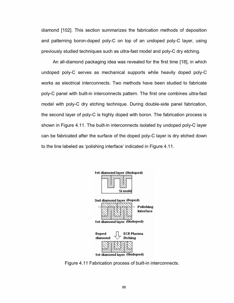
86
diamond [102]. This section summarizes the fabrication methods of deposition
and patterning boron-doped poly-C on top of an undoped poly-C layer, using
previously studied techniques such as ultra-fast model and poly-C dry etching.
An all-diamond packaging idea was revealed for the first time [18], in which
undoped poly-C serves as mechanical supports while heavily doped poly-C
works as electrical interconnects. Two methods have been studied to fabricate
poly-C panel with built-in interconnects pattern. The first one combines ultra-fast
model with poly-C dry etching technique. During double-side panel fabrication,
the second layer of poly-C is highly doped with boron. The fabrication process is
shown in Figure 4.11. The built-in interconnects isolated by undoped poly-C layer
can be fabricated after the surface of the doped poly-C layer is dry etched down
to the line labeled as ‘polishing interface’ indicated in Figure 4.11.
Figure 4.11 Fabrication process of built-in interconnects.
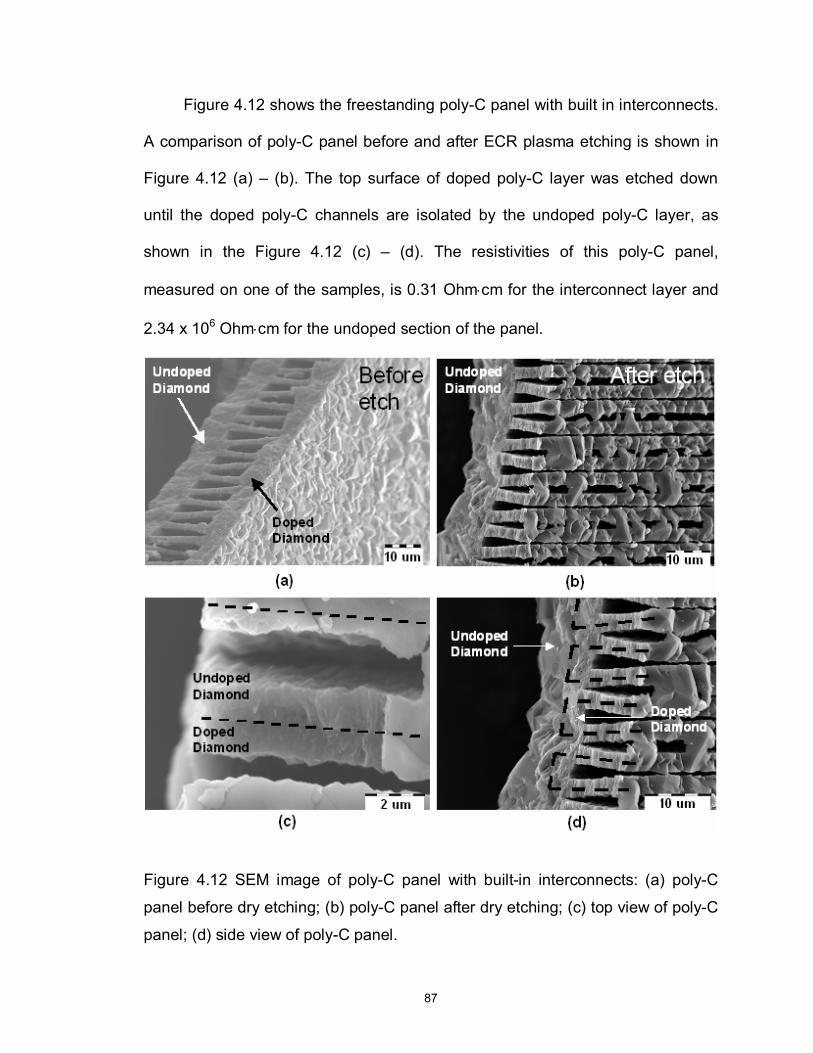
87
Figure 4.12 shows the freestanding poly-C panel with built in interconnects.
A comparison of poly-C panel before and after ECR plasma etching is shown in
Figure 4.12 (a) – (b). The top surface of doped poly-C layer was etched down
until the doped poly-C channels are isolated by the undoped poly-C layer, as
shown in the Figure 4.12 (c) – (d). The resistivities of this poly-C panel,
measured on one of the samples, is 0.31 Ohm⋅cm for the interconnect layer and
2.34 x 10⁶ Ohm⋅cm for the undoped section of the panel.
Figure 4.12 SEM image of poly-C panel with built-in interconnects: (a) poly-C
panel before dry etching; (b) poly-C panel after dry etching; (c) top view of poly-C
panel; (d) side view of poly-C panel.
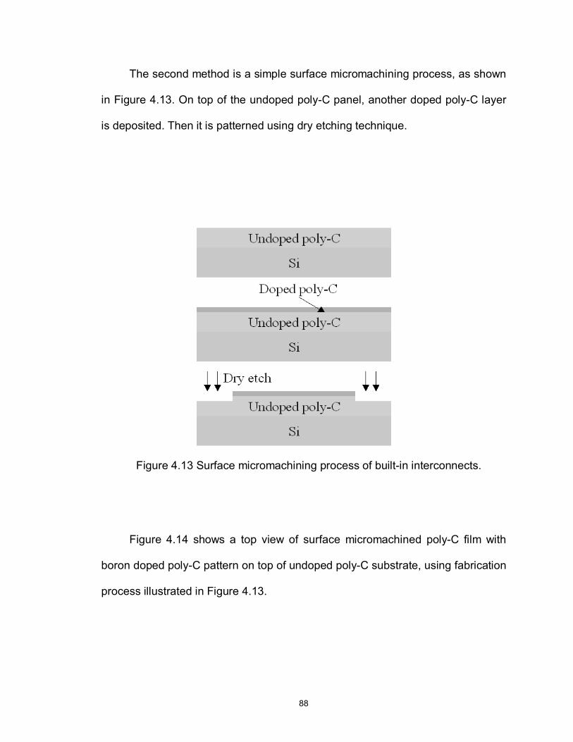
88
The second method is a simple surface micromachining process, as shown
in Figure 4.13. On top of the undoped poly-C panel, another doped poly-C layer
is deposited. Then it is patterned using dry etching technique.
Figure 4.14 shows a top view of surface micromachined poly-C film with
boron doped poly-C pattern on top of undoped poly-C substrate, using fabrication
process illustrated in Figure 4.13.
Figure 4.13 Surface micromachining process of built-in interconnects.
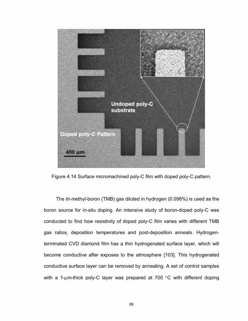
89
Figure 4.14 Surface micromachined poly-C film with doped poly-C pattern.
The tri-methyl-boron (TMB) gas diluted in hydrogen (0.098%) is used as the
boron source for in-situ doping. An intensive study of boron-doped poly-C was
conducted to find how resistivity of doped poly-C film varies with different TMB
gas ratios, deposition temperatures and post-deposition anneals. Hydrogen-
terminated CVD diamond film has a thin hydrogenated surface layer, which will
become conductive after exposes to the atmosphere [103]. This hydrogenated
conductive surface layer can be removed by annealing. A set of control samples
with a 1-µm-thick poly-C layer was prepared at 700 °C with different doping
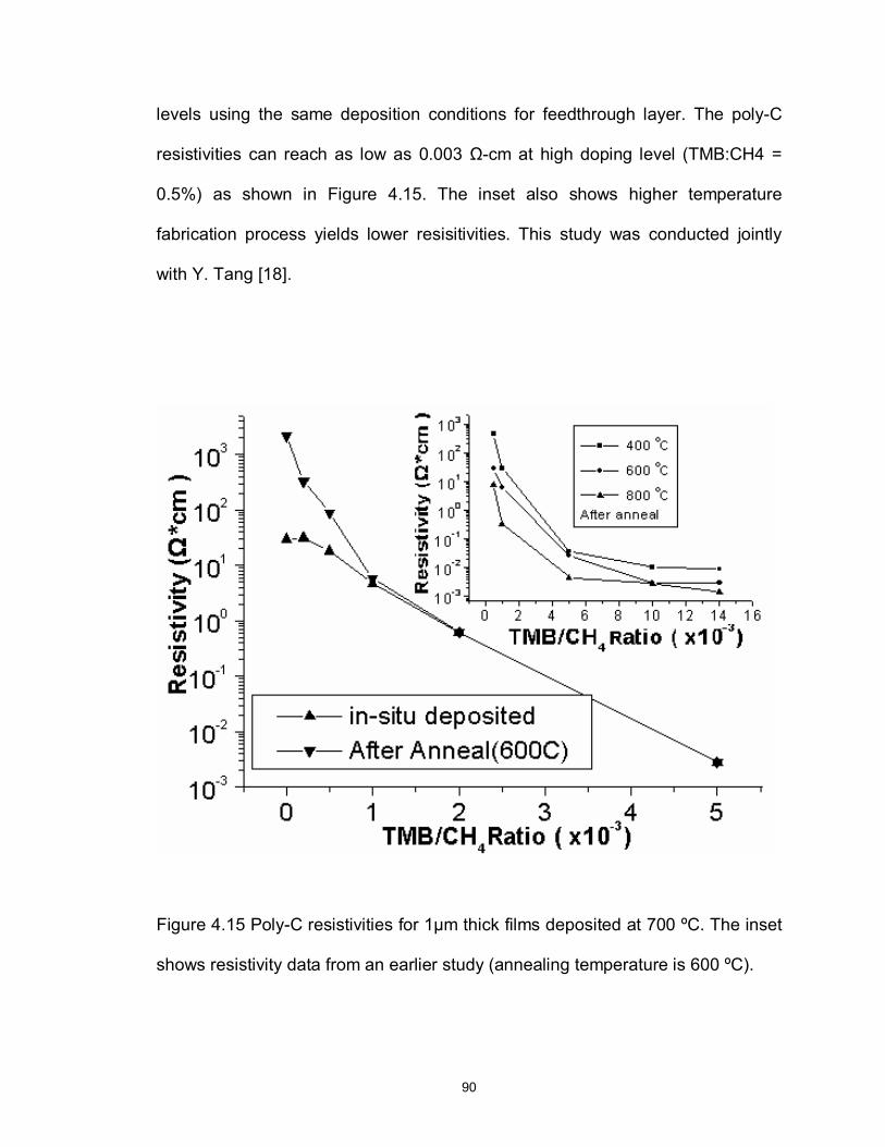
90
levels using the same deposition conditions for feedthrough layer. The poly-C
resistivities can reach as low as 0.003 Ω-cm at high doping level (TMB:CH4 =
0.5%) as shown in Figure 4.15. The inset also shows higher temperature
fabrication process yields lower resisitivities. This study was conducted jointly
with Y. Tang [18].
Figure 4.15 Poly-C resistivities for 1μm thick films deposited at 700 ºC. The inset
shows resistivity data from an earlier study (annealing temperature is 600 ºC).
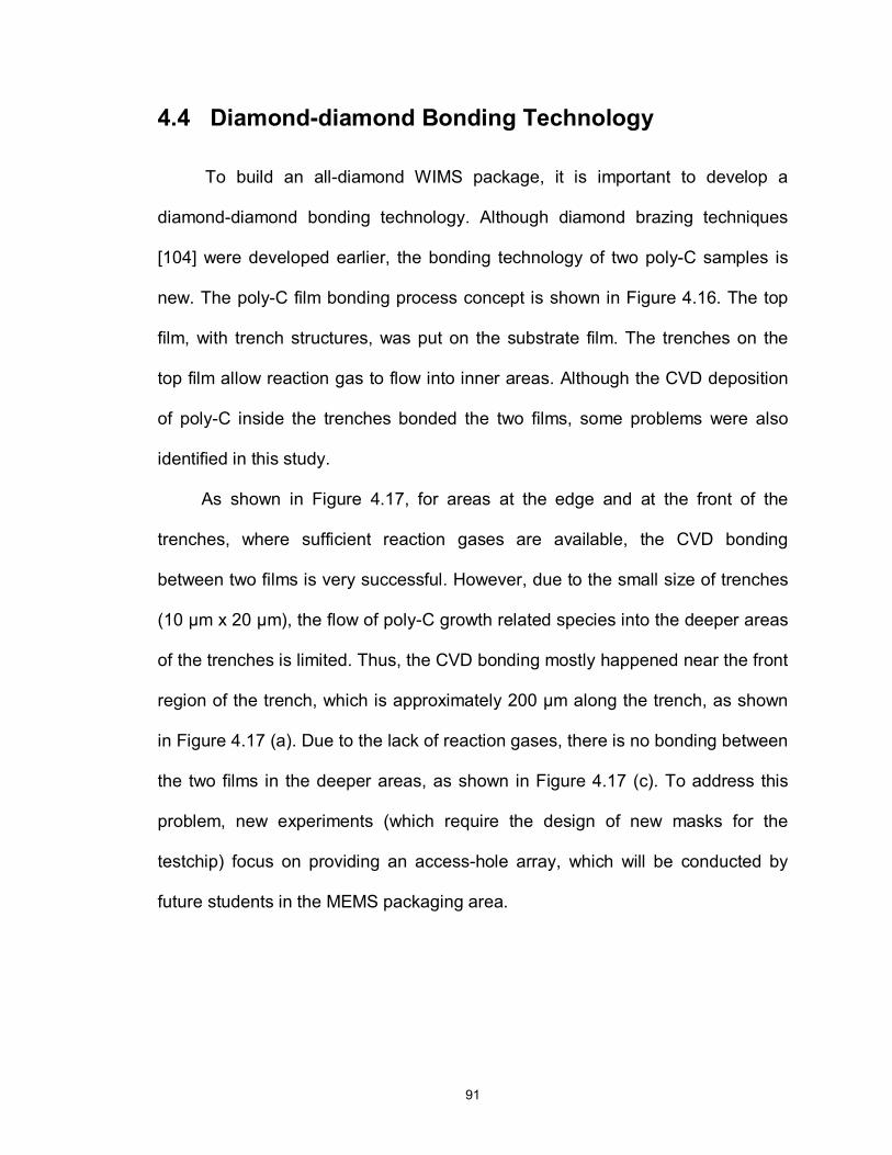
91
4.4 Diamond-diamond Bonding Technology
To build an all-diamond WIMS package, it is important to develop a
diamond-diamond bonding technology. Although diamond brazing techniques
[104] were developed earlier, the bonding technology of two poly-C samples is
new. The poly-C film bonding process concept is shown in Figure 4.16. The top
film, with trench structures, was put on the substrate film. The trenches on the
top film allow reaction gas to flow into inner areas. Although the CVD deposition
of poly-C inside the trenches bonded the two films, some problems were also
identified in this study.
As shown in Figure 4.17, for areas at the edge and at the front of the
trenches, where sufficient reaction gases are available, the CVD bonding
between two films is very successful. However, due to the small size of trenches
(10 μm x 20 μm), the flow of poly-C growth related species into the deeper areas
of the trenches is limited. Thus, the CVD bonding mostly happened near the front
region of the trench, which is approximately 200 μm along the trench, as shown
in Figure 4.17 (a). Due to the lack of reaction gases, there is no bonding between
the two films in the deeper areas, as shown in Figure 4.17 (c). To address this
problem, new experiments (which require the design of new masks for the
testchip) focus on providing an access-hole array, which will be conducted by
future students in the MEMS packaging area.
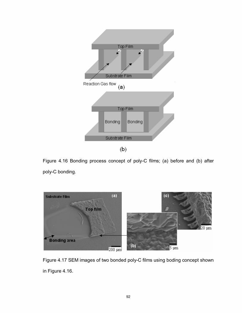
92
Figure 4.16 Bonding process concept of poly-C films; (a) before and (b) after
poly-C bonding.
Figure 4.17 SEM images of two bonded poly-C films using boding concept shown
in Figure 4.16.
93
Chapter 5
Poly-C Thin Film Encapsulation Packaging
5.1 Introduction
Although MEMS packaging can take advantage of mature packaging
techniques from semiconductor IC industry, MEMS packaging is still complicated
due to the diversity of applications. Recently, the developments in MEMS area
have led to growing interests in MEMS packaging at wafer level to reduce the
packaging and testing cost. Meanwhile, poly-C draws more and more attention in
packaging area because of its excellent thermal, mechanical, chemical and
electrical properties.
As mentioned in Chapter 1, this Ph.D. study has two parallel research
directions: poly-C packaging panel fabrication and integrated poly-C thin film
encapsulation process. As shown in Figure 1.1. While several enabling poly-C
MEMS packaging technologies have been developed for both research directions,
this dissertation has an emphasis on the poly-C thin film encapsulation
packaging process. This chapter summarizes the development of poly-C thin film
encapsulation packaging, including material selection, process design, test
package fabrication and evaluation.
94
5.2 Poly-C Thin Film Packaging Process Design
Generally, MEMS packages are expected to provide micro-devices and on-
chip circuits with functions such as mechanical support, protection from
environment, electrical interconnection and thermal management. Due to its
extreme hardness, chemical and mechanical stability, large band gap, and
highest thermal conductivity, poly-C is emerging as a novel sensor material for
MEMS applications. The high Young’s modulus and chemical stability of poly-C
make it an excellent candidate material for thin film package.
In previous chapter, it has been proven that poly-C thin film technology can
be easily incorporated into surface micromachining process. Therefore, poly-C
thin film technology can be integrated with MEMS fabrication process and
provide MEMS device and even on-chip circuits a package shell for mechanical
and chemical protection (as shown in Figure 5.1).
This section presents the design procedure of poly-C thin film packaging
technology that applies developed enabling poly-C MEMS technologies to post-
MEMS encapsulation packaging process.
5.2.1 Packaging material consideration
The material of thin film package should possess excellent properties. As
for mechanical consideration, the thin film package must be designed to
withstand certain differential pressure. According to the model proposed by
Maier–Schneider [105], the pressure load-deflection relationship of thin film
package is given by,
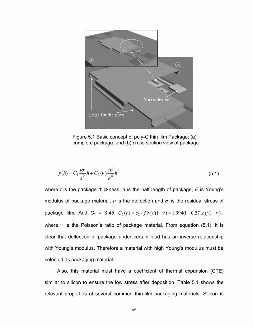
95
34221 )()( h
atECh
atChp νσ
+= (5.1)
where t is the package thickness, a is the half length of package, E is Young’s
modulus of package material, h is the deflection and σ is the residual stress of
package film. And C1 = 3.45, )1()271.01(994.1)1/()()( 22 ννννν −−=−⋅= fcC ,
where ν is the Poisson’s ratio of package material. From equation (5.1), it is
clear that deflection of package under certain load has an inverse relationship
with Young’s modulus. Therefore a material with high Young’s modulus must be
selected as packaging material.
Also, this material must have a coefficient of thermal expansion (CTE)
similar to silicon to ensure the low stress after deposition. Table 5.1 shows the
relevant properties of several common thin-film packaging materials. Silicon is
Figure 5.1 Basic concept of poly-C thin film Package: (a) complete package, and (b) cross section view of package.
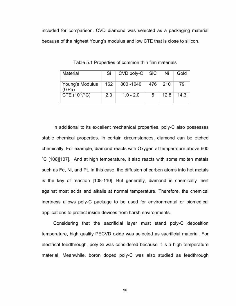
96
included for comparison. CVD diamond was selected as a packaging material
because of the highest Young’s modulus and low CTE that is close to silicon.
Table 5.1 Properties of common thin film materials
Material Si CVD poly-C SiC Ni Gold
Young’s Modulus (GPa)
162 800 -1040 476 210 79
CTE (10-6/°C) 2.3 1.0 - 2.0 5 12.8 14.3
In additional to its excellent mechanical properties, poly-C also possesses
stable chemical properties. In certain circumstances, diamond can be etched
chemically. For example, diamond reacts with Oxygen at temperature above 600
ºC [106][107]. And at high temperature, it also reacts with some molten metals
such as Fe, Ni, and Pt. In this case, the diffusion of carbon atoms into hot metals
is the key of reaction [108-110]. But generally, diamond is chemically inert
against most acids and alkalis at normal temperature. Therefore, the chemical
inertness allows poly-C package to be used for environmental or biomedical
applications to protect inside devices from harsh environments.
Considering that the sacrificial layer must stand poly-C deposition
temperature, high quality PECVD oxide was selected as sacrificial material. For
electrical feedthrough, poly-Si was considered because it is a high temperature
material. Meanwhile, boron doped poly-C was also studied as feedthrough
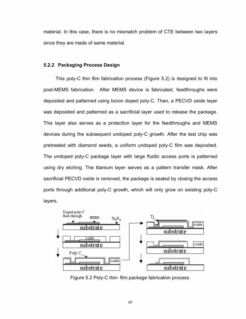
97
material. In this case, there is no mismatch problem of CTE between two layers
since they are made of same material.
5.2.2 Packaging Process Design
This poly-C thin film fabrication process (Figure 5.2) is designed to fit into
post-MEMS fabrication. After MEMS device is fabricated, feedthroughs were
deposited and patterned using boron doped poly-C. Then, a PECVD oxide layer
was deposited and patterned as a sacrificial layer used to release the package.
This layer also serves as a protection layer for the feedthroughs and MEMS
devices during the subsequent undoped poly-C growth. After the test chip was
pretreated with diamond seeds, a uniform undoped poly-C film was deposited.
The undoped poly-C package layer with large fluidic access ports is patterned
using dry etching. The titanium layer serves as a pattern transfer mask. After
sacrificial PECVD oxide is removed, the package is sealed by closing the access
ports through additional poly-C growth, which will only grow on existing poly-C
layers.
Figure 5.2 Poly-C thin- film package fabrication process.
98
5.3 Fabrication of Poly-C Package
5.3.1 Poly-C thin film fabrication for packaging
A typical poly-C film fabrication involves seeding, growth, doping and
patterning. Seeding is a pretreatment step to generate diamond nuclei before
diamond growth begins. Three currently used seeding methods, diamond-loaded
photoresist, diamond-loaded water and electrophoresis, have been studied and
summarized in Chapter 3. Each seeding method applies on different substrate
and yields different seeding density. Diamond seeding has no effect on MEMS
devices which are protected by the sacrificial PECVD oxide. The seeding density
of diamond particles is high enough to produce a uniform and pinhole-free poly-C
thin film to ensure the hermiticity of the package, as shown in Figure 5.3 (a).
A poly-C thin film was grown using MPCVD system in a CH4:H2 (1.5 sccm :
100 sccm) gas mixture environment with 45 torr pressure at temperature in the
range of 700 – 750 °C. The Raman spectra in Figure 5.3 (b), displayed a sharp
diamond (sp3 carbon-carbon bonding) peak at 1332 cm-1, verifying a good
diamond quality.
As for boron doping of poly-C, poly-C layer was grown and in-situ doped
with tri-methyl-boron (TMB) diluted in hydrogen (0.098%). This doping technique
leads to resistivities in the range of 0.003 – 0.31 Ω-cm [111]. The resistivity of
doped poly-C film varies with doping level (TMB concentration) and deposition
conditions. Although higher doping levels lead to lower resistivities, it sacrifices
poly-C film quality.
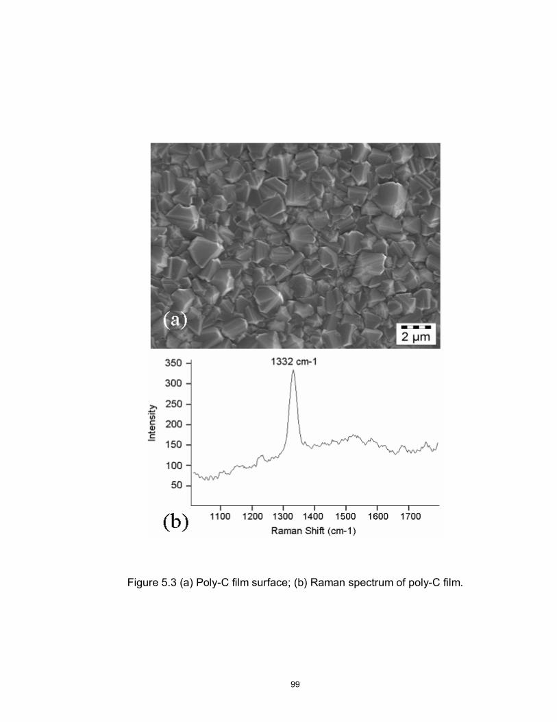
99
Figure 5.3 (a) Poly-C film surface; (b) Raman spectrum of poly-C film.
100
This thin film package fabrication process involves three different steps of
poly-C growth but use the same growth parameters. First, the poly-C
feedthroughs were grown and in-situ doped with TMB diluted in hydrogen
(0.098%). The second poly-C deposition was performed without doping after 4-
µm thick PECVD oxide was deposited and patterned. This layer of poly-C was
patterned to form the first-step package body with access ports. After sacrificial
oxide was removed, final growth of poly-C (5 ~ 6 µm thickness) was performed to
seal the package.
Due to its chemical inertness, it is not possible to pattern poly-C using wet
etching techniques. Several dry etching techniques have been used to effectively
pattern diamond. In this work, a microwave electron-cyclotron-resonance (ECR)
RIE system was used to dry-etch the poly-C film. The ECR systems differ from
other microwave systems in their capability of coupling microwave power to the
plasma at a very low pressure of around 1 mtorr resulting in surface damage-free
processing, high anisotropic etch rate and excellent uniformity.
5.3.2 Poly-C Thin Film Package
Figure 5.4 shows the first generation of fabricated poly-C thin film package,
with size of 1 mm x 1.2 mm. Four large fluidic access ports were opened on this
package, one at each corner. Insets (a) – (c) are close views of package details.
During the sacrificial oxide etching, a diluted HF solution (HF:H2O = 1:3) was
used. A dropper was used repeatedly to blow small bubbles generated by
etching reactions off package chip. The entire package was released in about 6
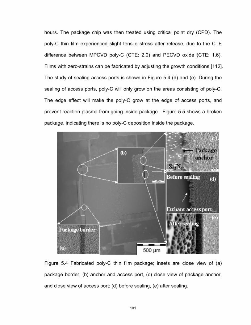
101
hours. The package chip was then treated using critical point dry (CPD). The
poly-C thin film experienced slight tensile stress after release, due to the CTE
difference between MPCVD poly-C (CTE: 2.0) and PECVD oxide (CTE: 1.6).
Films with zero-strains can be fabricated by adjusting the growth conditions [112].
The study of sealing access ports is shown in Figure 5.4 (d) and (e). During the
sealing of access ports, poly-C will only grow on the areas consisting of poly-C.
The edge effect will make the poly-C grow at the edge of access ports, and
prevent reaction plasma from going inside package. Figure 5.5 shows a broken
package, indicating there is no poly-C deposition inside the package.
Figure 5.4 Fabricated poly-C thin film package; insets are close view of (a)
package border, (b) anchor and access port, (c) close view of package anchor,
and close view of access port: (d) before sealing, (e) after sealing.
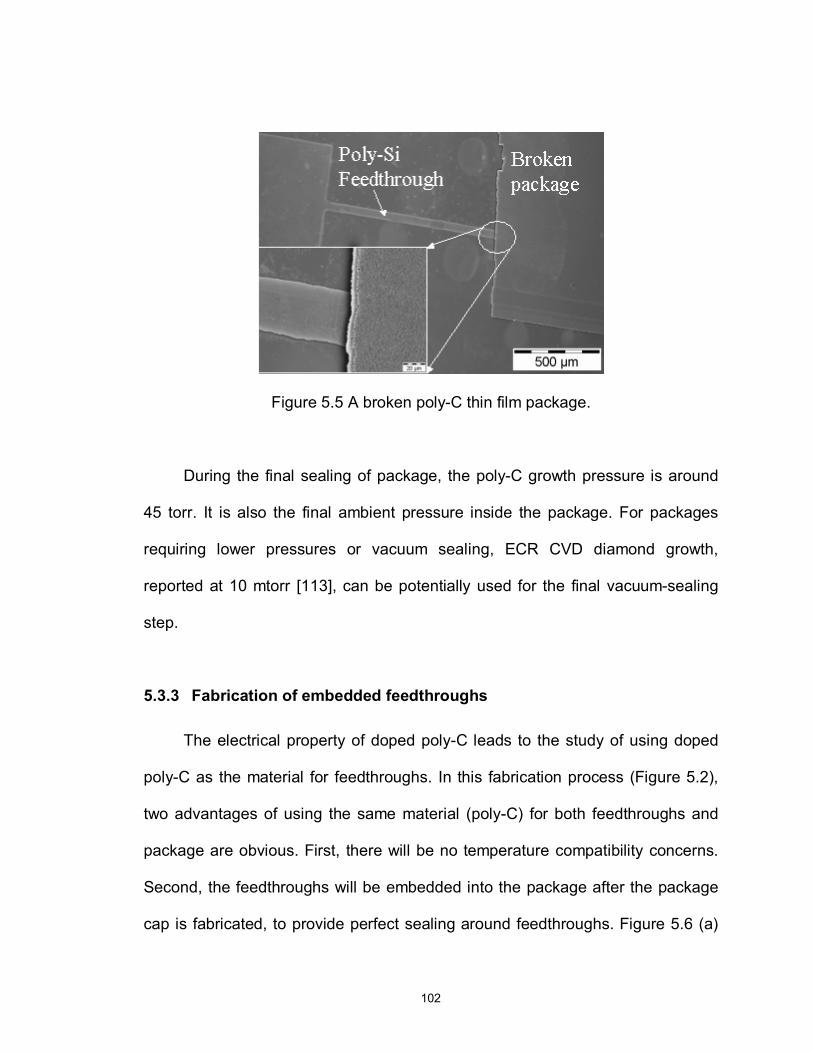
102
Figure 5.5 A broken poly-C thin film package.
During the final sealing of package, the poly-C growth pressure is around
45 torr. It is also the final ambient pressure inside the package. For packages
requiring lower pressures or vacuum sealing, ECR CVD diamond growth,
reported at 10 mtorr [113], can be potentially used for the final vacuum-sealing
step.
5.3.3 Fabrication of embedded feedthroughs
The electrical property of doped poly-C leads to the study of using doped
poly-C as the material for feedthroughs. In this fabrication process (Figure 5.2),
two advantages of using the same material (poly-C) for both feedthroughs and
package are obvious. First, there will be no temperature compatibility concerns.
Second, the feedthroughs will be embedded into the package after the package
cap is fabricated, to provide perfect sealing around feedthroughs. Figure 5.6 (a)
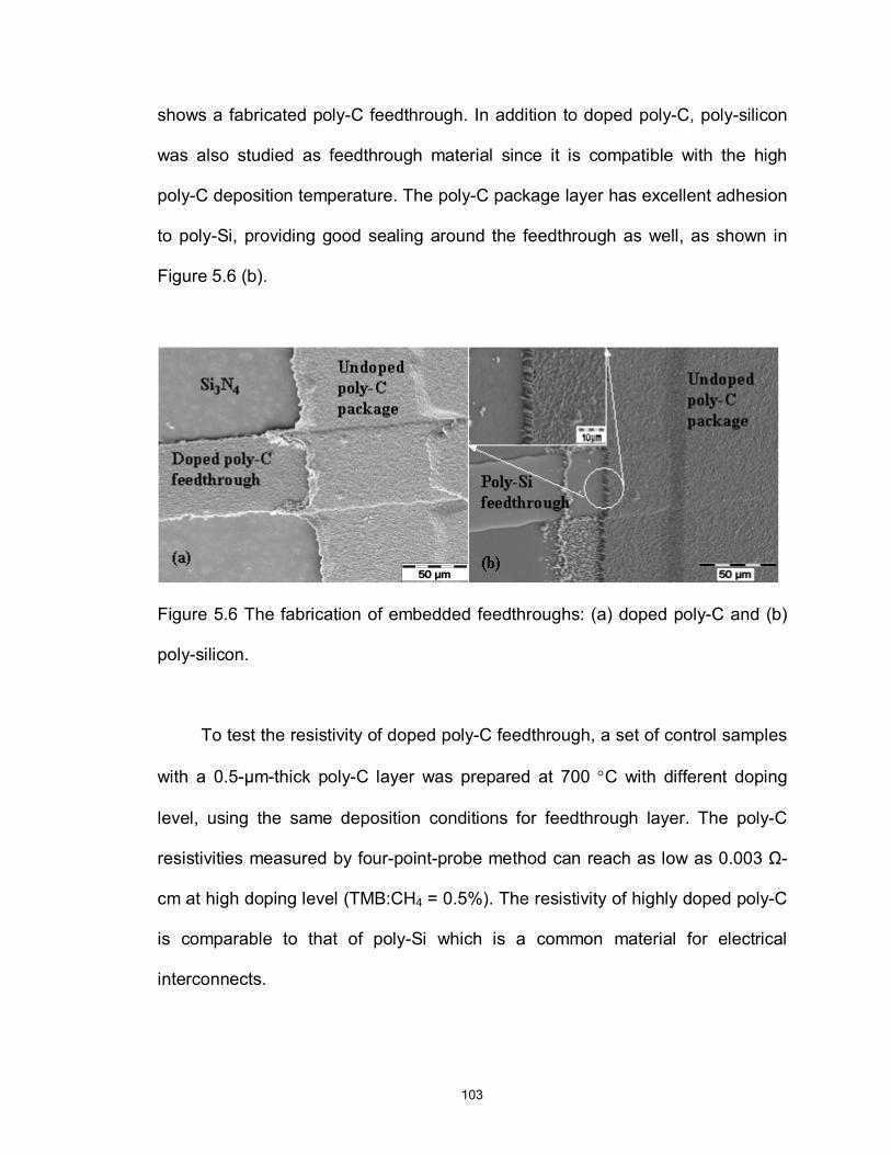
103
shows a fabricated poly-C feedthrough. In addition to doped poly-C, poly-silicon
was also studied as feedthrough material since it is compatible with the high
poly-C deposition temperature. The poly-C package layer has excellent adhesion
to poly-Si, providing good sealing around the feedthrough as well, as shown in
Figure 5.6 (b).
Figure 5.6 The fabrication of embedded feedthroughs: (a) doped poly-C and (b)
poly-silicon.
To test the resistivity of doped poly-C feedthrough, a set of control samples
with a 0.5-µm-thick poly-C layer was prepared at 700 °C with different doping
level, using the same deposition conditions for feedthrough layer. The poly-C
resistivities measured by four-point-probe method can reach as low as 0.003 Ω-
cm at high doping level (TMB:CH4 = 0.5%). The resistivity of highly doped poly-C
is comparable to that of poly-Si which is a common material for electrical
interconnects.
104
5.4 Evaluation of Poly-C Encapsulation Packaging
Technology
This poly-C encapsulation thin film package was developed to provide
MEMS device and even on-chip circuits a package shell for protections from
outside environments. One advantage of this package is the chemical inertness
of poly-C. The corrosion-resistant of poly-C allows this packaging technology to
be used for harsh environmental applications. This encapsulation packaging
process was also designed to fit into post-MEMS fabrication. The additional poly-
C growth for package sealing will require temperature compatibility of MEMS
device. In this section, a long-term corrosion-resistant test of poly-C was
performed. Also, this packaging technology was evaluated by encapsulating
poly-C cantilever beam resonators. Measurements have been taken on pre- and
post-packaging samples using piezoelectric actuation method to explore the
efficacy of poly-C thin film packaging process on sealed resonators.
5.4.1 Corrosion-resistant test of poly-C package
An experiment was designed to test the corrosion-resistant and hermiticity
of poly-C package in severe environment. The 2-mask fabrication process is
shown in Figure 5.7. Starting with bare silicon wafer, a layer of PECVD oxide with
thickness around 4 µm was deposited, as shown Figure 5.8 (a), using the same
deposition parameters as for thin film packaging process. After the oxide layer
was patterned, a layer of poly-C was deposited and patterned using ECR plasma
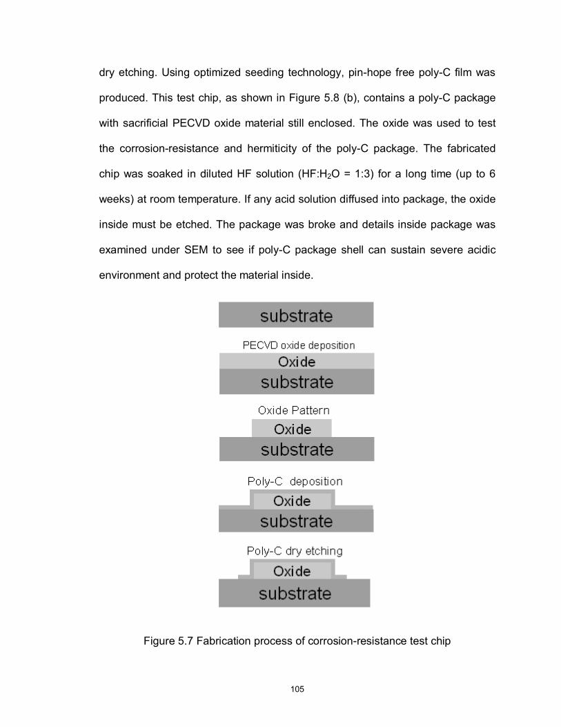
105
dry etching. Using optimized seeding technology, pin-hope free poly-C film was
produced. This test chip, as shown in Figure 5.8 (b), contains a poly-C package
with sacrificial PECVD oxide material still enclosed. The oxide was used to test
the corrosion-resistance and hermiticity of the poly-C package. The fabricated
chip was soaked in diluted HF solution (HF:H2O = 1:3) for a long time (up to 6
weeks) at room temperature. If any acid solution diffused into package, the oxide
inside must be etched. The package was broke and details inside package was
examined under SEM to see if poly-C package shell can sustain severe acidic
environment and protect the material inside.
Figure 5.7 Fabrication process of corrosion-resistance test chip
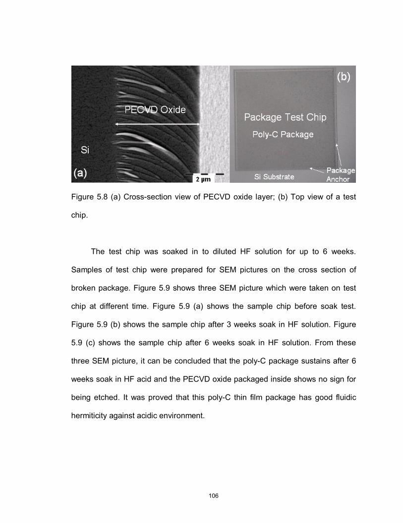
106
Figure 5.8 (a) Cross-section view of PECVD oxide layer; (b) Top view of a test
chip.
The test chip was soaked in to diluted HF solution for up to 6 weeks.
Samples of test chip were prepared for SEM pictures on the cross section of
broken package. Figure 5.9 shows three SEM picture which were taken on test
chip at different time. Figure 5.9 (a) shows the sample chip before soak test.
Figure 5.9 (b) shows the sample chip after 3 weeks soak in HF solution. Figure
5.9 (c) shows the sample chip after 6 weeks soak in HF solution. From these
three SEM picture, it can be concluded that the poly-C package sustains after 6
weeks soak in HF acid and the PECVD oxide packaged inside shows no sign for
being etched. It was proved that this poly-C thin film package has good fluidic
hermiticity against acidic environment.
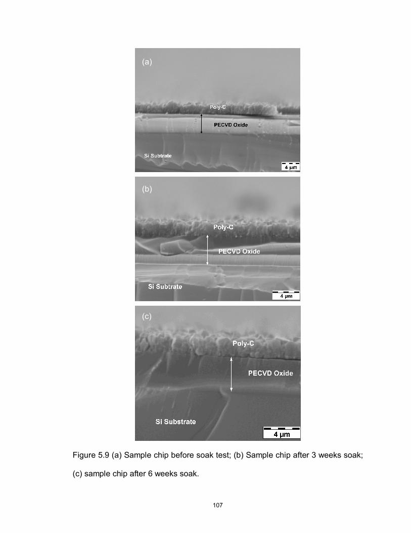
107
Figure 5.9 (a) Sample chip before soak test; (b) Sample chip after 3 weeks soak;
(c) sample chip after 6 weeks soak.
(a)
(b)
(c)
108
5.4.2 Poly-C encapsulation package for cantilever resonator
The additional poly-C growth for package sealing will require temperature
compatibility of MEMS device. One way to evaluate this packaging technology is
to package an actual MEMS device. Taking advantage of the poly-C resonator
study in our group [114], poly-C cantilever beam resonator structure was
selected to be packaged and tested. Testing of resonator was jointly done with
Nelson Sepulveda using Sandia National Lab’s facilities. Measurements have
been taken on pre- and post-packaging samples using piezoelectric actuation
and laser detection method to explore the efficacy of poly-C thin film packaging
process on sealed resonators.
5.4.2.1 Piezoelectric actuation and laser detection for resonator
measurement
The concept of piezoelectric actuation method is to physically attach the
sample that contains the resonator structure to a piezo transducer. This piezo
element is driven by the output of a spectrum analyzer. For the laser detection, a
laser beam is focused on the resonating structure. The laser is reflected off the
point of the resonator structure where the amplitude of motion is maximum (the
tip of the cantilever) and directed to a photodiode. The reflected signal is used to
determine the frequency of vibration. A schematic of the piezoelectric actuation
and detection set up is shown in Figure 5.10.
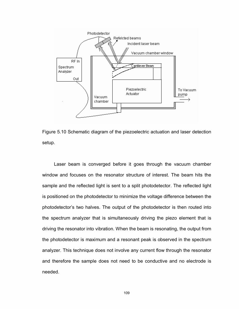
109
Figure 5.10 Schematic diagram of the piezoelectric actuation and laser detection
setup.
Laser beam is converged before it goes through the vacuum chamber
window and focuses on the resonator structure of interest. The beam hits the
sample and the reflected light is sent to a split photodetector. The reflected light
is positioned on the photodetector to minimize the voltage difference between the
photodetector’s two halves. The output of the photodetector is then routed into
the spectrum analyzer that is simultaneously driving the piezo element that is
driving the resonator into vibration. When the beam is resonating, the output from
the photodetector is maximum and a resonant peak is observed in the spectrum
analyzer. This technique does not involve any current flow through the resonator
and therefore the sample does not need to be conductive and no electrode is
needed.
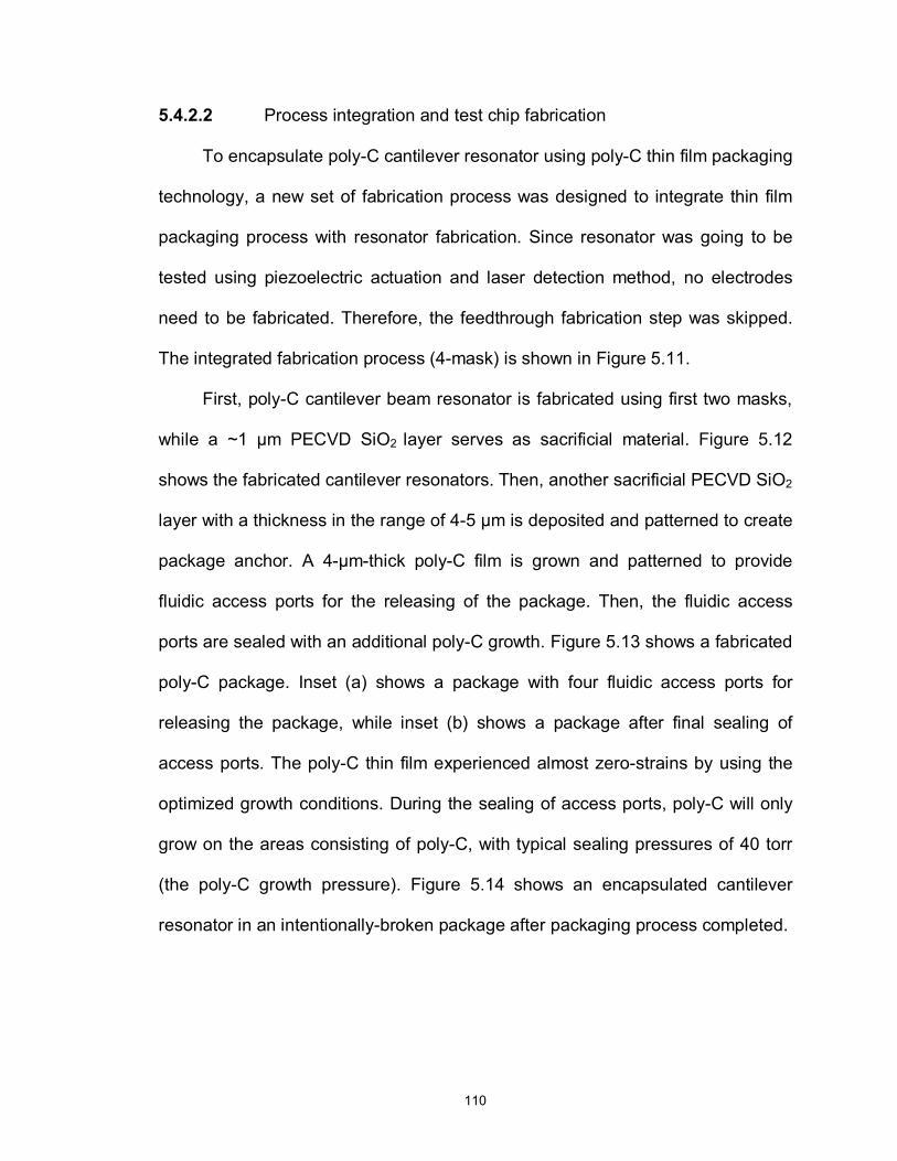
110
5.4.2.2 Process integration and test chip fabrication
To encapsulate poly-C cantilever resonator using poly-C thin film packaging
technology, a new set of fabrication process was designed to integrate thin film
packaging process with resonator fabrication. Since resonator was going to be
tested using piezoelectric actuation and laser detection method, no electrodes
need to be fabricated. Therefore, the feedthrough fabrication step was skipped.
The integrated fabrication process (4-mask) is shown in Figure 5.11.
First, poly-C cantilever beam resonator is fabricated using first two masks,
while a ~1 µm PECVD SiO2 layer serves as sacrificial material. Figure 5.12
shows the fabricated cantilever resonators. Then, another sacrificial PECVD SiO2
layer with a thickness in the range of 4-5 µm is deposited and patterned to create
package anchor. A 4-µm-thick poly-C film is grown and patterned to provide
fluidic access ports for the releasing of the package. Then, the fluidic access
ports are sealed with an additional poly-C growth. Figure 5.13 shows a fabricated
poly-C package. Inset (a) shows a package with four fluidic access ports for
releasing the package, while inset (b) shows a package after final sealing of
access ports. The poly-C thin film experienced almost zero-strains by using the
optimized growth conditions. During the sealing of access ports, poly-C will only
grow on the areas consisting of poly-C, with typical sealing pressures of 40 torr
(the poly-C growth pressure). Figure 5.14 shows an encapsulated cantilever
resonator in an intentionally-broken package after packaging process completed.
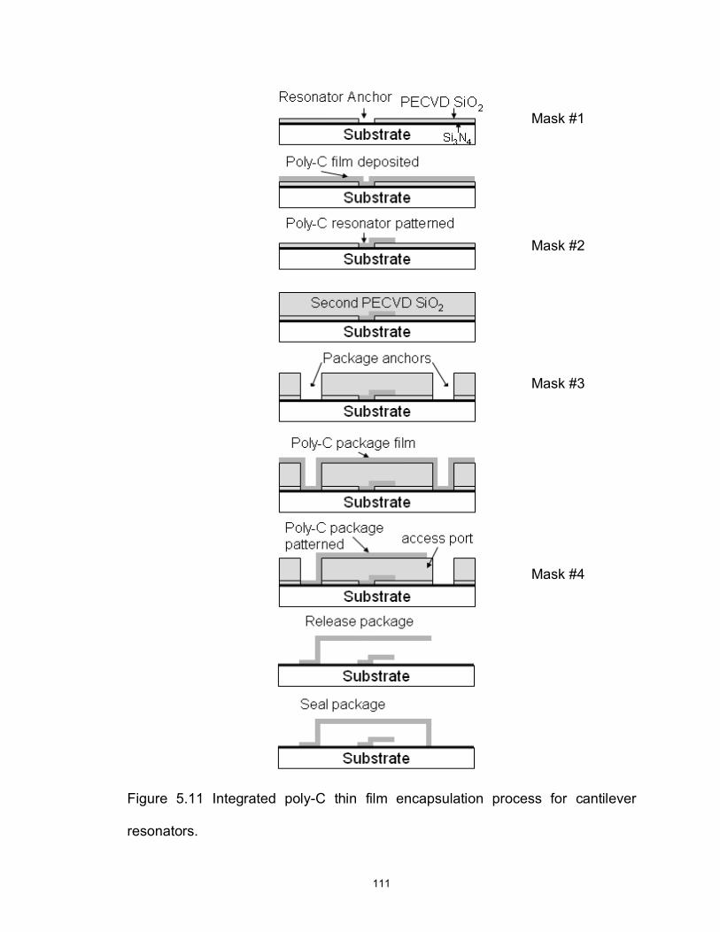
111
Figure 5.11 Integrated poly-C thin film encapsulation process for cantilever
resonators.
Mask #1
Mask #2
Mask #3
Mask #4
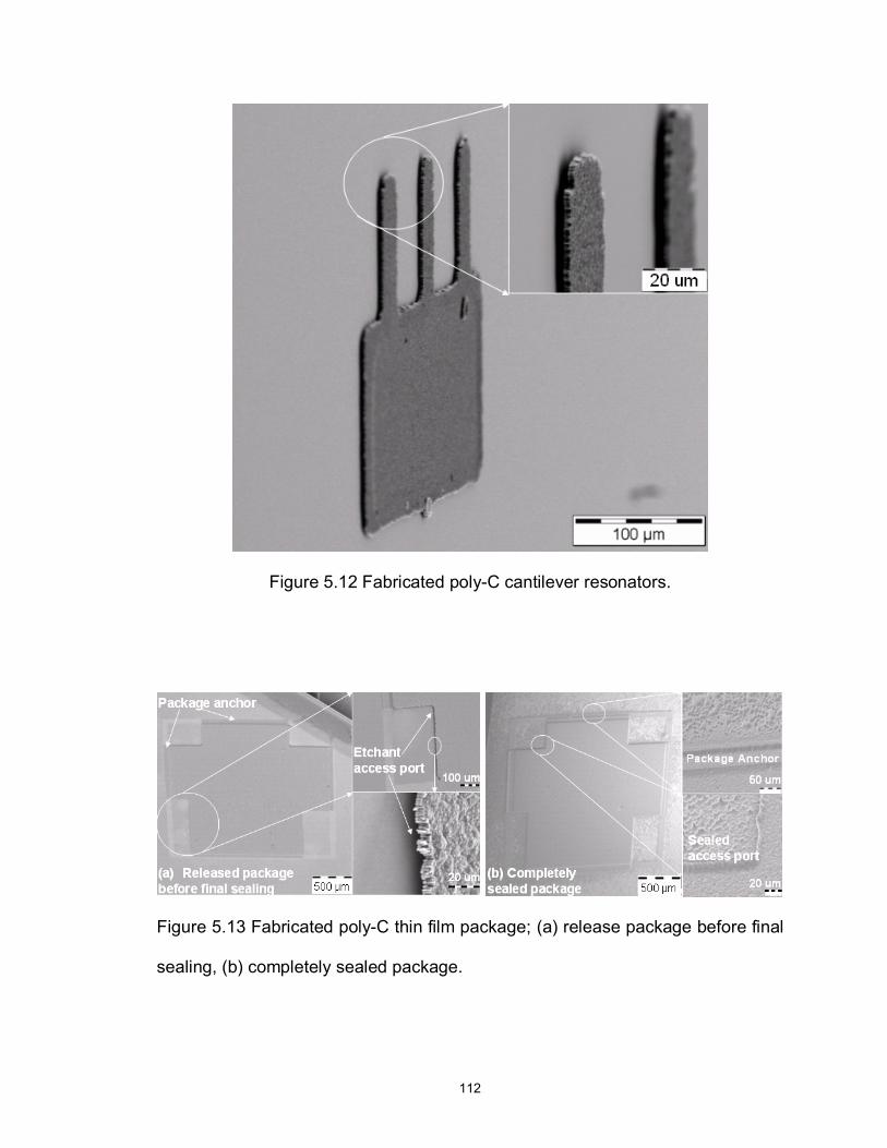
112
Figure 5.12 Fabricated poly-C cantilever resonators.
Figure 5.13 Fabricated poly-C thin film package; (a) release package before final
sealing, (b) completely sealed package.
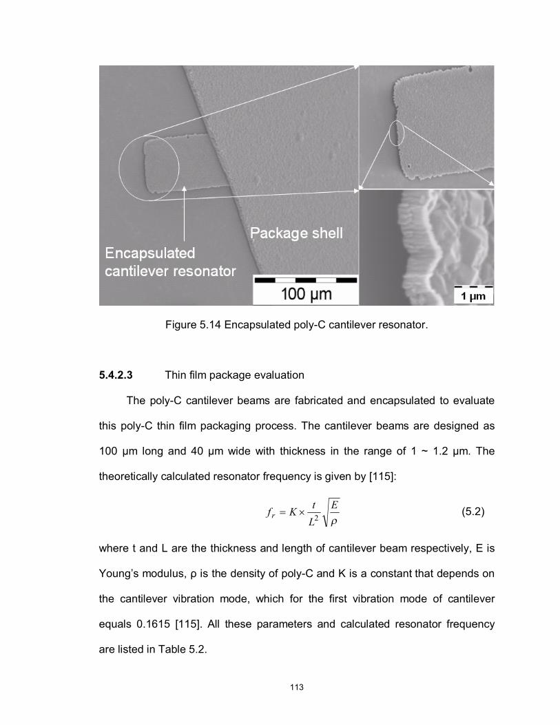
113
Figure 5.14 Encapsulated poly-C cantilever resonator.
5.4.2.3 Thin film package evaluation
The poly-C cantilever beams are fabricated and encapsulated to evaluate
this poly-C thin film packaging process. The cantilever beams are designed as
100 µm long and 40 µm wide with thickness in the range of 1 ~ 1.2 μm. The
theoretically calculated resonator frequency is given by [115]:
ρE
LtKf r 2×= (5.2)
where t and L are the thickness and length of cantilever beam respectively, E is
Young’s modulus, ρ is the density of poly-C and K is a constant that depends on
the cantilever vibration mode, which for the first vibration mode of cantilever
equals 0.1615 [115]. All these parameters and calculated resonator frequency
are listed in Table 5.2.
114
Since the piezoelectric actuation method needs to shine a laser directly on
top of the beam, the package shell was broken for SEM and measurement. For
some samples, the package shell was broken during packaging process right
after package release but before the final sealing of access ports. Figure 5.15
shows cantilever beams (a) before packaging and (b) after packaging, and
corresponding frequency spectrum measurement results. Measured resonator
frequency and quality factor are also highlighted in Table 5.2.
The measured resonator frequencies are only slightly shifted as compared
to the computed values. It may be due to the fact that the actual value of Young’s
modulus of poly-C film is lower than the value of 1000 GPa, which is used for
theoretical calculation. Measured Q value is in the range of 3500 ~ 4500. There
are many mechanisms that cause Q degradation in poly-C resonators [114].
These include point or linear defects within the material and grain sliding or
internal friction. Researchers have also found a dependence of Q on the surface
roughness of the resonator structure [116]. Therefore, the Q values obtained for
different poly-C resonators can vary from structure to structure depending on the
processing and characterization of the films from which the structures were made.
The resonant frequency and quality factor of cantilever beams do not show
appreciable change between pre- and post-packaging measurements. This
indicates that the poly-C thin film packaging process developed in this study does
not affect the yields of resonators packaged inside.
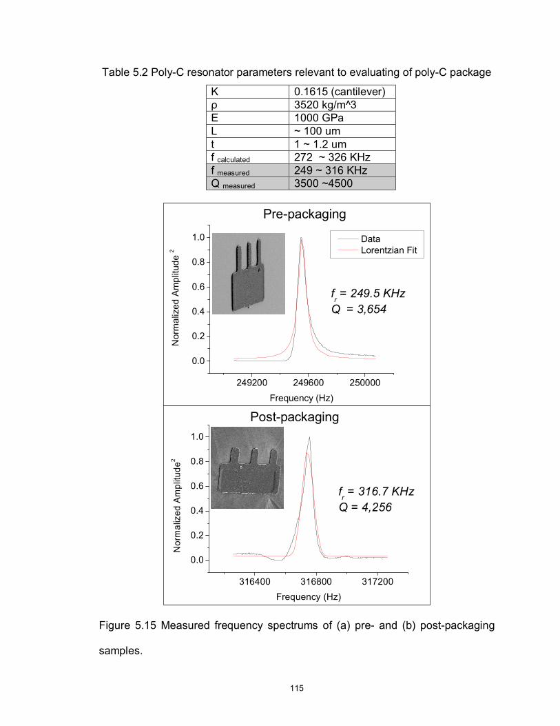
115
Table 5.2 Poly-C resonator parameters relevant to evaluating of poly-C package
K 0.1615 (cantilever) ρ 3520 kg/m^3 E 1000 GPa L ~ 100 um t 1 ~ 1.2 um f calculated 272 ~ 326 KHz f measured 249 ~ 316 KHz Q measured 3500 ~4500
249200 249600 250000
0.0
0.2
0.4
0.6
0.8
1.0
Nor
mal
ized
Am
plitu
de 2
Frequency (Hz)
Data Lorentzian Fit
fr = 249.5 KHzQ = 3,654
316400 316800 317200
0.0
0.2
0.4
0.6
0.8
1.0
fr = 316.7 KHzQ = 4,256
Nor
mal
ized
Am
plitu
de2
Frequency (Hz)
Pre-packaging
Post-packaging
Figure 5.15 Measured frequency spectrums of (a) pre- and (b) post-packaging
samples.
116
Chapter 6
Conclusion and Future Research
6.1 Summary and Conclusions
1. Fundamental research on CVD poly-C technology
Fundamental poly-C technologies used in this study, such as seeding,
deposition, doping and patterning have been investigated. Experimental
parameters have been characterized and optimized. This research provides solid
foundation for enabling technology development and package design and
fabrication later.
2. Enabling technology development
Intensive study has been conducted to develop several enabling poly-C
MEMS technologies, such as freestanding poly-C MEMS structure fabrication,
ultra-fast growth model, packaging panel with built-in interconnects and initial
diamond-diamond bonding investigation. These enabling technologies ensure
applications of poly-C in MEMS packaging at system level.
3. Poly-C thin film encapsulation packaging process
Design, fabrication and evaluation of poly-C thin film encapsulation
packaging process have been studied. To evaluate the efficacy of poly-C
117
encapsulation, poly-C cantilever beam resonators were tested using piezoelectric
actuation and laser detection method before and after poly-C packaging process.
This poly-C thin film packaging process was reported for the first time.
6.2 Future Research Topics
As a long term research project, this PhD study has great continuity for
future student who is willing to work on diamond MEMS packaging. Possible
research topics from this study include:
1. In-depth study on diamond-diamond CVD bonding technology.
With introduction of access holes, CVD bonding between two films
can be greatly improved. This technology, along with thick poly-C
panel fabrication technology using ultra-fast growth model, may
lead to potential applications of building 3-D poly-C cubic package.
2. Further study on poly-C panel with built-in interconnects. This topic
reveals an all-diamond packaging concept. Future research may
focus on the applications of such concept/technology.
3. Improve poly-C encapsulation packaging process. For example,
instead of sealing the package under typical diamond growth
pressure, try to explore potential vacuum sealing method.
4. Based on the development of diamond-diamond bonding
technology, it is possible to fabricate a poly-C MEMS using wafer
bonding approaches.

118
APPENDICES
119
APPENDIX A
Procedure of DPR Preparation
1. Weigh 800 mg commercially available diamond powder
2. Heat the diamond powder in a clean beaker on hot plate for ~ 1hour.
3. Cool powder for ~ 10 minutes
4. add 30 ml thinner into beaker
5. Magnetic stirring for 10 minutes
6. Ultrasonication for 30 minutes
7. add 80 ml photoresist
8. Repeat step 5 and 6
9. Ready to use
Note:
1. Step 2 is needed to eliminate moisture. Also fracture the diamond clusters if
any.
2. Steps for mix thinner with diamond powder (4 – 6) are optional.
3. Mixing ratio is adjustable
4. Do NOT use chemicals which are expired.
120
APPENDIX B
Procedure of Diamond-loaded Isopropanol Alcohol (IPA) Preparation
1. Weigh 7000 mg commercially available diamond powder
2. Heat the diamond powder in a clean beaker on hot plate for ~ 1hour.
3. Cool powder for ~ 10 minutes or longer
4. add 1400 ml IPA into beaker
5. Magnetic stirring for 10 minutes
6. Ultrasonication for 30 minutes
7. Ready to use.
Note:
1. Step 2 is needed to eliminate moisture. Also fracture the diamond clusters if
any.
2. Mixing ratio is adjustable
3. Do NOT use chemicals which are expired.
121
APPENDIX C
The Operation Procedure of MPCVD
(For diamond and CNT deposition)
1. Check if main chamber is in vacuum or not. If it is, then:
a) Close the valve of vacuum pump
b) Vent system with Nitrogen gas
c) Turn off valve of venting gas
2. Load the sample on substrate holder, then lift substrate holder stage up to the
resonant cavity, drive two screws to fix the stage.
ATTENTION: Do it with gloves if chamber is hot!!!
3. Close the main chamber door, open the vacuum valve.
4. Wait for system pressure drops to below 3 mtorr.
5. Turn on cooling water and gas, push the “off” red button in the panel of
WAVEMAT.
6. Turn on Microwave power (at bottom)
7. Turn on valves of H2 and CH4 gas cylinders.
8. On H2 channel, pre-set H2 gas flow rate to 100 sccm.
9. Set pressure “A” (2.5 torr) in MKS, turn on H2 channel.
10. Wait for pressure to be stable at 2.5 torr, turn on Microwave
11. You must see plasma formed in the cavity. If not, adjust the resonant cavity
length.
12. Set desired deposition pressure (i.e. 40 torr). After pressure goes up to 10 torr,

122
increase microwave power slowly to desired value/
Optional: increase H2 flow rate to introduce gas faster.
13. When pressure approaches to set value, set H2 flow rate back to 100 sccm.
14. When pressure reaches set value, check reflected power, adjust to reduce it
as low as possible.
15. On CH4 channel, pre-set CH4 gas flow rate to 1.5 sccm or value you want.
Turn on CH4 channel.
16. Deposition process starts.
Shut down procedure:
17. Turn off CH4 channel, wait for 5 minutes.
18. Decrease pressure to 2.5 torr, and microwave power to 0.6 kW slowly.
19. Turn off microwave power, turn off H2 channel.
20. Turn on vacuum valve.
21. Cool system for more than half hour.
22. Close vacuum valve, vent system with N2.
23. Open chamber door and take out sample.
24. Close chamber door.
25. Close all gas cylinder valves.
26. Turn off microwave power.

123
BIBLIGRAPHY
124
BIBLIGRAPHY
[1] J. Giesler, G. Omalley, G. Omalley, M. Williams, and S. Machuga, "Flip-Chip on Board Connection Technology - Process Characterization and Reliability," Ieee Transactions on Components Packaging and Manufacturing Technology Part B-Advanced Packaging, vol. 17, pp. 256-263, 1994.
[2] D. Suryanarayana, T. Y. Wu, and J. A. Varcoe, "Encapsulants Used in Flip-Chip Packages," Ieee Transactions on Components Hybrids and Manufacturing Technology, vol. 16, pp. 858-862, 1993.
[3] J. Kloeser, E. Zakel, F. Bechtold, and H. Reichl, "Reliability investigations of fluxless flip-chip interconnections on green tape ceramic substrates," Ieee Transactions on Components Packaging and Manufacturing Technology Part A, vol. 19, pp. 24-33, 1996.
[4] L. W. Lin, "MEMS Packaging at the Wafer Level," Journal of Materials Processing and Manufacturing Science, vol. 8, pp. 347-349, 2000.
[5] K. Ikeda, H. Kuwayama, T. Kobayashi, T. Watanabe, T. Nishikawa, T. Yoshida, and K. Harada, "Silicon Pressure Sensor Integrates Resonant Strain-Gauge on Diaphragm," Sensors and Actuators a-Physical, vol. 21, pp. 146-150, 1990.
[6] L. W. Lin, R. T. Howe, and A. P. Pisano, "Microelectromechanical filters for signal processing," Journal of Microelectromechanical Systems, vol. 7, pp. 286-294, 1998.
[7] B. Ziaie, J. A. VonArx, M. R. Dokmeci, and K. Najafi, "A hermetic glass-silicon micropackage with high-density on-chip feedthroughs for sensors and actuators," Journal of Microelectromechanical Systems, vol. 5, pp. 166-179, 1996.
[8] L. W. Lin, "MEMS post-packaging by localized heating and bonding," Ieee Transactions on Advanced Packaging, vol. 23, pp. 608-616, 2000.
[9] J. T. Butler, V. M. Bright, and J. H. Comtois, "Multichip module packaging of microelectromechanical systems," Sensors and Actuators a-Physical, vol. 70, pp. 15-22, 1998.
[10] J. T. Butler, V. M. Bright, and R. J. Saia, "Investigation of MEMS packaging using multichip module foundries," Sensors and Materials, vol. 11, pp. 87-104, 1999.
125
[11] A. Ucok, J. Giachino, and K. Najafi, "Compact, Modular Assembly and Packaging of Multi-Substrates Microsystems," presented at IEEE 12th Int. Conf. on Solid-state Sensors, Actuators and Microsystems, Boston, MA, pp. 1877-1878,2003.
[12] H. Bjorkman, P. Rangsten, U. Simu, J. Karlsson, P. Hollman, and K. Hjort, "Diamond Microstructure Replicas From Silicon Masters," presented at IEEE Int. Conference on MEMS, Germany, pp. 24-29,1998.
[13] H. Bjorkman, P. Rangsten, P. Hollman, and K. Hjort, "Diamond replicas from microstructured silicon masters," Sensors and Actuators a-Physical, vol. 73, pp. 24-29, 1999.
[14] M. Aslam and D. Schulz, "Technology of Diamond MicroElectroMechanical Systems," presented at IEEE 8th Int. Conf. on Solid State Sensors, Actuators and Microsystems (Transducers '95), Stockholm, Sweden, pp. 222-224,1995.
[15] E. Kohn, P. Gluche, and M. Adamschik, "Diamond MEMS - a new emerging technology," Diamond and Related Materials, vol. 8, pp. 934-940, 1999.
[16] N. Sepulveda-Alancastro and D. M. Aslam, "Polycrystalline diamond technology for RFMEMS resonators," Microelectronic Engineering, vol. 73-74, pp. 435-440, 2004.
[17] K. A. Moores and Y. K. Joshi, "High Performance Packaging Materials for Improved Thermal Management of Power Electronics," Future Circuits International, vol. 7, pp. 45-49, 2001.
[18] X. W. Zhu, D. M. Aslam, Y. X. Tang, B. H. Stark, and K. Najafi, "The fabrication of all-diamond packaging panels with built-in interconnects for wireless integrated microsystems," Journal of Microelectromechanical Systems, vol. 13, pp. 396-405, 2004.
[19] T. R. Hsu, MEMS and Microsystems - Design and Manufacture. Boston: McGraw-Hill, 2002.
[20] S. D. Senturia, Microsystem Design. Nowell. MA: Kluwer Academic Pulishers, 2001.
[21] J. Y. Chen, L. S. Huang, C. H. Chu, and C. Peizen, "A new transferred ultra-thin silicon micropackaging," Journal of Micromechanics and Microengineering, vol. 12, pp. 406-409, 2002.
[22] A. Hochst, R. Scheuerer, H. Stahl, F. Fischer, L. Metzger, R. Reichenbach, F. Larmer, S. Kronmuller, S. Watcham, C. Rusu, A. Witvrouw, and R. Gunn, "Stable thin film encapsulation of acceleration sensors using
126
polycrystalline silicon as sacrificial and encapsulation layer," Sensors and Actuators a-Physical, vol. 114, pp. 355-361, 2004.
[23] Y. S. Choi, J. S. Park, H. D. Park, Y. H. Song, J. S. Jung, and S. G. Kang, "Effects of temperatures on microstructures and bonding strengths of Si-Si bonding using bisbenzocyclobutene," Sensors and Actuators a-Physical, vol. 108, pp. 201-205, 2003.
[24] R. de Reus, C. Christensen, S. Weichel, S. Bouwstra, J. Janting, G. F. Eriksen, K. Dyrbye, T. R. Brown, J. P. Krog, O. S. Jensen, and P. Gravesen, "Reliability of industrial packaging for microsystems," Microelectronics Reliability, vol. 38, pp. 1251-1260, 1998.
[25] J. T. Huang and H. A. Yang, "Improvement of bonding time and quality of anodic bonding using the spiral arrangement of multiple point electrodes," Sensors and Actuators a-Physical, vol. 102, pp. 1-5, 2002.
[26] C. Lee, W. F. Huang, and J. S. Shie, "Wafer bonding by low-temperature soldering," Sensors and Actuators a-Physical, vol. 85, pp. 330-334, 2000.
[27] P. Lindner, V. Dragoi, S. Farrens, T. Glinsner, and P. Hangweier, "Advanced techniques for 3D devices in wafer-bonding processes," Solid State Technology, vol. 47, pp. 55, 2004.
[28] M. A. Schmidt, "Wafer-to-wafer bonding for microstructure formation," Proceedings of the IEEE Transactions on Advanced Packaging, vol. 86, pp. 1575-1585, 1998.
[29] T. J. Harpster and K. Najafi, "Long-Term Testing of hermetic Anodically Bonded Glass-Silicon Packages," presented at IEEE Int. Conference on MEMS, Las Vegas, NV, pp.,2002.
[30] T. J. Harpster, S. Hauvespre, M. R. Dokmeci, and K. Najafi, "A passive humidity monitoring system for in situ remote wireless testing of micropackages," Journal of Microelectromechanical Systems, vol. 11, pp. 61-67, 2002.
[31] H. Henmi, S. Shoji, Y. Shoji, K. Yoshimi, and M. Esashi, "Vacuum Packaging for Microsensors by Glass Silicon Anodic Bonding," Sensors and Actuators a-Physical, vol. 43, pp. 243-248, 1994.
[32] B. Lee, S. Seok, and K. Chun, "A study on wafer level vacuum packaging for MEMS devices," Journal of Micromechanics and Microengineering, vol. 13, pp. 663-669, 2003.
[33] K. Birkelund, P. Gravesen, S. Shiryaev, P. B. Rasmussen, and M. D. Rasmussen, "High-pressure silicon sensor with low-cost packaging," Sensors and Actuators a-Physical, vol. 92, pp. 16-22, 2001.
127
[34] A. P. London, A. A. Ayon, A. H. Epstein, S. M. Spearing, T. Harrison, Y. Peles, and J. L. Kerrebrock, "Microfabrication of a high pressure bipropellant rocket engine," Sensors and Actuators a-Physical, vol. 92, pp. 351-357, 2001.
[35] Y. T. Cheng, L. W. Lin, and K. Najafi, "Localized silicon fusion and eutectic bonding for MEMS fabrication and packaging," Journal of Microelectromechanical Systems, vol. 9, pp. 3-8, 2000.
[36] M. N. Nguyen and M. B. Grosse, "Low Moisture Polymer Adhesive for Hermetic Packages," Ieee Transactions on Components Hybrids and Manufacturing Technology, vol. 15, pp. 964-971, 1992.
[37] E. T. Enikov and J. G. Boyd, "Electroplated electro-fluidic interconnects for chemical sensors," Sensors and Actuators a-Physical, vol. 84, pp. 161-164, 2000.
[38] R. Bartek, J. A. Foerster, and R. F. Wolffenbuttel, "Vacuum sealing of microcavities using metal evaporation," Sensors and Actuators a-Physical, vol. 61, pp. 364-368, 1997.
[39] B. H. Stark and K. Najafi, "A low-temperature thin-film electroplated metal vacuum package," Journal of Microelectromechanical Systems, vol. 13, pp. 147-157, 2004.
[40] R. Fillion, R. Wojnarowski, B. Gorowitz, W. Daum, and H. Cole, "Conformal multichip-on-flex (MCM-F) technology," presented at International Conference on Multichip | Modules (SPIE vol. 2575), pp.,1995.
[41] D. A. Doane, Multichip module technologies and alternatives: the basics, vol. ch1 pp. 3-11. New York: Van Nostrand Reinhold, 1993.
[42] R. Agarwal and M. Pecht, Physical architecture of VLSI systems, vol. ch. 6, pp. 351-386. New York: Wiley, 1994.
[43] S. F. Al-Sarawi, D. Abbott, and P. D. Franzon, "A review of 3-D packaging technology," Ieee Transactions on Components Packaging and Manufacturing Technology Part B-Advanced Packaging, vol. 21, pp. 2-14, 1998.
[44] R. Crowley, "Three-dimenstional electronics packaging," TechSearch International, Inc., 9430 Research Blvd., Building 4 Suite 400, Austin, Texas 78759, Tech. Rep. Nov. 1993 1993.
[45] S. Ladd, "Designing 3D multichip modules for high volume applications-three case studies," presented at International Conference and Exhibition. Multichip Modules (SPIE Proc. vol.1986), Denver, CO, pp. 417-421,1993.
128
[46] M. Schuenemann et al., "MEMS Modular Packaging and Interfaces," presented at IEEE Electronic Components and Technology Conference, pp. 681-688,2000.
[47] A. B. Ucok, J. M. Giachino, and K. Najafi, "Modular Assembly/Packaging of Multi-Substrate Microsystems (WIMS Cube) Using Thermo-Magnetically Actuated Cables," presented at 18th IEEE International Conference on Micro Electro Mechanical Systems (MEMS '05), Miami Beach, FL, pp. 536-539,2005.
[48] W. Hanke, G. Strinati, and H. J. Mattaush, "Dynamical correlation effects on the one-electron states of covalent crystals," presented at Int. Conf. Europ. Phys. Soc., pp.,1980.
[49] Spear and Dismukes, Synthetic Diamond - Emerging CVD Science and Technology. New York: Wiley, 1994.
[50] A. Lettington and J. W. Steeds, Thin Film Diamond, 1st ed. London, UK: Chapman & Hall, 1994.
[51] P. W. May, M. N. R. Ashfold, K. N. Rosser, N. M. Everitt, and C. G. Trevor, "Diamond Deposition in a Hot Filament Reactor Using Different Hydrocarbon Precursor Gases," Appllied Surface Science, vol. 68, pp. 299-305, 1993.
[52] P. W. May, C. A. Rego, R. M. Thomas, M. N. R. Ashfold, K. N. Rosser, and N. M. Everitt, "CVD Diamond Wires and Tubes," Diamond and Related Materials, vol. 3, pp. 810-813, 1994.
[53] H. S. Shin and D. G. Goodwin, "Diamond Growth in Premixed Propylene-Oxygen Flames," Applied Physics Letters, vol. 66, pp. 2909-2911, 1995.
[54] K. L. Yarina, D. S. Dandy, E. Jensen, and J. E. Butler, "Growth of diamond films using an enclosed methyl-acetylene and propadiene combustion flame," Diamond and Related Materials, vol. 7, pp. 1491-1502, 1998.
[55] V. I. Konov, A. A. Smolin, V. G. Ralchenko, S. M. Pimenov, E. D. Obraztsova, E. N. Loubnin, G. Sepold, and S. M. Metev, "D.c. arc plasma deposition of smooth nanocrystalline diamond films," Diamond and Related Materials, vol. 4, pp. 1073-1078, 1995.
[56] J. M. Trombetta, J. T. Hoggins, P. Klocek, and T. A. McKenna, "Optical properties of DC arc-discharge plasma CVD diamond," presented at Diamond Optics IV (SPIE), San Diego, CA, USA, pp. 77-88,1991.
[57] P. W. May, M. N. R. Ashfold, K. N. Rosser, and N. M. Everitt, "CVD Diamond Films Produced in a Parallel-Plate RF Reactor," presented at 3rd Int. Symp. Diamond Mater., Honolulu, Hawaii,, pp. 448-454,1993.
129
[58] A. M. Bonnot, B. S. Mathis, J. Mercier, J. Leroy, and J. P. Vitton, "Growth mechanisms of diamond crystals and films prepared by chemical vapor deposition," Diamond and Related Materials, vol. 1, pp. 230-234, 1992.
[59] M. G. Jubber, J. I. B. WilsonI, C. Drummond, P. John, and D. K. Milne, "Microwave plasma chemical vapour deposition of high purity diamond films," Diamond and Related Materials, vol. 2, pp. 402-406, 1993.
[60] V. G. Ralchenko, A. A. Smolin, V. I. Konov, K. F. Sergeichev, I. A. Sychov, I. I. Vlasov, V. V. Migulin, S. V. Voronina, and A. V. Khomich, "Large-area diamond deposition by microwave plasma," Diamond and Related Materials, vol. 6, pp. 417-421, 1997.
[61] T.-H. Chein and Y. Tzeng, "CVD diamond grown by microwave plasma in mixtures of acetone/oxygen and acetone/carbon dioxide," Diamond and Related Materials, vol. 8, pp. 1393-1401, 1999.
[62] A. Badzian, B. L. Weiss, R. Roy, T. Badzian, W. Drawl, P. Mistry, and M. C. Turchan, "Characterization and Electron Field Emission From Diamond Coatings Deposited by Multiply Laser Process," Diamond and Related Materials, vol. 7, pp. 64-69, 1998.
[63] A. R. Badzian, R. Roy, T. Badzian, W. R. Drawl, P. Mistry, and M. C. Turchan, "Application of electron field emission from diamond grown by a multiple pulsed laser process." United States, 2001, pp. 183.
[64] H. Bjorkman, P. Rangsten, and K. Hjort, "Diamond microstructures for optical micro electromechanical systems," Sensors and Actuators a-Physical, vol. 78, pp. 41-47, 1999.
[65] G. S. Sandhu and W. K. Chu, "Reactive Ion Etching of Diamond," Applied Physics Letters, vol. 55, pp. 437-438, 1989.
[66] N. N. Efremow, M. W. Geis, D. C. Flanders, G. A. Lincoln, and N. P. Economou, "Ion-Beam-Assisted Etching of Diamond," Journal of Vacuum Science & Technology B, vol. 3, pp. 416-418, 1985.
[67] H. W. Choi, E. Gu, C. Liu, C. Griffin, J. M. Girkin, I. M. Watson, and M. D. Dawson, "Fabrication of natural diamond microlenses by plasma etching," Journal of Vacuum Science & Technology B, vol. 23, pp. 130-132, 2005.
[68] S. A. Grot, R. A. Ditizio, G. S. Gildenblat, A. R. Badzian, and S. J. Fonash, "Oxygen Based Electron-Cyclotron Resonance Etching of Semiconducting Homoepitaxial Diamond Films," Applied Physics Letters, vol. 61, pp. 2326-2328, 1992.
[69] W. J. Zhang, C. Sun, I. Bello, C. S. Lee, and S. T. Lee, "Bias-assisted etching of polycrystalline diamond films in hydrogen, oxygen, and argon
130
microwave plasmas," Journal of Vacuum Science & Technology a-Vacuum Surfaces and Films, vol. 17, pp. 763-767, 1999.
[70] D. R. Wur, J. L. Davidson, W. P. Kang, and D. L. Kinser, "Polycrystalline Diamond Pressure Sensor," IEEE Journal of Microelectromechanical Systems, vol. 4, pp. 34-41, 1995.
[71] J. Wang, J. E. Butler, T. Feygelson, and C. T.-C. Nguyen, "1.51-GHz Nanocrystalline Diamond Micromechanical Disk Resonator with Material-mismatched Isolating Support," presented at 17th Int. IEEE Micro Electro Mechanical Systems Conf., Maastricht, Netherlands, pp.,2004.
[72] K. Sienski, R. Eden, and D. Schaefer, "3-D electronic interconnect packaging," presented at IEEE Aerospace Applications Conference, Aspen, CO, USA, pp. 363-373,1996.
[73] Y. Namba, E. Heidarpour, and M. Nakayama, "Size Effects Appearing in the Raman-Spectra of Polycrystalline Diamonds," Journal of Applied Physics, vol. 72, pp. 1748-1751, 1992.
[74] R. Saito, T. Takeya, T. Kimura, G. Dresselhaus, and M. S. Dresselhaus, "Finite-size effect on the Raman spectra of carbon nanotubes," Physical Review B, vol. 59, pp. 2388-2392, 1999.
[75] J. B. Bindell, "Scanning Electron Microscopy," in Encyclopedia of Materials Characterization. Boston: Butterworth-Heinemann, 1992.
[76] R. S. Howland and M. D. Kirk, "Scanning Tunneling Microscopy and Scanning Force Microscopy," in Encyclopedia of materials characterization. Boston: Butterworth-Heinemann, 1995.
[77] R. Erz, W. Dotter, K. Jung, and H. Ehrhardt, "Preparation of Smooth and Nanocrystalline Diamond Films," Diamond and Related Materials, vol. 2, pp. 449-453, 1993.
[78] Y. Hayashi, W. Drawl, R. W. Collins, and R. Messier, "In-Process Ellipsometric Monitoring of Diamond Film Growth by Microwave Plasma Enhanced Chemical Vapor-Deposition," Applied Physics Letters, vol. 60, pp. 2868-2870, 1992.
[79] J. S. Ma, H. Kawarada, T. Yonehara, J. Suzuki, J. Wei, Y. Yokota, and A. Hiraki, "Selective Nucleation and Growth of Diamond Particles by Plasma-Assisted Chemical Vapor-Deposition," Applied Physics Letters, vol. 55, pp. 1071-1073, 1989.
[80] J. S. Ma, H. Kawarada, T. Yonehara, J. Suzuki, J. Wei, Y. Yokota, H. Mori, H. Fujita, and A. Hiraki, "Interfacial Structures and Selective Growth of
131
Diamond Particles Formed by Plasma-Assisted Cvd," Applied Surface Science, vol. 41-2, pp. 572-579, 1989.
[81] M. P. Everson and M. A. Tamor, "Studies of Nucleation and Growth-Morphology of Boron-Doped Diamond Microcrystals by Scanning Tunneling Microscopy," Journal of Vacuum Science & Technology B, vol. 9, pp. 1570-1576, 1991.
[82] B. W. Sheldon, R. Csencsits, J. Rankin, R. E. Boekenhauer, and Y. Shigesato, "Bias-Enhanced Nucleation of Diamond During Microwave-Assisted Chemical-Vapor-Deposition," Journal of Applied Physics, vol. 75, pp. 5001-5008, 1994.
[83] F. S. Lauten, Y. Shigesato, and B. W. Sheldon, "Diamond Nucleation on Unscratched Sio2 Substrates," Applied Physics Letters, vol. 65, pp. 210-212, 1994.
[84] B. R. Stoner, G. H. M. Ma, S. D. Wolter, and J. T. Glass, "Characterization of Bias-Enhanced Nucleation of Diamond on Silicon by Invacuo Surface-Analysis and Transmission Electron-Microscopy," Physical Review B, vol. 45, pp. 11067-11084, 1992.
[85] M. Deguchi, M. Kitabatake, H. Kurokawa, T. Shiratori, and M. Kitagawa, "Growth of CVD diamond films on substrates seeded with nano-crystalline diamond particles," Diamond Films and Technology, vol. 7, pp. 273-276, 1997.
[86] D. Lee and R. K. Singh, "Synthesis of (111) oriented diamond thin films by electrophoretic deposition process," Applied Physics Letters, vol. 70, pp. 1542, 1997.
[87] E. Maillard-Schaller, O. M. Kuettel, L. Diederich, L. Schlapbach, V. V. Zhirnov, and P. I. Belobrov, "Surface properties of nanodiamond films deposited by electrophoresis on Si(100)," Diamond and Related Materials, vol. 8, pp. 805-808, 1999.
[88] Y. X. Tang and D. M. Aslam, "Technology of polycrystalline diamond thin films for microsystems applications," Journal of Vacuum Science & Technology B, vol. 23, pp. 1088-1095, 2005.
[89] S. Guillaudeu, X. Zhu, and D. M. Aslam, "Fabrication of 2-mu m wide poly-crystalline diamond channels using silicon molds for micro-fluidic applications," Diamond and Related Materials, vol. 12, pp. 65-69, 2003.
[90] R. E. Shroder, R. J. Nemanich, and J. T. Glass, "Analysis of the composite structures in diamond thin films by Raman spectroscopy," Physical Review B, vol. 41, pp. 3738-3745, 1990.

132
[91] M. E. Baginski, T. A. Baginski, and J. L. Davidson, "Characterization of the Ion-Implantation and Thermal Annealing of Boron in (100) Diamond," Journal of the Electrochemical Society, vol. 137, pp. 2984-2987, 1990.
[92] W. Tsai, M. Delfino, D. Hodul, M. Riaziat, L. Y. Ching, G. Reynolds, and C. B. Cooper, "Diamond MESFET Using Ultrashallow RTP Boron Doping," Ieee Electron Device Letters, vol. 12, pp. 157-159, 1991.
[93] J. F. Prins, "Activation of boron-dopant atoms in ion-implanted diamonds," Physical Review B, vol. 38, pp. 5576-5584, 1988.
[94] Y. Show, T. Matsukawa, H. Ito, M. Iwase, and T. Izumi, "Structural changes in CVD diamond film by boron and nitrogen doping," Diamond and Related Materials, vol. 9, pp. 337-340, 2000.
[95] X. Jiang, P. Willich, M. Paul, and C. P. Klages, "In situ boron doping of chemical-vapor-deposited diamond films," Journal of Materials Research, vol. 14, pp. 3211-3220, 1999.
[96] K. Miyata, K. Kumagai, K. Nishimura, and K. Kobashi, "Morphology of Heavily B-Doped Diamond Films," Journal of Materials Research, vol. 8, pp. 2845-2857, 1993.
[97] J. Cifre, J. Puigdollers, M. C. Polo, and J. Esteve, "Trimethylboron Doping of CVD Diamond Thin-Films," Diamond and Related Materials, vol. 3, pp. 628-631, 1994.
[98] A. Masood, M. Aslam, M. A. Tamor, and T. J. Potter, "Synthesis and Electrical Characterization of Boron-Doped Thin Diamond Films," Applied Physics Letters, vol. 61, pp. 1832-1834, 1992.
[99] K. Hirabayashi, Y. Taniguchi, O. Takamatsu, T. Ikeda, K. Ikoma, and N. Iwasakikurihara, "Selective Deposition of Diamond Crystals by Chemical Vapor-Deposition Using a Tungsten-Filament Method," Applied Physics Letters, vol. 53, pp. 1815-1817, 1988.
[100] T. Roppel, R. Ramesham, C. Ellis, and S. Y. Kee, "Thin film diamond microstructures," in Thin Solid Films, vol. 212, 1992, pp. 56.
[101] J. L. Valdes, J. W. Mitchel, Mucha, and L. Seibles, "Selected-Area Nucleation and Patterning of Diamond Thin Films by Electrophoretic Seeding," Journal of Electrochem. Soc., vol. 138, pp. 635, 1991.
[102] A. Masood, M. Aslam, M. A. Tamor, and T. J. Potter, "Synthesis and electrical characterization of boron-doped thin diamond films," Applied Physics Letter, vol. 61, pp. 1832, 1992.
133
[103] E. Snidero, D. Tromson, C. Mer, P. Bergonzo, J. S. Foord, C. Nebel, O. A. Williams, and R. B. Jackman, "Influence of the postplasma process conditions on the surface conductivity of hydrogenated diamond surfaces," Journal of Applied Physics, vol. 93, pp. 2700-2704, 2003.
[104] P. D. Gigl, "The Strength of Polycrystalline Diamond Compacts," in High Pressure Science and Technology, vol. 1, K. D. Timmerhaus and M. S. Barber, Eds. New York: Plenum, 1979, pp. 914-922.
[105] D. Maier-Schneider, J. Maibach, and E. Obermeier, "A New Analytical Solution for the Load-Deflection of Square Membranes," Journal of Microelectromechanical Systems, vol. 4, pp. 238-241, 1995.
[106] Q. Sun and M. Alam, "Thermal-Oxidation Characteristics of Chemical Vapor-Deposited Diamond Films," Journal of Materials Science, vol. 27, pp. 5857-5862, 1992.
[107] V. G. Ralchenko, T. V. Kononenko, T. Foursova, E. N. Loubnin, V. E. Strelnitsky, J. Seth, and S. V. Babu, "Comparison of Laser and O-2 Plasma-Etching of Diamond-Like Carbon-Films," Diamond and Related Materials, vol. 2, pp. 211-217, 1993.
[108] V. G. Ralchenko, T. V. Kononenko, S. M. Pimenov, N. V. Chernenko, E. N. Loubnin, V. Y. Armeyev, and A. Y. Zlobin, "Catalytic Interaction of Fe, Ni and Pt with Diamond Films - Patterning Applications," Diamond and Related Materials, vol. 2, pp. 904-909, 1993.
[109] A. B. Harker, J. Flintoff, and J. F. DeNatale, "The Polishing of Polycrystalline Diamond Films," Diamond Optics III, SPIE, vol. 1325, pp. 222-229, 1990.
[110] M. Yoshikawa, "Development and Performence of A Diamond Film Polishing Appratus With Hot Metals," Diamond Optics III, SPIE, vol. 1325, pp. 210-217, 1990.
[111] X. Zhu, S. Guillaudeu, D. M. Aslam, U. Kim, B. H. Stark, and K. Najafi, "All Diamond Packaging for Wireless Integrated Micro-Systems Using Ultra-Fast Diamond Growth," presented at IEEE 2003 Int. Conference on MEMS, Kyoto Japan, pp. 658-661,2003.
[112] I. I. Taher, "CVD diamond piezoresistive microsensors," in PhD dissertation. Michigan State University, 1994.
[113] C. R. Eddy, D. L. Youchison, B. D. Sartwell, and K. S. Grabowski, "Deposition of Diamond onto Aluminum by Electron-Cyclotron Resonance Microwave Plasma-Assisted Cvd," Journal of Materials Research, vol. 7, pp. 3255-3259, 1992.
134
[114] N. Sepulveda-Alancastro, D. M. Aslam, and J. P. Sullivan, "Polycrystalline Diamond MEMS Resonator Technology for Sensor Applications," Diamond and Related Materials, vol. In Press, 2005.
[115] W. Weaver, S. P. Timoshenko, and D. H. Young, Vibration Problems in Engineering, 5th ed: Wiley Publishers, 1990.
[116] P. Mohanty, D. A. Harrington, K. L. Ekinci, Y. T. Yang, M. J. Murphy, and M. L. Roukes, "Intrinsic dissipation in high-frequency micromechanical resonators," Physical Review B, vol. 66, pp. -, 2002.


![1-benzyl-15,3,5,7-tetraazatricyclo [3.3.1.1~3,7~]decane](https://img.pdfslide.net/doc/110x75/56813095550346895d967216/1-benzyl-15357-tetraazatricyclo-331137decane.jpg)
