Embed Size (px)
Citation preview
Differential/Single-Ended Input, Dual 1 MSPS, 12-Bit, 3-Channel SAR ADC
Data Sheet AD7265
Rev. C Document Feedback Information furnished by Analog Devices is believed to be accurate and reliable. However, no responsibility is assumed by Analog Devices for its use, nor for any infringements of patents or other rights of third parties that may result from its use. Specifications subject to change without notice. No license is granted by implication or otherwise under any patent or patent rights of Analog Devices. Trademarks and registered trademarks are the property of their respective owners.
One Technology Way, P.O. Box 9106, Norwood, MA 02062-9106, U.S.A. Tel: 781.329.4700 ©2005–2018 Analog Devices, Inc. All rights reserved. Technical Support www.analog.com
FEATURES Dual 12-bit, 3-channel ADC Throughput rate: 1 MSPS Specified for VDD of 2.7 V to 5.25 V Power consumption
7 mW at 1 MSPS with 3 V supplies 17 mW at 1 MSPS with 5 V supplies
Pin-configurable analog inputs 12-channel single-ended inputs 6-channel fully differential inputs 6-channel pseudo differential inputs
70 dB SINAD at 50 kHz input frequency Accurate on-chip reference: 2.5 V
±0.2% maximum at 25°C, 20 ppm/°C maximum Dual conversion with read 875 ns, 16 MHz SCLK High speed serial interface
SPI®-/QSPI™-/MICROWIRE™-/DSP-compatible −40°C to +125°C operation Shutdown mode: 1 µA maximum 32-lead LFCSP and 32-lead TQFP 2 MSPS version, AD7266
GENERAL DESCRIPTION The AD72651 is a dual, 12-bit, high speed, low power, successive approximation ADC that operates from a single 2.7 V to 5.25 V power supply and features throughput rates of up to 1 MSPS. The device contains two ADCs, each preceded by a 3-channel multiplexer, and a low noise, wide bandwidth track-and-hold amplifier that can handle input frequencies in excess of 30 MHz.
The conversion process and data acquisition use standard control inputs allowing easy interfacing to microprocessors or DSPs. The input signal is sampled on the falling edge of CS; conversion is also initiated at this point. The conversion time is determined by the SCLK frequency. The AD7265 uses advanced design techniques to achieve very low power dissipation at high throughput rates. With 5 V supplies and a 1 MSPS throughput rate, the part consumes 4 mA maximum. The part also offers flexible power/throughput rate management when operating in normal mode, because the quiescent current consumption is so low.
The analog input range for the part can be selected to be a 0 V to VREF (or 2 × VREF) range, with either straight binary or twos complement output coding. The AD7265 has an on-chip 2.5 V reference that can be overdriven when an external reference is preferred. This external reference range is 100 mV to VDD. The AD7265 is available in 32-lead LFCSP and 32-lead TQFP.
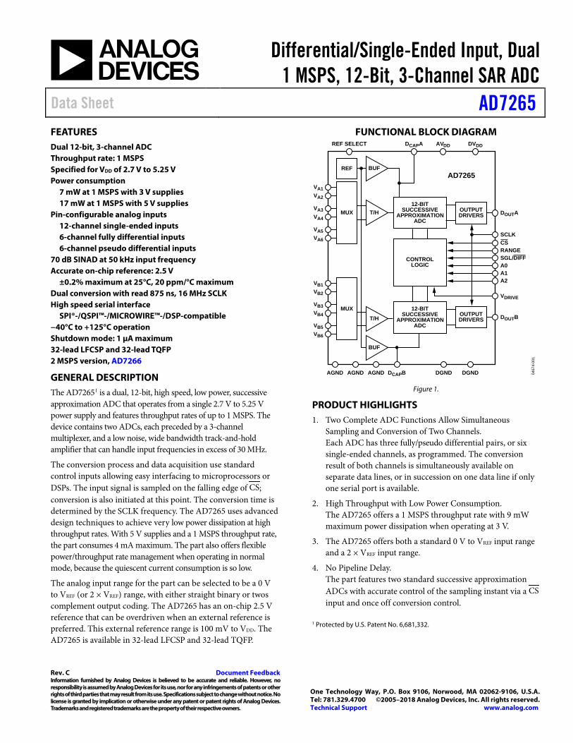
FUNCTIONAL BLOCK DIAGRAM
12-BITSUCCESSIVE
APPROXIMATIONADC
DOUTAOUTPUTDRIVERS
CONTROLLOGIC
T/H
BUF
VA1VA2
VA3VA4
VA5VA6
MUX
REFAD7265
VDRIVE
REF SELECT DCAPA AVDD DVDD
BUF
DOUTBOUTPUTDRIVERS
12-BITSUCCESSIVE
APPROXIMATIONADC
T/H
VB1VB2
VB3VB4
VB5VB6
MUX
AGND AGND AGND DCAPB DGND DGND
CSSCLK
RANGESGL/DIFFA0A1A2
0467
4-00
1
Figure 1.
PRODUCT HIGHLIGHTS 1. Two Complete ADC Functions Allow Simultaneous
Sampling and Conversion of Two Channels. Each ADC has three fully/pseudo differential pairs, or six single-ended channels, as programmed. The conversion result of both channels is simultaneously available on separate data lines, or in succession on one data line if only one serial port is available.
2. High Throughput with Low Power Consumption. The AD7265 offers a 1 MSPS throughput rate with 9 mW maximum power dissipation when operating at 3 V.
3. The AD7265 offers both a standard 0 V to VREF input range and a 2 × VREF input range.
4. No Pipeline Delay. The part features two standard successive approximation ADCs with accurate control of the sampling instant via a CS input and once off conversion control.
1 Protected by U.S. Patent No. 6,681,332.
AD7265 Data Sheet
Rev. C | Page 2 of 27
TABLE OF CONTENTS Features .............................................................................................. 1 General Description ......................................................................... 1 Functional Block Diagram .............................................................. 1 Product Highlights ........................................................................... 1 Revision History ............................................................................... 2 Specifications ..................................................................................... 3
Timing Specifications .................................................................. 5 Absolute Maximum Ratings ............................................................ 6
ESD Caution .................................................................................. 6 Pin Configurations and Function Descriptions ........................... 7 Typical Performance Characteristics ............................................. 9 Terminology .................................................................................... 11 Theory of Operation ...................................................................... 13
Circuit Information .................................................................... 13 Converter Operation .................................................................. 13 Analog Input Structure .............................................................. 13 Analog Inputs .............................................................................. 14 Analog Input Selection .............................................................. 17 Output Coding ............................................................................ 17 Transfer Functions...................................................................... 18
Digital Inputs .............................................................................. 18 VDRIVE ............................................................................................ 18
Modes of Operation ....................................................................... 19 Normal Mode .............................................................................. 19 Partial Power-Down Mode ....................................................... 19 Full Power-Down Mode ............................................................ 20 Power-Up Times ......................................................................... 21 Power vs. Throughput Rate ....................................................... 21
Serial Interface ................................................................................ 22 Microprocessor Interfacing ........................................................... 23
AD7265 to ADSP-2181 .............................................................. 23 AD7265 to ADSP-BF531 ........................................................... 24 AD7265 to TMS320C541 .......................................................... 24 AD7265 to DSP563xx ................................................................ 25
Application Hints ........................................................................... 26 Grounding and Layout .............................................................. 26 PCB Design Guidelines for LFCSP .......................................... 26 Evaluating the AD7265 Performance ...................................... 26
Outline Dimensions ....................................................................... 27 Ordering Guide .......................................................................... 27
REVISION HISTORY 1/2018—Rev. B to Rev. C Changed CP-32-7 to CP-32-2 ...................................... Throughout Changes to Figure 2 .......................................................................... 7 Changed AD7265 to ADSP-218x Section Heading to AD7265 to ADSP-2181 Section Heading ........................................................ 23 Changes to AD7265 to ADSP-2181 Section and Figure 43 ...... 23 Changed AD7265 to ADSP-BF53x Section Heading to AD7265 to ADSP-BF532 Section Heading ................................................. 24 Changes to AD7265 to ADSP-BF532 Section and Figure 44 ... 24 Updated Outline Dimensions ....................................................... 27 Changes to Ordering Guide .......................................................... 27 1/2017—Rev. A to Rev. B Changed CP-32-2 to CP-32-7 ...................................... Throughout Changes to Figure 2 .......................................................................... 7 Updated Outline Dimensions ....................................................... 27 Changes to Ordering Guide .......................................................... 27
11/2006—Rev. 0 to Rev. A Changes to Format ............................................................. Universal Changes to Reference Input/Output Section ................................. 4 Changes to Table 4 ............................................................................. 7 Changes to Terminology Section ................................................. 11 Changes to Figure 24 and Differential Mode Section ............... 15 Changes to Figure 29 ...................................................................... 16 Changes to AD7265 to ADSP-BF53x Section ............................ 24 Updated Outline Dimensions ....................................................... 27 Changes to Ordering Guide .......................................................... 27 4/2005—Revision 0: Initial Version

Data Sheet AD7265
Rev. C | Page 3 of 27
SPECIFICATIONS TA = TMIN to TMAX, VDD = 2.7 V to 5.25 V, fSCLK = 16 MHz, fS = 1 MSPS, VDRIVE = 2.7 V to 5.25 V; specifications apply using internal reference or external reference = 2.5 V ± 1%, unless otherwise noted.1
Table 1. Parameter Specification Unit Test Conditions/Comments DYNAMIC PERFORMANCE
Signal-to-Noise Ratio (SNR)2 71 dB min fIN = 50 kHz sine wave; differential mode 69 dB min fIN = 50 kHz sine wave; single-ended and
pseudo differential modes Signal-to-Noise + Distortion Ratio (SINAD)2 70 dB min fIN = 50 kHz sine wave; differential mode 68 dB min fIN = 50 kHz sine wave; single-ended and
pseudo differential modes Total Harmonic Distortion (THD)2 –77 dB max fIN = 50 kHz sine wave; differential mode –73 dB max fIN = 50 kHz sine wave; single-ended and
pseudo differential modes Spurious-Free Dynamic Range (SFDR)2 –75 dB max fIN = 50 kHz sine wave Intermodulation Distortion (IMD)2 fa = 30 kHz, fb = 50 kHz
Second-Order Terms –88 dB typ Third-Order Terms –88 dB typ
Channel-to-Channel Isolation –88 dB typ SAMPLE AND HOLD
Aperture Delay3 11 ns max Aperture Jitter3 50 ps typ Aperture Delay Matching3 200 ps max Full Power Bandwidth 33/26 MHz typ at 3 dB, VDD = 5 V/VDD = 3 V
3.5/3 MHz typ at 0.1 dB, VDD = 5 V/VDD = 3 V DC ACCURACY
Resolution 12 Bits Integral Nonlinearity2 ±1 LSB max ±0.5 LSB typ; differential mode
±1.5 LSB max ±0.5 LSB typ; single-ended and pseudo differential modes
Differential Nonlinearity2,4 ±0.99 LSB max Differential mode −0.99/+1.5 LSB max Single-ended and pseudo differential modes Straight Binary Output Coding
Offset Error ±6 LSB max Offset Error Match ±2 LSB typ Gain Error ±2.5 LSB max Gain Error Match ±0.5 LSB typ
Twos Complement Output Coding Positive Gain Error ±2 LSB max Positive Gain Error Match ±0.5 LSB typ Zero Code Error ±5 LSB max Zero Code Error Match ±1 LSB typ Negative Gain Error ±2 LSB max Negative Gain Error Match ±0.5 LSB typ
ANALOG INPUT5 Single-Ended Input Range 0 V to VREF V RANGE pin low 0 V to 2 × VREF RANGE pin high Pseudo Differential Input Range: VIN+ − VIN−
6 0 to VREF V RANGE pin low 2 × VREF V RANGE pin high
Fully Differential Input Range: VIN+ and VIN− VCM ± VREF/2 V VCM = common-mode voltage7 = VREF/2 VIN+ and VIN− VCM ± VREF V VCM = VREF
AD7265 Data Sheet
Rev. C | Page 4 of 27
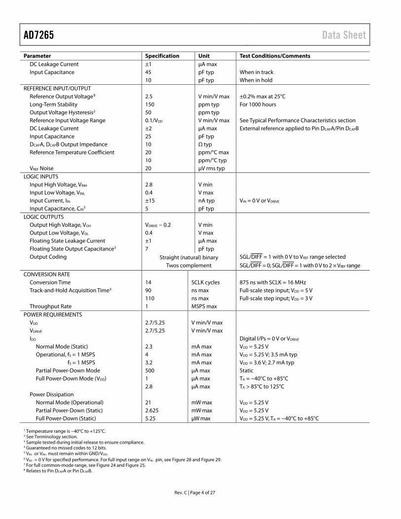
Parameter Specification Unit Test Conditions/Comments DC Leakage Current ±1 µA max Input Capacitance 45 pF typ When in track
10 pF typ When in hold REFERENCE INPUT/OUTPUT
Reference Output Voltage8 2.5 V min/V max ±0.2% max at 25°C Long-Term Stability 150 ppm typ For 1000 hours Output Voltage Hysteresis2 50 ppm typ Reference Input Voltage Range 0.1/VDD V min/V max See Typical Performance Characteristics section DC Leakage Current ±2 µA max External reference applied to Pin DCAPA/Pin DCAPB Input Capacitance 25 pF typ DCAPA, DCAPB Output Impedance 10 Ω typ Reference Temperature Coefficient 20 ppm/°C max 10 ppm/°C typ VREF Noise 20 µV rms typ
LOGIC INPUTS Input High Voltage, VINH 2.8 V min Input Low Voltage, VINL 0.4 V max Input Current, IIN ±15 nA typ VIN = 0 V or VDRIVE Input Capacitance, CIN
3 5 pF typ LOGIC OUTPUTS
Output High Voltage, VOH VDRIVE − 0.2 V min Output Low Voltage, VOL 0.4 V max Floating State Leakage Current ±1 µA max Floating State Output Capacitance3 7 pF typ Output Coding Straight (natural) binary SGL/DIFF = 1 with 0 V to VREF range selected
Twos complement SGL/DIFF = 0; SGL/DIFF = 1 with 0 V to 2 × VREF range
CONVERSION RATE Conversion Time 14 SCLK cycles 875 ns with SCLK = 16 MHz Track-and-Hold Acquisition Time3 90 ns max Full-scale step input; VDD = 5 V 110 ns max Full-scale step input; VDD = 3 V Throughput Rate 1 MSPS max
POWER REQUIREMENTS VDD 2.7/5.25 V min/V max VDRIVE 2.7/5.25 V min/V max IDD
Digital I/Ps = 0 V or VDRIVE Normal Mode (Static) 2.3 mA max VDD = 5.25 V Operational, fS = 1 MSPS 4 mA max VDD = 5.25 V; 3.5 mA typ
fS = 1 MSPS 3.2 mA max VDD = 3.6 V; 2.7 mA typ Partial Power-Down Mode 500 µA max Static Full Power-Down Mode (VDD) 1 µA max TA = −40°C to +85°C 2.8 µA max TA > 85°C to 125°C
Power Dissipation Normal Mode (Operational) 21 mW max VDD = 5.25 V Partial Power-Down (Static) 2.625 mW max VDD = 5.25 V Full Power-Down (Static) 5.25 µW max VDD = 5.25 V, TA = −40°C to +85°C
1 Temperature range is −40°C to +125°C. 2 See Terminology section. 3 Sample tested during initial release to ensure compliance. 4 Guaranteed no missed codes to 12 bits. 5 VIN− or VIN+ must remain within GND/VDD. 6 VIN− = 0 V for specified performance. For full input range on VIN− pin, see Figure 28 and Figure 29. 7 For full common-mode range, see Figure 24 and Figure 25. 8 Relates to Pin DCAPA or Pin DCAPB.

Data Sheet AD7265
Rev. C | Page 5 of 27
TIMING SPECIFICATIONS AVDD = DVDD = 2.7 V to 5.25 V, VDRIVE = 2.7 V to 5.25 V, internal/external reference = 2.5 V, TA = TMAX to TMIN, unless otherwise noted1.
Table 2. Parameter Limit at TMIN, TMAX Unit Description fSCLK
2 1 MHz min TA = −40°C to +85°C 4 MHz min TA > 85°C to 125°C 16 MHz max tCONVERT 14 × tSCLK ns max tSCLK = 1/fSCLK 875 ns max fSCLK = 16 MHz tQUIET 30 ns min Minimum time between end of serial read and next falling edge of CS t2 15/20 ns min VDD = 5 V/3 V, CS to SCLK setup time, TA = −40°C to +85°C
20/30 ns min VDD = 5 V/3 V, CS to SCLK setup time, TA > 85°C to 125°C
t3 15 ns max Delay from CS until DOUTA and DOUTB are three-state disabled
t43
36 ns max Data access time after SCLK falling edge, VDD = 3 V 27 ns max Data access time after SCLK falling edge, VDD = 5 V t5 0.45 tSCLK ns min SCLK low pulse width t6 0.45 tSCLK ns min SCLK high pulse width t7 10 ns min SCLK to data valid hold time, VDD = 3 V 5 ns min SCLK to data valid hold time, VDD = 5 V t8 15 ns max CS rising edge to DOUTA, DOUTB, high impedance
t9 30 ns min CS rising edge to falling edge pulse width
t10 5 ns min SCLK falling edge to DOUTA, DOUTB, high impedance 50 ns max SCLK falling edge to DOUTA, DOUTB, high impedance 1 Sample tested during initial release to ensure compliance. All input signals are specified with tr = tf = 5 ns (10% to 90% of VDD) and timed from a voltage level of 1.6 V.
All timing specifications given are with a 25 pF load capacitance. With a load capacitance greater than this value, a digital buffer or latch must be used. See the Serial Interface section and Figure 41 and Figure 42.
2 Minimum SCLK for specified performance; with slower SCLK frequencies, performance specifications apply typically. 3 The time required for the output to cross 0.4 V or 2.4 V.
AD7265 Data Sheet
Rev. C | Page 6 of 27
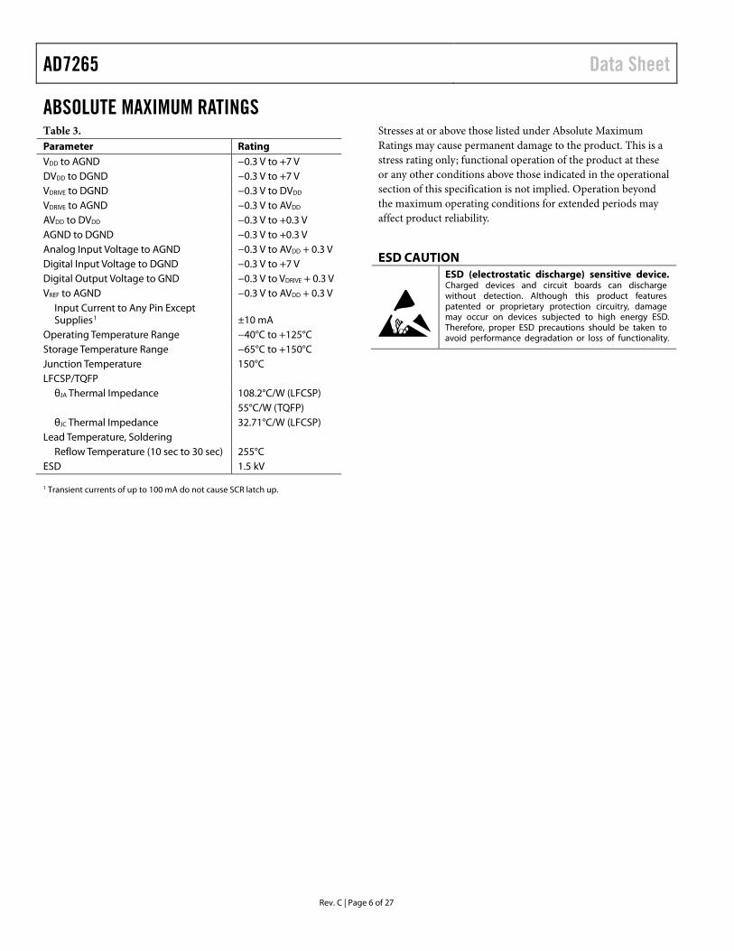
ABSOLUTE MAXIMUM RATINGS Table 3. Parameter Rating VDD to AGND −0.3 V to +7 V DVDD to DGND −0.3 V to +7 V VDRIVE to DGND −0.3 V to DVDD VDRIVE to AGND −0.3 V to AVDD AVDD to DVDD −0.3 V to +0.3 V AGND to DGND −0.3 V to +0.3 V Analog Input Voltage to AGND −0.3 V to AVDD + 0.3 V Digital Input Voltage to DGND −0.3 V to +7 V Digital Output Voltage to GND −0.3 V to VDRIVE + 0.3 V VREF to AGND −0.3 V to AVDD + 0.3 V
Input Current to Any Pin Except Supplies1 ±10 mA
Operating Temperature Range −40°C to +125°C Storage Temperature Range −65°C to +150°C Junction Temperature 150°C LFCSP/TQFP
θJA Thermal Impedance 108.2°C/W (LFCSP) 55°C/W (TQFP) θJC Thermal Impedance 32.71°C/W (LFCSP)
Lead Temperature, Soldering Reflow Temperature (10 sec to 30 sec) 255°C
ESD 1.5 kV 1 Transient currents of up to 100 mA do not cause SCR latch up.
Stresses at or above those listed under Absolute Maximum Ratings may cause permanent damage to the product. This is a stress rating only; functional operation of the product at these or any other conditions above those indicated in the operational section of this specification is not implied. Operation beyond the maximum operating conditions for extended periods may affect product reliability.
ESD CAUTION
Data Sheet AD7265
Rev. C | Page 7 of 27
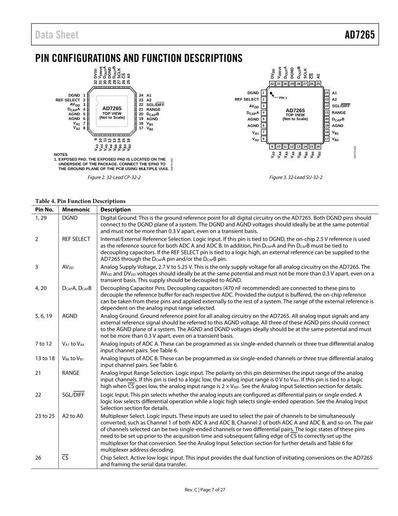
PIN CONFIGURATIONS AND FUNCTION DESCRIPTIONS
0467
4-00
2
12345678
2423222120191817
9 10 11 12 13 14 15 16
32 31 30 29 28 27 26 25
AD7265TOP VIEW
(Not to Scale)
A1A2SGL/DIFFRANGEDCAPBAGNDVB1VB2
DGNDREF SELECT
AVDDDCAPAAGNDAGND
VA1VA2
V A3
V A4
V A5
V A6
V B6
V B5
V B4
V B3
DVD
DV D
RIV
ED
OU
TAD
GN
DD
OU
TBSC
LKC
SA
0
NOTES1. EXPOSED PAD. THE EXPOSED PAD IS LOCATED ON THE UNDERSIDE OF THE PACKAGE. CONNECT THE EPAD TO THE GROUND PLANE OF THE PCB USING MULTIPLE VIAS.
Figure 2. 32-Lead CP-32-2
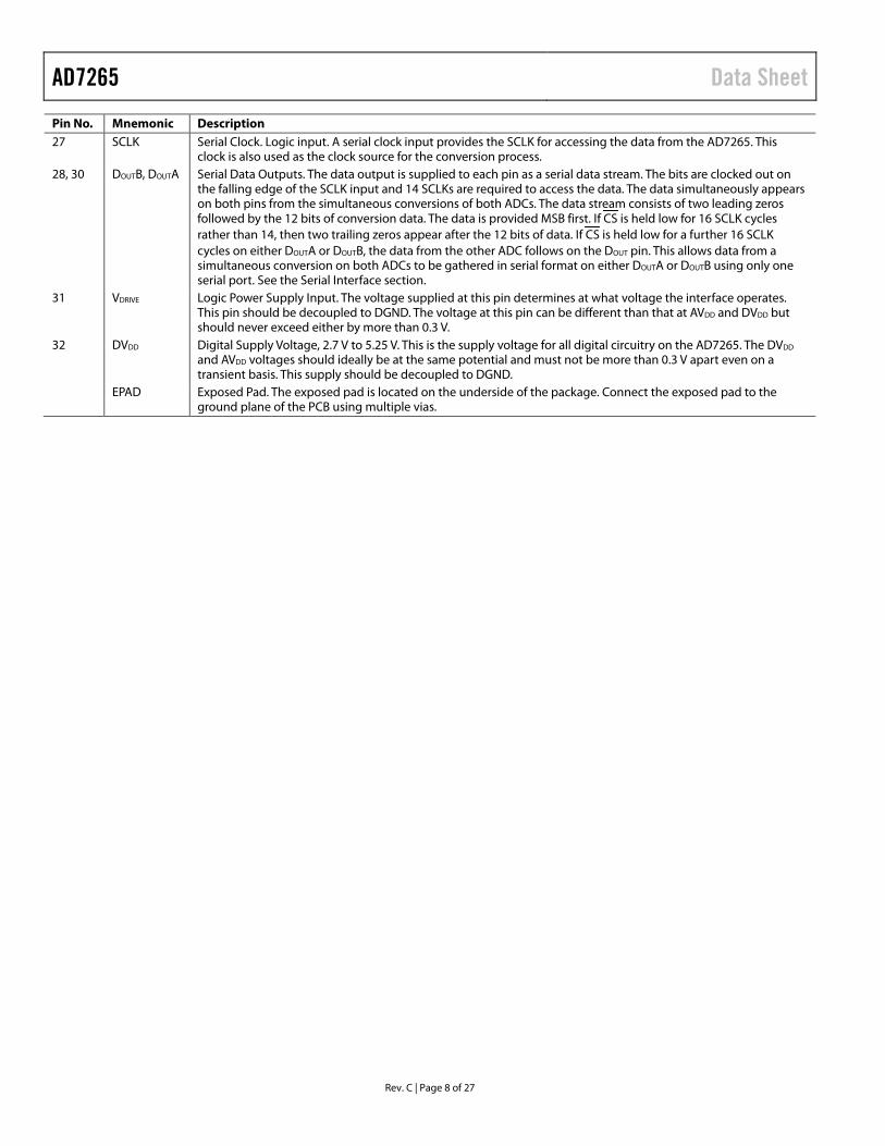
0467
4-04
1
CS
SGL/DIFF
1
2
3
4
5
6
7
8
REF SELECTAVDD
DCAPA
VA1
AGNDAGND
DGND
VA2
23 A222
21 RANGE
18 VB1
19 AGND
20 DCAPB
24 A1
17 VB2
PIN 1
9
V A3
10
V A4
11
V A5
12
V A6
13
V B6
14
V B5
15
V B4
16
V B3
32
DV D
D
31
V DR
IVE
30
DO
UTA
29
DG
ND
28
DO
UTB
27
SCLK
26 25
A0
AD7265TOP VIEW
(Not to Scale)
Figure 3. 32-Lead SU-32-2
Table 4. Pin Function Descriptions Pin No. Mnemonic Description 1, 29 DGND Digital Ground. This is the ground reference point for all digital circuitry on the AD7265. Both DGND pins should
connect to the DGND plane of a system. The DGND and AGND voltages should ideally be at the same potential and must not be more than 0.3 V apart, even on a transient basis.
2 REF SELECT Internal/External Reference Selection. Logic input. If this pin is tied to DGND, the on-chip 2.5 V reference is used as the reference source for both ADC A and ADC B. In addition, Pin DCAPA and Pin DCAPB must be tied to decoupling capacitors. If the REF SELECT pin is tied to a logic high, an external reference can be supplied to the AD7265 through the DCAPA pin and/or the DCAPB pin.
3 AVDD Analog Supply Voltage, 2.7 V to 5.25 V. This is the only supply voltage for all analog circuitry on the AD7265. The AVDD and DVDD voltages should ideally be at the same potential and must not be more than 0.3 V apart, even on a transient basis. This supply should be decoupled to AGND.
4, 20 DCAPA, DCAPB Decoupling Capacitor Pins. Decoupling capacitors (470 nF recommended) are connected to these pins to decouple the reference buffer for each respective ADC. Provided the output is buffered, the on-chip reference can be taken from these pins and applied externally to the rest of a system. The range of the external reference is dependent on the analog input range selected.
5, 6, 19 AGND Analog Ground. Ground reference point for all analog circuitry on the AD7265. All analog input signals and any external reference signal should be referred to this AGND voltage. All three of these AGND pins should connect to the AGND plane of a system. The AGND and DGND voltages ideally should be at the same potential and must not be more than 0.3 V apart, even on a transient basis.
7 to 12 VA1 to VA6 Analog Inputs of ADC A. These can be programmed as six single-ended channels or three true differential analog input channel pairs. See Table 6.
13 to 18 VB6 to VB1 Analog Inputs of ADC B. These can be programmed as six single-ended channels or three true differential analog input channel pairs. See Table 6.
21 RANGE Analog Input Range Selection. Logic input. The polarity on this pin determines the input range of the analog input channels. If this pin is tied to a logic low, the analog input range is 0 V to VREF. If this pin is tied to a logic high when CS goes low, the analog input range is 2 × VREF. See the Analog Input Selection section for details.
22 SGL/DIFF Logic Input. This pin selects whether the analog inputs are configured as differential pairs or single ended. A logic low selects differential operation while a logic high selects single-ended operation. See the Analog Input Selection section for details.
23 to 25 A2 to A0 Multiplexer Select. Logic inputs. These inputs are used to select the pair of channels to be simultaneously converted, such as Channel 1 of both ADC A and ADC B, Channel 2 of both ADC A and ADC B, and so on. The pair of channels selected can be two single-ended channels or two differential pairs. The logic states of these pins need to be set up prior to the acquisition time and subsequent falling edge of CS to correctly set up the multiplexer for that conversion. See the Analog Input Selection section for further details and Table 6 for multiplexer address decoding.
26 CS Chip Select. Active low logic input. This input provides the dual function of initiating conversions on the AD7265 and framing the serial data transfer.
AD7265 Data Sheet
Rev. C | Page 8 of 27
Pin No. Mnemonic Description 27 SCLK Serial Clock. Logic input. A serial clock input provides the SCLK for accessing the data from the AD7265. This
clock is also used as the clock source for the conversion process. 28, 30 DOUTB, DOUTA Serial Data Outputs. The data output is supplied to each pin as a serial data stream. The bits are clocked out on
the falling edge of the SCLK input and 14 SCLKs are required to access the data. The data simultaneously appears on both pins from the simultaneous conversions of both ADCs. The data stream consists of two leading zeros followed by the 12 bits of conversion data. The data is provided MSB first. If CS is held low for 16 SCLK cycles rather than 14, then two trailing zeros appear after the 12 bits of data. If CS is held low for a further 16 SCLK cycles on either DOUTA or DOUTB, the data from the other ADC follows on the DOUT pin. This allows data from a simultaneous conversion on both ADCs to be gathered in serial format on either DOUTA or DOUTB using only one serial port. See the Serial Interface section.
31 VDRIVE Logic Power Supply Input. The voltage supplied at this pin determines at what voltage the interface operates. This pin should be decoupled to DGND. The voltage at this pin can be different than that at AVDD and DVDD but should never exceed either by more than 0.3 V.
32 DVDD Digital Supply Voltage, 2.7 V to 5.25 V. This is the supply voltage for all digital circuitry on the AD7265. The DVDD and AVDD voltages should ideally be at the same potential and must not be more than 0.3 V apart even on a transient basis. This supply should be decoupled to DGND.
EPAD Exposed Pad. The exposed pad is located on the underside of the package. Connect the exposed pad to the ground plane of the PCB using multiple vias.
Data Sheet AD7265
Rev. C | Page 9 of 27
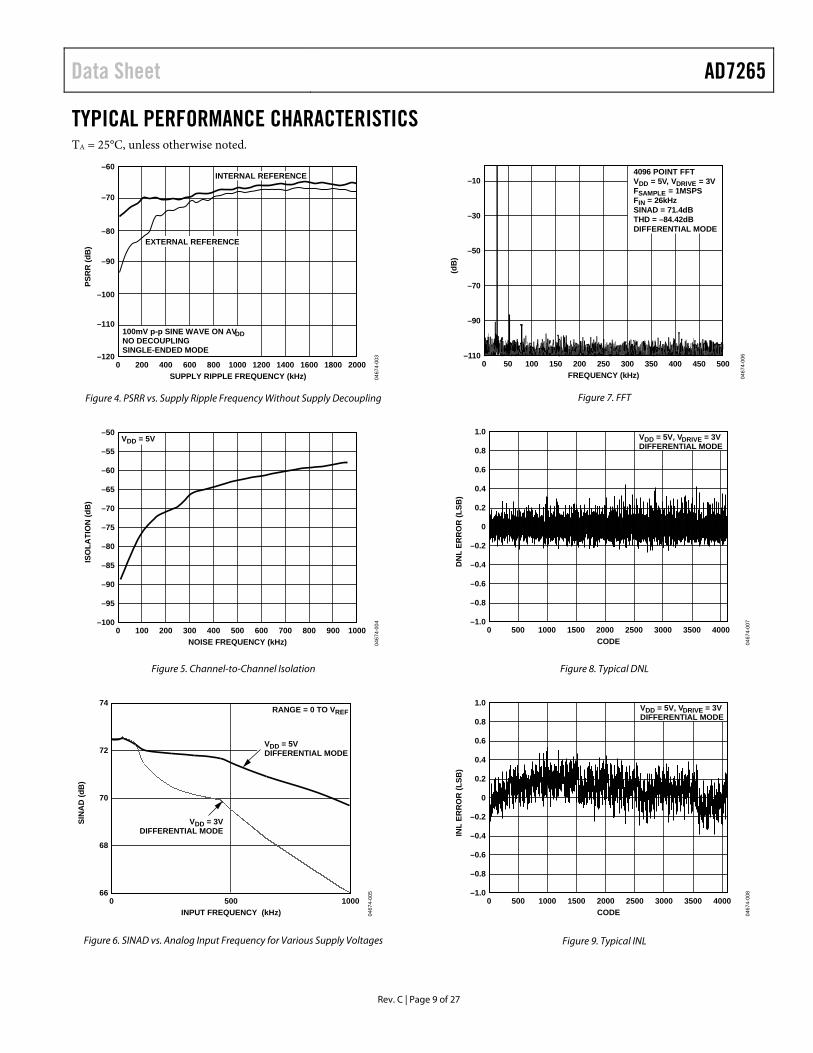
TYPICAL PERFORMANCE CHARACTERISTICS TA = 25°C, unless otherwise noted.
0467
4-00
3SUPPLY RIPPLE FREQUENCY (kHz)
20000 200 400 600 800 1000 1200 1400 1600 1800
PSR
R (d
B)
–60
–70
–80
–90
–100
–110
–120
100mV p-p SINE WAVE ON AVDDNO DECOUPLINGSINGLE-ENDED MODE
EXTERNAL REFERENCE
INTERNAL REFERENCE
Figure 4. PSRR vs. Supply Ripple Frequency Without Supply Decoupling
0467
4-00
4
NOISE FREQUENCY (kHz)10000 100 200 300 400 500 600 800700 900
ISO
LATI
ON
(dB
)
–50
–55
–60
–65
–70
–75
–90
–95
–80
–85
–100
VDD = 5V
Figure 5. Channel-to-Channel Isolation
0467
4-00
5
INPUT FREQUENCY (kHz)10000 500
SIN
AD
(dB
)
74
72
68
70
66
VDD = 5VDIFFERENTIAL MODE
VDD = 3VDIFFERENTIAL MODE
RANGE = 0 TO VREF
Figure 6. SINAD vs. Analog Input Frequency for Various Supply Voltages
0467
4-00
6
FREQUENCY (kHz)5000 50 100 150 200 250 300 350 400 450
(dB
)
–10
–30
–50
–70
–90
–110
4096 POINT FFTVDD = 5V, VDRIVE = 3VFSAMPLE = 1MSPSFIN = 26kHzSINAD = 71.4dBTHD = –84.42dBDIFFERENTIAL MODE
Figure 7. FFT
0467
4-00
7
CODE40000 1000 2000 3000 3500500 1500 2500
DN
L ER
RO
R (L
SB)
1.0
0.6
0.8
0.2
0.4
–0.2
0
–0.6
–0.8
–0.4
–1.0
VDD = 5V, VDRIVE = 3VDIFFERENTIAL MODE
Figure 8. Typical DNL
0467
4-00
8
CODE40000 500 1000 1500 2000 2500 3000 3500
INL
ERR
OR
(LSB
)
1.0
0.8
0.6
0.4
0.2
0
–0.2
–0.4
–0.6
–0.8
–1.0
VDD = 5V, VDRIVE = 3VDIFFERENTIAL MODE
Figure 9. Typical INL

AD7265 Data Sheet
Rev. C | Page 10 of 27
0467
4-00
9
VREF (V)2.50 0.5 1.0 1.5 2.0
LIN
EAR
ITY
ERR
OR
(LSB
)
1.0
0.6
0.8
0.2
0.4
–0.2
0
–0.6
–0.4
–1.0
–0.8
VDD = 3V/5VDIFFERENTIAL MODE
POSITIVE INL
POSITIVE DNL
NEGATIVE DNL
NEGATIVE INL
Figure 10. Linearity Error vs. VREF
0467
4-01
0
VREF (V)5.00 0.5 1.0 1.5 2.0 2.5 3.0 3.5 4.0 4.5
EFFE
CTI
VE N
UM
BER
OF
BIT
S
12.0
11.0
11.5
10.0
10.5
9.0
9.5
8.0
7.5
8.5
7.0
VDD = 5VDIFFERENTIAL MODE
VDD = 3VDIFFERENTIAL MODE
VDD = 3VSINGLE-ENDED MODE
VDD = 5VSINGLE-ENDED MODE
Figure 11. Effective Number of Bits vs. VREF
0467
4-01
1
CURRENT LOAD (µA)2000 20 40 60 80 100 120 140 160 180
V REF
(V)
2.5010
2.5000
2.5005
2.4995
2.4990
2.4985
2.4980
Figure 12. VREF vs. Reference Output Current Drive
0467
4-01
2
CODE2046 2047 20492048 2050
NO
. OF
OC
CU
RR
ENC
ES
10000
8000
9000
6000
7000
4000
5000
2000
1000
3000
0
10000CODES
DIFFERENTIALMODE
INTERNALREFERENCE
Figure 13. Histogram of Codes for 10k Samples in Differential Mode
0467
4-04
2
CODE2046 2047 2048 2049 2050
NO
. OF
OC
CU
RR
ENC
ES
10000
9000
8000
7000
6000
5000
4000
3000
2000
1000
0
9984CODES
SINGLE-ENDEDMODE
INTERNALREFERENCE
5 CODES 11 CODES
Figure 14. Histogram of Codes for 10k Samples in Single-Ended Mode
0467
4-04
0
RIPPLE FREQUENCY (kHz)12000 200 400 600 800 1000
CM
RR
(dB
)
–60
–65
–70
–75
–80
–85
–95
–90
–100
DIFFERENTIAL MODEVDD = 3V/5V
Figure 15. CMRR vs. Common-Mode Ripple Frequency
Data Sheet AD7265
Rev. C | Page 11 of 27
TERMINOLOGY Differential Nonlinearity (DNL) Differential nonlinearity is the difference between the measured and the ideal 1 LSB change between any two adjacent codes in the ADC.
Integral Nonlinearity (INL) Integral nonlinearity is the maximum deviation from a straight line passing through the endpoints of the ADC transfer function. The endpoints of the transfer function are zero scale with a single (1) LSB point below the first code transition, and full scale with a 1 LSB point above the last code transition.
Offset Error Offset error applies to straight binary output coding. It is the deviation of the first code transition (00 . . . 000) to (00 . . . 001) from the ideal (AGND + 1 LSB).
Offset Error Match Offset error match is the difference in offset error across all 12 channels.
Gain Error Gain error applies to straight binary output coding. It is the deviation of the last code transition (111 . . . 110) to (111 . . . 111) from the ideal (VREF − 1 LSB) after the offset error is adjusted out. Gain error does not include reference error.
Gain Error Match Gain error match is the difference in gain error across all 12 channels.
Zero Code Error Zero code error applies when using twos complement output coding with, for example, the 2 × VREF input range as −VREF to +VREF biased about the VREF point. It is the deviation of the midscale transition (all 1s to all 0s) from the ideal VIN voltage (VREF).
Zero Code Error Match Zero code error match refers to the difference in zero code error across all 12 channels.
Positive Gain Error This applies when using twos complement output coding with, for example, the 2 × VREF input range as −VREF to +VREF biased about the VREF point. It is the deviation of the last code transition (011…110) to (011…111) from the ideal (+VREF − 1 LSB) after the zero code error is adjusted out.
Track-and-Hold Acquisition Time The track-and-hold amplifier returns to track mode after the end of conversion. Track-and-hold acquisition time is the time required for the output of the track-and-hold amplifier to reach its final value, within ±1/2 LSB, after the end of conversion.
Signal-to-(Noise + Distortion) Ratio (SINAD) SINAD is the measured ratio of signal-to-(noise + distortion) at the output of the ADC. The signal is the rms amplitude of the fundamental. Noise is the sum of all non-fundamental signals up to half the sampling frequency (fS/2), excluding dc. The ratio is dependent on the number of quantization levels in the digitization process; the more levels, the smaller the quantization noise. The theoretical signal-to-(noise + distortion) ratio for an ideal N-bit converter with a sine wave input is given by
Signal-to-(Noise + Distortion) = (6.02N + 1.76) dB
Therefore, for a 12-bit converter, this is 74 dB.
Total Harmonic Distortion (THD) Total harmonic distortion is the ratio of the rms sum of harmonics to the fundamental. For the AD7265, it is defined as
1
26
25
24
23
22log20)(
VVVVVV
dBTHD++++
=
where: V1 is the rms amplitude of the fundamental. V2, V3, V4, V5, and V6 are the rms amplitudes of the second through the sixth harmonics.
Peak Harmonic or Spurious Noise Peak harmonic, or spurious noise, is defined as the ratio of the rms value of the next largest component in the ADC output spectrum (up to fS/2, excluding dc) to the rms value of the funda-mental. Normally, the value of this specification is determined by the largest harmonic in the spectrum, but for ADCs where the harmonics are buried in the noise floor, it is a noise peak.
Channel-to-Channel Isolation Channel-to-channel isolation is a measure of the level of crosstalk between channels. It is measured by applying a full-scale (2 × VREF when VDD = 5 V , and VREF when VDD = 3 V), 10 kHz sine wave signal to all unselected input channels and determining how much that signal is attenuated in the selected channel with a 50 kHz signal (0 V to VREF). The result obtained is the worst-case across all 12 channels for the AD7265.
Intermodulation Distortion With inputs consisting of sine waves at two frequencies, fa and fb, any active device with nonlinearities creates distortion products at sum, and difference frequencies of mfa ± nfb where m, n = 0, 1, 2, 3, and so on. Intermodulation distortion terms are those for which neither m nor n are equal to zero. For example, the second-order terms include (fa + fb) and (fa − fb), while the third-order terms include (2fa + fb), (2fa − fb), (fa + 2fb), and (fa − 2fb).
AD7265 Data Sheet
Rev. C | Page 12 of 27
The AD7265 is tested using the CCIF standard where two input frequencies near the top end of the input bandwidth are used. In this case, the second-order terms are usually distanced in frequency from the original sine waves, while the third-order terms are usually at a frequency close to the input frequencies. As a result, the second-order and third-order terms are specified separately. The calculation of the intermodulation distortion is as per the THD specification, where it is the ratio of the rms sum of the individual distortion products to the rms amplitude of the sum of the fundamentals expressed in dBs.
Common-Mode Rejection Ratio (CMRR) CMRR is defined as the ratio of the power in the ADC output at full-scale frequency, f, to the power of a 100 mV p-p sine wave applied to the common-mode voltage of VIN+ and VIN− of frequency fS as
CMRR (dB) = 10 log(Pf/PfS)
where: Pf is the power at frequency f in the ADC output. PfS is the power at frequency fS in the ADC output.
Power Supply Rejection Ratio (PSRR) Variations in power supply affect the full-scale transition but not the linearity of the converter. PSRR is the maximum change in the full-scale transition point due to a change in power supply voltage from the nominal value (see Figure 4).
Thermal Hysteresis Thermal hysteresis is defined as the absolute maximum change of reference output voltage after the device is cycled through temperature from either
T_HYS+ = +25°C to TMAX to +25°C
or
T_HYS− = +25°C to TMIN to +25°C
It is expressed in ppm by
610)C25(
)_()C25()( ×
°−°
=REF
REFREFHYS V
HYSTVVppmV
where: VREF (25°C) is VREF at 25°C. VREF (T_HYS) is the maximum change of VREF at T_HYS+ or T_HYS−.
Data Sheet AD7265
Rev. C | Page 13 of 27
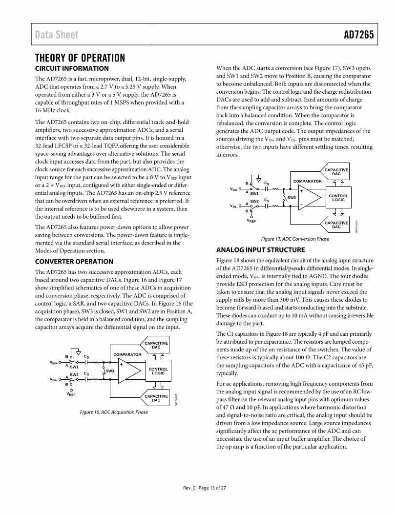
THEORY OF OPERATION CIRCUIT INFORMATION The AD7265 is a fast, micropower, dual, 12-bit, single-supply, ADC that operates from a 2.7 V to a 5.25 V supply. When operated from either a 3 V or a 5 V supply, the AD7265 is capable of throughput rates of 1 MSPS when provided with a 16 MHz clock.
The AD7265 contains two on-chip, differential track-and-hold amplifiers, two successive approximation ADCs, and a serial interface with two separate data output pins. It is housed in a 32-lead LFCSP or a 32-lead TQFP, offering the user considerable space-saving advantages over alternative solutions. The serial clock input accesses data from the part, but also provides the clock source for each successive approximation ADC. The analog input range for the part can be selected to be a 0 V to VREF input or a 2 × VREF input, configured with either single-ended or differ-ential analog inputs. The AD7265 has an on-chip 2.5 V reference that can be overdriven when an external reference is preferred. If the internal reference is to be used elsewhere in a system, then the output needs to be buffered first.
The AD7265 also features power-down options to allow power saving between conversions. The power-down feature is imple-mented via the standard serial interface, as described in the Modes of Operation section.
CONVERTER OPERATION The AD7265 has two successive approximation ADCs, each based around two capacitive DACs. Figure 16 and Figure 17 show simplified schematics of one of these ADCs in acquisition and conversion phase, respectively. The ADC is comprised of control logic, a SAR, and two capacitive DACs. In Figure 16 (the acquisition phase), SW3 is closed, SW1 and SW2 are in Position A, the comparator is held in a balanced condition, and the sampling capacitor arrays acquire the differential signal on the input.
CAPACITIVEDAC
CAPACITIVEDAC
CONTROLLOGIC
COMPARATOR
SW3SW1
A
A
B
B
SW2
CS
CS
VIN+
VIN–
VREF
0467
4-01
3
Figure 16. ADC Acquisition Phase
When the ADC starts a conversion (see Figure 17), SW3 opens and SW1 and SW2 move to Position B, causing the comparator to become unbalanced. Both inputs are disconnected when the conversion begins. The control logic and the charge redistribution DACs are used to add and subtract fixed amounts of charge from the sampling capacitor arrays to bring the comparator back into a balanced condition. When the comparator is rebalanced, the conversion is complete. The control logic generates the ADC output code. The output impedances of the sources driving the VIN+ and VIN− pins must be matched; otherwise, the two inputs have different settling times, resulting in errors.
CAPACITIVEDAC
CAPACITIVEDAC
CONTROLLOGIC
COMPARATOR
SW3SW1
A
A
B
B
SW2
CS
CS
VIN+
VIN–
VREF
0467
4-01
4
Figure 17. ADC Conversion Phase
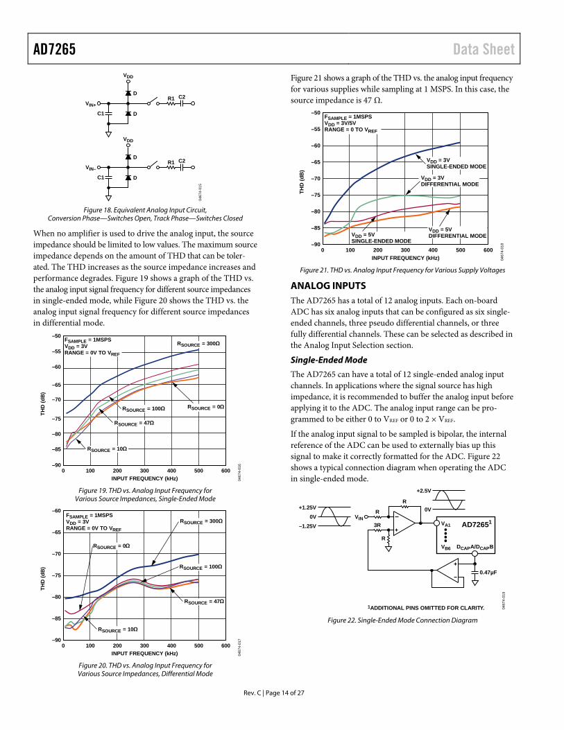
ANALOG INPUT STRUCTURE Figure 18 shows the equivalent circuit of the analog input structure of the AD7265 in differential/pseudo differential modes. In single-ended mode, VIN− is internally tied to AGND. The four diodes provide ESD protection for the analog inputs. Care must be taken to ensure that the analog input signals never exceed the supply rails by more than 300 mV. This causes these diodes to become forward-biased and starts conducting into the substrate. These diodes can conduct up to 10 mA without causing irreversible damage to the part.
The C1 capacitors in Figure 18 are typically 4 pF and can primarily be attributed to pin capacitance. The resistors are lumped compo-nents made up of the on resistance of the switches. The value of these resistors is typically about 100 Ω. The C2 capacitors are the sampling capacitors of the ADC with a capacitance of 45 pF, typically.
For ac applications, removing high frequency components from the analog input signal is recommended by the use of an RC low-pass filter on the relevant analog input pins with optimum values of 47 Ω and 10 pF. In applications where harmonic distortion and signal-to-noise ratio are critical, the analog input should be driven from a low impedance source. Large source impedances significantly affect the ac performance of the ADC and can necessitate the use of an input buffer amplifier. The choice of the op amp is a function of the particular application.
AD7265 Data Sheet
Rev. C | Page 14 of 27
VDD
C1
D
D
VIN+R1 C2
VDD
C1
D
D
VIN–R1 C2
0467
4-01
5
Figure 18. Equivalent Analog Input Circuit, Conversion Phase—Switches Open, Track Phase—Switches Closed
When no amplifier is used to drive the analog input, the source impedance should be limited to low values. The maximum source impedance depends on the amount of THD that can be toler-ated. The THD increases as the source impedance increases and performance degrades. Figure 19 shows a graph of the THD vs. the analog input signal frequency for different source impedances in single-ended mode, while Figure 20 shows the THD vs. the analog input signal frequency for different source impedances in differential mode.
0467
4-01
6
INPUT FREQUENCY (kHz)6000 200100 400300 500
THD
(dB
)
–50
–60
–55
–65
–70
–75
–80
–85
–90
FSAMPLE = 1MSPSVDD = 3VRANGE = 0V TO VREF
RSOURCE = 0Ω
RSOURCE = 10Ω
RSOURCE = 47Ω
RSOURCE = 100Ω
RSOURCE = 300Ω
Figure 19. THD vs. Analog Input Frequency for
Various Source Impedances, Single-Ended Mode
0467
4-01
7
INPUT FREQUENCY (kHz)6000 200100 400300 500
THD
(dB
)
–60
–65
–70
–75
–80
–85
–90
FSAMPLE = 1MSPSVDD = 3VRANGE = 0V TO VREF
RSOURCE = 300Ω
RSOURCE = 0Ω
RSOURCE = 10Ω
RSOURCE = 47Ω
RSOURCE = 100Ω
Figure 20. THD vs. Analog Input Frequency for Various Source Impedances, Differential Mode
Figure 21 shows a graph of the THD vs. the analog input frequency for various supplies while sampling at 1 MSPS. In this case, the source impedance is 47 Ω.
0467
4-01
8
INPUT FREQUENCY (kHz)6000 200100 400300 500
THD
(dB
)
–50
–60
–55
–65
–70
–75
–80
–85
–90
VDD = 3VSINGLE-ENDED MODE
VDD = 5VSINGLE-ENDED MODE
VDD = 3VDIFFERENTIAL MODE
VDD = 5VDIFFERENTIAL MODE
FSAMPLE = 1MSPSVDD = 3V/5VRANGE = 0 TO VREF
Figure 21. THD vs. Analog Input Frequency for Various Supply Voltages
ANALOG INPUTS The AD7265 has a total of 12 analog inputs. Each on-board ADC has six analog inputs that can be configured as six single-ended channels, three pseudo differential channels, or three fully differential channels. These can be selected as described in the Analog Input Selection section.
Single-Ended Mode
The AD7265 can have a total of 12 single-ended analog input channels. In applications where the signal source has high impedance, it is recommended to buffer the analog input before applying it to the ADC. The analog input range can be pro-grammed to be either 0 to VREF or 0 to 2 × VREF.
If the analog input signal to be sampled is bipolar, the internal reference of the ADC can be used to externally bias up this signal to make it correctly formatted for the ADC. Figure 22 shows a typical connection diagram when operating the ADC in single-ended mode.
VIN0V+1.25V
–1.25V
DCAPA/DCAPB
VA1
VB6
R
R
3R
R
0V
+2.5V
0.47µF
1ADDITIONAL PINS OMITTED FOR CLARITY. 0467
4-01
9
AD72651
Figure 22. Single-Ended Mode Connection Diagram
Data Sheet AD7265
Rev. C | Page 15 of 27
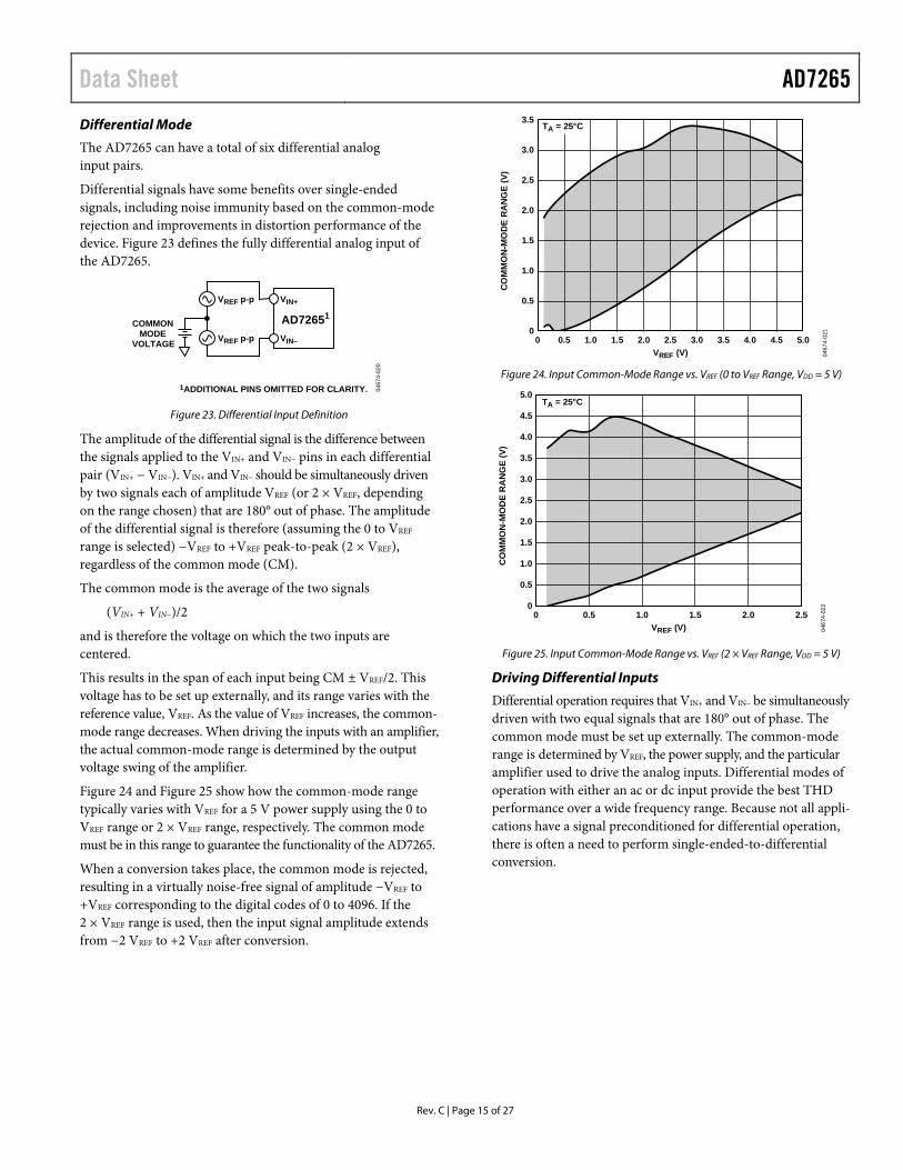
Differential Mode
The AD7265 can have a total of six differential analog input pairs.
Differential signals have some benefits over single-ended signals, including noise immunity based on the common-mode rejection and improvements in distortion performance of the device. Figure 23 defines the fully differential analog input of the AD7265.
VIN+
VIN–
VREF p-p
VREF p-pCOMMON
MODEVOLTAGE
1ADDITIONAL PINS OMITTED FOR CLARITY. 0467
4-02
0
AD72651
Figure 23. Differential Input Definition
The amplitude of the differential signal is the difference between the signals applied to the VIN+ and VIN− pins in each differential pair (VIN+ − VIN−). VIN+ and VIN− should be simultaneously driven by two signals each of amplitude VREF (or 2 × VREF, depending on the range chosen) that are 180° out of phase. The amplitude of the differential signal is therefore (assuming the 0 to VREF range is selected) −VREF to +VREF peak-to-peak (2 × VREF), regardless of the common mode (CM).
The common mode is the average of the two signals
(VIN+ + VIN−)/2
and is therefore the voltage on which the two inputs are centered.
This results in the span of each input being CM ± VREF/2. This voltage has to be set up externally, and its range varies with the reference value, VREF. As the value of VREF increases, the common-mode range decreases. When driving the inputs with an amplifier, the actual common-mode range is determined by the output voltage swing of the amplifier.
Figure 24 and Figure 25 show how the common-mode range typically varies with VREF for a 5 V power supply using the 0 to VREF range or 2 × VREF range, respectively. The common mode must be in this range to guarantee the functionality of the AD7265.
When a conversion takes place, the common mode is rejected, resulting in a virtually noise-free signal of amplitude −VREF to +VREF corresponding to the digital codes of 0 to 4096. If the 2 × VREF range is used, then the input signal amplitude extends from −2 VREF to +2 VREF after conversion.
0467
4-02
1
VREF (V)5.00 0.5 1.0 1.5 2.0 2.5 3.0 3.5 4.0 4.5
CO
MM
ON
-MO
DE
RA
NG
E (V
)
3.5
3.0
2.5
2.0
1.5
1.0
0.5
0
TA = 25°C
Figure 24. Input Common-Mode Range vs. VREF (0 to VREF Range, VDD = 5 V)
0467
4-02
2
VREF (V)2.50 0.5 1.0 1.5 2.0
CO
MM
ON
-MO
DE
RA
NG
E (V
)
5.0
4.0
4.5
3.0
3.5
2.0
2.5
0.5
1.0
1.5
0
TA = 25°C
Figure 25. Input Common-Mode Range vs. VREF (2 × VREF Range, VDD = 5 V)
Driving Differential Inputs
Differential operation requires that VIN+ and VIN− be simultaneously driven with two equal signals that are 180° out of phase. The common mode must be set up externally. The common-mode range is determined by VREF, the power supply, and the particular amplifier used to drive the analog inputs. Differential modes of operation with either an ac or dc input provide the best THD performance over a wide frequency range. Because not all appli-cations have a signal preconditioned for differential operation, there is often a need to perform single-ended-to-differential conversion.
AD7265 Data Sheet
Rev. C | Page 16 of 27
Using an Op Amp Pair
An op amp pair can be used to directly couple a differential signal to one of the analog input pairs of the AD7265. The circuit configurations illustrated in Figure 26 and Figure 27 show how a dual op amp can be used to convert a single-ended signal into a differential signal for both a bipolar and unipolar input signal, respectively.
The voltage applied to Point A sets up the common-mode voltage. In both diagrams, it is connected in some way to the reference, but any value in the common-mode range can be input here to set up the common mode. The AD8022 is a suitable dual op amp that can be used in this configuration to provide differential drive to the AD7265.
Take care when choosing the op amp; the selection depends on the required power supply and system performance objectives. The driver circuits in Figure 26 and Figure 27 are optimized for dc coupling applications requiring best distortion performance.
The circuit configuration shown in Figure 26 converts a unipolar, single-ended signal into a differential signal.
The differential op amp driver circuit shown in Figure 27 is configured to convert and level shift a single-ended, ground-referenced (bipolar) signal to a differential signal centered at the VREF level of the ADC.
GND
2 × VREF p-p
27Ω
27ΩV+
V–
V+
V–
VREF
2.5V
3.75V
1.25V
2.5V
3.75V
1.25V
DCAPA/DCAPB
VIN+
VIN–
440Ω
220Ω
0.47µF
1ADDITIONAL PINS OMITTED FOR CLARITY.
220Ω220Ω
10kΩ
A
0467
4-02
3
AD72651
Figure 26. Dual Op Amp Circuit to Convert a Single-Ended Unipolar Signal
into a Differential Signal
20kΩ
220kΩ
2 × VREF p-p
27Ω
27ΩV+
V–
V+
V–
GND
2.5V
3.75V
1.25V
2.5V
3.75V
1.25V
DCAPA/DCAPB
VIN+
VIN–
440Ω
220Ω
0.47µF
1ADDITIONAL PINS OMITTED FOR CLARITY.
220Ω220Ω
10kΩ
A
0467
4-02
4
AD72651
Figure 27. Dual Op Amp Circuit to Convert a Single-Ended Bipolar Signal
into a Differential Unipolar Signal
Pseudo Differential Mode
The AD7265 can have a total of six pseudo differential pairs. In this mode, VIN+ is connected to the signal source that must have an amplitude of VREF (or 2 × VREF, depending on the range chosen) to make use of the full dynamic range of the part. A dc input is applied to the VIN− pin. The voltage applied to this input provides an offset from ground or a pseudo ground for the VIN+ input. The benefit of pseudo differential inputs is that they separate the analog input signal ground from the ADC’s ground allowing dc common-mode voltages to be cancelled. The typical voltage range for the VIN− pin, while in pseudo differential mode, is shown in Figure 28 and Figure 29. Figure 30 shows a connection diagram for pseudo differential mode.
0467
4-04
3
VREF (V)
3.00 0.5 1.0 1.5 2.0 2.5
VIN
– (V
)
1.0
0.8
0.4
0.6
0.2
–0.2
0
–0.4
TA = 25°C
Figure 28. VIN− Input Voltage Range vs. VREF in
Pseudo Differential Mode with VDD = 3 V
0467
4-04
4
VREF (V)
5.00 0.5 1.0 1.5 2.0 2.5 3.0 3.5 4.0 4.5
VIN
– (V
)
2.5
2.0
1.5
1.0
0.5
0
–0.5
TA = 25°C
Figure 29. VIN− Input Voltage Range vs. VREF in
Pseudo Differential Mode with VDD = 5 V
DC INPUTVOLTAGE
VREFp–p
VREF
VIN+
VIN–
0.47µF
1ADDITIONAL PINS OMITTED FOR CLARITY. 0467
4-02
5
AD72651
Figure 30. Pseudo Differential Mode Connection Diagram
Data Sheet AD7265
Rev. C | Page 17 of 27
ANALOG INPUT SELECTION The analog inputs of the AD7265 can be configured as single-ended or true differential via the SGL/DIFF logic pin, as shown in Figure 31. If this pin is tied to a logic low, the analog input channels to each on-chip ADC are set up as three true differen-tial pairs. If this pin is at logic high, the analog input channels to each on-chip ADC are set up as six single-ended analog inputs. The required logic level on this pin needs to be established prior to the acquisition time and remain unchanged during the con-version time until the track-and-hold has returned to track. The track-and-hold returns to track on the 13th rising edge of SCLK after the CS falling edge (see Figure 41). If the level on this pin is changed, it is recognized by the AD7265; therefore, it is necessary to keep the same logic level during acquisition and conversion to avoid corrupting the conversion in progress.
For example, in Figure 31, the SGL/DIFF pin is set at logic high for the duration of both the acquisition and conversion times so the analog inputs are configured as single ended for that conversion (Sampling Point A). The logic level of the SGL/DIFF changed to low after the track-and-hold returned to track and prior to the required acquisition time for the next sampling instant at Point B; therefore, the analog inputs are configured as differential for that conversion.
SCLK
CS
1 14 141
A
SGL/DIFF
B
tACQ
0467
4-02
6
Figure 31. Selecting Differential or Single-Ended Configuration
The channels used for simultaneous conversions are selected via the multiplexer address input pins, A0 to A2. The logic states of these pins also need to be established prior to the acquisition time; however, they can change during the conversion time, provided that the mode is not changed. If the mode is changed from fully differential to pseudo-differential, for example, then the acquisition time starts again from this point. The selected input channels are decoded as shown in Table 6.
The analog input range of the AD7265 can be selected as 0 V to VREF or 0 V to 2 × VREF via the RANGE pin. This selection is made in a similar fashion to that of the SGL/DIFF pin by setting the logic state of the RANGE pin a time tacq prior to the falling edge of CS. Subsequent to this, the logic level on this pin can be altered after the third falling edge of SCLK. If this pin is tied to a logic low, the analog input range selected is 0 V to VREF. If this pin is tied to a logic high, the analog input range selected is 0 V to 2 × VREF.
OUTPUT CODING The AD7265 output coding is set to either twos complement or straight binary, depending on which analog input configuration is selected for a conversion. Table 5 shows which output coding scheme is used for each possible analog input configuration.
Table 5. AD7265 Output Coding SGL/DIFF Range Output Coding
DIFF 0 V to VREF Twos complement DIFF 0 V to 2 × VREF Twos complement SGL 0 V to VREF Straight binary SGL 0 V to 2 × VREF Twos complement PSEUDO DIFF 0 V to VREF Straight binary PSEUDO DIFF 0 V to 2 × VREF Twos complement
Table 6. Analog Input Type and Channel Selection ADC A ADC B
SGL/DIFF A2 A1 A0 VIN+ VIN− VIN+ VIN− Comment
1 0 0 0 VA1 AGND VB1 AGND Single ended 1 0 0 1 VA2 AGND VB2 AGND Single ended 1 0 1 0 VA3 AGND VB3 AGND Single ended 1 0 1 1 VA4 AGND VB4 AGND Single ended 1 1 0 0 VA5 AGND VB5 AGND Single ended 1 1 0 1 VA6 AGND VB6 AGND Single ended 0 0 0 0 VA1 VA2 VB1 VB2 Fully differential 0 0 0 1 VA1 VA2 VB1 VB2 Pseudo differential 0 0 1 0 VA3 VA4 VB3 VB4 Fully differential 0 0 1 1 VA3 VA4 VB3 VB4 Pseudo differential 0 1 0 0 VA5 VA6 VB5 VB6 Fully differential 0 1 0 1 VA5 VA6 VB5 VB6 Pseudo differential
AD7265 Data Sheet
Rev. C | Page 18 of 27
TRANSFER FUNCTIONS The designed code transitions occur at successive integer LSB values (1 LSB, 2 LSB, and so on). In single-ended mode, the LSB size is VREF/4096 when the 0 V to VREF range is used, and the LSB size is 2 × VREF/4096 when the 0 V to 2 × VREF range is used. In differential mode, the LSB size is 2 × VREF/4096 when the 0 V to VREF range is used, and the LSB size is 4 × VREF/4096 when the 0 V to 2 × VREF range is used. The ideal transfer characteristic for the AD7265 when straight binary coding is output is shown in Figure 32, and the ideal transfer characteristic for the AD7265 when twos complement coding is output is shown (with the 2 × VREF range) in Figure 33.
0467
4-02
7
000...000
111...111
1LSB = VREF/4096
1LSB VREF – 1LSB
ANALOG INPUT
AD
C C
OD
E
0V
000...001
000...010
111...110
111...000
011...111
NOTE1. VREF IS EITHER VREF OR 2 × VREF.
Figure 32. Straight Binary Transfer Characteristic
0467
4-02
8100...000
011...111
1LSB = 2 VREF/4096
+VREF – 1 LSB–VREF + 1LSB VREF – 1LSB
ANALOG INPUT
AD
C C
OD
E
100...001
100...010
011...110
000...001
000...000
111...111
Figure 33. Twos Complement Transfer Characteristic with
VREF ± VREF Input Range
DIGITAL INPUTS The digital inputs applied to the AD7265 are not limited by the maximum ratings that limit the analog inputs. Instead, the digital inputs can be applied up to 7 V and are not restricted by the VDD + 0.3 V limit, as are the analog inputs. See the Absolute Maximum Ratings section for more information. Another advantage of the SCLK, RANGE, A0 to A2, and CS pins not being restricted by the VDD + 0.3 V limit is that power supply sequencing issues are avoided. If one of these digital inputs is applied before VDD, there is no risk of latch-up, as there would be on the analog inputs if a signal greater than 0.3 V were applied prior to VDD.
VDRIVE The AD7265 also has a VDRIVE feature to control the voltage at which the serial interface operates. VDRIVE allows the ADC to easily interface to both 3 V and 5 V processors. For example, if the AD7265 was operated with a VDD of 5 V, the VDRIVE pin can be powered from a 3 V supply, allowing a large dynamic range with low voltage digital processors. Therefore, the AD7265 can be used with the 2 × VREF input range, with a VDD of 5 V while still being able to interface to 3 V digital parts.

Data Sheet AD7265
Rev. C | Page 19 of 27
MODES OF OPERATION The mode of operation of the AD7265 is selected by controlling the (logic) state of the CS signal during a conversion. There are three possible modes of operation: normal mode, partial power-down mode, and full power-down mode. After a conversion is initiated, the point at which CS is pulled high determines which power-down mode, if any, the device enters. Similarly, if already in a power-down mode, CS can control whether the device returns to normal operation or remains in power-down. These modes of operation are designed to provide flexible power management options. These options can be chosen to optimize the power dissipation/throughput rate ratio for differing application requirements.
NORMAL MODE This mode is intended for applications that need the fastest throughput rates because the user does not have to worry about any power-up times with the AD7265 remaining fully powered at all times. Figure 34 shows the general diagram of the operation of the AD7265 in this mode.
SCLK
LEADING ZEROS + CONVERSION RESULT
CS
DOUTADOUTB
1 1410
0467
4-02
9
Figure 34. Normal Mode Operation
The conversion is initiated on the falling edge of CS, as described in the Serial Interface section. To ensure that the part remains fully powered up at all times, CS must remain low until at least 10 SCLK falling edges have elapsed after the falling edge of CS. If CS is brought high any time after the 10th SCLK falling edge but before the 14th SCLK falling edge, the part remains powered up, but the conversion is terminated and DOUTA and DOUTB go back into three-state. Fourteen serial clock cycles are required to complete the conversion and access the conversion result. The DOUT line does not return to three-state after 14 SCLK cycles have elapsed, but instead does so when CS is brought high again. If CS is left low for another 2 SCLK cycles (for example, if only a 16 SCLK burst is available), two trailing zeros are clocked out after the data. If CS is left low for a further 14 (or 16) SCLK cycles, the result from the other ADC on board is also accessed on the same DOUT line, as shown in Figure 42 (see the Serial Interface section).
When 32 SCLK cycles have elapsed, the DOUT line returns to three-state on the 32nd SCLK falling edge. If CS is brought high prior to this, the DOUT line returns to three-state at that point. There-fore, CS can idle low after 32 SCLK cycles until it is brought high again sometime prior to the next conversion (effectively idling CS low), if so desired, because the bus still returns to three-state upon completion of the dual result read.
When a data transfer is complete and DOUTA and DOUTB have returned to three-state, another conversion can be initiated after the quiet time, tQUIET, has elapsed by bringing CS low again (assuming the required acquisition time is allowed).
PARTIAL POWER-DOWN MODE This mode is intended for use in applications where slower throughput rates are required. Either the ADC is powered down between each conversion, or a series of conversions can be performed at a high throughput rate, and the ADC is then powered down for a relatively long duration between these bursts of several conversions. When the AD7265 is in partial power-down, all analog circuitry is powered down except for the on-chip reference and reference buffer.
To enter partial power-down mode, the conversion process must be interrupted by bringing CS high anywhere after the second falling edge of SCLK and before the 10th falling edge of SCLK, as shown in Figure 35. When CS is brought high in this window of SCLKs, the part enters partial power-down, the conversion that was initiated by the falling edge of CS is terminated, and DOUTA and DOUTB go back into three-state. If CS is brought high before the second SCLK falling edge, the part remains in normal mode and does not power down. This avoids accidental power-down due to glitches on the CS line.
SCLK
THREE-STATE
CS
DOUTADOUTB
1 14102
0467
4-03
0
Figure 35. Entering Partial Power-Down Mode
AD7265 Data Sheet
Rev. C | Page 20 of 27
To exit this mode of operation and power up the AD7265 again, a dummy conversion is performed. On the falling edge of CS, the device begins to power up and continues to power up as long as CS is held low until after the falling edge of the 10th SCLK. The device is fully powered up after approximately 1 μs has elapsed, and valid data results from the next conversion, as shown in Figure 36. If CS is brought high before the second falling edge of SCLK, the AD7265 again goes into partial power-down. This avoids accidental power-up due to glitches on the CS line. Although the device can begin to power up on the falling edge of CS, it powers down again on the rising edge of CS. If the AD7265 is already in partial power-down mode and CS is brought high between the second and 10th falling edges of SCLK, the device enters full power-down mode.
FULL POWER-DOWN MODE This mode is intended for use in applications where throughput rates slower than those in the partial power-down mode are required, as power-up from a full power-down takes substantially longer than that from partial power-down. This mode is more suited to applications where a series of conversions performed at a relatively high throughput rate are followed by a long period of inactivity and thus power-down.
When the AD7265 is in full power-down, all analog circuitry is powered down. Full power-down is entered in a similar way as partial power-down, except the timing sequence shown in Figure 35 must be executed twice. The conversion process must be interrupted in a similar fashion by bringing CS high anywhere after the second falling edge of SCLK and before the 10th falling edge of SCLK. The device enters partial power-down at this point. To reach full power-down, the next conversion cycle must be interrupted in the same way, as shown in Figure 37. When CS is brought high in this window of SCLKs, the part completely powers down.
Note that it is not necessary to complete the 14 SCLKs when CS is brought high to enter a power-down mode.
To exit full power-down and power up the AD7265, a dummy conversion is performed, as when powering up from partial power-down. On the falling edge of CS, the device begins to power up and continues to power up, as long as CS is held low until after the falling edge of the 10th SCLK. The required power-up time must elapse before a conversion can be initiated, as shown in Figure 38. See the Power-Up Times section for the power-up times associated with the AD7265.
SCLK
CS
DOUTA
DOUTBINVALID DATA VALID DATA
1 10 14 141
THE PART BEGINSTO POWER UP.
THE PART IS FULLYPOWERED UP; SEEPOWER-UP TIMESSECTION.tPOWER-UP1
0467
4-03
1
Figure 36. Exiting Partial Power-Down Mode
THREE-STATE
1 10 142SCLK
CS
DOUTA
DOUTB
THREE-STATE
1 10 142
INVALID DATAINVALID DATA
THE PART BEGINS TO POWER UP.
THE PART ENTERS PARTIAL POWER DOWN.
THE PART ENTERS FULL POWER DOWN.
0467
4-03
2
Figure 37. Entering Full Power-Down Mode
Data Sheet AD7265
Rev. C | Page 21 of 27
SCLK
DOUTA
DOUTBINVALID DATA VALID DATA
1 10 14 141
THE PART BEGINSTO POWER UP.
THE PART IS FULLY POWERED UP,SEE POWER-UP TIMES SECTION.
tPOWER-UP2
CS
0467
4-03
3
Figure 38. Exiting Full Power-Down Mode
POWER-UP TIMES As described in detail, the AD7265 has two power-down modes, partial power-down and full power-down. This section explains the power-up time required when coming out of either of these modes. Note that the power-up times, as explained in this section, apply with the recommended capacitors in place on the DCAPA and DCAPB pins.
To power up from full power-down (whether using an internal or external reference), approximately 1.5 ms should be allowed from the falling edge of CS, shown as tPOWER-UP2 in Figure 38. Powering up from partial power-down requires much less time. The power-up time from partial power-down is typically 1 μs; however, if using the internal reference, then the AD7265 must be in partial power-down for at least 67 μs in order for this power-up time to apply.
When power supplies are first applied to the AD7265, the ADC can power up in either of the power-down modes or normal mode. Because of this, it is best to allow a dummy cycle to elapse to ensure that the part is fully powered up before attempting a valid conversion. Likewise, if it is intended to keep the part in the partial power-down mode immediately after the supplies are applied, then two dummy cycles must be initiated. The first dummy cycle must hold CS low until after the 10th SCLK falling edge (see Figure 34); in the second cycle, CS must be brought high before the 10th SCLK edge but after the second SCLK falling edge (see Figure 35). Alternatively, if it is intended to place the part in full power-down mode when the supplies are applied, then three dummy cycles must be initiated. The first dummy cycle must hold CS low until after the 10th SCLK falling edge (see Figure 34); the second and third dummy cycles place the part in full power-down (see Figure 37).
When supplies are applied to the AD7265, enough time must be allowed for any external reference to power up and charge the various reference buffer decoupling capacitors to their final values.
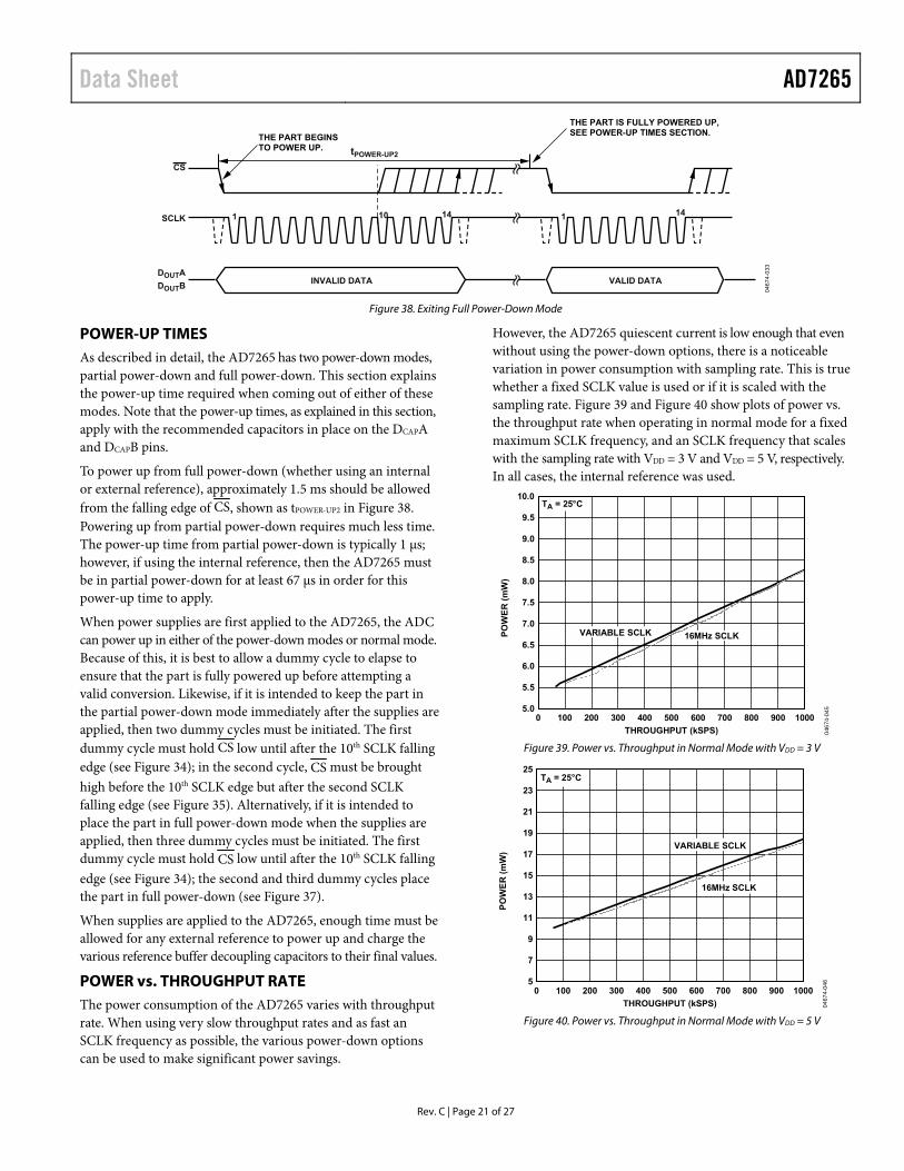
POWER vs. THROUGHPUT RATE The power consumption of the AD7265 varies with throughput rate. When using very slow throughput rates and as fast an SCLK frequency as possible, the various power-down options can be used to make significant power savings.
However, the AD7265 quiescent current is low enough that even without using the power-down options, there is a noticeable variation in power consumption with sampling rate. This is true whether a fixed SCLK value is used or if it is scaled with the sampling rate. Figure 39 and Figure 40 show plots of power vs. the throughput rate when operating in normal mode for a fixed maximum SCLK frequency, and an SCLK frequency that scales with the sampling rate with VDD = 3 V and VDD = 5 V, respectively. In all cases, the internal reference was used.
0467
4-04
5
THROUGHPUT (kSPS)
10000 100 200 300 500400 700 800 900600
PO
WE
R (
mW
)10.0
9.0
8.5
9.5
8.0
7.0
6.5
7.5
6.0
5.5
5.0
16MHz SCLKVARIABLE SCLK
TA = 25°C
Figure 39. Power vs. Throughput in Normal Mode with VDD = 3 V
0467
4-04
6
THROUGHPUT (kSPS)
10000 200 300 400100 500 600 700 800 900
PO
WE
R (
mW
)
25
21
19
23
17
13
15
9
7
11
5
VARIABLE SCLK
TA = 25°C
16MHz SCLK
Figure 40. Power vs. Throughput in Normal Mode with VDD = 5 V
AD7265 Data Sheet
Rev. C | Page 22 of 27
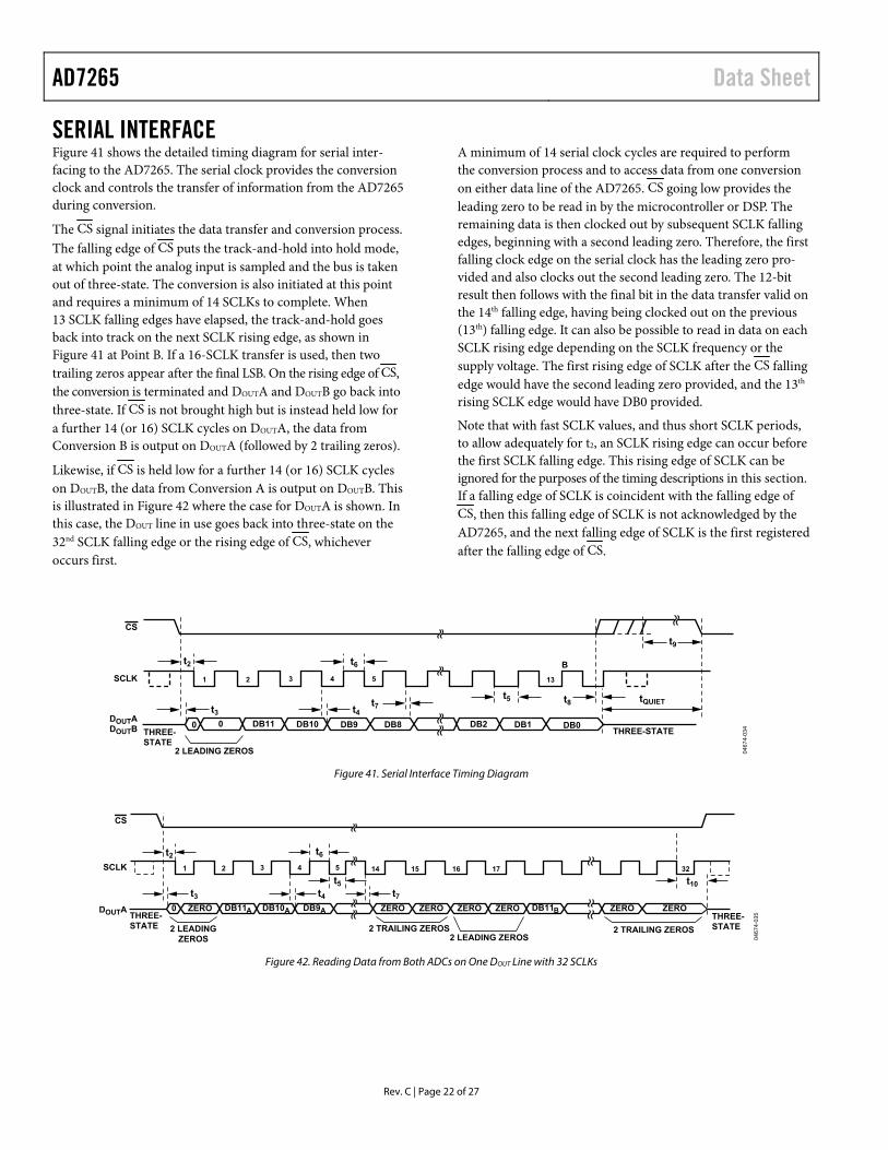
SERIAL INTERFACE Figure 41 shows the detailed timing diagram for serial inter-facing to the AD7265. The serial clock provides the conversion clock and controls the transfer of information from the AD7265 during conversion.
The CS signal initiates the data transfer and conversion process. The falling edge of CS puts the track-and-hold into hold mode, at which point the analog input is sampled and the bus is taken out of three-state. The conversion is also initiated at this point and requires a minimum of 14 SCLKs to complete. When 13 SCLK falling edges have elapsed, the track-and-hold goes back into track on the next SCLK rising edge, as shown in Figure 41 at Point B. If a 16-SCLK transfer is used, then two trailing zeros appear after the final LSB. On the rising edge of CS, the conversion is terminated and DOUTA and DOUTB go back into three-state. If CS is not brought high but is instead held low for a further 14 (or 16) SCLK cycles on DOUTA, the data from Conversion B is output on DOUTA (followed by 2 trailing zeros).
Likewise, if CS is held low for a further 14 (or 16) SCLK cycles on DOUTB, the data from Conversion A is output on DOUTB. This is illustrated in Figure 42 where the case for DOUTA is shown. In this case, the DOUT line in use goes back into three-state on the 32nd SCLK falling edge or the rising edge of CS, whichever occurs first.
A minimum of 14 serial clock cycles are required to perform the conversion process and to access data from one conversion on either data line of the AD7265. CS going low provides the leading zero to be read in by the microcontroller or DSP. The remaining data is then clocked out by subsequent SCLK falling edges, beginning with a second leading zero. Therefore, the first falling clock edge on the serial clock has the leading zero pro-vided and also clocks out the second leading zero. The 12-bit result then follows with the final bit in the data transfer valid on the 14th falling edge, having being clocked out on the previous (13th) falling edge. It can also be possible to read in data on each SCLK rising edge depending on the SCLK frequency or the supply voltage. The first rising edge of SCLK after the CS falling edge would have the second leading zero provided, and the 13th rising SCLK edge would have DB0 provided.
Note that with fast SCLK values, and thus short SCLK periods, to allow adequately for t2, an SCLK rising edge can occur before the first SCLK falling edge. This rising edge of SCLK can be ignored for the purposes of the timing descriptions in this section. If a falling edge of SCLK is coincident with the falling edge of CS, then this falling edge of SCLK is not acknowledged by the AD7265, and the next falling edge of SCLK is the first registered after the falling edge of CS.
CS
SCLK 1 5 13
DOUTADOUTB
2 LEADING ZEROS
THREE-STATE
t4
2 3 4
t5
t3
tQUIET
t2
THREE-STATEDB11 DB10 DB2 DB0
t6
t7t8
00 DB1
B
DB9 DB8
t9
0467
4-03
4
Figure 41. Serial Interface Timing Diagram
CS
SCLK 1 5 15
DOUTATHREE-STATE
t4
2 3 4 16
t5
t3
t2
THREE-STATE
t6
t7
14
ZERO0 ZERO DB11B
17
2 LEADING ZEROS
t10
32
DB11A
2 LEADINGZEROS
DB10A DB9A ZEROZERO ZERO
2 TRAILING ZEROS
ZERO ZERO
2 TRAILING ZEROS
0467
4-03
5
Figure 42. Reading Data from Both ADCs on One DOUT Line with 32 SCLKs
Data Sheet AD7265
Rev. C | Page 23 of 27
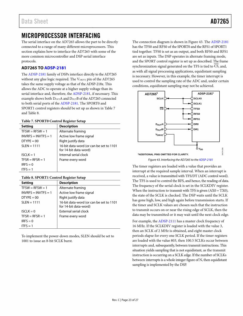
MICROPROCESSOR INTERFACING The serial interface on the AD7265 allows the part to be directly connected to a range of many different microprocessors. This section explains how to interface the AD7265 with some of the more common microcontroller and DSP serial interface protocols.
AD7265 TO ADSP-2181 The ADSP-2181 family of DSPs interface directly to the AD7265 without any glue logic required. The VDRIVE pin of the AD7265 takes the same supply voltage as that of the ADSP-218x. This allows the ADC to operate at a higher supply voltage than its serial interface and, therefore, the ADSP-2181, if necessary. This example shows both DOUTA and DOUTB of the AD7265 connected to both serial ports of the ADSP-2181. The SPORT0 and SPORT1 control registers should be set up as shown in Table 7 and Table 8.
Table 7. SPORT0 Control Register Setup Setting Description TFSW = RFSW = 1 Alternate framing INVRFS = INVTFS = 1 Active low frame signal DTYPE = 00 Right justify data SLEN = 1111 16-bit data-word (or can be set to 1101
for 14-bit data-word) ISCLK = 1 Internal serial clock TFSR = RFSR = 1 Frame every word IRFS = 0 ITFS = 1
Table 8. SPORT1 Control Register Setup Setting Description TFSW = RFSW = 1 Alternate framing INVRFS = INVTFS = 1 Active low frame signal DTYPE = 00 Right justify data SLEN = 1111 16-bit data-word (or can be set to 1101
for 14-bit data-word) ISCLK = 0 External serial clock TFSR = RFSR = 1 Frame every word IRFS = 0 ITFS = 1
To implement the power-down modes, SLEN should be set to 1001 to issue an 8-bit SCLK burst.
The connection diagram is shown in Figure 43. The ADSP-2181 has the TFS0 and RFS0 of the SPORT0 and the RFS1 of SPORT1 tied together. TFS0 is set as an output, and both RFS0 and RFS1 are set as inputs. The DSP operates in alternate framing mode, and the SPORT control register is set up as described. The frame synchronization signal generated on the TFS is tied to CS, and, as with all signal processing applications, equidistant sampling is necessary. However, in this example, the timer interrupt is used to control the sampling rate of the ADC and, under certain conditions, equidistant sampling may not be achieved.
AD72651
SCLK
CS
ADSP-21811
1ADDITIONAL PINS OMITTED FOR CLARITY.
SCLK0
DR0
RFS0
TFS0
DOUTA
VDRIVE
VDD
DOUTB DR1
RFS1
SCLK1
0467
4-03
6
Figure 43. Interfacing the AD7265 to the ADSP-2181
The timer registers are loaded with a value that provides an interrupt at the required sample interval. When an interrupt is received, a value is transmitted with TFS/DT (ADC control word). The TFS is used to control the RFS, and hence, the reading of data. The frequency of the serial clock is set in the SCLKDIV register. When the instruction to transmit with TFS is given (AX0 = TX0), the state of the SCLK is checked. The DSP waits until the SCLK has gone high, low, and high again before transmission starts. If the timer and SCLK values are chosen such that the instruction to transmit occurs on or near the rising edge of SCLK, then the data may be transmitted or it may wait until the next clock edge.
For example, the ADSP-2111 has a master clock frequency of 16 MHz. If the SCLKDIV register is loaded with the value 3, then an SCLK of 2 MHz is obtained, and eight master clock periods elapse for every one SCLK period. If the timer registers are loaded with the value 803, then 100.5 SCLKs occur between interrupts and, subsequently, between transmit instructions. This situation yields sampling that is not equidistant, as the transmit instruction is occurring on a SCLK edge. If the number of SCLKs between interrupts is a whole integer figure of N, then equidistant sampling is implemented by the DSP.

AD7265 Data Sheet
Rev. C | Page 24 of 27
AD7265 to ADSP-BF531 The ADSP-BF531 interfaces directly to the AD7265 without any glue logic required. The availability of secondary receive registers on the serial ports of the Blackfin® DSPs means only one serial port is necessary to read from both DOUT pins simultaneously. Figure 44 shows both DOUTA and DOUTB of the AD7265 connected to Serial Port 0 of the ADSP-BF531. The SPORT0 Receive Configuration 1 register and SPORT0 Receive Configuration 2 register should be set up as outlined in Table 9 and Table 10.
SERIALDEVICE A
(PRIMARY)
SERIALDEVICE B
(SECONDARY)
DOUTA
CS
SCLK
ADSP-BF5311
1ADDITIONAL PINS OMITTED FOR CLARITY.
DR0PRI
DR0SEC
RFS0
VDRIVE
VDD
DOUTB
RCLK0
0467
4-03
7
SPORT0AD72651
Figure 44. Interfacing the AD7265 to the ADSP-BF531
Table 9. The SPORT0 Receive Configuration 1 Register (SPORT0_RCR1) Setting Description RCKFE = 1 Sample data with falling edge of RSCLK LRFS = 1 Active low frame signal RFSR = 1 Frame every word IRFS = 1 Internal RFS used RLSBIT = 0 Receive MSB first RDTYPE = 00 Zero fill IRCLK = 1 Internal receive clock RSPEN = 1 Receive enabled
SLEN = 1111 16-bit data-word (or can be set to 1101 for 14-bit data-word)
TFSR = RFSR = 1
Table 10. The SPORT0 Receive Configuration 2 Register (SPORT0_RCR2) Setting Description RXSE = 1 Secondary side enabled SLEN = 1111 16-bit data-word (or can be set to 1101
for 14-bit data-word)
To implement the power-down modes, SLEN should be set to 1001 to issue an 8-bit SCLK burst. A Blackfin driver for the AD7265 is available to download at www.analog.com.
AD7265 TO TMS320C541 The serial interface on the TMS320C541 uses a continuous serial clock and frame synchronization signals to synchronize the data transfer operations with peripheral devices like the AD7265. The CS input allows easy interfacing between the TMS320C541 and the AD7265 without any glue logic required. The serial ports of the TMS320C541 are set up to operate in burst mode with internal CLKX0 (TX serial clock on Serial Port 0) and FSX0 (TX frame sync from Serial Port 0). The serial port control registers (SPC) must have the following setup.
Table 11. Serial Port Control Register Setup SPC FO FSM MCM TXM SPC0 0 1 1 1 SPC1 0 1 0 0
The format bit, FO, can be set to 1 to set the word length to 8 bits to implement the power-down modes on the AD7265.
The connection diagram is shown in Figure 45. For signal proce-ssing applications, it is imperative that the frame synchronization signal from the TMS320C541 provide equidistant sampling. The VDRIVE pin of the AD7265 takes the same supply voltage as that of the TMS320C541. This allows the ADC to operate at a higher voltage than its serial interface, and therefore, the TMS320C541, if necessary.
FSR1
FSR0
SCLK
TMS320C5411
1ADDITIONAL PINS OMITTED FOR CLARITY.
CLKX0
DR1
CLKR1
CLKX1
DOUTB
DOUTA
VDRIVE
VDD
CS FSX0
DR0
CLKR0
0467
4-03
8
AD72651
Figure 45. Interfacing the AD7265 to the TMS320C541
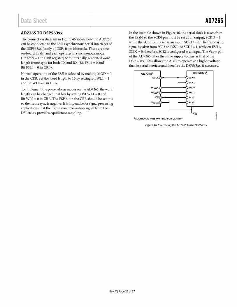
Data Sheet AD7265
Rev. C | Page 25 of 27
AD7265 TO DSP563xx The connection diagram in Figure 46 shows how the AD7265 can be connected to the ESSI (synchronous serial interface) of the DSP563xx family of DSPs from Motorola. There are two on-board ESSIs, and each operates in synchronous mode (Bit SYN = 1 in CRB register) with internally generated word length frame sync for both TX and RX (Bit FSL1 = 0 and Bit FSL0 = 0 in CRB).
Normal operation of the ESSI is selected by making MOD = 0 in the CRB. Set the word length to 16 by setting Bit WL1 = 1 and Bit WL0 = 0 in CRA.
To implement the power-down modes on the AD7265, the word length can be changed to 8 bits by setting Bit WL1 = 0 and Bit WL0 = 0 in CRA. The FSP bit in the CRB should be set to 1 so the frame sync is negative. It is imperative for signal processing applications that the frame synchronization signal from the DSP563xx provides equidistant sampling.
In the example shown in Figure 46, the serial clock is taken from the ESSI0 so the SCK0 pin must be set as an output, SCKD = 1, while the SCK1 pin is set as an input, SCKD = 0. The frame sync signal is taken from SC02 on ESSI0, so SCD2 = 1, while on ESSI1, SCD2 = 0; therefore, SC12 is configured as an input. The VDRIVE pin of the AD7265 takes the same supply voltage as that of the DSP563xx. This allows the ADC to operate at a higher voltage than its serial interface and therefore the DSP563xx, if necessary.
SCLK
DSP563xx1
1ADDITIONAL PINS OMITTED FOR CLARITY.
SCK0
SC12
SRD1
SRD0
CS
DOUTA
DOUTB
VDRIVE
VDD
SC02
SCK1
0467
4-03
9
AD72651
Figure 46. Interfacing the AD7265 to the DSP563xx
AD7265 Data Sheet
Rev. C | Page 26 of 27
APPLICATION HINTS GROUNDING AND LAYOUT The analog and digital supplies to the AD7265 are independent and separately pinned out to minimize coupling between the analog and digital sections of the device. The printed circuit board (PCB) that houses the AD7265 should be designed so that the analog and digital sections are separated and confined to certain areas of the board. This design facilitates the use of ground planes that can be easily separated.
To provide optimum shielding for ground planes, a minimum etch technique is generally best. All three AGND pins of the AD7265 should be sunk in the AGND plane. Digital and analog ground planes should be joined in only one place. If the AD7265 is in a system where multiple devices require an AGND to DGND connection, the connection should still be made at one point only, a star ground point that should be established as close as possible to the ground pins on the AD7265.
Avoid running digital lines under the device as this couples noise onto the die. However, the analog ground plane should be allowed to run under the AD7265 to avoid noise coupling. The power supply lines to the AD7265 should use as large a trace as possible to provide low impedance paths and reduce the effects of glitches on the power supply line.
To avoid radiating noise to other sections of the board, fast switching signals, such as clocks, should be shielded with digital ground, and clock signals should never run near the analog inputs. Avoid crossover of digital and analog signals. To reduce the effects of feedthrough within the board, traces on opposite sides of the board should run at right angles to each other. A microstrip technique is the best method but is not always possible with a double-sided board. In this technique, the component side of the board is dedicated to ground planes, while signals are placed on the solder side.
Good decoupling is also important. All analog supplies should be decoupled with 10 µF tantalum capacitors in parallel with 0.1 µF capacitors to GND. To achieve the best results from these decoupling components, they must be placed as close as possible to the device, ideally right up against the device. The 0.1 µF capacitors should have low effective series resistance (ESR) and effective series inductance (ESI), such as the common ceramic types or surface-mount types. These low ESR and ESI capacitors provide a low impedance path to ground at high frequencies to handle transient currents due to internal logic switching.
PCB DESIGN GUIDELINES FOR LFCSP The lands on the chip scale package (CP-32-2) are rectangular. The PCB pad for these should be 0.1 mm longer than the package land length, and 0.05 mm wider than the package land width, thereby having a portion of the pad exposed. To ensure that the solder joint size is maximized, the land should be centered on the pad.
The bottom of the chip scale package has a thermal pad. The thermal pad on the PCB should be at least as large as the exposed pad. On the PCB, there should be a clearance of at least 0.25 mm between the thermal pad and the inner edges of the pad pattern to ensure that shorting is avoided.
To improve thermal performance of the package, use thermal vias on the PCB incorporating them in the thermal pad at 1.2 mm pitch grid. The via diameter should be between 0.3 mm and 0.33 mm, and the via barrel should be plated with 1 oz. copper to plug the via. The user should connect the PCB thermal pad to AGND.
EVALUATING THE AD7265 PERFORMANCE The recommended layout for the AD7265 is outlined in the evaluation board documentation. The evaluation board package includes a fully assembled and tested evaluation board, docu-mentation, and software for controlling the board from the PC via the evaluation board controller. The evaluation board con-troller can be used in conjunction with the AD7265 evaluation board, as well as many other Analog Devices, Inc. evaluation boards ending in the CB designator, to demonstrate/evaluate the ac and dc performance of the AD7265.
The software allows the user to perform ac (fast Fourier transform) and dc (histogram of codes) tests on the AD7265. The software and documentation are on a CD shipped with the evaluation board.
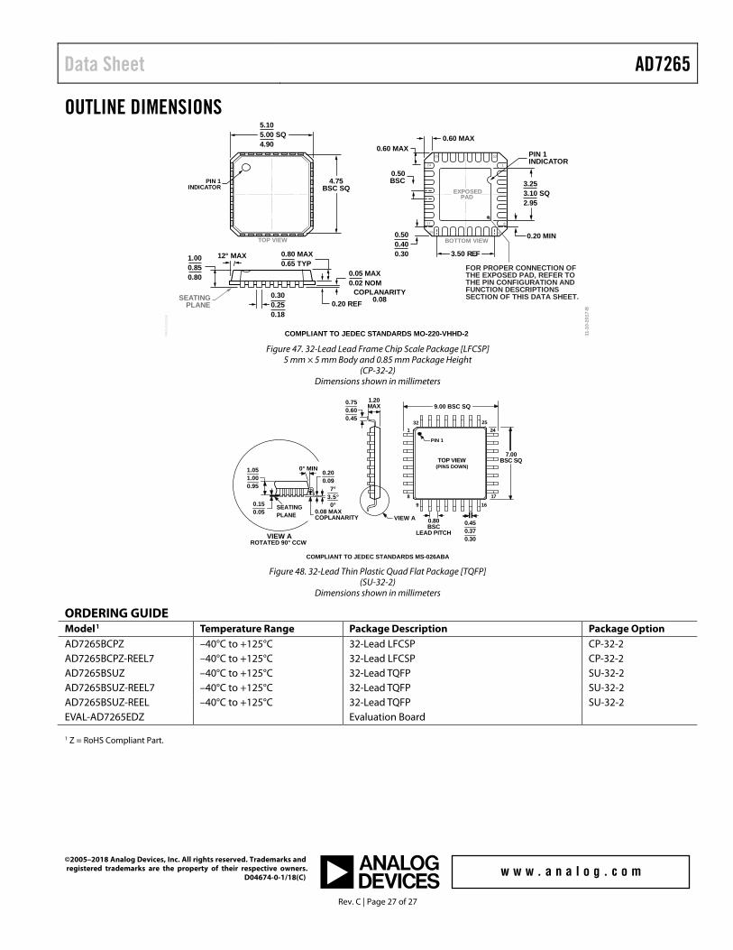
Data Sheet AD7265
Rev. C | Page 27 of 27
OUTLINE DIMENSIONS
3.253.10 SQ2.95
COMPLIANT TO JEDEC STANDARDS MO-220-VHHD-2
1
32
8
9
25
24
17
16
COPLANARITY0.08
3.50 REF
0.50BSC
PIN 1INDICATOR
PIN 1INDICATOR
0.300.250.18
0.20 REF
12° MAX 0.80 MAX0.65 TYP
1.000.850.80 0.05 MAX
0.02 NOM
0.500.400.30
4.75BSC SQ
0.60 MAX0.60 MAX
0.20 MIN
11-1
0-20
17-B
TOP VIEW
EXPOSEDPAD
BOTTOM VIEW
5.105.00 SQ4.90
SEATINGPLANE
PKG
-001
050
FOR PROPER CONNECTION OFTHE EXPOSED PAD, REFER TOTHE PIN CONFIGURATION ANDFUNCTION DESCRIPTIONSSECTION OF THIS DATA SHEET.
Figure 47. 32-Lead Lead Frame Chip Scale Package [LFCSP]
5 mm × 5 mm Body and 0.85 mm Package Height (CP-32-2)
Dimensions shown in millimeters
COMPLIANT TO JEDEC STANDARDS MS-026ABA
0.450.370.30
0.80BSC
LEAD PITCH
7.00BSC SQ
9.00 BSC SQ
1 242532
89
1716
1.20MAX0.75
0.600.45
1.051.000.95
0.200.09
0.08 MAXCOPLANARITY
SEATINGPLANE
0° MIN
7°3.5°0°0.15
0.05
VIEW AROTATED 90° CCW
VIEW A
PIN 1
TOP VIEW(PINS DOWN)
Figure 48. 32-Lead Thin Plastic Quad Flat Package [TQFP]
(SU-32-2) Dimensions shown in millimeters
ORDERING GUIDE Model1 Temperature Range Package Description Package Option AD7265BCPZ –40°C to +125°C 32-Lead LFCSP CP-32-2 AD7265BCPZ-REEL7 –40°C to +125°C 32-Lead LFCSP CP-32-2 AD7265BSUZ –40°C to +125°C 32-Lead TQFP SU-32-2 AD7265BSUZ-REEL7 –40°C to +125°C 32-Lead TQFP SU-32-2 AD7265BSUZ-REEL –40°C to +125°C 32-Lead TQFP SU-32-2 EVAL-AD7265EDZ Evaluation Board 1 Z = RoHS Compliant Part.
©2005–2018 Analog Devices, Inc. All rights reserved. Trademarks and registered trademarks are the property of their respective owners. D04674-0-1/18(C)