Embed Size (px)
Citation preview
52 Omnin
Digi® m130™
Hardware Reference Manual
90001178_B
Release date: April 2011

Omni Product Technical Specification
© 2010 Digi International Inc. 2
©2010 Digi International Inc.
All rights reserved.
Digi®, Digi International®, the Digi logo, a Digi International Company, Digi m130 are trademarks or registered trademarks of Digi International, Inc. in the United States and other countries worldwide. All other trademarks are the property of their respective owners. All other trademarks mentioned in this document are the property of their respective owners.
Information in this document is subject to change without notice and does not represent a commitment on the part of Digi International.
Digi provides this document “as is,” without warranty of any kind, either expressed or implied, including, but not limited to, the implied warranties of fitness or merchantability for a particular purpose. Digi may make improvements and/or changes in this manual or in the product(s) and/or the program(s) described in this manual at any time.
This product could include technical inaccuracies or typographical errors. Changes are periodically made to the information herein; these changes may be incorporated in new editions of the publication.
Document History
Revision Date Changes
A October 2010 Initial release
B April 2011 Detailing the DC ground characteristics in Section 3.19.1.2.3 and Table 42 in Section 3.19.1.1.3
Omni Product Technical Specification
© 2010 Digi International Inc. 3
Contents
1 About This Document .................................................................................... 8
1.1 . Documentation Updates ........................................................................................................... 8
1.2 . Contact Information ................................................................................................................. 8
1.3 . Reference Documents .............................................................................................................. 8 1.3.1 Sierra Wireless Reference Documentation ................................................................. 8 1.3.2 General Reference Documentation ............................................................................. 8
1.4 . List of Abbreviations ............................................................................................................... 9
2 General Description ..................................................................................... 12
2.1 . General Information ............................................................................................................... 12 2.1.1 RoHS Compliance .................................................................................................... 12 2.1.2 Digi m130 Features ................................................................................................... 13 2.1.3 Primary Interfaces ..................................................................................................... 13 2.1.4 Operating System ...................................................................................................... 13
2.2 . Functional Description ........................................................................................................... 14 2.2.1 GSM Functionality ................................................................................................... 15 2.2.2 Orbcomm Functionality ............................................................................................ 15 2.2.3 GPS Functionality ..................................................................................................... 15
2.3 . Operating System ................................................................................................................... 15
3 Interfaces ...................................................................................................... 16
3.1 . Antenna Connectors ............................................................................................................... 16
3.2 . System Connector .................................................................................................................. 17 3.2.1 Reference Part Numbers ........................................................................................... 17 3.2.2 Pinout ........................................................................................................................ 18
3.3 . Power Supply ......................................................................................................................... 20 3.3.1 Power Supply Description ........................................................................................ 20 3.3.2 Recommendations for Reduced Consumption .......................................................... 29
3.4 . Electrical Information for Digital I/O .................................................................................... 30
3.5 . Serial Interface ....................................................................................................................... 31 3.5.1 SPI Bus ..................................................................................................................... 31 3.5.2 I2C Bus ..................................................................................................................... 33
3.6 . Main Serial Link (UART1) .................................................................................................... 35 3.6.1 Features ..................................................................................................................... 35 3.6.2 Pin Description of UART1 Interface ........................................................................ 35
3.7 . Auxiliary Serial Link (UART2) ............................................................................................. 39 3.7.1 Features ..................................................................................................................... 39
3.8 . General Purpose Input/Output ............................................................................................... 40
3.9 . Analog to Digital Converters ................................................................................................. 41 3.9.1 Features ..................................................................................................................... 41 3.9.2 Pin Description ......................................................................................................... 41
Omni Product Technical Specification
© 2010 Digi International Inc. 4
3.10 Digital to Analog Converter ............................................................................................... 42 3.10.1 Features ..................................................................................................................... 42 3.10.2 Pin Description ......................................................................................................... 42
3.11 Analog Audio Interface ...................................................................................................... 43 3.11.1 Microphone Input ..................................................................................................... 43 3.11.2 Speaker Output Characteristics ................................................................................. 45 3.11.3 Design Recommendation .......................................................................................... 46 3.11.4 Buzzer Output ........................................................................................................... 49
3.12 PWR_ENB_N ..................................................................................................................... 51 3.12.1 Features ..................................................................................................................... 51 3.12.2 Pin Description ......................................................................................................... 51 3.12.3 Application ................................................................................................................ 51
3.13 HW_SD Signal ................................................................................................................... 54
3.14 External Interrupt ................................................................................................................ 56
3.15 BOOT Signal ...................................................................................................................... 56 3.15.1 Features ..................................................................................................................... 57 3.15.2 Pin Description ......................................................................................................... 57 3.15.3 Application ................................................................................................................ 57
3.16 VREF_2V8 Output ............................................................................................................. 58
3.17 BAT-RTC (Backup Battery) ............................................................................................... 59 3.17.1 Interface Description ................................................................................................. 59
3.18 FLASH-LED Signal ........................................................................................................... 60
3.19 RF Interface ........................................................................................................................ 61 3.19.1 RF Performance ........................................................................................................ 61
3.20 Environmental Specifications ............................................................................................. 70
3.21 Mechanical Specifications .................................................................................................. 71
3.22 Antenna Suppliers ............................................................................................................... 71
3.23 Standards and Recommendations ....................................................................................... 73
3.24 Declaration of Conformity .................................................................................................. 77
3.25 Safety Recommendations (for Information Only) .............................................................. 78 3.25.1 RF Safety .................................................................................................................. 78 3.25.2 General Safety ........................................................................................................... 79
Omni Product Technical Specification
© 2010 Digi International Inc. 5
List of Figures Figure 1: Top Level Architecture .................................................................................................................................... 14
Figure 2: Power supply during burst emission ................................................................................................................ 20
Figure 3: Connected Mode Current Waveform .............................................................................................................. 24
Figure 4: Slow Idle Mode Current Waveform ................................................................................................................ 25
Figure 5: Fast Idle Mode Current Waveform .................................................................................................................. 25
Figure 6: Transfer Mode Class 10 Current Waveform ................................................................................................... 26
Figure 7: SPI Timing diagrams, Mode 0, Master, 4 wires .............................................................................................. 32
Figure 8: I²C Timing diagrams, Master .......................................................................................................................... 34
Figure 9: Example of V24/CMOS serial link implementation for UART1 .................................................................... 37
Figure 10: Example of full modem V24/CMOS serial link implementation for UART1 .............................................. 38
Figure 11: Example of MIC input connection with LC filter ......................................................................................... 44
Figure 12: Example of MIC input connection without LC filter .................................................................................... 44
Figure 13: Example of Speaker connection .................................................................................................................... 46
Figure 14: Capacitor near Microphone ........................................................................................................................... 46
Figure 15: Audio track design ........................................................................................................................................ 48
Figure 16: Example of buzzer implementation ............................................................................................................... 50
Figure 17: Example of LED driven by the BUZZ-OUT output ..................................................................................... 50
Figure 18: Example of ON/~OFF pin connection ........................................................................................................... 51
Figure 19: Power-ON sequence (no PIN code activated) ............................................................................................... 52
Figure 20: Power-OFF sequence .................................................................................................................................... 54
Figure 21: Proper shut down sequence ........................................................................................................................... 55
Figure 22: Shut down timing diagram ............................................................................................................................ 55
Figure 23: Boot Selection Application Example ............................................................................................................ 57
Figure 24: Real Time Clock power supply ..................................................................................................................... 59
Figure 25: GPS TTFF, Hot Start Configuration ............................................................................................................. 64
Figure 26: GPS TTFF, Warm Start Configuration ......................................................................................................... 65
Figure 27: GPS TTFF, Simulator Cold Start Configuration ........................................................................................... 66
Figure 28: First Position Fix Accuracy Chart 01 ............................................................................................................ 67
Figure 29: First Position Fix Accuracy Chart 02 ............................................................................................................ 68
Figure 30: First Position Fix Accuracy Chart 03 ............................................................................................................ 69
Figure 31: Environmental classes ................................................................................................................................... 70

Omni Product Technical Specification
© 2010 Digi International Inc. 6
List of Tables Table 1: GSM /GPRS Frequency .................................................................................................................................... 15
Table 2: Antenna Connectors (Coding, Keying) ............................................................................................................. 16
Table 3: System Connector Reference Part Numbers ..................................................................................................... 17
Table 4: System connector pinout ................................................................................................................................... 19
Table 5: Power Supply Voltage ...................................................................................................................................... 20
Table 6: GSM power consumption without Open AT processing .................................................................................. 22
Table 7: Power consumption with Dhrystone benchmark Open AT application ........................................................... 23
Table 8: Power Supply Pin-out ....................................................................................................................................... 28
Table 9: CMOS Output / Input Electrical Characteristics for 2.8 volt signals ................................................................ 30
Table 10: CMOS Output / Input Electrical Characteristics for 1.8 volt signals .............................................................. 30
Table 11: Open Drain Electrical Characteristics ............................................................................................................. 30
Table 12: SPI Bus AC characteristics ............................................................................................................................. 32
Table 13: SPI Bus Configuration .................................................................................................................................... 32
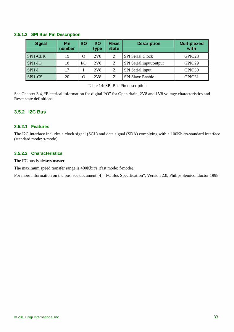
Table 14: SPI Bus Pin description .................................................................................................................................. 33
Table 15: I²C Bus AC characteristics ............................................................................................................................. 34
Table 16: IC Bus Pin Description ................................................................................................................................... 34
Table 17: UART1 Pin Description .................................................................................................................................. 35
Table 18: UART2 Pin Description .................................................................................................................................. 39
Table 19: GPIOs Pin Description ................................................................................................................................... 40
Table 20: ADCs Electrical Characteristics ..................................................................................................................... 41
Table 21: ADCs Pin Description .................................................................................................................................... 41
Table 22: DAC Electrical Characteristics ...................................................................................................................... 42
Table 23: DAC Pin Description ...................................................................................................................................... 42
Table 24: MIC2 Pin Description ..................................................................................................................................... 43
Table 25: MIC2 Electrical Characteristics ..................................................................................................................... 43
Table 26: SPK Pin Description ....................................................................................................................................... 45
Table 27: SPK Electrical Characteristics ....................................................................................................................... 45
Table 28: Audio filtering Examples with Murata Components ...................................................................................... 47
Table 29: PWM/Buzzer Output Electrical Characteristics ............................................................................................. 49
Table 30: PWM/Buzzer Output Pin Description ............................................................................................................ 49
Table 31: External Interrupt Pin description .................................................................................................................. 56
Table 32: External Interrupt Electrical Characteristics ................................................................................................... 56
Table 33: Boot Signal Mode ........................................................................................................................................... 57
Table 34: Boot Pin Description ...................................................................................................................................... 57
Table 35: VREF_2V8 Pin Description ........................................................................................................................... 58
Omni Product Technical Specification
© 2010 Digi International Inc. 7
Table 36: VREF_2V8 Electrical Characteristics ............................................................................................................ 58
Table 37: Bat-RTC Pin Description ............................................................................................................................. 59
Table 38: Bat-RTC Electrical Characteristics ................................................................................................................ 59
Table 39: Flash-LED Status ........................................................................................................................................... 60
Table 40: Flash-LED Pin Description ............................................................................................................................ 60
Table 41: Flash-LED Electrical Characteristics ............................................................................................................. 60
Table 42: GSM Antenna Specifications ......................................................................................................................... 62
Table 43: GPS Performance ........................................................................................................................................... 64
Omni Product Technical Specification
© 2010 Digi International Inc. 8
1 About This Document This document outlines the technical specifications and design integration related aspects of the Digi m130 dual-mode modem.
The Digi m130 product, formerly known as Wavecom® Q52 Omni / Sierra Wireless™ AirPrime™ Q52 Omni, is owned and sold by Digi International, Inc. All regulatory related certifications are in the process of being transferred to Digi International as part of the official product rebranding process. The product design was not modified. Customers are able to use the product based on existing certifications while the regulatory ownership transition is in progress.
1.1 Documentation Updates
Please always check the product specific section on the Digi support website at www.digiembedded.com/support for the most current revision of this guide and other product related documents.
1.2 Contact Information
For more information about Digi products, or for customer service and technical support, please contact us. World Wide Webhttp://www.digiembedded.com/support E-Mail [email protected] Telephone (U.S.)+1 952 912-3444 or (877) 912-3444 Telephone (other locations)+1 952 912-3444 References
1.3 Reference Documents
For more details, several reference documents may be consulted. The Sierra Wireless reference documents are provided in the Sierra Wireless document package, which are not authored by Digi International.
1.3.1 Sierra Wireless Reference Documentation
[1] ADL User Guide for OS v6.00 or later. Reference: WM_DEV_OAT_UGD_080
[2] DWLWin Download Application User. Guide. Reference: WM_DEV_TOO_UGD_010
[3] AT Command Interface Guide for Open AT® Firmware v7.0 or later. Reference: WM_DEV_OAT_UGD_059
1.3.2 General Reference Documentation
[4] “I²C Bus Specification”, Version 2.0, Philips Semiconductor 1998
[5] ISO 7816-3 Standard
Omni Product Technical Specification
© 2010 Digi International Inc. 9
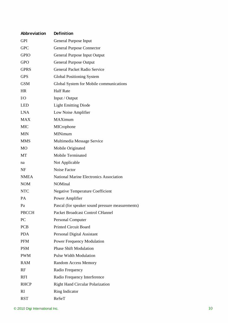
1.4 List of Abbreviations
Abbreviation Definition
AC Alternating Current
ADC Analog to Digital Converter
A/D Analog to Digital conversion
AF Audio-Frequency
AT ATtention (prefix for modem commands)
AUX AUXiliary
CAN Controller Area Network
CB Cell Broadcast
CEP Circular Error Probable
CLK CLocK
CMOS Complementary Metal Oxide Semiconductor
CS Coding Scheme
CTS Clear To Send
DAC Digital to Analog Converter
dB Decibel
DC Direct Current
DCD Data Carrier Detect
DCE Data Communication Equipment
DCS Digital Cellular System
DR Dynamic Range
DSR Data Set Ready
DTE Data Terminal Equipment
DTR Data Terminal Ready
EFR Enhanced Full Rate
E-GSM Extended GSM
EMC ElectroMagnetic Compatibility
EMI ElectroMagnetic Interference
EMS Enhanced Message Service
EN ENable
ESD ElectroStatic Discharges
FIFO First In First Out
FR Full Rate
FTA Full Type Approval
GND GrouND
Omni Product Technical Specification
© 2010 Digi International Inc. 10
Abbreviation Definition
GPI General Purpose Input
GPC General Purpose Connector
GPIO General Purpose Input Output
GPO General Purpose Output
GPRS General Packet Radio Service
GPS Global Positioning System
GSM Global System for Mobile communications
HR Half Rate
I/O Input / Output
LED Light Emitting Diode
LNA Low Noise Amplifier
MAX MAXimum
MIC MICrophone
MIN MINimum
MMS Multimedia Message Service
MO Mobile Originated
MT Mobile Terminated
na Not Applicable
NF Noise Factor
NMEA National Marine Electronics Association
NOM NOMinal
NTC Negative Temperature Coefficient
PA Power Amplifier
Pa Pascal (for speaker sound pressure measurements)
PBCCH Packet Broadcast Control CHannel
PC Personal Computer
PCB Printed Circuit Board
PDA Personal Digital Assistant
PFM Power Frequency Modulation
PSM Phase Shift Modulation
PWM Pulse Width Modulation
RAM Random Access Memory
RF Radio Frequency
RFI Radio Frequency Interference
RHCP Right Hand Circular Polarization
RI Ring Indicator
RST ReSeT
Omni Product Technical Specification
© 2010 Digi International Inc. 11
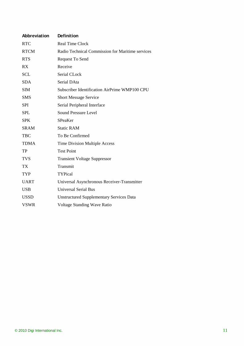
Abbreviation Definition
RTC Real Time Clock
RTCM Radio Technical Commission for Maritime services
RTS Request To Send
RX Receive
SCL Serial CLock
SDA Serial DAta
SIM Subscriber Identification AirPrime WMP100 CPU
SMS Short Message Service
SPI Serial Peripheral Interface
SPL Sound Pressure Level
SPK SPeaKer
SRAM Static RAM
TBC To Be Confirmed
TDMA Time Division Multiple Access
TP Test Point
TVS Transient Voltage Suppressor
TX Transmit
TYP TYPical
UART Universal Asynchronous Receiver-Transmitter
USB Universal Serial Bus
USSD Unstructured Supplementary Services Data
VSWR Voltage Standing Wave Ratio
Omni Product Technical Specification
© 2010 Digi International Inc. 12
2 General Description
2.1 General Information
The Digi m130 is a dual-mode GSM/Orbcomm transceiver consisting of an E-GSM/GPRS 900/1800 and 850/1900 quad-band GSM transceiver combined with a full function Orbcomm transceiver. An optional high performance GPS receiver is also available, giving a system integrator the ability to design a global coverage asset tracking device with minimal external circuitry.
A Digi m130 user always has complete control of the active communication modes and GPS receiver operations. One or both communication transceivers can be active while the AirPrime WMP100 CPU is performing continuous GPS location.
The internal ARM9 microcontroller runs a multi-tasking OS to execute all GSM functionality while transparently providing up to 80 MIPS of excess processing power for the user’s embedded firmware application. Five megabytes of flash memory and 1.5 megabytes of RAM are available for the user specific C language application code.
2.1.1 RoHS Compliance The Digi m130 is compliant with RoHS (Restriction of Hazardous Substances in Electrical and Electronic Equipment) Directive 2002/95/EC which sets limits for the use of certain restricted hazardous substances. This directive states that “from 1st July 2006, new electrical and electronic equipment put on the market does not contain lead, mercury, cadmium, hexavalent chromium, polybrominated biphenyls (PBB) or polybrominated diphenyl ethers (PBDE)”.
Omni Product Technical Specification
© 2010 Digi International Inc. 13
2.1.2 Digi m130 Features • Cellular Connectivity
o 2-Watt EGSM 900/GSM 850 radio
o 1-Watt GSM1800/1900 radio
o GPRS class 10 capable
• Satellite Connectivity
o 5-Watt Orbcomm Satellite Transceiver
o Digi ASIC Transceiver Technology
• Optional GPS Receiver
2.1.3 Primary Interfaces • Power supply
• 2*
• GSM Analog audio
UARTs Serial links
• Serial Protocol Interface (SPI)
• I2C Interface
• 2 A/D inputs and 1 D/A output
• Digital I/Os
• GSM , GPS†
2.1.4 Operating System
and Orbcomm antenna ports
• Real Time Clock with calendar
• Echo Cancellation + noise reduction (quadri codec)
• Full GSM and GPRS support
• Full Orbcomm protocol stack
• Full GPS protocol stack†
* On Digi m130 variant without GPS functionality † Depending on product variant in use
Omni Product Technical Specification
© 2010 Digi International Inc. 14
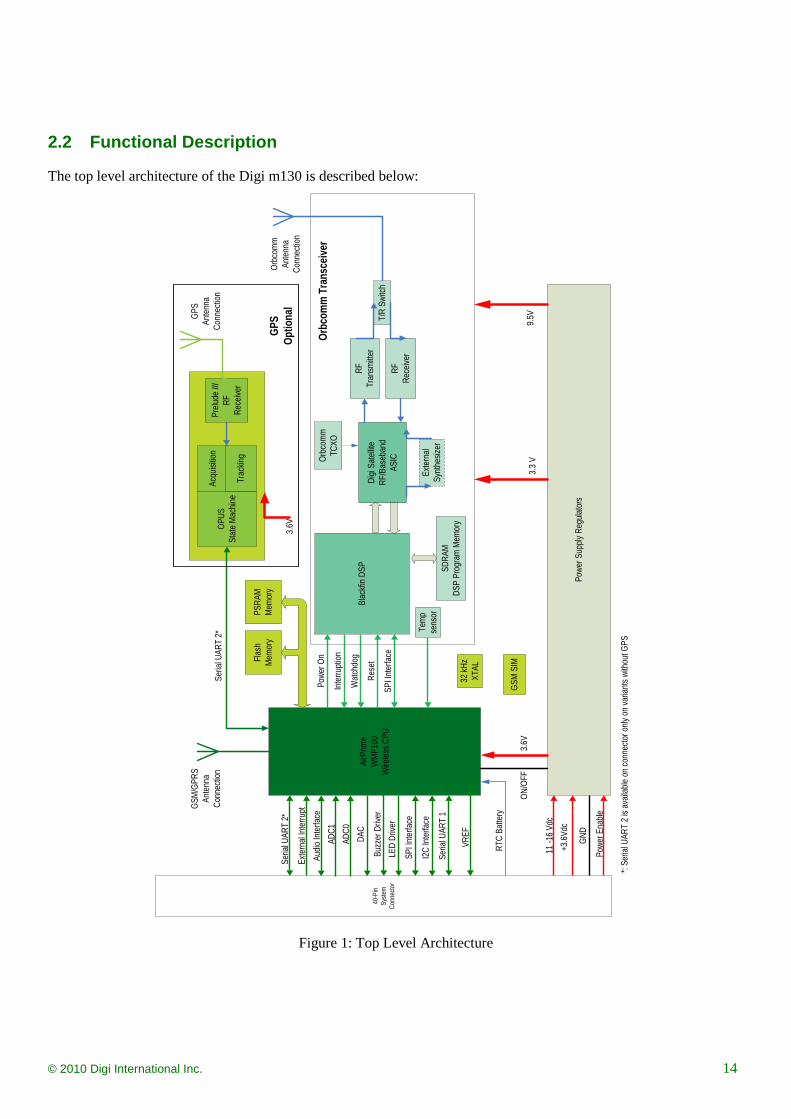
2.2 Functional Description
The top level architecture of the Digi m130 is described below:
Digi
Sate
llite
RF/B
aseb
and
ASIC
40-P
inSy
stem
Conn
ecto
r
AirP
rime
WM
P100
Wire
less C
PU
Blac
kfin
DSP SD
RAM
DSP
Prog
ram
Mem
ory
RFTr
ansm
itter
RFRe
ceive
r
T/R
Switc
h
Orbc
omm
TCXO
Exte
rnal
Synt
hesiz
er
Powe
r Sup
ply R
egula
tors
Seria
l UAR
T 1
I2C
Inte
rface
Powe
r Ena
ble
11 -1
6 Vd
c
Exte
rnal
Inte
rrupt
Seria
l UAR
T 2*
SPI I
nter
face
SPI I
nter
face
Orbc
omm
Ante
nna
Conn
ectio
n
GSM
/GPR
SAn
tenn
aCo
nnec
tion
GND
3.6V
RTC
Batte
ry
VREF
32 kH
zXT
AL
GSM
SIM
ON/O
FF
+3.6
Vdc
Tem
pse
nsor
3.3
V9.
5V
Orbc
omm
Tra
nsce
iver
LED
Drive
rBu
zzer
Driv
er
DAC
ADC0
ADC1
Audio
Inte
rface
Rese
t
Wat
chdo
g
Inte
rrupt
ion
Powe
r OnFlas
hM
emor
yPS
RAM
Mem
ory
Acqu
isitio
nOP
USSt
ate
Mac
hine
Trac
king
Prelu
de II
IRF
Re
ceive
r
Seria
l UAR
T 2*
3.6V
GPS
Ante
nna
Conn
ectio
n
GPS
Optio
nal
*: Se
rial U
ART
2 is
avail
able
on co
nnec
tor o
nly o
n va
riant
s with
out G
PS
Figure 1: Top Level Architecture
Omni Product Technical Specification
© 2010 Digi International Inc. 15
2.2.1 GSM Functionality The Radio Frequency (RF) range of the GSM transceiver complies with the Phase II EGSM 900/DCS 1800 and GSM 850/PCS 1900 recommendations. The frequencies are:
Transmit band (Tx) Receive band (Rx)
GSM 850 824 to 849 MHz 869 to 894 MHz
E-GSM 900 880 to 915 MHz 925 to 960 MHz
DCS 1800 1710 to 1785 MHz 1805 to 1880 MHz
PCS 1900 1850 to 1910 MHz 1930 to 1990 MHz
Table 1: GSM /GPRS Frequency
Voice, SMS, and GPRS data services are available either by employing the Digi m130 as a modem device connected to a user’s external processor by the UART1 link, or available through a C API to the user’s embedded Open AT software application running on the Digi m130 ARM9 microprocessor.
2.2.2 Orbcomm Functionality The Digi m130 Orbcomm transceiver provides a wide area packet switched two-way communication capability. Communication between the Digi m130 and the Orbcomm Gateway is accomplished through a constellation of low-Earth orbit satellites, orbiting approximately 500 miles above the earth.
Radio frequency communication within the Orbcomm system operates in the VHF portion of the frequency spectrum between 137 and 150 Megahertz.
Orbcomm packet data services can be accessed via a user’s external application over the UART1 link or from a user’s embedded Open AT software application running on the Digi m130 ARM9 microprocessor.
2.2.3 GPS Functionality The optional Digi m130 GPS receiver provides position location and tracking capabilities that can be accessed by an external application over a NMEA UART link or from a C API available to the user’s embedded Open ATsoftware application running on the Digi m130 ARM9 microprocessor.
2.3 Operating System
The Operating System offers an extensive set of AT commands to control both the GSM and Orbcomm functionality of the AirPrime WMP100 CPU.
The Operating System of the AirPrime WMP100 CPU is Open AT. This enables customers to implement market and application specific functionality.
Omni Product Technical Specification
© 2010 Digi International Inc. 16
3 Interfaces
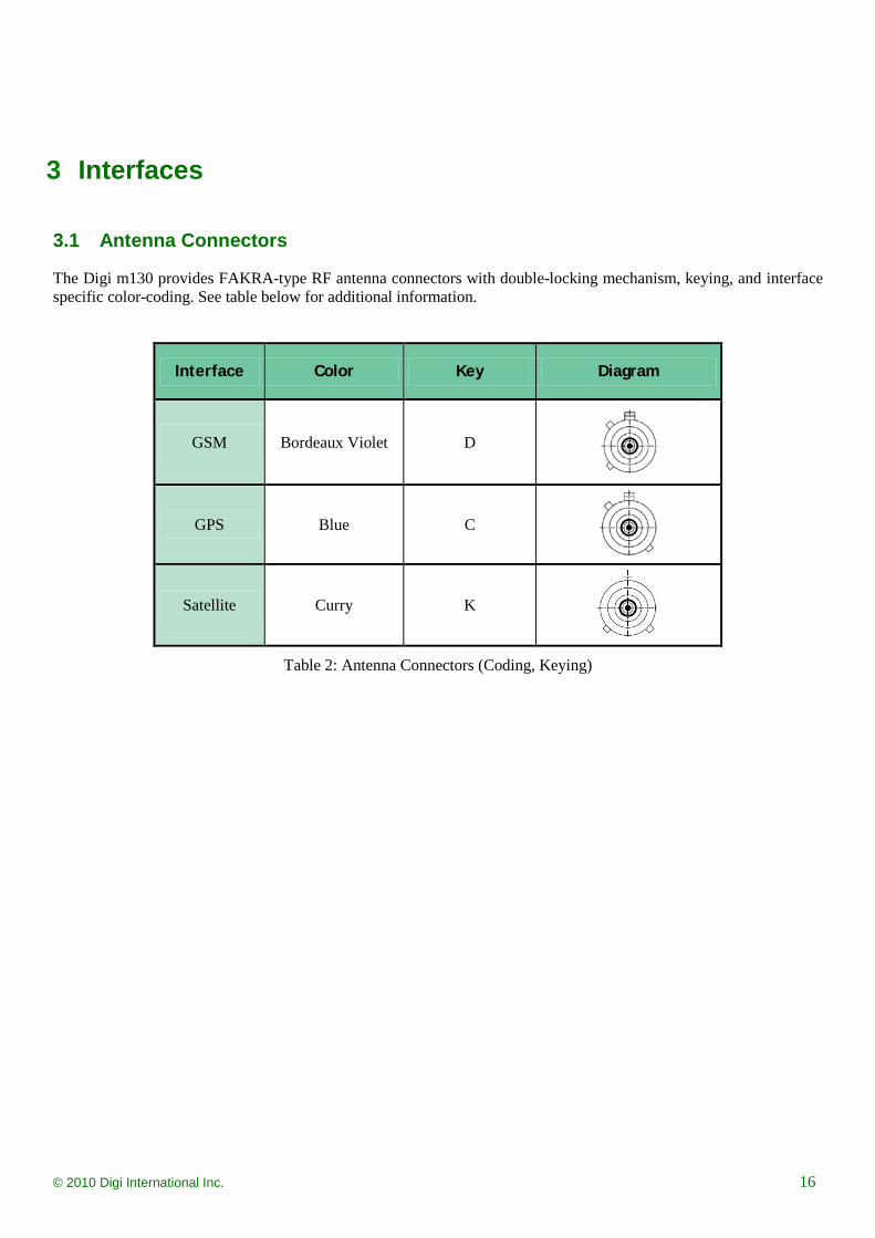
3.1 Antenna Connectors
The Digi m130 provides FAKRA-type RF antenna connectors with double-locking mechanism, keying, and interface specific color-coding. See table below for additional information.
Interface Color Key Diagram
GSM Bordeaux Violet D
GPS Blue C
Satellite Curry K
Table 2: Antenna Connectors (Coding, Keying)

Omni Product Technical Specification
© 2010 Digi International Inc. 17
3.2 System Connector
The main system connector is a keyed ODU MINI-FLAKAFIX 40-pin connector with 1.27 mm pitch.
3.2.1 Reference Part Numbers The table below provides corresponding ODU reference part numbers.
Description ODU P/N Delivery Option (nnn)
002 (Tube)
003 (Tube)
010 (Box)
050 (Tape)
System Connector 515.569.035.040.nnn 14 530
Mating Ribbon Connector
525.060.035.040.nnn 15 30
SMT Mating Header 525.041.035.040.nnn 15 400
Ribbon Cable (AWG 30) 921.659.031.040.000
Table 3: System Connector Reference Part Numbers
Please visit the ODU website at www.odu.de for detailed technical specifications as well as regional contact and order information
Omni Product Technical Specification
© 2010 Digi International Inc. 18
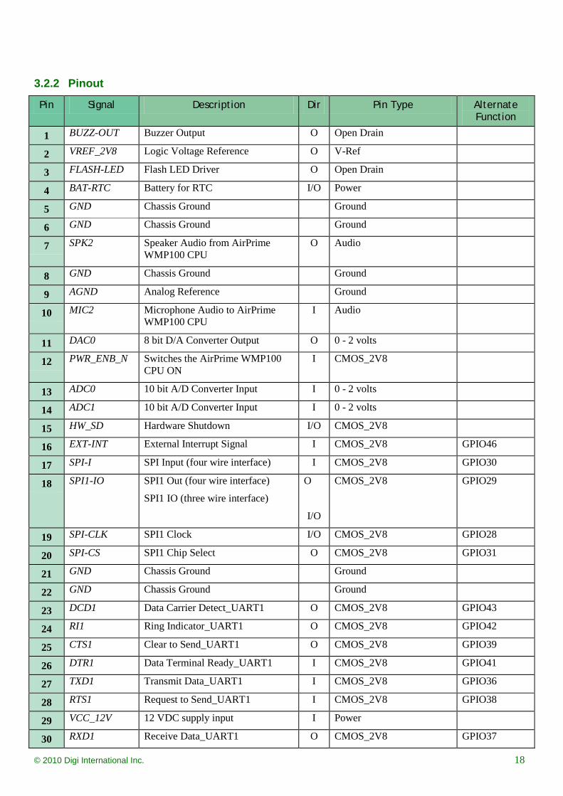
3.2.2 Pinout
Pin Signal Description Dir Pin Type Alternate Function
1 BUZZ-OUT Buzzer Output O Open Drain
2 VREF_2V8 Logic Voltage Reference O V-Ref
3 FLASH-LED Flash LED Driver O Open Drain
4 BAT-RTC Battery for RTC I/O Power
5 GND Chassis Ground Ground
6 GND Chassis Ground Ground
7 SPK2 Speaker Audio from AirPrime WMP100 CPU
O Audio
8 GND Chassis Ground Ground
9 AGND Analog Reference Ground
10 MIC2 Microphone Audio to AirPrime WMP100 CPU
I Audio
11 DAC0 8 bit D/A Converter Output O 0 - 2 volts
12 PWR_ENB_N Switches the AirPrime WMP100 CPU ON
I CMOS_2V8
13 ADC0 10 bit A/D Converter Input I 0 - 2 volts
14 ADC1 10 bit A/D Converter Input I 0 - 2 volts
15 HW_SD Hardware Shutdown I/O CMOS_2V8
16 EXT-INT External Interrupt Signal I CMOS_2V8 GPIO46
17 SPI-I SPI Input (four wire interface) I CMOS_2V8 GPIO30
18 SPI1-IO SPI1 Out (four wire interface)
SPI1 IO (three wire interface)
O
I/O
CMOS_2V8
GPIO29
19 SPI-CLK SPI1 Clock I/O CMOS_2V8 GPIO28
20 SPI-CS SPI1 Chip Select O CMOS_2V8 GPIO31
21 GND Chassis Ground Ground
22 GND Chassis Ground Ground
23 DCD1 Data Carrier Detect_UART1 O CMOS_2V8 GPIO43
24 RI1 Ring Indicator_UART1 O CMOS_2V8 GPIO42
25 CTS1 Clear to Send_UART1 O CMOS_2V8 GPIO39
26 DTR1 Data Terminal Ready_UART1 I CMOS_2V8 GPIO41
27 TXD1 Transmit Data_UART1 I CMOS_2V8 GPIO36
28 RTS1 Request to Send_UART1 I CMOS_2V8 GPIO38
29 VCC_12V 12 VDC supply input I Power
30 RXD1 Receive Data_UART1 O CMOS_2V8 GPIO37
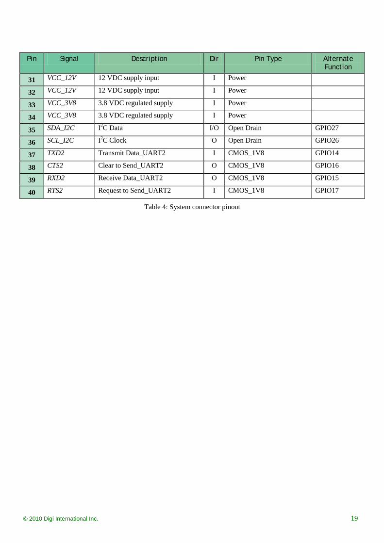
Omni Product Technical Specification
© 2010 Digi International Inc. 19
Pin Signal Description Dir Pin Type Alternate Function
31 VCC_12V 12 VDC supply input I Power
32 VCC_12V 12 VDC supply input I Power
33 VCC_3V8 3.8 VDC regulated supply I Power
34 VCC_3V8 3.8 VDC regulated supply I Power
35 SDA_I2C I2C Data I/O Open Drain GPIO27
36 SCL_I2C I2C Clock O Open Drain GPIO26
37 TXD2 Transmit Data_UART2 I CMOS_1V8 GPIO14
38 CTS2 Clear to Send_UART2 O CMOS_1V8 GPIO16
39 RXD2 Receive Data_UART2 O CMOS_1V8 GPIO15
40 RTS2 Request to Send_UART2 I CMOS_1V8 GPIO17
Table 4: System connector pinout
Omni Product Technical Specification
© 2010 Digi International Inc. 20
3.3 Power Supply
3.3.1 Power Supply Description The power supply required for the Digi m130 is a dual rail supply; VCC_3V8 and VCC_12V. VCC_12V is only required to support Orbcomm mode operation. VCC_3V8 is used for GSM/GPRS, Orbcomm and GPS operation.
The power supply is one of the key issues in the design of a dual mode terminal. Getting full performance from the AirPrime WMP100 CPU requires particularly careful attention to the ability of the power supplies to provide clean DC power.
Due to the burst emission modes used in GSM/GPRS, and Orbcomm communication, the VCC_3V8 and VCC_12V8 power supplies must be able to deliver high current peaks in a short time. During the peaks, the ripple (Uripp) on these supply voltages must not exceed a certain limit (see Table 5: Power Supply Voltage).
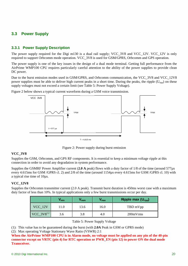
Figure 2 below shows a typical current waveform during a GSM voice transmission.
Uripp
VCC 3V8
Uripp
T = 4,615 ms
t = 577 µs
Figure 2: Power supply during burst emission
VCC_3V8 Supplies the GSM, Orbcomm, and GPS RF components. It is essential to keep a minimum voltage ripple at this connection in order to avoid any degradation in system performance.
Supplies the GSMRF Power Amplifier current (2.0 A peak) flows with a duty factor of 1/8 of the time (around 577µs every 4.615ms for GSM /GPRS cl. 2) and 2/8 of the time (around 1154µs every 4.615ms for GSM /GPRS cl. 10) with a typical rise time of 10µs.
VCC_12V8 Supplies the Orbcomm transmitter current (2.0 A peak). Transmit burst duration is 450ms worst case with a maximum duty factor of less than 10%. In typical applications only a few burst transmissions occur per day.
Vmin Vnom Vmax Ripple max (Uripp)
VCC_12V 11.0 13.6 16.0 TBD mVpp
VCC_3V81,2 3.6 3.8 4.0 200mVrms
Table 5: Power Supply Voltage
(1): This value has to be guaranteed during the burst (with 2.0A Peak in GSM or GPRS mode) (2): Max operating Voltage Stationary Wave Ratio (VSWR) 2:1 When the AirPrime WMP100 CPU is in Alarm mode, no voltage must be applied on any pin of the 40-pin connector except on VRTC (pin 4) for RTC operation or PWR_EN (pin 12) to power ON the dual mode Transceiver.

Omni Product Technical Specification
© 2010 Digi International Inc. 21
When supplying the Digi m130 with power through a battery, the total impedance (battery+protections+PCB) on 3V8 should be <150 mOhms.
3.3.1.1 Power Consumption Power consumption estimates for the Digi m130 are relatively complex due to the multimode capability of the AirPrime WMP100 CPU. The instantaneous power consumption is dependent on the following factors:
• The specific operating mode of each active function
o GSM/GPRS – Off, Alarm mode, Fast Idle mode, Slow Idle mode , or Transmit mode o Orbcomm – Off, Receive mode, or Transmit mode o GPS – Off, GPS Acquisition mode or GPS Tracking mode o Open AT application – Idle or executing max instructions/sec
• The frequency band being used for GSM communication (850/900 or 1800/1900 MHz).
• The transmit output power required during a GSM RX/TX connection depending on the distance to the nearest available GSM base station.
• The data transfer rate during a GSM/GPRS or Orbcomm connection to the network
The ARM9 microprocessor and its GSM/GPRS transceiver are a key component of the Digi m130. This section begins with an explanation of its primary GSM operating modes and significant details on the power consumption in each mode.
The microprocessor can be in one of four operational modes:
• Alarm Mode – This is the lowest power mode available. The only circuitry running is the internal hardware timer which can be configured to wake the Digi m130 microprocessor after a designated amount of time. No communication capabilities, GPS location, or microprocessor I/O functions are available in this mode.
• Fast Idle Mode – Full Receiver functionality of the GSM/GPRS transceiver is available in this mode. All microprocessor I/O functions are available and the microprocessor can be communicating with the GPS and Orbcomm transceiver functions.
• Slow Idle Mode – This is a power saving GSM/GPRS receive mode where the microprocessor is running on a 32 KHz clock. The GSM/GPRS receiver regularly checks for incoming voice/data traffic but most microprocessor I/O functions are disabled and all Open AT processing must be in an idle state. If any incoming GSM/GPRS traffic is available, an external interrupt occurs, or the UART1 DSR line becomes active, the processor switches into Fast Idle Mode before processing the request.
• Transmit Mode – Two transmit sub-modes are listed in the following table; Connected (Voice) mode and Transfer mode when GPRS data is being transmitted over the network
Table 4 and 5 below list the VCC_3V8 power supply current for each GSM/GPRS mode, RF band, transmit power level, and the amount of Open AT processing activity. Additional power supply current required for Orbcomm and GPS modes of operation must be added to these numbers and will be discussed later
Omni Product Technical Specification
© 2010 Digi International Inc. 22
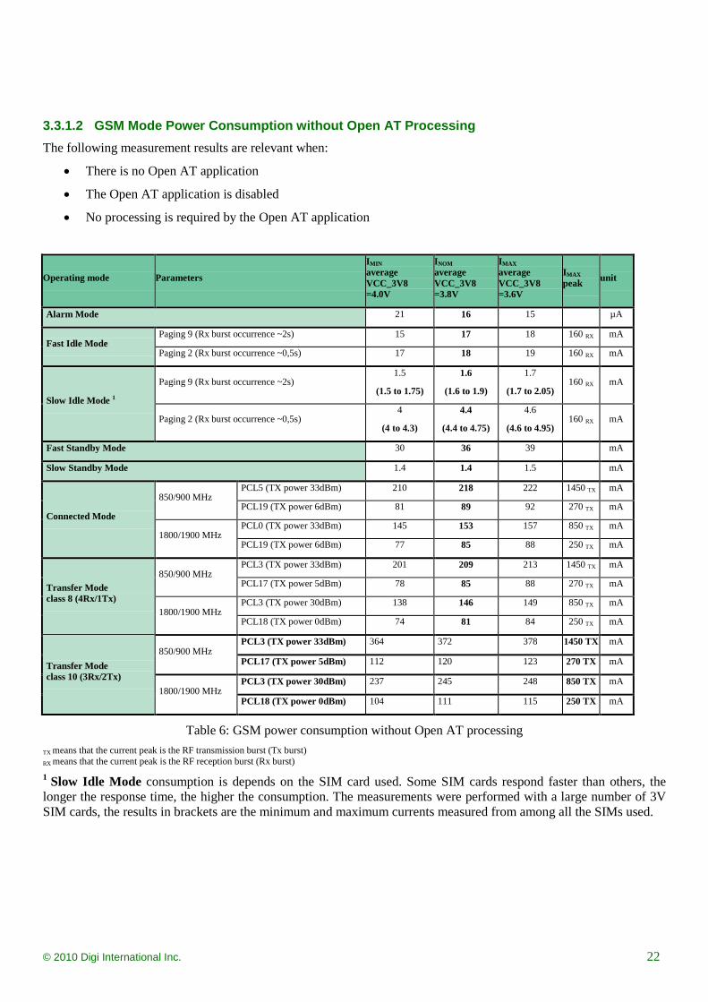
3.3.1.2 GSM Mode Power Consumption without Open AT Processing The following measurement results are relevant when:
• There is no Open AT application
• The Open AT application is disabled
• No processing is required by the Open AT application
Operating mode Parameters
IMIN average VCC_3V8 =4.0V
INOM average VCC_3V8 =3.8V
IMAX average VCC_3V8 =3.6V
IMAX peak unit
Alarm Mode 21 16 15 µA
Fast Idle Mode Paging 9 (Rx burst occurrence ~2s) 15 17 18 160 RX mA
Paging 2 (Rx burst occurrence ~0,5s) 17 18 19 160 RX mA
Slow Idle Mode 1
Paging 9 (Rx burst occurrence ~2s) 1.5
(1.5 to 1.75)
1.6
(1.6 to 1.9)
1.7
(1.7 to 2.05) 160 RX mA
Paging 2 (Rx burst occurrence ~0,5s) 4
(4 to 4.3)
4.4
(4.4 to 4.75)
4.6
(4.6 to 4.95) 160 RX mA
Fast Standby Mode 30 36 39 mA
Slow Standby Mode 1.4 1.4 1.5 mA
Connected Mode
850/900 MHz PCL5 (TX power 33dBm) 210 218 222 1450 TX mA
PCL19 (TX power 6dBm) 81 89 92 270 TX mA
1800/1900 MHz PCL0 (TX power 33dBm) 145 153 157 850 TX mA
PCL19 (TX power 6dBm) 77 85 88 250 TX mA
Transfer Mode class 8 (4Rx/1Tx)
850/900 MHz PCL3 (TX power 33dBm) 201 209 213 1450 TX mA
PCL17 (TX power 5dBm) 78 85 88 270 TX mA
1800/1900 MHz PCL3 (TX power 30dBm) 138 146 149 850 TX mA
PCL18 (TX power 0dBm) 74 81 84 250 TX mA
Transfer Mode class 10 (3Rx/2Tx)
850/900 MHz PCL3 (TX power 33dBm) 364 372 378 1450 TX mA
PCL17 (TX power 5dBm) 112 120 123 270 TX mA
1800/1900 MHz PCL3 (TX power 30dBm) 237 245 248 850 TX mA
PCL18 (TX power 0dBm) 104 111 115 250 TX mA
Table 6: GSM power consumption without Open AT processing TX means that the current peak is the RF transmission burst (Tx burst)
RX means that the current peak is the RF reception burst (Rx burst) 1 Slow Idle Mode consumption is depends on the SIM card used. Some SIM cards respond faster than others, the longer the response time, the higher the consumption. The measurements were performed with a large number of 3V SIM cards, the results in brackets are the minimum and maximum currents measured from among all the SIMs used.
Omni Product Technical Specification
© 2010 Digi International Inc. 23
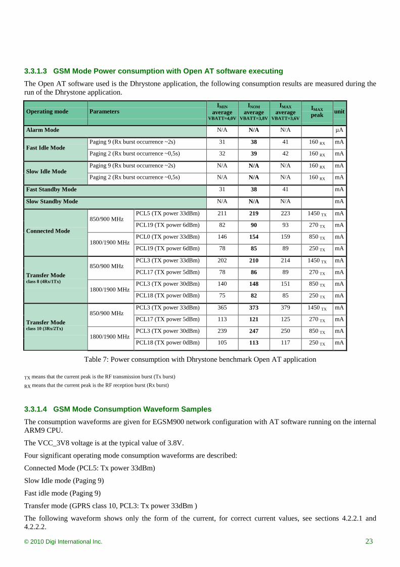
3.3.1.3 GSM Mode Power consumption with Open AT software executing The Open AT software used is the Dhrystone application, the following consumption results are measured during the run of the Dhrystone application.
Operating mode Parameters IMIN
average VBATT=4,0V
INOM average
VBATT=3,8V
IMAX average
VBATT=3,6V IMAX peak unit
Alarm Mode N/A N/A N/A µA
Fast Idle Mode Paging 9 (Rx burst occurrence ~2s) 31 38 41 160 RX mA
Paging 2 (Rx burst occurrence ~0,5s) 32 39 42 160 RX mA
Slow Idle Mode Paging 9 (Rx burst occurrence ~2s) N/A N/A N/A 160 RX mA
Paging 2 (Rx burst occurrence ~0,5s) N/A N/A N/A 160 RX mA
Fast Standby Mode 31 38 41 mA
Slow Standby Mode N/A N/A N/A mA
Connected Mode
850/900 MHz PCL5 (TX power 33dBm) 211 219 223 1450 TX mA
PCL19 (TX power 6dBm) 82 90 93 270 TX mA
1800/1900 MHz PCL0 (TX power 33dBm) 146 154 159 850 TX mA
PCL19 (TX power 6dBm) 78 85 89 250 TX mA
Transfer Mode class 8 (4Rx/1Tx)
850/900 MHz PCL3 (TX power 33dBm) 202 210 214 1450 TX mA
PCL17 (TX power 5dBm) 78 86 89 270 TX mA
1800/1900 MHz PCL3 (TX power 30dBm) 140 148 151 850 TX mA
PCL18 (TX power 0dBm) 75 82 85 250 TX mA
Transfer Mode class 10 (3Rx/2Tx)
850/900 MHz PCL3 (TX power 33dBm) 365 373 379 1450 TX mA
PCL17 (TX power 5dBm) 113 121 125 270 TX mA
1800/1900 MHz PCL3 (TX power 30dBm) 239 247 250 850 TX mA
PCL18 (TX power 0dBm) 105 113 117 250 TX mA
Table 7: Power consumption with Dhrystone benchmark Open AT application
TX means that the current peak is the RF transmission burst (Tx burst) RX means that the current peak is the RF reception burst (Rx burst)
3.3.1.4 GSM Mode Consumption Waveform Samples The consumption waveforms are given for EGSM900 network configuration with AT software running on the internal ARM9 CPU.
The VCC_3V8 voltage is at the typical value of 3.8V.
Four significant operating mode consumption waveforms are described:
Connected Mode (PCL5: Tx power 33dBm)
Slow Idle mode (Paging 9)
Fast idle mode (Paging 9)
Transfer mode (GPRS class 10, PCL3: Tx power 33dBm )
The following waveform shows only the form of the current, for correct current values, see sections 4.2.2.1 and 4.2.2.2.
Omni Product Technical Specification
© 2010 Digi International Inc. 24
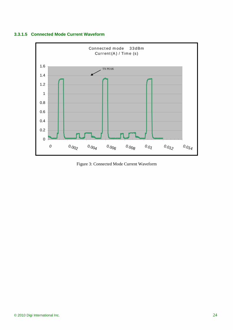
3.3.1.5 Connected Mode Current Waveform
Connec t ed m ode 3 3 dBmCur r ent (A ) / Ti m e (s)
0
0.2
0.4
0.6
0.8
1
1.2
1.4
1.6
0 0.002 0.004 0.006 0.008 0.01 0.012 0.014
Figure 3: Connected Mode Current Waveform
TX PEAK
Omni Product Technical Specification
© 2010 Digi International Inc. 25
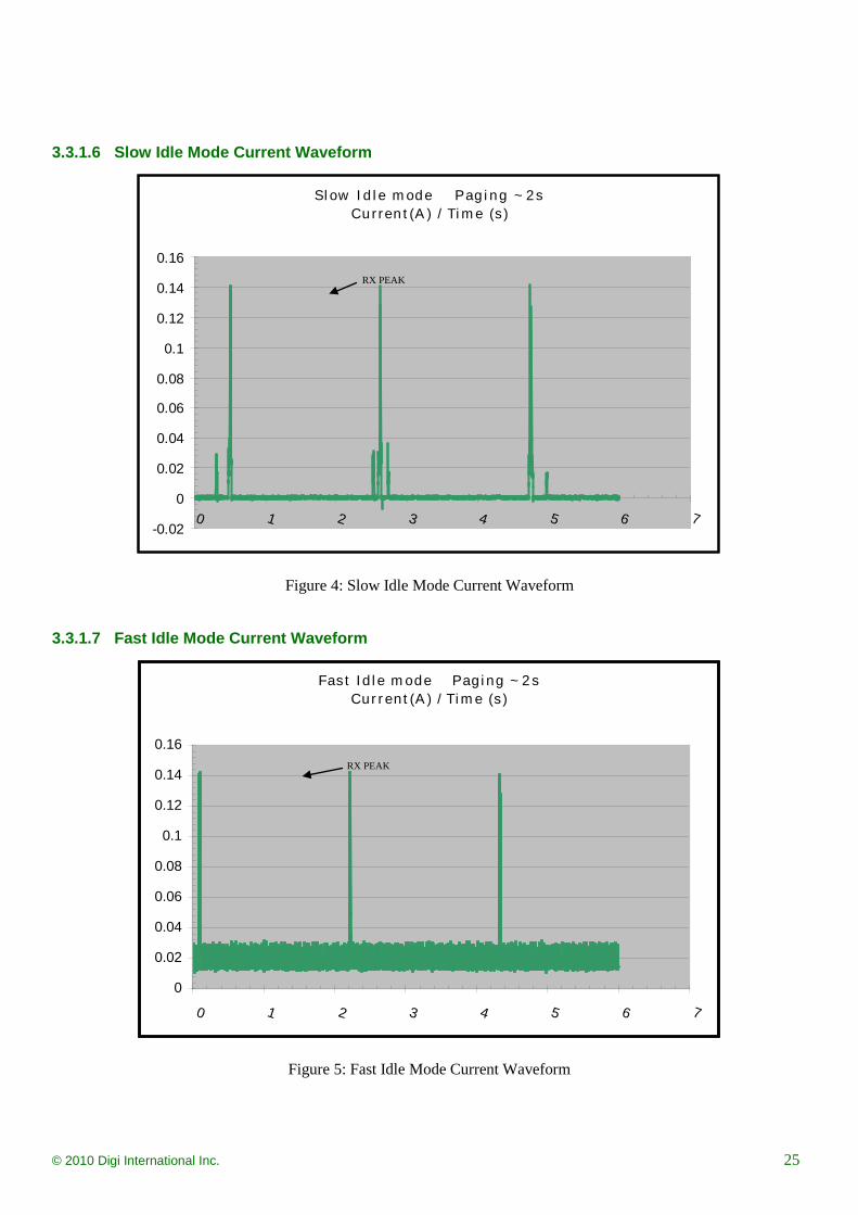
3.3.1.6 Slow Idle Mode Current Waveform
Sl ow I d l e m ode Pag i ng ~ 2sCur ren t (A ) / Ti m e (s)
-0.02
0
0.02
0.04
0.06
0.08
0.1
0.12
0.14
0.16
0 1 2 3 4 5 6 7
Figure 4: Slow Idle Mode Current Waveform
3.3.1.7 Fast Idle Mode Current Waveform
Fast I d l e m ode Pag i ng ~ 2 sCur r ent (A ) / Ti m e (s)
0
0.02
0.04
0.06
0.08
0.1
0.12
0.14
0.16
0 1 2 3 4 5 6 7
Figure 5: Fast Idle Mode Current Waveform
RX PEAK
RX PEAK
Omni Product Technical Specification
© 2010 Digi International Inc. 26
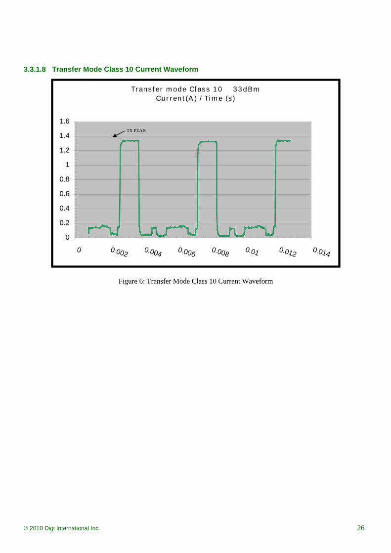
3.3.1.8 Transfer Mode Class 10 Current Waveform
Tr ansf er m ode Cl ass 1 0 3 3 dBmCur r en t (A ) / Ti m e (s)
0
0.2
0.4
0.6
0.8
1
1.2
1.4
1.6
0 0.002 0.004 0.006 0.008 0.01 0.012 0.014
Figure 6: Transfer Mode Class 10 Current Waveform
TX PEAK
Omni Product Technical Specification
© 2010 Digi International Inc. 27
3.3.1.9 Orbcomm Transceiver Power Consumption While turned on, the Orbcomm transceiver portion of the Digi m130 draws current from both the VCC_3V8 and VCC_12V power supply rails. The Digi m130 ARM9 microprocessor must be operating in either Fast Idle or Fast Standby mode while the Orbcomm Transceiver is turned on.
Operating mode Power Supply Rail IMAX unit
Orbcomm RX Mode VCC_3V8 (nominal voltage) 250 mA
VCC_12V (nominal voltage) 20 mA
Orbcomm TX Mode VCC_3V8 (nominal voltage) 250 mA
VCC_12V (nominal voltage) 1900 mA
The values in the above table only include the Orbcomm transceiver current requirements and 38 mA of VCC_3V8 current to account for the ARM9 Processor being in Fast Idle mode. Please be aware the VCC_3V8 power supply rail may also be simultaneously supplying current to the GSM/GPRS transmitter and the Digi m130 GPS receiver (if turned on).
3.3.1.10 GPS Receiver Power Consumption While turned on, the GPS receiver portion of the Digi m130 draws current from the VCC_3V8 power supply rail.
Operating mode Power Supply Rail IMAX unit
Standby Mode VCC_3V8 (nominal voltage) 15 mA
Acquisition Mode VCC_3V8 (nominal voltage) 45 mA
Outdoor Tracking Mode VCC_3V8 (nominal voltage) 35 mA
Indoor Tracking Mode VCC_3V8 (nominal voltage) 40 mA
The values in the above table only include the GPS receiver current requirements and 30 mA of VCC_3V8 current to account for the ARM9 Processor being in Fast Idle mode. Please be aware the VCC_3V8 power supply rail may also be simultaneously supplying current to the GSM/GPRS transmitter and the Digi m130 Orbcomm transceiver (if turned on).
Omni Product Technical Specification
© 2010 Digi International Inc. 28
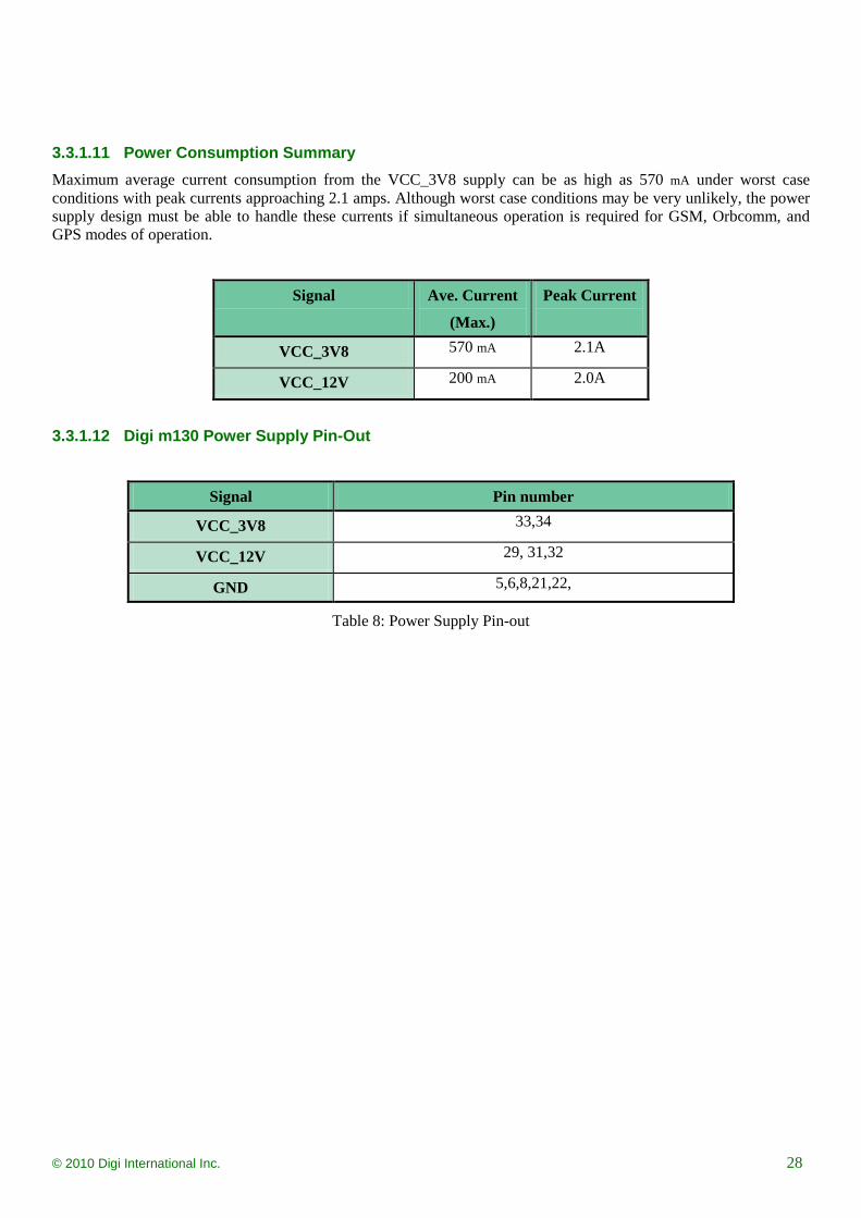
3.3.1.11 Power Consumption Summary Maximum average current consumption from the VCC_3V8 supply can be as high as 570 mA under worst case conditions with peak currents approaching 2.1 amps. Although worst case conditions may be very unlikely, the power supply design must be able to handle these currents if simultaneous operation is required for GSM, Orbcomm, and GPS modes of operation.
Signal Ave. Current
(Max.)
Peak Current
VCC_3V8 570 mA 2.1A
VCC_12V 200 mA 2.0A
3.3.1.12 Digi m130 Power Supply Pin-Out
Signal Pin number
VCC_3V8 33,34
VCC_12V 29, 31,32
GND 5,6,8,21,22,
Table 8: Power Supply Pin-out
Omni Product Technical Specification
© 2010 Digi International Inc. 29
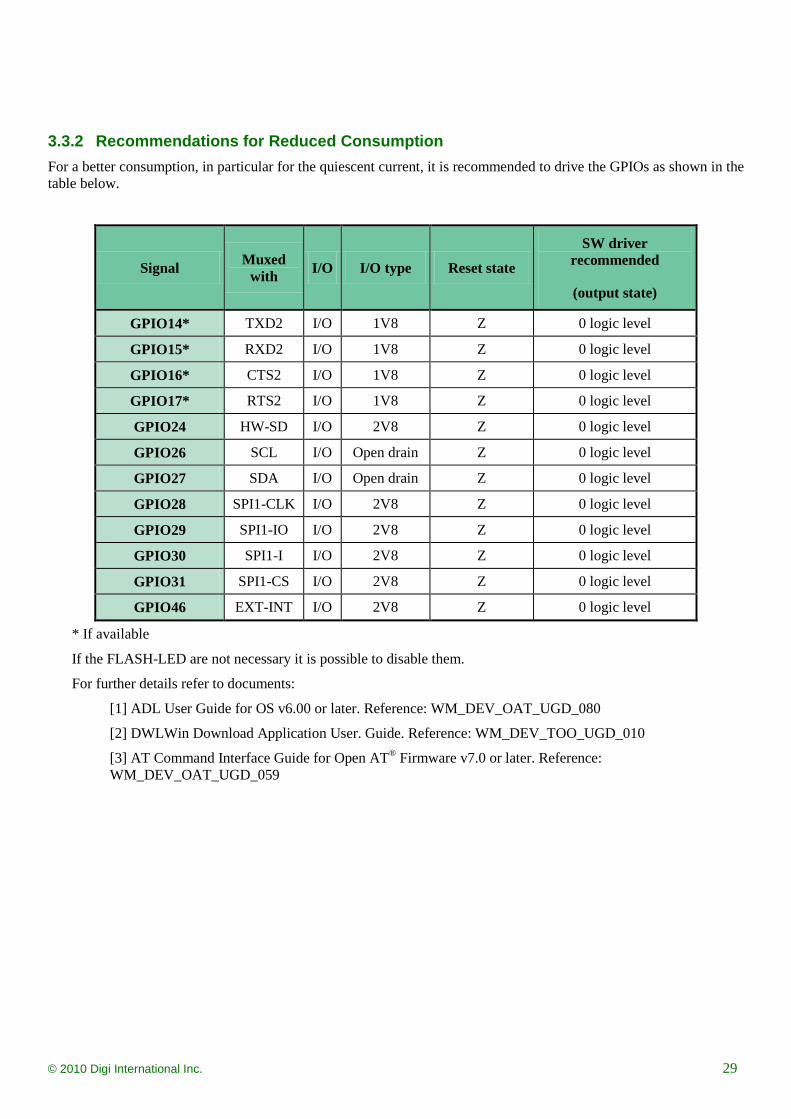
3.3.2 Recommendations for Reduced Consumption For a better consumption, in particular for the quiescent current, it is recommended to drive the GPIOs as shown in the table below.
Signal Muxed with I/O I/O type Reset state
SW driver recommended
(output state)
GPIO14* TXD2 I/O 1V8 Z 0 logic level
GPIO15* RXD2 I/O 1V8 Z 0 logic level
GPIO16* CTS2 I/O 1V8 Z 0 logic level
GPIO17* RTS2 I/O 1V8 Z 0 logic level
GPIO24 HW-SD I/O 2V8 Z 0 logic level
GPIO26 SCL I/O Open drain Z 0 logic level
GPIO27 SDA I/O Open drain Z 0 logic level
GPIO28 SPI1-CLK I/O 2V8 Z 0 logic level
GPIO29 SPI1-IO I/O 2V8 Z 0 logic level
GPIO30 SPI1-I I/O 2V8 Z 0 logic level
GPIO31 SPI1-CS I/O 2V8 Z 0 logic level
GPIO46 EXT-INT I/O 2V8 Z 0 logic level
* If available
If the FLASH-LED are not necessary it is possible to disable them.
For further details refer to documents:
[1] ADL User Guide for OS v6.00 or later. Reference: WM_DEV_OAT_UGD_080
[2] DWLWin Download Application User. Guide. Reference: WM_DEV_TOO_UGD_010
[3] AT Command Interface Guide for Open AT® Firmware v7.0 or later. Reference: WM_DEV_OAT_UGD_059

Omni Product Technical Specification
© 2010 Digi International Inc. 30
3.4 Electrical Information for Digital I/O
The CMOS signals of the Digi m130 shall only be considered valid when the level of the VREF_2V8 signal is above 2.4V.
Parameters for CMOS_2V8 Signals
(Nominal voltage level is 2.8V) Test
Conditions Limits
Units Min Max
High level output voltage (IOH = 4mA) VOH 2.4 Volts
Low level output voltage (IOL = -4mA) VOL 0.4 Volts High level input voltage (IIH = 60 µA) VIH 1.96 3.2* Volts
Low level input voltage (IIL = 60 µA) VIL -0.5* 0.84 Volts
Table 9: CMOS Output / Input Electrical Characteristics for 2.8 volt signals
Parameters for CMOS_1V8 Signals
(Nominal voltage level is 1.8V) Test
Conditions Limits
Units Min Max
High level output voltage
(IOH= 4mA) VOH 1.4 Volts
Low level output voltage
(IOL = -4mA) VOL 0.4 Volts
High level input voltage (IIH = 60 µA) VIH 1.33 2.2* Volts Low level input voltage (IIL = 60 µA) VIL -0.5* 0.54 Volts
Table 10: CMOS Output / Input Electrical Characteristics for 1.8 volt signals
Parameters for Open Drain Signals Parameter Limits
Min Max
FLASH-LED VOH 0.4V IOL 8mA
BUZZ_OUT VOL 0.4V IOL 100mA
SDA/GPIO27 and SCL/GPIO26
VTOLERATED 3.3V VIH 2.0V VIL 0.8V VOL 0.4V IOL 3mA
Table 11: Open Drain Electrical Characteristics
* Absolute Maximum Ratings
Omni Product Technical Specification
© 2010 Digi International Inc. 31
3.5 Serial Interface
3.5.1 SPI Bus The SPI bus interface includes:
• A Clock signal
• A SPI Data output or SPI Data Input/Output signal depending on whether 4 or 3 wires SPI interface is selected
• A SPI Data Input signal for applications using 4 wires interface
• A SPI Chip Select signal
• SPI bus characteristics:
• Master mode operation
• SPI speed is from 101.5 Kbit/s to 13 Mbit/s in master mode operation
• 3 or 4-wire interface
• SPI-mode configuration: 0 to 3
• 1 to 16 bits data length
Omni Product Technical Specification
© 2010 Digi International Inc. 32
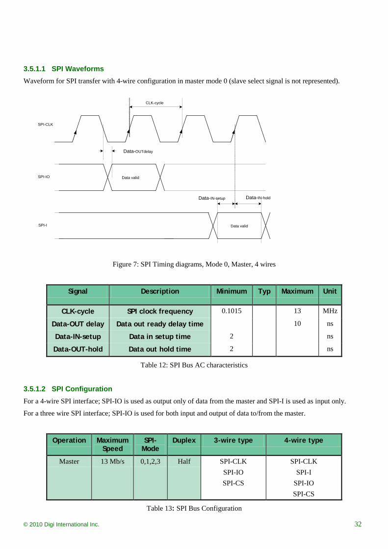
3.5.1.1 SPI Waveforms Waveform for SPI transfer with 4-wire configuration in master mode 0 (slave select signal is not represented).
Data-OUTdelay
CLK-cycle
Data-IN-holdData-IN-setup
Data valid
Data valid
SPI-CLK
SPI-IO
SPI-I
Figure 7: SPI Timing diagrams, Mode 0, Master, 4 wires
Signal Description Minimum Typ Maximum Unit
CLK-cycle SPI clock frequency 0.1015 13 MHz
Data-OUT delay Data out ready delay time 10 ns
Data-IN-setup Data in setup time 2 ns
Data-OUT-hold Data out hold time 2 ns
Table 12: SPI Bus AC characteristics
3.5.1.2 SPI Configuration For a 4-wire SPI interface; SPI-IO is used as output only of data from the master and SPI-I is used as input only.
For a three wire SPI interface; SPI-IO is used for both input and output of data to/from the master.
Operation Maximum Speed
SPI-Mode
Duplex 3-wire type 4-wire type
Master 13 Mb/s 0,1,2,3 Half SPI-CLK SPI-IO SPI-CS
SPI-CLK SPI-I
SPI-IO SPI-CS
Table 13: SPI Bus Configuration
Omni Product Technical Specification
© 2010 Digi International Inc. 33
3.5.1.3 SPI Bus Pin Description
Signal Pin number
I/O I/O type
Reset state
Description Multiplexed with
SPI1-CLK 19 O 2V8 Z SPI Serial Clock GPIO28 SPI1-IO 18 I/O 2V8 Z SPI Serial input/output GPIO29 SPI1-I 17 I 2V8 Z SPI Serial input GPIO30 SPI1-CS 20 O 2V8 Z SPI Slave Enable GPIO31
Table 14: SPI Bus Pin description
See Chapter 3.4, “Electrical information for digital I/O” for Open drain, 2V8 and 1V8 voltage characteristics and Reset state definitions.
3.5.2 I2C Bus
3.5.2.1 Features The I2C interface includes a clock signal (SCL) and data signal (SDA) complying with a 100Kbit/s-standard interface (standard mode: s-mode).
3.5.2.2 Characteristics The I²C bus is always master.
The maximum speed transfer range is 400Kbit/s (fast mode: f-mode).
For more information on the bus, see document [4] “I²C Bus Specification”, Version 2.0, Philips Semiconductor 1998
Omni Product Technical Specification
© 2010 Digi International Inc. 34
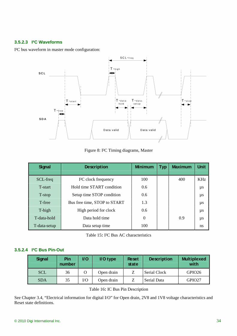
3.5.2.3 I²C Waveforms I²C bus waveform in master mode configuration:
D at a v alid
S C L
S D A
D at a v alid
T - f r e e
T - s t a r t
T - h ig h
T - d a t a -s e t u p
T - d a t a -h o ld
T - s t o p
S C L- f r e q
Figure 8: I²C Timing diagrams, Master
Signal Description Minimum Typ Maximum Unit
SCL-freq I²C clock frequency 100 400 KHz
T-start Hold time START condition 0.6 µs
T-stop Setup time STOP condition 0.6 µs
T-free Bus free time, STOP to START 1.3 µs
T-high High period for clock 0.6 µs
T-data-hold Data hold time 0 0.9 µs
T-data-setup Data setup time 100 ns
Table 15: I²C Bus AC characteristics
3.5.2.4 I²C Bus Pin-Out
Signal Pin number
I/O I/O type Reset state
Description Multiplexed with
SCL 36 O Open drain Z Serial Clock GPIO26
SDA 35 I/O Open drain Z Serial Data GPIO27
Table 16: IC Bus Pin Description
See Chapter 3.4, “Electrical information for digital I/O” for Open drain, 2V8 and 1V8 voltage characteristics and Reset state definitions.
Omni Product Technical Specification
© 2010 Digi International Inc. 35
3.6 Main Serial Link (UART1)
The UART interface functions as a DCE serial device. A flexible 7-wire serial interface is available, complying with V24 protocol signaling but not with V28 (electrical interface) due to a 2.8-Volt interface.
The signals are as follows:
3.6.1 Features The maximum baud rate of the UART1 is 921 Kbit/s.
The signals are the follows:
• TX data (CT103/TX)
• RX data (CT104/RX)
• Request To Send (~CT105/RTS)
• Clear To Send (~CT106/CTS)
• Data Terminal Ready (~CT108-2/DTR)
• Data Carrier Detect (~CT109/DCD)
• Ring Indicator (~CT125/RI).
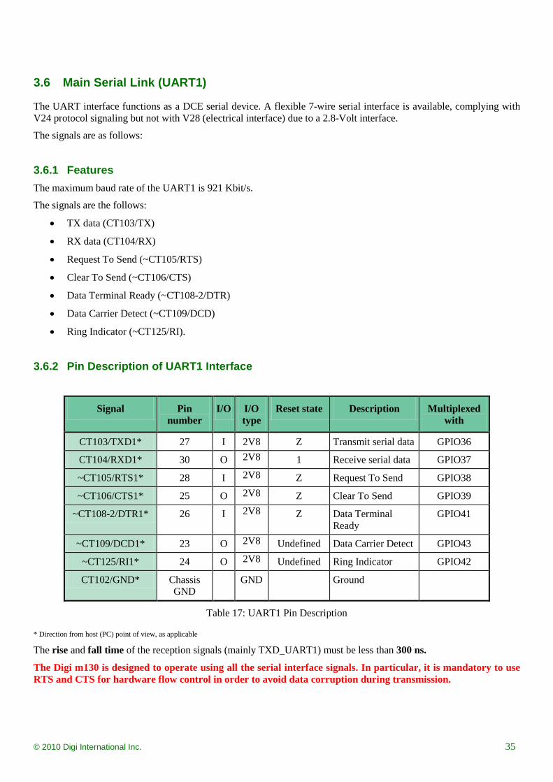
3.6.2 Pin Description of UART1 Interface
Signal Pin number
I/O I/O type
Reset state Description Multiplexed with
CT103/TXD1* 27 I 2V8 Z Transmit serial data GPIO36
CT104/RXD1* 30 O 2V8 1 Receive serial data GPIO37
~CT105/RTS1* 28 I 2V8 Z Request To Send GPIO38
~CT106/CTS1* 25 O 2V8 Z Clear To Send GPIO39
~CT108-2/DTR1* 26 I 2V8 Z Data Terminal Ready
GPIO41
~CT109/DCD1* 23 O 2V8 Undefined Data Carrier Detect GPIO43
~CT125/RI1* 24 O 2V8 Undefined Ring Indicator GPIO42
CT102/GND* Chassis GND
GND Ground
Table 17: UART1 Pin Description
* Direction from host (PC) point of view, as applicable
The rise and fall time of the reception signals (mainly TXD_UART1) must be less than 300 ns.
The Digi m130 is designed to operate using all the serial interface signals. In particular, it is mandatory to use RTS and CTS for hardware flow control in order to avoid data corruption during transmission.
Omni Product Technical Specification
© 2010 Digi International Inc. 36
Signal: CT103/TXD1*, CT104/RXD1*, ~CT105/RTS1*, ~CT106/CTS1*
Use-case with 5-wire serial interface
The signal ~CT108-2/DTR1* must be managed following the V24 protocol signalling if we want to use the slow idle mode
The other signals and their multiplexed are not available
For more information, please refer to the documents:
[1] ADL User Guide for OS v6.00 or later. Reference: WM_DEV_OAT_UGD_080
[2] DWLWin Download Application User. Guide. Reference: WM_DEV_TOO_UGD_010
[3] AT Command Interface Guide for Open AT® Firmware v7.0 or later. Reference: WM_DEV_OAT_UGD_059
CT103/TXD1*, CT104/RXD1*, ~CT105/RTS1*, ~CT106/CTS1*
Use-case with 4-wire serial interface
The signal ~CT108-2/DTR1* must be configured at the low level
The other signals and their multiplexed are not available
For more information, please refer to the documents:
[1] ADL User Guide for OS v6.00 or later. Reference: WM_DEV_OAT_UGD_080
[2] DWLWin Download Application User. Guide. Reference: WM_DEV_TOO_UGD_010
[3] AT Command Interface Guide for Open AT® Firmware v7.0 or later. Reference: WM_DEV_OAT_UGD_059
• This case is possible for connected external chip but not recommended (and forbidden for AT command or modem use)
Use-case with 2-wire serial interface
• The external chip must use flow control
• CT103/TXD1*, CT104/RXD1*
• The signal ~CT108-2/DTR1* must be configured at the low level
• The signals ~CT105/RTS1*, ~CT106/CTS1* are not used, please configure the AT command (AT+IFC=0,0
For further information, Please see documents:
[1] ADL User Guide for OS v6.00 or later. Reference: WM_DEV_OAT_UGD_080
[2] DWLWin Download Application User. Guide. Reference: WM_DEV_TOO_UGD_010
[3] AT Command Interface Guide for Open AT® Firmware v7.0 or later. Reference: WM_DEV_OAT_UGD_059
The signal ~CT105/RTS1* must be configured at the low level
• The other signals and their multiplexed are not available
For more information please refer to the documents:
[1] ADL User Guide for OS v6.00 or later. Reference: WM_DEV_OAT_UGD_080
[2] DWLWin Download Application User. Guide. Reference: WM_DEV_TOO_UGD_010
Omni Product Technical Specification
© 2010 Digi International Inc. 37
CustomerApplication
( DTE )
Digi m130( DCE )
~PWR_EN
CT103-TXD1 / GPIO36
CT104-RXD1 / GPIO37
~CT105-RTS1 / GPIO38
~CT106-CTS1 / GOPI39
12
5, 6, 21, 22
28
30
27
GND
Rx
RTS
CTS
GND
Tx
25
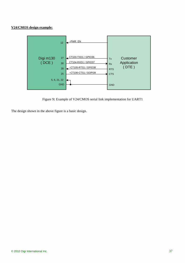
V24/CMOS design example:
Figure 9: Example of V24/CMOS serial link implementation for UART1
The design shown in the above figure is a basic design.
Omni Product Technical Specification
© 2010 Digi International Inc. 38
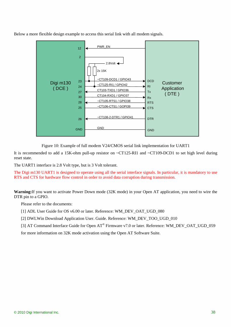
Below a more flexible design example to access this serial link with all modem signals.
Customer Application
( DTE )
Digi m130( DCE )
GND
PWR_EN
~CT109-DCD1 / GPIO43
~CT108-2-DTR1 / GPIO41
~CT125-RI1 / GPIO42
12
23
26
24
GND
DCD
DTR
RI
GND
CT103-TXD1 / GPIO36
CT104-RXD1 / GPIO37
~CT105-RTS1 / GPIO38
~CT106-CTS1 / GOPI3925
28
3027
RxRTS
CTS
Tx
2x 15K
2.8Volt
2
Figure 10: Example of full modem V24/CMOS serial link implementation for UART1
It is recommended to add a 15K-ohm pull-up resistor on ~CT125-RI1 and ~CT109-DCD1 to set high level during reset state.
The UART1 interface is 2.8 Volt type, but is 3 Volt tolerant.
The Digi m130 UART1 is designed to operate using all the serial interface signals. In particular, it is mandatory to use RTS and CTS for hardware flow control in order to avoid data corruption during transmission.
Warning:If you want to activate Power Down mode (32K mode) in your Open AT application, you need to wire the DTR pin to a GPIO.
Please refer to the documents:
[1] ADL User Guide for OS v6.00 or later. Reference: WM_DEV_OAT_UGD_080
[2] DWLWin Download Application User. Guide. Reference: WM_DEV_TOO_UGD_010
[3] AT Command Interface Guide for Open AT® Firmware v7.0 or later. Reference: WM_DEV_OAT_UGD_059
for more information on 32K mode activation using the Open AT Software Suite.

Omni Product Technical Specification
© 2010 Digi International Inc. 39
3.7 Auxiliary Serial Link (UART2)
3.7.1 Features The maximum baud rate of UART2 is 921 kbit/s.
For peripheral connectivity an auxiliary serial interface (UART2) is available on the system connector only on series without GPS functionality. On Digi m130 series with GPS functionality GPIO16 and GPIO17 are available.
The signals are the follows:
• TX data (CT103/TX) • RX data (CT104/RX) • Request To Send (~CT105/RTS) • Clear To Send (~CT106/CTS)
The Digi m130 is designed to operate using all the serial interface signals. In particular, it is mandatory to use RTS and CTS for hardware flow control in order to avoid data corruption during transmission.
This case is possible for connected external chip but not recommended (and forbidden for AT command or modem use)
Use-case with 2-wire serial interface
The external chip must be a flow control
CT103/TXD2*, CT104/RXD2*
The signals ~CT105/RTS2*, ~CT106/CTS2* are not used, please configure the AT command (AT+IFC=0,0.
Please refer to the documents:
[1] ADL User Guide for OS v6.00 or later. Reference: WM_DEV_OAT_UGD_080
[2] DWLWin Download Application User. Guide. Reference: WM_DEV_TOO_UGD_010
[3] AT Command Interface Guide for Open AT® Firmware v7.0 or later. Reference: WM_DEV_OAT_UGD_059.
The signal ~CT105/RTS2* must be configured at the low level
The other signal and their multiplexed are not available
Please refer to the document
[1] ADL User Guide for OS v6.00 or later. Reference: WM_DEV_OAT_UGD_080
[2] DWLWin Download Application User. Guide. Reference: WM_DEV_TOO_UGD_010
[3] AT Command Interface Guide for Open AT® Firmware v7.0 or later. Reference: WM_DEV_OAT_UGD_059
Signal Pin number
I/O I/O type Reset state
Description Multiplexed with
TXD2 37 I 1V8 Z Transmit serial data GPIO14
RXD2 39 O 1V8 Z Receive serial data GPIO15
CTS2 38 O 1V8 Z Clear To Send GPIO16
RTS2 40 I 1V8 Z Request To Send GPIO17
Table 18: UART2 Pin Description
Omni Product Technical Specification
© 2010 Digi International Inc. 40
See Chapter 3.4, “Electrical information for digital I/O” for Open drain, 2V8 and 1V8 voltage characteristics and Reset state definitions.
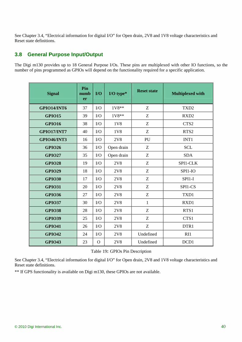
3.8 General Purpose Input/Output
The Digi m130 provides up to 18 General Purpose I/Os. These pins are multiplexed with other IO functions, so the number of pins programmed as GPIOs will depend on the functionality required for a specific application.
Signal Pin
number
I/O I/O type* Reset state Multiplexed with
GPIO14/INT6 37 I/O 1V8** Z TXD2
GPIO15 39 I/O 1V8** Z RXD2
GPIO16 38 I/O 1V8 Z CTS2
GPIO17/INT7 40 I/O 1V8 Z RTS2
GPIO46/INT3 16 I/O 2V8 PU INT1
GPIO26 36 I/O Open drain Z SCL
GPIO27 35 I/O Open drain Z SDA
GPIO28 19 I/O 2V8 Z SPI1-CLK
GPIO29 18 I/O 2V8 Z SPI1-IO
GPIO30 17 I/O 2V8 Z SPI1-I
GPIO31 20 I/O 2V8 Z SPI1-CS
GPIO36 27 I/O 2V8 Z TXD1
GPIO37 30 I/O 2V8 1 RXD1
GPIO38 28 I/O 2V8 Z RTS1
GPIO39 25 I/O 2V8 Z CTS1
GPIO41 26 I/O 2V8 Z DTR1
GPIO42 24 I/O 2V8 Undefined RI1
GPIO43 23 O 2V8 Undefined DCD1
Table 19: GPIOs Pin Description
See Chapter 3.4, “Electrical information for digital I/O” for Open drain, 2V8 and 1V8 voltage characteristics and Reset state definitions. ** If GPS functionality is available on Digi m130, these GPIOs are not available.

Omni Product Technical Specification
© 2010 Digi International Inc. 41
3.9 Analog to Digital Converters
3.9.1 Features Two Analog to Digital Converter inputs are provided by the Digi m130. The converters are 10-bit resolution, ranging from 0 to 2V.
Parameter Min Typ Max Unit
Resolution 10 bits
Sampling rate 216 S/s
Integral Accuracy 15 mV
Differential Accuracy 2.5 mV
Input signal range 0 2 V
Input impedance
ADC0 1M Ω
ADC1 1M Ω
Table 20: ADCs Electrical Characteristics
3.9.2 Pin Description
Table 21: ADCs Pin Description
Signal Pin number I/O I/O type Description
ADC0 13 I Analog A/D converter
ADC1 14 I Analog A/D converter
Omni Product Technical Specification
© 2010 Digi International Inc. 42
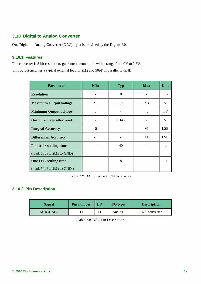
3.10 Digital to Analog Converter
One Digital to Analog Converter (DAC) input is provided by the Digi m130.
3.10.1 Features The converter is 8-bit resolution, guaranteed monotonic with a range from 0V to 2.3V.
This output assumes a typical external load of 2kΩ and 50pF in parallel to GND.
Parameter Min Typ Max Unit
Resolution - 8 - bits
Maximum Output voltage 2.1 2.2 2.3 V
Minimum Output voltage 0 - 40 mV
Output voltage after reset - 1.147 - V
Integral Accuracy -5 - +5 LSB
Differential Accuracy -1 - +1 LSB
Full scale settling time
(load: 50pF // 2kΩ to GND)
- 40 - µs
One LSB settling time
(load: 50pF // 2kΩ to GND )
- 8 - µs
Table 22: DAC Electrical Characteristics
3.10.2 Pin Description
Signal Pin number I/O I/O type Description
AUX-DAC0 11 O Analog D/A converter
Table 23: DAC Pin Description
Omni Product Technical Specification
© 2010 Digi International Inc. 43
3.11 Analog Audio Interface
The Digi m130 provides a single ended microphone input and single ended speaker output for GSM audio I/O. An echo cancellation feature allows hands free functionality in GSM voice mode.
3.11.1 Microphone Input
3.11.1.1 Features The MIC input includes the biasing for an electret microphone, thus allowing easy connection. The gain of the MIC input is internally adjusted and may be tuned using an AT command. AC coupling is already embedded in the Digi m130.
When you design the audio analog interface be sure to have a very good ground plane, a very good filtering as well as shielding in order to avoid any disturbance on the audio path.
Signal Pin number
I/O I/O type Description
MIC 10 I Analog Microphone input
Table 24: MIC2 Pin Description
3.11.1.1.1 Electrical Characteristics
Parameter Min. Typ Max. Unit
Internal Biasing
Voltage 2 2.1 2.2 V Output Current 0.5 1.5 mA
Impedance single-ended
Internal AC coupling 100 nF MIC to AGND 0.9 1.1 1.4 kΩ
Input voltage* Positive* 7.35 V Negative -0.9 V
Table 25: MIC2 Electrical Characteristics • *The input voltage depends on the input microphone gain set by AT command. • ** Because MIC2 is internally biased, a coupling capacitor must be used to connect an audio signal provided
by an active generator. Only a passive microphone may be directly connected to the MIC2 input.
Omni Product Technical Specification
© 2010 Digi International Inc. 44
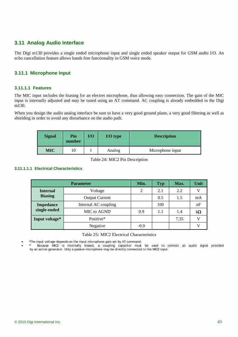
3.11.1.2 Application Example
10
AudioADC
Z2*= 1100 Ω typ
2.1V typ
100nF
Digi m130
MIC
C1MIC
L1
C2
Figure 11: Example of MIC input connection with LC filter *:Z2 is from 200Hz to 4kHz. For more characteristics refer to the chapter 3.14.1.1.2.
Internal input impedance value becomes 1100 ohms.
It is recommended to add L1 and C2 footprint to add a LC filter to try to eliminate the TDMA noise.
When not used, the filter can be removed by replacing L1 by a 0 Ohm resistor and by disconnecting C2, as the following schematic.
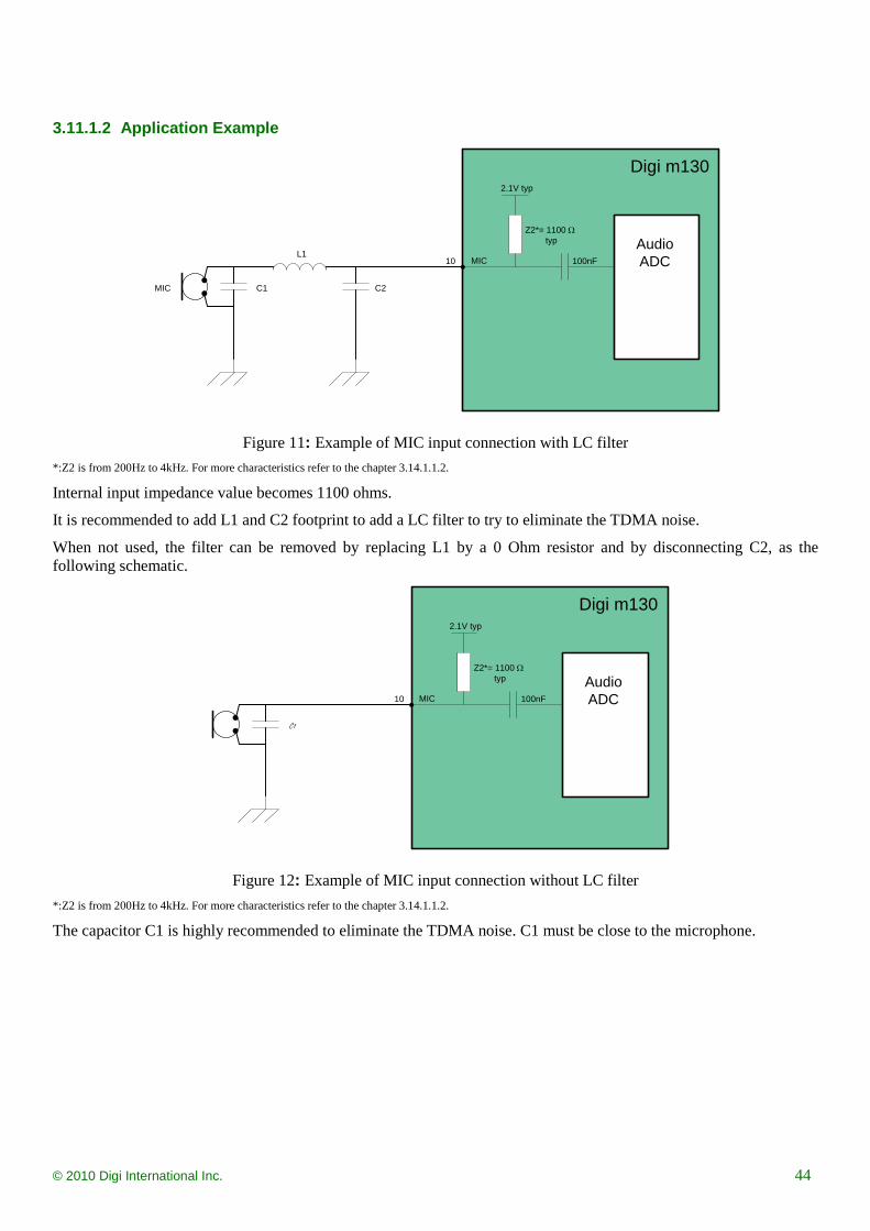
10
AudioADC
Z2*= 1100 Ω typ
2.1V typ
100nF
Digi m130
MIC
C1
Figure 12: Example of MIC input connection without LC filter *:Z2 is from 200Hz to 4kHz. For more characteristics refer to the chapter 3.14.1.1.2.
The capacitor C1 is highly recommended to eliminate the TDMA noise. C1 must be close to the microphone.
Omni Product Technical Specification
© 2010 Digi International Inc. 45
C1: 12pF to 33pF (depending of the design ,needs to be tuned )
Recommended components:
C2: Must be tuned depending of the design.
L1: Must be tuned depending of the design.
3.11.2 Speaker Output Characteristics
3.11.2.1 Features The connection is single-ended on SPK. Be sure to have a good ground plane, good filtering and adequate shielding in order to avoid any disturbance on the audio path.
Signal Pin number
I/O I/O type Description
SPK 7 O Analog Speaker Output
Table 26: SPK Pin Description
3.11.2.2 Electrical Characteristics
Parameters Min Typ Max Unit
Biasing voltage SPK 1.30 V
Output swing voltage
RL=8Ω: AT+VGR=6* - - 2 Vpp
RL=32Ω: AT+VGR=6* - - 2.5 Vpp
RL Load resistance 6 8 - Ω
IOUT Output current; peak value; RL=8Ω - - 90 mA
POUT RL=8Ω; AT+VGR=6*; - - 125 mW
RPD Output pull-down resistance at power-down 28 40 52 KΩ
VPD Output DC voltage at power-down - - 100 mV
Table 27: SPK Electrical Characteristics *The output voltage depends of the output speaker gain set by AT command.
Please refer to the documents:
[1] ADL User Guide for OS v6.00 or later. Reference: WM_DEV_OAT_UGD_080 [2] DWLWin Download Application User. Guide. Reference: WM_DEV_TOO_UGD_010 [3] AT Command Interface Guide for Open AT® Firmware v7.0 or later. Reference: WM_DEV_OAT_UGD_059
Omni Product Technical Specification
© 2010 Digi International Inc. 46
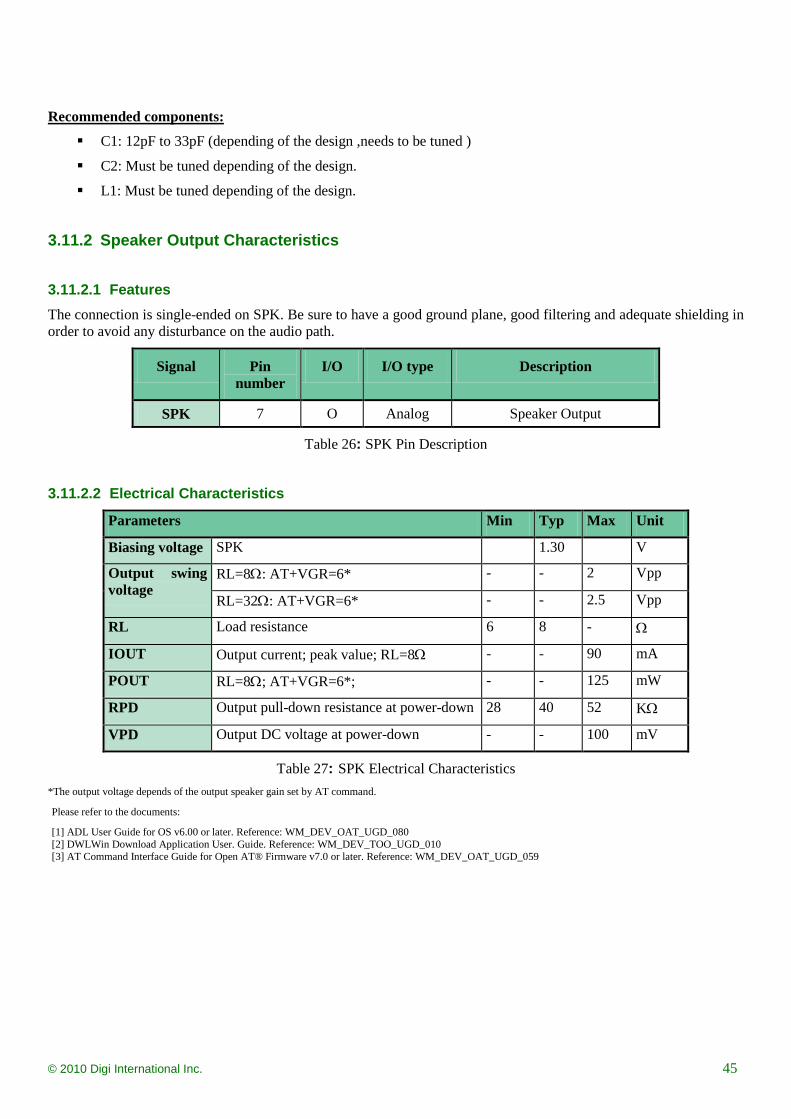
3.11.2.3 Application Example
SPK
C1 +
Z hp
Speaker
C3 33 pFto
100 pF
Figure 13: Example of Speaker connection
4.7 µF < C1 < 47 µF (depending on speaker characteristics and output power).
The connection between the Digi m130 pin and the speaker must be designed to keep the serial impedance lower than 1.5 Ω in single-ended mode.
3.11.3 Design Recommendation
3.11.3.1 General When speakers and microphones are exposed to the external environment, it is recommended to add ESD protection as closed as possible to the speaker or microphone, connected between the audio lines and a good ground.
You ensure to have a good ground plane, a good filtering as well as shielding, in order to avoid any disturbance on the audio path.
It is important to select an appropriate microphone, speaker and filtering components to avoid TDMA noise
3.11.3.2 Recommended Microphone Characteristics
The impedance of the microphone has to be around 2 kΩ.
Sensitivity from -40dB to –50 dB.
SNR > 50 dB.
Frequency response compatible with the GSM specifications.
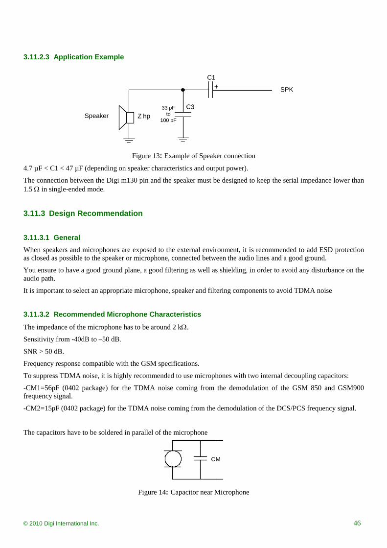
To suppress TDMA noise, it is highly recommended to use microphones with two internal decoupling capacitors:
-CM1=56pF (0402 package) for the TDMA noise coming from the demodulation of the GSM 850 and GSM900 frequency signal.
-CM2=15pF (0402 package) for the TDMA noise coming from the demodulation of the DCS/PCS frequency signal.
The capacitors have to be soldered in parallel of the microphone
CM
Figure 14: Capacitor near Microphone
Omni Product Technical Specification
© 2010 Digi International Inc. 47
3.11.3.3 Recommended Speaker Characteristics Type of speakers: Electro-magnetic /10mW Impedance: 8Ω for hands-free (SPK2) Sensitivity: 110dB SPL min Receiver frequency response compatible with the GSM specifications.
3.11.3.4 Recommended Filtering Components When designing a GSM application, it is important to select the right audio filtering components.
The strongest noise, called TDMA, is mainly due to the demodulation of the GSM850/GSM900/DCS1800 and PCS1900 signal: A burst being produced every 4.615ms; the frequency of the TDMA signal is equal to 216.7Hz plus harmonics.
The TDMA noise can be suppress by filtering the RF signal using the right decoupling components.
The types of filtering components are:
• -RF decoupling inductors
• -RF decoupling capacitors
Murata offers an application enabling you to calculate, view and print graphs of the impedance and S parameter data for chip capacitors or chip inductors. S parameter data in Touchstone format can also be copied:
Based on the use of different Murata components, the value, the package and the current rating can have different decoupling effects.
http://www.murata.com/products/design_support/mcsil/index.html
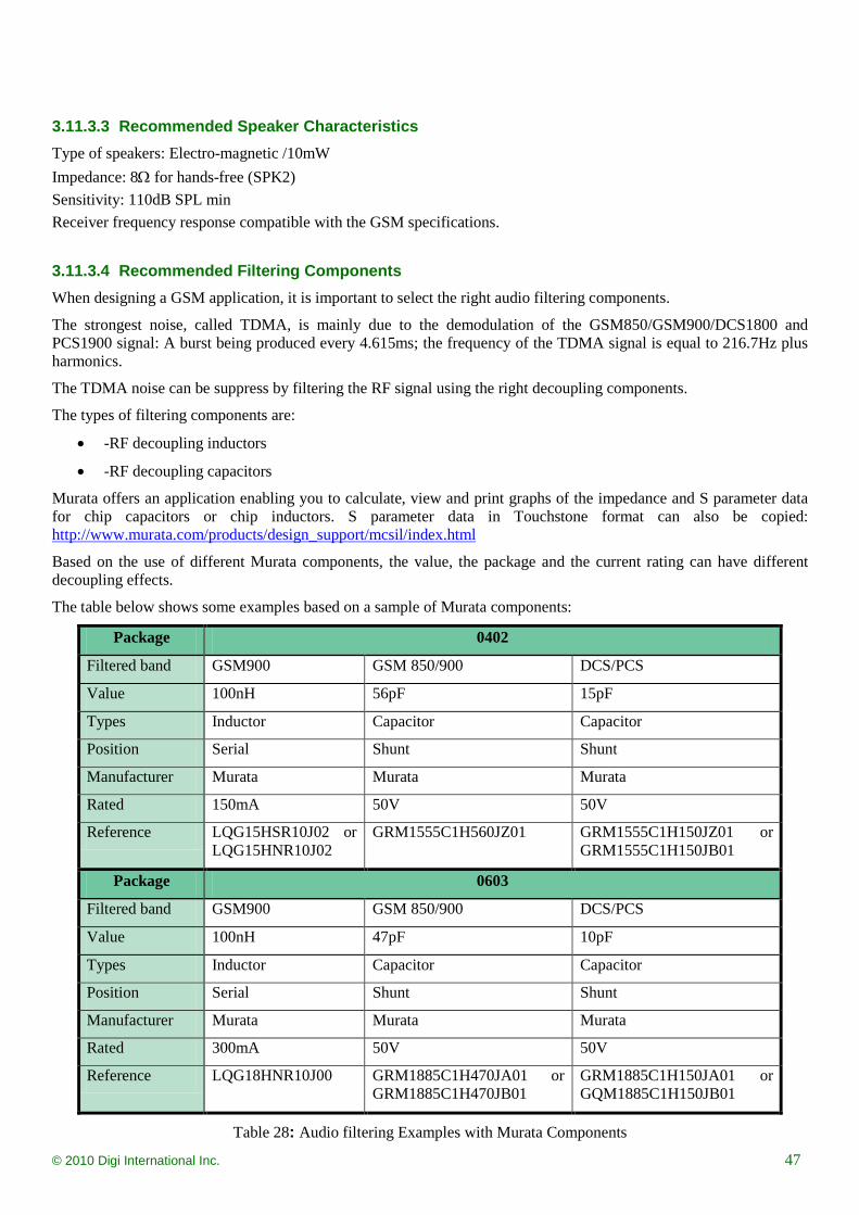
The table below shows some examples based on a sample of Murata components:
Package 0402
Filtered band GSM900 GSM 850/900 DCS/PCS
Value 100nH 56pF 15pF
Types Inductor Capacitor Capacitor
Position Serial Shunt Shunt
Manufacturer Murata Murata Murata
Rated 150mA 50V 50V
Reference LQG15HSR10J02 or LQG15HNR10J02
GRM1555C1H560JZ01 GRM1555C1H150JZ01 or GRM1555C1H150JB01
Package 0603
Filtered band GSM900 GSM 850/900 DCS/PCS
Value 100nH 47pF 10pF
Types Inductor Capacitor Capacitor
Position Serial Shunt Shunt
Manufacturer Murata Murata Murata
Rated 300mA 50V 50V
Reference LQG18HNR10J00 GRM1885C1H470JA01 or GRM1885C1H470JB01
GRM1885C1H150JA01 or GQM1885C1H150JB01
Table 28: Audio filtering Examples with Murata Components
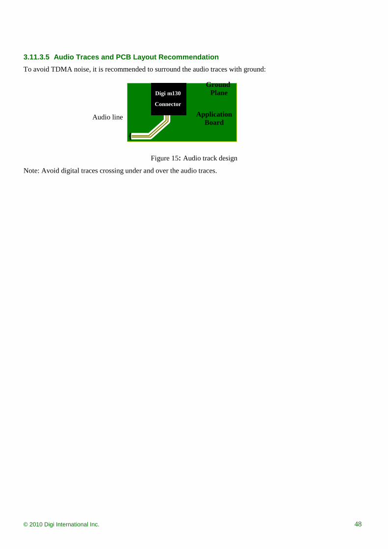
Omni Product Technical Specification
© 2010 Digi International Inc. 48
3.11.3.5 Audio Traces and PCB Layout Recommendation To avoid TDMA noise, it is recommended to surround the audio traces with ground:
Figure 15: Audio track design
Note: Avoid digital traces crossing under and over the audio traces.
Audio line Application Board
Ground Plane Digi m130
Connector
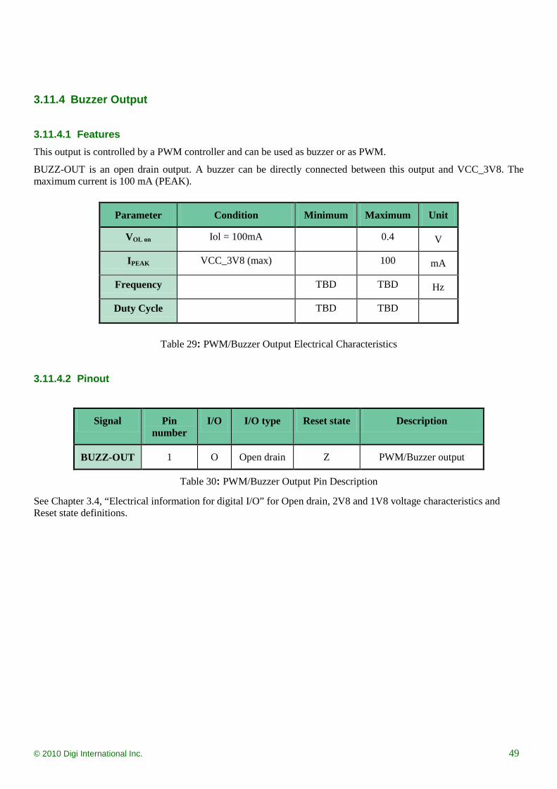
Omni Product Technical Specification
© 2010 Digi International Inc. 49
3.11.4 Buzzer Output
3.11.4.1 Features This output is controlled by a PWM controller and can be used as buzzer or as PWM.
BUZZ-OUT is an open drain output. A buzzer can be directly connected between this output and VCC_3V8. The maximum current is 100 mA (PEAK).
Table 29: PWM/Buzzer Output Electrical Characteristics
3.11.4.2 Pinout
Signal Pin number
I/O I/O type Reset state Description
BUZZ-OUT 1 O Open drain Z PWM/Buzzer output
Table 30: PWM/Buzzer Output Pin Description
See Chapter 3.4, “Electrical information for digital I/O” for Open drain, 2V8 and 1V8 voltage characteristics and Reset state definitions.
Parameter Condition Minimum Maximum Unit
VOL on Iol = 100mA 0.4 V
IPEAK VCC_3V8 (max) 100 mA
Frequency TBD TBD Hz
Duty Cycle TBD TBD
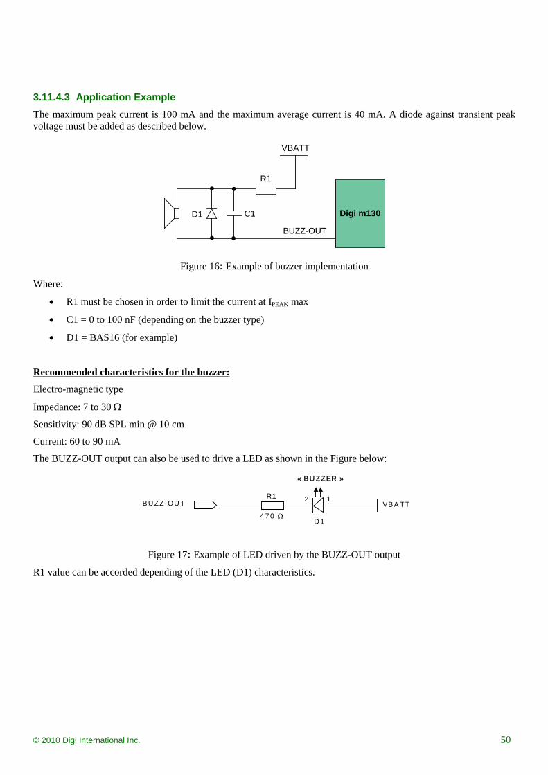
Omni Product Technical Specification
© 2010 Digi International Inc. 50
3.11.4.3 Application Example The maximum peak current is 100 mA and the maximum average current is 40 mA. A diode against transient peak voltage must be added as described below.
BUZZ-OUT
C1 D1
VBATT R1
Digi m130
Figure 16: Example of buzzer implementation
Where:
• R1 must be chosen in order to limit the current at IPEAK max
• C1 = 0 to 100 nF (depending on the buzzer type)
• D1 = BAS16 (for example)
Electro-magnetic type
Recommended characteristics for the buzzer:
Impedance: 7 to 30 Ω
Sensitivity: 90 dB SPL min @ 10 cm
Current: 60 to 90 mA
The BUZZ-OUT output can also be used to drive a LED as shown in the Figure below:
BU ZZ-OU T VBA TT
« B U ZZER »
D 1
12R1
4 7 0 Ω
Figure 17: Example of LED driven by the BUZZ-OUT output
R1 value can be accorded depending of the LED (D1) characteristics.
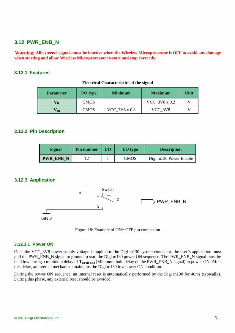
Omni Product Technical Specification
© 2010 Digi International Inc. 51
3.12 PWR_ENB_N
Warning:
3.12.1 Features
All external signals must be inactive when the Wireless Microprocessor is OFF to avoid any damage when starting and allow Wireless Microprocessor to start and stop correctly.
Electrical Characteristics of the signal
Parameter I/O type Minimum Maximum Unit
VIL CMOS VCC_3V8 x 0.2 V
VIH CMOS VCC_3V8 x 0.8 VCC_3V8 V
3.12.2 Pin Description
Signal Pin number I/O I/O type Description
PWR_ENB_N 12 I CMOS Digi m130 Power Enable
3.12.3 Application
12
3
Switch
PWR_ENB_N
GND
Figure 18: Example of ON/~OFF pin connection
3.12.3.1 Power ON Once the VCC_3V8 power supply voltage is applied to the Digi m130 system connector, the user’s application must pull the PWR_ENB_N signal to ground to start the Digi m130 power ON sequence. The PWR_ENB_N signal must be held low during a minimum delay of Ton/off-hold (Minimum hold delay on the PWR_ENB_N signal) to power-ON. After this delay, an internal mechanism maintains the Digi m130 in a power ON condition.
During the power ON sequence, an internal reset is automatically performed by the Digi m130 for 40ms (typically). During this phase, any external reset should be avoided.
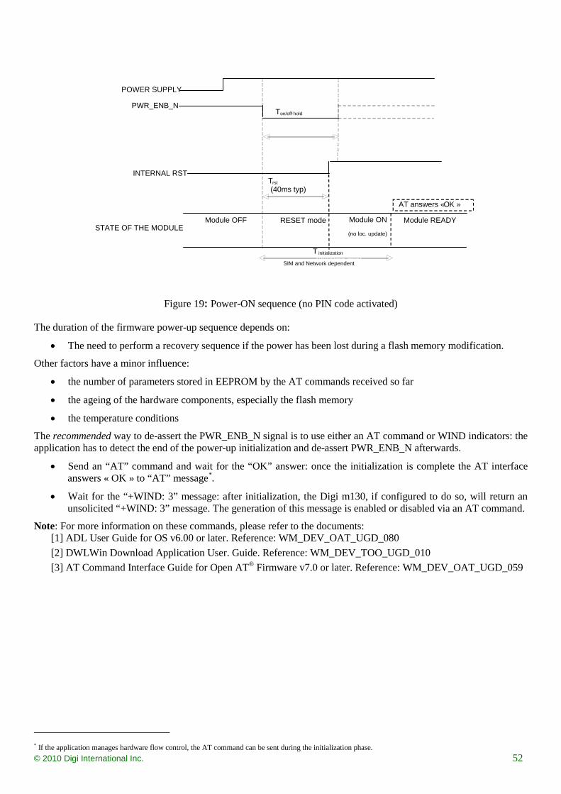
Omni Product Technical Specification
© 2010 Digi International Inc. 52
POWER SUPPLY
PWR_ENB_N
STATE OF THE MODULE Module OFF I BB+RF < 22µA
AT answers « OK »
Module READY
Ton/off-hold
(2000ms min)
SIM and Network dependent
RESET mode IBB+RF =20 to 40mA
INTERNAL RST Trst
(40ms typ)
Module ON IBB+RF <120mA (no loc. update)
T initialization (2000ms min)
Figure 19: Power-ON sequence (no PIN code activated)
The duration of the firmware power-up sequence depends on:
• The need to perform a recovery sequence if the power has been lost during a flash memory modification.
Other factors have a minor influence:
• the number of parameters stored in EEPROM by the AT commands received so far
• the ageing of the hardware components, especially the flash memory
• the temperature conditions
The recommended way to de-assert the PWR_ENB_N signal is to use either an AT command or WIND indicators: the application has to detect the end of the power-up initialization and de-assert PWR_ENB_N afterwards.
• Send an “AT” command and wait for the “OK” answer: once the initialization is complete the AT interface answers « OK » to “AT” message*
• Wait for the “+WIND: 3” message: after initialization, the Digi m130, if configured to do so, will return an unsolicited “+WIND: 3” message. The generation of this message is enabled or disabled via an AT command.
.
Note: For more information on these commands, please refer to the documents: [1] ADL User Guide for OS v6.00 or later. Reference: WM_DEV_OAT_UGD_080 [2] DWLWin Download Application User. Guide. Reference: WM_DEV_TOO_UGD_010 [3] AT Command Interface Guide for Open AT® Firmware v7.0 or later. Reference: WM_DEV_OAT_UGD_059
* If the application manages hardware flow control, the AT command can be sent during the initialization phase.
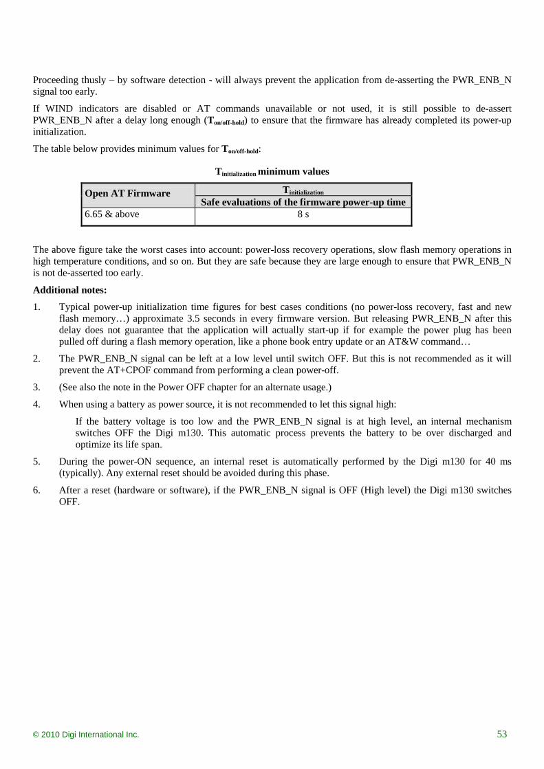
Omni Product Technical Specification
© 2010 Digi International Inc. 53
Proceeding thusly – by software detection - will always prevent the application from de-asserting the PWR_ENB_N signal too early.
If WIND indicators are disabled or AT commands unavailable or not used, it is still possible to de-assert PWR_ENB_N after a delay long enough (Ton/off-hold) to ensure that the firmware has already completed its power-up initialization.
The table below provides minimum values for Ton/off-hold:
Tinitialization minimum values
Open AT Firmware Tinitialization Safe evaluations of the firmware power-up time
6.65 & above 8 s
The above figure take the worst cases into account: power-loss recovery operations, slow flash memory operations in high temperature conditions, and so on. But they are safe because they are large enough to ensure that PWR_ENB_N is not de-asserted too early.
Additional notes:
1. Typical power-up initialization time figures for best cases conditions (no power-loss recovery, fast and new flash memory…) approximate 3.5 seconds in every firmware version. But releasing PWR_ENB_N after this delay does not guarantee that the application will actually start-up if for example the power plug has been pulled off during a flash memory operation, like a phone book entry update or an AT&W command…
2. The PWR_ENB_N signal can be left at a low level until switch OFF. But this is not recommended as it will prevent the AT+CPOF command from performing a clean power-off.
3. (See also the note in the Power OFF chapter for an alternate usage.)
4. When using a battery as power source, it is not recommended to let this signal high:
If the battery voltage is too low and the PWR_ENB_N signal is at high level, an internal mechanism switches OFF the Digi m130. This automatic process prevents the battery to be over discharged and optimize its life span.
5. During the power-ON sequence, an internal reset is automatically performed by the Digi m130 for 40 ms (typically). Any external reset should be avoided during this phase.
6. After a reset (hardware or software), if the PWR_ENB_N signal is OFF (High level) the Digi m130 switches OFF.
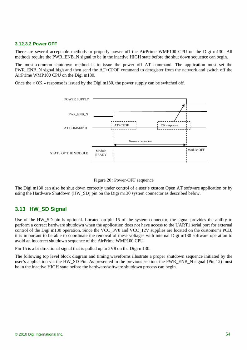
Omni Product Technical Specification
© 2010 Digi International Inc. 54
3.12.3.2 Power OFF There are several acceptable methods to properly power off the AirPrime WMP100 CPU on the Digi m130. All methods require the PWR_ENB_N signal to be in the inactive HIGH state before the shut down sequence can begin.
The most common shutdown method is to issue the power off AT command. The application must set the PWR_ENB_N signal high and then send the AT+CPOF command to deregister from the network and switch off the AirPrime WMP100 CPU on the Digi m130.
Once the « OK » response is issued by the Digi m130, the power supply can be switched off.
PWR_ENB_N
POWER SUPPLY
AT COMMAND
STATE OF THE MODULE
AT+CPOF
Module READY
Module OFF IBB+RF<22µA
Network dependent
OK response
IBB+RF = overall current consumption (Base Band + RF part)
Figure 20: Power-OFF sequence
The Digi m130 can also be shut down correctly under control of a user’s custom Open AT software application or by using the Hardware Shutdown (HW_SD) pin on the Digi m130 system connector as described below.
3.13 HW_SD Signal
Use of the HW_SD pin is optional. Located on pin 15 of the system connector, the signal provides the ability to perform a correct hardware shutdown when the application does not have access to the UART1 serial port for external control of the Digi m130 operation. Since the VCC_3V8 and VCC_12V supplies are located on the customer’s PCB, it is important to be able to coordinate the removal of these voltages with internal Digi m130 software operation to avoid an incorrect shutdown sequence of the AirPrime WMP100 CPU.
Pin 15 is a bi-directional signal that is pulled up to 2V8 on the Digi m130.
The following top level block diagram and timing waveforms illustrate a proper shutdown sequence initiated by the user’s application via the HW_SD Pin. As presented in the previous section, the PWR_ENB_N signal (Pin 12) must be in the inactive HIGH state before the hardware/software shutdown process can begin.
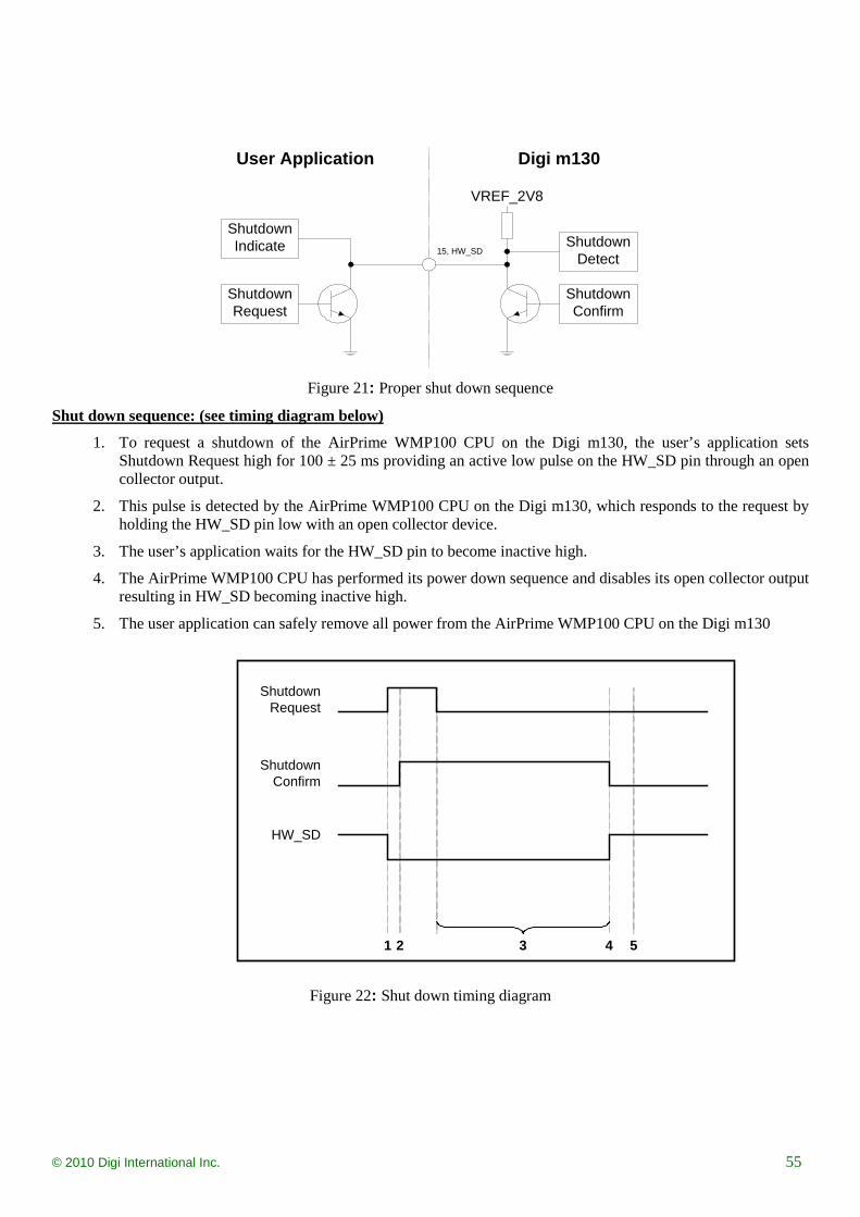
Omni Product Technical Specification
© 2010 Digi International Inc. 55
Figure 21: Proper shut down sequence
1. To request a shutdown of the AirPrime WMP100 CPU on the Digi m130, the user’s application sets Shutdown Request high for 100 ± 25 ms providing an active low pulse on the HW_SD pin through an open collector output.
Shut down sequence: (see timing diagram below)
2. This pulse is detected by the AirPrime WMP100 CPU on the Digi m130, which responds to the request by holding the HW_SD pin low with an open collector device.
3. The user’s application waits for the HW_SD pin to become inactive high.
4. The AirPrime WMP100 CPU has performed its power down sequence and disables its open collector output resulting in HW_SD becoming inactive high.
5. The user application can safely remove all power from the AirPrime WMP100 CPU on the Digi m130
Figure 22: Shut down timing diagram
Shutdown Indicate
Shutdown Request
Shutdown Confirm
Shutdown Detect
VREF_2V8
15, HW_SD
User Application Digi m130
HW_SD
ShutdownRequest
ShutdownConfirm
1 42 3 5
Omni Product Technical Specification
© 2010 Digi International Inc. 56
3.14 External Interrupt
The Digi m130 provides one external interrupt input. This interrupt (INT3) is configured and monitored by the user’s embedded Open AT software application. The interrupt input can be activated on:
• High to low edge
• Low to high edge
• Low to high and high to low edge
• Low level
• High level
Signal Pin number
I/O I/O type
Reset state
Description Multiplexed with
EXT_INT 16 I 2V8 PU External Interrupt (INT3) GPIO46
Table 31: External Interrupt Pin description
See Chapter 3.4, “Electrical information for digital I/O” for Open drain, 2V8 and 1V8 voltage characteristics and Reset state definitions.
Parameter Minimum Maximum Unit
EXT_INT (INT3) VIL 0.84 V
VIH 1.96 V
Table 32: External Interrupt Electrical Characteristics
3.15 BOOT Signal
A specific control signal BOOT is available to download Digi m130 firmware during the manufacturing process and for major software upgrades in the field if the standard XMODEM download, controlled with AT commands, is not applicable.
PC software, provided by Sierra Wireless, is needed to perform this download, specifically for the first download of the Flash memory.
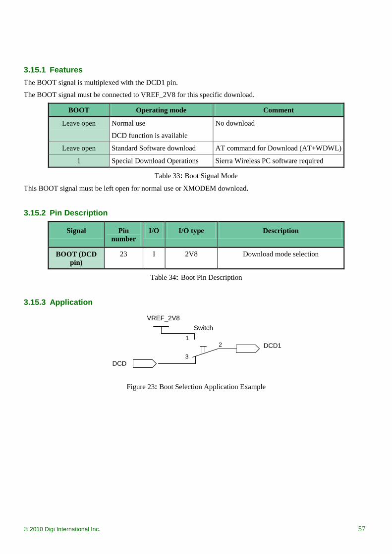
Omni Product Technical Specification
© 2010 Digi International Inc. 57
3.15.1 Features The BOOT signal is multiplexed with the DCD1 pin.
The BOOT signal must be connected to VREF_2V8 for this specific download.
BOOT Operating mode Comment
Leave open Normal use
DCD function is available
No download
Leave open Standard Software download AT command for Download (AT+WDWL)
1 Special Download Operations Sierra Wireless PC software required
Table 33: Boot Signal Mode
This BOOT signal must be left open for normal use or XMODEM download.
3.15.2 Pin Description
Signal Pin number
I/O I/O type Description
BOOT (DCD pin)
23 I 2V8 Download mode selection
Table 34: Boot Pin Description
3.15.3 Application
12
3
SwitchVREF_2V8
DCD
DCD1
Figure 23: Boot Selection Application Example
Omni Product Technical Specification
© 2010 Digi International Inc. 58
3.16 VREF_2V8 Output
This output can only be used to connect pull-up resistor. VCC_2V8 must be used as a reference supply. The voltage supply is available when the Digi m130 is on.
Signal Pin number I/O I/O type Description
VREF_2V8 2 O Supply Digital supply
Table 35: VREF_2V8 Pin Description
Parameter Minimum Typ Maximum Unit
VCC_2V8 Output voltage 2.74 2.8 2.86 V
Output Current 15 mA
Table 36: VREF_2V8 Electrical Characteristics
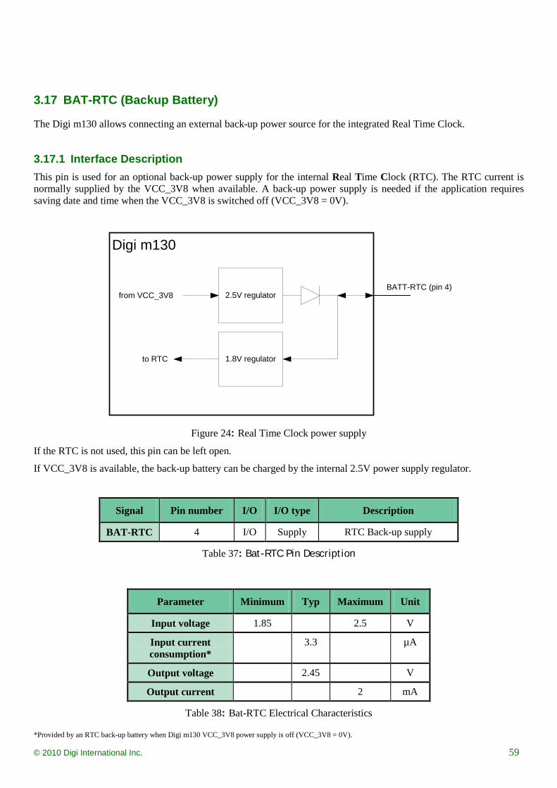
Omni Product Technical Specification
© 2010 Digi International Inc. 59
3.17 BAT-RTC (Backup Battery)
The Digi m130 allows connecting an external back-up power source for the integrated Real Time Clock.
3.17.1 Interface Description This pin is used for an optional back-up power supply for the internal Real Time Clock (RTC). The RTC current is normally supplied by the VCC_3V8 when available. A back-up power supply is needed if the application requires saving date and time when the VCC_3V8 is switched off (VCC_3V8 = 0V).
2.5V regulator
1.8V regulator
from VCC_3V8
to RTC
Digi m130
BATT-RTC (pin 4)
Figure 24: Real Time Clock power supply
If the RTC is not used, this pin can be left open.
If VCC_3V8 is available, the back-up battery can be charged by the internal 2.5V power supply regulator.
Signal Pin number I/O I/O type Description
BAT-RTC 4 I/O Supply RTC Back-up supply
Table 37: Bat-RTC Pin Description
Parameter Minimum Typ Maximum Unit
Input voltage 1.85 2.5 V
Input current consumption*
3.3 µA
Output voltage 2.45 V
Output current 2 mA
Table 38: Bat-RTC Electrical Characteristics
*Provided by an RTC back-up battery when Digi m130 VCC_3V8 power supply is off (VCC_3V8 = 0V).
Omni Product Technical Specification
© 2010 Digi International Inc. 60
3.18 FLASH-LED Signal
FLASH LED is an open drain output. An LED and a current limiting resistor can be directly connected between this output and the VCC_3V8 supply.
When the Digi m130 CPU is ON, this output is used to indicate network status.
GSM status
VCC_3V8 status FLASH-LED status Digi m130 GSM status
ON VCC_3V8 = 3.8V
Permanent Digi m130 switched ON, not registered on the network
Slow flash
LED ON for 200 ms, OFF for 2 s
Digi m130 switched ON, registered on the network
Quick flash
LED ON for 200 ms, OFF for 600 ms
Digi m130 switched ON, registered on the network, communication in progress
Very quick flash
LED ON for 100ms, OFF for 200ms
Digi m130 switched on, software downloaded is either corrupted or non-compatible ("BAD SOFTWARE")
Table 39: Flash-LED Status
Signal Pin number
I/O I/O type Reset state Description
FLASH-LED
3 O Open Drain Output
1 and Undefined
LED driving
Table 40: Flash-LED Pin Description
See Chapter 3.4, “Electrical information for digital I/O” for Open drain, 2V8 and 1V8 voltage characteristics and Reset state definitions.
FLASH-LED state is undefined during the software initialization time. During software initialization time, for 2 seconds max after POWER_EN is pulled active low, the FLASH-LED signal is toggling and does not provide Digi m130 GSM status. After the 2s period, the FLASH-LED provides the true status of the Digi m130 GSM connection.
Parameter Condition Minimum Typ Maximum Unit
VOL 0.4 V
IOUT 8 mA
Table 41: Flash-LED Electrical Characteristics
Omni Product Technical Specification
© 2010 Digi International Inc. 61
3.19 RF Interface
The RF impedance for GSM, Orbcomm and GPS* antenna outputs is 50 Ohms nominal and the DC impedance is 0 Ohm.
The GPS* interface provides 3V biasing for active antennas.
3.19.1 RF Performance
3.19.1.1 GSM Performance
3.19.1.1.1 GSM RF Performance GSM mode RF performance is compliant with the ETSI GSM 05.05 recommendation.
The GSM Receiver parameters are:
• GSM850 Reference Sensitivity = -108 dBm Static & TUHigh
• E-GSM900 Reference Sensitivity = -108 dBm Static & TUHigh
• DCS1800 Reference Sensitivity = -107 dBm Static & TUHigh
• PCS1900 Reference Sensitivity = -107 dBm Static & TUHigh
• Selectivity @ 200 kHz: > +9 dBc
• Selectivity @ 400 kHz: > +41 dBc
• Linear dynamic range: 63 dB
• Co-channel rejection: >= 9 dBc
3.19.1.1.2 GSM Transmitter Parameters • Maximum output power (EGSM & GSM850): 33 dBm +/- 2 dB at ambient temperature
• Maximum output power (GSM1800 & PCS1900): 30 dBm +/- 2 dB at ambient temperature
• Minimum output power (EGSM & GSM850): 5 dBm +/- 5 dB at ambient temperature
• Minimum output power (GSM1800 & PCS1900): 0 dBm +/- 5 dB at ambient temperature
Omni Product Technical Specification
© 2010 Digi International Inc. 62
3.19.1.1.3 GSM Antenna Specifications The antenna must meet the following requirements:
The optimum operating frequency depends on the application. A dual band or quad band antenna shall operate in these frequency bands and have the following characteristics:
Characteristic Digi m130 GSM Mode of Operation
E-GSM 900 DCS 1800 GSM 850 PCS 1900
TX Frequency 880 to 915 MHz
1710 to 1785 MHz
824 to 849 MHz
1850 to 1910 MHz
RX Frequency 925 to 960 MHz
1805 to 1880 MHz
869 to 894 MHz
1930 to 1990 MHz
Impedance Nom. 50 Ohms
DC Ground Yes (zero ohms)
VSWR Rx max 1.5:1
Tx max 1.5:1 Typical radiated gain 0dBi in one direction at least
Table 42: GSM Antenna Specifications
3.19.1.2 Orbcomm Performance
3.19.1.2.1 Orbcomm RF Performance • Receiver frequency band: 137.0 to 138.0 MHz
• Receiver Sensitivity: - 118 dbm minimum at ambient
3.19.1.2.2 Orbcomm Transmitter Parameters • Transmitter frequency band: 148.0 to 150.05 MHz
• Maximum Output Power: +37dbm at ambient
Omni Product Technical Specification
© 2010 Digi International Inc. 63
3.19.1.2.3 Orbcomm Antenna Specifications
Characteristic Digi m130
Orbcomm Mode of Operation
TX Frequency 148.00 to 150.05 MHz
RX Frequency 137.00 to 138.00 MHz
Impedance Nom. 50 Ohms
DC Ground Yes (zero ohms)
VSWR Rx max 1.5:1
Tx max 1.5:1
Typical radiated gain +3dBi Omnidirectional
Note: We recommend using a covered radiating element antenna with this setup.
3.19.1.3 GPS Functionality The Digi m130 is available with an optional GPS receiver. The GPS is implemented with an e-Ride Opus III ® Chipset solution. This part is controlled by the Digi m130’s ARM9 CPU.
For a list of available commands refer to AT command list.
3.19.1.3.1 GPS Features • Supports GPS L-band C/A code channels and 2 additional dedicated WAAS channels for enhanced accuracy • High indoor sensitivity of -161dBm achieved utilizing 44,000 effective correlators (both in acquisition &
tracking mode) • Fast TTFF of typically < 1s when in hot and 34s in cold start conditions • Accuracy of 2.5m outdoors (CEP 50%) and 10m indoors • User interface via a serial port, 1Hz update rate
3.19.1.3.2 GPS Performance
Parameter Conditions Min Typ Max Unit
Hot Start @-135 dBm 1 s
Hot Start @-155 dBm All SV’s same level 13 s
Warm Start @-135 dBm 33 s
Warm Start @-145 dBm All SV’s same level 67 s
Cold Start @-135 dBm 34 s
Cold Start @-145 dBm All SV’s same level 83 s
Acquisition sensitivity, (hot start) -161 dBm
Acquisition sensitivity, (warm start) -146.5 dBm
Tracking sensitivity -161 dBm
Position accuracy, outdoors Open sky, CEP 50% 2.5 m
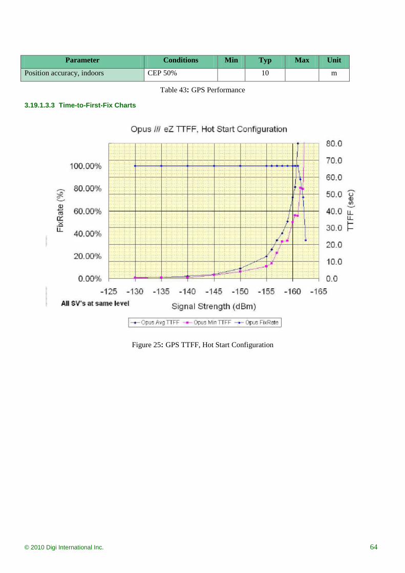
Omni Product Technical Specification
© 2010 Digi International Inc. 64
Parameter Conditions Min Typ Max Unit
Position accuracy, indoors CEP 50% 10 m
Table 43: GPS Performance
3.19.1.3.3 Time-to-First-Fix Charts
Figure 25: GPS TTFF, Hot Start Configuration
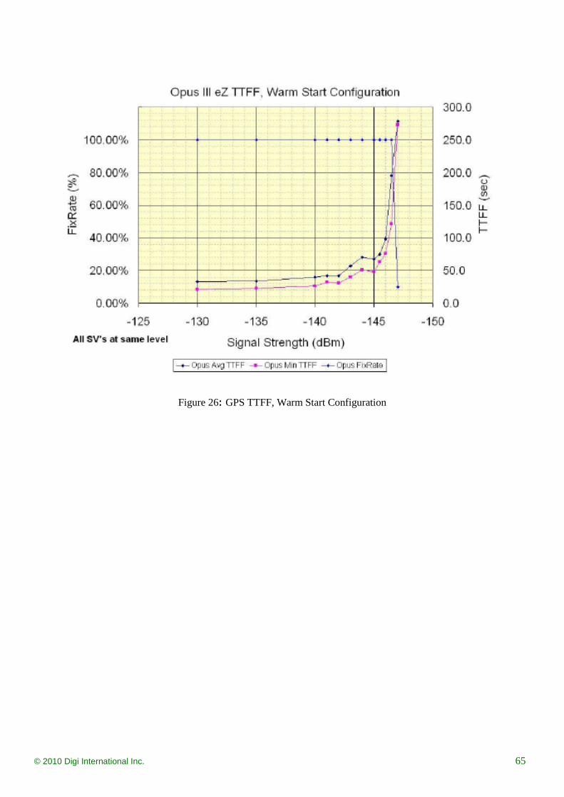
Omni Product Technical Specification
© 2010 Digi International Inc. 65
Figure 26: GPS TTFF, Warm Start Configuration
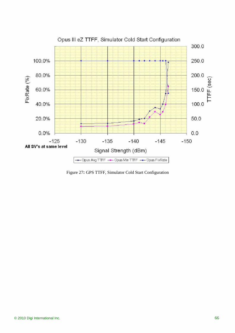
Omni Product Technical Specification
© 2010 Digi International Inc. 66
Figure 27: GPS TTFF, Simulator Cold Start Configuration
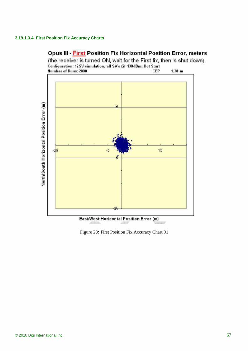
Omni Product Technical Specification
© 2010 Digi International Inc. 67
3.19.1.3.4 First Position Fix Accuracy Charts
Figure 28: First Position Fix Accuracy Chart 01
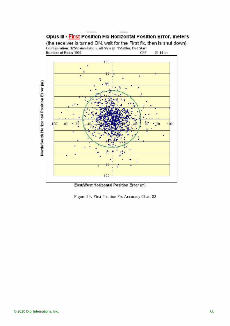
Omni Product Technical Specification
© 2010 Digi International Inc. 68
Figure 29: First Position Fix Accuracy Chart 02
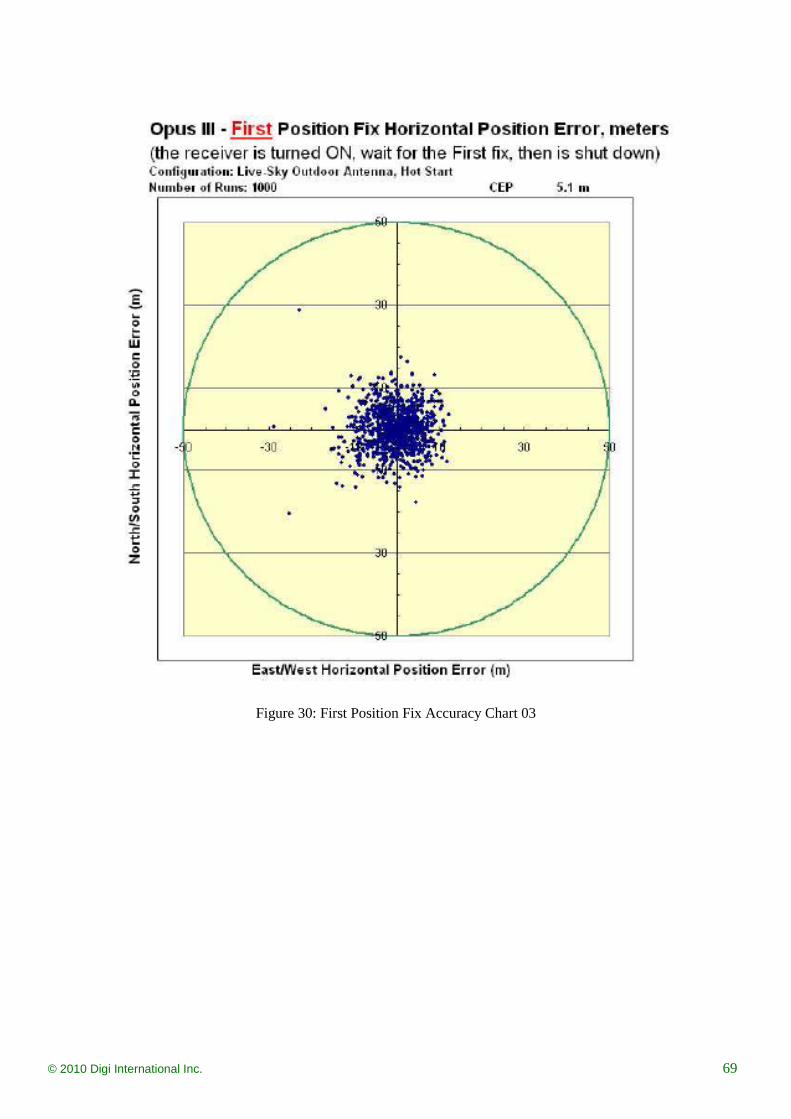
Omni Product Technical Specification
© 2010 Digi International Inc. 69
Figure 30: First Position Fix Accuracy Chart 03
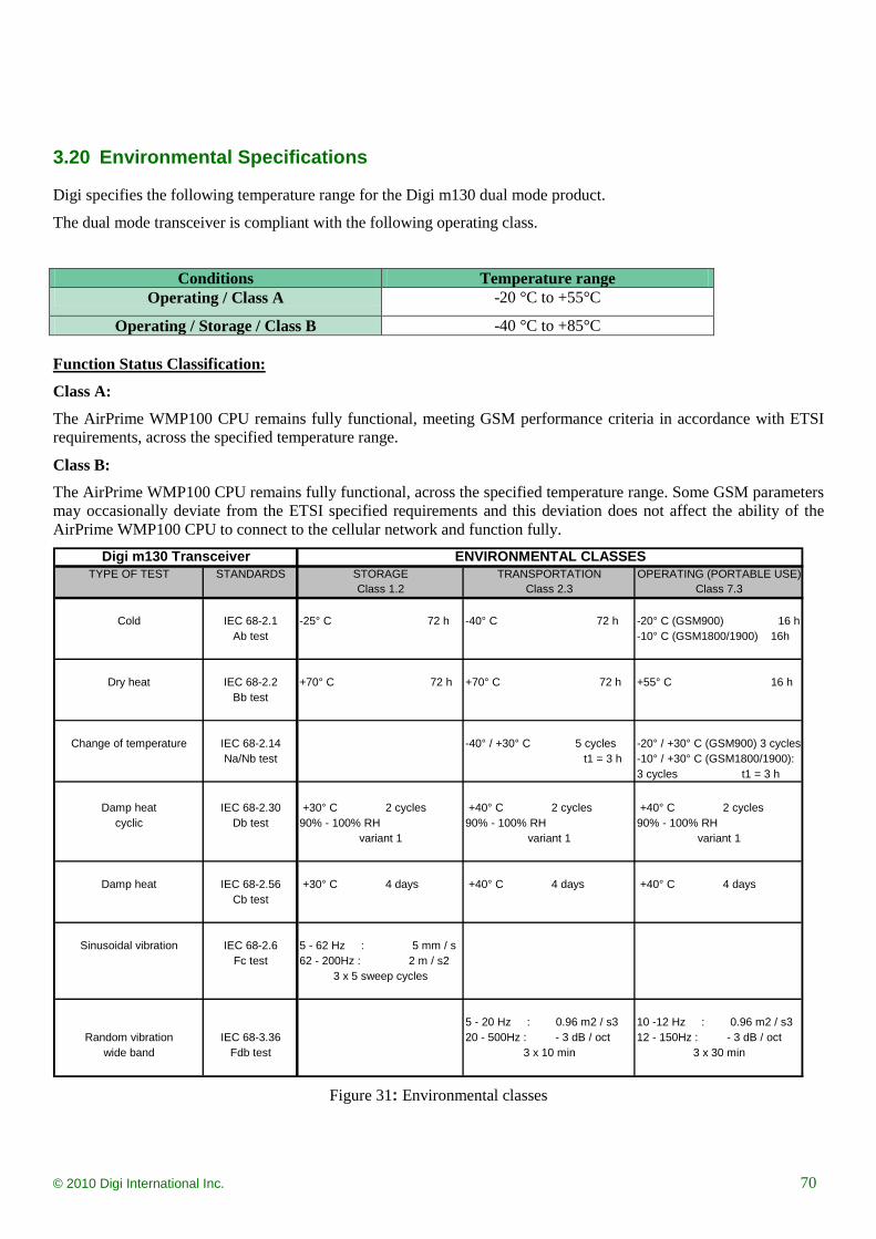
Omni Product Technical Specification
© 2010 Digi International Inc. 70
3.20 Environmental Specifications
Digi specifies the following temperature range for the Digi m130 dual mode product.
The dual mode transceiver is compliant with the following operating class.
Conditions Temperature range Operating / Class A -20 °C to +55°C
Operating / Storage / Class B -40 °C to +85°C
Class A:
Function Status Classification:
The AirPrime WMP100 CPU remains fully functional, meeting GSM performance criteria in accordance with ETSI requirements, across the specified temperature range.
Class B:
The AirPrime WMP100 CPU remains fully functional, across the specified temperature range. Some GSM parameters may occasionally deviate from the ETSI specified requirements and this deviation does not affect the ability of the AirPrime WMP100 CPU to connect to the cellular network and function fully.
Digi m130 Transceiver ENVIRONMENTAL CLASSESTYPE OF TEST STANDARDS STORAGE TRANSPORTATION OPERATING (PORTABLE USE)
Class 1.2 Class 2.3 Class 7.3
Cold IEC 68-2.1 -25° C 72 h -40° C 72 h -20° C (GSM900) 16 hAb test -10° C (GSM1800/1900) 16h
Dry heat IEC 68-2.2 +70° C 72 h +70° C 72 h +55° C 16 hBb test
Change of temperature IEC 68-2.14 -40° / +30° C 5 cycles -20° / +30° C (GSM900) 3 cyclesNa/Nb test t1 = 3 h -10° / +30° C (GSM1800/1900):
3 cycles t1 = 3 h
Damp heat IEC 68-2.30 +30° C 2 cycles +40° C 2 cycles +40° C 2 cyclescyclic Db test 90% - 100% RH 90% - 100% RH 90% - 100% RH
variant 1 variant 1 variant 1
Damp heat IEC 68-2.56 +30° C 4 days +40° C 4 days +40° C 4 daysCb test
Sinusoidal vibration IEC 68-2.6 5 - 62 Hz : 5 mm / sFc test 62 - 200Hz : 2 m / s2
3 x 5 sweep cycles
5 - 20 Hz : 0.96 m2 / s3 10 -12 Hz : 0.96 m2 / s3Random vibration IEC 68-3.36 20 - 500Hz : - 3 dB / oct 12 - 150Hz : - 3 dB / oct
wide band Fdb test 3 x 10 min 3 x 30 min
Figure 31: Environmental classes
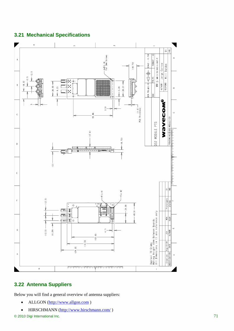
Omni Product Technical Specification
© 2010 Digi International Inc. 71
3.21 Mechanical Specifications
3.22 Antenna Suppliers
Below you will find a general overview of antenna suppliers:
• ALLGON (http://www.allgon.com )
• HIRSCHMANN (http://www.hirschmann.com/ )

Omni Product Technical Specification
© 2010 Digi International Inc. 72
Orbcomm antennas and support can be obtained from suppliers such as
• HIRSCHMANN (http://www.hirschmann.com/ )
• INEVITABLE TECHNOLOGIES (http://www.inevtech.com/orbcomm-antennas)
• LAIRD TECHNOLOGIES (http://www.lairdtech.com)
• MULTIBAND ANTENNAS LIMITED (http://www.multiband-antennas.com)
Please note that all suppliers listed are for general reference only. Other antenna suppliers are available.
Spectrum Design Solutions, a wholly owned subsidiary of Digi International, offers complete software and wireless
antenna design services for the Digi m130 based products.
Online www.spectrumdsi.com E-Mail [email protected]
Phone +1 612-435-0789
.
Omni Product Technical Specification
© 2010 Digi International Inc. 73
Appendix
3.23 Standards and Recommendations
GSM ETSI, 3GPP, GCF and NAPRD03 recommendations for Phase II & FCC.
Specification Reference Title
3GPP TS 45.005 v5.5.0 (2002-08) Release 5
Technical Specification Group GSM/EDGE. Radio Access Network; Radio transmission and reception
GSM 02.07 V8.0.0 (1999-07)
Digital cellular telecommunications system (Phase 2+);
Mobile Stations (MS) features (GSM 02.07 version 8.0.0 Release 1999)
GSM 02.60 V8.1.0 (1999-07)
Digital cellular telecommunications system (Phase 2+);
General Packet Radio Service (GPRS); Service description, Stage 1 (GSM 02.60 version 8.1.0 Release 1999)
GSM 03.60 V7.9.0 (2002-09)
Technical Specification Group Services and System Aspects;
Digital cellular telecommunications system (Phase 2+); General Packet Radio Service (GPRS); Service description; Stage 2 (Release 1998)
3GPP TS 43.064 V5.0.0 (2002-04) Technical Specification Group GERAN; Digital cellular telecommunications system (Phase 2+); General Packet Radio Service (GPRS); Overall description of the GPRS radio interface; Stage 2 (Release 5)
3GPP TS 03.22 V8.7.0 (2002-08) Technical Specification Group GSM/EDGE. Radio Access Network; Functions related to Mobile Station (MS) in idle mode and group receive mode; (Release 1999)
3GPP TS 03.40 V7.5.0 (2001-12)
Technical Specification Group Terminals;
Technical realization of the Short Message Service (SMS)
(Release 1998)
3GPP TS 03.41 V7.4.0 (2000-09) Technical Specification Group Terminals; Technical realization of Cell Broadcast Service (CBS) (Release 1998)
ETSI EN 300 903 V8.1.1 (2000-11)
Digital cellular telecommunications system (Phase 2+);
Transmission planning aspects of the speech service in the GSM
Public Land Mobile Network (PLMN) system (GSM 03.50 version 8.1.1 Release 1999)
Omni Product Technical Specification
© 2010 Digi International Inc. 74
Specification Reference Title 3GPP TS 04.06 V8.2.1 (2002-05) Technical Specification Group GSM/EDGE Radio Access Network;
Mobile Station - Base Station System (MS - BSS) interface; Data Link (DL) layer specification (Release 1999)
3GPP TS 04.08 V7.18.0 (2002-09) Technical Specification Group Core Network;
Digital cellular telecommunications system (Phase 2+);
Mobile radio interface layer 3 specification (Release 1998)
3GPP TS 04.10 V7.1.0 (2001-12)
Technical Specification Group Core Networks;
Mobile radio interface layer 3 Supplementary services specification; General aspects (Release 1998)
3GPP TS 04.11 V7.1.0 (2000-09) Technical Specification Group Core Network; Digital cellular telecommunications system (Phase 2+); Point-to-Point (PP) Short Message Service (SMS) support on mobile radio interface
(Release 1998)
3GPP TS 45.005 v5.5.0 (2002-08) Technical Specification Group GSM/EDGE. Radio Access Network; Radio transmission and reception (Release 5)
3GPP TS 45.008 V5.8.0 (2002-08) Technical Specification Group GSM/EDGE
Radio Access Network; Radio subsystem link control (Release 5)
3GPP TS 45.010 V5.1.0 (2002-08) Technical Specification Group GSM/EDGE
Radio Access Network; Radio subsystem synchronization (Release 5)
3GPP TS 46.010 V5.0.0 (2002-06) Technical Specification Group Services and System Aspects;
Full rate speech; Transcoding (Release 5)
3GPP TS 46.011 V5.0.0 (2002-06) Technical Specification Group Services and System Aspects;
Full rate speech; Substitution and muting of lost frames for
full rate speech channels (Release 5)
3GPP TS 46.012 V5.0.0 (2002-06) Technical Specification Group Services and System Aspects;
Full rate speech; Comfort noise aspect for full rate speech traffic channels (Release 5)
Omni Product Technical Specification
© 2010 Digi International Inc. 75
Specification Reference Title 3GPP TS 46.031 V5.0.0 (2002-06)
Technical Specification Group Services and System Aspects;
Full rate speech; Discontinuous Transmission (DTX) for full rate speech traffic channels (Release 5)
3GPP TS 46.032 V5.0.0 (2002-06) Technical Specification Group Services and System Aspects;
Full rate speech; Voice Activity Detector (VAD) for full rate speech traffic channels (Release 5)
TS 100 913V8.0.0 (1999-08)
Digital cellular telecommunications system (Phase 2+);
General on Terminal Adaptation Functions (TAF) for Mobile Stations (MS) (GSM 07.01 version 8.0.0 Release 1999)
GSM 09.07 V8.0.0 (1999-08)
Digital cellular telecommunications system (Phase 2+);
General requirements on interworking between the Public Land Mobile Network (PLMN) and the Integrated Services Digital Network (ISDN) or Public Switched Telephone Network (PSTN) (GSM 09.07 version 8.0.0 Release 1999)
3GPP TS 51.010-1 v5.0.0 (2002-09)
Technical Specification Group GSM/EDGE ; Radio Access Network ;Digital cellular telecommunications system (Phase 2+);Mobile Station (MS) conformance specification; Part 1: Conformance specification (Release 5)
3GPP TS 51.011 V5.0.0 (2001-12) Technical Specification Group Terminals; Specification of the Subscriber Identity Module - Mobile Equipment (SIM - ME) interface (Release 5)
ETS 300 641 (1998-03) Digital cellular telecommunications system (Phase 2);
Specification of the 3 Volt Subscriber Identity Module - Mobile Equipment (SIM-ME) interface (GSM 11.12 version 4.3.1)
GCF-CC V3.7.1 (2002-08) Global Certification Forum – Certification criteria
NAPRD03 V2.6.0 (2002-06) North America Permanent Reference Document for PTCRB tests
The Digi m130 connected on a development kit board application is certified to be in accordance with the following Rules and Regulations of the Federal Communications Commission (FCC). Power listed on the Grant is conducted for Part 22 and conducted for Part 24
Omni Product Technical Specification
© 2010 Digi International Inc. 76
This device contains GSM, GPRS Class 10 functions in the 900 and 1800MHz Band which are not operational in U.S. Territories. This device is to be used only for mobile and fixed applications. The antenna(s) used for this transmitter must be installed to provide a separation distance of at least 20cm from all persons and must not be co-located or operating in conjunction with any other antenna or transmitter. Users and installers must be provided with antenna installation instructions and transmitter operating conditions for satisfying RF exposure compliance. Antennas used for this OEM module must not exceed 3.1dBi gain for PCS 1900 MHz and 0.9dBi for GSM 850 MHz for mobile and fixed operating configurations. This device is approved as a module to be installed in other devices. Installed in other portable devices, the exposure conditions require a separate equipment authorization. The license module had a FCC ID label on the module itself. The FCC ID label must be visible through a window or it must be visible when an access panel, door or cover is easily removed. If not, a second label must be placed on the outside of the device that contains the following text: Contains FCC ID: O9EQ52OMNI This device complies with Part 15 of the FCC Rules. Operation is subject to the following two conditions:
(1) this device may not cause harmful interference, (2) this device must accept any interference received, including interference that may cause undesired
operation. IIMPORTANT: Manufacturers of mobile or fixed devices incorporating the Digi m130 device are advised to: • clarify any regulatory questions, • have their completed product tested, • have product approved for FCC compliance, and • include instructions according to above mentioned RF exposure statements in end product user manual.
Please note that changes or modifications not expressly approved by the party responsible for compliance could void the user’s authority to operate the equipment.
Omni Product Technical Specification
© 2010 Digi International Inc. 77
3.24 Declaration of Conformity
To Whom it May Concern:
We,Wavecom
430 Davis Drive Suite 300
PO Box 13920
Research Triangle Park
NC 27709 USA
declare under our sole responsibility that the Product
Digi m130
to which this declaration relates is in conformity with the following standards or other normative documents
EN 301 721
EN 301-489-20
as they apply to the above referenced Product.
Research Triangle Park
November 12, 2008
Peter Cotterill
Certification Manager

Omni Product Technical Specification
© 2010 Digi International Inc. 78
3.25 Safety Recommendations (for Information Only)
IMPORTANT
FOR THE EFFICIENT AND SAFE OPERATION OF YOUR GSM APPLICATION
PLEASE READ THIS INFORMATION CAREFULLY
3.25.1 RF Safety
3.25.1.1 General Your GSM terminal*
Your GSM terminal is actually a low power radio transmitter and receiver. It sends out and receives radio frequency energy. When you use your GSM application, the cellular system which handles your calls controls both the radio frequency and the power level of your cellular modem.
is based on the GSM standard for cellular technology. The GSM standard is spread all over the world. It covers Europe, Asia and some parts of America and Africa. This is the most used telecommunication standard.
3.25.1.2 Exposure to RF Energy There has been some public concern about possible health effects of using GSM terminals. Although research on health effects from RF energy has focused on the current RF technology for many years, scientists have begun research regarding newer radio technologies, such as GSM. After existing research had been reviewed, and after compliance to all applicable safety standards had been tested, it has been concluded that the product was fitted for use.
If you are concerned about exposure to RF energy there are things you can do to minimize exposure. Obviously, limiting the duration of your calls will reduce your exposure to RF energy. In addition, you can reduce RF exposure by operating your cellular terminal efficiently by following the guidelines below.
3.25.1.3 Efficient Terminal Operation For your GSM terminal to operate at the lowest power level, consistent with satisfactory call quality:
If your terminal has an extendable antenna, extend it fully. Some models allow you to place a call with the antenna retracted. However your GSM terminal operates more efficiently with the antenna fully extended.
Do not hold the antenna when the terminal is "IN USE". Holding the antenna affects call quality and may cause the modem to operate at a higher power level than needed.
3.25.1.4 Antenna Care and Replacement Do not use the GSM terminal with a damaged antenna. If a damaged antenna comes into contact with the skin, a minor burn may result. Replace a damaged antenna immediately. Consult your manual to see if you may change the antenna yourself. If so, use only a manufacturer-approved antenna. Otherwise, have your antenna repaired by a qualified technician.
Use only the supplied or approved antenna. Unauthorized antennas, modifications or attachments could damage the terminal and may contravene local RF emission regulations or invalidate type approval.
* based on WISMO2D

Omni Product Technical Specification
© 2010 Digi International Inc. 79
3.25.2 General Safety
3.25.2.1 Driving Check the laws and the regulations regarding the use of cellular devices in the area where you have to drive as you always have to comply with them. When using your GSM terminal while driving, please:
give full attention to driving,
pull off the road and park before making or answering a call if driving conditions so require.
3.25.2.2 Electronic Devices Most electronic equipment, for example in hospitals and motor vehicles is shielded from RF energy. However RF energy may affect some improperly shielded electronic equipment.
3.25.2.3 Vehicle Electronic Equipment Check your vehicle manufacturer representative to determine if any on-board electronic equipment is adequately shielded from RF energy.
3.25.2.4 Medical Electronic Equipment Consult the manufacturer of any personal medical devices (such as pacemakers, hearing aids, etc...) to determine if they are adequately shielded from external RF energy.
Turn your terminal OFF in health care facilities when any regulations posted in the area instruct you to do so. Hospitals or health care facilities may be using RF monitoring equipment.

Omni Product Technical Specification
© 2010 Digi International Inc. 80
3.25.2.5 Aircraft Turn your terminal OFF before boarding any aircraft.
Use it on the ground only with crew permission.
Do not use it in the air.
To prevent possible interference with aircraft systems, Federal Aviation Administration (FAA) regulations require you to have permission from a crew member to use your terminal while the aircraft is on the ground. To prevent interference with cellular systems, local RF regulations prohibit using your modem while airborne.
3.25.2.6 Children Do not allow children to play with your GSM terminal. It is not a toy. Children could hurt themselves or others (by poking themselves or others in the eye with the antenna, for example). Children could damage the modem, or make calls that increase your modem bills.
3.25.2.7 Blasting Areas To avoid interfering with blasting operations, turn your unit OFF when in a "blasting area" or in areas posted: "turn off two-way radio". Construction crew often uses remote control RF devices to set off explosives.
3.25.2.8 Potentially Explosive Atmospheres Turn your terminal OFF when in any area with a potentially explosive atmosphere. It is rare, but your modem or its accessories could generate sparks. Sparks in such areas could cause an explosion or fire resulting in bodily injuries or even death.
Areas with a potentially explosive atmosphere are often, but not always, clearly marked. They include fueling areas such as petrol stations; below decks on boats; fuel or chemical transfer or storage facilities; and areas where the air contains chemicals or particles, such as grain, dust, or metal powders.
Do not transport or store flammable gas, liquid, or explosives, in the compartment of your vehicle which contains your terminal or accessories.
Before using your terminal in a vehicle powered by liquefied petroleum gas (such as propane or butane) ensure that the vehicle complies with the relevant fire and safety regulations of the country in which the vehicle is to be used.