Embed Size (px)
Citation preview
1 | P a g e
V S M COLLEGE OF ENGINEERING
LECTURE NOTES
ON
DIGITAL DESIGN USING VERILOG HDL
IV B.Tech I semester (JNTUK-R16)
ELECTRONICS AND COMMUNICATION ENGINEERING
2 | P a g e
V S M COLLEGE OF ENGINEERING
UNIT - 1
SYLLABUS:
INTRODUCTION TO VERILOG: Verilog as HDL, Levels of design Description, Concurrency, Simulation and Synthesis, Functional
Verification, System Tasks, Programming Language Interface (PLI), Module, Simulation and Synthesis
Tools, Test Benches.
LANGUAGE CONSTRUCTS AND CONVENTIONS:
Introduction, Keywords, Identifiers, White Space Characters, Comments, Numbers, Strings, Logic Values,
Strengths, Data Types, Scalars and Vectors, Parameters, Operators. --------------------------------------------------------------------------------------------------------------------------------
INTRODUCTION TO VERILOG:
VERILOG AS AN HDL
Verilog aimed at providing a functionally tested and a verified design description for the target FPGA or
ASIC. The language has a dual function – one fulfilling the need for a design description and the other fulfilling the need for verifying the design for functionality and timing constraints like propagation delay,
critical path delay, slack, setup, and hold times
LEVELS OF DESIGN DESCRIPTION
1. Circuit Level: At the circuit level, a switch is the basic element with which digital circuits are built. Switches can be
combined to form inverters and other gates at the next higher level of abstraction. Verilog has the basic
MOS switches built into its constructs, which can be used to build basic circuits like inverters, basic logic gates, simple 1-bit dynamic and static memories
3 | P a g e
V S M COLLEGE OF ENGINEERING
2. Gate Level :-
At the next higher level of abstraction, design is carried out in terms of basic gates. All the basic gates are
available as ready modules called ―Primitives.‖ Each such primitive is defined in terms of its inputs and outputs. Primitives can be incorporated into design descriptions directly.
3. Data Flow :- Data flow is the next higher level of abstraction. All possible operations on signals and variables are
represented here in terms of assignments. All logic and algebraic operations are accommodated. The
assignments define the continuous functioning of the concerned block. At the data flow level, signals are assigned through the data manipulating equations. All such assignments are concurrent in nature. The
design descriptions are more compact than those at the gate level.
4. Behavioral Level :-
Behavioral level constitutes the highest level of design description; it is essentially at the system level itself. With the assignment possibilities, looping constructs and conditional branching possible, the design
description essentially looks like a ―C‖ program.
CONCURRENCY
In an electronic circuit all the units are to be active and functioning concurrently. The voltages and
currents in the different elements in the circuit can change simultaneously. In turn the logic levels too can change. Simulation of such a circuit in an HDL calls for concurrency of operation. Verilog simulators are
built to simulate concurrency.
SIMULATION AND SYNTHESIS
The design that is specified and entered as described is simulated for functionality and fully debugged. Translation of the debugged design into the corresponding hardware circuit (using an FPGA or an ASIC)
is called ―synthesis‖. The circuits realized from them are essentially direct translations of functions into
circuit elements.
FUNCTIONAL VERIFICATION
Testing is an essential ingredient of the VLSI design process as with any hardware circuit. It has two dimensions to it – functional tests and timing tests. Testing or functional verification is carried out by
setting up a ―test bench‖ for the design. The test bench will have the design instantiated in it; it will
generate necessary test signals and apply them to the instantiated design.
4 | P a g e
V S M COLLEGE OF ENGINEERING
Test Inputs for Test Benches:
Any digital system has to carry out a number of activities in a defined manner. Once a proper design is done, it has to be tested for all its functional aspects. Test inputs can be purely combinational, periodic,
numeric sequences, random inputs, conditional inputs, or combinations of these. As the circuit design
proceeds, one develops smaller blocks and groups them together to form bigger circuit units. The process is repeated until the whole system is fully built up. Every stage calls for tests to see whether the subsystem
at that layer behaves in the manner expected.
Such testing calls for two types of observations: Study of signals within a small unit when test inputs are given to the whole unit.
Isolation of a small element and doing local test to facilitate debugging.
Constructs for Modeling Timing Delays:
Any basic gate has propagation delays and transmission delays associated with it. As the elements in the
circuit increase in number, the type and variety of such delays increase rapidly; often one reaches a stage
where the expected function is not realized thanks to an unduly large time delay.
Verilog has constructs for modeling the following delays: Gate delay
Net delay Path delay
Pin-to-pin delay A design can be tested for setup time, hold time, clock-width time specifications, etc. Such constructs or delay models are akin to the finite delay time, rise time, fall time, path or propagation delays, etc.,
associated with real digital circuits or systems. The use of such constructs in the design helps simulate
realistic conditions in a digital circuit.
SYSTEM TASKS
A number of system tasks are available in Verilog. Though used in a design description, they are not part
of it. Some tasks facilitate control and flow of the testing process. Reading data from specified files into a
module and writing back into files are also possible through other tasks. Timescale can be changed prior to simulation with the help of specific tasks for the purpose.
A set of system functions add to the flexibility of test benches: They are of three categories:
Functions that keep track of the progress of simulation time
Functions to convert data or values of variables from one format to another Functions to generate random numbers with specific distributions
PROGRAMMING LANGUAGE INTERFACE (PLI)
PLI provides an active interface to a compiled Verilog module. The interface adds a new dimension to
working with Verilog routines from a C platform.
The key functions of the interface are as follows: One can read data from a file and pass it to a Verilog module as input. Such data can be test vectors or
other input data to the module. Similarly, variables in Verilog modules can be accessed and their values
written to output devices.
Delay values, logic values, etc., within a module can be accessed and altered. Blocks written in C language can be linked to Verilog modules.
5 | P a g e
V S M COLLEGE OF ENGINEERING
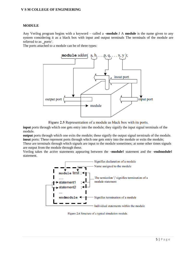
MODULE
Any Verilog program begins with a keyword – called a ―module.‖ A module is the name given to any
system considering it as a black box with input and output terminals The terminals of the module are
referred to as ‗ports‘.
The ports attached to a module can be of three types:
input ports through which one gets entry into the module; they signify the input signal terminals of the
module.
output ports through which one exits the module; these signify the output signal terminals of the module. inout ports: These represent ports through which one gets entry into the module or exits the module;
These are terminals through which signals are input to the module sometimes; at some other times signals
are output from the module through these.
Verilog takes the active statements appearing between the ―module‖ statement and the ―endmodule‖ statement.
6 | P a g e
V S M COLLEGE OF ENGINEERING
SIMULATION AND SYNTHESIS TOOLS
A variety of Software tools related to VLSI design is available. We discuss here two of them directly
relevant to us – Modelsim and Leonardo Spectrum of Mentor Graphics. Modelsim has been used to simulate the designs. Simulation results presented for the variety of examples discussed in the book have
been obtained using it. Leonardo Spectrum has been used to obtain the synthesized circuits presented. We
would like to draw the attention of the readers to the following in this context:
� Only the essential aspects of the tools are presented – those essential for the progress of the book.
� For more details of the tools and the variety of facilities they offer, one can refer to the respective user manuals and the Help menus.
� Tools from other sources are similar in essentials. Any of them can be used.
Modelsim SE 5.5
Synthesis
TEST BENCHES
Any digital circuit that has been designed and wired goes through a testing process before being declared
as ready for use. Testing involves studying circuit behavior under simulated conditions for the following:
� Check and ensure that all functions are carried out as desired. It is the test for the static behavior of the circuit. A set of logic input values are applied at selected points and the logic values at another set of
points observed.
� Check and ensure that all the functional sequences are carried out as desired. It is one of the tests for the
dynamic behavior of the circuit. It may call for the generation of specific input sequences with respect to time, applying them to the circuit and observing selected outputs.
� Check for the timing behavior: One tests for the propagation and other types of delays here. A variety of
tests may have to be carried out. It may involve observation of variations in the signals at selected points,
measuring the time delay between specified events, measuring pulse widths, and so on.
LANGUAGE CONSTRUCTS AND CONVENTIONS:
INTRODUCTION
The constructs and conventions make up a software language. A clear understanding and familiarity of
these is essential for the mastery of the language. Verilog has its own constructs and conventions [IEEE,
Sutherland]. In many respects they resemble those of C language [Gottfried]. We discuss the constructs and conventions essential to the progress of the book.
Case Sensitivity
Verilog is a case-sensitive language like C. Thus sense, Sense, SENSE, sENse,… etc., are all treated as different entities / quantities in Verilog.
KEYWORDS
The keywords define the language constructs. A keyword signifies an activity to be carried out, initiated,
or terminated. As such, a programmer cannot use a keyword for any purpose other than that it is intended
for. All keywords in Verilog are in small letters and require to be used as such (since Verilog is a casesensitive language). All keywords appear in the text in New Courier Bold-type letters.
Examples
module � signifies the beginning of a module definition.
endmodule � signifies the end of a module definition. begin � signifies the beginning of a block of statements.
7 | P a g e
V S M COLLEGE OF ENGINEERING
end � signifies the end of a block of statements.
if � signifies a conditional activity to be checked
while � signifies a conditional activity to be carried out.
IDENTIFIERS
Any program requires blocks of statements, signals, etc., to be identified with an attached nametag. Such
nametags are identifiers. It is good practice for us to use identifiers, closely related to the significance of variable, signal, block, etc., concerned. This eases understanding and debugging of any program.
e.g., clock, enable, gate_1, . . .
There are some restrictions in assigning identifier names. All characters of the alphabet or an underscore
can be used as the first character. Subsequent characters can be of alphanumeric type, or the underscore
(_), or the dollar ($) sign – for example
name, _name. Name, name1, name_$, . . . � all these are allowed as identifiers name aa � not allowed as an identifier because of the blank ( ―name‖ and ―aa‖ are interpreted as two
different identifiers)
$name � not allowed as an identifier because of the presence of ―$‖ as the first character.
1_name � not allowed as an identifier, since the numeral ―1‖ is the first character
@name � not allowed as an identifier because of the presence of the character ―@‖.
A+b � not allowed as an identifier because of the presence of the character ―+‖ .
WHITE SPACE CHARACTERS Blanks (\b), tabs (\t), newlines (\n), and form feed form the white space characters in Verilog. In any
design description the white space characters are included to improve readability. Functionally, they
separate legal tokens. They are introduced between keywords, keyword and an identifier, between two identifiers, between identifiers and operator symbols, and so on. White space characters have significance
only when they appear inside strings.
COMMENTS It is a healthy practice to comment a design description liberally – as with any other program. Comments
are incorporated in two ways. A single line comment begins with ―//‖ and ends with a new line – for
example
module d_ff (Q, dp, clk); //This is the design description of a D flip-flop.
//Here Q is the output.
// dp is the input and clk is the clock.
One can incorporate multiline comments also without resorting to ―//‖ at every line. For such multiline
comments ―/*‖ signifies the beginning of a comment and ―*/‖ its end. All lines appearing between these
two symbol combinations are together treated as a single block comment – for example
module d_ff (Q, dp, clk);
/* This module forms the design description of a d_flip_flop wherein
Q is the output of the flip-flop ,
dp is the data input and clk the clock input*/
8 | P a g e
V S M COLLEGE OF ENGINEERING
NUMBERS
Frequently numbers need to be specified in a design description. Logic status of signal lines, buses, delay
values, and numbers to be loaded in registers are examples. The numbers can be of integer type or real type.
1. Integer Numbers 2. Real Numbers
STRINGS
A string is a sequence of characters enclosed within double quotes. A string must be contained on a single line; that is, it cannot be carried over to two lines with a carriage return. Special characters are specified by
preceding them with the ―\‖ character. Verilog treats a string as a sequence of ASCII characters – for
example,
―This is a string‖
―This string is one \t with a gap in between‖ ―This is called a \―string\‖‖.
When a string of ASCII characters as above is an operand in an expression, it is treated as a binary
number. This binary number is formed by replacing each ASCII character by 8 bits – a 0 bit followed by the 7-bit ASCII equivalent – and treating the resulting binary sequence as a single binary number. For
example, the statement (with P defined as a 32-bit vector beforehand)
P = ―numb‖
assigns the binary value
0110 1110 0111 0101 0110 1101 0110 0010 to P (0110 1110, 0111 0101, 0110 1101 and 0110 0010 are the 8-bit equivalents
of the letters n, u, m, and b, respectively).
LOGIC VALUES Signal lines, logic values appearing on signal lines, etc., can normally take two logic levels: 1 � signifies the 1 or high or true level
0 � signifies the 0 or low or false level.
Two additional levels are also possible – designated as x and z. Here x represents an unknown or an
uninitialized value. This corresponds to the don‘t care case in logic circuits. z represents / signifies a high
impedance state. This is possible when a signal line is tri-stated or left floating. The following are
note worthy here: � When a variable in an expression is in the z state, the effect is the same as it having z value. But when
an input to a gate is in the z state, it is equivalent to having the x value.
� The MOS switches discussed in Chapter 10 form an exception to the above. If the input to a MOS switch is in the z state, its output too remains at the z state.
� With a few exceptions all data types in Verilog can take on all the 4 logic values or levels. The event is
an exception to this. It cannot store any value. The trireg cannot take on the z value
STRENGTHS
The logic levels are also associated with strengths. In many digital circuits, multiple assignments are often combined to reduce silicon area or to reduce pinouts. To facilitate this, one can assign strengths to logic
levels. Verilog has eight strength levels – four of these are of the driving type, three are of capacitive type
and one of the hi-Z type. When a signal line is driven simultaneously from two sources of different strength levels, the stronger of
the two prevails. A few illustrative examples are considered here.
� If a signal line a is driven by two sources – b at 1 level with strength ―strong1‖ and c at level 0 with
strength ―pull0‖– a will take the value 1.
9 | P a g e
V S M COLLEGE OF ENGINEERING
� If a signal line a is driven by two sources – b at 1 level with strength ―pull1‖ and c at level 0 with strength ―strong0,‖ a will take the value 0.
� If a signal line a is driven by two sources – b at 1 level with strength ―strong1‖ and c at level 0 with
strength ―strong0,‖ a will take the value x (indeterminate).
� If a signal line a is driven by two sources – b at 1 level with strength ―weak1‖ and c at level 0 with
strength ―large0,‖ a will take the value 0. (Note that large signifies a capacitive drive on a tri-stated line whereas weak signifies a gate / assigned output drive with a high source impedance; despite this, due to
the higher strength level, the large signal prevails.)
DATA TYPES
The data handled in Verilog fall into two categories:
(i) Net data type
(ii) Variable data type The two types differ in the way they are used as well as with regard to their respective hardware structures.
Data type of each variable or signal has to be declared prior to its use. The same is valid within the
concerned block or module.
Nets
A net signifies a connection from one circuit unit to another. Such a net carries the value of the signal it is
connected to and transmits to the circuit blocks connected to it. If the driving end of a net is left floating,
the net goes to the high impedance state. A net can be specified in different ways.
wire: It represents a simple wire doing an interconnection. Only one output is connected to a wire and is driven by that.
tri: It represents a simple signal line as a wire. Unlike the wire, a tri can be driven by more than one signal
outputs.
Functionally, wire and tri are identical. Distinct nomenclatures are provided for the convenience of assigning roles.
Variable Data Type
A variable is an abstraction for a storage device. It can be declared through the keyword reg and stores the value of a logic level: 0, 1, x, or z. A net or wire connected to a reg takes on the value stored in the reg
and can be used as input to other circuit elements. But the output of a circuit cannot be connected to a reg.
The value stored in a reg is changed through a fresh assignment in the program. time, integer, real, and
realtime are the other variable types of data; these are dealt with later.
SCALARS AND VECTORS
Entities representing single bits — whether the bit is stored, changed, or transferred — are called ―scalars.‖ Often multiple lines carry signals in a cluster – like data bus, address bus, and so on. Similarly, a
group of regs stores a value, which may be assigned, changed, and handled together. The collection here is
treated as a ―vector.‖ Below figure illustrates the difference between a scalar and a vector. wr and rd are two scalar nets connecting two circuit blocks circuit1 and circuit2. b is a 4-bit-wide vector net connecting
the same two blocks. b[0], b[1], b[2], and b[3] are the individual bits of vector b. They are ―part vectors.‖
A vector reg or net is declared at the outset in a Verilog program and hence treated as such. The range of a vector is specified by a set of 2 digits (or expressions evaluating to a digit) with a colon in between the
two. The combination is enclosed within square brackets.
10 | P a g e
V S M COLLEGE OF ENGINEERING
wire[3:0] a; /* a is a four bit vector of net type; the bits are designated as a[3], a[2], a[1] and a[0]. */
reg[2:0] b; /* b is a three bit vector of reg type; the bits are designated as b[2], b[1] and b[0]. */
reg[4:2] c; /* c is a three bit vector of reg type; the bits are designated as c[4], c[3] and c[2]. */
wire[-2:2] d ; /* d is a 5 bit vector with individual bits designated as d[-2], d[-1], d[0], d[1] and d[2]. */
Whenever a range is not specified for a net or a reg, the same is treated as a scalar – a single bit quantity. In the range specification of a vector the most significant bit and the least significant bit can be assigned
specific integer values. These can also be expressions evaluating to integer constants – positive or
negative. Normally vectors – nets or regs – are treated as unsigned quantities. They have to be specifically
declared as ―signed‖ if so desired.
Examples
wire signed[4:0] num; // num is a vector in the range -16 to +15. reg signed [3:0] num_1; // num_1 is a vector in the range -8 to +7.
PARAMETERS
In some designs, certain parameter values are not committed at the outset. Proportionality constants, frequency-scaling levels, number of taps in digital filters, etc., are typical examples. There are also
situations where the size of the design is left open and decided at a later stage. Bus width, LIFO depth, and
memory size are such quantities which may be committed later. All such constants can be declared as parameters at the outset in a Verilog module, and values can be assigned to them; for example,
parameter word_size = 16;
parameter word_size = 16, mem_size = 256;
Such parameter assignments are made at compiler time. The parameter values cannot be changed
(normally) at runtime. However, a parameter that has been assigned a value in a module definition can
have its value changed at runtime – that is, when the module is used at runtime in some other design (i.e.,
instantiated) or when it is tested. Such modifications are carried out through a ―defparameter‖ statement. The parameter assignment done as part of parameter declaration can have the appropriate constant on the
right-hand side of the assignment statement, as was the case above. The assignment can also have
11 | P a g e
V S M COLLEGE OF ENGINEERING
algebraic expressions on the right hand side. Such expressions can involve constants and other parameters declared already; for example
Parameter word_size = 16, factor = word_size/2;
OPERATORS
Verilog has a number of operators akin to the C language. These are of three types:
1. Unary: the unary operator is associated with a single operand. The operator precedes the operand – for
example, ~a.
2. Binary: the binary operator is associated with two operands. The operator appears between the two operands – for example, a&b.
3. Ternary: the ternary operator is associated with three operands. The two operators together constitute a
ternary operation. The two operators separate the three operands – for example a?b:c // Here the operators
―?‖ and ―:‖ together define an operation.
12 | P a g e
V S M COLLEGE OF ENGINEERING
UNIT - II
SYLLABUS:
GATE LEVEL MODELING
AND Gate Primitive, Module Structure, Other Gate Primitives, Illustrative Examples, Tri-State Gates,
Array of Instances of Primitives, Design of Flip-flops with Gate Primitives, Delays, Strengths and
Contention Resolution, Net Types, Design of Basic Circuits.
MODELING AT DATA FLOW LEVEL
Introduction, Continuous assignment structures, Delays and continuous, Assignments, Assignment to
vectors, Operators
--------------------------------------------------------------------------------------------------------------------------------
MODULE STRUCTURE
The first statement of a module starts with the keyword module; it may be followed by the name
of the module and the port list if any. All the variables in the ports-list are to be identified as inputs,
outputs, or inouts.
The corresponding declarations have the form shown below:
Input a1, a2;
Output b1, b2;
Inout c1, c2;
The port-type declarations here follow the module declaration mentioned above. The ports and the
other variables used within the body of the module are to be identified as nets or registers with specific
types in each case.
The respective declaration statements follow the port-type declaration statements.
Examples: wire a1, a2, c;
reg b1, b2;
The type declaration must necessarily precede the first use of any variable or signal in the module.
The executable body of the module follows the declaration indicated above.
The last statement in any module definition is the keyword ―endmodule‖. Comments can appear anywhere
in the module definition.
AND GATE PRIMITIVE
The AND gate primitive in Verilog is instantiated with the following statement:
and g1 (O, I1, I2, . . ., In);
The AND module has only one output. The first port in the argument list is the output port.
An AND gate instantiation can take any number of inputs — the upper limit is compiler-specific. A name need not be necessarily assigned to the AND gate instantiation; this is true of all the gate
primitives available in Verilog.
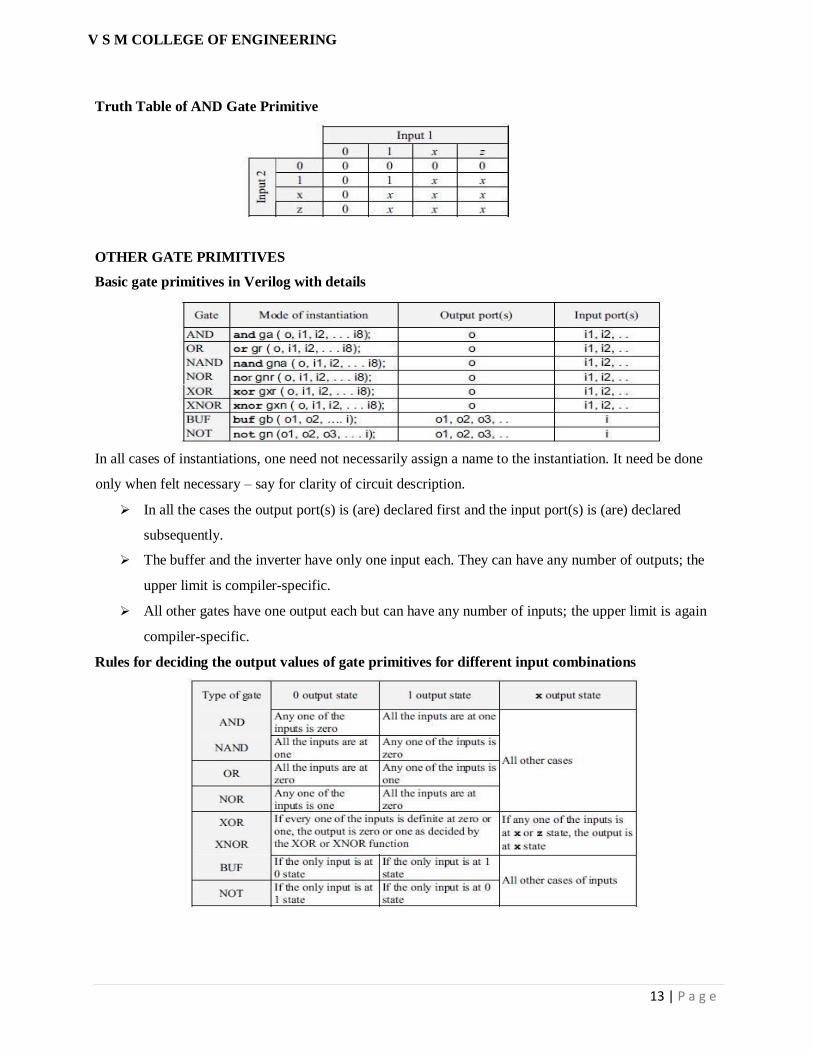
13 | P a g e
V S M COLLEGE OF ENGINEERING
Truth Table of AND Gate Primitive
OTHER GATE PRIMITIVES
Basic gate primitives in Verilog with details
In all cases of instantiations, one need not necessarily assign a name to the instantiation. It need be done
only when felt necessary – say for clarity of circuit description.
In all the cases the output port(s) is (are) declared first and the input port(s) is (are) declared
subsequently.
The buffer and the inverter have only one input each. They can have any number of outputs; the
upper limit is compiler-specific.
All other gates have one output each but can have any number of inputs; the upper limit is again
compiler-specific.
Rules for deciding the output values of gate primitives for different input combinations
14 | P a g e
V S M COLLEGE OF ENGINEERING
Example programs
EX 2-to-4 Decoder
module dec2_4 (a,b,en);
output [3:0] a; input [1:0]b; input en; wire [1:0]bb; not(bb[1],b[1]),(bb[0],b[0]);
and(a[0],en, bb[1],bb[0]),(a[1],en, bb[1],b[0]),(a[2],en, b[1],bb[0]),(a[3],en,
b[1],b[0]);
endmodule
//test bench module
tst_dec2_4();
wire [3:0]a;
reg[1:0] b; reg en;
dec2_4 dec(a,b,en);
initial
initial
begin
end
{b,en} =3'b000;
#2{b,en} =3'b001;
#2{b,en} =3'b011;
#2{b,en} =3'b101;
#2{b,en} =3'b111;
$monitor ($time , "output a = %b, input b = %b ", a, b);
endmodule
TRI-STATE GATES
A tri-state buffer
15 | P a g e
V S M COLLEGE OF ENGINEERING
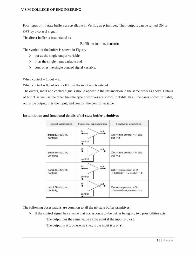
Four types of tri-state buffers are available in Verilog as primitives. Their outputs can be turned ON or
OFF by a control signal.
The direct buffer is instantiated as
Bufif1 nn (out, in, control);
The symbol of the buffer is shown in Figure.
out as the single output variable
in as the single input variable and
control as the single control signal variable.
When control = 1, out = in.
When control = 0, out is cut off from the input and tri-stated.
The output, input and control signals should appear in the instantiation in the same order as above. Details
of bufif1 as well as the other tri-state type primitives are shown in Table. In all the cases shown in Table,
out is the output, in is the input, and control, the control variable.
Instantiation and functional details of tri-state buffer primitives
The following observations are common to all the tri-state buffer primitives:
If the control signal has a value that corresponds to the buffer being on, two possibilities exist:
The output has the same value as the input if the input is 0 or 1.
The output is at x otherwise (i.e., if the input is x or z).
16 | P a g e
V S M COLLEGE OF ENGINEERING
If the control signal has a value that corresponds to the control signal being off, the output is at z
state irrespective of the value of the input.
If the control signal is at x or z, three possibilities arise:
If the input is at x or z, the output is at x.
If the input is at 0 state, the output is L for bufif1 and bufif0. It is at H for notif1 and notif0.
If the input is at 1 state, the output is H for bufif1 and bufif0. It is at L for notif1 and notif0.
Note that H corresponds to 1 or z state while L corresponds to 0 or z state
ARRAY OF INSTANCES OF PRIMITIVES
The primitives available in Verilog can also be instantiated as arrays. A judicious use of such array
instantiations often leads to compact design descriptions.
A typical array instantiation has the form
and gate [7 : 4 ] (a, b, c); where a, b, and c are to be 4 bit vectors.
The above instantiation is equivalent to combining the following 4 instantiations:
and gate [7] (a[3], b[3], c[3]), gate [6] (a[2], b[2], c[2]), gate [5] (a[1], b[1], c[1]), gate [4] (a[0], b[0],
c[0]);
The assignment of different bits of input vectors to respective gates is implicit in the basic declaration
itself. A more general instantiation of array type has the form
and gate[mm : nn](a, b, c);
where mm and nn can be expressions involving previously defined parameters, integers and algebra with
them. The range for the gate is 1+ (mm-nn); mm and nn do not have restrictions of sign; either can be
larger than the other.
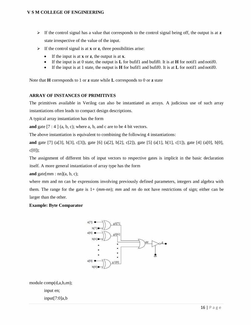
Example: Byte Comparator
module comp(d,a,b,en);
input en;
input[7:0]a,b
17 | P a g e
V S M COLLEGE OF ENGINEERING
; output d;
wire [7:0]c;
wire dd;
xor g1[7:0](c,b,a);
or(dd,c);
notif1(d,dd,en);
endmodule
Test Bench for comparator module
comp_tb;
reg[7:0]a,b; reg en; comp
gg(d,a,b,en);
initial begin a =
8'h00; b = 8'h00;
en = 1'b0;
end
always
#2 en = 1'b1;
always begin
#2 a = a+1'b1;
#2 b = b+2'd2; end
initial $monitor($time," en = %b , a = %b ,b = %b ,d = %b
",en,a,b,d); initial #30 $stop; endmodule
half adder
module ha(s,ca,a,b);
input a,b;
output s,ca;
xor(s,a,b); and(ca,a,b);
endmodule
18 | P a g e
V S M COLLEGE OF ENGINEERING
//test-bench
module tstha();
reg a,b; wire s,ca;
ha hh(s,ca,a,b);
initial begin
a=0;b=0;
end
always begin
#2 a=1;b=0;
#2 a=0;b=1;
#2 a=1;b=1;
#2 a=0;b=0; end
initial $monitor($time , " a = %b , b = %b ,out carry = %b , outsum = %b " ,a,b,ca,s);
initial #24 $stop;
endmodule
Full adder
module
fa(sum,cout,a,b,cin)
; input a,b,cin;
output sum,cout;
wire s,c1,c2;
ha ha1(s,c1,a,b), ha2(sum,c2,s,cin); or(cout,c2,c1);
19 | P a g e
V S M COLLEGE OF ENGINEERING
endmodule
//test-bench module
tst_fa();
reg a,b,cin;
fa ff(sum,cout,a,b,cin);
initial begin a
=0;b=0;cin=0;
end
always begin
#2 a=1;b=1;cin=0;#2 a=1;b=0;cin=1;
#2 a=1;b=1;cin=1;#2 a=1;b=0;cin=0;
#2 a=0;b=0;cin=0;#2 a=0;b=1;cin=0;
#2 a=0;b=0;cin=1;#2 a=0;b=1;cin=1;
#2 a=1;b=0;cin=0;#2 a=1;b=1;cin=0;
#2 a=0;b=1;cin=0;#2 a=1;b=1;cin=1;
end
initial $monitor($time ," a = %b, b = %b, cin = %b, outsum = %b, outcar = %b ",
a,b,cin,sum,cout); initial #30 $stop ;
endmodule
Mux
module mux4_1(y,i,s); input [3:0] i; input
[1:0] s; output y; wire [1:0] ss; wire
[3:0]yy; not
20 | P a g e
V S M COLLEGE OF ENGINEERING
(ss[0],s[0]),(ss[1],s[1]); and
(yy[0],i[0],ss[0],ss[1]); and
(yy[1],i[1],s[0],ss[1]); and
(yy[2],i[2],ss[0],s[1]); and
(yy[3],i[3],s[0],s[1]); or
(y,yy[3],yy[2],yy[1],yy[0]);
endmodule
//test-bench module
tst_mux4_1(); reg
[3:0]i; reg [1:0] s;
mux4_1 mm(y,i,s);
initial
begin
end
#2{i,s} = 6'b 0000_00;
#2{i,s} = 6'b 0001_00;
#2{i,s} = 6'b 0010_01;
#2{i,s} = 6'b 0100_10;
#2{i,s} = 6'b 1000_11;
#2{i,s} = 6'b 0001_00;
initial
$monitor($time," input s = %b,y = %b" ,s,y);
Endmodule
DESIGN OF FLIP-FLOPS WITH GATE PRIMITIVES
The basic RS latch can be designed using gate primitives. Two instantiations of NAND or NOR gates
suffice here.
A Simple Latch
21 | P a g e
V S M COLLEGE OF ENGINEERING
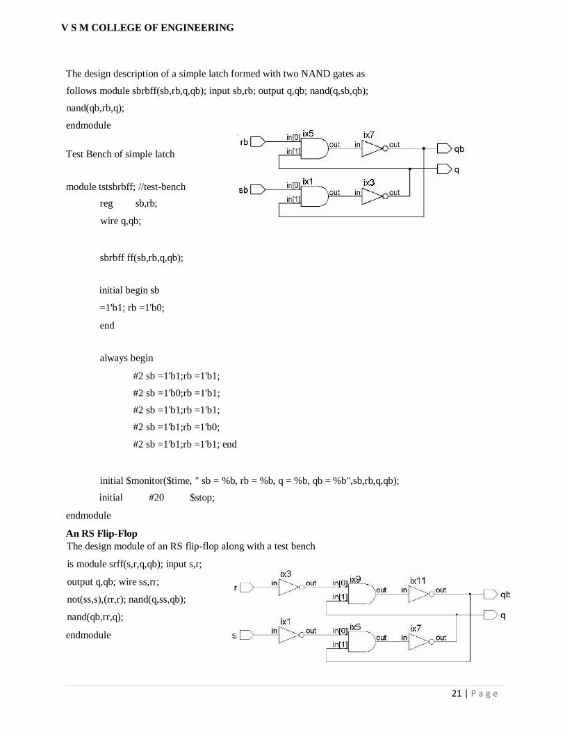
The design description of a simple latch formed with two NAND gates as
follows module sbrbff(sb,rb,q,qb); input sb,rb; output q,qb; nand(q,sb,qb);
nand(qb,rb,q);
endmodule
Test Bench of simple latch
module tstsbrbff; //test-bench
reg sb,rb;
wire q,qb;
sbrbff ff(sb,rb,q,qb);
initial begin sb
=1'b1; rb =1'b0;
end
always begin
#2 sb =1'b1;rb =1'b1;
#2 sb =1'b0;rb =1'b1;
#2 sb =1'b1;rb =1'b1;
#2 sb =1'b1;rb =1'b0;
#2 sb =1'b1;rb =1'b1; end
initial $monitor($time, " sb = %b, rb = %b, q = %b, qb = %b",sb,rb,q,qb);
initial #20 $stop;
endmodule
An RS Flip-Flop
The design module of an RS flip-flop along with a test bench
is module srff(s,r,q,qb); input s,r;
output q,qb; wire ss,rr;
not(ss,s),(rr,r); nand(q,ss,qb);
nand(qb,rr,q);
endmodule
22 | P a g e
V S M COLLEGE OF ENGINEERING
Test-Bench
module tstsrff;
reg s,r;
wire q,qb;
srff ff(s,r,q,qb);
initial begin s
=1'b1; r =1'b0;
end
always begin
#2 s =1'b0;r =1'b0;
#2 s =1'b0;r =1'b1;
#2 s =1'b0;r =1'b0;
#2 s =1'b1;r =1'b0;
#2 s =1'b0;r =1'b0; end
initial $monitor($time, " s = %b, r = %b, q = %b, qb = %b ",s,r,q,qb);
initial #20 $stop;
D-Latch
The design description of a D latch is module dlatch(en,d,q,qb); input d,en; output q,qb; wire dd;
wire s,r;
not n1(dd,d); nand (sb,d,en); nand g2(rb,dd,en);
sbrbff ff(sb,rb,q,qb);//Instantiation of the sbrbff
endmodule
Test-Bench
module tstdlatch; reg d,en; wire q,qb;
dlatch ff(en,d,q,qb);
initial begin d = 1'b0; en = 1'b0;
end
always #4 en =~en; always #8 d=~d;
23 | P a g e
V S M COLLEGE OF ENGINEERING
initial $monitor($time," en = %b , d = %b , q = %b , qb = %b " , en,d,q,qb); initial
#40 $stop;
endmodule
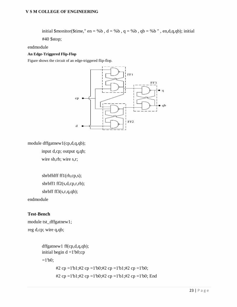
An Edge-Triggered Flip-Flop
Figure shows the circuit of an edge-triggered flip-flop.
module dffgatnew1(cp,d,q,qb);
input d,cp; output q,qb;
wire sb,rb; wire s,r;
sbrbffdff ff1(rb,cp,s);
sbrbff1 ff2(s,d,cp,r,rb);
sbrbff ff3(s,r,q,qb);
endmodule
Test-Bench
module tst_dffgatnew1;
reg d,cp; wire q,qb;
dffgatnew1 ff(cp,d,q,qb);
initial begin d =1'b0;cp
=1'b0;
#2 cp =1'b1;#2 cp =1'b0;#2 cp =1'b1;#2 cp =1'b0;
#2 cp =1'b1;#2 cp =1'b0;#2 cp =1'b1;#2 cp =1'b0; End
24 | P a g e
V S M COLLEGE OF ENGINEERING
initial
begin
#3 d=1'b1;#2d=1'b1;#2d=1'b0;#3d=1'b0;#3d=1'b1; End
initial $monitor($time," cp = %b , d = %b , q = %b , qb = %b " , cp,d,q,qb); initial
#40 $stop;
endmodule
module sbrbffdff(sb,rb,qb);
input sb,rb; output
qb; wire q;
nand(q,sb,qb);
nand(qb,rb,q);
endmodule
Test-Bench
module sbrbff1(sb,rb,cp,q,qb);
input sb,rb,cp; output
q,qb;
nand(q,sb,cp,qb);
nand(qb,rb,q); endmodule
DELAYS
Verilog has the facility to account for different types of propagation delays of circuit elements. Any
connection can cause a delay due to the distributed nature of its resistance and capacitance. Similar delays
are present in gates too. These manifest as propagation delays in the 0 to 1 transitions and 1 to 0
transitions from input to the output. Such propagation delays can differ for the two types of transitions.
Net Delay
One of the simplest delays is that of a direct connection – a net.
25 | P a g e
V S M COLLEGE OF ENGINEERING
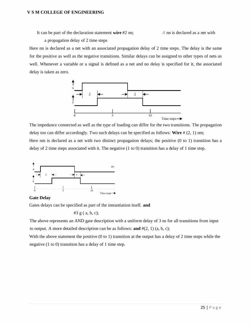
It can be part of the declaration statement wire #2 nn; // nn is declared as a net with
a propagation delay of 2 time steps
Here nn is declared as a net with an associated propagation delay of 2 time steps. The delay is the same
for the positive as well as the negative transitions. Similar delays can be assigned to other types of nets as
well. Whenever a variable or a signal is defined as a net and no delay is specified for it, the associated
delay is taken as zero.
The impedance connected as well as the type of loading can differ for the two transitions. The propagation
delay too can differ accordingly. Two such delays can be specified as follows: Wire # (2, 1) nm;
Here nm is declared as a net with two distinct propagation delays; the positive (0 to 1) transition has a
delay of 2 time steps associated with it. The negative (1 to 0) transition has a delay of 1 time step.
Gate Delay
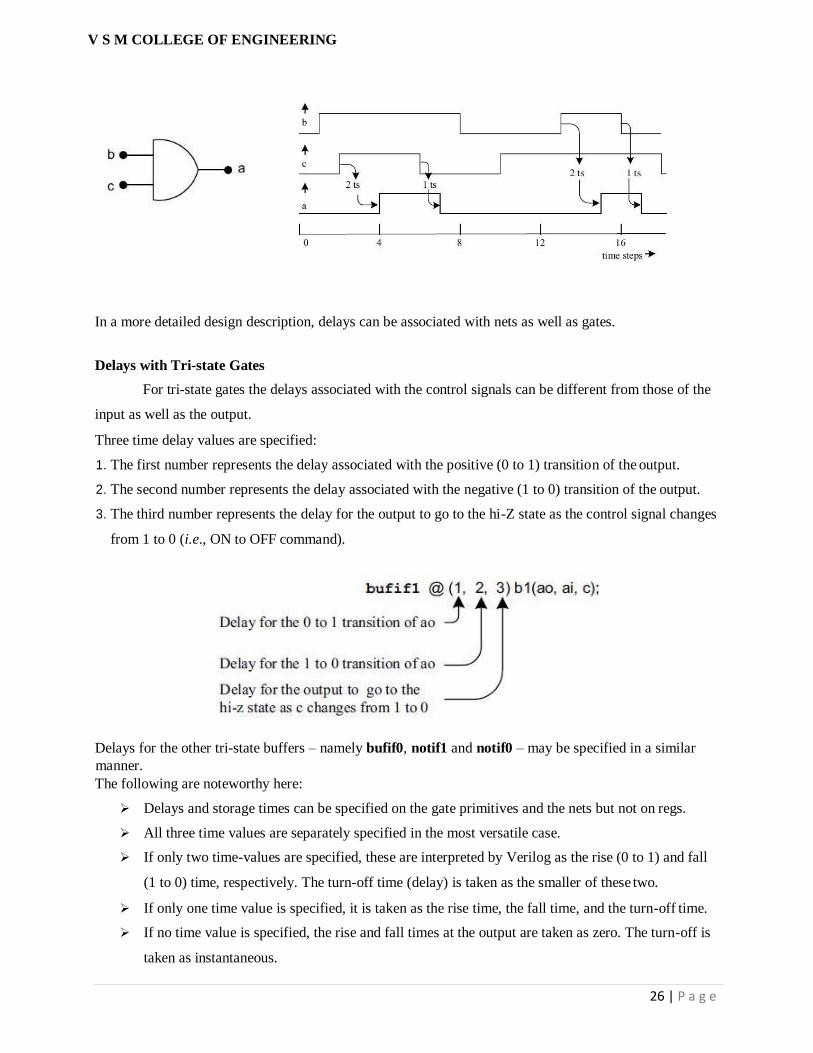
Gates delays can be specified as part of the instantiation itself. and
#3 g ( a, b, c);
The above represents an AND gate description with a uniform delay of 3 ns for all transitions from input
to output. A more detailed description can be as follows: and #(2, 1) (a, b, c);
With the above statement the positive (0 to 1) transition at the output has a delay of 2 time steps while the
negative (1 to 0) transition has a delay of 1 time step.
26 | P a g e
V S M COLLEGE OF ENGINEERING
In a more detailed design description, delays can be associated with nets as well as gates.
Delays with Tri-state Gates
For tri-state gates the delays associated with the control signals can be different from those of the
input as well as the output.
Three time delay values are specified:
1. The first number represents the delay associated with the positive (0 to 1) transition of the output.
2. The second number represents the delay associated with the negative (1 to 0) transition of the output.
3. The third number represents the delay for the output to go to the hi-Z state as the control signal changes
from 1 to 0 (i.e., ON to OFF command).
Delays for the other tri-state buffers – namely bufif0, notif1 and notif0 – may be specified in a similar
manner.
The following are noteworthy here:
Delays and storage times can be specified on the gate primitives and the nets but not on regs.
All three time values are separately specified in the most versatile case.
If only two time-values are specified, these are interpreted by Verilog as the rise (0 to 1) and fall
(1 to 0) time, respectively. The turn-off time (delay) is taken as the smaller of these two.
If only one time value is specified, it is taken as the rise time, the fall time, and the turn-off time.
If no time value is specified, the rise and fall times at the output are taken as zero. The turn-off is
taken as instantaneous.
27 | P a g e
V S M COLLEGE OF ENGINEERING
It is customary for manufacturers to specify delays and their range in the following manner:
Max delay: The maximum value of the delay in a batch; that is, the delay encountered in practice
is guaranteed to be less than this in the worst case.
Min. delay: Minimum value of delay in a batch; that is, the specified signal is guaranteed to be
available only after a minimum of time specified.
Typ. delay: Typical or representative value of the delay.
Each of the delays in a gate primitive or for a net can be specified in terms of these three values.
For example and #(2:3:4) g1(a0, a1, a2);
can instantiate an AND gate with the following time delay specifications:
The 0 to 1 rise time and the 1 to 0 fall time are equal.
The minimum value of either is 2 time steps. Typical value is 3 time steps and the maximum
value is 4 time steps.
Note that the colon that separates the numbers signifies that the timings specified are the
minimum, typical, and maximum values.
If the same is not specified, the simulation is carried out with the typical delay value.
The group of minimum, typical, and maximum delay values for the propagation delays can be specified
separately for any gate primitive. Thus an AND gate primitive can be specified as and #(1:2:3, 2:4:6)
g2(b0, b1, b2);
Here for the 0 to 1 transition of the output (rise time) the gate has a minimum delay value of 1 ns, a
typical value of 2 ns, and a maximum value of 3 ns. Similarly, for the 1 to 0 transition (fall time) the gate
has a minimum delay value of 2 ns, a typical delay value of 4 ns, and a maximum delay value of 6 ns.
Such delay specifications can be associated with nets as well as tri-state type gates also.
wire #(1:2:3) a; /* The net a has a propagation delay whose minimum,
typical and maximum values are 1 ns, 2 ns, and 3 ns,
respectively*/
bufif1 #(1:2:3, 2:4:6, 3:6:9) g3 (a0, b0, c0);
The different delay values for the buffer are as follows:
The output rise time (0 to 1 transition) has a minimum value of 1 ns, a typical value of 2 ns and a
maximum value of 3 ns.
The output fall time (1 to 0 transition) has a minimum value of 2 ns, a typical value of 4 ns and a
maximum value of 6 ns.
The output turn-off time (1 to 0) has a minimum value of 3 ns, a typical value of 6 ns, and a
maximum value of 9 ns
28 | P a g e
V S M COLLEGE OF ENGINEERING
The following general observations are in order regarding the overall delays through the circuit:
A normal design can have many gates and nets in its signal paths. The delay through any path for
a signal depends on the path and the type of transitions at each stage.
The cumulative delay for a signal in a path puts an upper limit on the maximum operating
frequency vis-à-vis the signal.
A signal may go through multiple paths in a design to arrive at one gate. It is necessary to match
the delays within specified tolerances for reliable operation of the device.
In larger designs, one has to identify the longest signal path (critical path).
This puts an upper limit on the operating frequency apart from causing maloperation in a
worstcase scenario. One of the practices in design is to reroute selected signals or redo selected
design segments to reduce critical path delays.
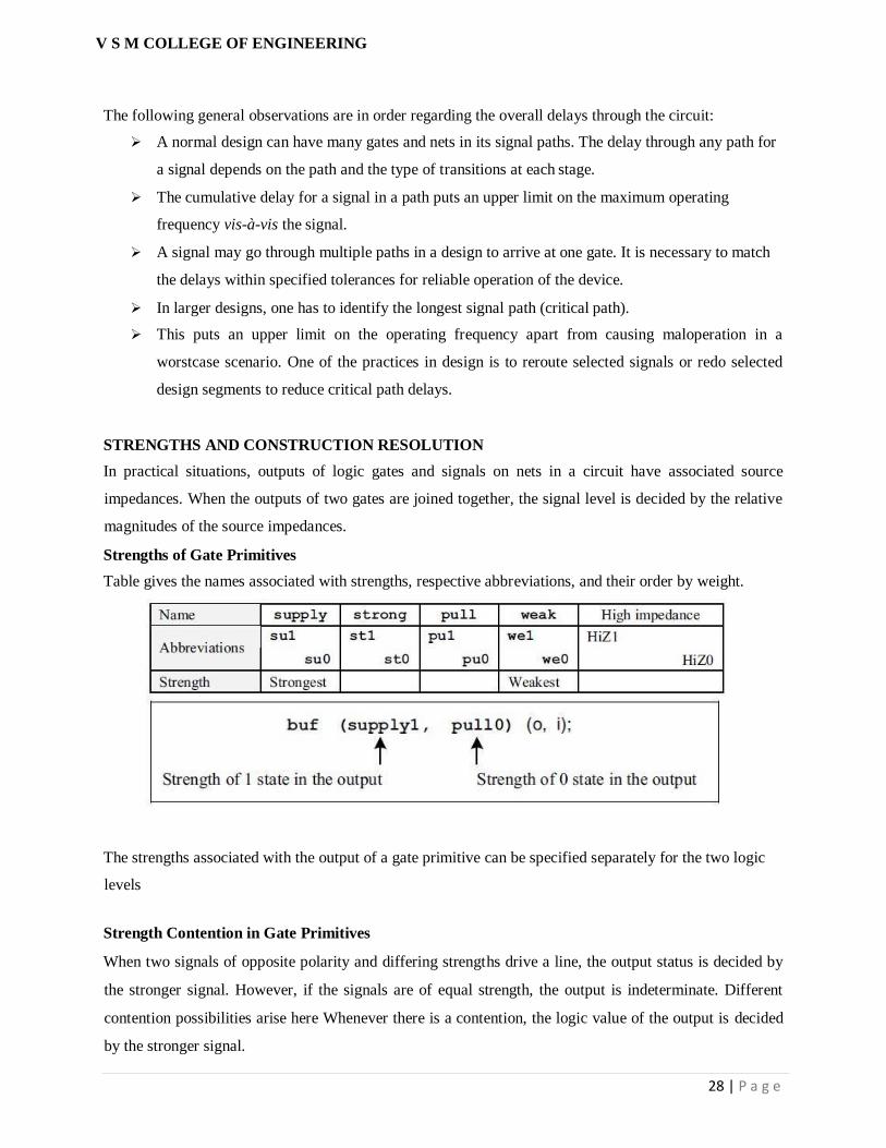
STRENGTHS AND CONSTRUCTION RESOLUTION
In practical situations, outputs of logic gates and signals on nets in a circuit have associated source
impedances. When the outputs of two gates are joined together, the signal level is decided by the relative
magnitudes of the source impedances.
Strengths of Gate Primitives
Table gives the names associated with strengths, respective abbreviations, and their order by weight.
The strengths associated with the output of a gate primitive can be specified separately for the two logic
levels
Strength Contention in Gate Primitives
When two signals of opposite polarity and differing strengths drive a line, the output status is decided by
the stronger signal. However, if the signals are of equal strength, the output is indeterminate. Different
contention possibilities arise here Whenever there is a contention, the logic value of the output is decided
by the stronger signal.
29 | P a g e
V S M COLLEGE OF ENGINEERING
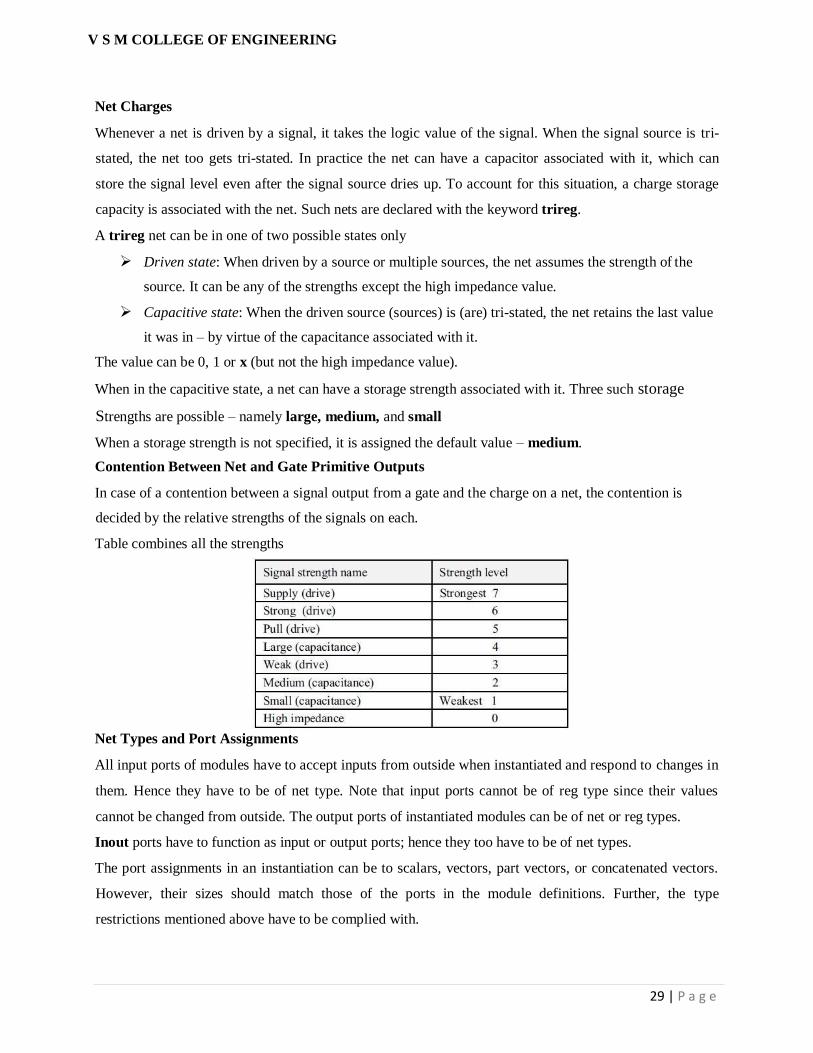
Net Charges
Whenever a net is driven by a signal, it takes the logic value of the signal. When the signal source is tri-
stated, the net too gets tri-stated. In practice the net can have a capacitor associated with it, which can
store the signal level even after the signal source dries up. To account for this situation, a charge storage
capacity is associated with the net. Such nets are declared with the keyword trireg.
A trireg net can be in one of two possible states only
Driven state: When driven by a source or multiple sources, the net assumes the strength of the
source. It can be any of the strengths except the high impedance value.
Capacitive state: When the driven source (sources) is (are) tri-stated, the net retains the last value
it was in – by virtue of the capacitance associated with it.
The value can be 0, 1 or x (but not the high impedance value).
When in the capacitive state, a net can have a storage strength associated with it. Three such storage
Strengths are possible – namely large, medium, and small
When a storage strength is not specified, it is assigned the default value – medium.
Contention Between Net and Gate Primitive Outputs
In case of a contention between a signal output from a gate and the charge on a net, the contention is
decided by the relative strengths of the signals on each.
Table combines all the strengths
Net Types and Port Assignments
All input ports of modules have to accept inputs from outside when instantiated and respond to changes in
them. Hence they have to be of net type. Note that input ports cannot be of reg type since their values
cannot be changed from outside. The output ports of instantiated modules can be of net or reg types.
Inout ports have to function as input or output ports; hence they too have to be of net types.
The port assignments in an instantiation can be to scalars, vectors, part vectors, or concatenated vectors.
However, their sizes should match those of the ports in the module definitions. Further, the type
restrictions mentioned above have to be complied with.
30 | P a g e
V S M COLLEGE OF ENGINEERING
NET TYPES
wire is possibly the simplest type of net declaration.
wand and wor Types of Nets
DESIGN OF BASIC CIRCUITS
Example ALU
The ALU considered carries out four functions:
Addition of two 4-bit numbers.
Complementing all the bits of a 4-bit vector.
Bit-by-bit AND operation on two nibbles.
Bit-by-bit XOR operation on two nibbles.
module add4g(sum,carry,a,b,cin);
input[3:0]a,b; input cin; output[3:0]sum;
output carry; wire [2:0]cc; fa
a0(sum[0],cc[0],a[0],b[0],cin); fa
a1(sum[1],cc[1],a[1],b[1],cc[0]); fa
a2(sum[2],cc[2],a[2],b[2],cc[1]); fa
a3(sum[3],carry,a[3],b[3],cc[2]);
endmodule
module andg4(c,a,b);
input[3:0]a,b;
output[3:0]c;
and(c[0],a[0],b[0]);
and(c[1],a[1],b[1]);
and(c[2],a[2],b[2]);
and(c[3],a[3],b[3]);
endmodule
module xorg(c,a,b); input[3:0]a,b;
output[3:0]c; wire [3:0]cc;
xor x0(c[0],a[0],b[0]); xor
x1(c[1],a[1],b[1]); xor
31 | P a g e
V S M COLLEGE OF ENGINEERING
x2(c[2],a[2],b[2]); xor
x3(c[3],a[3],b[3]);
endmodule
module compl(c,a);
input[3:0]a;
output[3:0]c;
not(c[0],a[0]);
not(c[1],a[1]);
not(c[2],a[2]);
not(c[3],a[3]);
endmodule
2-to-4 decoder
module dec2_4 (a,b,en);
output [3:0] a; input [1:0]b; input en; wire [1:0]bb; not(bb[1],b[1]),(bb[0],b[0]);
and(a[0],en,bb[1],bb[0]), (a[1],en,bb[1],b[0]), (a[2],en,b[1],bb[0]), (a[3],en,b[1],b[0]);
endmodule
4-to-1 mux module
module mux4_1alu(y,i,e); input
[3:0] i; input e; output [3:0]y; bufif1
g1(y[3],i[3],e); bufif1
g2(y[2],i[2],e); bufif1
g3(y[1],i[1],e); bufif1
g4(y[0],i[0],e);
endmodule
module alu_4g(a,b,c,carry,cin,cen,s); input
[3:0]a,b; input[1:0]s; input cen,cin;
output [3:0]c; output carry; wire [3:0]
data0,data1,data2,data3,e; wire carry1 ;
dec2_4 m5(e,s,cen); add4g
m1(data0,carry1,a,b,cin); compl
m2(data1,a); xorg m3(data2,a,b); andg4
m4(data3,a,b); bufif1
32 | P a g e
V S M COLLEGE OF ENGINEERING
g5(carry,carry1,cen); mux4_1alu
m6(c,data0,e[0]); mux4_1alu
m7(c,data1,e[1]); mux4_1alu
m8(c,data2,e[2]); mux4_1alu
m9(c,data3,e[3]);
endmodule
MODELING AT DATA FLOW LEVEL
CONTINUOUS ASSIGNMENT STRUCTURES
A simple two input AND gate in data flow format has the form assign c = a && b; Here � ―assign‖ is the keyword carrying out the assignment operation. This type of assignment is called a
continuous assignment.
� a and b are operands – typically single-bit logic variables. � ―&&‖ is a logic operator. It does the bit-wise AND operation on the two operands a and b.
� ―=‖ is an assignment activity carried out.
� c is a net representing the signal which is the result of the assignment.
In general, an operand can be of any one of the following types:
� A constant number [including real].
� Net of a scalar or vector type including part of a vector.
� Register variable of a scalar or vector type including part of a vector. � Memory element.
� A call to a function that returns any of the above. The function itself can be a user-defined or of a
system type
DELAYS AND CONTINUOUS ASSIGNMENTS
Delays can be incorporated at the data flow level in different ways. Consider the combination of statements. The assignment takes effect with a time delay of 2 time steps. If a or b changes in value, the
program waits for 2 time steps, computes the value of c based on the values of a and b at the time of
computation, and assigns it to c. In the interim period, a or b may change further, but c changes and takes the new value only 2 time steps after the change in a or b initiates it. Typical waveforms for a, b, and c are
shown. Note that the changes in a and b of duration less than 2 time steps are ignored vis-à-vis assignment
to the net c. The following may be noted with respect to the waveforms:
� a changes at 0 ns, 2 ns, 5 ns, 8 ns, 9 ns, 12 ns and 13 ns; b changes at 0 ns, 2 ns, 6 ns, 8 ns and 13 ns. All
these trigger changes to c.
� In every case change to c comes into effect with a time delay of 2 time steps – that is, at the 2nd, 4th,
7th, 8th, 10th, 11th, 14th and 15th ns, respectively.
� Whenever c changes, its new value is decided by the values of a and b at that instant of time. In effect, c
changes at 2nd, 4th and 7th ns only.
ASSIGNMENT TO VECTORS
The continuous assignments are equally applicable to vectors. A single statement can describe operations
involving vectors wherever possible. This is illustrated in the adder module, which adds two 8-bit numbers. Here it is assumed that the sum is also of 8 bits. However to account for the possibility of a carry
bit being generated in the course of the addition process, it is desirable to increase the vector size of c by
one bit.
33 | P a g e
V S M COLLEGE OF ENGINEERING
Concatenation of Vectors
One can concatenate vectors, scalars, and part vectors to form other vectors. The concatenated vector is
enclosed within braces. Commas separate the components –scalars, vectors, and part vectors. If a and b are 8- and 4-bit wide vectors, respectively and c is a scalar {a, b, c} stands for a concatenated vector of 13 bits
width. The vector components are formed in the order shown – c is the least significant bit and a[7] the
most significant bit and the other bits are in between in the order specified. The concatenation can be with selected segments of vectors also. For example, {a(7:4), b(2:0)} represents a 7-bit vector formed by
combining the 4 most significant bits of vector a with the 3 least significant bits of vector b. The size of
each operand within the braces has to be specified fully to form the concatenated vector.
OPERATORS
A set of operators is available in Verilog. The operator symbols are similar to those in C language [Gottfried]. With these operators we can carry out specified operations on the operands and assign the
results to a net or a vector set of nets as the case may be. A few such operands have already been used in
the examples so far. We discuss here the different operators, their types, and the operations carried out by each. Subsequently the use of operators is illustrated through a set of examples.
Unary Operators
Unary operators do an operation on a single operand and assign the result to the specified net. The unary
operators in Verilog are given in Table 6.1. All unary operators get precedence over binary and ternary operators. The operators ―+‖ and ―–― preceding an integer or a real number change its sign. These are also
unary operators
Binary Operators
Most operators available are of the binary type. A binary operator takes on two operands; the operator
comes in between the two operands in the assignment. The binary operators are grouped into type categories and discussed separately. The following are to be noted:
� The arithmetic operators treat both the operands as numbers and return the result as a number. � All net and reg operand values are treated as unsigned numbers.
� Real and integer operands may be signed quantities. � If either of the operand values has a zero value, the entire result has a zero value (?). The result of any arithmetic operation — with the ―+‖ or ―–‖ or with any of the other arithmetic operators
discussed later — will have an x value if any of the operand bits has an x or a z value.
34 | P a g e
V S M COLLEGE OF ENGINEERING
BEHAVIORAL MODELING
UNIT - III
Introduction, Operations and Assignments, Functional Bifurcation, Initial Construct, Always Construct,
Examples, Assignments with Delays, Wait construct, Multiple Always Blocks, Blocking and Non blocking Assignments, The case statement, iƒ and iƒ-else constructs, Assign-de-assign construct, repeat
construct, for loop , The disable construct, while loop, forever loop, Parallel blocks, Force-release,
construct, Event --------------------------------------------------------------------------------------------------------------------------------
INTRODUCTION
Behavioral level modeling constitutes design description at an abstract level. One can visualize
the circuit in terms of its key modular functions and their behavior; it can be described at a functional
level itself instead of getting bogged down with implementation details.
OPERATIONS AND ASSIGNMENTS
The design description at the behavioral level is done through a sequence of assignments. These are called
‗procedural assignments‘
The procedure assignment is characterized by the following:
The assignment is done through the ―=‖ symbol (or the ―<=‖ symbol) as was the case with the
continuous assignment earlier.
An operation is carried out and the result assigned through the ―=‖ operator to an operand
specified on the left side of the ―=‖ sign – for example, N = ~N; Here the content of reg N is
complemented and assigned to the reg N itself. The assignment is essentially an updating activity.
The operation on the right can involve operands and operators. The operands can be of different
types – logical variables, numbers – real or integer and so on.
All the operands are given in Tables 6.1 to 6.9. The format of using them and the rules of
precedence remain the same.
The operands on the right side can be of the net or variable type. They can be scalars or vectors.
It is necessary to maintain consistency of the operands in the operation expression –
e.g., N = m / l; Here m and l have to be same types of quantities – specifically a reg,
integer, time, real, realtime, or memory type of data – declared in advance.
The operand to the left of the ―=‖ operator has to be of the variable (e.g., reg) type. It has to be
specifically declared accordingly. It can be a scalar, a vector, a part vector, or a concatenated
vector.
Procedural assignments are very much like sequential statements in C. Normally they are carried
out one at a time sequentially. As soon as a specified operation on the right is carried out, the
result is assigned to the quantity on the left – for example N = m + l; N1 = N * N;The above
35 | P a g e
V S M COLLEGE OF ENGINEERING
form a set of two procedures placed within an always block. Generally they are carried out
sequentially in the order specified
The sequential nature of the assignments requires the operands on the left of the assignment to be of reg
(variable) type.
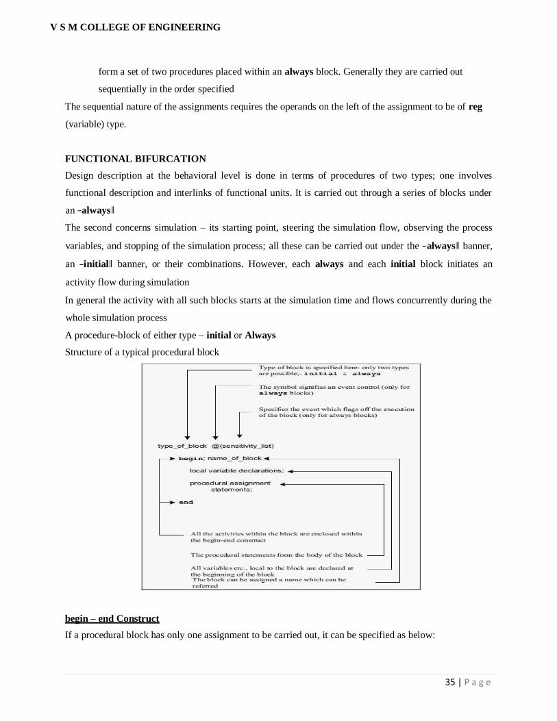
FUNCTIONAL BIFURCATION
Design description at the behavioral level is done in terms of procedures of two types; one involves
functional description and interlinks of functional units. It is carried out through a series of blocks under
an ―always‖
The second concerns simulation – its starting point, steering the simulation flow, observing the process
variables, and stopping of the simulation process; all these can be carried out under the ―always‖ banner,
an ―initial‖ banner, or their combinations. However, each always and each initial block initiates an
activity flow during simulation
In general the activity with all such blocks starts at the simulation time and flows concurrently during the
whole simulation process
A procedure-block of either type – initial or Always
Structure of a typical procedural block
begin – end Construct
If a procedural block has only one assignment to be carried out, it can be specified as below:
36 | P a g e
V S M COLLEGE OF ENGINEERING
initial #2 a=0;
If more than one procedural assignment is to be carried out in an initial block. All such assignments are
grouped together between ―begin‖ and ―end‖ declarations.
The following are to be noted here:
Every begin declaration must have its associated end declaration.
begin – end constructs can be nested as many times as desired.
Name of the Block
Any block can be assigned a name, but it is not mandatory. Only the blocks which are to be identified and
referred by the simulator need be named.
Assigning names to blocks serves different purposes:
Registers declared within a block are local to it and are not available outside. However, during
simulation they can be accessed for simulation, etc., by proper dereferencing. Named blocks
can be disabled selectively when desired
Local Variables
Variables used exclusively within a block can be declared within it. Such a variable need not be
declared outside, in the module encompassing the block. Such local declarations conserve memory and
offer other benefits too. Regs declared and used within a block are static by nature. They retain their
values at the time of leaving the block. The values are modified only at the next entry to the block.
INITIAL CONSTRUCT
A set of procedural assignments within an initial construct are executed only once – and, that too,
at the times specified for the respective assignments The initial process is characterized by the following
In any assignment statement the left-hand side has to be a storage type of element (and not a net).
It can be a reg, integer, or real type of variable. The right-hand side can be a storage type of
variable (reg, integer, or real type of variable) or a net.
All the procedural assignments appear within a begin–end block
All the procedural assignments are executed sequentially – in the same order as they appear in the
design description.
The initial block above does three controlling activities during the simulation run.
Initialize the selected set of reg's at the start.
Change values of reg's at predetermined instances of time. These form the inputs to the module(s)
under test and test it for a desired test sequence.
Stop simulation at the specified time.

37 | P a g e
V S M COLLEGE OF ENGINEERING
Multiple Initial Blocks
A module can have as many initial blocks as desired. All of them are activated at the start of simulation.
The time delays specified in one initial block are exclusive of those in any other block.
ALWAYS CONSTRUCT
The always process signifies activities to be executed on an ―always basis.‖ Its
essential characteristics are:
Any behavioral level design description is done using an always block.
The process has to be flagged off by an event or a change in a net or a reg.
The process can have one assignment statement or multiple assignment statements. In the latter
case all the assignments are grouped together within a ―begin – end‖ construct.
Normally the statements are executed sequentially in the order they appear.
Event Control
The always block is executed repeatedly and endlessly. It is necessary to specify a condition or a set of
conditions, which will steer the system to the execution of the block. Alternately such a flagging-off can
be done by specifying an event preceded by the symbol ―@”.
@(negedge clk) : executes the following block at the negative edge of the reg (variable) clk.
@(posedge clk) : executes the following block at the positive edge of the reg (variable) clk.
@clk : executes the following block at both the edges of clk.
The events can be changes in reg, integer, real or a signal on a net. These should be declared
beforehand.
No algebra or logic operation is permitted as an event. The OR'ing signifies ―execute the block if
any one of the events takes place.‖
The positive transition for a reg type single bit variable is a change from 0 to1.
For a logic variable it is a transition from false to true.
The ―posedge‖ transition for a signal on a net can be of three different types:
0 to1
0 to x or z
x or z to 1
The ―negedge‖ transition for a signal on a net can be of three different types:-
38 | P a g e
V S M COLLEGE OF ENGINEERING
1 to 0
1 to x or z
x or z to 0
If the event specified is in terms of a multibit reg, only its least significant bit is considered for the
transition. Changes in the other bits are ignored. The event-based flagging-off of a block is applicable
only to the always block.
According to the recent version of the LRM, the comma operator (,) plays the same role as the keyword
or. The two can be used interchangeably or in a mixed form. Thus the following are identical: @ (a or b
or c)
@ (a or b, c)
@ (a, b, c)
@ (a, b or c)
EXAMPLES
Versatile Counter module
counterup(a,clk,N);
input clk;
input[3:0]N;
output[3:0]a;
reg[3:0]a;
initial a=4'b0000;
always@(negedge clk) a=(a==N)?4'b0000:a+1'b1;
endmodule
TEST_BENCH
module tst_counterup;
reg clk;
reg[3:0]N;
wire[3:0]a;
counterup c1(a,clk,N);
39 | P a g e
V S M COLLEGE OF ENGINEERING
initial
begin
end
clk = 0;
N = 4'b1011;
always #2 clk=~clk;
initial $monitor($time,"a=%b,clk=%b,N=%b",a,clk,N);
endmodule
module counterdn(a,clk,N);
input clk;
input[3:0]N;
output[3:0]a;
reg[3:0]a;
initial a =4'b0000;
always@(negedge clk) a=(a==4'b0000)?N:a-1'b1;
endmodule
module updcounter(a,clk,N,u_d);
input clk,u_d;
input[3:0]N;
output[3:0]a;
reg[3:0]a;
initial a =4'b0000;
always@(negedge clk) a = (u_d) ? ( (a==N) ? 4'b0000 : a + 1'b1) : (
(a==4'b0000) ? N : a - 1'b1);
endmodule
40 | P a g e
V S M COLLEGE OF ENGINEERING
module clrupdcou(a,clr,clk,N,u_d);
input clr,clk,u_d;
input[3:0]N;
output[3:0]a;
reg[3:0]a;
initial a =4'b0000;
always@(negedge clk or posedge clr) a = (clr) ? 4'h0 : ( (u_d) ? ( (a==N) ? 4'b0000 : a+1'b1) :(
(a == 4'b0000) ? N : a - 1'b1));
endmodule
Example Shift Register
module shifrlter(a,clk,r_l);
input clk,r_l;
output [7:0]a;
reg[7:0]a;
initial a= 8'h01;
always@(negedge clk) begin a = (r_l) ?
(a>>1'b1) : (a<<1'b1);
end
endmodule
Example 3 Clocked Flip-Flop
module dff(do,di,clk); output
do; input di,clk; reg do;
initial
do=1'b0;
41 | P a g e
V S M COLLEGE OF ENGINEERING
always @ (negedge clk) do = di;
endmodule
Example 4 D Latch
module
dffen(do,di,en);
output do; input di,en;
reg do;
initial
do=1'b0;
always@(di or en)
if(en) do=di;
endmodule
Example 5 Clock Waveform
Consider the design description line always
#3 clk = ~clk;
The sequence of operation taking place within this line segment is as follows:
When the system comes across the statement, it schedules an activity 3 ns later.
At the end of the 3 ns, the value of clk is sensed; the sensed value is complemented and then stored
temporarily.
Then the stored value is assigned to the clock, which completes the activity of the always block; once
again, execution resumes at step 1.
ASSIGNMENTS WITH DELAYS
The delay refers to the specific activity it qualifies. A variety of possibilities of specifying delays to
assignments exist. Consider the assignment always #3 b = a;
Simulator encounters this at zero time and posts the entire activity to be done 3 ns later the assignment is
scheduled to be repeated every 3 ns, irrespective of whether a changes in the Meantime
Intra-assignment Delays
In contrast, the ―intra-assignment‖ delay carries out the assignment in two parts
42 | P a g e
V S M COLLEGE OF ENGINEERING
A = # dl expression;
Here the expression is scheduled to be evaluated as soon as it is encountered. However, the result of the
evaluation is assigned to the right-hand side quantity a after a delay specified by dl. dl can be an integer or
a constant expression
Zero Delay
A delay of 0 ns does not really cause any delay. However, it ensures that the assignment following is
executed last in the concerned time slot. Often it is used to avoid indecision in the precedence of
execution of assignments
wait CONSTRUCT
The wait construct makes the simulator wait for the specified expression to be true before proceeding
with the following assignment or group of assignments. Its syntax has the form wait (alpha) assignment1;
alpha can be a variable, the value on a net, or an expression involving them. If alpha is an expression, it is
evaluated; if true, assignment1 is carried out. One can also have a group of assignments within a block in
place of assignment1. The activity is level-sensitive in nature, in contrast to the edge-sensitive nature of
event specified through @.
Specifically the procedural assignment
@clk a = b; assigns the value of b to a when clk changes; if the value of b changes when clk is steady, the
value of a remains unaltered.
wait(clk) #2 a = b; the simulator waits for the clock to be high and then assigns b to a with a delay of 2 ns.
The assignment will be refreshed as long as the clk remains high
DESIGNS AT BEHAVIORAL LEVEL
module aoibeh(o,a,b); output o; input[1:0]a,b;
reg o,a1,b1,o1; always@(a[1] or a[0]or
b[1]or b[0]) begin a1=&a; b1=&b;
o1=a1||b1; o=~o1;
end
endmodule
module aoibeh1(o,a,b); output o;
input[1:0]a,b; reg o;
always@(a[1]ora[0]or b[1]orb[0])
o=~((&a)||(&b));
43 | P a g e
V S M COLLEGE OF ENGINEERING
endmodule
BLOCKING AND NONBLOCKING ASSIGNMENTS
These are executed sequentially – that is, one statement is executed, and only then the following
one is executed. Such assignments block the execution of the following lot of assignments at any time
step. Hence they are called ―blocking assignments‖.
A facility called the ―nonblocking assignment‖ is available for such situations. The symbol ―<=‖
signifies a non-blocking assignment. The same symbol signifies the ―less than or equal to‖ operator in the
context of an operation. The context decides the role of the symbol. The main characteristic of a
nonblocking assignment is that its execution is concurrent with that of the following assignment or
activity.
Nonblocking Assignments and Delays
Delays – of the assignment type and the intra-assignment type – can be associated with nonblocking
assignments also. The principle of their operation is similar to that with blocking assignments.
THE case STATEMENT
The case statement is an elegant and simple construct for multiple branching in a module. The keywords
case, endcase, and default are associated with thecase construct.
Format of the case construct is
Case (expression)
Ref1 : statement1;
Ref2 : statement2;
Ref3 : statement3;
.. .
. . .
default: statementd;
endcase
If the evaluated value matches ref1, statement1 is executed; and the simulator exits the block; Else
expression is compared with ref2 and in case of a match, statement2 is executed, and so on. If none of the
ref1, ref2, etc., matches the value of expression, the default statement is executed. A statement or a group
of statements is executed if and only if there is an exact – bit by bit – match between the evaluated
expression and the specified ref1, ref2, etc.
44 | P a g e
V S M COLLEGE OF ENGINEERING
For any of the matches, one can have a block of statements defined for execution. The block
should appear within the begin-end construct.
There can be only one default statement or default block. It can appearanywhere in the case
statement.
One can have multiple signal combination values specified for the same statement for execution.
Commas separate all of them.
module dec2_4beh(o,i);
output[3:0]o;
input[1:0]i;
reg[3:0]o;
always@(i) begin
case(i)
2'b00:o=4'h0;
2'b01:o=4'h1;
2'b10:o=4'h2;
2'b11:o=4'h4;
default: begin
$display ("error"); o=4'h0;
endcase
end endmodule
end
module dec2_4beh1(o,i);
output[3:0]o; input[1:0]i;
reg[3:0]o; always@(i)
begin case(i)
2'b00:o[0]=1'b1;
2'b01:o[1]=1'b1;
2'b10:o[2]=1'b1;
2'b11:o[3]=1'b1;
2'b0x,2'b1x,2'bx0,2'bx1:o=4'b0000; default:
begin
endcase
end
$display ("error"); o=4'h0;
45 | P a g e
V S M COLLEGE OF ENGINEERING
end endmodule
module alubeh(c,s,a,b,f);
output[3:0]c; output s;
input [3:0]a,b;
input[1:0]f; reg s;
reg[3:0]c; always@(a
or b or f)
begin case(f)
2'b00: c=a+b;
2'b01: c=a-b;
2'b10: c=a&b;
2'b11: c=a|b;
Endcase end
endmodule
Casex and Casez
The case statement executes a multiway branching where every bit of the case expression contributes to
the branching decision. The statement has two variants where some of the bits of the case expression can
be selectively treated as don‘t cares – that is, ignored. Casez allows z to be treated as a don‘t care. ―?‖
character also can be used in place of z. casex treats x or z as a don‘t care
module pri_enc(a,b);
output[1:0]a;
input[3:0]b; reg[1:0]a;
always@(b) casez(b)
4'bzzz1:a=2'b00;
4'bzz10:a=2'b01;
4'bz100:a=2'b10;
4'b1000:a=2'b11; endcase
endmodule
SIMULATION FLOW
Verilog has to be an inherently parallel processing language. The fact that all the elements of a digital
circuit (or any electronic circuit for that matter) function and interact continuously conforming to their
46 | P a g e
V S M COLLEGE OF ENGINEERING
interconnections demands parallel processing. In Verilog theparallel processing is structured through the
following [IEEE]:
Simulation time: Simulation is carried out in simulation time.
The simulator functions with simulation time advancing in (equal) discrete steps.
At every simulation step a number of active events are sequentially carriedout.
The simulator maintains an event queue – called the ―Stratified Event Queue‖ with an active
segment at its top. The top most event in the active segment of the queue is taken up for execution
next.
The active event can be of an update type or evaluation type. The evaluation event can be for
evaluation of variables, values on nets, expressions, etc. Refreshing the queue and rearranging it
constitutes the update event.
Any updating can call for a subsequent evaluation and vice versa.
Only after all the active events in a time step are executed, the simulation advances to the next
time step.
Completion of the sequence of operations above at any time step signifies the parallel nature of the HDL.
A number of active events can be present for execution at any simulation time step; all may vie for
―attention.‖ Amongst these, an event specified at #0 time is scheduled for execution at the end
Stratified Event Queue
The events being carried out at any instant give rise to other events – inherent in the execution process.
All such events can be grouped into the following 5 types:
Active events – explained above.
Inactive events – The inactive events are the events lined up for execution immediately after the
execution of the active events. Events specified with zero delay are all inactive events.
Blocking Assignment Events – Operations and processes carried out at previous time steps with
results to be updated at the current time step are of this category.
Monitor Events – The Monitor events at the current time step – $monitor and $strobe – are to be
processed after the processing of the active events, inactive events, and nonblocking assignment
events.
Future events – Events scheduled to occur at some future simulation time are the future events.
The simulation process conforming to the stratified event queue is shown in flowchart form in Figure
47 | P a g e
V S M COLLEGE OF ENGINEERING
if AND if-else CONSTRUCTS
The if construct checks a specific condition and decides execution based on the result. the structure of a
segment of a module with an if statement. After execution of assignment1, the condition specified is
checked. If it is satisfied, assignment2 is executed; if not, it is skipped. In either case the execution
continues through assignment3, assignment4, etc. Execution of assignment2 alone is dependent on the
condition. The rest of the sequence remains.
. . .
assignment1; if (condition)
assignment2; assignment3;
assignment4;
. . .
48 | P a g e
V S M COLLEGE OF ENGINEERING
Use of the if–else construct
. . .
assignment1;
if(condition) begin //
Alternative 1
assignment2;
assignment3; end else
begin //alternative 2
assignment4;
assignment5; end
assignment6;
. . . .
. .
After the execution of assignment1, if the condition is satisfied, alternative1 is followed and assignment2
and assignment3 are executed. Assignment4 and assignment 5 are skipped and execution proceeds with
assignment6.
If the condition is not satisfied, assignment2 and assignment3 are skipped and assignment4 and
assignment5 are executed. Then execution continues with assignment6.
module demux(a,b,s); output [3:0]a; input b;
input[1:0]s; reg[3:0]a; always@(b or s)
begin if(s==2'b00) begin a[2'b0]=b;
a[3:1]=3'bZZZ;
endmodule
end
end else
if(s==2'b01) begin
a[2'd1]=b;
{a[3],a[2],a[0]}=3'bZZZ;
end else if(s==2'b10) begin
a[2'd2]=b;
{a[3],a[1],a[0]}=3'bZZZ;
end else begin a[2'd3]=b;
a[2:0]=3'bZZZ;
end
49 | P a g e
V S M COLLEGE OF ENGINEERING
//counter using if else if; module
countif(a,clk); output[7:0]a; input
clk; reg[7:0]a,n; initial begin
n=8'h0a; a=8'b00000000;
#45 n=8'h23;
end always@(posedge
clk) begin
$write ("time=%0d ",$time);
if(a==n) a=8'h00; else
a=a+1'b1;
end endmodule
assign–deassign CONSTRUCT
The assign – deassign constructs allow continuous assignments within a behavioral block.
always@(posedge clk) a = b;
By way of execution, at the positive edge of clk the value of b is assigned to variable a, and a remains
frozen at that value until the next positive edge of clk. Changes in b in the interval are ignored.
Consider the block always@(posedge clk)
assign c = d;
Here at the positive edge of clk, c is assigned the value of d in a continuous manner; subsequent changes
in d are directly reflected as changes in variable c: The assignment here is akin to a direct (one way )
electrical connection to c from d established at the positive edge of clk.
Consider an enhanced version of the above block as
Always Begin
@(posedge
clk) assign c =
d; @(negedge
clk) deassign
c; end
The above block signifies two activities:
1. At the positive edge of clk, c is assigned the value of d in a continuous manner
2. At the following negative edge of clk, the continuous assignment to c is removed; subsequent changes
to d are not passed on to c; it is as though c is electrically disconnected from d.
50 | P a g e
V S M COLLEGE OF ENGINEERING
In short, assign allows a variable or a net change in the sensitivity list to mandate a subsequent
continuous assignment within. deassign terminates the assignment done through the assign-based
statement.
module demux1(a0,a1,a2,a3,b,s); output
a0,a1,a2,a3; input b; input [1:0]s; reg a0,a1,a2,a3;
always@(s) if(s==2'b00) assign
{a0,a1,a2,a3}={b,3'oz};
else if(s==2'b01) assign
{a0,a1,a2,a3}={1'bz,b,2'bz};
else if(s==2'b10) assign
{a0,a1,a2,a3}={2'bz,b,1'bz};
else if(s==2'b11)
assign {a0,a1,a2,a3}={3'oz,b};
endmodule
D Flip-Flop through assign – deassign Constructs module
dffassign(q,qb,di,clk,clr,pr); output q,qb; input di,clk,clr,pr; reg q; assign
qb=~q; always@(clr or pr) begin if(clr)assign q = 1'b0;//asynchronous
clear and if(pr) assign q = 1'b1;// preset of FF overrides else deassign q;//
the synchronous behaviour
end always@(posedge clk) q = di;//synchronous
(clocked)value assigned to q
endmodule
repeat CONSTRUCT
The repeat construct is used to repeat a specified block a specified number of times. The quantity
a can be a number or an expression evaluated to a number. As soon as the repeat statement is encountered,
a is evaluated. The following block is executed ―a‖ times. If ―a‖ evaluates to 0 or x or z, the block is not
executed.
Structure of a repeat block.
…
repeat (a) begin
assignment1;
assignment2;
51 | P a g e
V S M COLLEGE OF ENGINEERING
…
end
…
A module to illustrate the use of the repeat construct
module trial_8b; reg[7:0] m[15:0]; integer i; reg
clk; always begin repeat(8) begin
@(negedge clk)
m[i]=i*8; i=i+1;
end repeat(8)
begin
end
@(negedge clk) i=i-1;
$display("t=%0d, i=%0d, m[i]=%0d", $time,i,m[i]); end
initial begin clk =
1'b0; i=0;
#70 $stop; end
always #2 clk=~clk;
endmodule
for LOOP
The for loop in Verilog is quite similar to the for loop in C; the format of the for loop is
. . . .
for(assignment1; expression; assignment 2) statement;
. . .
It has four parts; the sequence of execution is as follows:
1. Execute assignment1.
2. Evaluate expression.
3. If the expression evaluates to the true state (1), carry out statement. Go to step 5.
4. If expression evaluates to the false state (0), exit the loop.
5. Execute assignment2. Go to step 2.
An adder module using the for loop.
module addfor(s,co,a,b,cin,en); output[7:0]s;
output co; input[7:0]a,b; input en,cin;
52 | P a g e
V S M COLLEGE OF ENGINEERING
reg[8:0]c; reg co; reg[7:0]s; integer i;
always@( posedge en ) begin c[0]
=cin; for(i=0;i<=7;i=i+1) begin
{c[i+1],s[i]}=(a[i]+b[i]+c[i]);
end co=c[8];
end
endmodule
THE disable CONSTRUCT
There can be situations where one has to break out of a block or loop. The disable statement terminates a
named block or task. Control is transferred to the statement immediately following the block. Conditional
termination of a loop, interrupt servicing, etc., are typical contexts for its use. Often the disabling is
carried out from within the block itself. The disable construct is functionally similar to the break in C
OR gate module to demonstrate the use of the disable construct
module or_gate(b,a,en); input [3:0]a; input en; output b; reg
b; integer i;
always@(posedge en)
begin:OR_gate b=1'b0;
for(i=0;i<=3;i=i+1) if(a[i]==1'b1)
begin b=1'b1; disable OR_gate;
end
end
endmodule
The disable statement has to have a block (or task) identifier tagged to it in this respect it differs from
―break‖ in C.
Once encountered, it terminates execution of the block; the following statements within the block
are not executed.
Typically it can be used to handle exceptions to regularly assigned activities for example,
Interrupt, Hold, Reset, etc.
while LOOP
The format for the while loop is shown is while
(expression) statement ;
The Boolean expression is evaluated. If it is true, the statement (or block of statements) is executed and
expression evaluated and checked. If the expression evaluates to false, the loop is terminated and the
53 | P a g e
V S M COLLEGE OF ENGINEERING
following statement is taken for execution. If the expression evaluates to true, execution of statement
(block of statements) is repeated. Thus the loop is terminated and broken only if the expression evaluates
to false.
To generates a pulse of definite width.
module while2(b,n,en,clk); input[7:0]n; input
clk,en; output b; reg[7:0]a; reg b;
always@(posedge en) begin a=n;
while(|a) begin b=1'b1; @(posedge clk)
a=a-1'b1;
end b=1'b0;
end initial
b=1'b0;
endmodule
forever LOOP
Repeated execution of a block in an endless manner is best done with the forever loop (compare with
repeat where the repetition is for a fixed number of times).
module to generate a clock waveform using the forever construct
module clk; reg clk, en; always @(posedge en) forever#2
clk=~clk;
initial begin clk=1'b0; en=1'b0;#1 clk=1'b1; #4 en=1'b1;#30 $stop;
end initial $monitor("clk=%b, t=%0d, en=%b ", clk,$time,en);
endmodule
PARALLEL BLOCKS
All the procedural assignments within a begin–end block are executed sequentially. The fork–
join block is an alternate one where all the assignments are carried out concurrently. One can use a fork-
join block within a begin–end block or vice versa.
module fk_jn_a; integer a;
initial
begin
a=0; #1
a=1;
#2 a=2;
#3 a=3; #4 $stop; end initial
$monitor ("a=%0d,
module fk_jn_b; integer a;
initial
fork
a=0; #1
a=1;
#2 a=2;
#3 a=3; #4 $stop; join initial
$monitor ("a=%0d,
54 | P a g e
V S M COLLEGE OF ENGINEERING
t=%0d",a,$time); endmodule
//Simulatiom results
# a=0, t=0
# a=1, t=1
# a=2, t=3
# a=3, t=6
t=%0d",a,$time); endmodule
//Simulation results
# a=0, t=0
# a=1, t=1
# a=2, t=2
# a=3, t=3
Force–release CONSTRUCT
When debugging a design with a number of instantiations, one may be stuck with an unexpected behavior
in a localized area. Tracing the paths of individual signals and debugging the design may prove to be too
tedious or difficult. In such cases suspect blocks may be isolated, tested, and debugged and status quo
ante established. The force–release construct is for such a localized isolation for a limited period.
force a = 1'b0;
forces the variable a to take the value 0.
force b = c&d;
forces the variable b to the value obtained by evaluating the expression c&d.
The force–release construct is similar to the assign–deassign construct. The latter construct is for
conditional assignment in a design description. The force–release construct is for ―short time‖
assignments in a test-bench. Synthesis tools will not support the force–release constructs.
The force–release construct is equally valid for net-type variables and reg-type variables. The
net–type variables revert to their normal values on release. With reg-type variables the value
forced remains until another assignment to the reg.
The variable, on which the values are forced during testing, must be properly dereferenced.
In the illustration above, each variable was forced one at a time. It was done only to simplify the
illustration sequence and focus attention on the possible use of the construct. In practice, different
variables can be forced together before the special debug sequence. Their release too can be
together.
OR gate module and its test bench to illustrate the use of force–release construct
module or_fr_rl(a,b,c); input b,c; output a; wire a,b,c; assign a= b|c; initial begin
#1 $display("display:time=%0d, b=%b, c=%b, a=%b", $time,b,c,a);
#6 force b=1'b1;
#1 $display("display:time=%0d, b=%b, c=%b, a=%b", $time,b,c,a);
#6 release b;
55 | P a g e
V S M COLLEGE OF ENGINEERING
#1 $display("display:time=%0d, b=%b, c=%b, a=%b", $time,b,c,a); end
endmodule
EVENT
The keyword event allows an abstract event to be declared. The event is not a data type with any
specific values; it is not a variable (reg) or a net. It signifies a change that can be used as a trigger to
communicate between modules or to synchronize events in different modules.
. . .
event change;
. . .
always
. . .
. . . change;
. . .
.always@change
. . .
In the course of execution of an always block, the event is triggered. The operator ― ‖ signifies
the triggering. Subsequently, another activity can be started in the module by the event change. The
always@(change) block activates this. The event change can be used in other modules also by proper
dereferencing; with such usage an activity in a module can be synchronized to an event in another
module.
The event construct is quite useful, especially in the early stages of a design. It can be used to establish
the functionality of a design at the behavioral level; it allows communication amongst different
instantiated modules without associated inputs or outputs.
A module to illustrate the event construct: A serial data receiver
module rec(a,ddi,clk); output[8:1]a; input ddi,clk;reg[8:1]
a;integer j,jj; event buf_ful; always for (j=0;j<20;j=j+1)
begin #0 jj=0; repeat(8)@(negedge clk) begin jj=jj+1;
a[jj]=ddi;
//$display("b=%b",a[jj]); end
#0 ->buf_ful; end
endmodule
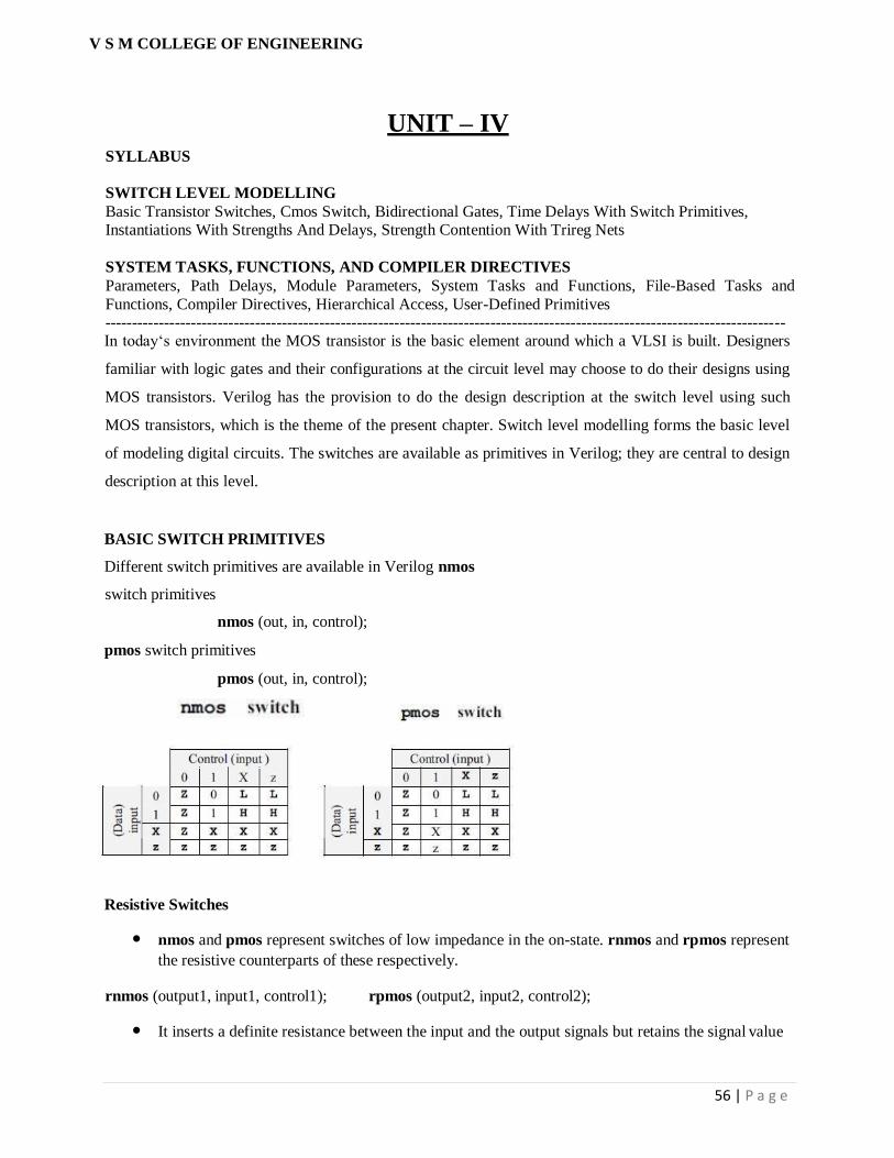
56 | P a g e
V S M COLLEGE OF ENGINEERING
SYLLABUS
UNIT – IV
SWITCH LEVEL MODELLING
Basic Transistor Switches, Cmos Switch, Bidirectional Gates, Time Delays With Switch Primitives, Instantiations With Strengths And Delays, Strength Contention With Trireg Nets
SYSTEM TASKS, FUNCTIONS, AND COMPILER DIRECTIVES
Parameters, Path Delays, Module Parameters, System Tasks and Functions, File-Based Tasks and
Functions, Compiler Directives, Hierarchical Access, User-Defined Primitives ------------------------------------------------------------------------------------------------------------------------------- In today‘s environment the MOS transistor is the basic element around which a VLSI is built. Designers
familiar with logic gates and their configurations at the circuit level may choose to do their designs using
MOS transistors. Verilog has the provision to do the design description at the switch level using such
MOS transistors, which is the theme of the present chapter. Switch level modelling forms the basic level
of modeling digital circuits. The switches are available as primitives in Verilog; they are central to design
description at this level.
BASIC SWITCH PRIMITIVES
Different switch primitives are available in Verilog nmos
switch primitives
nmos (out, in, control);
pmos switch primitives
pmos (out, in, control);
Resistive Switches
nmos and pmos represent switches of low impedance in the on-state. rnmos and rpmos represent
the resistive counterparts of these respectively.
rnmos (output1, input1, control1); rpmos (output2, input2, control2);
It inserts a definite resistance between the input and the output signals but retains the signal value
57 | P a g e
V S M COLLEGE OF ENGINEERING
The rpmos and rnmos switches function as unidirectional switches; the signal flow is from the
input to the output side.
strength levels
Output-side strength levels for different input-side strength values of rnmos, rpmos, and rcmos
switches
pullup and pulldown
A MOS transistor functions as a resistive element when in the active state. Realization of
resistance in this form takes less silicon area in the IC as compared to a resistance realized
directly. pullup and pulldown represent such resistive elements.
pullup (x);
Here net x is pulled up to the supply1 through a resistance.
pulldown(y);
pulls y down to the supply0 level through a resistance.
The pullup and pulldown primitives can be used as loads for switches or to connect the unused input
ports to VCC or GND, respectively.
CMOS SWITCH
A CMOS switch is formed by connecting a PMOS and an NMOS switch in parallel – the input
leads are connected together on the one side and the output leads are connected together on the
other side.
The CMOS switch is instantiated as shown below.
cmos csw (out, in, N_control, P_control );
BI-DIRECTIONAL GATES
Verilog has a set of primitives for bi-directional switches as well. They connect the nets on either
side when ON and isolate them when OFF. The signal flow can be in either direction
tran and rtran
The tran gate is a bi-directional gate of two ports. When instantiated, it connects the two ports
directly.
tran (s1, s2);
connects the signal lines s1 and s2. Either
line can be input, inout or output. rtran is
the resistive counterpart of tran.
58 | P a g e
V S M COLLEGE OF ENGINEERING
tranif1 and rtranif1
tranif1 is a bi-directional switch turned ON/OFF through a control line(c). It is in the ON-state
when the control signal is at 1 (high) state
tranif1 (s1, s2, c );
tranif0 and rtranif0
tranif0 and rtranif0 are again bi-directional switches. The switch is OFF if the control line is in
the 1 state, and it is ON when the control line is in the 0 state.
tranif0 (s1, s2, c);
TIME DELAYS WITH SWITCH PRIMITIVES
nmos g1 (out, in, ctrl );
has no delay associated with it. The instantiation
nmos (delay1) g2 (out, in, ctrl );
has delay1 as the delay for the output to rise, fall, and turn OFF.
nmos (delay_r, delay_f) g3 (out, in, ctrl ); has delay_r as the rise-time for the
output. delay_f is the fall-time for the output. The
turn-off time is zero.
nmos (delay_r, delay_f, delay_o) g4 (out, in, ctrl ); has delay_r as the rise-time for
the output. delay_f is the fall-time for the output delay_o
is the time to turn OFF when the control signal ctrl goes from 0 to 1.
Delays can be assigned to the other uni-directional gates in a similar manner.
Bi-directional switches do not delay transmission – their rise- and fall-times are zero.
They can have only turn-on and turn-off delays associated with them.
tran has no delay associated with it.
tranif1 (delay_r, delay_f) g5 (out, in, ctrl );
When control changes from 0 to 1, the switch turns on with a delay of delay_r. When control changes
from 1 to 0, the switch turns off with a delay of delay_f.
transif1 (delay0) g2 (out, in, ctrl );
represents an instantiation with delay0 as the delay for the switch to turn on when control changes from 0
to 1, with the same delay for it to turn off when control changes from 1 to 0

59 | P a g e
V S M COLLEGE OF ENGINEERING
INSTANTIATIONS WITH STRENGTHS AND DELAYS
nmos (strong1, strong0) (delay_r, delay_f, delay_o ) gg (s1, s2, ctrl) ; rnmos, pmos,
and rpmos switches too can be instantiated in the general form in the same manner. The
general instantiation for the bi-directional gates too can be done similarly.
STRENGTH CONTENTION WITH TRIREG NETS
nets declared as trireg can have capacitive storage. Such storage can be assigned one of three
strengths – large, medium, or small.
Driving such a net from different sources can lead to contention
PARAMETERS
Constants signifying timing values, ranges of variables, wires, etc., can be specified in
terms of assigned names. Such assigned names are called parameters.
Two types of parameters are of use in modules
Parameters related to timings, time delays, rise and fall times, etc., are technology-
specific and used during simulation. Parameter values can be assigned or overridden with
the keyword ―specparam‖ preceding the assignments.
Parameters related to design, bus width, and register size are of a different category. They
are related to the size or dimension of a specific design; they are technology-independent.
Assignment or overriding is with assignments following the keyword ―defparam‖.
PATH DELAYS
Verilog has the provision to specify and check delays associated with total paths – from any input to
any output of a module. Such paths and delays are at the chip or system level. They are referred to
as ―module path delays.‖
Specify Blocks
Module paths are specified and values assigned to their delays through specify
blocks. They are used to specify rise time, fall time, path delays pulse widths.
specify
specparam rise_time = 5, fall_time = 6;
(a =>b) = (rise_time, fall_time);
(c => d) = (6, 7);
endspecify
Module Paths
60 | P a g e
V S M COLLEGE OF ENGINEERING
Module paths can be specified in different ways inside a specify block. The simplest has the form
A*>B
Here ―A‖ is the source and ―B‖ the destination.
specify
(a,b*>s)=1; (a,b*>ca)=2;
endspecify
Conditional Pin-to-Pin Delays
The pin to pin path of a signal may change depending on the value of another signal; in turn the
number of circuit elements in the alternate path may differ.
specify if(f==2'b00)(a=>d)=1;
if(f >2'b00)(a=>d)=2;
(b,cci*>co)=1; endspecify
MODULE PARAMETERS
Module parameters are associated with size of bus, register, memory, ALU, and so on. They can
be specified within the concerned module but their value can be altered during instantiation. The
alterations can be brought about through assignments made with defparam. Such defparam
assignments can appear anywhere in a module.
SYSTEM TASKSANDFUNCTIONS
A ―$‖ sign preceding a word or a word group signifies a system task or a system function
Output Tasks
$monitor and $display
Display Tasks
The $display task, whenever encountered, displays the arguments in the desired format; and the
display advances to a new line. $write task carries out the desired display but does not advance to the new
line
$strobe Task
When a variable or a set of variables is sampled and its value displayed, the $strobe task can be
used; it senses the value of the specified variables and displays them.
$monitor Task
$monitor task is activated and displays the arguments specified whenever any of the arguments
changes
61 | P a g e
V S M COLLEGE OF ENGINEERING
$stop and $finish Tasks
The $stop task suspends simulation.
$finish stops simulation, closes the simulation environment, and reverts to the operating system.
$random Function
One can start with a seed number (optional) and generate a random number repeatedly. Such
random number sequences can be fruitfully used for testing.
FILE-BASED TASKS AND FUNCTIONS
To carry out any file-based task, the file has to be opened, reading, writing, etc., completed and
the file closed. The keywords for all file-based tasks start with the letter f to distinguish them
from the other tasks
All the system tasks to output information can be used to output to a file. $display, $strobe,
$monitor, etc., are of this category. The respective keywords to output to the file are
$fdisplay, $fstrobe, $fmonitor.
The first field of the task statement is an argument – the file descriptor. The subsequent fields are
identical to the corresponding nonfile tasks.
COMPILER DIRECTIVES
They allow for macros, inclusion of files, and timescale-related parameters for simulation. All
compiler directives are preceded by the ‗`‘.
`define Directive
The `define directive is used to define and associate the desired text with the macro name
`define add 2'b00
Time-Related Tasks
The `timescale compiler directive allows the time scale to be specified for the design. The
`timescale directive has two components
`timescale 1 ms/100 μs
HIERARCHICAL ACCESS
A Verilog design will normally have a module or two at the apex level. A number of modules and
UDPs will be instantiated within it.
$display("fad.a = %0d, fad.b = %0d, fad.fad = %0d", fad.a,fad.b,fad.fad);
USER-DEFINED PRIMITIVES (UDP)
62 | P a g e
V S M COLLEGE OF ENGINEERING
The primitives available in Verilog are all of the gate or switch types. Verilog has the provision
for the user to define primitives – called ―user defined primitive (UDP)‖ and use them.
A UDP can be defined anywhere in a source text and instantiated in any of the modules. Their
definition is in the form of a table in a specific format.
UDPs are basically of two types – combinational and sequential. A combinational UDP is used to
define a combinational scalar function and a sequential UDP for a sequential function
Combinational UDPs
A combinational UDP accepts a set of scalar inputs and gives a scalar output. An inout
declaration is not supported by a UDP.
The UDP definition is on par with that of a module; that is, it is defined independently like a
module and can be used in any other mo primitive udp_and (out, in1, in2); output out;
Sequential UDPs
Any sequential circuit has a set of possible states. When it is in one of the specified states, the
next state to be taken is described as a function of the input logic variables and the present state A
sequential UDP can accommodate all these.
Primitive dff_pos(q,din,clk,clr);
Output q;
input din,clk,clr;
reg q;
table
// din clk clr qp qn Whatever be the present
0 (01) 0: ?: 0; // state of the output, at the
1 (01) 0: ?: 1; // positive edge of clk input
? (10) 0: ?: -; // value is latched and
end table end primitive
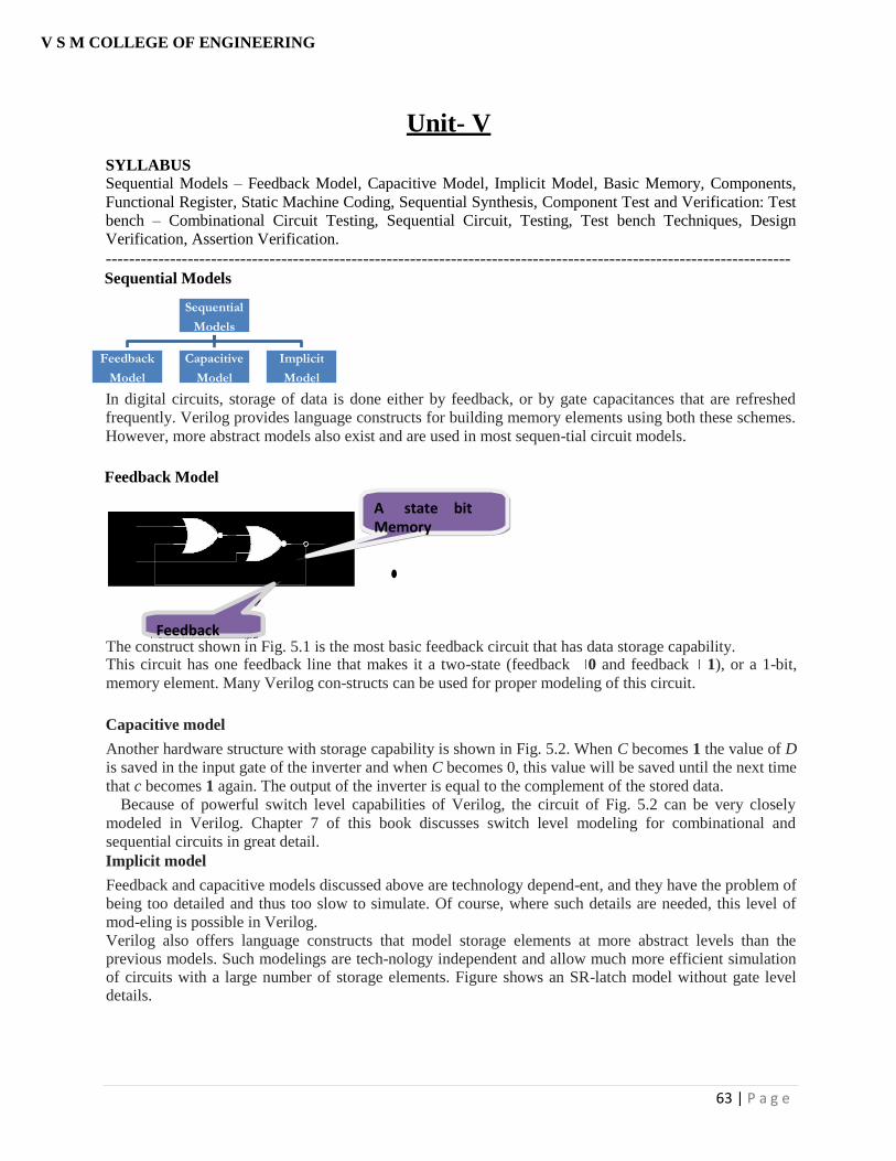
V S M COLLEGE OF ENGINEERING
63 | P a g e
Unit- V
SYLLABUS
Sequential Models – Feedback Model, Capacitive Model, Implicit Model, Basic Memory, Components,
Functional Register, Static Machine Coding, Sequential Synthesis, Component Test and Verification: Test
bench – Combinational Circuit Testing, Sequential Circuit, Testing, Test bench Techniques, Design
Verification, Assertion Verification.
--------------------------------------------------------------------------------------------------------------------- Sequential Models
In digital circuits, storage of data is done either by feedback, or by gate capacitances that are refreshed
frequently. Verilog provides language constructs for building memory elements using both these schemes.
However, more abstract models also exist and are used in most sequen-tial circuit models.
Feedback Model
The construct shown in Fig. 5.1 is the most basic feedback circuit that has data storage capability. This circuit has one feedback line that makes it a two-state (feedback 0 and feedback 1), or a 1-bit,
memory element. Many Verilog con-structs can be used for proper modeling of this circuit.
Capacitive model
Another hardware structure with storage capability is shown in Fig. 5.2. When C becomes 1 the value of D
is saved in the input gate of the inverter and when C becomes 0, this value will be saved until the next time
that c becomes 1 again. The output of the inverter is equal to the complement of the stored data.
Because of powerful switch level capabilities of Verilog, the circuit of Fig. 5.2 can be very closely
modeled in Verilog. Chapter 7 of this book discusses switch level modeling for combinational and
sequential circuits in great detail.
Implicit model
Feedback and capacitive models discussed above are technology depend-ent, and they have the problem of
being too detailed and thus too slow to simulate. Of course, where such details are needed, this level of
mod-eling is possible in Verilog.
Verilog also offers language constructs that model storage elements at more abstract levels than the previous models. Such modelings are tech-nology independent and allow much more efficient simulation of circuits with a large number of storage elements. Figure shows an SR-latch model without gate level details.
Implicit
Model
Capacitive
Model
Feedback
Model
Sequential
Models
A state bit Memory
Feedback
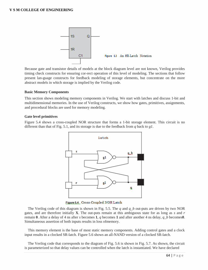
V S M COLLEGE OF ENGINEERING
64 | P a g e
Because gate and transistor details of models at the block diagram level are not known, Verilog provides
timing check constructs for ensuring cor-rect operation of this level of modeling. The sections that follow
present lan-guage constructs for feedback modeling of storage elements, but concentrate on the more
abstract models in which storage is implied by the Verilog code.
Basic Memory Components
This section shows modeling memory components in Verilog. We start with latches and discuss 1-bit and
multidimensional memories. In the use of Verilog constructs, we show how gates, primitives, assignments,
and procedural blocks are used for memory modeling.
Gate level primitives
Figure 5.4 shows a cross-coupled NOR structure that forms a 1-bit storage element. This circuit is no
different than that of Fig. 5.1, and its storage is due to the feedback from q back to g1.
The Verilog code of this diagram is shown in Fig. 5.5. The q and q_b out-puts are driven by two NOR
gates, and are therefore initially X. The out-puts remain at this ambiguous state for as long as s and r
remain 0. After a delay of 4 ns after s becomes 1, q becomes 1 and after another 4 ns delay, q_b becomes0.
Simultaneous assertion of both inputs results in loss ofmemory.
This memory element is the base of most static memory components. Adding control gates and a clock
input results in a clocked SR-latch. Figure 5.6 shows an all-NAND version of a clocked SR-latch.
The Verilog code that corresponds to the diagram of Fig. 5.6 is shown in Fig. 5.7. As shown, the circuit
is parameterized so that delay values can be controlled when the latch is instantiated. We have declared
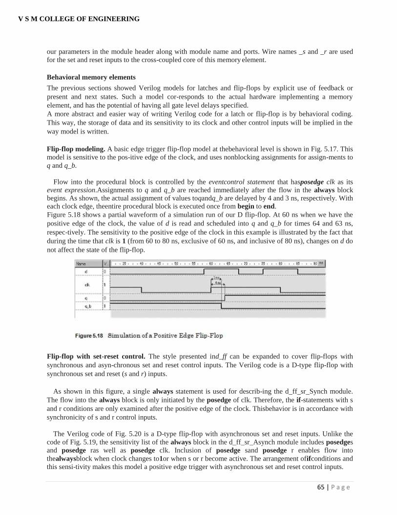
V S M COLLEGE OF ENGINEERING
65 | P a g e
our parameters in the module header along with module name and ports. Wire names _s and _r are used
for the set and reset inputs to the cross-coupled core of this memory element.
Behavioral memory elements
The previous sections showed Verilog models for latches and flip-flops by explicit use of feedback or
present and next states. Such a model cor-responds to the actual hardware implementing a memory
element, and has the potential of having all gate level delays specified.
A more abstract and easier way of writing Verilog code for a latch or flip-flop is by behavioral coding.
This way, the storage of data and its sensitivity to its clock and other control inputs will be implied in the
way model is written.
Flip-flop modeling. A basic edge trigger flip-flop model at thebehavioral level is shown in Fig. 5.17. This
model is sensitive to the pos-itive edge of the clock, and uses nonblocking assignments for assign-ments to
q and q_b.
Flow into the procedural block is controlled by the eventcontrol statement that hasposedge clk as its
event expression.Assignments to q and q_b are reached immediately after the flow in the always block begins. As shown, the actual assignment of values toqandq_b are delayed by 4 and 3 ns, respectively. With each clock edge, theentire procedural block is executed once from begin to end.
Figure 5.18 shows a partial waveform of a simulation run of our D flip-flop. At 60 ns when we have the
positive edge of the clock, the value of d is read and scheduled into q and q_b for times 64 and 63 ns,
respec-tively. The sensitivity to the positive edge of the clock in this example is illustrated by the fact that
during the time that clk is 1 (from 60 to 80 ns, exclusive of 60 ns, and inclusive of 80 ns), changes on d do
not affect the state of the flip-flop.
Flip-flop with set-reset control. The style presented ind_ff can be expanded to cover flip-flops with
synchronous and asyn-chronous set and reset control inputs. The Verilog code is a D-type flip-flop with
synchronous set and reset (s and r) inputs.
As shown in this figure, a single always statement is used for describ-ing the d_ff_sr_Synch module.
The flow into the always block is only initiated by the posedge of clk. Therefore, the if-statements with s
and r conditions are only examined after the positive edge of the clock. Thisbehavior is in accordance with
synchronicity of s and r control inputs.
The Verilog code of Fig. 5.20 is a D-type flip-flop with asynchronous set and reset inputs. Unlike the
code of Fig. 5.19, the sensitivity list of the always block in the d_ff_sr_Asynch module includes posedges
and posedge ras well as posedge clk. Inclusion of posedge sand posedge r enables flow into
thealwaysblock when clock changes to1or when s or r become active. The arrangement ofifconditions and
this sensi-tivity makes this model a positive edge trigger with asynchronous set and reset control inputs.
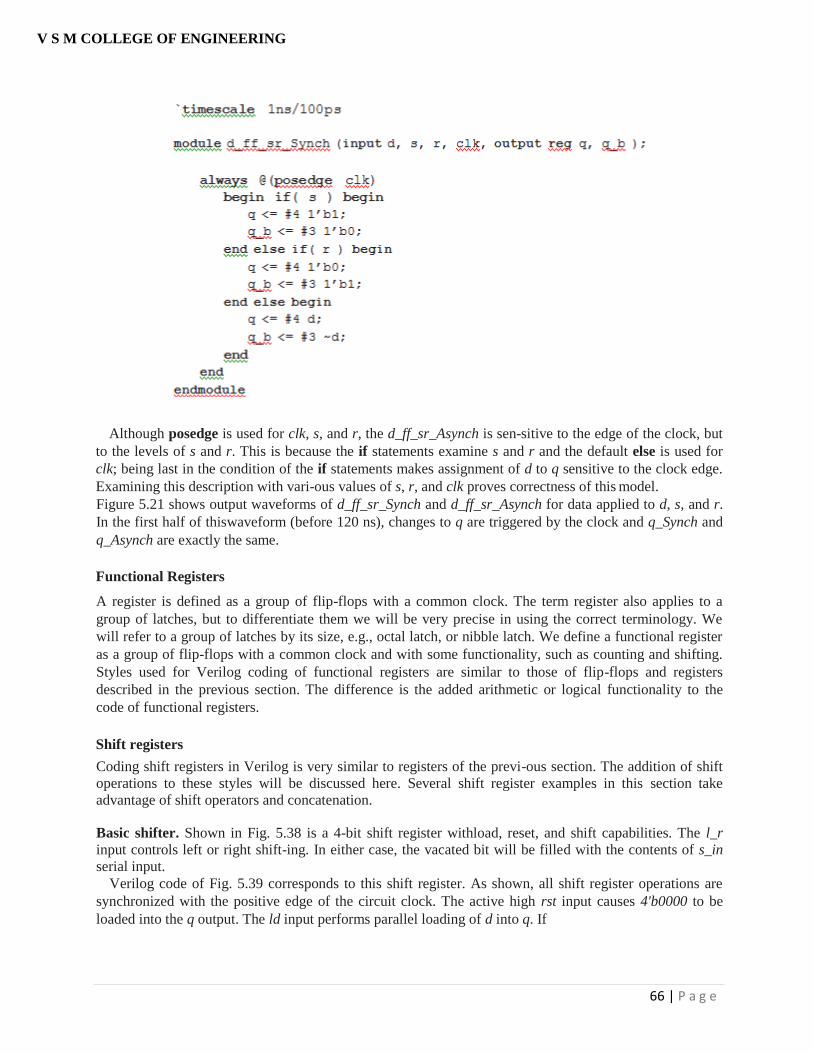
V S M COLLEGE OF ENGINEERING
66 | P a g e
Although posedge is used for clk, s, and r, the d_ff_sr_Asynch is sen-sitive to the edge of the clock, but
to the levels of s and r. This is because the if statements examine s and r and the default else is used for
clk; being last in the condition of the if statements makes assignment of d to q sensitive to the clock edge.
Examining this description with vari-ous values of s, r, and clk proves correctness of this model.
Figure 5.21 shows output waveforms of d_ff_sr_Synch and d_ff_sr_Asynch for data applied to d, s, and r.
In the first half of thiswaveform (before 120 ns), changes to q are triggered by the clock and q_Synch and
q_Asynch are exactly the same.
Functional Registers
A register is defined as a group of flip-flops with a common clock. The term register also applies to a
group of latches, but to differentiate them we will be very precise in using the correct terminology. We
will refer to a group of latches by its size, e.g., octal latch, or nibble latch. We define a functional register
as a group of flip-flops with a common clock and with some functionality, such as counting and shifting.
Styles used for Verilog coding of functional registers are similar to those of flip-flops and registers
described in the previous section. The difference is the added arithmetic or logical functionality to the
code of functional registers.
Shift registers
Coding shift registers in Verilog is very similar to registers of the previ-ous section. The addition of shift
operations to these styles will be discussed here. Several shift register examples in this section take
advantage of shift operators and concatenation.
Basic shifter. Shown in Fig. 5.38 is a 4-bit shift register withload, reset, and shift capabilities. The l_r
input controls left or right shift-ing. In either case, the vacated bit will be filled with the contents of s_in
serial input.
Verilog code of Fig. 5.39 corresponds to this shift register. As shown, all shift register operations are
synchronized with the positive edge of the circuit clock. The active high rst input causes 4'b0000 to be
loaded into the q output. The ld input performs parallel loading of d into q. If
V S M COLLEGE OF ENGINEERING
67 | P a g e
neither rst nor ld are active, l_r determines left or right shifting. Left shifting is performed by
concatenating s_in to the right of q[2:0] form-ing a 4-bit vector that is clocked into q[3:0]. Similarly, for
right shifting, a 4-bit vector is formed by concatenating s_in to the left of q[3:1]. In this case s_in goes
into q[3], and q[3], q[2], and q[1] go into q[2], q[1], and q[0], respectively, causing the right shifting of
q. All operations of this circuit are done in an always block that is sensitive to the positive edge of the
circuit clock. A nesting of if-else statements handles assignments to the q output. The lastelsecovers all
conditions not mentioned in the previ-ous if statements. This technique guarantees that all conditions are
taken care of by the if statement, and leaves no room for ambiguities.
5.3.1.2 Universal shift register. The Verilog code of auniversal shift register with bidirectional io. The
circuit has s1, s0 inputs forming a 2-bit number ranging from 3 to 0. The shifter does nothing, shifts right,
shifts left, or performs a parallel load depending on the value of {s1, s0}. The synchronous rst input resets
the shifter.
Because this circuit has a bidirectional inout port, we have declared q_int to hold the shift register
output at all times. Inside analwaysblock that is sensitive to the positive edge of the clock, assignments to
q_int take place. If rst is1, this variable is set to 0. Otherwise, acase
Basic Shifter Verilog Code
`timescale 1ns/100ps
module shift_reg (input [3:0] d, input clk, ld, rst, l_r, s_in, output reg [3:0]
q);
always @( posedge clk ) begin if( rst )
#5 q <= 4’b0000; else if( ld )
#5 q <= d; else if( l_r )
#5 q <= {q[2:0], s_in}; else
#5 q <= {s_in, q[3:1]};
End endmodule
V S M COLLEGE OF ENGINEERING
68 | P a g e
Universal Shift Register
`timescale 1ns/100ps
module shift_reg (input clk, rst, r_in, l_in, en, s1, s0, inout [7:0] io);
reg [7:0] q_int;
assign io = (en) ? q_int : 8’bz; always @( posedge clk ) begin
if( rst )
#5 q_int = 8’b0; else
case ( {s1,s0} )
2’b01 : // Shift right
q_int <= { r_in, q_int[7:1] }; 2’b10 : // Shift left
q_int <= { q_int[6:0], l_in }; 2’b11 : // Parallel load
q_int = io;
default : // Do nothingq_int <= q_int;
endcase
end
endmodule
statement uses {s1, s0} to decide value assigned to q_int. The case statement uses the default alternative to
cover {s1, s0} of 2’b00 and all possible ambiguous values. This default alternative is like the else of the
previous example, which guarantees that all conditions areaccounted for.
The ionet is the bidirectional port of this shift register. When {s1, s0} is 2’b11 (parallel loading the shift-
register), io is read and put into q_int. For outputting through io, an assign statement assigns q_int or eight
Zs to this bidirectional bus. Ifenis 1 q_intis put oni0, and if it is 0,8’bZdrives io. An external device
wanting to drive io from outside of this module can only do so when en is 0.
State Machine Coding
Coding styles presented so far can further be generalized to cover finite state machines of any type. This
section shows coding for Moore and Mealy state machines. The examples we will use are simple sequence
detectors, yet they represent coding for complex control-heavy digital cir-cuits, or the controller part of an
RT level design.
Moore machines
A Moore machine is a state machine in which all outputs are fully syn-chronized with the circuit clock. In
the state diagram form, each state of the machine specifies its output(s) independent of circuit inputs. In
the Verilog code of a Moore state machine, only circuit state variables participate in the output expression
of the circuit.
A 101 Moore sequence detector with its corre-sponding block diagram related to its Verilog coding. The
machine searches for 101 on its input and when received, the output of the cir-cuit becomes 1 and remains
at this level for a complete clock period. As shown in the state diagram, when the machine reaches the
got101 state, its output becomes 1.
The block diagram of the Verilog coding that will be used for this machine is also shown An always
block that handles state transitions and clocking generates current state of the machine. This variable is
used by an assign statement that generates the z output of the circuit.
The Verilog code of moore_detector. We have used a localparam declaration to assign values to the
states of the machine.
V S M COLLEGE OF ENGINEERING
69 | P a g e
Because our machine has four states, 2-bit parameters are used for the state names. Furthermore, the
declaration part of the moore_detector module declares current as a 2-bit reg. This variable is used for
hold-ing the current state of the machine.
The always block of Fig. 5.54 implements a positive edge trigger sequential block with a synchronous
reset (rst) input. If rst is active, cur-rent is set to reset, otherwise, acasestatement assigns next state
valuesto current. Next states of the machine are decided by the current state that is the case expression,
and input values.
Each state of the machine is implemented by a case alternative, and its next state transitions are
implemented by if statements conditioned by the x input of the circuit. Figure 5.55 shows a
correspondence between the got10 state of the machine and its Verilog coding. This state branches out to
got101 or reset depending on x. The output of the circuit is imple-mented by a separate assign statement
that puts a 1 on z when cur-rent is got101.
Because this is a Moore machine, the condition for asserting the output of the circuit only includes the
current variable, and circuit input(s) are not included. Figure 5.56 shows another Moore machine example.
This machine searches for 110 or 101 sequences on its x input. The search allows overlapping sequences.
The Verilog code of the Moore machine of Fig. 5.56 is shown in Fig. 5.57. We are using `define
directives for assigning values to the state names. Note that using names is only for readability purposes,
and instead of using `define or localparam, as in the previous example, state values could be used in the
case statement of this Verilog code.
The Verilog code shown here implements a state machine with asyn-chronous active high reset (rst)
input. For this purpose, posedgerst is included in the sensitivity list of the always block. In this always
block, the last case alternative is the default case that accounts.
Mealy machines
A Mealy machine is different from a Moore machine in that its output(s) depend on its current state
and inputs while in that state. State tran-sitions, clocking, and resetting the machine are not
different from those of a Moore machine, and the same coding techniques are used for describing
them.
V S M COLLEGE OF ENGINEERING
70 | P a g e
a 101 Mealy sequence detector and its correspon-ding Verilog code block diagram. This circuit has a
synchronous rst input that resets the machine to its reset state.
The Verilog code of Fig. 5.59 corresponds to this Mealy machine. A 2-bit localparam construct is used
for defining the states of this machine. Because the machine has three states and two state variables are
used to represent them, one combination (i.e., 11) of the state variables becomes unused. As in the
previous example, the default in the case statement of this Verilog code handles this unspecified
combination and ambiguous values that may appear on current.
The coding of the states and output of this machine are illustrated in Fig. 5.60. Each state is specified by
a case alternative of a case state-ment for which current is its case expression. Transitions to the next
states of the machine are handled by if-else statements. The output of the machine is set to 1 using an
assign statement that uses a conditional expression on its right-hand side. This conditional expression uses
the circuit input as well as the current state of the machine.
Sequential Synthesis
The process of synthesis involves describing a hardware in an accept-able form for the synthesis tool to recognize and then specifying a target library representing available low-power components to map to. The target library has combinational and sequential components. Exactly how a synthesizable Verilog input description translates to hardware depends on the specific target library. For example, if an input descrip-tion involves a latch and the target library does not have a latch, then a latch will be build using
gates or logic functions that are available in the target library.
Verilog models described in this chapter, except those with initial statements loading a memory, are
synthesizable. In this section, we will go back and look at several typical styles of coding and discuss the
kind of hardware that they synthesize to.
Latch models
Except for the delay values, the latch Verilog description of Fig. 5.14 is synthesizable. If a target hardware
library contains a D-latch, it will be used for mapping this description, otherwise it will be built by wiring
existing target hardware parts.
an Altera field programmable gate array (FPGA) logic element that has several logic gates, a look-up
table, and a flip-flip. The implementation of a D-latch is highlighted in this diagram. The gray areas are
V S M COLLEGE OF ENGINEERING
71 | P a g e
those parts of the logic element (LE) that are actually used for our latch. As shown, the latch is
implemented by programming the look-up table (the rectangular box with A, B, C, D inputs). The output
of this table is the latch output and also feeds back to the table to cause the latching action. Note in this
figure that the flip-flop (the rectangu-lar box on the right) of the FPGA logic element is not used.
Testbench
Verilog simulation environments provide tools for graphical or textual display of simulation results. Some
simulation environments go fur-ther, and provide graphical tools for editing input test data to a design
module that is being tested. Such tools are referred to as waveform edi-tors, and are usually good for small
designs. They become too complex to use for a design with many busses and control signals. Another
prob-lem with waveform editors is that each simulation environment uses a different procedure for
waveform editing, and moving from one simu-lator to another requires relearning a whole new set of
procedures.
This problem can be alleviated by use of Verilog testbenches. A Verilog testbench is a Verilog module
that instantiates an MUT, applies data to it, and monitors its output. Because a testbench is in Verilog, it
can go from one simulation environment to another. A module and its corresponding testbench form a
simulation model in which MUT is tested for the same input data regardless of what simulation
environment is used.
To facilitate development of testbenches, some simulation environ-ments provide testbench tools that
automatically generate a template testbench. Such tools also provide ways of inserting templates for gen-
eration of test data for applying them to MUT. Using templates is help-ful, but a designer must understand
testbenches and language constructs that are used for testing a design module. In the next two sub-sections
basics of testbenches are discussed.
Combinational circuit testing
Developing a testbench for a combinational circuit is straight forward, however selection of data and how
much testing should be done depends on the MUT and its functionality.
Chapter 4 presented a simple arithmetic logical unit (ALU) (Fig. 4.63) that we use here to test. Module
header and declarations of its ports are repeated in Fig. 6.1 for reference. The alu_4bit module is a four
func-tion ALU. Data inputs are a and b, and its function input is f. In addi-tion to its y data output, the
ALU generates parity (p), overflow (ov), and compare outputs.
A testbench for alu_4bit is shown in Fig. 6.2. Variables correspon-ding to inputs and outputs of the
module under test are declared in the testbench. Variables connecting to the inputs are declared as reg and
outputs as wire. Instantiation of alu_4bit shown in the testbench asso-ciates local regs and wires with the
ports of this module.
Variables that are associated with the inputs of alu_4bit have been given initial values when declared.
Application of data to the b data input and oe output-enable of ALU are done in an initial statement. For
the first 60 ns every 20 ns, a new value is assigned to b. The initial block then waits for 80 ns, disables the
ALU output by setting oe to 0, and after 20 ns it finishes the simulation. This last 20 ns wait, allows effects
of the last input change to be shown in simulation results.
Application of data to the f input of alu_4bit is done in an always state-ment. Starting with the initial
value of 0, f is increment by 1 every 23 ns.
The $finish statement in the initial block of the testbench is reached at 160 ns. At this time all active
procedural blocks stop and simulation terminates. Figure 6.3 shows simulation results of the alu_4bit
module.
Throughout the simulation a remains constant, and b changes from 6 to B and then to E at 40 ns. The f
function input changes every 23 ns causing various ALU functions to be examined. At 140 ns, oe changes
to 0, causing the y output become Z.
V S M COLLEGE OF ENGINEERING
72 | P a g e
Sequential circuit testing
Testing sequential circuits involves synchronization of circuit clock with other data inputs. We use the
misr module of Chap. 5 for an example here. This circuit, repeated in Fig. 6.4 for reference, has a clock
input, a reset, data inputs, and outputs.
The circuit has a poly parameter that determines its signature and data compression. With each clock a new signature will be calculated with the new data and existing misr register data.
Figure 6.5 show a testbench for misr. As before, variables correspon-ding to the ports of MUT are
declared in the testbench. When misr is instantiated, these variables are connected to its actual ports. Our
misr instance also includes specification of its poly parameter.
The initial block of this testbench generates a positive pulse on rst that begins at 13 ns and ends at 63
ns. The timing is so chosen to cover at least one positive clock edge, so that the synchronous rst input can
initialize the misr register. The d_in data input begins with x, and is ini-tialized to 4’b1000 while rst is 1.
In addition to the initial block, the test_misr module includes two always blocks that generate data
ond_inandclk. Clock is given a peri-odic signal that toggles every 11 ns. The misr d_in input is assigned a
new value every 37 ns. In order to reduce chance of several inputs chang-ing at the same time, we usually
use prime numbers for timing of sequential circuit inputs.
module #(parameter [3:0] poly=0) misr (input clk, rst, input [3:0] d_in, output reg
[3:0] d_out );
always @( posedge clk ) if( rst )
d_out =4’b0000;
else
d_out = d_in ^ ({4{d_out[0]}} & poly) ^ {1’b0,d_out[3:1]};
endmodule
module test_misr; reg clk=0, rst=0; reg [3:0] d_in;
wire [3:0] d_out;
misr #(4’b1100) MUT ( clk, rst, d_in, d_out );
initial begin
#13 rst=1’b1; #19 d_in=4’b1000; #31 rst=0’b0;
#330 $finish;
end
always #37 d_in = d_in + 3;
always #11 clk = ~clk;
endmodule
As shown starting at 40 ns with this and every positive edge of clk, a new signature is generated in misr.
Since prior to time 80 ns, misr is reset to0, the first signature that happens at 80 ns is the sameas d_in.
Testbench Techniques
Various Verilog coding techniques for generation of test data and observ-ing circuit responses are
discussed in this section. We use state machines of Chap. 5 for our test modules. The first example is a
101 Moore detec-tor circuit depicted
We have used a coding style that is somewhat different than that used. The z output becomes 1 in state d
when a sequence of 101 is detected onx. The circuit has a synchronous reset input.
V S M COLLEGE OF ENGINEERING
73 | P a g e
Test data
A testbench for moore_detector. As before, our testbench is a module with no ports. Within this module,
four pro-cedural blocks provide data for testing the state machine. Variables connected to inputs of MUT
and used on the left-hand sides in the pro-cedural blocks are declared as reg. Instead of initializing reg
variables when they are declared, we have used an initial block for this purpose. It is important to
initialize vari-ables, like clock, for which their old values are used for determining their new values. If not
done so, clock would start with value X and comple-menting it would never change its value. The always
block shown gen-erates a periodic signal with a period of 10 ns on clock.
Following the always block producing clock, another always block generates a periodic signal on x with
a period of 14 ns. The waveform generated on x may or may not be able to test our machine for a correct
101 sequence. However, periods ofclockandxcan be changed to makethis happen. With the timing used
here, the moore_detector output becomes 1 at 55 ns, and every 70 ns from then on.
Design Verification
The previous section discussed test techniques for testing a Verilog design. We presented several methods
of test data generation and test application, and suggested ways of observing and inspecting test results.
Stimuli generation and response analysis require significant efforts on the part of a hardware designer.
Learning correct test techniques is good, but automation of either of these procedures will be very useful
for a design engineer.
Formal verification is a way of automating design verification by elim-inating testbenches and problems
associated with their data generation and response observation. In formal verification, a designer writes
prop-erties to check his or her design. Formal verification tools do not per-form simulation, but come up
with a Yes/No answer for every property the design is being checked for. Although this method of design
verifica-tion helps discover many design errors, most designs still need testbench
development and simulation for validating that their Verilog code indeed functions as expected. In other
words, an all ―Yes‖ answers to design properties checked by formal verification tools is still not enough.
Instead of eliminating data generation and response observation (like the formal verification tools), a
step in the direction of automating design validation is to reduce or eliminate efforts needed for analyzing
output responses. For this purpose assertion verification is used. Assertion ver-ification adds monitors to a
design to improve its observability. While the design is being simulated with its testbench data, assertion
moni-tors that represent certain design properties continuously check for cor-rect design behavior by
validating these properties. If the simulation data leads into conditions that indicate to an assertion monitor
that the design is misbehaving, the monitor is said to fire to alert the designer of the problem.
As mentioned, we still need to develop a testbench and careful plan-ning of test inputs for the design
being tested is needed in assertion ver-ification. But, in many cases, assertions automatically check to
make sure events that occur in the design are as expected. This significantly reduces the need for
processing long output lists or waveforms.
Assertion Verification
Unlike simulation that a testbench or a human has to interpret the results, in assertion verification, in-code
monitors take the responsibil-ity of issuing a message if something happens that is not expected. In
Verilog, these monitors are modules, and they are instantiated in a design to check for certain design
properties. Instantiating an assertion module is not to be regarded as instantiation of a hardware module.
Instead, this kind of instantiation is more like an always-active proce-dure that continuously checks for
events in the design module.
The present set of assertion monitors are available in a library that is referred to as open verification
library (OVL). Designers can develop their own set of assertions, and use them in their designs. The
existing monitors check for values of signals, relation of several signals with each other, sequence of
V S M COLLEGE OF ENGINEERING
74 | P a g e
events, and expected patterns on vectors or groups of signals. For using assertions, a designer compiles
OVL and his or her own assertion library into a simulation library and makes this library available to
designs being verified. When a design is developed, assertions are placed at key points in the design to
check for key func-tionalities. When the design is being simulated as a stand-alone com-ponent, or in a
hierarchy of a larger design, the monitors check signals for their expected values. If a signal does not have
a value expected by a monitor, the assertion monitor displays a message and the time that the discrepancy
(violation of the property) has occurred. Usually, such messages appear in the simulation report area,
transcript, or console.
Assertion verification benefits
Ways in which placement of assertion monitors in a design are helpful are discussed here.
Designer discipline. When a designer places an assertion in a design,he or she is disciplining
him/herself to look into the design more care-fully and extract properties.
Observability. Assertions add monitoring points to a design that makeit more observable.
Formal verification ready. Assertions correspond to properties that areused in formal verification tools. Having inserted assertion monitors to a design, readies it for verification by a formal verification tool.
Executable comments. Assertion monitors can be regarded as commentsthat explain some features or
behavior of a design. These comments pro-duce messages when the behavior they are explaining is
violated.
Self-contained designs. A design with assertion monitors has the designdescription and its test procedure all in one Verilog module.