Embed Size (px)
Citation preview

06 June 2007 CAS, Sigtuna, SwedenDSP – Digital Signal Processing
Digital Signal Processing in RF Applications
Part I
Thomas Schilcher

RF applications
CAS, Sigtuna, SwedenDSP – Digital Signal Processing
T. Schilcher
06 June 2007 2
What are RF applications?
any application which measures properties of an RF field (amplitude, phase, frequency, …);typical frequencies in accelerators: MHz – tens of GHz
applications which process the measured quantities to control and regulate RF fields(feedback and feedforward)

RF applications
CAS, Sigtuna, SwedenDSP – Digital Signal Processing
T. Schilcher
06 June 2007 3
Typical RF applications
cavity field loops (amplitude and phase)klystron loops (amplitude and phase)tuner loops (cavity tuning)radial and phase loops (circular machines)“RF gymnastics” (bunch splitting and merging)
Accelerators:CW / pulsed machines
linear / circular machines
Application areas (examples):
electron/hadron/ion accelerators
normal-/superconducting RF systems
RF applications
CAS, Sigtuna, SwedenDSP – Digital Signal Processing
T. Schilcher
06 June 2007 4
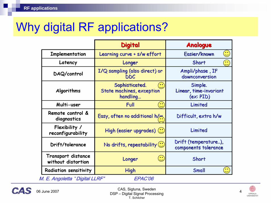
Why digital RF applications?

RF applications
CAS, Sigtuna, SwedenDSP – Digital Signal Processing
T. Schilcher
06 June 2007 5
Key components of digital RF applications
signal conditioning/ down conversion
digitizationamp./phase/I/Q detection
digital signal processing /algorithms
vector modulator/ up conversion/ amplification
RF signal
monitoring /control system
RF signal
acce
lera
tor /
pla
nt
LLRF looks very similar to many other applications, e.g. diagnostics (bunch-by-bunch feedback, position monitoring, …)
(feedback applications)
for feedback systems: ultimate error is dominated by the measurement process(systematic error, accuracy, linearity, repeatability, stability, resolution, noise)

RF applications
CAS, Sigtuna, SwedenDSP – Digital Signal Processing
T. Schilcher
06 June 2007 6
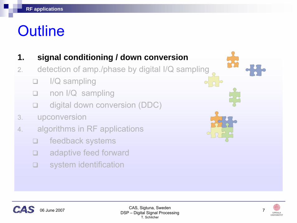
Outline1. signal conditioning / down conversion2. detection of amp./phase by digital I/Q sampling
I/Q samplingnon I/Q samplingdigital down conversion (DDC)
3. upconversion4. algorithms in RF applications
feedback systemsadaptive feed forwardsystem identification
RF applications
CAS, Sigtuna, SwedenDSP – Digital Signal Processing
T. Schilcher
06 June 2007 7
Outline1. signal conditioning / down conversion2. detection of amp./phase by digital I/Q sampling
I/Q samplingnon I/Q samplingdigital down conversion (DDC)
3. upconversion4. algorithms in RF applications
feedback systemsadaptive feed forwardsystem identification

RF applications
CAS, Sigtuna, SwedenDSP – Digital Signal Processing
T. Schilcher
06 June 2007 8
Signal conditioning / down conversionWhy down conversion of the RF signal?
ADC speeds are limited. It is not reasonable/possible today to digitize high-frequency carriers directly. (f>500 MHz)
ADC dynamic range is limited.
10 bit → 60 dB12 bit → 72 dB14 bit → 84 dB
ADC clock and aperture jitter become critical at high frequencies(especially for undersampling schemes)
RF mixers are essential for digital high frequency applications
often better: use analogue circuits in conjunctionwith the ADC to implement automated gain control (AGC)functions to ensure that this range is best used

RF applications
CAS, Sigtuna, SwedenDSP – Digital Signal Processing
T. Schilcher
06 June 2007 9
RF mixer (ideal)
mixer: linear time varying circuit, non-linear circuit (diodes…)
lower sideband
upper sideband
even ideal mixers produce two sidebands

RF applications
CAS, Sigtuna, SwedenDSP – Digital Signal Processing
T. Schilcher
06 June 2007 10
fLO
f +fLO RFf -fLO RF fRFfrequency
signalamplitude
fLO
f +fLO RFf -fLO RF fRFfIMAGE frequency
signalamplitude
ideal mixer: output is the multiplication of the two input signals
down conversion:RF, LO are high frequency inputsIF: lower intermediate frequency output
up conversion:IF is input, RF is output
RF mixer (ideal)
fLO
f +fLO IFf -fLO IFfIF
frequency
signalamplitude
lowersideband
uppersideband
RF applications
CAS, Sigtuna, SwedenDSP – Digital Signal Processing
T. Schilcher
06 June 2007 11
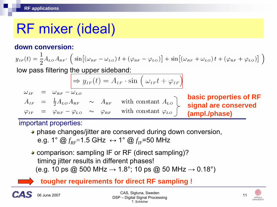
RF mixer (ideal)
low pass filtering the upper sideband:
important properties:phase changes/jitter are conserved during down conversion,e.g. 1° @ fRF=1.5 GHz ↔ 1° @ fIF=50 MHz
comparison: sampling IF or RF (direct sampling)?timing jitter results in different phases!
(e.g. 10 ps @ 500 MHz → 1.8°; 10 ps @ 50 MHz → 0.18°)
basic properties of RF signal are conserved (ampl./phase)
tougher requirements for direct RF sampling !
down conversion:

RF applications
CAS, Sigtuna, SwedenDSP – Digital Signal Processing
T. Schilcher
06 June 2007 12
RF mixer (real)real mixers = non linear devices
many undesired harmonics in frequency spectrum non-linearities in IF signal
filtering the output of a mixer might be necessarytake care about the introduced group delay by the filter trade off!
I-V curve of a diode

RF applications
CAS, Sigtuna, SwedenDSP – Digital Signal Processing
T. Schilcher
06 June 2007 13
Outline1. signal conditioning / down conversion2. detection of amp./phase by digital I/Q sampling
I/Q samplingnon I/Q samplingdigital down conversion (DDC)
3. upconversion4. algorithms in RF applications
feedback systemsadaptive feed forwardsystem identification

RF applications
CAS, Sigtuna, SwedenDSP – Digital Signal Processing
T. Schilcher
06 June 2007 14
direct amplitude phase detectors
analogue IQ detection
digital IQ sampling /Digital Down Conversion (DDC)
Amplitude and phase detection

RF applications
CAS, Sigtuna, SwedenDSP – Digital Signal Processing
T. Schilcher
06 June 2007 15
RF vector representationrepresentation of any sinusoidal RF signal: phasor
I: in-phase component
Q: quadrature-phase component
definition: positive frequencies ↔ counterclockwise rotating phasor
(assumption: we measure the vertical component with ADC)
(sometimes I/Q aredefined vice versa!)

RF applications
CAS, Sigtuna, SwedenDSP – Digital Signal Processing
T. Schilcher
06 June 2007 16
IQ sampling (1)
goal: monitor amplitude/phase (A/φ0) variations of incoming RF/IF signalpossible also to monitor I/Q at a reference time (reference phase)
“process” sampled I/Q values for comparison, i.e. rotate phasor back to reference phasor if phase advancebetween sampling is well known

RF applications
CAS, Sigtuna, SwedenDSP – Digital Signal Processing
T. Schilcher
06 June 2007 17
IQ sampling (2)sampling of RF/IF freq.: (i.e. 90° phase advance
between two samples)

RF applications
CAS, Sigtuna, SwedenDSP – Digital Signal Processing
T. Schilcher
06 June 2007 18
IQ sampling (3)
rotate corresponding I/Q vector by -90° / -180 ° / -270 ° in order to compare to initial I/Q values
rotation matrix with angle :
build up I/Q vector based on two successive samples
I/Q processing with sampling frequency fS

RF applications
CAS, Sigtuna, SwedenDSP – Digital Signal Processing
T. Schilcher
06 June 2007 19
IQ sampling (4)
general:
phase advance between consecutive samples:
1. relation between measured amplitudes and I/Q
2. rotation of to with angle :
3. rotation of to with angle :

RF applications
CAS, Sigtuna, SwedenDSP – Digital Signal Processing
T. Schilcher
06 June 2007 20
DC offsets of carrier frequencysamples are not exactly 90° apart (e.g. due to ADC clock jitter)
ripple on I/Q values with freq. of carrier ( e.g. fIF)
choosing phase advances “far” away from 90° can worsen signal to noise ratio
IQ sampling – potential problems (1)
“easily”detectable errors in IQ
demodulationrotated vector

RF applications
CAS, Sigtuna, SwedenDSP – Digital Signal Processing
T. Schilcher
06 June 2007 21
IQ sampling – potential problems (2)
differential non-linearities of ADCs
non-linearities of mixers
generate high harmonics of input carrier odd harmonics of carrier frequency are not distinguishable from carrier by IQ detection
errors difficult to detect in
IQ demodulation
example:IF fundamental with 20% of 3rd harmonic component
if input phase and amplitude changes, the distortion changesand can corrupt the measurement

RF applications
CAS, Sigtuna, SwedenDSP – Digital Signal Processing
T. Schilcher
06 June 2007 22
Non-IQ samplingrecall:
choose sampling frequency fS and IF frequency fIF such that:N, M: integersN samples in M IF periods
phase advance between two samples:
example: M=3 (IF periods), N=25
where
overestimated system of linear equationscan be solved by least mean square algorithm
sampling “whole” IF sinusoidal signal if M, N are properly chosen

RF applications
CAS, Sigtuna, SwedenDSP – Digital Signal Processing
T. Schilcher
06 June 2007 23
Non-IQ sampling (2)least mean square algorithm: minimize with respect to I,Q
if(sin and cos can be pre-calculated and stored in look-up tables)

RF applications
CAS, Sigtuna, SwedenDSP – Digital Signal Processing
T. Schilcher
06 June 2007 24
Non-IQ sampling (3)
• errors from DC offsets, clock jitter, ADC quantization, noise reduced• but more latency due to sampling M IF periods • trade-off between noise reduction and linearity improvement and low latency
choose M,N properly !
most harmonics no longer line up with IF signal !
M=15N=4

RF applications
CAS, Sigtuna, SwedenDSP – Digital Signal Processing
T. Schilcher
06 June 2007 25
Digital Down Conversion (DDC)(sometimes referred to as “Digital Drop Receiver” (DDR))
example: fIF = 40 MHzfS = 100 MHz (oversampling)signal BW = 1 MHzoutput sample rate of 2.5 MHz is fine!
reduce the amount of required subsequent processing of the signal without loss of any of the information carried by the IF signal
filtering and data reduction !
implementation on FPGA, DSP or ASICtwo classes of DDCs:
narrowband (decimation R≥32, → CIC filter [Cascaded Integrator Comb])wideband (decimation R<32, → FIR / multi-rate FIR filters)
Goal: shift the digitized band limited RF or IF signal from its carrierdown to baseband

RF applications
CAS, Sigtuna, SwedenDSP – Digital Signal Processing
T. Schilcher
06 June 2007 26
DDC (2)
Local Oscillator(Numerical Controlled Oscillator, NCO)Mixer (digital)Decimating Low Pass Filter(LPF)
DDC building blocks:NCO: direct digital frequency synthesizer (DDS)sine and cosine lookup table
digital mixers: “ideal” multipliers → two output frequencies(sum and difference freq. signals)
decimating low pass (anti alias) filter (often implemented as CIC and FIR)
inside DDC: three major sections

RF applications
CAS, Sigtuna, SwedenDSP – Digital Signal Processing
T. Schilcher
06 June 2007 27
NCO advantages:tuning word is programmable
frequencies up to nearly fS/2 (Nyquist) possible extremely fast “hopping speed” in tuning output frequency, phase-continuousfrequency hops with no over/undershoot or analog-related loop settling time anomalies.
NCO functionality:phase accumulator → calculate new phase @ fS with phase advance defined by tuning word. (NCO clock: sample rate fS)convert phase to amplitude(often done in ROM based sine lookup tables; either one full sin wave is stored or only a quarter with some math on the pointer increment) phase accumulator overflow → wrap around in circular lookup table
DDC building block: NCO
new freq.
f1 f2

RF applications
CAS, Sigtuna, SwedenDSP – Digital Signal Processing
T. Schilcher
06 June 2007 28
addendum: Direct Digital Synthesis (DDS)
DDS properties:produce an analog waveform by generating a time-varying signal in digital formsize of lookup table (phase to amp. conv.) is determined by:
number of table entries bit width of entries (determines amplitude output resolution)
output frequency:
example: N=32 bit ; fS=50 MHz df= 12 mHz
but: do we need 2N (8 bit entries→ 4 GByte!) entries in lookup table?
(M: tuning word, N: length in bits of phase accumulator)

RF applications
CAS, Sigtuna, SwedenDSP – Digital Signal Processing
T. Schilcher
06 June 2007 29
Direct Digital Synthesis (2)Phase truncation:
in order to save memory in lookup table:truncate phase before the lookup table!example: N=32: keep only upper most 12 bits,
truncate lower 20 bits
implications: introduce phase error which is periodic in timeresult in amplitude errors during phase to amplitude conversionphase truncation spurs
Output precompensation:sin(X)/X rolloff response due to DAC output spectrumwhich is quite significantprecompensate output before DAC with inverse sinc filter

RF applications
CAS, Sigtuna, SwedenDSP – Digital Signal Processing
T. Schilcher
06 June 2007 30
DDC building block: Cascaded Integrator Comb Filter (CIC)
(introduced by Eugene Hogenauer, 1981)
basic elements:
basic integrator basic comb
computationally efficient implementations of narrowband low pass filters (no multipliers needed!)multi-rate filter (decimation/interpolation)

RF applications
CAS, Sigtuna, SwedenDSP – Digital Signal Processing
T. Schilcher
06 June 2007 31
CIC filter (2)
FIR filter!(stable)
filter structure for decimating CIC:
filter structure for interpolating CIC:
D: differential delay
reference samplingrate for transfer function:always higher freq.
basic comb filter(referenced to the high input sample rate):

RF applications
CAS, Sigtuna, SwedenDSP – Digital Signal Processing
T. Schilcher
06 June 2007 32
example: decimating CIC (1st order)with integer decimation factor R
CIC: originate from the concept of a recursive running-sum filter(efficient form of a non-recursive moving average filter [boxcar filter])
boxcar filter, length N:(moving average)
How to understand CIC?
geometric sum

RF applications
CAS, Sigtuna, SwedenDSP – Digital Signal Processing
T. Schilcher
06 June 2007 33
How to understand CIC (2)recursive running-sum:
(alternate implementationof boxcar filter)
boxcar/recursive running-sum filters have the same transfer functionas a 1st order CIC (except: 1/N gain; general diff. delay D)
transfer function:
in many applications: boxcar followed by decimation R=N compare with1st order CIC:

RF applications
CAS, Sigtuna, SwedenDSP – Digital Signal Processing
T. Schilcher
06 June 2007 34
applications:anti-aliasing filtering prior to decimationtypically employed in applications that have a large excess sample rate.→ system sample rate is much larger than the bandwidth occupied by the signal(remember example: fIF = 40 MHz, fS = 100 MHz, signal BW = 1 MHz)
resources: uses additions and subtractions onlyfrequency response: evaluate H(z) at
CIC properties
frequency response with respect to the output frequency
design parameter D determineslocations of zeros:
(k: integer)

RF applications
CAS, Sigtuna, SwedenDSP – Digital Signal Processing
T. Schilcher
06 June 2007 35
CIC properties (2)DC gain:net gain of CIC at DC: (RD)M
→ Each additional integrator must add another bits width of (RD) for each stage(implementation with two's complement (nonsaturating) arithmetic due tooverflows at each integrator)
frequency response: (M: number of CIC stages, D: differential delay)
important characteristic:shape of the filter responsechanges very little as afunction of the decimationratio R
plot relative freq. response

RF applications
CAS, Sigtuna, SwedenDSP – Digital Signal Processing
T. Schilcher
06 June 2007 36
CIC properties (3)to improve alias rejection → increase number of CIC stages (M)
but:→ this increases passband droop→ droop is frequently corrected using an
additional (non-CIC-based) stage of filtering
compensation filter
(decimator: after CIC at reduced rate;
interpolator: precompensated before CIC)
example:
(Xilinx)

RF applications
CAS, Sigtuna, SwedenDSP – Digital Signal Processing
T. Schilcher
06 June 2007 37
DDC or IQ demodulation?DDC
long group delay (depending on clock speed and number of taps in the CIC/FIR filters)very flexible(NCO can follow fIF over a broad range)data reduction and good S/N ratio
IQ demodulationlow latency, simple implementationfS is fixed to IFsensitive to clock jitter and non-linearitiesnon-IQ samplingprovides better S/N ratio on cost of latency
applications with large varying IF, need for good S/N ration and reasonable latency
feedback applications with fixed IF and ultra-short latency

RF applications
CAS, Sigtuna, SwedenDSP – Digital Signal Processing
T. Schilcher
06 June 2007 38
Examples for DDC and IQ demodulation
DDCsuper conducting cavity field (amplitude)
IQ demodulationsuper conducting cavity field (amplitude)
fIF=250 kHzfS=1 MHzfCLK(FPGA)=75 MHzdelay: 4 clk cycles
fIF=13.54 MHzfS=54.17 MHzfCLK(FPGA)=75 MHz5 stage CIC+ 21 tap FIRdelay: 25 clk cycles
S/N improvementby factor ~20
G. Castello(FNAL)
ripple:250 kHzIF freq.
RF applications
CAS, Sigtuna, SwedenDSP – Digital Signal Processing
T. Schilcher
06 June 2007 39
Outline1. signal conditioning / down conversion2. detection of amp./phase by digital I/Q sampling
I/Q samplingnon I/Q samplingdigital down conversion (DDC)
3. upconversion4. algorithms in RF applications
feedback systemsadaptive feed forwardsystem identification

RF applications
CAS, Sigtuna, SwedenDSP – Digital Signal Processing
T. Schilcher
06 June 2007 40
RF signal: split into two branches, 90° phase shift (sin, cos)block diagram :
mixer operated as amplitude control elementsany phase and amplitude of carrier can be generated
Up conversion – vector modulator
pure amplitudemodulation:
pure phasemodulation:

RF applications
CAS, Sigtuna, SwedenDSP – Digital Signal Processing
T. Schilcher
06 June 2007 41
Vector modulatorhomodyne upconversion (direct upconverion, baseband upconversion):
heterodyne upconversion (IF upconversion)(analog/digital)
doublesidebandmodulator
singlesidebandmodulator
(phasing method)

RF applications
CAS, Sigtuna, SwedenDSP – Digital Signal Processing
T. Schilcher
06 June 2007 42
Vector modulatorpractical problems (homodyne vec. mod.): 1st order sources of errors
offsets at mixer inputs carrier leakagetwo channels not exactly 90º apart I / Q skewgains of two RF paths and I/Q drives not exactly the same
I / Q imbalance errors

RF applications
CAS, Sigtuna, SwedenDSP – Digital Signal Processing
T. Schilcher
06 June 2007 43
Vector modulator – digital predistortionI/Q skew compensation
: skew phase
RF output with skew:
predestortion of I/Q signal:
gain/offset compensationdefine individual gain scaling factors and offset compensation constants for I/Q; pre-scale I/Q digitally before applying to vector modulator

RF applications
CAS, Sigtuna, SwedenDSP – Digital Signal Processing
T. Schilcher
06 June 2007 44
example of I/Q skew compensation: RF gun control for FLASH
8% variationduring phaseshifts of 360°
Vector modulator – digital predistortion (2)
before vec. mod. linearization:
after vec. mod. linearization:
setup:
boundary condition: no field probe to detect field in RF cavitypredistortion: adjust for skew and for gain imbalance
2% variationduring phaseshifts of 360°
W. Koprek(DESY)