Embed Size (px)
Citation preview

2013 Fall CSE140L
Digital Systems Laboratory
by
Dr. Choon Kim
CSE Department UCSD
1

CSE140L Overview (by Dr. Choon Kim )
Three main goals(HW/CAD tool used)
#1. Introduction to Electronic Design CAD tool(Altera Quartus II CAD SW)
#2. Comb. & Sequential Logic Design, Simulation, Debugging, Synthesis & Testing skills using HDL (Verilog)
#3. Real System Implementation & Testing on FPGA Board using Real-time Clock(Altera Cyclone II FPGA Board)
FSM
sys
tem
des
ign
: So
da
Ven
din
g M
ach
ine
Co
ntr
olle
r D
esig
n
Bin
ary
Mu
ltip
lier,
M
od
ulo
Co
un
ter,
R
eal-
tim
e cl
ock
Ti
mer
, B
ou
nci
ng
Red
B
all s
yste
m d
esig
n
3-w
ay L
igh
t C
on
tro
ller,
2
-1 M
UX
, M
ajo
rity
D
etec
tor,
7-
seg
Dis
pla
y,
Bin
ary-
to-
Dec
imal
co
nve
rter
.
Clo
sed
bo
ok
exam
co
veri
ng
all
A s
mal
l co
mp
ute
r sy
stem
d
esig
n w
ith
co
mm
on
& s
pec
ial
inst
ruct
ion
s (t
esti
ng
do
ne
by
Ass
emb
ly/B
inar
y t
est
cod
es)
LAB#4 LAB#3 LAB#2 LAB#1 Final Exam
Complexity
Time
Comb. Circuit design using
Schematic Capture
Comb. & Sequential Circuit using
Verilog
LAB Activities (note: Details may be changed if necessary)
Mid
term
Midterm Exam

Preparations (See course webpage )
1. Install CAD SW on your computer. A directory, C:\altera\90sp2\... , may be created on your computer 2. Purchase a Cyclone II FPGA Starter Development Kit(a.k.a. DE1 kit).
3
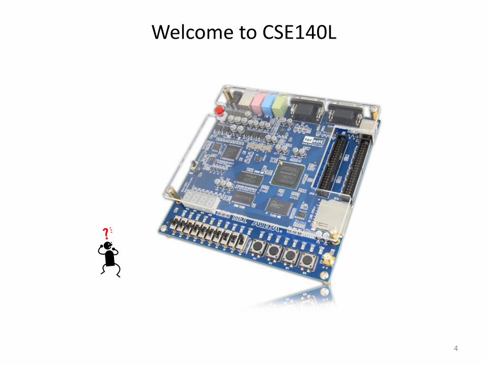
Welcome to CSE140L
4

DE1 Board Kit
5

6
FPGAs (Field Programmable Gate Arrays)
Switch Matrix
Wiring Channels
Programmable Logic Block
Switches
-SRAM based (Flash memory)
-Antifuse
Disadvantages: Penalty on area, density, speed
Advantages: Flexibility, low startup costs, low risk, revisions without changing the
hardware
Copyright © 2007 Elsevier

Homework
After installing CAD SW, study & practice the following documents and become familiar with DE1 Board operation
During your study, it will help you later if you pay close attention to I/O ports and their operation.
a) inputs, e.g., SW(Switches), KEY(PushButton), and
b) outputs, e.g., LEDG(LED green), LEDR(LED red), HEX(7-segment display).
Getting Started with Altera’s DE1 Board (Here, make sure you install a USB-Blaster
Driver properly on your PC. It should work. In case of trouble during Driver installation,
you may try this new driver.)
DE1 User Manual (Ch1,2,4 contain useful information needed for our LAB projects)
Quartus II Introduction Using Schematic Design (Here, follow the tutorial and
complete the design. Implement a light controller circuit on DE1 board by following the step-by-step
instructions described in the document.)
7

What is CAD flow?
8

9

CAD flow
• Design Entry – the desired circuit is specified either by means of a schematic diagram, or by using a hardware description language, such as Verilog or VHDL
• Synthesis – the entered design is synthesized into a circuit that consists of the logic elements (LEs) provided in the FPGA chip
• Functional Simulation – the synthesized circuit is tested to verify its functional correctness; this simulation does not take into account any timing issues
10

CAD flow
• Fitting – the CAD Fitter tool determines the placement of the LEs defined in the netlist into the LEs in an actual FPGA chip; it also chooses routing wires in the chip to make the required connections between specific LEs
• Timing Analysis – propagation delays along the various paths in the fitted circuit are analyzed to provide an indication of the expected performance of the circuit
• Timing Simulation – the fitted circuit is tested to verify both its functional correctness and timing
• Programming and Configuration – the designed circuit is implemented in a physical FPGA chip by programming the configuration switches that configure the LEs and establish the required wiring connections
11

12
Types: Behavior Description Structure Description
Languages: C, System C, Verilog, VHDL State Diagram Schematic Diagram
Register Transfer Level Description
Netlist of Logic
Physical Layout
Logic Synthesis
Placement, Routing
Mask Fabrication FPGAs
1. Design Specification: Hardware Description 2. Synthesis: Logic, Physical Layout 3. Analysis: Functional, Timing Verification
General Design Flow Algorithm Architecture

Example: Combinational circuit design flow:
Design requirements => Truth Table => (minimized) Boolean equation for each output => CAD Design flow => system on HW(FPGA, Board)
13

Combinational Logic
A B 16 different outputs
0 0 0000000011111111
0 1 0000111100001111
1 0 0011001100110011
1 1 0101010101010101
Q: What is the name of logic function for each output?
(e.g., AND, NOT, XOR, etc.)
14

Q: How to design N-way light controller?
15
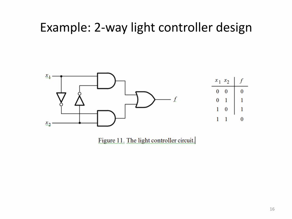
Example: 2-way light controller design
16

Combinational circuit design flow(cont'd):
Example: 2-way light controller(or N-way light controller in general) Assuming the initial condition of “the output is OFF when input x1=x2=0(=Down)”, the
design requirement is "Odd number of 1s in the input switches turns the output light ON, and even number of 1s in the input switches turns the output light OFF". => x1 x2 | f => f = (~x1 AND x2) OR (x1 AND ~x2) => QuartusCAD 0 0 | 0(=OFF) 0 1 | 1(=ON) => Sim. => Program in DE1 board => Testing 1 0 | 1 1 1 | 0 => Demo to others !
17

Timing behavior
• Real circuits have delays!
• Gate delay – time for an output of the gate to change after its input changes
• We can simulate timing delays in Quartus II to see these delays
• Tpd Specifies the maximum acceptable input to non-registered output delay,
that is,
the time required for a signal from an input pin to propagate through combinatorial logic and appear at an output pin.
18

Gate delay
• Notice rise time, fall time, and gate delay:
19
input output
input
output

Quartus II Timing Simulation
20
Notice the glitches and delay in the output

Copyright © 2007 Elsevier 21
Digital Technologies
CPU(Central Processing Unit) GPU(Graphics Processing Unit) DSP(Digital Signal Processor) SoC(System on Chip) FPGA (Field Programmable Gate Array) ASIC (Application Specific Integrated Circuit) Custom Designs etc.

Homework
• Can you implement a logic with NOT and NAND /NOR gate(s) only?
Why?
Foe example, NOT: ~A = ~(A AND A) = A NAND A, A NOR A
AND: A AND B = ~(~(A AND B)) = ~(A NAND B) ~A NOR ~B
OR: A OR B = ~(~(A OR B)) = ~A NAND ~B ~(A NOR B)
How about others? They are a combination of NOT, NAND/NOR, AND/OR.
22

Multiplexers
23
-Multiplexers (MUXes) are like selectors. There is one output, 2 or more inputs, and a “selector” input that determines which of those inputs gets outputed. -Allows several devices to share one single line.
MUX
A
B
S
Z
This is a 2:1 mux. It has 2 inputs, 1 output. Because there are only 2 inputs, S is one bit. If S=0, then we output A. If S=1, then we output B.

Multiplexers
S A B Z
0 1 1 1
0 1 0 1
0 0 1 0
0 0 0 0
1 1 1 1
1 1 0 0
1 0 1 1
1 0 0 0
24
-The truth table for the 1-bit 2:1 MUX.
When S=0, the MUX will select A as its output. It doesn’t matter what B is. Likewise, When S=1, B is selected as output.
Q: What is the boolean equation of this MUX? Z = ?????

Multiplexers
25
-If S is 0, then I0 will pass and I1 is blocked. Thus, y=I0. -Likewise, if S is 1, y=I1.