Embed Size (px)
Citation preview

VAX 6000 Model 400 System
Digital Technical Journal Digital Equipment Corporation
Volume 2 Number 2
Spring I990

Editorial J ~ n c (; Blake, lditor Rarbar;~ Lindmark, Associ:rte Editor Richard W. Hcane. Managing Editor
Cover Design Our cover depicts some of the common equutions and terminology used in vectorp~'(~'cssing, which is one of the featured topics in this issue. The vir Xr ~ c c t o r r o c e extends the VAX 6000 family to d r e s s the compuling nc,cvi.s of numerically intensiw applications. 7Be VAX 6000 h.I~~lcl~~OO systcm is a bright star in Digital S family of midrntzge mzrltipmcesson and this isszre S main product t h e m
i%e corer u~m designed by David Comberg and Karulj Zieglw of the Corporate Design Grotlp.
Circu la t ion Catherine M. Phillips. Administr:ttor Suzanne). Babineau. Secretary
P r o d u c t i o n I lclen L. P:rttcrson. Production Editor Nancy Jones, Typographer Rchccca A . Barker, Typographer I'ctcr W'oodbury, lllustraror and Design"
Advisory B o a r d Samuel H. Fuller. Chairman Robert M. Clorioso John W. hlccredie Mahendra R . Patel E <;mnt Snviers I<ohcrt K . Spitz \Vllll;~m D. Strecker Victor A . Vyssotsky
'The Oigilnl TechnicalJorrrcrl is published quarterly by Digital Equipment Corporation. 146 Main Street ML01-3lB68. Maynartl. ~ ~ s ~ t c h u s e t t s 01754-257 I. Subscriptions to theJournal a;e S.iO.00 for four issues and must he prepaid in [I.s. funds. Univer- sity and college professors and Ph.D. stutlents in the electrical engineering and computer science fields receive cornplimcn- tary subscriptions upon rcqucst. Orders, inquiries, and address changes should be sent to The I>igilul7krhrzicalJr,urnalat the published-by address Inquiric!, can also be sent electronically on NI:AHNE'I' to [email protected]. Single copies and back issues are a~ti lnhlc for S16.00 each from Digital Press of Digital Equipment Corporation, 12 Crosby Drive. Bcdl'ord, &la 01-30- 1493.
Digital ernployces may send subscription orders on the EX~T to RD\'AX::JOIlRNAL or by interoffice mail to mailstop Ml.0 I-JIB($%. Orders should include badge number, cost center, site localion code and address, and g o u p name. (1,s. engineers in Engineer- ing nnd ~anufacturingrece&e complimen~ary subscriptions; engfncrrs in [ h u e organizations in countries outside the 1i.S. shchld contact thefirnal office to receive their complimentary bubscriptions. All employees must advise of changes of addrclis.
Comments on the content of any paper are welcomed ant1 may be sent to the editor at the published-hy or network addtcjs.
Copyright 1990 Digital Equipment Corporation. Copying without fee is permitted provided that such copies are made for use in cducntional institr~tions by hculty niembers and nre not tlistributed for commercial :td\,ant;~ne. Abstractina with credit of Digit" Equipment Corporation's authorship is permitted. All rights rescrvcd.
The information in this Journal is sitbjcct to change without notice and should not be consrrued as a commitment by Digital Equipment Corporation. Digital Equipment Corporation assumes no rcsponsibiliry for any errors that may appear in this Journal.
ISSN 0898-90 1 X
Documentation Number EI'-(: 1')71i-[)P
The following are trademarks of Digital Equ~pment Corpora- tion: ( : I , DECnet, I)E(:st;ltion 3100, Dli(:\+.inclows. Digital, the Digit:tl logo, HSC, 1MicroVAX, 11%55. Thinwire. VAX, VAX-1 l/780. VAX 6000, VAX 8700, VAX 8800, \:\x 9000, \ r ~ x ~ ~ , VAXcluster, VAX FORTRAN. VAXvector6000, VYS. IILTRIX, XMI.
I l N l X is a registered trademark of American Telephone & Telegraph Company.
dbx is :I registered trademark of dbx, Inc.
hlll'h is a trademark ofhl~l's Computer S!,srcms. Inc.
Book production was done by Difiit:ll's Educational Ser\'ices Media Communications Group in Hedford, MA.

I Contents
9 Foreword Pauline A . Nist
VAX 6000 Model 400 System
1 1 Vector Processing on the VAXvector 6000 Model 400 Debra L. Slater, David M. Fenwick, D. John Shakshober, and Douglas D. Williams
27 The VAX 6000 Model 400 ScalurProcessor Module Patrick Sullivan, Michael A. Callander, Sr., James R. Lundberg, Rebecca L. Stamm, and William J. Bowhill
36 An Overview of the VAX 6000 Mo&l 400 Chip Set W. Hugh Durdan, William J . Bowhill, John F. Brown, William V. Herrick, Richard C. Marcello, Sridhar Samudrala, G. Michael Uhler, and Nicholas Wade
5 2 VM 6000 Model 400 Physical Technology John T. Bartoszek, Robert]. Hannemann, Stephen P. Hansen, Rol~ertJ. McCarty, and John C. Sweeney
64 vAX 6000 Model 400 CPU Chip Set Functional Design Verification Richard E . Calcagni and Will Sherwood
73 Test and Qualification of the VM 6000 Mo&l400 System John W. Croll, Larry T. Camilli, and Anthony J. Vaccaro
84 Development of the DECstation 3100 Thomas C . Furlong, Michael J . K . Nielsen, and Neil C. Wilhelm
89 Compiler Optimization in RISC Systems Larry R. Weber

1 Editor% Introduction
Jane C. Blake
This Spring 1990 issue marks the second issue to be published on the new quarterly schedule of the Digital TechnicalJournal. This is also the fust year that the Journal is available by subscription-a service our readers have asked for and which we are glad to be able to offer.
The Journal will continue to focus each issue on a product theme. In fact, two products are featured in this issue. The main theme is the latest addition to the VAX 6000 family, the Model 400. With its multi- processing capabilities, this midrange family of systems provides a highly configurable and expand- able computing environment. Because the same cabinet, buses, and power systems are used by all family members, systems can easily be upgraded to achieve higher levels of performance. Papers in this issue describe VAX 6000 Model 400 imo\~ations and additions, including a new vector processor and a higher performance scalar processor module, chip set design and verification, physical technology advances, and system test. The second theme com- prises two papers related to Digital's workstation development, specifically the DECstation 3100, and compiler optimization in RISC systems.
Opening this issue is a paper on one of Digital's first vector processors. Dave Fenwick, John Shakshober, Debra Slater, and Doug Williams review the design alternatives for the VAXvector GOO0 Model 400 processor and describe its function units. They then give examples of how the units combine to deliver high performance for computa- tionally intensive applications.
The Model 400 also has a new scalar processor, with nearly twice the performance of its prede- cessor, the Model 300. In their paper, Pat Sullivan, Mike Callander, Jim Lundberg, Rebecca Stamm, and
Bill Bowhill discuss the module design and give particulars on how difficult signal integrity prob- lems were resolved.
The five system chips that reside on the module are the topic of our next paper by Hugh Durdan, Bill Bowhill, John Brown, Bill Hcrrick, Rich Marccllo, Sri Samudrala, Mike Uhler, and Nick Wade. From their discussions of the chip designs, we learn how the best features of the VAX 8700 ECL-based, pipelined system and of previous VLsI designs were incorporated in the chip set, which achieves a cycle time of 28 nanoseconds.
This fast cycle time was one of several require- ments that drove a significant design effort for the physical technology. John Bartoszek, Rob Hannemann, Steve Hansen, Bob McCarty, and John Sweeney describe the technological advances achieved in a number of areas, including tape- automated bonding, semicustomized ceramic single-chip package design, and testability.
The two papers that close this collection of papers on the VAX 6000 Model 400 address chip design verification and system test. Rick Calcagni and Will Sherwood explain the engineers' multipronged approach to design verification, an approach neces- sitated by the complexity of the chip set. Then, John Croll, Larry Camilli, and Tony Vaccaro present a paper on the methods and tools designed to com- pletely test the interaction of VAX 6000 Model 400 system's hardware and softwarc.
In the last two papers, the topic turns to work- stations. Tom Furlong, Mike Nielsen, and Neil Wilhelm provide an overview of the successful project undertaken to build a fast, competitively priced, RJSC-based, ULTRIX workstation, called the DECstation 3100. The Journal is fortunate also to have a related paper on compiler optimization in MSC systems by Larry Weber, vice president, MIPS Systems, Inc. MIPS Systems built the RISC chip set incorporated in the DECstation 3100 workstation.
I thank Steve Holrnes of the Midrange Systems Business Group for his help in selecting topics on the Model 400, and Gillian Scholes of Digital and Joanne Hasegawa of MIPS Systems, Inc., for their help in obtaining the workstation and RlSC papers in this issue.

Biographies
M William J. Bowhill As a principal engineer with the Semiconductor Engineer- ing Group, William Bowhill is project leader for an engineering team that is designing an execution unit section of a large CMOS-based microprocessor. He has applied for two patents for his design work on the vector interface and backup control chip on the VAx 6000 Model 400 system. Bill also holds a patent for his work in relation to the Model 400's floating point accelerator chip. He joined Digital in 1985. Bill was educated in Great Britain and received a B.Eng. (honors) in electronic engineering from Liverpool University.
John T. Bartoszek John Bartoszek currently manages the Physical Technology Group within the SDE that is responsible for physical technology applications and product designs. John previously managed the PTG physical technology pro- gram that spawned the physical technology used on the VAX 6000 Model 400 CPU module. He joined Digital in 1981 and has a B.S. in nuclear engineering from Lowell Technological Institute. He holds two patents for thermal control devices. John has authored several papers on spacecraft thermal control, solar energy, and electronics cooling and interconnect technologies.
John F. Brown After receiving an M.S.E.E. from Cornell University in 1980, John Brown joined Digital's engineering staff. At present, he is a principal engi- neer and design team manager for the instruction decode section of the next generation CMOS-based VAX microprocessor. John's previous responsibilities include technical contributions to both the VAx 6000 Model 400 and the Model 200 chip sets. He was also the hardware engineer for the extended floating point data type enhancement to the VAX-111780 system. John currently holds one patent, has two patent applications pending, and has authored technical papers for several publications.
Richard E. Calcagni A member of the Semiconductor Engineering Group's VLSI microprocessor verification group, Richard Calcagni has contributed to the design of several VLSI microprocessors in the areas of microcode, verification, and prototype system debugging. He has published several papers on CPU design, modeling, and verification. Prior to his work with microprocessors, he worked on module test process development for Digital's Customer Services Manufacturing organization. Before joining Digital in 1979, Rick worked for Burroughs Corporation. He received a B.S. (1976) in electrical engineering from the University of Rhode Island.
Michael A. Callander, Sr. Michael Callander is a principal engineer in Digital's Semiconductor Engineering Group. At present, he is responsible for the archi- tecture of a future VAX CPU module. Mike led the VAX 6000 Model 400 system's REXMI chip set design project. His previous experience with Digital includes the design and verification of the CPU module for the VAX 8200 system and the VAX 8300 system. Mike received his B.S.E.E. degree from the University of Massachusetts in 1982. He joined Digital upon graduation.

Biographies
A Larry T. Carnilli Since joining Digital in 1979, Larry Camilli has been a member of several product clrvelopMent projects. He is currently a software engineering supervisor and project I u d a - for the architecture verification software development project, which fontsw on the development and maintenance of test &ate for mf and future architectures. Larry's previous responsi- bilities include the deyelopment of components for a microcode compiler, and a sdmare Wacs and analysis package. He holds a B.S.E.E. from Clarkson UnivfX'siQ and 14 a student in the M S C.S. degree program at Worcester Poly- technical Institute.
Joha Croll John Croll is a principal software engineer in the Midrange Systems Engineering Group. In this position, he is responsible for devefoplng systcms test tools for a fwurc hardware product. John was a team l&r in the Systems Integration Group for the VAX 6000 Model 400 system. He was also a project leader for thc ckvelopment of the VAX 6000 Model 400 console software. John joined Digital in 1978, and his previous responsibilities include the dwclopmcnt of device dr ivrrs and other system software. He received a B.S.E E. (1978) from Drexel University and is a member of IEEE and ACM.
W. Hugh Durdan A graduate of the Rensselaer Polytechnical Institute, Hugh Durdan is a consulting e m in the Semiconductor Engineering Group. In this position, his major r a p m b i l i t y is management of chip development. Hugh became involved in the VAX 6000 Model 400's chip design at its earliest begin- nings in 1984. He led the behnvioral modeling effort and the cache controller chlp design projcct. Hc ah0 managed the development of the custom chip set for theViLXvector proccsvnc and wchitected and specified the vector i n t e r k e bus. Hugh joined Digital in 1M and worked on the chip design of the VAX 8200 processor.
David M. Fenwick Tknrcbitect of the VAXvector 6000 Model 400 processor, David Fenwick joined W t a l ' s United Kingdom office in 1980 and transferred to the United States in 1983. He Is a principal engineer for the Low find Midrange Systems Group. His wvlaur experience with Digital includes field service regional support in t k Uniced Kingdom and project leadership for the DMB32 commuolurians c o n t m k far the European engineering office. He also worked on the VAXW and XIM programs in the United States. Dave received a B.Sc. fw) Ftnrn Laughborough University of Technology in England.
Thomas C. Furlong The development of Digital's RISC-based workstations is the responsibility of Engineering Manager Thomas Furlong. It was Tom's Palo Altebased design group that brought the MIPS RISC technology into Digital and developed the DECstation 3100 workstation. Tom has been with Digital for ten years. In d i r i o n to his work with RISC-based workstations, he was a member of the start-up team for the VAxstation group. Tom is originally from Detroit, ~Michlgm, 4 eamed a B.S.E E from Michigan State University. He holds two patents related to graphics workstation design and has three patents pending on the next-generation products.

--
Robert J. Hannemm Robert Hannemann is group manager of the SCIT Design and Engineering Physical Technology Group. His group is responsible for the delivery of IC packaging, module, physical design and test technology for Digital's microprocessor-based systems. A senior consultant engineer, Rob joined Digital in 1978. His prior experience includes positions at Bell Telephone Laboratories and the University of Maryland, where he was a member of the faculty. Rob holds the Sc.D. degree in mechanical engineering from MIT. He also holds two patents and has published several papers on heat transfer engineering and electronics packaging.
Stephen P. Hansen Senior Manager Stephen Hansen manages the SDEIPTG Technical Office. In this position, he coordinates programs related to cost- effective packaging for future CMOS-based products, defines technical solutions for the next generation of semiconductor packaging, and provides technical coordination for external packaging and intercomect-related activities. In his twelve years with Digital, Steve has developed several packages and assembly processes for internally manufactured CMOS products, including the tape- automated bonding process. He holds two patents in the areas of tape-automated bonding and packaging.
William V. Herrick Senior Consultant Engineer William Herrick is currently managing a new generation VAX chip design project in the Semiconductor Engineering Group. He joined Digital in 1977 and has been a member of many ZMOS- and CMOS-based product development projects, including the PDP-11/23 system and the VAX 8200 system. Before coming to Digital, Bill worked for Raytheon and GTE Sylvania. He has coauthored several papers on solid-state physics and tvIOS chip design. Bill received a B.S.E.E. (1969, magna cum laude) from Tufts University, and an S.M.E.E. (1971) and E.E. (197 1) from MIT and is a member of TAU Beta Pi, Eta Kappa Nu, and Sigma Xi.
James R. Lundberg James Lundberg joined Digital in 1985. Initially, he was a product engineer with the MOS Product Engineering Group and worked on many projects, including BIlC and CQBIC. Jim is currently a senior engineer in Digital's Semiconductor Engineering Group. He was responsible for the signal integrity on the \/AX 6000 Model 400 system and is now working on the signal integrity for an advanced CMOS CPU chip set and module. Before coming to Digital, Jim operated his own business. He is a member of Tau Beta Pi and Phi Kappa Phi. He received a B.S.E.E. (1985, honors) from the University of Illinois.
Richard C. Marcello A contributor to the design of the vAx 6000 Model 400 system, Richard Marcello is currently an engineering manager for a new- generation VAX chip design project. Rich was involved with reliability analysis of semiconductor devices before moving into design five years ago. He worked for Fairchild Semiconductor before joining Digital in 1981. Rich coauthored the paper "System, Process and Design Implications of a Reduced Supply Voltage Microprocessor," which he recently presented at the ISSCC. He received B.B.A. and B.S.E.E. (1980) degrees from the University of Notre Dame and a M.S.C.S. (1985) degree from Boston University.

Biographies
Robert J. McCarty Since joining Digital in 1982, Robert McCarty has been involved in several major product development efforts. He managed the VAX 6000 Model 400 system's physical design project and M31 console and instn~mentntion module development, and led the PDP-11/84 system engineer- ing project. Before coming to Digital, Bob worked for AM International as the project leader for a laser-based document printer that was part of a document communication system. He holds a B.S. in electrical engineering from the University of Michigan and an M.B.A. in marketing from the University of Chicago. He is a member of Tau Beta Pi and Eta Kappa Nu.
Mlchael J. K. Nielsen A consultant engineer in the Workstation Systems Englneering Group, Michael Nielsen is presently completing his responsibilities as architect and chief designer of the DECstation 5000 Model 200 workstation base platform. Mike joined Digital in 1984. Among the many projects he has worked on since that time are the DECstation 3100 workstation, for which he was the architect and chief designer, and the VAXstation 352013540, for which he was a member of the architecture and design team. Mike holds B.S.E.E., M.S.E.E. , and Ph.D.E.1. degrees from Stanford University. He is a member of Tau Beta Pi and Phi Beta Kappa.
Sridhar Samudrala Currently acting as project leader for a floating point unit, Sridhar Samudrala is a principal hardware engineer in the Semiconductor Engineering Group. Sd joined Digital in 1977. Since that time, he has worked on testing and diagnostics, as well as the VAX 8200 system microcode, and floating point architecture and design. He holds two patents for his work in floating point design. Sri has an M.Sc. (Technology) from Andhra University in India and an M.S.E.E. from the University of Wisconsin.
D. John Shakshober John Shakshober is a senior hardware engineer in the Low End Midrange Systems Group. Previously involved in the hardware design of M31, a VAX parallel processor, John is now a member of the VAx GOO0 Model 400 hardware group, where his particular focus is vector processor design. He joined Digital in 1984 after receiving a B s in computer engineering from the Rochester Institute of Technology. John received a M.S.E.E. from Carnell University in 1988. He is a member of IEEE and Tau Beta Pi. John's latest published technical paper, "Parallel Algorithms for Super Performance," was presented at Supercomputing 89.
Will Sherwood As a software consulting engineer, Will Sherwood manages the Semiconductor Engineering Group's VLSI microprocessor verification group. Previously, he managed the DECSIM logic simulation group. Will joined Digital in 1975 after receiving B.S.E.E. and M.S.E.E. degrees from Carnegie-Mellon University. In addition to his contribution to the Digital Technical Journal, he has published 15 technical papers and is a contributing author to three books. Will is a member of the IFIPS 10.2 working group on computer hardware descrip- tion languages and has sewed as publicity chairman and program committee member for several international conferences.

Debra L. Slater In her position as principal software engineer, Debra Slater leads a group that provides performance modeling and analysis support to hard- ware development teams. She and her group were integral members of the VAXvector 6000 Model 400 vector processor design team. Prior to joining Digital in 1987, Debra worked for the Montreal Engineering Company, initially as a pro- gramrnertanalyst and later as an independent consultant. She received a B.Sc. in mathematics and computer science in 1980 from Bishop's University in Quebec. In 1981, Debra received a master's degree in applied mathematics from the University of Waterloo in Ontario.
Rebecca L. Stamm Rebecca Stamm is a principal hardware engineer in the Semiconductor Engineering Group. She is currently leading the design of the backup cache, bus interface, and pin bus for a new VAX CPU chip. Rebecca was the architect of the backup cache controller chip for the VAX 6000 Model 400
5 system. She has also worked on design and verification of a RISC microprocessor. Rebecca joined Digital in 1983. She is a member of Eta Kappa Nu and IEEE, holds one patent, and has coauthored several technical papers for the ISSCC. She
'
received a B.A. (1979) in history from Swanhmore College and a B.S.E.E. (1983) from MIT.
Patrick Sullivan The project leader for the VAX 6000 Model 400 CPU module development, Patrick Sullivan is a hardware consultant engineer in Digital's Semiconductor Engineering Group. Pat is now managing a new CPU module development project. Before his work on the VAX 6000 Model 400, he led the group effort that brought MCA emitter-coupled logic (ECL) into the corporation. He is also responsible for the development of a number of Digital's main memory products and participated in the development of several 36-bit CPUs. Pat holds a patent for a memory controller interface. He received his B.S. and M.S. degrees from Northeastern University.
John C. Sweeney Currently a principal engineer, John Sweeney is working on the testability and test process development for a future Digital product. His previous experience includes being part of the test process development for the VAX 8600 and VAX 8800 systems. John was an application engineer for GENRAD before joining Digital in 1981. He has authored several papers on boundary scan and fault isolation, and has one patent pending in relation to the VAX 6000 Model 400 system's test structures. John received a B.S.E.E. (1980) from Rensselaer Poly- technical Institute and has taken graduate courses at Northeastern University.
G. Michael Uhler G. Michael Uhler is a consulting engineer in the Semi- conductor Engineering Group, where he is currently leading the architectural definition for a new CPU. As the CPU architect for the VAX 6000 Model 400 system, Mike was responsible for the CPU architecture, performance evaluation, and CPU microcode. Since joining Digital in 1978, he has also worked on the development of symmetric multiprocessing in the TOPS-10 operating system, and on the microcode and hardware development for PDP-10 CPUs. Mike received a B.S.E.E. (1975) and M.S.C.S. (1977) from the University of Arizona and is a member of IEEE, ACM, Tau Beta Pi, and Phi Kappa Phi.
Biographies
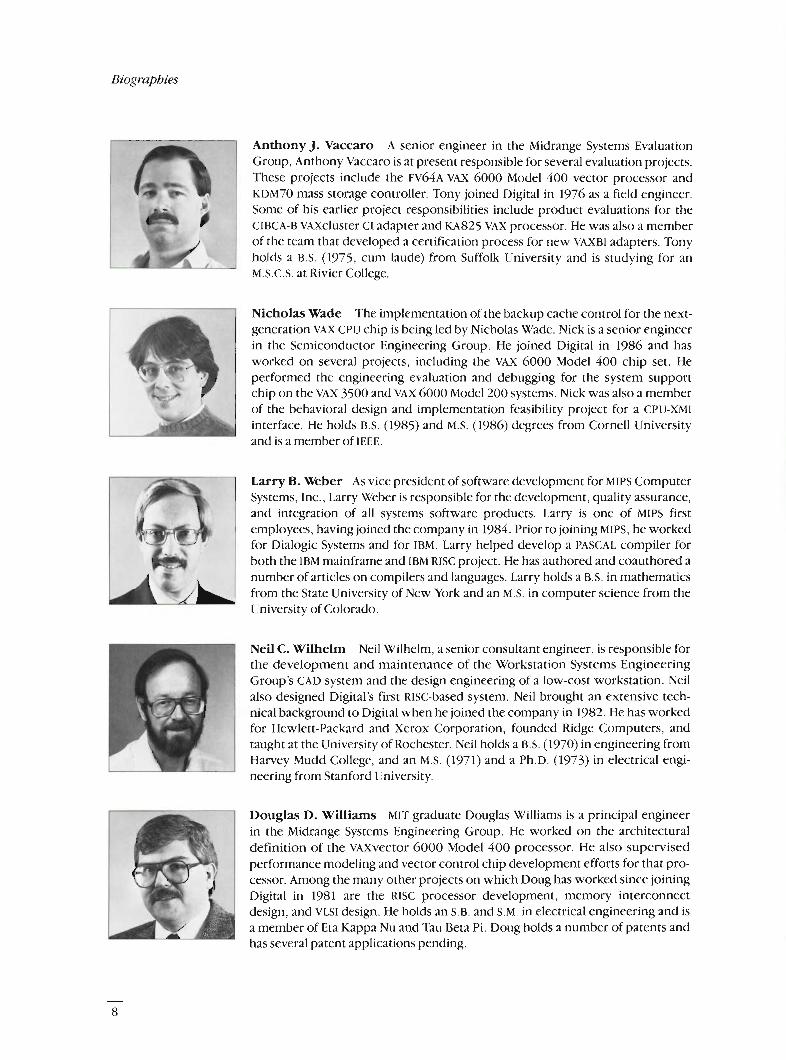
Anthony J. Vaccaro A senior engineer in the Midrange Systems Evaluation Group, Anthony Vaccaro is at present responsible for several evaluation projects. These projects include the F v ~ ~ A VAX 6000 Model 400 vector processor and KDM70 mass storage controller. Tony joined Digital in 1976 as a field engineer. Some of his earlier project responsibilities include product evaluations for the CIBCA-B VAXcluster C1 adapter and KA825 VAX processor. He was also a member of the team that developed a certification process for new VAXBI adapters. Tony holds a B.S. (1975, cum laude) from Suffolk University and is studying for an M.S.C.S. at Rivier College.
Nicholas Wade The implementation of the backup cache control for the next- generation VAX CPU chip is being led by Nicholas Wade. Nick is a senior engineer in the Semiconductor Engineering Group. He joined Digital in 1786 and has worked on several projects, including the VAX 6000 Model 400 chip set. He performed the engineering evaluation and debugging for the system support chip on the VAX 3500 and VAX 6000 Model 200 systems. Nick was also a member of the behavioral design and implementation feasibility project for a CPU-XMI interface. He holds B.S. (1985) and M.S. (1986) degrees from Cornell University and is a member of IEEE.
Larry B. Weber As vice president of software development for MIPS Computer Systems, Inc., Larry Weber is responsible for the development, quality assurance, and integration of all systems software products. Larry is one of MIPS first employees, having joined the company in 1984. Prior to joining MIPS, he worked for Dialogic Systems and for IBM. Larry helped develop a PASCAL compiler for both the IBM mainframe and IBM RISC project. He has authored and coauthored a number of articles on compilers and languages. Larry holds a B.S. in mathematics from the State University of New York and an M.S. in computer science from the University of Colorado.
Neil C. Wilhelm Neil Wilhelm, a senior consultant engineer, is responsible for the development and maintenance of the Workstation Systems Engineering Group's CAD system and the design engineering of a low-cost workstation. Neil also designed Digital's first RISC-based system. Neil brought an extensive tech- nical background to Digital when he joined the company in 1782. He has worked for Hewlett-Packard and Xerox Corporation, founded Ridge Computers, and taught at the University of Rochester. Neil holds a B.S. (1970) in engineering from Harvey Mudd College, and an M.S. (1971) and a Ph.D. (1773) in electrical engi- neering from Stanford University.
Douglas D. Williams MIT graduate Douglas Williams is a principal engineer in the Midrange Systems Engineering Group. He worked on the architectural definition of the VAXvector 6000 Model 400 processor. He also supervised performance modeling and vector control chip development efforts for that pro- cessor. Among the many other projects on which Doug has worked since joining
, 1 1 Digital in 1781 are the RISC processor development, memory interconnect design, and VLSI design. He holds an S.B. and S.M. in electrical engineering and is a member of Eta Kappa Nu and Tau Beta Pi. Doug holds a number of patents and has several patent applications pending.

I Foreword Model 300 was introduced. The Model 400 utilized this newly architected chip set to provide single- processor performance of 7 times that of the VAX-111780 system and up to 36 times the VAX-111780 system for six-processor systems. The performance of the Model 400 was over twice the single-processor performance and more than three times the multiprocessor performance of the Model 200 series, which had been announced only a short 15 months earlier.
To support such aggressive product introduction mulme A. ~ 1 s t cycles, advanced development work on the new Group Engineering Manager generation of CMOS-2 chips began in mid-1984, Midrange Sytems Business within months of the start of the CMOS-1 designs.
Actual design work began approximately a year Because microprocessor-based computer systems later. During this period, Digital made a major deci- are complex, the work to design and architect cus- sion to formally extend the VAX architecture to tom chips must be initiated long before module and incorporate full support for vector processing into systems work begins. the base instruction set for aU future VAX proces-
Looking back at recent history, Digital int1-0- sors. To provide this support, the chip designs duced the VAX 6000 family of computers in April already under way had to be modified to incorpo- 1988 with the Model 200 series, which utilized the rate the new instructions. first generation of the CMOS-based VAX micropro- The scalar chip set developed consists of five cus- cessor. The Model 200 was fabricated in Digital's tom VLSI paas. They are the cpu chip, the floating CMOS-1 (complementary oxide semicOnduc- point accelerator chip, the vectorlcache controller tor) process. A single-~rocessor Model 210 Pro- chip, the system support chip, and the clock chip. vided 2.8 times the performance of a VAX-111780 ~ h , development of the custom chips required a system. o n e to four processor configurations Pro- team of over 40 people, including logic, circuit, and vided up to a total of 11 times the performance of a layout designers, and verification engineers. ~h~ vAX-111780 system. discuss these and scalar CP" module design, standard cell interface systems in the August 1988 issue of this journal.) design, and associated verification team comprised
In January 19893 Digita1 introduced the second an additional eight engineers. Additionally, the new generation of the 6000 the 300 vector coprocessor module required three new cus- series' The 3'' increased single~rocessor tom pans, a new gate array, and a separate module performance from 2.8 to 3.8 times the VAX-111780 designeffort, system and total performance for a six-processor Since the direct shrink of die from the CMOS-1 to system to 22 times the VAX-111780 system. The
CMOS-2 process would account for only a 30 per- 30 percent increase in single-processor perfor-
cent performance increase, the processor architec- mance was made possible by a direct shrink of the
ture had to be substantially changed to achieve die from Digital's 2.0 micron CMOS-1 process to Digital's 1.5 micron CMOS-2 process. The new pro- more aggressive performance. Early in the project
cess supported a 25 percent reduction in lateral and the chip design team established a clear goal to meet
key vertical dimensions and a 78 percent improve- or exceed the performance of the VAX 8700 proces-
ment in circuit density. Together, these changes sor, which has a performance of five times that of
improved chip performance by approximately the VAX-111780 system. Some of the architectural
30 percent. changes included the following:
However, a simple shrink of the existing die did . A more pipelined architecture, specifically, a six- not permit full exploitation of the new circuit den- level pipelined engine built around three auto- sity. Newly architected and designed parts had to nomous pipes be tailored to take full advantage of the density and speed available with the CMOS-2 process. A 64-bit wide data bus with 27 separate address
The VAX 6000 Model 400 series was formally lines versus a 32-bit multiplexed dataladdress introduced in July 1989, a mere six months after the bus used for the CMOS-1 chip

Support for decode of the new VAX vector instructions and transfer of instruction operand information to the vector interface bus and onto the vector coprocessor module
A 2 kilobyte (KB) primary on-chip cache with single-cycle access supported by a 128KB off- chip secondary cache
A 16-byte instruction prefetch queue
Two quadword write buffers in the bus interface unit
Experience with the CMOS-1 chip showed that the fabrication line was capable of producing a dis- tribution of die across a performance range of 80 to 100 nanoseconds (ns). As a result, whereas all CMOS-2 new designs supported the target of a 40 ns CPU cycle time, it was an explicit goal to support devices as fast as 28 ns, should chip yields produce sufficient quantities of faster parts. The yields at 28 ns actually exceeded predictions and permitted faster parts to be used in all products produced.
First passes of all scalar CPU chips were available in April 1988. These chips could successfully boot both the VMS and LILTRIX operating systems. This success was due in large part to the aggressive use of computer-aided design (CAD) techniques. Func- tional design verification efforts alone represented 25 person-years of work on the scalar chip set. An additional 39 person-years were necessary to com- plete the scalar CPU module and the vector copro- cessor verification efforts.
The power-on of first-pass parts represented a significant accomplishment to those who worked on the chips and the module. However, much "behind the scenes" work was necessary to achieve this milestone. The success in this area represents the culmination of work across a number of disci- plines. Besides the semiconductor devices, a new 224-lead multilayer ceramic package was devel- oped. New techniques, including tape-automated bonding (TAB), were explored to attach the die to the package, and new specifications were necessary for the actual printed wire board material and board layup. Finally, new manufacturing processes were necessary to permit surface-mount assembly and test of these devices on both sides of the module.
Although initializing the operating system on the f i s t CPU modules marks a key deliverable for the chip and board designers, it is only a starting point for the systems activity that is necessary to fully test and qualify a new product prior to the start of high-
volume manufacturing. It is often difficult to under- stand the time lag between the availability of the first prototype unit running the operating system and a product that can be shipped to the customer. However, a substantial amount of work must be done between these two events. As the formal qual- ification process for new semiconductor devices begins, a parallel effort is undertaken to build a large number of early systems. These systems are used to identify any problems that may occur when the pieces of the system are assembled into configura- tions typical of those used by actual customers. Testing is divided across several aspects, including actual beta test of prototype units at customer sites, formal testing by any required government agencies (e.g., FCC, UL, VDE), systems design verification tests, and architectural testing that ensures that the new system complies with the formal VAX architec- ture standards. Once the majority of testing is in process and the required interim milestones have been met, manufacturing begins turning the assem- bled inventory into finished products to support volume availability of the system.
When a series of systems such as the VAx 6000 family has established a history in the market, it becomes increasingly important to ensure that the announcement of the latest family member coin- cides with manufacturing's ability to quickly deliver a high volume of product on a worldwide basis. If manufacturing cannot do so, a demand will have been created that cannot be filled. Revenue and sales are lost. The full payback from the many per- son-years of design, simulation, design verification, and systems test is only finally realized when vol- ume manufacturing has begun.
The papers in this issue of the journal will provide insight not only into how microprocessors and systems are designed and architected, but also into the multidisciplinary efforts necessary to bring a successful product to market. The design of one of the first VAX vector coprocessors is also reviewed. This review offers a summary of how new architec- tural issues are resolved and how design trade-offs are made.
Moving a product from advanced development to engineering, through manufacturing, and into the customer site, over a five-year period, requires the efforts of many people around the world. Although only the direct work of a small percentage of those people are represented in these papers, the credit for the success of the products goes equally to all members of the team.

Debra L. Shter David M. Fenwick
D. Jobn Sbaksbober Douglas D. Williams
Vector Processing on the VMvector 6000 Model 400
The VAXvector 6000 Model 400processor atends the VAX 6000 family of midrange CMOS-based multiprocessm to address the computing needs of numerically inten- sive applications. B e three function units of the vectorprocessor combine to f m an overall vectorpipeline that operates at speeds of up to 90 MFLOB for single-precision calculations and 45 MFLOPs for double-precision calculations. lk processor S per- formance can also be enhanced by taking advantage of overlapping and out-of order instruction execution, as well as chaining. Further, applications can be tuned to the VAXvector 6000 hardware though algmithm optimizations in areas such as equation solvers and signal processing routines to achieve optimal perfmance. Using the VAXvector 6000 Model 400 system, p~ormance increases ranging from 3 to 35 times that of the VAX 6000 Model 400 scalar system have been realid.
Vector processing has significantly evolved over the past two decades. In the late 1960s and early 1970s, it was pioneered as a way to increase scientific application computer performance over that achieved by more traditional scalar computers. However, the technology was limited to an elite few who could afford multimillion-dollar super- computer systems and who were willing to sig- nificantly re-engineer software applications.
In the early 1980s, more sophisticated vectorizing compiler technology was developed. This technology allowed users to effectively pro- gram in high-level languages, such as FORTRAN, rather than to manually vectorize using low-level assembly language. During this period, there were also significant developments in computer algorithms that were better matched to the paral- lelism available in vector hardware.
Over the past few years, a new breed of vector processor, the mini-supercomputer, has emerged. This class of machine includes many of the perfor- mance features of traditional supercomputers, but at costs more commonly associated with super- minicomputers. Because vector processing is now a mainstream style of computing that is applicable to a wide range of uses, the VAX architecture was recently extended to include vector operations. Further, the VAX product line has been expanded to include vector processing in both the VAx 6000 midrange systems family and the VAX 9000 main- frame family of systems.'
VAX Vector Processing Overview The extension of the VAX architecture to include vector processing features was done in a manner that permitted a wide range of possible implemen- tat ion~.~ The extension also allowed existing VAx processors to execute code utilizing the new vector instructions under software emulation.
The vector extensions to the VAx architecture include:
The addition of 16 vector registers, each contain- ing 64 64-bit elements
A set of loadlstore instructions used to move up to 64 elements of a vector register to and from memory
A set of vector register-to-register arithmetic and logical instructions, operating on up to 64 ele- ments at a time
A set of instructions for synchronization between scalar and vector processing subsystems
Conceptually, the implementation of vector instructions within the VAX family of processors is similar to that of floating point instructions. To implement floating point arithmetic, some systems use dedicated floating point hardware, some sys- tems use microcode, and others emulate floating point in macrocode. In vector processing, vector instructions differ from floating point instructions
Digilal TecbnicalJournal Vol. 2 No. 2, Spring 1990 11

VAX 6000 Model 400 System
in that they are designed to be executed in a semi- autonomous manner with scalar instructions. Thus, vector instn~ctions can be executed in parallel with scalar instructions or in parallel with other vector instructions. Although the scalar and xc to r units operate somewhat independently, the units arc closely coupled to ensure that memory manage- ment exceptions are precisely reported. Special operations ensurc floating point exceptions and coherence between vector and scalar memory ref- erences are synchronized.
From a vector perspective, a typical VAX vector implementation can be reduced to five basic units. The latter four units are collectively referred to as a vector processor or vector unit. The basic units are:
A scalar processor that executes scalar instruc- tions, decodes vector instructions, which may contain multiple internal function units
A vector instruction-sequencing control and reg- ister scoreboard
A vector register file
An arithmetic pipeline or pipelines that consist of one or more arithmeticllogic units
A loadlstore unit for memory references
The vector control and scoreboard logic accepts instructions and operands from the scalar processor and dispatches them to the individual function units within the processor. It also reports exceptions and interrupts to the scalar processor. Since multiple vector instructions can be executed in parallel, the unit may contain scoreboard logic to identify and manage resource conflicts between Instructions.
The vector register f ie contains the 16 vector reg- isters, each of which consists of 64 64-bit elements. The register file ha$ multiple pons that permit loads or stores to operate while operands are sent to the arithmetic pipes and results are received.
The vector arithrnetic/logic pipelines implement all the integer, logical, and floating point instruc- tions. These pipelines may be composed of separate pipelined add, multiply, and logical units. Or, they may be composed of multiple pipes that operate in parallel, with each pipe consisting of a pipelined addlmultiplyllogic unit.
The lo;~d/store unit is responsible for memory references. It generates the required virtual addresses (VA), performs translation from v~rtual to physical addresses, and loads or stores the data to or from the register files to memory. The load/
store unit controls a cache memory and contains a virtual-to-physical address translation buffer (TR). Depending on the design of the scalar and vcctor units, there are two ways to implement the design memory interface for the scalar and vector processors:
A combined scalar and vector processor that shares a common cache, address translation logic, and path to memory subsystem
Separate scalar and vector units with separate caches and address translation buffers
Both of these approaches have their relative merits and disadvantages. When significant data- sharing between scalar and vector units exists, the combined approach provides more favorable cache performance because the common cache is updated on both scalar and vector references. Separate caches may result in additional cache misses as data is "sloshed" between scalar and vector caches. For limited data-sharing instances, the separate approach may offer more favorable cache perfor- mance. In a combined cache, vector references can displace needed scalar data and vice versa. This problem does not arise with separate caches because the scalar and vector data each has a dedicated cache. The separate cache approach also allows scalar and vector cache operations to occur in parallel.
In implementing a vector processor, the selection between the above alternatives is often driven more by technology constraints than issues of archi- tectural elegance. The VAX 9000 system, which is implemented in emitter-coupled logic (ECL), chose the combined approach. This approach supported sharing costly cache RAMS and a common path to memory. The VAXvector 6000, which is imple- mented in complementary metal oxide semi- conductor (CMOS) technology, chose the separate approach for two reasons. First, module space and package pin count constraints made it difficult to implement both scalar and vector functions on a single module. Second, the cost penalties for sepa- rate scalar and vector cache RAMS and separate paths to memory were not prohibitive.
VAX GOO0 Vector Processor Description
System Block Diagram The system block diagram for a vector-capable VAX 6000 Model 400 machine is shown in Figure 1.
12 VoI. 2 No. 2, Sprr'ng 1990 Digital TecbnicalJournal

Vector Processing on the VAXvector 6000 Model 400
I SCALAR H VECTOR PROCESSOR PROCESSOR
SCALAR I PROCESSOR H VECTOR PROCESSOR I
I I XMI SYSTEM BUS
32MB 1 "' I M E M O R Y I ... PORT CONTROL
(UP TO 256MB OR 8 MODULES) - ETHERNET + BI PORT
RAXX DISKS
SOLID- STATE DISK
Figure I VAXvecttor GOO0 Model 400 System Block Diagram with Dual Scalar and Vector Processors
The vector processor occupies a slot adjacent to the scalar processor, and both are interconnected by a short interface cable. The vector processor receives all instructions from and returns status to the scalar processor across this cable. For memory references, the vector processor has its own independent path to main memory. The VAX 6000 Model 400 system supports configurations of up to six scalar proces- sors. However, vector systems have additional configuration constraints because of the increased memory bandwidth and XMI slot requirements of the scalarlvector processor. The VAXvector 6000 Model 400 system supports configurations of single or dual scalarlvector processors, or configurations of one scalarlvector processor and up to three addi- tional scalar processors. To satisfy memory band- width requirements, VAXvector 6000 systems with a single scalar/vector processor require at least two memory controllers. Dual scalar/\~ector systems or single scalarlvector systems with additional scalar processors require at least four memory controllers.
VAX 6000 ~odel400 Vector Processor The block diagram for the vector processor is shown in Figure 2. The machine is divided into three separate function units that can operate in combination or independently:
A vector controller, implemented as a single chip
Arithmetic pipelines implemented by four pairs of chips, i.e., register file and vector data path
A loadlstore unit, implemented by one chip, which also controls a 1 megabyte (MB) cache
Vector Control Chzp When the scalar processor encounters a vector opcode, it parses and fetches the operands. The opcode and all its operands are dispatched through the instruction bus to the vector processor. For arithmetic instructions, the scalar processor will proceed to decode the next opcode in the instruction stream. However, for load and store instructions, the scalar processor is stalled until all address translations are completed. Stalling guaran- tees that any memory management violations are synchronous and that the scalar processor can restart the faulting instruction correctly. Within the vector unit the vector control chip is responsible for all scalar vector communication. When instruc- tions are received by the vector controller chip, the vector controller buffers the instructions and controls instructions issuing to the other function units within the vector processor.
An important aspect of the vector control chip is the register scoreboard logic, which identifies potential register conflicts when vector instructions are executed in parallel. By maintaining accurate register usage data, the vector control chip can optimize parallelism with the vector processor. Optimal performance is achieved by executing arithmetic operations in parallel with load and store operations, chaining the results of arithmetic opera-
Digital TecbnicalJournal Vo1. 2 No. 2. Sping 1990

VAX 6000 Model 400 System
SCALAR PROCESSOR VECTOR PROCESSOR A ,.
I \ I \
SCALAR XMI INTERFACE
CABLE
DUPLICATE H LOAi/SLORE I TAG XMI INTERFACE
1 M B VECTOR REGISTER
- DATA CACHE
FILES
XMI SYSTEM BUS
ARITHMETIC PIPELINES
Figure 2 VAXvector 6000 Model 400 Scalar/Vector Processor Block Diagram
f
tions into store operations, and even dynamically re-ordering the execution of arithmetic instructions relative to load and store instructions to improve parallelism.
The vector control chip sends all error status and machine checks to the scalar processor. When an error is encountered, the control chip attempts to retry the failing transaction. If the retry is suc- cessful, a soft error interrupt is sent to the scalar processor. If the retry fails, either a hard error interrupt or a machine check is sent to the scalar processor. Read operations that fail result in machine checks. Write operations that fail result in hard error interrupts.
Although not part of the overall control function, the vector control chip also contains logic to imple- ment the IOTA instruction. The IOTA instruction builds a set of offsets in a vector register. This func- tion did not fit conveniently in any other vector function. The control chip was selected because it had the space available to contain the function.
Vector Register File and Arithmetic Pipeline The VAXvector 6000 processor's arithmetic pipe- line is organized as four pipes. Each pipe consists of a quarter of the register file (every fourth element of the vector registers), and an associated arithmetic1 logic unit. Each individual pipeline can retire one single-precision calculation every cycle or one
double-precision calculation every two cycles. The four pipes collectively retire four single-precision calculations every cycle, or two double-precision calculations every cycle. Thus, a much higher float- ing point performance is achieved than with only one individual pipeline.
The register file chips receive instructions from the vector controller and data from the cache or loadlstore unit. The register file chip provides read operands to the arithmetic pipeline and stores write results and mask information. To maximize the use of cache bus bandwidth, two 32-bit operands can be combined into a single 64-bit transfer that is simultaneously read or written to two separate reg- ister file chips. The register file internally has four 64-bit ports. (One is a readlwrite port for memory data; two are read ports for operands; and one is a write port for results. While one instruction is writing its results, a second can start reading its operands. Thus, the instruction pipeline delay is hidden. Variations in pipeline length between instructions are smoothly handled to ensure that no gaps exist in the flow of write data.
The register file can hold two outstanding arith- metic instructions in its internal queue. Therefore, the vector controller can preload the arithmetic instruction queue with a second instruction, i.e., deferred instruction. Preloading allows the vector controller to free the cache data bus, which is also used for instruction issuance, for use by a sub-
14 Vo1.2 No. 2, Spring 1990 Dfgilal TechfcalJournal

Vector Processing on the VHXvector 6000 Model 400
sequent load or store instruction. This feature improves performance because the arithmetic pipeline can execute two arithmetic instructions in the time it takes to execute one load or store instruction.
The register file's operand and result ports are used by the vector arithmetic pipeline chip. Operand data is sent over a 32-bit bus that is driven twice per cycle. Results are returned on a separate 32-bit bus that is driven once per cycle. The two operands for single-precision instructions can be passed in one cycle, while double-precision operands take two cycles to transfer. Each arith- metic pipeline chip has a throughput of one single- precision operation per cycle, one double-precision operation per 2 cycles, and one single-precision or double-precision divide per 10 or 22 cycles. The arithmetic chip has a pipeline delay of six cycles for double-precision multiplications, and five for all others (except divides), including the data transfer cycles. Integer operations are recoded internally as double-precision floating point data types. The vector arithmetic pipeline chip is a full custom implementation largely based on the design of the scalar processor's floating point unit.'
Load/Store Unit The control chip uses the vector processor's inter- nal bus to issue instructions to the function units. However, once a load or store instruction is issued, the loadlstore chip becomes bus master and con- trols the internal bus. Either the loadlstore chip, vector register files, or the cache can drive the bus. Once a load or store instruction starts execution, no further instructions can be issued until it com- pletes. This rule simplifies the control chip score- boarding because once a load or store instruction is started, no further instnictions can start. Therefore, scoreboarding of these instructions against the out- standing load or store instruction is not necessary. Because scoreboarding of outstanding instructions requires considerable logic complexity in the vector control chip, it was important to keep the complexity of this operation minimal. An addi- tional benefit was the simplification of the internal bus protocol. It was excessively complex to imple- ment the capability to stop load or store instruc- tions in progress. This alternative was not pursued because the resulting performance benefit was minor in comparison to the amount of work involved.
The loadlstore chip executes the vector load, store, scatter and gather memory reference instruc-
tions. These instructions involve virtual-to-physical address translation, cache management, and inter- action with the memory bus. If a load or store instruction requires an offset register, such as scatter or gather, the offset register is first read into a buffer and then added to the instruction's base address. This process eliminates turning around the internal bus for each offset read, which would add more overhead. For strided load or store instruc- tions, the address is generated by adding the stride to the instruction's base address.
Load or store instructions can operate on either 32-bit (i.e., long word, single-precision) or 64-bit (i.e., quadword, double-precision) data types. When executing unity-stride 32-bit load or store instructions, the loadlstore chip operates on two elements at a time. Two 32-bit elements are com- bined into a single 64-bit cache reference. This combination significantly enhances performance enhancement in unity stride single-precision data operations.
Virtual-to-physical address translation is per- formed using an on-chip, 136-entry, 68-way-asso- ciative translation buffer (TB). This configuration maximizes address translation efficiency, which is very important because only limited chip space was available. To optimally service TB miss conditions, the loadlstore chip contains dedicated logic that directly references page table entries upon a TB miss. A simpler alternative would have been to use microcode in the scalar processor to fetch new page table entries upon a TR miss. However, the dedicated logic approach was chosen to enhance performance for applications that exceed the size of the TB. Under certain TB miss conditions, the vector processor may be unable to compute a new virtual-to-physical address translation. This situa- tion can occur when the addressed page is invalid or has been paged-out to disk. When such a miss occurs, the vector unit reports an exception back to the scalar processor. Once the scalar processor corrects the situation, the instruction is retried from the beginning.
Since the scalar processor must be able to restart the faulting vector instruction, it is important to precisely identify any vector memory management exception with the associated vector load or store instruction. This identification is achieved by block- ing issuance of further instructions until the vector unit notifies the scalar processor that the vector instruction is free of memory management faults. The vector unit contains memory management prediction logic, called MMOK logic. MMOK logic
Digital TecbnicalJournal Vo1. 2 N O , Spring 1990

VAX 6000 Model 400 System
allows the scalar processor to issue additional instructions in parallel with the execution of the vector load or store instruction. During execution of a strided vector load or store instruction, once it is established that the current vector element references the same TB entry as the last element of the load or store instruction, and that the associ- ated TB entry is free of memory-management exception conditions, the load/store unit can safely report "address translation successful," i.e., MMOK, to the scalar processor. Early prediction of success- ful address translation permits the scalar processor to be released and allows it to operate asyn- chronously with the remainder of the vector load or store instruction.
Once a physical address is obtained, the load1 store chip references its 3213 entry tag store. The address is delayed and passed to the 1MB cache data store. This delay permits cache tag lookup and com- pare to complete before data is written to the cache on store operations. In parallel, the corresponding register file address is presented to the four register file chips. The data and addresses are automatically aligned for load and store operations to permit correct reading and writing of the register file and cache data KAMs. Upon cache miss, the load/store unit queues the associated 32-byte block read oper- ation with the memory interface logic and contin- ues processing other elements. Up to four cache misses can be outstanding before the read data for the first miss returns. Hits continue to be processed while the misses are outstanding. On vector proces- sors, the most important factor is the time required to complete the entire load or store operation, rather than the time needed to fetch an individdal element. The cache miss handling feature permits the vector processor to maximize its use of available XMI bandwidth.
The vector cache tag and data are parity-pro- tected. Should a cache parity error occur, the cache is disabled and the instruction retried from the beginning. This method was the simplest option for soft recovery of cache parity errors. The operating system receives a soft error interrupt and can, at its option, re-enable the cache.
The loadlstore chip contains a 32-element write buffer to enhance performance of store operations. Since the vector cache operates at higher band- widths than the system bus, the buffer isolates the store performance from the slower XMI memory bus. Furthermore, a subsequent load instruction that hits in cache can execute while the write buffer
is being written to memory. If the load instruction takes a cache miss, the load stalls until the store completes. This simple scheme improves instruc- tion overlap when load instructions follow store instructions without adding undue complexity to the loadlstore unit design.
Performance Characteristics The interaction between the different functional units of the vector processor creates a number of sit- uations that affect the performance and execution of vector instructions. These include:
Overlapping instructions
Out-of-order instructions
Chaining
Overlap of Instructions Arithmetic and loadlstore instruction execution may overlap because the functional units are inde- pendent. In order to achieve this overlap, the following conditions must be met.
The arithmetic instruction must be issued before the load or store instruction.
There must be no register conflict between the arithmetic and loadlstore instructions.
In the following examples of arithmetic and load1 store instruction interactions, an "I" represents instruction issue time, and an " E " represents instruction execution time. The "VR" represent vector registers. The expression "std" is used to represent the stride. A series of periods ". . ." repre- sents wait time in the arithmetic unit for deferred instructions. (Note: These examples are not intended as timing diagrams.)
VVADDx VRl,VR2,VR3 IEEEEEEEE
VLDx A,std,VRl IEEEEEEEEEEEEEE
As can be seen in the example above, the execu- tion of the vector load instruction (VLDx) can overlap the vector add instruction (VVADDx) because there are no register conflicts between the two instructions. In the next example, instruction overlap is inhibited because the WADDx instruc- tion is writing to the register to be loaded, V R 3 .
VVADDx VRl,VR2,VR3 IEEEEEEEE
VLDx A,std,VR3 IEEEEEEEEEEEEEE
In comparing these two examples, it is clear that the overlap of the execution of the VVADDX and the
16 Vol. 2 No. 2, Spring 1990 Digital TecbnicalJoumal

Vector Processing on the VAXuector 6000 Mod1 400
VLDx greatly reduces the total execution time of the instruction sequence. By taking advantage of this hardware feature, application codes can show greatly improved performance.
Out-of order Instruction Execution The arithmetic unit includes a deferred instruction queue of length 1. This queue allows the vector control and scoreboard logic to queue one instruc- tion to the arithmetic unit while that unit is still executing a previous instn~ction. The vector con- troller checks the queue's status for an instruction when it checks the function unit's availability. Both the deferred and currently executing instructions are checked for register availability. This queue frees the issue unit to process another instruction rather than waiting for the arithmetic unit to com- plete its current instruction.
For the following instruction sequence,
VVADDx V R l , V R 2 , V R 3
VVMULx V R 3 , V R l , V R 4
VLDx A , s t d , V R 2
execution without a deferred instruction queue would resemble this example:
I s s u e VVADDx IEEEEEEEE
I s s u e VVMULx I EEEEEEEE
I s s u e VLDx IEEEEEEEEEEEEEE
Execution with a deferred instruction queue would look like the following:
I s s u e VVADDx I EEEEEEEE
l s s u e d e f e r r e d VVMULx I . . . . . . . E E E E E E E E
I s s u e VLDx IEEEEEEEEEEEEEE
These examples illustrate the use of a deferred arithmetic instruction. If a deferred instruction queue was not implemented, the VVnlULx instruc- tion could not be issued until the VVADDx was either completed or nearly completed. The VLDx instruction would not issue until after the W U L x was issued and would complete much later than
in the deferred instruction case. Once the VLDx instruction is issued, no other instructions may be issued. The instruction overlap execution made possible by the deferred instruction queue signi- ficantly reduces total execution time.
Comparing the last two examples, in the case where a deferred instruction queue was used, the VLDx instruction can begin executing before the WMULx. It also could complete before the VmlULx instruction completes simply because the WMULx instruction is sent to the deferred arithmetic instruction queue. This out-of-order execution of instructions allows increased overlap of instruc- tions, which again reduces the total execution time of the instruction sequence.
Chaining Vector operands are generally read from and writ- ten to the vector register file. An exception to this process occurs when a store instruction is waiting for the results of a currently executing arithmetic instruction. (Divide instructions are not included in this exception because they do not have the same degree of pipelining as the other instructions.) As results are generated by the arithmetic instruction and are ready to be written to the register file, they are also in~mediately available for input to the wait- ing store instruction. Therefore, the store instruc- tion can begin processing the data before the arithmetic instruction has completed. This process is called "chain into store." The store instruction will not overrun the arithmetic instruction because the store instruction can process data faster than the arithmetic unit can generate results.
The following instruction sequence
VVADDx VRl ,VRE,VRB
VVMULx VRl ,VRP,VR4
VSTx V R 3 , A , s t d
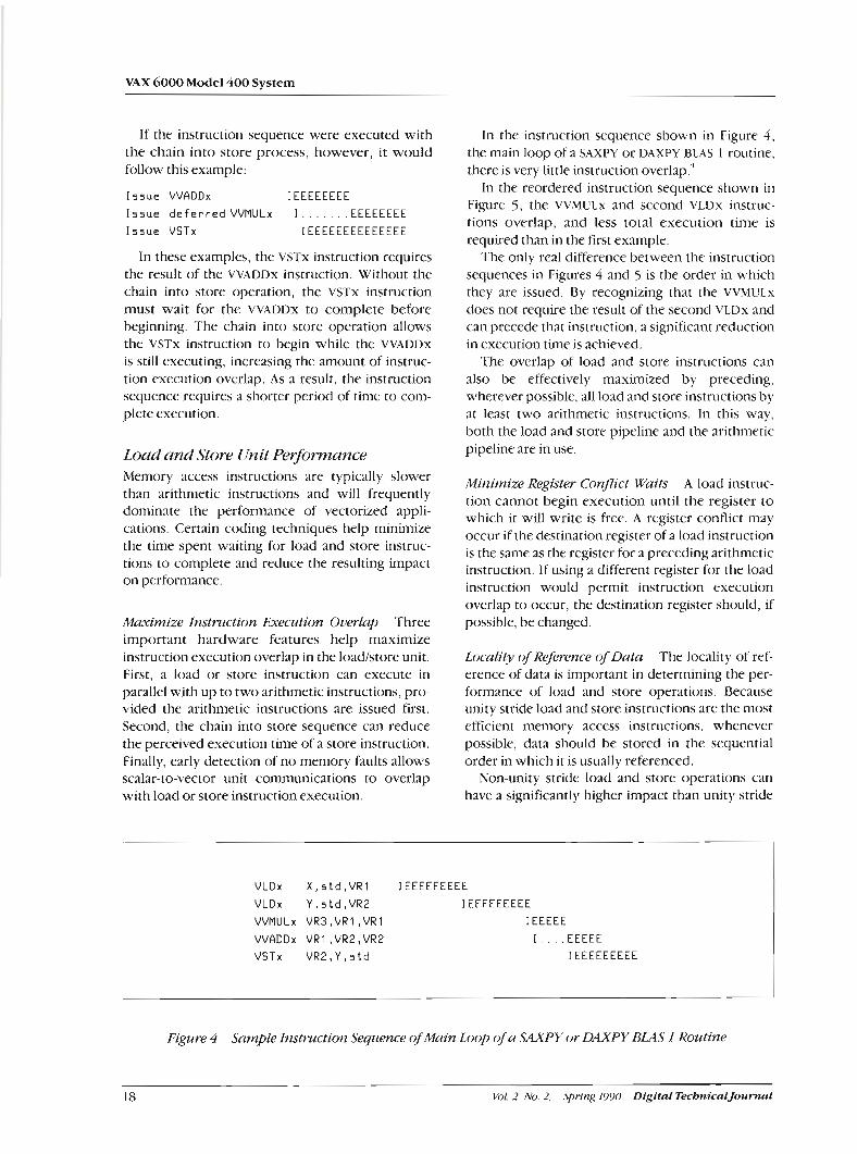
would resemble the example in Figure 3 if executed without the chain into store process.
I s s u e VVADDx [ EEEEEEEE
I s s u e d e f e r r e d VVMULx I . . . . . . . E E E E E E E E
I s s u e VSTx IEEEEEEEEEEEEEE
Figure 3 Sample lmtruction Sequence without Chain into Store
Digital TecbnlcalJournal Vol. 2 No. 2. Spring 1990 17
VAX 6000 Model 400 System
If the instruction sequence were executed with the chain into store process, however, it would follow this example:
I s s u e VVADDx I EEEEEEEE
I s s u e d e f e r r e d VVMULx I . . . . . . . E E E E E E E E
I s s u e VSTx IEEEEEEEEEEEEEE
In these examples, the VSTx instruction requires the result of the VVADDx instruction. Without the chain into store operation, the VSTx instruction must wait for the VVADDx to complete before beginning. The chain into store operation allows the VSTx instruction to begin while the VVADDx is still executing, increasing the amount of instruc- tion execution overlap. As a result, the instruction sequence requires a shorter period of time to com- plete execution.
Load and Store Unit Performance Memory access instructions are typically slower than arithmetic instructions and will frequently dominate the performance of vectorized appli- cations. Certain coding techniques help minimize the time spent waiting for load and store instruc- tions to complete and reduce the resulting impact on performance.
Maximize fnstruction Execution Ovwlap Three important hardware features help maximize instruction execution overlap in the loadtstore unit. First, a load or store instruction can execute in parallel with up to two arithmetic instructions, pro- vided the arithmetic instructions are issued first. Second, the chain into store sequence can reduce the perceived execution time of a store instruction. Finally, early detection of no memory faults allows scalar-to-vector unit communications to overlap with load or store instruction execution.
In the instruction sequence shown in Figure 4 , the main loop of a SAXPY or DAXPY BLAS 1 routine, there is very little instruction overlap.'
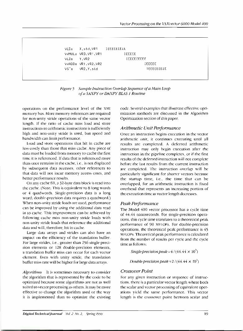
In the reordered instruction sequence shown in Figure 5, the WMULx and second VLDx instruc- tions overlap, and less total execution time is required than in the first example.
The only real difference between the instruction sequences in Figures 4 and 5 is the order in which they are issued. By recogni~ing that the VVMULX does not require the result of the second VLDx and can precede that instruction, a significant reduction in execution time is achieved.
The overlap of load and store instructions can also be effectively maximized by preceding, wherever possible, all load and store instructions by at least two arithmetic instructions. In this way, both the load and store pipeline and the arithmetic pipeline are in use.
Minimize Register Conflict Waits A load instruc- tion cannot begin execution until the register to which it will write is free. A register conflict may occur if the destination register of a load instruction is the same as the register for a preceding arithmetic instruction. I f using a different register for the load instruction would permit instruction execution overlap to occur, the destination register should, d possible, be changed.
Locality of Reference of Data The locality of ref- erence of data is important in determining the per- formance of load and store operations. Because unity stride load and store instructions are the most efficient memory access instructions, whenever possible, data should be stored in the sequential order in which it is usually referenced.
Non-unity stride load and store operations can have a significantly higher impact than unity stride
VLDx X , s t d , V R l IEEEEEEEEE
V L D x Y, s t d ,VR2 IEEEEEEEEE
VVMULx V R 3 , V R I , V R l I EEEEE
VVADDx V R l , V R 2 , V R 2 I . . . . E E E E E V S T x V R 2 , Y , s t d IEEEEEEEEE
Figure 4 Sample Instruction Sequence of Main Loop of a SAXPY or DAXPY BLAS I Routine
18 Vol. 2 No. 2. Spring 1990 Digital TecbnicalJoumal
Vector Processing on the VAXvector GOO Model 400
V L D x X , s t d , V R I IEEEEEEEEE
VVMULx V R 3 , V R I , V R l I EEEEE
V L D x Y ,VR2 IEEEEEEEEE
VVADDx V R l , V R 2 , V R 2 I EEEEE
V S T x V R 2 , Y , s t d IEEEEEEEEE
Figure 5 Sample Instruction Overlap Sequence of a Main Loop of a SAXPY or DAXPY BLAS I Routine
operations on the performance level of the XMI memory bus. More memory references are required for non-unity stride operations of the same vector length. If the ratio of cache miss load and store instructions to arithmetic instructions is sufficiently high and non-unity stride is used, bus speed and bandwidth can limit performance
Load and store operations that hit in cache are less costly than those that miss cache. Any piece of data must be loaded from memory to cache the first time it is referenced. If data that is referenced more than once remains in the cache, i e., is not displaced by subsequent data accesses, other references to that data will not incur memory access costs, and better performance results.
On any cache fill, a 32-byte data block is read into the cache. (Note: This is equivalent to 8 long words or 4 quadwords. Single-precision data is a long word; double-precision data requires a quadword.)
code. Several examples that illustrate effective opti- mization methods are discussed in the Algorithm Optimization section of this paper.
Arithmetic Unit P e r f o m n c e Once an instruction begins execution in the vector arithmetic unit, it continues executing until all results are completed. A deferred arithmetic instruction may only begin execution after the instruction in the pipeline completes, or if the first results of the deferred instruction will not complete before the last results from the current instruction are completed. The instruction overlap will be particularly significant for shorter vectors because the startup time, i.e., the time that can be overlapped, for an arithmetic instruction is fmed overhead that represents an increasing portion of the execution time as vector length decreases.
When non-unity stride loads are used, performance Peak Perfomzance can be improved by using the additional data read in to cache. This improvement can be achieved by following cache miss non-unity stride loads with non-unity stride loads that reference the additional data and will, therefore, hit in cache.
Large data arrays and strides can also have an impact on the efficiency of the translation buffer. For large strides, i.e., greater than 256 single-preci- sion elements or 128 double-precision elements, a translation buffer miss can occur for each vector element. Even with unity stride, the translation buffer miss rate will be higher for large data arrays.
Algorithm It is sometimes necessary to consider the algorithm that b represented by the code to be optimized because some algorithms are not as well suited to vector processing as others. It may be more effective to change the algorithm used or the way it is implemented than to optimize the existing
The Model 4 0 0 vector processor has a cycle time of 44.44 nanoseconds. For single-precision opera- tions, this cycle time translates to a theoretical peak performance of 9 0 MFLOPs. For double-precision operations, the theoretical peak performance is 45 MFLOPs. Theoretical peak performance is calculated from the number of results per cycle and the cycle time as follows:
Single-precision peak =4 / (44.44 x 10")
Double-precisionpeak =2 / (44.44 x 10')
Crossover Point For any given instruction or sequence of instruc- tions, there is a particular vector length where both the scalar and vector processing of equivalent oper- ations yield the same performance. This vector length is the crossover point between scalar and
Digital TecbnicalJournal V i f . 2 No. 2, Spring 1990

VAX 6000 Model 400 System
vector processing and is unique to the particular instruction or sequence. Scalar operations are faster for vector lengths below the crossover point. Vector operations are more efficient for vector lengths above the crossover point. A low crossover point is considered a benefit because it indicates that it is easier to take advantage of the power of the vector processor. A low crossover point means that more code can benefit from the vector processor.
For any single, isolated vector instruction, the crossover point on the Model 400 system is quite Low, generally about 3 or 4. However, an instruction is not performed in isolation. In a routine or application, other factors affect the performance of the operations on short vectors. These effects are particularly seen when the short vector's data is used in several vector operations.
On the Model 400 system, performing as much code as possible on the vector processor, including short vector length sections, can mean higher system performance. Performance is improved because thc cache is used more optimally. Speci- fically, once vector instructions have referenced a piece of data, that data is included in the vector unit's cache. Subsequent scalar operations on that data will require moving the data from the vector cache into the scalar cache. Continued code sec- tions of vector references followed by scalar references tend to invalidate the two caches too frequently. Therefore, a vector operation is usually more efficient than a scalar operation. The cross- over point on the Model 400 system is low enough that scalar processing is the faster alternative only for isolated operations on short vectors.
Algorith Optimization Examples The previous section of this paper discussed how the characteristics of the VAXvector 4000 Model 400 system's vector processor can affect performance. The following examples illustrate how that perfor- mance information can be used to build optimized routines. The examples also show how an algorithm and its implementation can change the performance of an application on the vector 6000 processor.
Algorithm changes can alter the data access pat- terns to use the memorj7 subsystcm more efficiently, can increase the average vector length, and can min- imize the number of vector operations required. By applying Amdahl's Law of vectorization, we can improve performance by increasing the percentage of code that is vectorized.
To take advantage of the processing power of the VAxvector 6000 Model 400 system, we concen- trated on four basic optimization methods:
Rearrange code for maximum vectorization of the inner loop and remove data dependencies within the loop
Vectorize across contiguous memory locations to produce unity stride vectors for increased cache hit rates and opti.mized cache miss handling
Reuse the data already loaded into the vector reg- isters as frequently as possible to reduce the number of vector load and store operations
Maximize instnlction execution overlap by pair- ing arithmetic instructions between load and store instructions wherever possible
(Note: Further information on optimization techniques in FOR'TRAN can be found in the VAX FORTRAN Performance Guide available with the FORTRAN-High Performance tion on.^ Additional information on macrocoding for the vavec tor 6000 Model 400 vector processor can be found in the VAX 6000 Vector Processor ProgrammerS Guide. ")
By analyzing the groups of applications that have high vector processing potential, we identified two basic arras where optimization techniques can be most useful: equation solvers and signal process- ing routines. For example, computational fluid dynamics, finite element analysis, molecular dynamics, c i rc~~i t simulation, quantum chromody- namics, and economic modeling applications use various types of simultaneous or differential equa- tion solvers. Applications such as air pollution modeling, seismic analysis, weather forecasting, radar imaging, speech and image processing, and many other scientific and engineering applications use signal processing routines, such as fast Fourier transforms, to obtain solutions.
Equation Solvers Equation solvers generally fall into four categories: general rectangle, symmetric, hermitian, and tri- diagonal. The most common benchmark used to measure a computer system's ability to solve a general rectangular system of linear equations is ~ i n ~ a c k . ' The Linpack benchmarks, developed at Argonne National I.aboratory, measure the perfor- mance across different computer systems while solving dense systems of 100, 300, and 1000 linear equations.
VoL I No. 2, Sl~ring 1990 Digital TechnicalJournal

Vector Processing on the VHXvector 6000 iModel400
These benchmarks are currently written to call subroutines from the Linpack library. The subrou- tines, in turn, call the basic linear algebra subrou- tines (BLAS) at the lowest level. For each benchmark size, there are different optimization rules which govern the type ofchanges permitted in the Linpack report. Optimizations to the RLAS routines are always allowed. Modifications can be made to the FORTRAN source or by supplying the routine in macrocode. Algorithm changes are only allowed for the largest problem size, the solution to a system of 1000 linear equations.
The smallest problem size uses a two-dimensional array that is 100 by 100. The benchmarks are writ- ten to use Gaussian elimination for solving 100 simultaneous equations. This two-step method fea- tures a factorization routine, x(;EFA, and a solver, xGESL. Both are column-oriented algorithms and use vector-vector level I BLAS routines. Column orientation increases program efficiency because it improves locality of data based o n the way FORTRAN stores arrays.
As shown in Figure 6, the B1.AS level 1 routines allow the user to schedule the instructions opti- mally in vector macrocode. Deficiencies in BLAS 1 routines include frequent synchronization, a large calling overhead, and more vector load and store operations in comparison to other vector arithmetic operations.
The performance of the Linpack 100 by 100 benchmark. which calls the Figure 3 routine, shows how an algorithm with approximately 80 percent vectorization can be limited by the scalar portion. One form of Amdahl's I,aw relates the percentage of vectorized code compared to the percentage of scalar code to define an overall vector speedup. This ratio between scalar runtime and vector runtime is described by the following formula:
Vector speedup = time scalar 1 (% lscular l x time scalar) + ([ % uector 1 x time wctor)
Under Amdahl's Law, the maximum vector speedup possible, assuming an infinitely fast vector processor, is:
Vector speedup = 1.0 / (0.2) x 1 .O + (0.8) x 0 = 1.0/0.2 = 5.0
As shown in Figure 7, the Model 400 processor achieves a vector speedup of approximately 3 for the 100 by 100 Linpack benchmark when using the BLAS 1 subroutines. It follows Amdahl's Law closely because it is small enough to fit the vector proces- sor's 1 Mbyte cache and, therefore, incurs very little overhead due to memory hierarchy.
For the Linpack 300 by 300 benchmark, opti- mizations include the use of routines that are equivalent to matrix-vector level 2 BLAS routines.
xAXPY - compute5 Y (1 ) = Y ( 1 ) + a X ( 1 )
where x = p r e c ~ s l o n = F , D, G
MSYNC
LOOP:
;synchronize w l t h s c a l a r
VLDx X ( I ) , s t d , V R O
VSMULx a,VRO,VRO
VLDx Y ( I ) , s t d , V R I
VVADDx VRO,VRI,VRI
VSTx V R l , Y ( I ) , s t d
I NC I
I F ( I < S I Z ) GOT0 LOOP
MSYNC
; X ( I ) 15 l o a d e d I n t o VRO
;VRO g e t s t h e p r o d u c t o f VRO
;and t h e s c a l a r v a l u e " a "
; Y ( I ) g e t l o a d e d i n t o VR1
;VR1 g e t s VRO summed w i t h VR1
;VR1 15 s t o r e d back I n t o Y ( 1 )
; ~ n c r e m e n t I by v e c t o r l e n g t h
; Loop f o r a l l v a l u e s o f I
;synchronize w i t h s c a l a r
Figure 6 Core Loop ofla BLAS I Routine Using Vector- Vector Operations
Digital TecbnicalJournal Vol 2 IVO. 2, .S/)rirlg 1990 2 1

VAX 6000 Model 400 System
DIMENSION OF PROBLEM SIZE
Figure 7 Linpnck Pwfornmnce Graph, Doubleprecision BLAS Algorithms
Figure 8 details the core loop of a BLAS 2 routine. BLAS 2 routines make better use of cache and trans- lation buffers than the Bl.As 1 routines do. Also, HLAS 2 routines have a better ratio between vector arithmetics and vector load and stores. The larger matrix size increases the average vector length. Per- formance is improved by amortizing the time to decode instructions across a larger work load.
By removing one vector load and one vcctor store from the innermo4t loop, the BLAS 2 routine has a better ratio of arithmetic operations to load and
store operations than HLAS 1 routincs. Although the 300 by 300 array fits into the vect~)r processor's 1 MB cache, not all the cache can be mapped by its translation buffer. By changing the sequence in which this routine is called in the program, the data access patterns can bc altered to better use the vector unit's translation buffer. Thus, higher per- formance is obtained.
The percent of vectorization increases primarily because of tlie increase in the matrix size from 100 by 100 to 300 by 300. With a vector fraction of approximately 95 percent, Figure 7 shows the speedup improvement in the 300 by 300 bench- mark when using methods based on HI.AS 2 rou- tines. With a matrix vector algorithm, the 300 by 300 benchmark yields speedups of between 1 0 and 12 over its scalar counterpart.
There are no set rules to follow when solving the largest problem size, a set of 1000 simultaneous equations. One potential tool for optimizing this benchmark is tlie LAPACK library developed by Argonne National Laboratory, in conjunction with the Ilniversity of Illinois Center for Supercomputing Research and Development (<:SRD). The LAPACK
library features equation solving algorithms that will block the data array into sections that fit into
xGEMV - computes Y(1) = Y(1) + X ( J ) * N ( I ,J)
where x = p r e c i s i o n = F, D, G
MSYNC ;synchron ize w i t h s c a l a r
I LOOP:
VLDx Y( I ) ,s td ,VRO ; Y ( I ) i s loaded as VRO
JLOOP.
VLDx M ( I , J ) , s t d , V R I ;VRI g e t s columns o f M ( I , J )
VSMULx X(J),VRI,VR2 ;VR2 g e t s t h e p r o d u c t o f VRl
;and X(J) as a s c a l a r
VVADDx VRO,VR2,VRO ;VRO g e t s VRO summed w i t h VR2
I NC J I F ( J < S I Z ) GOT0 JLOOP ;Loop f o r a l l v a l u e s o f J
VSTx VRO,Y( I ) ,5 td ;VRO g e t s s t o r e d i n t o Y ( I )
I NC
I F ( I < SIZ) GOT0 ILOOP ;Loop f o r a l l v a l u e s o f 1
MSYNC ;synchron ize w l t h s c a l a r
Figure 8 Core Loop of a BLAS 2 Routine Using Matrix-Vector Operations
2 2 Vol. 2 NO. 2, Spring 1990 Digital TecbnicalJournal

Vector Processing on the VAXuector 6000 Model 400
a given cache size. The LAPACK library calls not only the BLAS 1 and BLAS 2 routines but also a third level of BLAS, called matrix-matrix BLAS or the BLAS
level 3: Figure 9 shows that a matrix-matrix multiply is at
the heart of one BLAS 3 routine. The matrix multi- plication computation can be blocked for modern architectures with cache memories. Highly efficient vectorized matrix multiplication routines have been written for the VAX vector architecture. For example, a double precision 64 by 64 matrix multiplication achieves over 85 percent of the peak MFLOl's on the Model 400 system.
Performance can be further improved with other methods that increase the reuse of data while it is contained in the vector registers. For example, loop unrolling can be done until all the vector registers have been fi~lly utilized. Partial results can be formed within the innermost loop to minimize the loads and stores required. Because both rows and columns are traversed, the algorithm can be blocked for cache size. The VAXvector Model 400 system
exhibits vector speedups greater than 35 for the 64 by 64 matrix multiplication described above.
Although the overall performance of the 1000 by 1000 size benchmark is less than a single 64 by 64 matrix multiplication, it does indicate the potential performance when blocking is used. Improving the performance of this benchmark is most challenging because the 1000 by 1000 matrix requires about eight times the vector cache size of I M B . Further analysis is being conducted to determine the most efficient block size that would maximize the use of BLAS 3 and remain within the size of the cache for a given block of code.
The vectorized fraction increases to approxi- mately 98 percent for the 1000 by 1000 benchmark. The proportion of vector arithmetics relative to vector loads and stores is much improved for the BLAS 3s. Although the cache is exceeded, perfor- mance more than doubles when using a method that can block data based on the BLAS 3 algorithms. Therefore, the ITAXvector 6000 Model 400 pro- cessor's performance for Linpack 1000 by 1000
xGEMM - computes Y ( I , J ) = Y ( I , J ) + X ( I , K ) * M ( K , J )
where x = p r e c ~ s ~ o n = F , D , G
MSYNC
I JLOOP :
VLDx
KLOOP:
VLDx M ( K , J ) , s t d , V R l
VSMULx X ( I , K ) , V R I , V R l
VVADDx VRO,VR2,VRO
I NC K
I F (K < 51 2 ) GOT0 KLOOP
RESET K
VSTx V R O , Y ( I , J ) , s t d
I NC I
I F ( I < 512 ) GOT0 IJLOOP
I NC J
RESET I
I F ( J < 512 ) GOT0 IJLOOP
MSYNC
; s y n c h r o n i z e w ~ t h s c a l a r
; Y ( l : N , J ) g e t s l o a d e d I n t o VRO
; K ( 1 :N ,K ) g e t l o a d e d I n t o VRl
;VRl g e t s VR1 summed w i t h
; X ( I ,K) as a s c a l a r
;VRO g e t s VRO summed w ~ t h VR2
; I n c r e m e n t K by v e c t o r l e n g t h
; r e s e t I t o S I Z
;VRO g e t s s t o r e d i n t o Y ( I , J )
; i n c r e m e n t I b y v e c t o r l e n g t h
; I n c r e m e n t J b y v e c t o r l e n g t h
; r e s e t I t o S I Z
;synchronize w ~ t h s c a l a r
Figure 9 Core Loop of a BLAS 3 Routine Using Mat*-Matrix Operations
Digital TechniculJoumal Vol 2 No 2, Spring 1990 23

VAX 6000 Model 400 System
obtained a vector speedup of approximately 25, as BIT shown in Figure 7. REVERSAL
REORDER CORRECT RESULT
Signal ~ e s s ~ ' ~ g - Fast Fouriev T r a m f m The Fourier tramsfom decomposes a waveform, or more generally, a collection of data, into com- ponent sine and cosine representation. The discrete Fourier transform (Dm) of a data set of length .V
performs the transformation following the strict mathematical definition which requires o(iv2) floating point operations. In 1965, the fast Fowicr transform (FFT) was developed by Cooley and Tukey. FFT reduced the number of operations to O(N x L O G I N ] ) , which is a significant improve- ment for computational speed.'
As shown in Figure 10, the complex data in the bottom butterfly is multiplied in each stage by the appropriate weight. The result is then added to the top butterfly and subtr~cted Eron~ the bottom butterfly. If t k algrr(t1im is left in this configura- tion, it must use non-unity stride vectors, very short vectors, or masked arithmetic operations to per- form the ver). sm:~ll butterflies.
Optimized One-dimensional Fast Fourier Transforms The bit-reversal process that permutes the data to a form that enables the Coolcy-Tukey algorithm to work is also shown in Figure 10. When using vectors, a common approach to performing the bit- reversal reordering is to use vector gather or vector
9 scatter instructions. These instructions allow vector loads and stores to be performed using an index register. Vector loads and stores require a con- stant stride. Holvever, vector g;rthcr and scatter operations allow the user to build a vector of offsets t o support indirect addressing in vector mode. Both gather ancl scatter instructions are available with VAX vectors.
A vector implementation of the I:I:T algorithm has been developed that is well suited for the \'AX \,ector :rrchitecture. One optimization made to the algo- rithm involves moving the bit-reversal section of the code t o a place where the data permutation will benefit vector processing. By doing so, two goals are accomplished. First, the slower vector gather operations are moved to the center of the algorithm such that the data will alrcady be in the vector cache. In Figure 1 0 , the first FFI'stage starts out with large butterfly distances. After each stage the butter- fly tlistancc is hal\.cd. For the optirnizcd \usion
LOG (N) STAGE 1 STAGE 2 STAGE 3 STAGE 4 STAGES
Figure I 0 The Coolcy-Tdcy Ruttc'1"ji!!~ Crupb, One-dimensional Fast Fourier Trun.Fform for N = 16)
shown in Figure 11, the bit-reversal permutation is performed as close to the center as possible, when the stage number = LOG(N)I2. To complete the algorithm, the butterfly distances now increase again. Second, this process entirely eliminates the need for short butterflies.
Another optimization made to the FF'I' algorithm is the use of a table lookup method to access the sine and cosine P~ctors, which recluccs repetitive calls to the computationally intensive trigonometric filnc- tions. The initialization of this trigonon~etric table has been fully vectorized but shows only a modest factor of 2 performance gain. To build the table, a first-order linear recurrence loop is formed that severely limits vector speedup. Because this calcula- tion is only done once, it becomes negligible for multiple calls to the one-dimensional I:~:'l's and for all higher dimensional FF1's. The benchmark shown in Figure 12 was looped and includes thc calculation of the trigonometric table performed once for each FFT data length.
Reusing data in the vector registers also saves vector processing time. The VAX vector architecture provides 16 vector registers. If all 16 registers are used carefully, data can be reused by two successive butterfly stages without storing and reloatling the data. With half the number of loads and stores, the vector performance almost doubles.
24 Vol. 2 IVO. 2. S/)rit~g I990 Digital TecbnicalJournal

Vector Processing on the VMi~ector 6000 Model 400
BIT R E V E R S A L REORDER
STAGE 1 STAGE 2 (HAS
CORRECT RESULT
STAGE 3 STAGE 4
R E G - R E U S E )
Figure I 1 Optimized Coolty-Tz~key Butterfly Graplj, One-dimensional Fast Fourier Transforin for N = I6
Optimized Two-dimensional Fast Fourier Transforms The optimized one-dimensional FFT can be used to compute multidimensional FFTs. Figure 13 shows how an N by N two-dimensional FFT can be com- puted by performing N one-dimensional column FFTs and then N one-dimensional row FFTs. The same routine can be called for column or row access FFTs by simply varying the stride parameter that is passed to the routine. (Note: In FORTRAN, the column access is unity stride and the row access has a stride of the dimension of the array.)
For improved performance on VAX vector systems, the use of a matrix transpose can dra- matically increase the vector processing perfor- mance of two-dimensional FFTs for large values of N, i.e., N > 256. The difference between unity stride and non-unity stridc is the key performance issue. Figure 14 shows that a vectorized matrix transpose can be performed after each set of N one-dirnen- sional FPTs. The computation will be equivalent to F i g ~ ~ r e 10 b ~ ~ t with a matrix transpose: each one- dimensional FFT will be column access which is unity stride. The overhead of transposing the matrix becomes negligible for large values of N.
When thc value of N is relatively small, i.e., N < 256, the two-dimensional FFT can be com- puted by calling a one-dimensional FFT of length N'.
Dfgflal TecbnicalJournal Vol. 2 No. 2, Spring I990
I I
0 1000 2000 3000 4000 5000 LENGTH OF DATA SIZE
KEY: r WITH REG-REUSE
0 NO REG-REUSE
Figure 12 One-dimensional Fast Fourier Transform Performance Graph, Optimized Single-precision Cmnplex Transfom
The small two-dimensional FFT can achieve per- formance equal to that of the aggregate size one- dimensional FFT by linearizing the data array. Figure 15 shows the trade-off between using the lin- earized two-dimensional routine (for small N ) and the transposed method (for large N ) to maintain high performance across all data sizes.
The optimization of an algorithm that vectorizes poorly in its original form has been shown. The resulting algorithm yields much higher perfor- mance on the VAXvector 6000 Model 400 processor. High performance is due to the unique way the algorithm touches contiguous memory locations and its effort to maximize the vector length. The implementation described above always uses unity stride vectors and always results in a vector length of 64 for FFT lengths greater than 2 K ( 2 X 1024).
N 1-D FFTS N 1-D FFTS
C O L U M N ROW
Figure 1.3 Two-dimensional Fast Fourier Transforms Using N Column and N Row One-dimensionul Fast Fourier Transforms

VAX 6000 Model 400 System
N 1 - D FFTS TRANSPOSE
COLUMN
N 1-D FFTS
COLUMN
TRANSPOSE
Figure 14 Two-dimensional Fust Fout-ier Transforms Using a /Matrix Transpose between Each Set of N Column One-dimensional Fast Fourier Transfotm
Linear algebra and signal processing applications that utilize the various hardware features have demonstrated vector speedups between 3 and 35 over the scalar VAX 6000 Model 400 CPL! times. With the integrated vector processing available on the VAXvector 6000 Model 400, the performance of computationally intensive applications may now approach that of supercomputers.
Acknowledgments The authors would like to acknowledge the tech- nical contribution of the following people: Paul Brodeur, Doi~g Burns, Giao Dau, Bob Dickson, Darrel Donaldson, Hugh Durdan, Bill Gist, Anil Jain, Chandrika Kamath, Dwight Manley, Mike Pline, John Redford, Sean Reilly, Tim Stanley, and Mike Uhler.
References
1. J. Croll, "VAX 6000 Model 400 Multiprocessor System Overview," Proceedings of COMPCON '90 (IEEE, forthcoming 1990).
2. D. Bhandarkar and R. Brunner, "Vector Exten- sions to the VAX Architecture," Proceedings of COMPCON '90 (IEEE, forthcoming 1990).
3. M . (;avrielov et a]. "A 50 MHz Uniformly Pipe- lined Floating-Point Arithmetic Processor," Proceedings of ISSCC '89 (IEEE, February 1989): 50-5 1.
4. J. Dongarra, Perfcn-nmnce of Various Computers Using Standard Linear Equations SoJware in a FORTRAN Enz~ironmmzt, (Argome, 1L: Argonne National Laboratory, June 1989).
I 0 200 400 600 800 1000 1200
5. VAX FORTRAN Per@-t?zalzce Guide (Maynard:
DIMENSION OF PROBLEM SIZE Digital Equipment Corporation, Order No. K F Y .
PLA-PB75A-TE, forthcoming 1990). . .- .
A TRANSPOSED
LINEARIZED
Figure 15 Two-dimensional Fast Fourier Transform Perfomnce Graph, Optimized Single-precision Cmplex TransJorm-
6. VAX 6000 bkctor Processor Programmer? Guide mayna nard: Digital Equipment Corporation, Order No. EK6OVPLA-I-'(;, forthcoming 1990).
7. C. Bischof et al., LAPACK, (Argonne, I L : Argonne National Laboratory, April 1989).
8. J. Cooley and J . Tukey, "An Algorithm for Machine Calculation of Complex Fourier Series," Mathematical Computing, no. 19 ( 1965): 297-301.
Summary 9. P. Swartztrauber, "Vectorizing the FFT's," Parallel Computing (Academic Press, 1982):
The VAXvector 6000 Model 400 processor delivers 51-85.
high performance for computationally intensive apilic~tions. The CMOS-based VAXvector 6000 is capable of operating at peak speeds of 90 ,\IFLOPS single precision and 45 MFLOPs double precision.
1/01. 2 No. 2, .S/)rin~ 090 Digital TechnicalJoumal

Patrick Sullivan Michael A. Callander, Sr.
James R. Lundberg Rebecca L. Stamm WilliamJ. Bowbill
The VAX 6000 Model 400 Scalar Processor Module
The VAY 6000 filodel 400 CPIJ module is the latest generation of the crnzpatible VAX 6000 family of computers. me Model 400 is a single-board, CI~IOS-based CPII that signficantly extends the pwformance of the VRu 6000 series. The system provides nearly 7 VAX units ~Jperformance (V1JP.s) in single-processm applications and up to -36 VilPs in six-processor systems. The Model 400 module is a plug-in r e p l a c m t for the Model 200 and ~~(Iodel300p~ocess~s. Chip set and module designers ofthis new system cooperated closely to meet aggressive timing andperfmzance goals. Several enhancements were made to the cache and bus intwface units to improve multipro- cessorperfmnce. A vector intwface was included for connection to a companion oecturprocessor module. Signal integrity was an important consideration for both chip and module design.
When the Midrange Systems Business (MSB) Group began to develop the \,Ax 6000 series, the Semi- conductor Engineering Group (SEC;) had started development of a new CMOS-based cPu chip set.' The project's goals were the following:
Achieve (;PO performance at least equal to the 5.5 VlIPs of the VAX 8700 system
Support a 28-nanosecond (ns) module cycle time
At that time, the VAX 8700 system was the fastest VAX available and used emitter-coupled logic (ECL) to achieve a 45-ns cycle time. SEG designers believed a system implemented in CMOS technology could meet or exceed that performance level and at a much lower manufacturing cost. With reference to the second goal. a 28-11s cycle time would take advantage of chip sets that could run faster than the projected 40 11s cycle time.
In discussions with MSB, we realized our module project could be modified to include an XMI inter- face and, therefore, become another member of the VAX 6000 series.' We then agreed to undertake a joint development effort between MSB and SEG, which resulted in the VAX 6000 Model 400 scalar CPU. Development of this scalar processor module is the focus of this paper.
Halfway through the project, support for a vector processor module was included because the VAX architecture was extended to include vector
Digital TecbnicalJournal Vo1. 2 No. 2, Spring 1990
instructions. The vector processor module, which was developed by MSB, can provide a significant performance boost for certain classes of vector problems.
The first Model 400 systems were shipped in July 1989. This delivery was made just 15 months after the introduction of the initial 6000 Model 200 series.
Design Challenges The aggressive 28-11s cycle time goal for the module design required a tight coupling of the chip set and module design efforts. With this short 28-11s cycle time goal, the module interconnect had to be treated as transmission lines. Consequently, signal integrity considerations were critical to design suc- cess and would impact all areas of the design- chip, package, and etch board. The approach taken to address signal integrity is described in more detail in the Signal Integrity section.
The performance goals also dictated a change in the VAX 6000 Model 400 data and address line (DAL) pin bus. The older, less complex multiplexed 32-bit bus would have to be separated into a separate 27-bit address bus (A-bus) and a 64-bit data bus (D-bus). That decision in turn resulted in the need for high pin count packages (224 pins) and the asso- ciated signal integrity challenges of dealing with as many as 90 output drivers switching simulta-

VAX 6000 Model 400 System
neousl!., while driving transmission lines with a low effective impedance of 60 ohms.
Two new technologies were needed to meet these challenges. First, new chip packages had to be developed to supply the increased number of signal pins. The packages use multilayer ceramic sub- strates to provide signal planes, as well as separate power and ground planes for both intern:~l logic and pad ring power. The packages have 224 pins on a 25-mil pitch and are surface mounted for better
controller chip (VC), a clock distribution chip (CLK), and a system support chip (RSSC). The REXMl interface consists of three chips: two copies of the data path chip (XDP), and a controllerlinterface chip (XCA).
A block diagram of the XRP module is shown in Figure 1. The module consists of four major sections:
CPlJ and F-chip floating point accelerator
module routability. Second, the 25-mil package pin rn VC chip and backup cache RAM array pitch required the use of a finer geometry etch
The Rssc: system support chip board: 13-mil module vias and 10-mil routing pitch. This specification required the ph!,sic:~l design team rn The Xkll interface, including REXMI
to initiate a very close development ;uid qual- ification effort with the etch hoard vendors.'
Major Module Subsections The Model 400 n~odulc, or XHI', is a single-board VAX CI'U implemcntccl with the Model -i00 chip set and a REXMl interface to the X M l bus.' The chip set includes five chips: a CPU chip (RliXSLO), a floating point accelerator chip (F-chip), a backup cache
The RliX520 is the first VAX microprocessor chip to implement a fully pipelined microarchitecture. The F-chip has (5-bit-wide data paths and a pipe- lined execution unit. These chips cooperate to implement the base instruction group of the VAX
architecture. The two chips represent the CPU sec- tion of the XRI' module, and both chips connect directly to the DAL. Both chips also have a private 8-bit bus for control and status information.
VECTOR INTERFACE XCI BUS (CABLE)
- REX520 CPU WITH CACHE
DATA
< XMI . >
DAL
SYSTEM AND AUXILIARY CONSOLE
U
Figure 1 XRP Module Block Diagrunz
'ONTRoL RSSC
I
Vol 2 /\lo 2, .S/)rir?g 1990 Digital TecbnicalJournal
F.CHIP
CLOCK
BACKUP CACHE RAMS
ADDRESS
DATA ROM AND EEPROM
I I
CONTROL VC
I-BUS REXMl

f i e VAX 6000 model 400 Scubr Processor Module
The REX520 provides the hardware and microcode necessary to parse specifiers, execute instructions, handle exceptions, and otherwise implernent the VAX architecture. The REX520 ;ilso provides hill vAx memory management, a 4-gigabyte (GB) virtual address space, and support for 512 megabytes (Me) of physical memory. The chip contains a (%entry, fi~lly associative transla- tion buffer. Both process and system-space map- pings are stored in the buffer. The chip also includes a 2-kilobyte (KB), direct-mapped instruction and data cache Cprimary cache) with an 8-byte block ancl fill size.
The F-chip enhances the computation phase of floating point and certain integer instructions in conjunction with the REX520 chip. The F-chip exe- cutes the F-, I ) - , and (;-format floating point instruc- tions, as well as the long word variants of integer multiply. The chip receives operands from the REX520, computes the result, and passes the result ancl status back to the REX520. The REX520 chip completes the instruction.
?'he \'C chip implements a 2K tag store and neces- sary control for a 128KR backup cache. The cache uses 15-ns, 16~-by-4 static random-access mem- ories (SIUMs) on the module. The vC chip also includes a copy o f the primary cache tag store, the invalidate bus (I-bus), and an interface to the vector interface bus (VIB). The I-bus connects to the REXMI and boosts performance by doing invalidate filter- ing. The cache design is discussed in more detail in the Model 400 Caches section.
The RSSC chip is a modification of the SSC chip used in a number of previous Cpus. It incorporates the common core of h~nctions that support the chip set in the xbll system environment. TheRSSC chip is discussed in detail in the Model 400 System Support Chip section.
The XMI interface consists of the standard XMI- comer components and the REXMl chip set. The H E X M I chip set interfaces the DAL to the xC1, which is the user side of the XMl comer. The XiMI interface is discussed further in the XMlr Interface and REXM[ section.
1)AL operations are synchronous on the XRP module. Therefore, a very low skew clock distri- bution system was required. The clock chip and controlled, equal-length clock lines to each of the chips provide this distribution. The clock chip receives a 143-megahertz (hlHz) oscillator input and provides two sets of synchronous four-phase clocks. Each clock phase driver output can drive four 50-ohm lines in parallel. In the XRP design,
there are eight chips that require all four phases, and each set of clock outputs drives four chip loads. Discrete Schottky diodes are used at the receiving ends of all the clock lines for termination. This design achieved a clock skew of less than 0.5 ns at the receiving chips.
The DAL pin bus is a fully synchronous, hand- shake protocol bus. The DAL is nonpended in that it Ins only one transaction outstanding at a time, and it is also nonrnultiplexed with separate address and data lines. The design consists of a 27-bit address bus (A-bus), a 64-bit data bus (D-bus), and associated control signals. The DAL runs at a 28-ns cycle time, synchronous with the Model 400 chip set. The tim- ing is controlled by 4 overlapping 14-ns-wide clock phases, which are separated from each other by 7 ns. The ['-chip, F-chip, VC chip, backup cache RAMS, and the REXMl communicate through the DAL. The P-chip is the default bus master and contains the arbiter for the bus. The P-chip uses the DAL to initiate reads and writes to the backup cache and main memory through the KEXMI. The backup cache and the REXlLlI send read data to the P-chip.
The bus master notifies other bus nodes of the start of a transaction. The receiving node can termi- nate a transaction in one of three ways. I t can indicate a successful completion, indicate an error, or request that the transaction be retried. Once the receiver indicates one of the transaction termina- tion signals, the bus master deactivates.
One DAL transaction takes a minimum of three cycles. The maximum transaction time depends upon the system response to read and write requests. The RSSC includes a bus timeout mecha- nism that prevents the system from hanging. Most DAL signals are transferred in three phases, although some control signals are transferred in two.
As noted earlier, vector interface capability was added after the \'Ax architecture was extended to support vector operations. The vector h~nctionality was added to the vC chip because that chip could accommodate the extra pins required for the inter- face, i.e., 224 pins versus 1 6 4 .
'The major units of the X R P module are described in the following sections.
Model 400 Caches The XRP module incorporates a two-level cache hierarchy that maximizes <:PU performance. The first-level cache is the primary cache, called the P-cache, which is contained entirely in the P-chip. The second-level is the backup cachc or H-cache,

VAX 6000 Model 400 System
:~nd it consists of the VC chip and 24 15-ns, 16~-by-4 static R:\>ls. Thc VC chip contains the tag store and the control logic for the B-cache. The SRAMs store thc cache data. The P-cache and the 6-cache contain both instructions and data.
The 1'-cache is a 2KB cache and is direct-mapped, with an 8-byte block size. The cache is read- allocate, no-write-allocate, and write-through. In write-through, writes that hit in the cache are simultaneously written to the cache and to main memory. The P-cache can perform a new access once every cycle.
Each P-cache tag entry includes an 18bit tag, one valid bit, and one parity bit. There arc 256 tags cor- responding to 256 data blocks. Each data block con- tains 8 data bytes and 8 parity bits, with parity was implemented on each byte. Parity permits a byte write to be done without the need to recalculate parity across the other bytes. This process avoids the performance penalty that occurs whcn all bytes arc not written at once, as in the read-modify-write process.
The B-cache is a 128KB cache and is direct- mapped, with an 8-byte access size. I t has a 16-byte sub-block size and a 64-byte block size. The cache is also rc;id-allocate, no-write-allocate, and write- through. Thcre are 2048 entries in the B-cache tag store. Each entry contains a 12-bit tag, 4 valid bits, and a parity bit.
Backup Cache Hit Designers optimized access time to the backup cache by connecting the cache RAMS dircctly to the DAL. The chips, the bus, and the specialized hit sig- nals are shown in Figure 2.
When the P-chip issues a read on the DAL, it drives the address on the A-bus to the VC chip and cache RAMS. The P-chip asserts memory read (MI:hLRD-L). The VC chip uses MEM-RD-L to enable the assertion of the cache RAM chip select lines (BC-C'S-I.< 7:0 > ). This process accomplishes two things. 'I'he chip select lines are valid by the time the P-chip has driven the A-bus to a valid state. Further, the total time to perform the rrad from the RAMS is minimized.
The RAM access begins in parallel with the tag store access. If the vC chip finds a match in the tag store, it asserts BC-HIT-L to notify the P-chip. By the time BC-HI.1'-L is asserted, the data from the cache RAMS is valid on the D-bus, and the P-chip then accepts the data.
If the VC chip does not find a match in the tag store, it asserts BC-MISS-L. This signal notifies the
Figure2 Backup Cache Access Di~rgrnln
R E X M I to send the read request to memory. A t thc same time, the VC chip asserts the cache KAM write enable (BC-WE-L) and waits for the data to return from memory. When the REXMI returns the data, it asserts a transaction termination signal. This signal informs the P-chip, the VC chip, and the F-chip that data is rcady on the bus. All three chips receive the data simultaneously, and the data is written into the cache RAMS. The transaction ends when the P-chip accepts the data.
XMIlnterface and REXMI The XRP module accesses all memory ancl 110 devices over the XMI bus. Thc REXMl interfaces the chip set to the XMI bus by means of two data path chips (XDPs) and one controlladdress chip (XCA). Each XDP is responsible for 32 bits of the REXMI's 64-bit data path. The XCA is responsible for the address data path, DAL control logic, X M [ control logic, and control of the two XDPs. Both chips are implemented in CMOS-2 standard cells.
The primary tasks of the XMI interface are to
Forward REX520 references to the XMl
Implement a write buffer that reduces traffic to main memory
Support control of cache fills and cache invalidates
Support XMl interrupt logic
W'ol. 2 IVO. 2. Spring I990 Digital TecbnicalJournal

m e VAX 6000 Model 400 Scalar Processor ililodule
CMOS-2 Standard Cell Technology Custom chips were not used to implement the XCA and X D P chips. Instead, two alternatives were investigated. These alternatives were to ube either gate arrays or standard cells from external vendors, or internally built CMOS-2 standard cells
A number of external vendors offered products with the density and internal gate speeds needed to implement the REXMI chips. However, none offered the performance and flexibility needed to interface to the DAI.. Therefore, we chose the CMOS-2 stan- dard cells, which could Interface to the DAL
We added a number of new cells to the standard cell library: several versions of a high-performance 3.3-volt output driver, input latch with the required 0-ns set-up time, and a low skew internal clock buffer capable of driving over 30 picofarads of capacitance. These new cells were largely based on circuits designed for the custom CMOS-2 CPU chips, whlch met the high performance goals set by the Model 400 program.
Per-jomnce Considerations Performance bottlenecks in high-speed computer systems most often occur in the path to and from main memory. The XRP's two cache levels greatly reduce the number of reads required. However, since both caches are write-through, all writes must be forwarded to main memory by the REXMI. To improve performance, the REXMI implements a write buffer with four octaword (16-byte) entries.
The write buffer improves performance in two ways. First, it decouples the R E X 5 2 0 write rate from the slower XMI write rate. The R E X 5 2 0 can transfer 8 bytes of write data to the REXMI every three cycles. This data is loaded into the write buffer and later transferred to main memory at XMI speeds.
Second, the write buffer combines multiple REX520 writes into a single XMI write. The most efficient write transaction is a full octaword write. The REXMI always tries to combine multiple R E X 5 2 0 writes into full octaword writes. The REXMI loads write data into a write buffer entry. The write data is held until either a new octaword address is received or a purge write buffer condi- tion occurs. When the REXMI receives a write to a new octaword address, the current write buffer entry is marked full. A new write buffer entry is then opened with the new octaword address. Write buffer entries are transmitted as they are marked full. To guarantee that the write buffer data is writ- ten to main memory in a timely manner, the write buffer is flushed before the following conditions:
XMI r/O space read or write
Interlock read or unlock write
Interprocessor interlock
XMI read to an octaword location that includes data contained in the write buffer
In response to a clear write buffer command
Combining P-chip writes reduces the number of write transactions needed by over 40 percent. This reduction certainly improves single-processor per- formance. However, the greatest improvement is in n~ultiprocessor performance where the XMI band- width required by each Cl'u is reduced.
Cache Coherence The XRP module allows data to be shared among multiple processors. The XRP design assures that the most recently written copy of any data is pro- vided to a running process. This process is called cache coherence.
In multiprocessing systems, coherence can be ensured in two ways. Cached copies of data that have been written can be invalidated, or each cache can be updated with more recent data. Since it is simpler to invalidate than to update, an invalidation scheme was implemented on the X R P module.
Every X R P processor write is sent to XMI mem- ory. When an XRI' module broadcasts a write on the XMI, the command, address, and data are captured in memory. Other XRI' modules capture the com- mand and address to invalidate any valid B-cache or P-cache entries that correspond to the address.
We could have opted to broadcast all x M 1 writes as invalidates on the DAL. However, this method would have greatly increased the DAL traffic and would have reduced the processor's performance. To increase the performance of multiprocessor systems, the V C chip provides a low-overhead invalidate mechanism through the 1-bus. The REXMI can determine through the I-bus if data is currently cached. The REXMI sends an invalidate on the DAL only if the data is cached.
The v C chip maintains a duplicate copy of the primary cache tag store. The chip accesses the copy in parallel with the backup cache tag store whenever invalidate addresses are placed on the I-bus. When an I-bus address match is detected in either tag store, the chip notifies the REXMl of the hit. The REXMI broadcasts the invalidate address onto the DAL. The invalidate address notification is recognized by both the VC chip and the R E X 5 2 0 .
Digital TecbnicalJoumnl 1/01. 2 No. 2, Spring I990 3 1

VAX 6000 Model 400 System
The I)-chip in\alidates the P-c-dche entry, and the V c chip invalidates the w r i e s in both the 13-cache and in the cup!! of the P-cadle tag store.
If the P-cache were a suhsct of the B-ache, we wwlcl not havc had to Implcmcnt the P-uchc tap, store copy on the v<: chip. In this desig~~, any atldrciss that hit in thc H-caclie would hare been sent to t k DAL. hut this prcxcss wwld h a l ~ caused an in\.;rlid;rtc rcqirest to be sent to the P-c:ichc as well. Howcver. with this apprtr~ch, the V<: chip would havc to s c d inv:~li&tcs to t k P-cgclw whenever n n-tack block w ~ s dispiaccd. 'The trmsmission to the I'-ache wcn~ld have b c ~ n required becai~se the 1'-cache and U-cxhe hlcxk s i x s arc different. I t was simpler to implcnicnt the copy of thc P.caciie tags ;~ncl its control.
Another ~ l te rmt i t~e wtn~ld havc been to use a tluplicate copy of the R-cache and P-cichc tag stores in~plcn~cniccl i n csrcrnal logic on the module. The KEXMl then would h:lve interrogated the tag stores directly. 'l'his ;~ltcm;ltivc was rcjcctrtl because it wtnrld h:~ve used ttx) much spnce on the mdule .
The Model 400 System Support Chip A \.aric't!. of support logic is rccluircd to complete the functionality of a VAX <;P1! module. The Model 400 sysrcm suplwn chip (KSs(:) integrates the com- mon corc o f functitns necessary t o support the V,\X systcm cn\'ironrnrnt tmclro a single chip. It provides the trpenting system with the h a r d w e primitives nmded to iml,lcmcr~t thc boot and console roil- tines. The chip also provides sevcnl tini- ing mt.chiinisms. Thc R s ~ ( : is tlesigned to interf-rce directly with thc Modcl - i ( ~ ) c h i ~ s . ' It is based tm the systcm support chip (SSt:)tbr was designed for use with thc crrIicr CMOS-based VhX systems.'
m e Vector Interfme Bus Thc vcyror intcrk~ce bus connects the Model 400 CHI moduk to an o p t l o d wctor module.' The vcctor motlule c3n perform fast calcdatitnzs on vector data. This capability greatly increases the execution speed of certain applic-ations.
There arc two Ievcls to the interhce. The first is the mlcrococle that implements the vector instruc- tlons defined by the VAX architecture. 171c second is thc hrrdwarc irnplc.mntati.on f a f u ~ s rcquirerl by the mkrc~odr.
The REX 520's microcode vcctcir mppoft is lim- ited to decoding vector instn~ctions, parsing the specifiers, and passing opermd and coi~trol Infor- mation to the vcctor unit. The sa la r CPU module docs not ~ S S the acti~al vector elements to the
vector mo<lule through the vector intcrliicc. U:~thcr. the vector modulc rcfcrcnccs the \,cctor d:lta directly over the s%i1 bus. To perform this proccss. the vector module implements the fiill \;\X memory rnan'agemnt rtrchitccture.
The cyxodc and operand information is trans- ferred to thc vector module through the \,ector interface. The R E X 5 2 0 LISC?; intcrn:~l processor rcgis- ten (IPRs) for relcl mrl write cq>cl.:~tions to tr:~nsfcr the inftrmation to the vector intcrfiace. II'Rs are also used to r e d and writr registcr information stored both in the interface hardware :mcl o n the vector rnocli~le.
T l~e vector unit executes most vcctor instructions in parallel with the scalar c:l1r! execution o f subsc- quent instructions. For some vcctor instn~ctions, particularly memory transfer instructions, the REX520 micrococlc rc;ids a vector unit register at the end of the instruction. A t this point, the 11EX520 stalls until the vector unit responds and effectively forces synchronous execution of instrt~ctions.
The hardware implementation of the vector interface consists of two pieces. The first is an intcr- face to the Moclel 400 1)AI.. l'his interface allows microcode-generatecl opcode, opcr:lnd, ;~nd regis- ter data to be received fro111 ant1 driven to the RES520. The secontl piece is thc vcctor interface bus (VIR) that connects the vector :ind scalar mod- ulcs together over a cable. This interface and the connection to the V I H are implemented in the V<:
chip on the scalar side and in the vl:<:'l'l. chip on the \cctor side.
The vector module clock s).stcm is synchronous to the scalar module. The \'IH runs synchronously with respect to the vector module clock system for design simplicity. The v<: chip implements all the asynchronous control logic that is rcqi~ired to trans- fer data between the two clocking systems.
Signul Integrity ?'he XRP design had very aggressive timing goals. For example, 14-11s :md 21-11s d:it:i transfers were recluired to meet the 28-11s target cycle time. These requirements were made more difficult by the potential noise problems th:~t could bc caused by over 90 drivers switching simultaneously in one package.
Consequently, signill intcgrity assumed a major role in the xftl-' design. Signal intcgrity problems were compoundecl by kwt <;MOS-2 edge rratcs (i.c.. 1. j ns), long interconnects (LIP to 23 inches with as many as 8 loads per signal), and impcckmce mis- matches associated with capacitive (:MOS receivers.

The VAX 6000 Model 400 Scalar Processm Module
The XRl' signal integrity methodology was cleveloped e:~rly in the design process. All simula- tions were made in the SPICE program." Ideally, the entire module would have been modclcd. However, the complexity o f the module environment and computer resource constraints precluded that approach. Instead, only one driver was used in the simulations. The effects of intersignal coupling and parallel switching were included by appropriately scaling interconnect and package impedances. Even with this simplified method, an estimated 1500 CPCl hours on a VAX 8700 system were required to per- form the XRP signal integrity simulations.
Simulations and Models A typical simulation included all circuits and any accompanying parasitics from the external enabling clock edge through to the receivers. All simul:ations modeled a three-stage clock receiver, on-chip resistance capacitance delay, the output driver, package impedance models for signals and internallexternal power, receivers, and module interconnect.
The clock receiver model generated the on-chip clock phases from the low-skew double phases received from the clock chip. The model also con- tained an internal switching model. I t swjtched several cap:~cit:~nces that were similar to the chip internal loading. Over a cycle, this modeling met the chip's maximum internal power. 'The switching model, together with the chip package impedance model for internal power, produced worst-case noise on the chip internal power rails and substrate.
The module interconnect was modeled ;IS trans- mission lines. The impedance of a transmission line accounted for the coupling of adjacent signals switching. For example, if adjacent lines were switching in the same direction, the effective impedance would be increased; whereas switching in the opposite direction would lower the effective impedance.
Finally, the signal and external power impedance models were scaled to reflect worst-case coupling, and size and number of drivers switching in paral- lel. Collectively, these models accounted for the effects of an entire bus switching.
Worst-case Conditions There are two distinct subsets of the simulation motlels. One set simulates worst-case signal noise or ringing. The other simulates worst-case, i.e., slow- est, settling times. These subsets are, for the mc.)st part, mutually exclusive. In other words, parame-
ters that tend to suppress ringing generally increase settling times and vice versa.
The overall design had to satisfy the criteria for achieving specified settling times and simulta- neously reduce ringing to an acceptable 1eve.l. Several modeling parameters were simulated to worst-case status. These parameters are listed in Table 1. The impact of these parameters can be fur- ther understood by referring to Figure 3. This figure represents the same simulation under worst-case slow and fast conditions.
Table 1 Worst-case Modeling Parameters
Simulation Worst-case Worst-case Settling Noise Parameter
CMOS process corner Slow Fast CMOS junction Maximum Minimum temperature Internal power supply Minimum Maximum Output series resistor Maximum Minimum Number of drivers Maximum Maximum switching Module interconnect Maximum Maximum length Interconnect Minimum Maximum effective ZO
WORST-CASE RINGING [ (FAST)
NANOSECONDS
KEY:
VIH - INPUT VOLTAGE HIGH VIL - INPUT VOLTAGE LOW
Figure 3 Sinzulatio~z under Wo,rst-case SLozc! and Fast Conditions
Digifal TecbnicnlJour~zal Val. 2 No. 2, .S/)ring 1000
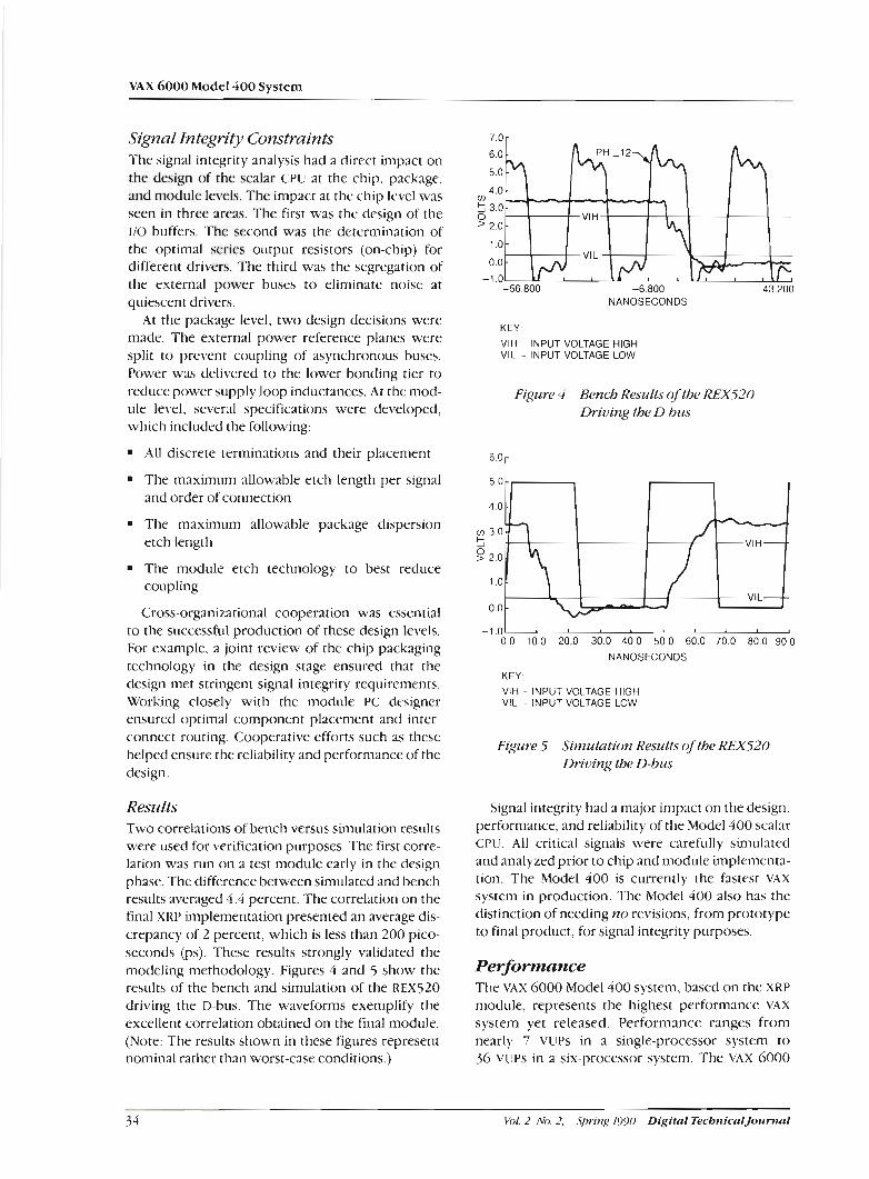
VAX 6000 Model 400 System
Sigtzal Integrity Constraints The signal integrity analysis had a direct impact on the design of the scalar CPU at the chip. package, and module levels. The impact at the chip lcvel was seen in three areas. The first was the design of the 110 buffers. The second was the determination o f the optimal series output resistors (on-chip) for different drivers. The third was the segregation of the external power buses to eliminate noise at quiescent drivers.
At the package level, two design decisions were made. The external power reference planes were split to prevent coupling of asynchronous buses. Power was dclivcred to the lower bonding tier to reduce power supply loop inductances. At the mod- ule level, several specifications were developed, which included the following:
All discrete terminations and their placement
The maximum allowable etch length per signal and order of connection
The maximum allowable package dispersion etch length
The module etch technology to best reduce coupling
Cross-organizational cooperation was essential to the successful production of these design levels. For example, a joint review of the chip packaging technology in the design stage ensured that the design met stringent signal integrity requirements. Working closely with the module PC designer ensured optimal component placement and inter- connect routing. Cooperative efforts such as these helped ensure the reliability and performance of the design.
Results Two correlations of bench versus simulation results were used for verification purposes. The first corre- lation was run on a test module early in the design phase. The difference between simulated and bench results averaged 4.4 percent. The correlation on the final X R P implementation presented an average dis- crepancy of 2 percent, which is less than 200 pico- seconds @s). These results strongly validated the modeling methodology. Figures 4 and 5 show the results of the bench and simulation of the R E X 5 2 0 driving the D-bus. The waveforms exemplify the excellent correlation obtained on the final module. (Note: Thc results shown in thcse figures represent nominal rather than worst-case conditions.)
NANOSECONDS
KEY:
VIH - INPUT VOLTAGE HIGH VIL - INPUT VOLTAGE LOW
Figure 4 Bench Results of the REX520 Driz~ing the D-btls
NANOSECONDS
KEY:
VIH - INPUT VOLTAGE HIGH VIL - INPUT VOLTAGE LOW
Figure 5 Simulation Results of the REX520 Driving the D-bw
Signal integrity had a major impact on the design, performance, and reliability of the Model 400 scalar CPIJ. All critical signals were carefully simulated and analyzed prior to chip and module implementa- tion. The Model 400 is currently the fastest \'AX system in production. The Model 400 also has the distinction of needing no revisions, from prototype to final product, for signal integrity purposes.
Performance The VAX 6000 Model 400 system, based on the X R P module, represents the highest performance VAX system yet released. Performance ranges from nearly 7 VllPs in a single-processor system to 36 VUPs in a six-processor system. The VAX GOO0
34 Vol 2 No. 2, Spring 1990 Digital TecbnicalJottmal
The V U GOO0 Model 400 Scalar Processor Module
Model 410 system provides roughly twice the performance of the previous generation CMOS- based system, the VAX 6000 Model 310. It also represents a 28 percent performance gain over the previous generation ECL system, the VAX 8700 sys- tem. (Note: One VUP is equal to the performance of the VAX-111780 system.)
Table 2 compares the performance of the VAX 6000 Model 410 system to other VAX systems.
Table 2 Single-processor Performance Comparison
System VUPs
VAX 1 11780 VAX 6000 Model 21 0
VAX 6000 Model 31 0
VAX 8700 VAX 6000 Model 41 0
Up to six XRP modules may be configured in a single VAX 6000 Model 400 system. These modules deliver up to 36 VuPs. Ideally, a linear performance increase is expected as more processors are added to a multiprocessor system. However, a number of factors limit the overall system performance, such as contention for bus bandwidth, increased mem- ory latency, and additional software overhead.
A great deal of effort was expended in the Model 400 design to limit the amount of perfor- mance lost in a multiprocessor system.
A number of multistream benchmarks were assembled. 'These benchmarks were run on the VAX 6000 Model 400 system to efficiently measure performance by simulating real work environments across a number of areas. The results for each system are shown in Table 3.
Table 3 Multiprocessor Performance Comparison
WorkArea 1 CPU 2 CPUs 4CPUs 6 CPUs
Engineering 1 .OO 1.92 3.71 5.31 Scientific 1 .OO 1.92 3.74 4.78
Commercial 1 .OO 1.98 3.80 5.25
Acknowledgments The authors would like to acknowledge the follow- ing people for their contributions to the XRP mod-
ule development effort: Dick Bagley, Jean Basmaji, Rick Calcagni, Glenn Gamey, John Guildoo, Andy Ladd, Bill LaPrade, Bob McCarty, Dina McKinney, Curt Miller, Roland Ouellette, Dave RouiUe, John Sweeney, Mike Uhler, mike Warren, and John Wilson.
References
1. H. Durdan et al., "An Overview of the VAX
6000 Model 400 Chip Set," Digital Technical Journal, vol. 2 , no. 2 (Spring 1990, this issue): 36-51.
2. B. Allison, "An Overview of the VAX 6200 Family of Systems," Digital Technical Journal, vol. 1 , no. 7 (August 1988): 10-18.
3. D. Slater et al., "Vector Processing on the VAXvector 6000 Model 400," Digital Technical Journal, vol. 2, no. 2 (Spring 1990, this issue): 11-26.
4 . J. Bartoszek et al., "VAX 6000 Model 400 Physical Technology," Digital Technical Journal, vol. 2, no. 2 (Spring 1990, this issue): 52-63.
5. J. Winston, "The System Support Chip, a Multi- function Chip for CVAX Systems," Digital Technical Journal, vol. 1 , no. 7 (August 1988): 121-128.
6. SPICE is a general purpose circuit simulator program developed by Lawrence Nagel and Ellis Cohen of the Department of Electrical Engi- neering and Computer Sciences, University of California, Berkeley.
Digital TecbnicalJournal Vol. 2 No. 2, Spring 1990 3 5

An Overview of the VAX 6000
W Hugh Durdan William J. Bowhill
John I;. Brown William K Herrick
Richard C. Marcello Sridhar Samudrala
G. Michael Uhler Nicholas Wade
Model 400 Chip Set
The VAx GOO0 Model 400 processor is a CMOS implementation of Digitalk K4X
architecture, offSwing an average of seven times thepe$omnce of the VRY-11/780 processor at a cycle time of 28 ns. The processor c o m p e s five custom chips irnple- rnented in Digital k proprieta y CMOS-1 and CIMOS-2 semiconductor processes. The chg set &st@ incorporates the best features of the previous VRY 8700 and VUf V f l
designs and in addition implements new perfomnce features. Among these are a l a w translation buffer and primary cache, a de-multiplexed 27-bit address and 64-bit data bzls, and a tight& coupled 128KB backup cache. Thefive chips, which are designed for multiprocessing environments, are the REX520 CPU, the floating point accelerator, the VC vector and cache controller chip, the RSSC system support chip, and the CLK clock chip.
Introduction The \)AX 6000 Model 400 chip set consists of five custom VLSI (very large scale integration) chips implemented in Digital's CMOS- 1 and CMOS-2 pro- cesses. The five chips are the CPU chip (REX520), the floating point accelerator chip (F-chip), the vec- tor and cache controller chip (VC chip), the system support chip (RSSC), and the clock chip (CLK chip). These chips are designed to be used in multiple- system environments, of which the vAx 6000 Model 400 series is one such example.'
The REX520 chip is a pipelined VAX CPU that implements the VAX base instruction group and controls the operation of all other chips.* The design for the REX520 is an evolution of both the previous generation CMOS processor chip and the VAX 8800 processor.'." The REX520 is logically divided into four sections: the I-box, E-box, M-box, and bus interface unit (BIU). The I-box fetches and decodes VAX instructions, and provides this infor- mation to the E-box. The microcode-controlled E-box parses instruction specifiers, executes VAX
instructions, and processes interrupts and excep- tions. The M-box contains a 64-entry, fully associa- tive translation buffer, and a 2-kilobyte (KB) on-chip primary cache. The BIU acts as the interface between the REX520 and the interchip environ- ment described below.
The F-chip is a companion chip to the REX520. It accelerates the computation phase of the VAX F-, D-, and G-format floating point instructions, and the longword-length integer multiply instruction. The F-chip receives control information from the REX520, operands from either the REX520, the backup cache, or memory, and returns status and results to the REX520.
The VC chip provides the tag store and necessary control for a 128KB backup cache that is imple- mented in external random access memory (RAJM) on the CPU module. The chip implements a dupli- cate tag store for the REX520 primary cache and an interface through which the system environment can determine if data is cached at a particular address. Through a vector interface bus (V[ B), the VC chip also provides the control and status inter- face between the CPLJ module and an optional vector module.
The Rssc chip incorporates the common core of functions required to support the VAx 6000 Model 400 chip set in a system environment. RSSC supports read-only memory (ROM) and electri- cally erasable programmable read-only memory (EEPROM), and contains 1KB of battery backed-up RAM, the console terminal universal asynchronous receiver/transmitters (UARTs), interval and pro- grammable timers, and a time-of-year clock.
36 Vo1. 2 1Vo. 2, Spring 1930 Digital TecbnicalJournal

An Overview o f the VAX 6000 Model 400 Chip Set
The CLK chip receives a 143-megahertz (MHz) oscillator input. The chip provides four low-skew clock phases to the chip set and the module environment.
Interchip and Module Environment The chips in the Model 400 chip set are connected together and to the rest of the module environment as shown in Figure 1.
Unlike the previous generation CMOS processor design" the Model 400 chip set implements sepa- rate 27-bit address and 64-bit data buses. Backup cache reads, writes, and fills are done with the address on the A-bus. The data is driven to or received from the parity protected D-bus. Control for the backup cache RAMS is provided by the VC chip on dedicated control lines.
Memory, 110 space, and external processor regis- ters are accessed by driving the address to the A-bus and the data to the D-bus. ROM and EEPROM control is provided by the RSSC on dedicated control .lines.
F-chip operands are driven to the D-bus from the REX520, backup cache, or memory to the F-chip. Results are driven back to the REX520 on the D-bus. Control and status information for these transfers is performed on a private bus between the REX520 and F-chip.
Vector instructions are decoded by the REX520. The opcode and instruction operand information is transferred from the REX520 to the VC chip. From there, the information is transferred to the VlB cable and then to the optional vector unit. Note that only status and scalar operands (contained within the instruction stream) are transferred on the VIB. Data
transfers into and out of the vector register f ie are performed by the vector processor through a direct port to the memory subsystem.
Interrupt requests are received by the REX520 from the module environment on nine dedicated interrupt request lines. Five of these lines are for requests for special purpose interrupts, such as interval timer requests.
Per$omzance Goals and Design Considerations The goal of the design was to meet or exceed the performance of the VAx 8700 processor. To meet this goal, a 40-nanosecond (ns) cycle time was required under worst-case conditions. As the design progressed, it became clear that the CMOS-2 pro- cess, in which most of the chip set is implemented, offered enough performance to allow the target cycle time to be decreased.
As a result, the cycle time was reduced from 40 ns to 28 ns. At this cycle time, the VAX 6000 Model 4 10 system runs at nearly 7 vUPs in most applica- tions, or roughly 1.3 times the performance of the VAX 8700 processor. (The acronym VUPs stands for VAX units of performance; 1 V U P equals the perfor- mance of a VAX-111780 system.) The performance of the system may be further expanded by adding processors to the system, to a maximum of 35 VUPs in the VAX 6000 Model 460.
To achieve the performance goals, a number of microarchitectural trade-offs were made relative to the \,AX 8700 and previous VLSI VAX designs. In essence, the best features of each were incorporated into the design of the \'AX 6000 Model 400 chip set.
A-BUS
VIB CABLE
4 A D-BUS
INTERRUPT 1 CONTROL. 1 1 1 CONTROL, 1
Figure I VAX 6000 Model 400 Interchip Environment
Digital TechnicalJoumal VoL 2 No. 2, Spring 1990 37
RSSC ROM. EEPROM
REQUESTS
CLOCKS ! t t " t t
REX520 STATUS - F-CHIP
CONTROL VC CHIP w R A M S

VAX 6000 Model 400 System
For example, the REX 520 chip and the F-chip are fully pipelined designs that make shorter cycle times possible and improve performance. The RI:XjZO design also includes read-and-run and write-and-run features. These features decouple subsequent execution in the CPU pipeline from the completion of references to cache and memory. As opposed to previous VLSI designs, a larger transla- tion buffer and primary cache and a de-multiplexed 27-bit address and 64-bit data bus in the REX520 also improve performance. The tightly coupled 128KR backup cache significantly reduces the read latency sccn by the CPU when a read misses in the primary cache. I t also reduces the read traffic seen by the memory subsystem.
The chip set was designed from the beginning with multiprocessing in mind. Becausc caches must remain coherent across all CPUs in a system, a method must be provided to invalidate cached loca- tions in all other caches when one cPr: writes to that location. One option would have been to mir- ror all writes done by any CPU in the system onto the A-bus of all C131's. However, mirroring is a rela- tively expensive operation, especially when most of these addresses are not cached in any other CPU.
Instead of the mirroring method, we chose to implement a duplicate copy of the primary cache tag store in the VC chip and to implement a low- overhead port, the I-bus. The module environment uses the I-bus to determine if the address is actually cached by either the primary or the backup cache. With this method, only those invalid addresses that correspond to cached locations must be mirrored onto the A-bus.
CMOS and Packaging Technologies The chip set was implemented in Digital's proprie- tary second-generation complementary metal oxide semiconductor technology, CMOS-2. We selected CMOS as the chip processing technology because it offers high density, high reliability, low power, and low-cost performance.
Table 1 Summaw of Chip Statistics
By developing the technology in-house, Digital has gained competitive performance and tirne-to- market advantages for its low-end and midrange products. A summary of the transistor and pin- count statistics for the chip set is shown in Table I .
CMOS-2 is an N-well, P-epitaxial, double-metal, 5-volt process with 1.5 micron minimum feature sizes. With respect to CMOS-1, the first generation process, CMOS-2 offers a 25 percent reduction in lateral and key vertical dimensions, a 78 percent improvement in circuit density, and nominally a 33 percent improvement in chip performance. The VAX 6000 Model 400 chip set cycle time and cir- cuit density requirements helped drive the develop- ment of the process that has been optimized for microprocessor chip performance. Details of the process features and capabilities are shown in Table 2.
Metal oxide semiconductor field effect tran- sistors (MOSFETs) are built in a P-epitaxial layer (30 ohm-cm) grown on a low-resistance P+ silicon substrate (0.02 ohm-cm). The high resistance of the epitaxial layer keeps parasitic junction capacitance low and allows better transistors to be fabricated. The low-impedance substrate dramatically reduces latchup, a phenomenon in which parasitic bipolar transistors are triggered into a sustained high cur- rent mode. Latchup disrupts normal circuit opera- tion and often destroys the chip.
The P-channel MOSFETs are made in the N-doped well regions of the epitaxial layer. The N-channel MOSFETs are made in the as-grown P-regions of the epitaxial layer. This process optimizes the mobility of the N-channel MOSFETs and overall circuit speed.
An N+ polysilicon (polycrystalline silicon) and tungsten-disilicide sandwich material, polycide, forms the MOSFET gates. Polycide resistance is in order of magnitude lower than that of the poly- silicon used in CMOS-1. The resulting smaller para- sitic delays across the MOSFET gates and local interconnections help improve circuit speeds.
Transistor Count
Chip Signal Power Control 81 Pins Die Size Dissipation Memory Data Path
-
REX520 CPU 157 12mm x 12mm 6W 180K 140K VC cache controller 178 10.7mm x 10.8mm 2.5W 184K 34 K F-chip floating point 103 12.7mm x 11 mm 4W - 134K
CLK clock 2W Total:
38 Vol 2 No. 2, Spring 1330 Digital TecbnicalJo~~rnul

An Overview of the VAX 6000 Model 400 Chip Set
Table 2 CMOS-2 Process Features and Capabilities
Effective channel length Metal 1
Metal 1 contact
Metal 2 Metal 2 contact
Gate oxide thickness Metal 1 field oxide Metal 2 field oxide Polycide resistance
Typical gate delay Polycide equivalent gate delay length
Metal 1 equivalent gate delay length
0.9 microns 3.0 micron width, 1.5 micron space
1.5 micron x 1.5 micron
3.75 micron width, 1.5 micron space 1.5 microns x 1.5 microns 225 angstroms 1.1 microns
1.9 microns 2-4 ohmslsquare
300-500 picoseconds 400 microns 5000 microns
Metal 2 equivalent gate delay length 8000 microns
Other interconnections are accomplished through two layers of aluminum. The f i s t layer, metal 1, can connect to either polycide or the N+/P+ sourcetdrain regions via metal 1 contacts. The upper layer, metal 2, can connect to metal 1 through metal 2 contacts. No other connections are allowed. Based upon its parasitic delay charac- teristics, polycide is used only for local interconnec- tions. Metal 1 is used for signals communicating across distances less than half of the chip dimen- sions. Metal 2 is used for global signals, clock dis- tribution, and power and ground distribution.
Because of the speeds and complexities of the VAX 6000 Model 400 chips, noise is a particularly difficult problem for the chip designer. CMOS-2 contains a deep P+ implant that can be used to provide a very low resistance connection between the top surface of the chip and the P+ substrate. The chip designer uses this deep P+ implant to reduce substrate noise that can upset the operation of dynamic circuits.
The VAX 6000 Model 400 chips were packaged in custom-designed, rigid perimeter-leaded, single- chip ceramic packages. The packages included four power and ground planes to help maintain inter- chip signal integrity and allow full-speed operation of the chip set.5
The REX520 CPU Chip The REX520 CPU chip is a third-generation, single- chip vAX microprocessor. The REX520 provides the hardware and microcode sufficient to parse operand specifiers, execute instructions, and han- dle interrupts and exceptions. It cooperates with the F-chip to implement the base instruction group of the Vtuc architecture.
Although the REX520 hardware organization and placement resemble that of the previous gener- ation microprocessor, the REX520 performance goals were met by tailoring the microarchitecture more closely to the VAX 8700 processor."hny deviations from the microarchitecture of the ECL- based VA?i 8700 system were made in the CMOS- based REX520 to compensate for technology differences and to exploit the beneficial aspects of VLSI design. A photomicrograph of the REX520 is shown in Figure 2.
The chip employs a six-level pipelined engine built around three autonomous pipes. These pipes provide simultaneous instruction prefetch and decode, instruction formatting, operand reference, execution, address translation and result store, and 110 access.
As shown in Figure 3, the major hardware functions of the REX520 are partitioned into the following:
An instruction box (I-box) that contains the instruction decoder and a 16-byte prefetch queue (PFQ)
A microcode-controlled execution box (E-box) that provides the capability for data manipu- lation in a 32-bit data path
A memory box (M-box) that implements VAx
memory management by utilizing a 64-entry, fully associative translation buffer
A 2KB write-through, direct-mapped primary cache (P-cache) with a quadword (8 byte) fi size
A bus interface unit (BIU) that controls a fully handshaked, synchronous chip bus
Digital TecbnicalJournal Vol. 2 .No. 2, Spring 1990
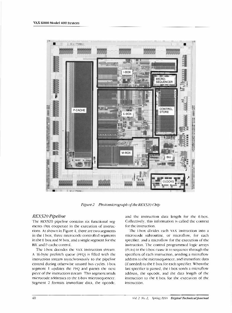
VAX 6000 Model 400 System
Figure 2 Photomicrograph of the REX520 Chip
REX520 Pipeline The REX520 pipeline contains six functional seg- ments that cooperate in the execution of instruc- tions. As shown in Figure 4 , there are two segments in the I-box, three microcode-controlled segments in the E-box and M-box, and a single segment for the BIU and P-cache control.
The I-box decodes the vAX instruction stream. A 16-byte prefetch queue (PFQ) is filled with the instruction stream asynchronously to the pipeline control during otherwise unused bus cycles. I-box segment 1 updates the PFQ and parses the next piece of the instruction stream. This segment sends microcode addresses to the E-box microsequencer. Segment 2 formats immediate data, the opcode,
and the instruction data length for the E-box. Collectively, this information is called the context for the instruction.
The I-box divides each vAX instruction into a microcode subroutine, or microflow, for each specifier, and a microflow for the execution of the instruction. The control programmed logic arrays (I'LAs) in the [-box cause it to sequence through the specifiers of each instruction, sending a microflow address to the microsequencer, and immediate data (if needed) to the E-box for each specifier. When the last specifier is parsed, the I-box sends a microflow address, the opcode, and the data length of the instruction to the E-box for the execution of the instruction.
40 R)I. 2 No. 2, Spring 1990 Digftal TecbnicalJournal

An Overview of the VAX 6000 Model 400 Chip Set
MICROFLOW ADDRESS
MICROSEQUENCER
MICROINSTRUCTION 4.1- ADDRESS-'
MICROINSTRUCTION
DATA BUS
Figure 3 REX520 Block Diagram
The I-box pipeline runs autonomously to the E-box pipeline. That is, the I-box segments con- tinuously parse instruction stream data, making microflow addresses available. The 1-box pipeline advances whenever the microsequencer accepts a microflow address.
The microsequencer in the E-box performs a read of the 1696 word control store each cycle, overlap- ping in time with I-box segment 2. It presents the
fetched microinstruction to E-box segment 1. The microinstruction is pipelined forward to E-box seg- ments 2 and 3 in consecutive cycles.
The microsequencer fetches one or more microinstructions of a microflow starting at the initial microflow address supplied by the I-box. If a microflow contains more than one micro- instruction, the microsequencer computes subse- quent intraflow microaddresses and fetches the corresponding microinstructions. A field within the microinstruction indicates the end of each microflow.
The E-box performs all the address and data manipulation required for the REX520 to adhere to the VAX architecture. The three E-box segments operate under microinstruction control; the operand fetch segment reads operands from gen- eral-purpose registers (GPRs) or from the memory data (MD) file and presents them to the functional units; the execution segment performs data manip- ulation on the operands; and the result store seg- ment writes results to registers or memory. The E-box pipeline segments are fully folded, i.e., each segment simultaneously operates on a different microinstruction.
The performance of memory read accesses is improved using a read-and-run technique in the E-box. The destination for data stream memory reads is the E-box MD file. Microinstructions that initiate a memory read simply queue the request to the BlU. The microflow may then continue, without waiting for the request to complete. In this manner,
CACHEACCESS
I-BOX SEGMENT 1
INSTRUCTION PARSE AND DECODE
MICROFLOW ADDRESS GENERATION
Figure 4 REX520 Pipeline Segments
Digital TecbnicalJournaL Vol. 2 No. 2, Spring 1990 4 1
1 BIU/P-CACHE SEGMENT 1
E-BOX/M-BOX SEGMENT 3
RESULT STORE
ACCESS CHECKING
I-BOX SEGMENT 2
INSTRUCTION DATA AND CONTEXT FORMATTING
CONTROL STORE ACCESS
E-BOX/M-BOX SEGMENT 1
OPERAND FETCH
4 +
E-BOX/M-BOX SEGMENT 2
EXECUTION
VIRTUAL ADDRESS SELECTION A N D TRANSLATION

VAX 6000 Model 400 System
some or all of the time required for memory accesses is hidden during productive microflows. The request completes when the B ~ u and memory subsystem return data to the MD file.
Because subsequent microinstructions may refer- ence an MD file location for which a memory read has not yet completed, M D file accesses are syn- chronized through a valid bit mechanism. Each MD
file location has a valid bit that is reset when a mem- ory read is started. The bit is then set when data is written to the file. If a microinstruction attempts to reference an MD file location whose valid bit is not set, the pipeline stops advancing (stalls) and waits for the data to be returned.
The three M-box segments are microcode- controlled and typically run synchronously with the E-box segments. M-box segment 1 decodes the current microinstn~ction. Segment 2 then selects an appropriate address source and performs a vir- tual to physical address translation if required. The final segment issues the physical memory request to the BIU.
During normal pipeline flow, the BIU and P-cache operate in a single pipeline segment which is over- lapped with segment 3 of the E-box/M-box pipeline. The BIU acts as an arbiter for the external and some internal buses, and supplies control to the P-cache. The BIU receives address and memory request information from the M-box. The BIU then decides whether the M-box or an external reference should receive service from the P-cache and sends the appropriate information to the p-cache to process the request. The BIU sends read and write requests that cannot be serviced by the P-cache to the off- chip memory subsystem.
Write buffers in the BIu improve the perfor- mance of memory write operations. Microinstruc- tions that initiate memory writes queue the request to the BIU, and the microflow continues without waiting for the request to complete. In this manner, the time required for memory writes can be hidden under productive microflows. The BIU can store up to two quadword writes (32 bytes) in its buffers while waiting for the memory subsystem to become available.
Adaptations for VLSI VLsI designs have relatively good signal integrity on the major bus structures within a chip. However, signal integrity diminishes when crossing a chip boundary because off-chip bandwidth is incapable of sustaining the internal data rates. This character- istic of VLSl design influences microarchitecture
greatly, as demonstrated by the P-cache and control store designs.
The \'AX 8700 system uses cache memory to decrease the effective memory access time by employing a 6 4 ~ ~ cache in ECL RAM with a single- cycle access. I t was not possible to implement a RAM of this size on the REX520, and signal integrity constraints dictated a minimum of three cycles to access off-chip RAM. The REX520 compensates by using a two-level cache. The REX520 has a 2KB pri- mary cache on the chip with a single-cycle access, and there is a 128KB off-chip secondary cache. The cache hierarchy reduces the effective memory access time sufficiently to meet the performance goals, and it keeps the off-chip bandwidth within reasonable rates.
Similar signal integrity constraints are imposed on the REX520 control store design. The V k Y 8700 system uses a 16K entry control store implemented in ECL RAM. The VAX 8700 system designers use the large control store address space to improve per- formance and simplify hardware. The control store access of the VLSI REX520 cannot cross a chip boundary and keep pace with the fast internal cycle time. Because of these limitations, an on-chip con- trol store ROM was used. Chip area limitations con- strained the size to 1696 entries. The designers of the REX520 compensated for the lack of control store address space by altering the coding style to make microflows more serial than the VAX 8700 system microflows. Additional hardware features also helped to absorb some of the work previously done in microcode.
The operand specifier microflows offer an exam- ple of microcode space compression facilitated through hardware enhancements. The REX520 microflows group similar specifier types together and provide a general routine for each. The general routines are parameterized in hardware to resolve the differences in specifier types within each group. In this way, the size of the microflow is minimized, and the performance characteristics of a dedicated microflow are preserved.
Each general specifier microflow performs the function appropriate to the specifier mode by using a parameterized access type and data length. For example, a microinstruction in the specifier flows may make an access-type dependent memory request. I f the I-box supplied a read access type, the memory request hardware initiates a read. If the I-box parsed a result store specifier, the write access type parameter causes hardware to initiate a write. Operand data length is supplied in a similar fashion.
kt)/, 2 No 2, Sp17ng I990 Digital TechnicalJoumnl

The general microflows leave operands in futed locations in the E-box MD file. The exact location in the MD file is also supplied by the I-box.
Parameterizing the microflows with the access type, data length, and MD file location allows the generalized specifier rnicroflows to be shared. The MD file parameter creates an independence between the specifier and execution microflows. The same specifier microflow can then be used for each specifier mode, independent of where it actually appears in the instruction. The execution
y STAGE 4
An Ovm~iew of the V M 6000 rModel400 Chip Set
microflow also needs to know nothing about the kind of specifier that supplied the operand.
me F-chip The floating point accelerator chip, F-chip, is the companion processor chip to the REX520 for floating point operations in VAX 6000 Model 400 systems. A photomicrograph of the chip is shown in Figure 5.
The F-chip implements all \rAX base instruction group floating point instructions and the longword
ADMR [
'ERFACE = - - .
Figzire 5 F-chip Photomicrograph
Digital TechnicalJournaI Vol. 2 No. 2, Spring 1970 4 3

VAX 6000 Model 400 System
integer multiply instruction. The data types irnple- mented by the F-chip are F-floating (1-bit sign, 8-bit exponent, 24-bit fraction), D-floating (I-bit sign, 8-bit exponent, 56-bit fraction), G-floating (1-bit sign, 11-bit exponent, 53-bit fraction), and integers (8-bits, 16-bits, and 32-bits).
Unlike the VAX 6000 Model 200 floating point chip, the F-chip employs a uniformly pipelined architecture that has performance which is inde- pendent of the operand values. Early in the design it was decided to use a pipelined microarchitecture in order to use the same execution core in future designs, such as the VAX 6000 Model 400 vector processor floating point unit. Consequently, the execution core of the F-chip was designed to include low latency for scalar applications and high throughput for vector processing.6 The core exe- cutes most instructions in four cycles. Double- precision and integer multiply instructions take five cycles, and divide operations take 13 to 24 cycles, depending upon the data type.
Microarchitecture and Imphentation The F-chip is composed of an interface section and a five-stage execution core. A block diagram of the F-chip is shown in Figure 6. The F-chip interfaces to the rest of the VAX 6000 Model 400 system through the D-bus, eight status and control lines, and four bus control signals. The interface section receives the opcode from the REX520, the operands from the CPU chip, and cache and memory data on the D-bus. The interface section decodes the opcode and receives the required number of operands. It assembles the different pieces of the operands and supplies formatted operands to the execution core. After the execution of the floating point operation, the output interface transfers the formatted result back to the CPU chip.
The execution core consists of a divider, which is bypassed in all operations except division, and four pipelincd stages that are uniformly utilized in the execution of all instructions. Each stage has a frac- tion data path, control, and sign and exponent data
INPUT IMTERFACE
t t t t I 1
DNIDER n CONTROL
I I I I I I
4 t + 4
PI I
t t t t
Figure 6 F-chip Execution Core
t * t *
Vol. 2 No. 2, Spritig 1990 Digital TechnicalJournal
I I I I
STAGE 2
CONTROL
[a -1 NORMALIZER cc
ExpONENT PROCESSOR
- CONTROL -
+ - ADDER - CONTROL o PROCESSOR
STAGE
OUTPUT INTERFACE
PROCESSOR
STAGE 1
CONTROL STAGE 3
- -
PROCESSOR

An Overview of the VXX 6000 Model 400 Chip Set
paths. The fraction data path, the most complex portion of the chip, is 60 bits wide.
The divider fraction data path consists of the hardware divider array and quotient logic. The divider array implements an iterative radix-2 SRT nonrestoring division scheme, and generates three signed quotient bits per cycle.' The quotient and remainder are driven on consecutive cycles to stage 1 of the pipeline.
The stage 1 fraction data path consists of a 60-bit adder, the multiplier recode logic, and the fraction detection logic. Stage 1 receives its inputs from the interface section, or from the divider for divide operations. In add and subtract operations, stage 1 is used primarily to compute the difference between the exponents of the two operands. In parallel, stage 1 is also used to determine the frac- tion difference for exponent differences of 0 and 1.
FRACTION 1 FRACTION 2
CONTROL R SlGN 1
EXPONENT 2
CONTROL 0 SHIFT A M O U N T
CONTROL n SlGN A N D EXPONENT C
FRACTION R E S U L T SIGN EXPONENT RESULT RESULT
Figure 7 F-chip Hardware for Addition and Subtraction
(See Figure 7.) For the effective subtract operation, stage 1 uses an exponent difference prediction scheme in which the least significant two bits of the two exponents are examined to determine whether 0 or 1 bits of alignment are required.
If the actual exponent difference is 0 or 1, stage 1 selects the adder result. Otherwise, stage 1 passes the original operands to the next stage for align- ment. In multiplication flows, the: stage 1 adder is used to compute three-times the multiplicand, and the recode logic generates the recoded multiplier bits for stage 2. In divide operations, stage 1 is used to assimilate the redundant quotient and remainder vectors into a two's complement form.
The stage 2 fraction data path consists of a dynamic 57-bit right shifter, unified leading one or sticky-bit detection logic, and a multiplier array. (The sticky-bit indicates whether a "1" was shifted out of the data path during alignment operations.) The shifter is used in add-like operations for align- ing the fractions. The leading one or sticky-bit logic determines the normalization amount during sub- tract operations and integer-to-floating-point con- versions. This logic also determines the sticky-bit during alignment in effective subtract flows. The multiplier array implements a radix-8 modified Booth algorithm and consists of nine carry save adder (CSA) rows. It is traversed once for single- precision formats and twice for integer and double- precision formats. The hardware organization for the multiply operation is shown in Figure 8.
Stage 3 of the pipeline consists of a 60-bit adder and a 57-bit dynamic left shifter for normalizing the intermediate results. The fraction adder is used in multiply operations to assimilate the product sum and carry vectors, and in add-like flows to add or subtract the aligned operands.
Stage 4 of the pipeline consists of a 60-bit adder used for rounding and negation of the final result, and the exception detection logic. The exception handling is done with a PLA which detects and sig- nals overflow, underflow, zero results, and invalid operands.
The control is hardwired (no microcode is used) and distributed among the pipeline stages. Each stage has autonomous control implemented with control decoder PLAs. Each stage supplies control information to the next stage one cycle ahead of the data. This enables the data path control signals to set up before the data is propagated to the input of the stage. The distributed control scheme permits simultaneous execution of a divide and four other instructions in the pipeline.
Digital TecbnicalJournnl Vo1. 2 No. 2, Spring I990 4 5

VAX 6000 Model 400 System
FRACTION DATA PATH
MULTIPLICAND
ADDER
3X MULTIPLICAND
RECODER/IPPR
N SELECT W a 2 0
KEY:
SF. CF S U M AND CARRY OUTPUTS TC TWO'S COMPLEMENT VECTOR IPP INITIAL PARTIAL PRODUCT S, C SUM A N D CARRY INPUTS PR PRODUCT FP FRACTION PRODUCT
Figure 8 F-chip Multiplication Fraction Data Path
The exponent data path in each stage is 13 bits wide. Each stage has a 13-bit adder and detection logic for detecting zero operands, exponent differ- ences, and exception conditions. To compute the absolute value of the exponent difference in add, subtract, and convert operations, the stage 1 expo- nent data path has an additional 13-bit adder and selection logic.
The microarchitecture and the hardware orga- nization of the F-chip were chosen to efficiently implement the three basic operations addtsubtract, multiply, and divide. As an example of this effi- ciency, the adder in stage 1 is used in both the effective subtract flow and the multiplication and division flows. This flow overlap permits the execu- tion of effective subtraction in only four steps, inde-
pendent of the data, as opposed to five steps without the overlap.
For multiplication, this organization enabled the use of a radix-8 algorithm, which requires the computation of three-times the multiplicand. The implementation of all other operations was realized with the addition of minimal logic.
The VC Chip The VC chip, or the backup cache controller and vector interface chip, implements the second level of a two-level cache structure and the interface to an optional vector processor. A photomicrograph of the vC chip is shown in Figure 9.
Cache Control Functions The R E X 5 2 0 contains a 2KB primary cache data and tag store. The VC chip contains the tag store and control logic to perform reads, writes, and invali- dates to a 1 2 8 K B secondary, or backup, cache. The backup cache is direct-mapped and write-through.
The VC chip backup cache tag store is organized such that one tag and four valid bits correspond to every four-octaword (64-byte) block of the cache. Each valid bit corresponds to a one-octaword sub- block, as illustrated in Figure 10. When a cache tag miss occurs on a read, a block is allocated, a sub- block is filled, and the corresponding valid bit is set. When a cache tag compare is successful but the valid bit is not set, a sub-block is filled from memory and the corresponding valid bit is set.
The Backup Cache Data Store The backup cache data store is built with off-the- shelf CMOS static RAMS, which are located on the module. The discrete cache data RAMS are orga- nized as 8 bytes wide (the width of the D-bus) by 16,384 locations deep. In addition, there are eight bits of parity, with one bit corresponding to each data byte. Fourteen bits of the VAX physical address are needed to access the cache, as shown in Fig- ure 1 1 . When the backup cache returns data to the R E X 5 2 0 primary cache, it returns one quadword, the fill size of the primary cache.
The Invalidate Filter Bus, I-bus As mentioned, the chip set implements a special- purpose bus, the I-bus, that allows the memory subsystem filter invalidates. In addition to this bus, the VC chip also implements a copy of the R E X 5 2 0 primary cache tag store for invalidate filtering.
1/01. 2 No. 2 5pring 1990 Digital TecbnicalJournal

An Overview of the VHX GOO0 Model 400 Chip Set
. ' V ' '
BYTE MASK AND , . CHlP SELECTS
CACHE CONTROL 1 LOGIC
Figure 9 VC Chip Pbotomicrograpb
VALID BITS BACKUPCACHE
ONE SUBBLOCK (FILL SIZE)
FOURTH VALID BIT
OCTAWORD 3 I
SECOND VALID BIT OCTAWORD 1
Figure 10 Tag, Valid Bits, and Backup Cache Store
VC CHlP TAG STORE
Digital TechnicalJournal Vol 2 No. 2, S/~rr?rg I990
THIRD VALID BIT OCTAWORD 2
ONE BLOCK - (ALLOCATION SIZE)

VAX 6000 Model 400 System
ADDRESS BIT
I I CACHE ENTRY TAG I I1 1/0 SPACE. NOT CACHED 1 I
BACKUP CACHE INDEX
UNUSED !-I Figure 11 VAX Pbydxzl Aliciress and Backup
Cache RAMS
When an address is sent to the VC chip on the I-bus, the VC chip notifies the memory interface as to whether or not the address produced a hit in either cache. The memory subsystem broadcasts the invalidate onto the A-bus only if a match was detected. This mechanism significantly improves performance in multiprocessor systems by reduc- ing the overall traffic on the processor buses.
The Vector Interface The VC chip implements the interface logic that allows an optional vector unit to bc connected to the scalar processor module. The vector unit has the potential to significantly increase the perfor- mance of many analytical applications.
If the vector unit is present in the system, the R E X 5 2 0 scalar CPU chip decodes vector insuuc- tions and passes operand and control information to the vector module through the VC chip vector interface. The vector unit, using its own memory interface, accesses vector data from memory.
The vector and scalar n~odules are connected through the vector interface bus (VIB). The VC chip is the sole master of the VlB. The VlB is asyn- chronous to the VC chip and synchronous to the vector module The VC chip implenicnts the asyn- chronous control logic required for transferring data between the two modules. The clecision to operate the VIB asynchronously with respect to the VAX 6000 Model 400 mcxlule was made in order to simplify the &sign of the vector modulc.
Xbe RSSC Chip A variety of support logic is required to com- plete the functionality of a VAX CPr: module. The VAx 6000 Modcl 400 systcm support chip (RSSC) integrates on a single chip the common core of functions necessary to support the VAX system environment. A photomicrograph of the RSSC is shown in Figure 12.
The RSSC provides the operating system with the hardware primitives needed to implement the boot and console routines, and with several mcssary timing mechanisms. The RSSC is designed to inter- face directly with the VAX GOO0 Model 400 chips, and is based on the system support chip, or ssc.'
The decision to base the RSSC chip on the previ- ous SSC design was made because we could take advantage of an existing core of logic which already implemented the required functions. The SSC was fabricated in the CMOS-1 process and had been thor- oughly debugged and qualif~ed for the MicroVAX 3500/3600 system.' The challenge faced by the RSSC team was to design a new pad ring and bus interface unit (BIU) that would interface the existing SSC core to a much different and faster interchip environment.
RSSC Functions The functions that the RSSC provides for the VAX 6000 Model 400 module can be grouped into two categories: boot and console code support, and timer functions to support the operating system.
Some of the important console and boot code support functions contained in the RSSC are the ROMIEEPROM interface, CPU halt-request protec- tion, UARTs with programmable baud rates, 1 KB of standby RAM, am! input and output ports which interface to several console and module-level switches and LEDs. The RSSC also implements three timer functions: the bus timeout counter, a 10-milli- second interval timer, and a time-of-year clock.
The CLK Chip Clock generation for the VAX 6000 Model 400 chip set was placed in a separate chip, the CLK chip, to better control interchip skew. By separating the clock, we eliminated power, pin count, area, and noise problems from the other possible home of the clocks, the REX520. Three main factors were taken into account in designing the CLK chip. These fac- tors were the number of clock edges, clock skew, and signal integrity. A photomicrograph of the CLK chip is shown in Figurc 13.
In determining the optimal configuration for the number of clock edges, the CMOS micro- architecture was examined closely. The number of clock cdges per microcycle determines the granu- larity available to the designer. Increased granular- ity can simplify the design process by reducing the need for self-timed design techniques. However, the usefulness of partitioning the design cycle is limited. Granularity on the order of a gate delay is of
Vol. 2 No. 2, Spring 1990 Digital Technical Journal

An Ovmieu , of the I/AX 6000 Model 400 Chip Set
Fzgz~re 12 RSSC Photomicrogruph
little use, whereas granularity on the order of a microcycle imposes the use of self-timed circuits. A decision was made to distribute four 14-ns pulses phased in timc by 7 ns to facilitate the design of regular arrays, data path structures, and 110 func- tions. This distribution made master-slave clock generation and single-phase generation easy, and complementary clocks for latches more available.
Clock skcw was minimized through logic and circuit techniques. The clocks are generated from a 1 4 3 - ~ ~ z crystal oscillator. The frequency is imme- diately divided by two to generate an even duty cycle 71.5-MHz signal and its complement (PHI and PHI-BAR). The divide circuitry, which comprises
four D-type flip-flops, is shown in Figure 14. CLK is the clock input, D is the data input, Q is the latched true data output, and QB is the latched complement data output.
CLK is the 143-MHZ crystal oscillator clock. The circuit consists of a D-typc flip-flop with one mas- ter, Dl, and three slaves D2, D3 , and ~ 4 . D2 pro- vides local feedback for the divide-by-two function in order for D3 and D4 to match identically. D 3 is the Q slave and D4 is the Q B slave.
D3 allows the inversion in the feedback path to be absorbed and the Q and QB to see the same num- ber of gate delays. This logic technique works for all dividers used in the design. However, the
Digital TecbnfcalJournal Vol. 2 No. 2, Swing 1990 4 c)

Fzgure I3 CLK Chip Photomicrograph
dividers feed a series of large output drivers in package, three power pins, three ground pins, and which skew could not be controlled through logic two signal pins were used for each driver. techniques. In these cases, skew was minimized This pin design reduced the inductance seen by by matching the capacitance on each node. The end each driver by approximately a factor of two. In result was a design in which the skew between any two edges genirated by the CLK chip was ndt greater than 0.3 ns.
Signal integrity was carefully considered in the design. The clocks had to be distributed to eight different loads, and the total skew between any two edges could not exceed 0.5 ns. This design implied that the Cl,K chip package and the clock module interconnect could not contribute more than 0.2 ns of skew. To mininuze the electrical impact of the F i ~ u r e 14 CLK Chip Divide Circuitry
50 I/,)/. 2 No. 2, Sl~ring l00O Digital TechnicalJournal
D
- C
--
CLK
- Q D Q
D l D3 QB 4 c QB
- Q D D
D2 D4 08 C 3 O C QB
rnl
PHI-BAR

An Overview of the VAX GOO0 Model 400 Chip Set
addition, the clocks were radially distributed, and diode termination was used on each clock leg. The length of each leg was identical.
Conclusions The VAX 6000 Model 400 chip set represents a suc- cessful mapping of the ECL-based VAX 8700 system microarchitecture into a CMOS-based VLSI chip set. The fully folded pipeline, on-chip cache and control store, and read and runtwrite and run strategies of the processor chip, combined with a high perfor- mance floating point processor and a second-level cache, enabled the VAX 6000 Model 400 to exceed the original performance goals for the system.
Achowkdgments The authors would like to acknowledge the follow- ing people for their contributions to the VAx 6000 Model 400 chip set development effort: Randy Allmon, Brad Benschneider, Mary Jo Butler, Sandy Carroll, Gerry Cheney, Larry Commodore, Beth Cooper, Amnon Fisher, Nannette Fitzgerald, Annette Flohr, Moshe Gavrielov, Ed Gomes, Paul Gronowski, Bill Grundmann, Ellen Kagan, David Kravitz, Liam Madden, Vijay Maheshwari, Steve Martin, Karen McFadden, Roger Meeks, George Mills, Mike Minardi, Millind Mittal, Dave Morgan, Victor Peng, Jeff Pickholtz, Jim Reinschmidt, Doug Sanders, Katie Siegel, Rebecca Stamm, Pete Starvaski, Bob Supnik, Bill Wheeler, Jeff Winston, and Bill Upham.
References
1. P. Sullivan et al., "The VAX 6000 Model 400 Scalar Processor Module," Digital Technical Journal, vol. 2, no. 2 (Spring 1990, this issue): 27-35.
2. T. Leonard, ed., VMX Architecture Reference Manual (Bedford: Digital Press, Order No. E Y - 3 4 5 9 ~ - ~ ~ , 1987).
3. T. Fox et al., "The CVAX 78034 Chip, a 32- bit Second-generation VAX Microprocessor," Digital Technical Journal, vol. 1, no. 7 (August 1988): 95-108.
4. S. Mishra, "The VrU< 8800 Microarchitecture," Digital TechnicalJournal, vol. 1, no. 4 (February 1987): 20-33.
5. J . Bartoszek et al., "VAX 6000 Model 400 Physical Technology," Digital Technical Journal, vol. 2 , no. 2 (Spring 1990, this issue): 52-63.
6. B. Benschneider et al., "A Pipelined 50-MHz CMOS 64b Floating Point Arithmetic Processor," IEEE Journal of Solid State Circuits, vol. 24, no. 5 (October 1989): 1317- 1323.
7. D. Atkins, "Higher Radix Division Using Esti- mates of the Divisor and Partial Remainders," lEEE Transactions on Computers, vol. C-17 (October 1968): 925-734.
8. J. Winston, "The System Support Chip, a Multi- function Chip for CVAX Systems," Digital Technical Journal, vol. 1 , no. 7 (August 1988): 121-128.
9. G. Lidington, "Overview of the MicroVAX 35001 3600 Processor Module," Digital Technical Journal, vol. 1, no. 7 (August 1988): 79-86.
Digitul TecbnicnCJoumal Vo1.2 No. 2, Sp'ng 1990 5 1

John T. Bartoszek Robert J. Hannemann
Stephen P. H a m e n RobertJ. McCarty John C. Sweeney
VAX 6000 Model 400 Physical Technology
The physical realization of the VRY GOO0 Model 400 microprocessor design offered a number of significant challenges at both the chip package and the module levels. In meeting the req~rirements for a robust and man~lfncturable midrange imple- mentation, the K-tY 6000 Model 400physical technology approach broke new ground for Digital, and, in some cases, for the indmtry. New developments included the first tape-automated bonding (W) interconnected senziconducton, extensive board-level physical sirnz~lation, and the use of advanced testability features on a microprocessor-based midrange product. i%ispaperprovhies details of thephysi- cal tech?zology used in the 1IM GOO0 Model 400 project to achieve system-level product goals.
Introduction As shipped beginning in July 1989, the VAX 6000 Model 400 microprocessor chip set is onc of the fastest and highest performance complex instruc- tion set computer (CbC) CPUs offered by the indus- try. Its microcycle time is 28 nanoseconds (ns). Such performance makes the chip set one of the most demanding in terms of physical technology design at the chip package and single-board- computer (SBC) level. This paper details the require- ments that drove the VAX 6000 Model 400 physical technology and describes the resulting technology solutions. 'The range of solutions included the dcsign process, module assembly, and advanced test features.
The \/AX 6000 Model 400 project was the first Digital microprocessor-based system effort that required developers to use large-computer design tools and processes. During the project, a number of firsts, for either Digital or the industry, were achieved.
The design and development of an advanced printed wiring board (PWB) technology that allowed over 5000 inches of interconnecting wiring on only four routing layers of a 9-inch by 11-inch board, with two different controlled impedance levels
The extensive use of electrical and thermal siniu- lation at the chip package and module levels
The employment of an advanced surface-mount technology (SMT) that allows the use of mixed component styles (50-mil SMT devices and fine- pitch, 25-mil devices, and a limited number o f through-hole mounted devices); and attachment of both active and passive components on both sides of the board
The use of advanced test techniques, most nota- bly an innovative continuity transistor structure (CTS) for assembly verification and boundary scan design for the core CPU chips
All of the project's technology developments will The usc of advanced tape-automated bond- be employed on follow-on products, in both mid- ing (TAB) technology in a manufacturing range and entry-level systems. Ensuring this kind of environment technology extensibility was our explicit goal. The development of innovative surface-mount- In the remainder of this paper, physical tech- able chip packages that provide high lead count nology refers to the chip packaging and inter- and a controlled electrical environment for the connection technologies at the individual device custom CMOS CPI! and bus interface chips and module levels.
5 2 R)1. 2 No. 2, .Spring 1990 Digital TechnicalJournal

W GOO0 Mo&l400 Pbysicd 7kcbnology
Tecbnology Requirements The physical technology requirements that drove the VAX 6000 Model 400 technology effort arose from two primary sources: architectural and per- formance requirements, and manufacturing and reliability related needs.
Architectural and Perfomzance Requirements The CMOS-2 semiconductor process technology and the microarchitecture were chosen to satisfy the system performance goal of at least six VAX units of performance (\/UPS). That choice established the baseline physical technology performance and elec- trical requirements.
One processor design goal in particular had a significant effect on the physical interconnect tech- nology. The processor was to operate at a CPU microcycle time of 28 ns at the SBC level. Although the nominal target of the chip set design was opera- tion at 40 ns, early indications were that the CMOS-2 process would allow significantly faster operation. Therefore, the rest of the physical technology needed to support the 28-11s goal.
Table 1 summarizes the major features of CMOS-2 and the vAx 6000 Model 400 architecture that drove the physical technology requirements. Chip packaging and module technology requirements were affected in two ways:
The wide data bus could result in many drivers switching simultaneously. Coupled with the rel- atively fast driver rise times, simultaneous switching significantly increased package elec- trical performance. Our major concern was the high current draw from local (within the pack- age) power planes. The electrical performance required of the chip packages clearly indicated that simple cerquad packages would not work. The primary shortcoming of the cerquad pack- ages was the high inductance of the signal and power connections. Performance levels required multilayer ceramic packages with features that were at the limit of available ceramic technology.
A wireability estimation technique used early in the program indicated that four to six routing layers would be needed in the PWB, using 5-mil line widths and 5-mil spacing between lines, to route the core CPU chips with associated cache.
The relatively high power dissipation require- ments contained in the initial design specifica- tion posed considerable development difficulty.
The core chip set was expected to be used in low-end products with limited air-flow capabil- ities. However, a junction temperature limit of 85 degrees Celsius at the DEC standard 102 Class B environmental limits had to be maintained.
How we addressed these problems is described in the later sections, Chip Packaging and Module Technology.
Table 1 VAX 6000 Model 400 CMOS-2 Features Affecting Interconnect Technology
-
Driver rise time Clock cycle - 4 phase cycle Data bus width
1 ns 28 ns
64 bits
Cache access time 7 clock phases (49 ns)
Max. chip pin count 224 Max. chip power 6 watts
Table 2 lists the key CMOS-2 chips developed for the VAX 6000 Model 400 processor and the key characteristics of these chips that affected the physical architecture of the design.
Table 2 VAX 6000 Model 400 Chip Se t Characteristics
Chip
Lead Maximum Lines Count Switching Power (Actual) (Approximate) (W)
A more direct measure of the electrical perfor- mance required from the vAx 6000 Model 400 physical interconnect system can be derived by examining the timing budget allocated to some of the signal transfers that occur within the CPU. Three of the most critical are the clock distribution system, the cache access loop, and the data bus between the core CPU chips. The clock signals need to be valid and synchronized within 0.5 ns at the end points of all clock lines. The clock electrical performance relied heavily on the uniformity of the distribution system.

VAX 6000 Model 400 System
The cache access loop timing was slightly more complicated. The cache access loop timing budget that was established for the 28-ns version of the CPU is shown in Table 3. The interconnect system pri- marily affects the address bus (A-bus) settling time (20.5 ns).
Table 3 Cache Access Loop Timing Budget
Address bus settled Buffer
RAM access
Total
Manufacturing and Reliability Requirements Certain manufacturing and reliability goals estab- lished for the VAX 6000 Model 400 product also influenced the physical technology selection and design. The major goals were as follows:
The use of TAB as the off-chip interconnect tech- nology, which was viewed as an appropriate entry point for TAB
An all surface-mount technology (SM'r) module assembly approach
A robust test strategy, including significant use of fault diagnosis using boundary scan and other test features
Maintenance of the ability to perform engineer- ing changes using etch cuts on the PwB by restricting signal routing to the second and ninth layers, with clock lines only on the remaining two signal layers
Achievement of the required 85 degree Celsius junction temperatures
Most of these goals were met:
The worst-case A-bus and data bus (D-bus) settling times were 19.6 ns and 20.2 ns, respec- tively. These settling times met the timing requirements as defined in Table 3.
A nearly total surface mount assembly was achieved, with only conncctors, oscillators, and erasable programmable read-only memories (EPROMs) in through-hole configurations.
Boundary scan was dcsigned into the core CPU chips. Observe-only scan latches were used at
the chip boundaries as opposed to the original target of full scan at all logic boundaries.
Test transistor structures for interconnect verifi- cation at module assembly were implemented for the custom chips.
Separate, system-specific micro heat sink designs allow all chips to operate at a maximum of 85 degrees Celsius, with one exception: the 6.1 watt P-chip reaches 89 degrees Celsius under absolute worst-case conditions. Although not specifically meeting the defined goal, overall system reliability and operations were not felt to be impacted to any significant degree by allow- ing this exception.
Some goals were not met.
The interchip routing included over 1000 sig- nal nets and over 1800 routed nets within the PWB. This large number of nets required the use of the clock routing layer to complete the inter- connect of the CPU module. Although the PWB technology supported 5-mil lines and spaces, the signal integrity constraints of the system required more than 5-mil spaces between signal lines. In addition, the ability to do etch cuts on a 5-mil line was determined to be too difficult and risky to pursue. Engineering changes were per- formed by doing cuts in the surface etch, which connects each surface-mount pad to its associ- ated via, which in turn connects to an internal signal layer.
TAB tape and packages were designed, proven, and sourced for six of the 224-pin CMOS-2 chips in the \/Ax 6000 Model 400 processor. However, for manufacturing logistics and line-loading rea- sons, TAB is currently used in only a subset of these devices. A series of wire-bonded backup packages was designed and is now in use for the remainder of the 224-pin devices.
Nonetheless, the physical interconnect technology used did result in package designs and a module design that supports 7 vUPs, 224 110, fine-pitch devices, with associated cache, operating at 28 ns.
The details of the chip packages, the PWB tech- nology and module design are presented in the following sections. Also described are the test struc- tures required to satisfy the performance needs and other established goals of the VAX 6000 Model 400 CPU product.
Vol2 No. 2, Spring 1990 Digital TecbnicalJournal

VAX GOO0 Model 400 Pbvsical Technolo~y
Chip Packaging In March 1989, Digital's Semiconductor Intercon- nect Technology Group (SCIT) completed quali- fication of the Model 400 processor advanced chip packaging technology.
This qualification consisted of two primary ele- ments, which are discussed in the sections below. The first element is the initial implementation of our internally developed perimeter tape-automated bonding (PTAB- 1) process. The process serves as the interconnection medium from the semiconductor device to the chip package. The second element is the chip package itself, which is an advanced 224- lead multilayer ceramic (MLC) surface-mount com- ponent. The TABIMLC combination provides an effective chip package solution for the VAX 6000 Model 400 products. Moreover, TABIMLC serves as a technology springboard for further TAB-based packaging solutions currently in development for future CMOS systems.
A fundamental decision was made early in the TAB technology program. To reduce risk, we wanted to introduce TAB in an environment that allowed a convenient wire-bonded backup to be developed in parallel. The TABIMLC solution proved ideal for this approach, and a set of wire-bonded packages was designed and qualified. Subsequently, several of the VAX 6000 Model 400 chips were moved to the backup wire-bonded packages for manufacturing logistics and line-loading reasons.
Wire-bonded technology is not described in this paper because the package designs are very similar to the TABIMLC packages detailed below.
Tape-automated Bonding Technology The connections from a semiconductor chip to the package have traditionally been made with wire- bonding technology. In this process, free-floating wires are placed individually from the aluminum chip termination pads to the package internal con- nections. Although this technology is versatile, it has some limitations in high pin count, high-density applications. Bonding becomes very time-consum- ing at high pin counts; package and manufacturing tolerances become critical; and package choices with wire bonding have increasingly narrowed to newer and more expensive technologies, such as precision thin films.
From 1980 to 1981, exploratory work was per- formed within Digital on alternative interconnec- tion technologies. In 1982, the decision was made to pursue TAB technology. The rationale for this deci- sion included TAB'S easy testability, compatibility
with a wide variety of packaging formats (both sin- gle chip and multichip), and improved pin density. The technology also had the potential for electrical enhancements with multiconductor TAB tape, and indications were that the industry as a whole would embrace TAB technology.
Unlike the wire-bonding process, TAB utilizes photolithographically defined copper conductors stabilized by a dielectric film made of polyamide.
As shown in Figure 1 , the TAB tape consists of an inner set of connections for the chip-to-tape or inner lead bonds (ILB). External to the dielectric material is the outer lead bond (OLB) region where the tape-to-package connection is made. The leads then fan out to a set of test pads. These pads permit full electrical testing of the semiconductor device at this level of assembly. Sprocket holes serve as han- dling and alignment features.
Unlike wire bonding, in which the wires may be bonded directly to the aluminized bonding pad on the chip, the planar TAB tape requires a raised pillar, or bump, on each bond pad. The bump, usually made of gold, is typically 25 microns high. In addi- tion to acting as a standoff, the bump provides a surface that is appropriate for the bonding of the gold-plated tape. Figure 2 shows a bumped and bonded device. The bump process may be thought of as an extension to the wafer fabrication process in which the construction of the bond pads is con- tinued vertically.
Figure I TAB Tape Configuration
Digital TecbnicalJournal Vo1. 2 No. 2, Spring 1990

VAX 6000 Model 400 System
Figure 2 TAB Bumped and Bonded Deuice
As shown in Figure 3, after the semiconductor wafer has completed the standard diffusion, metal- lization, and passintion steps, the wafer is metal- lized again over the entire surface with a sputtered barrier metallization of titanium/tungsten. In the same process step, a top seed layer of gold is applied. The total thickness of these f h l s is 10,000 angstroms. The barrier prevents diffusion between the aluminum pad and the gold bump. Such diffu- sion would, with time and temperature, seriously degrade the mechanical strength of the interface. The seed layer forms the base upon which the bump will be plated during a subsequent step.
Metallization is followed by the deposition of a thick layer, typically 30 microns of photo resist. This layer is then photolithogrdphically patterned with a bump mask. Subsequent etching opcns a hole over the bond pads down to the barrier and seed layer. At this point, the wafer is electroplated with pure gold. The gold is deposited only in the resist openings. Finally, the resist is stripped and a series of etches are performed to remove the seed and barrier metallizations from the areas between the bumps.
After the wafer processing steps are completed, the devices may be electrically tested by probing the bumps. Assembly of the functional die consists
Once the TAB tape has been aligned with the bumps, a tool supplies pressure and ultrasonic energy to the interface and creates a strong gold- gold metallurgical bond.
In 1985, the vAX 6000 Model 400 processor was identified as the first product that would incorpo- rate TAB technology. Consequently, the TAB pro- gram's goals were set to meet the product's needs:
CMOS-2 (1.5-micron technology) compatibility
150-micron pad pitch
224 pins
35-mrn format TAR tape
Assembly in ceramic package
The program was designated PTAB 1, the first implementation of TAB with chip pads in a peri- meter or single row format. The PTAB l process was formally qualified in March 1989.
VAX GOO0 Model 400 Multilayer Ceramic Packaging The custom semiconductor packages implemented for SClT's ZMOS- and CMOS-1-based systems have been either cofired multilayer ceramic (MLC) through-hole pin grid array (PGA) packages, or the simpler lead-frame-based cerquad surface-mount packages. The maximum pin counts in use up through CMOS- 1 are 132 pins for PGA style packages and 164 pins for fine-pitch cerquads.
of sawing the wafer, selecting the good devices, and bonding the bumped chips to the 'TAB tape. The bonding process is very similar to wire bonding. Figure 3 Semiconductor Wafer
V o I . 2 No. 2, Spring 1990 Digital TecbnicalJournal

V M G(K)(3 Model 400 Physical Technology
The VAX 6000 Model 400 P, F, VC, XDP, and XCA SEAL RING AREA chips require a packaging solution consistent with their electrical and thermal performance needs as BOND FINGER SHELF
MP2 well as compatibility with a lead count of 224 pins.
The solution chosen for these components was a MP4
blend of the PGA and cerquad technologies: a multi- MP6
layer ceramic body with 25-mil pitch perimeter Mp8
leads for surface mounting. The resulting 224-pin MLC is depicted in Figure 4. KEY
There are several significant features in the 224 M P l - SEAL RING AND LOGO MP2 - VSS EXTERNAL (GROUND)
MLC family of packages. In wire-bond packages, Mp3 - SIGNAL LAYER AND BOND SHELF maximum wire span constraints require a different MP4 - VDD EXTERNAL (POWER)
MP5 - SPACER LAYER layout for each chip configuration The TAB format, Mp6 - vss INTERNAL (GROUND), DIE ATTACH AREA
however, has more routing flexibility and permits 1:; I V , D , ~ p l ~ T , E , ~ ~ ~ k P ~ ~ L E ~ ~ R LANDS LEAD one basic package layout. The package has five BRAZE PADS. HEAT SINK ATTACH AREA
internal interconnect layers with assignments, as shown in Figure 5.
In cofiied MLC technology, the conductor traces Figure 5 Package Itselfwith Internal are made with screen-printed, tungsten-filled vias. Interconnect Layers with To specialize the package interconnect for each Assignment chip, a programmable approach was developed in which only one via layer would have to be changed for each package design. The combination of TAB shown in Figure 6. The thermal performance of the interconnect and the programmable package con- package is shown in Figure 7 cept considerably reduces design time, design com- The 224 MLC package is assembled by mounting plexity, tooling costs, and lead times. the TAB chip into the package cavity with silver-
Another feature of the 224 MLC is the provision filled die attach epoxy. Outer lead bonding of the for eight chip capacitors for power decoupling. The TAB film to the gold-plated package pads is accom- heat-sink design for the 224-pin MLC package is plished with the same pressure or ultrasonic pro-
cess used for inner lead bonding. Final steps consist of lid seal, lead plating, chip cap and heat-sink - -
attach, and lead trim. The part is then ready for electrical testing.
1 Module Tecbnology
Printed Win'ng Board Technology The VAX 6000 Model 400 processor's printed wir- ing board (PWB) requirements offered a significant challenge to board fabricators. The primary differ- ence between the Model 400 processor's boards and previous boards is 10-mil finished vias, resulting in a 7 to 1 aspect ratio. We were initially very con- cerned whether our vendors could produce boards
p7/ CHIP CAP
Figure 4 The 224-pin MLC Figure G MLC Package Heat Sink
Digital TecbnicalJoumal Vol. 2 No. 2, Spring 1990 57

VAX 6000 Model 400 System
AIR VELOCITY (LINEAR FEET PER MINUTE)
Figure 7 Thermal Performance of Package
that met our specification in the volumes we needed. Table 4 lists some of the primary features of the Model 400 PwB specification.
The most severe environment the boards would see was the asscmbly plant. Recause the module used a variety of component types, it was put through several process steps, each step requiring general or localized heating to solder reflow tem- peratures. We wanted to ensure that the boards would survive multiple assembly and repair cycles and still be reliable. We established a "fit for use" plan that required the boards to undergo a series of thermal cycles. In these cycles, temperatures and times were set to match intended assembly process steps. The boards were then cross-sectioned and examined for dcfects. Once manufacturing began building modules, a few of these were also cross- sectioned. With this strategy, we could quickly determine the quality of each lot of boards. More- over, we could begin to correlate board structure with board quality in each lot. This process allowed us to assess each vendor's capability to provide boards that would meet our specifications.
Because module assembly process temperatures typically exceed 200 degrees Celsius, questions arose over what was the appropriate board mate- rial. 'The more commonly used F R ~ material, with
an average glass transition temperature (tg) of 120 degrees Celsius, was suspected to be incapable of surviving the assembly process.
The alternative to FR4 was polyamide, which has a tg of 240 degrees Celsius. In response to the con- cern over F R ~ , a PWB material selection task force was convened, which was composed of board experts from throughout the company.
The task force discovered that board material actually is not the primary consideration. Either F R ~ or polyarnide is acceptable (both were eventually used in production). However, other board paramc- ters become critical when F R ~ is used. Primarily, minimum barrel copper plating thickness should be one mil for F R ~ boards.
Variation in barrel copper should not exceed 50 percent. In addition, there can be no smearing or
Table 4 VAX 6000 Model 400 Printed Wiring Board Specifications
Parameter Value - -
General: Board size 9.2 inch x 11 .O inch Layer count 10 layers: 4 signal,
4 powerlground Material options FR4, polyamide Copper foil type Class I l l
Testing 100% data-driven
Electrical: Characteristic 50 ohms ? 10% for 10-mil lines impedance DC resistance 4 ohms maximum
Physical: Via type Via size
Maximum aspect ratio SMT pads
Through 10 mil finished 13.5 mil drilled 7: 1
50-mil pitch: 0.030 inch x 0.076 inch k 0.001 inch
25-mil pitch: 0.016 inch x 0.076 inch ? 0.001 inch
Etch widths Signal: 5 mils Clock: 10 mils
Proximity to 5 mils next feature Solder 0.15 mil minimum requirement Tinllead alloy 63137 k 10%
Vol. 2 No. 2, Spring 1990 Digital TecbnfcalJournal

VXX GO00 Model 400 Physical Technology
other defects in the vias from the drilling process. To maintain tight control over these parameters, we included statistical process control as a vendor requirement. Table 5 summarizes the results of the task force findings.
Because of recent board quality problems and the aggressive nature of the Model 400 specification, we ran a product-specific board qualification. The goal was to verify that each vendor could consis- tently produce the Model 400 boards in volume before the vendor was placed on the qualified vendor list. The four key components of the plan were as follows:
Incoming inspection
Electrical test
Cross-section analysis
Assembly verification
Incoming inspection testing was nondestructive and covered plating thickness, plating composition, and characteristic impedance.
Using an internally developed tester, we could verify 100 percent connectivity between pads and, thus, detect both shorts and opens. We also used this test to verify prototype boards, ensuring that the boards were good before valuable prototype parts were committed to them.
Digital's Component Evaluation Laboratory performed bare board and assembled module
Table 5 VAX 6000 Model 400 PWB Materials Task Force Summary
Laminate: Polyamide should be used for prototypes. Polyamide and FR4 are acceptable for volume. Long-term, vendor capability and cost may favor polyamide.
Copper: Class 3 foil should be used. For polyamide, standard plated-through-hole (PTH) copper is acceptable. For FR4, minimum barrel plating thickness is 1 mil. Barrel plating thickness variation maximum is 50 percent. Hole quality must be good.
Process Control: Vendor should provide test coupon cross-sections with each lot. Vendor should institute statistical process control. Vendor site should be monitored reaularlv.
cross-sectioning. This testing process uncovered inadequate or nonuniform plating, pad-to-copper- plating separations and misregistration. The infor- mation gained from this procedure was given to the vendor as a basis for corrective action on future board production.
Assembly verification was final proof that the board would make a reliable module. Each board went through the full assembly and test process, including burn-in, to ensure it could survive the process and pass all functional tests.
Surjilce-mount Assembly Technology
The surface-mount assembly technology (SMT3) used for the VAX 6000 Model 400 processor is the latest in a series of electronic assembly technologies developed by Digital since 1985. The S M T 3 tech- nology allows double-sided mounting of high lead- count and fine-pitch devices on a printed wiring board, with surface-mounted passives and mixed component styles. The VAX 6000 Model 400 pro- cessor uses essentially all of the S M T 3 features.
High pin count and fine-pitch devices presented new problems to the surface-mount attach process team. The small, tightly spaced leads require a smaller pad and less solder than their 50-mil pitch predecessors. The smaller, more fragile pins can become misaligned and no longer coplanar where they meet the board surface.
Our primary goal was to find the correct pad size and solder volume for attaching 25-mil pitch com- ponents. Once the fine-pitch pad size and solder volume were determined, it became apparent that the correct solder amount could not be delivered to both fine-pitch and standard pads in a single oper- ation using the standard solder-paste screen approach. The smaller, fine-pitch screen openings could not consistently pass the correct amount of solder. The solution was to use a laminated stepped stencil that places a thinner solder deposit on the fine-pitch pads than on the rest of the pads.
The initial approach for attaching fine-pitch devices was to use the existing vapor-phase mass- reflow process. However, if pin noncoplanarity exceeded 2 mils, some pins would not be soldered adequately. The best that could be guaranteed was 4 mils.
The development team turned to solder-in-place, which uses a therrnode fucture to place the compo- nent, push the pins into the paste, and reflow the solder, forming a good solder connection for each pin. An advantage of this process is that it does not
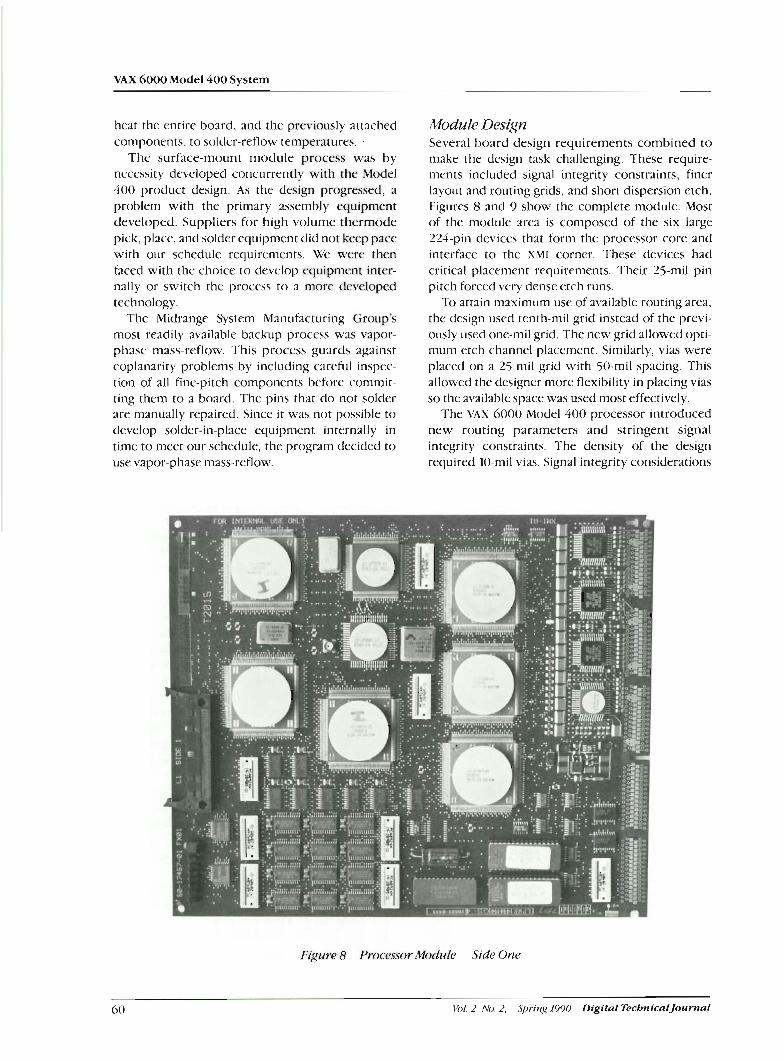
VAX 6000 Model 400 System
heat the entire board, and the previously attached components, to solder-reflow temperatures.
The surface-mount module process was by necessity developed concurrently with the Model 400 product design. As the design progressed, a problem with the primary assembly equipment developed. Suppliers for high-volume thermode pick, place, and solder equipment tlid not keep pace with our schedule req~iircments. We were then faced with the choice to dekclop cquipnlent inter- nally or switch the proccss to a more developed technology.
The Midrange System Manufacturing Group's most readily available backup process was vapor- phasc mass-reflow. This process guards against coplanarity problems by including carcfi~l inspec- tion of all fine-pitch components before commit- ting them to a board. The pins that do not solder are manually repaired. Since it was not possible to develop solder-in-place equipment internally in time to meet our schedule, the program decided to use vapor-phase mass-reflow
Module Design Several board design requirements combined to make the dcsign task challenging. These require- ments included signal integrity constraints, finer layout and routing grids, and short dispersion etch. Figures 8 and 9 show the complete module. Most of the module arca is composed of the six large 224-pin deviccs that form the processor core and interface to the XMI corner. These devices had critical placement requirements. Their 25-mil pin pitch forced very dense etch runs.
To attain maximum use of available routing area, the design used tenth-mil grid instead of the previ- ously used one-mil grid. The new grid allowed opti- mum etch channel placement. Similarly, vias were placed on a 25-mil grid with 50-mil spacing. This allowed the designer more flexibility in placing vias so the available space was used most effectively.
The vAx 6000 Model 400 processor introduced new routing parameters and stringent signal integrity constraints. The density of the design required 10-mil vias. Signal integrity considerations
Figure 8 Processor Mwlztle -Side One
60 Vol 2 IN. 2, Sprin,? 1990 Digital TecbntcalJournal

V M 6001) Model 400 Physical Technology
imposed component spacing and electrical connec- tion requirements that resulted in components being closer than suggested by current standards. Surface etch was needed to keep connections short. Components on side two were placed underneath fine-pitch devices on side one for electrical prox- imity. New manufacturability rules were generated to cover these situations as the design progressed.
Because surface layers are not used to route sig- nals, these layers were not designed to have good signal integrity characteristics. However, a signal has to travel a short distance from its pin p ~ d to its dispersion via which connects to an inner routing layer. Therefore, it is essential to keep surface etch as short as possible to minimize the distance the sig- nal travels outside a controlled impedance environ- ment. To meet this distance requirement, each critical component was placed very precisely and its dispersion pattern was individually designed.
Signal integrity considerations placed other con- straints on the design. Critical signals had to be kept
less than a specified maximum to meet perfor- mance specifications. To avoid skew problems, clocks were routed equal lengths to within a tight tolerance. Table 6 details the resulting design parameters.
Test Technology
Assembly and Test Process Development Assembly and test process issues were tracked throughout the development and selection of the Model 400 physical technology. The manufacturing impact of each physical technology choice was quantified in a spreadsheet analysis of cost and qual- ity metrics.
These metrics were estimated by using integrated assembly and test process models for each possible physical technology implementation. Two issues became evident during the physical technology selection process.
Figure 9 Processor Module -Side Two
Digital TechnicalJournal Vol 2 No. 2, 5pring 1990 6 1

VAX 6000 Model 400 System
Table 6 VAX 6000 Model 400 Processor Board Design Statistics
Parameter Value
General: Board size (inches) 9.2 x 11 .O
Board thickness (inches) .093 Layers 10 Initial route area (square inches) 99 Routing vias 1699 Dispersion vias 381 3 Total components 623 Total component pins 4976 Total used component pins 421 8 Total networks 1005 Total etch length (inches) 5002
First, the high number of signals and the fine pitch of those signals in all of the possible product implementations significantly increased the risk of manufacturing defects, such as shorts between signals or open faults along a signal. A continuity transistor structure (CTS) is designed into each of the VLsI (very large scale integration) devices to help test and diagnose these open faults.
Second, high-speed operation and reduced phys- ical access would make diagnosis of processor fail- ures difficult. To alleviate this problem, test features and a test system were developed. The test feature was a form of boundary scan, called observe boundary scan (OBS). The test system, the VAx 6000 Model 400 scan monitor, utilized the OBS in a system test environment.
Continuity Transislor Structure Because the devices are surface-mounted to the module, a large percentage of the manufacturing defects were expected to be open faults between the module and the chips. Typically, these open faults are difficult to detect and diagnose because they usually require the development of a set of complex test vectors that will be applied to the chip. To simpllfy the test for open faults, a continu- ity transistor structure (CTS) is designed into each chip. The CTS tests for open faults by using simple instruments such as voltage sources and current meters on an in-circuit tester (ICT).
The Module 400 CPU module is placed on a bed- of-nails f ~ ~ t u r e that gives the tester electrical access to at least one point on each internal module signal network. The tester then applies digital stimulus to
the internal module and verifies correct contact by reading current flow.
The CTS is shown in Figure 10. Pins 1 through N represent all signal pins on the chip. The design uses minimum-sized transistors. The CTS design does not require any dedicated pins because the test pin is a normal device signal pin. There is no perfor- mance penalty because the transistors are placed in parallel to the normal system logic, which results in a negligible load on those signals.
The use of the CTS in the processor module manufacturing process has been very successful. The ICT very quickly isolates open connections to the device pin and differentiates them from device test pattern failures. This process allows the open connection to be repaired rather than replacing the device.
Further, CTS testing allows prototype modules to be fully tested for assembly defects, even if the VLSI in-circuit test patterns are not available. This advantage is possible because designers can fully develop CTS tests without any knowledge of the VLSl device internal structure or function.
Observe Boundary Scan Modules that pass ICT testing are then tested at a "system like" test station. Self-tests and bootable diagnostics are run, and the VMS system is booted. If a module fails any of these tests, skilled technicians diagnose the failures by attaching logic analyzer probes to the module. Because of the fine-pitch surface-mount devices and the high-speed opera- tion, it is very difficult to attach logic analyzer probes to many nodes on the processor module.
OBS allows the CPU module to be observed as it executes VAX macrocode on board self-test stimu- lus at the module's full clock rate. This additional observation is used by the scan monitor to help test and diagnose module-level faults in a system test environment in stage-one manufacturing.
TEST PIN (ALSO A N O R M A L DEVICE SIGNAL PIN)
N-CHANNEL MOSFET
N-CHANNEL MOSFET -.. 6 :-ANNEL MOSFET
b PIN 1
Figure 10 Co~ztinuity Transistor Structure
Vol. 2 No. 2, Spring 1990 Digital TecbnicalJournal

V M 6000 Model 400 Pbpical Technology
Designing OBS into a custom VLSI device is more complex than adding CTS, but is still relatively sim- ple. OBS is simply a parallel-load, serial-shift register with one bit of the register on each device pin. Although it is not negligible, the OBS uses a rela- tively small amount of silicon area and also does not affect product performance. The total area used by both the CTS and OBS was estimated at about one to two percent of the chip area. Unlike CTS, which does not require any dedicated device pins, OBS uses two dedicated pins on each device in which i t is implemented. To fully utilize the OBS test fea- ture, the V.4X 6000 Model 400 scan monitor was designed and built.
The scan monitor controls and reads the OBS on the Model 400 module. A host computer system interfaces with the monitor. The scan monitor control program (sMCP) operates the scan monitor, makes passtfail decisions on the data received, and diagnoses failures. SMCP also includes many features that allow it to perform as a virtual logic analyzer, including waveform displays that high- light faulty behavior, as well as full triggering functionality.
Conclusion The aggressive performance goals and advanced semiconductor technology used for the VAX 6000 Model 400 processor meant a significant develop- ment effort for packaging and interconnect techno- logy. The technology requirements included high lead count, electrically tailored single-chip pack- ages, very dense controlled impedance printed wiring boards, a state-of-the-art surface-mount assembly process, and advanced test features.
The physical technology achievements in the VAX 6000 Model 400 project represent an effort in the packaging and interconnect disciplines more akin to mainframe and supercomputer develop- ments than to traditional microprocessor-based system approaches. The accomplishments of the efforts include:
Development and implementation of an advanced TAB technology for the high lead- count custom chips
Design of an innovative semicustomized ceramic single-chip package that combines the best fea- tures of surface-mount devices and traditional pin grid arrays
Development, sourcing, and qualification of very dense printed wiring boards with multiple controlled impedances
Achievement of a technology set capable of 28-11s clock cycles through the use of full elec- trical simulation at the device, package, and module levels
Development and implementation in manufac- turing of the SMT3 module assembly technology, which allows double-sided mounting, high lead-count fine-pitch surface mounting, surface- mounted passive components, and mixed com- ponent types
Introduction of innovative testability features, including the continuity transistor structure for assembly verification and observe boundary scan for diagnosis in engineering debug and module manufacturing
As intended at the outset of the project, these technologies will be employed on a significant num- ber of follow-on midrange and low-end products.
Acknowledgments A large number of people contributed to the success of the VAX 6000 Model 400 physical technology program. It is not possible to name all these impor- tant contributors in this space. Therefore, the authors want to acknowledge that the VAX 6000 Model 400 project could not have been undertaken nor have succeeded without significant efforts by members of the SCIT Physical Technology Group, Semiconductor Assembly Group, Midrange Systems Engneering Group, Corporate PWB Group, Mid- range Systems Integration Group, and the SClT Semiconductor Engineering Group.
Digital TecbnicalJorrrnal Vol. 2 No. 2, Spring 1990

Richard E. Calcagni Will Sherwood
VAX 6000 Model 400 CPU Chip Set Functional Design Verification
The VRY GOO0 Model 400 system is DQitulS Jirst VLSl CP (I to employ a fully micro- pipelined architecture. The CPU chip set for this system posed rmpcation challenges fur 6qan.d those of pwious designs. The major problem was the laqe tzumbw of complex: contml sequences and combinations that could exhibit design errors. A single uerrpcation strategy would not suJficient!y handle this comple,vTZ~~. 'I;berefore, z~criJication enginews developed a multipmged approach fmsimulution modeling and functional design verification. l B q 1 also emplo-yed CPU diagnostic programs, I~atd-generated tests, and directed pseudo-randm techniques to verif3, that the design conformed to the VAX architecture. These techniques helped them find bugs prior to committing the &ign to mush. As a result, theflrst-pass versions of the CPU chiy set s m f i u l l y booted an operating system. Simulation also minimized chip rework and delays in bringing theproduct to market.
m e Design Verification Project The VAX 6000 Model 400 chip set verification pro- ject had two goals: find implementation bugs in the design and verify that the design performed as a VAX
system. The design verification tasks involved about 25 person-years of effort in the areas of system microcode, custom VLSI (very large scale integra- tion) chips, and the VAX 6000 Model 400 scalar pro- cessor module.
The chip set verification team coordinated a set of simulation models originally written by the chip logic designers. At various stages of the project, models were available at the gateltransistor, behav- ioral, and architectural performance levels. The verification team used these models to run a wide assortment of both basic and sophisticated tests. The use of simulation models is described in more detail in the next section.
The CPU design was partitioned into functional units, and one or more units were assigned to each member of the verification team. A list of specific tests or testing activities w= produced for each sec- tion of the CPU chips' specifications. This list WAS
augmented by project-wide brainstorming sessions. These sessions were used to analyze obscure or sub- tle combinations of events in the design. Often, the thinking process would identify that a bug existed before any testing had been done. Verification engi-
neers used the list to create tests for the functional units of each chip. These tests were implemented in either microcode, macrocode, pin-stimulus, or somc combination of the three. Tests were imple- mented in the priority determined by the design team's identification of the most complex areas of the design and those most susceptible to bugs.
Simulation Models Functional design verification using software simu- lation is inherently slow in a design as large and complex as a VAX CPU.' To use resources most efficiently, the verification team specified and coor- dinated a project-wide modeling methodology that incorporated a number of different modeling levels, trading oft detail versus other factors such as speed. These trade-offs allowed us to match the testing of each phase of the design to a model that met its specific needs and characteristics. Thus, sirnula- tions were only as detailed as necessary for a parti- cular test situation, and the overall efficiency of the verification effort was increased. Most levels of modeling could contain different levels of descrip- tion detail for different areas of the design, which further optimized simulation performance.
There were three major phases of the design: architecture, detailed block diagram, and logic1
64 VoL 2 No. .% .Spring 1990 Digital TecbnicalJournal

Model 400 CPU Chip Set Functional Design Vmpcat ion
transistor schematic. To match these design levels, architectural, behavioral, and structural models were written. Each model section was written by its designer and then integrated into a whole-chip model, a system model, or both models for chip and system testing. In addition the design method ensured that the overall organization of each modeling level was Pdithful to the hardware design level i t represented.
Architectural Model The architectural-level model is the highest level of modeling for this project.'.',' This model describes only the control algorithms and abstract data paths in the microarchitecture. The VAX 6000 Model 400 C P u architects wrote this model in PASCAL for exe- cution performance reasons. The PASCAL program avoids most of the simulation-oriented overhead because it is a standalone program.
In the architectural model, actual microcode is used. However, because much of the detail of the microarchitecture is abstracted in this model, crutches (additional simulation aids) are required to execute the microcode flows. Model simulations are driven from instruction traces. Opcode, operand, and address information are extracted from user programs and system software running on actual VAX systems. Special fields in each microword make use of the information from these traces and direct the flow of microcode execution accordingly. These special fields are only used for simulation and are not included in the actual microcode implemented in hardware. The use of trace data extracted from real VAX systems permits actual machine loads to be reproduced, and the architect can evaluate implementation trade-offs from these reproductions.
Signals in the architectural model are correct to within a machine cycle, which allows execution times to be accurately measured. Microarchitec- tural parameters, such as cache or translation buffer size, can be easily adjusted to analyze their effects on system performance. More complex design fea- tures, such as bus protocols and pipeline control algorithms, can also be modified relatively easily.
The moclel describes most of the hardware sec- tions that will be in the final design. Therefore, it s e n e as a prototype system debugging tool to predict and tune system performance. The model also uncovers design flaws before implementation begins. About a hundred bugs were found at this preliminary stage by using the architectural model.
- - --
Digital TecbnicalJournal Vol 2 iVo. 2, .\pritig 1000
Behavioral Model The behavioral level model describes each chip sec- tion's logic in detail. It is written in the DECSIM behavioral modeling language.5."" DECSIM pro- vides a high-level computer-hardware description language that executes procedurally rather than using event-driven algorithms. Models written in such a language generally s i m p l ~ both model and design debugging.
The modeling methodology requires that, in the behavioral model, every signal in the design be explicitly modeled, with its timing accurate to the clock-phase boundary. This methodology maxi- mizes the probability that timing problems will be found at this level of simulation. (Note: N o addi- tional logic timing verification was done on this project.) Each designer writes the section's model in parallel with writing the chip's specification. The writing must be done before detailed schematics are started. This method ensures that the model accu- rately represents the real hardware behavior.
The model executes hierarchically. The system clocks are advanced at the begiming of each phase, then the top-level routines for each section are called. These routines, in turn, call the routines for each subsection. The subsection routines do the actual work.
The DECSIM behavioral model is the basis for many model variations. These variations range from the simplest single-CPU module to elaborate multi- processor versions that include peripherals and 110 adapters.
The basic version of the behavioral model is non- ported; i.e., the model is implemented as a single, self-contained hierarchy of procedures that does not use or connect to any other models. The non- ported model contains detailed descriptions of the three custom VLSl chips: CPU processor, secondary cache controller, and floating point accelerator. This model also includes a representation for backup cache RAMS connected to the DAL (data and address lines). Also modeled are a system support chip and a simple memory that can return data as fast as the protocol allows.
This nonported model was used for extensive testing of the microcode, microarchitecture, and logic design of the VLSI chips and their interf~ces. A majority of the verscation tests did not need detailed memory timing or 110. Tests could be run faster on the nonported model than on one that simulated the actual memory access delays. These delays would have increased the testing time with- out adding value to the testing process.

VAX GOO0 Model 400 System
Another version of the behavioral model is ported. This model was constructed to test the DAL and the interaction of the core chips with the system support chip (RSSC) and bus interface stan- dard cell (REXMI) chips."orted models have ports at the boundaries of procedural model compo- nents. Ports are used where chip pins or similar boundaries appear in the design. Ported model components are integrated for simulation through a structural wire list derived from module (printed wiring board) schematics. The main ported model consists of the core CPU chips with a ported repre- sentation of the DAL. This model connects to ported models of the other chips on the VAX 6000 Model 400 module, which in turn connect to memory and 110 models. Several different combinations of these ported models were used for various specific verification test applications as shown in Table 1. The combined ported models run several times slower than the less complex nonported model. The slower time is offset by increased testing granu- larity. The ported models also allow asynchronous
behavior, which in turn allows chip- and module- level interactions to be tested.
Table 1 lists more usages of the ported core chip set behavior model as compared to the nonported architectural performance model.
Structural Models The structural models were derived automatically from the designers' transistor-level schematics. The wirelists, or network descriptions, were translated for the two simulator systems: DECSIM MOS and the ZYCAD simulation engine."'"'." IIECSIM MOS is a transistor-level simulator based on RSIM and ESlM that models R-C delays, undefined-state initiali- zation, and charge I" The hardware- accelerated ZYCAD system abstracts transistors into a three-state, gate-level model. The DECSIM MOS model was used for standalone chip sections and whole chip simulations to find initialization and charge-sharing bugs. Both DECSIM MOS and ZYCAD were used to find logic and schematic bugs. Both systems used pin-level pattern stimulus that was
Table 1 Combinations of Behavioral Model Configurations
Performance Number of Module Number and Level (Microcycles/
Ported Modules Abstraction of Memory Peripherals Applications Second)
No 1 Architectural level; 1 Abstract memory None Architecture 600 per-cycle detail module debugging and
performance tuning
No 1 Behavioral level for 1 Abstract memory None CPU verification 7 support chips; per- module and generating phase detail chip test patterns
Yes 1 Behavioral level for 1 Detailed memory None Self-test code 2.5 support chips module debugging and
bus interface verification
Yes 2 Behavioral level for 2 Detailed memory None Multiprocessor 1 support chips modules verification
Yes 1 Behavioral support 1 Detailed memory 1 RL02 disk Booting V M S 2 chips module with gate- (high level) system
level bus interface Yes 1 Gate level for 1 Detailed memory None Bus interface 1
bus interface chips module with gate- verification and level bus interface generating chip
test patterns Yes 1 Gate level for 1 Detailed memory None Module 1
bus interface chips module with gate- verification level bus interface
Yes 2 Gate level for 2 Detailed memory Bus adapter System 0.5 bus interface chips modules with gate- verification in
level bus interface multiprocessor mode
66 Val. 2 No. 2, Spring 1930 Digital Technical Journal

%i?el400 CPU Chip Set Functional Design Vmpcation
generated from the nonported behavioral model. Signals traced in the behavioral model matched the boundary of the section of logic or chip being simulated at the gate level. Test results were com- pared on a cycle-by-cycle basis. The tests uncovered many bugs in the logic design implementation.
Gate-level Fault Simulation In addition to ZYCAD true-value simulation, single stuck-at fault simulation was done. Fault simulation measured verification and manufacturing test coverage, and provided guidance for verification engineers to enhance tests. The fault simulation effort for the CPU processor chip alone was almost six months long. As a result of this effort, five new tests were written, and manufacturing fault coverage was subsequently increased from 83 per- cent to 94 percent.
V ' f i c a t i o n Strategies CPU chip set verification engineers had two explicitly stated and somewhat overlapping goals. We had to prove that the hardware design intent adhered to the VAX architecture standard in every respect, and that the logic implementation adhered to the intent.15 We strongly believed that any bugs in prototype hardware (first-pass silicon for the custom VLSI chips) would negatively impact our ability to meet time-to-market for the product. Bugs found at a later stage of the design process are more expensive to fii for custom VLSI chips. It is expensive because we are severely restricted in our ability to isolate and work around bugs in the hard- ware. Therefore, for custom vLS1 chips, verification explicitly meant proving the design and finding the bugs in simulation. No single verification strategy or technique can find all of the bugs in something as complex as a VAX CPU. Therefore, a breadth of veri- fication strategies were flexibly applied.
In addition to technical strategies, the verifica- tion team cultivated a "bugs are good" philosophy throughout the project.'(' Past experience has shown us that bugs will always creep into the design of something as complex as a VAX CPU. Instead of being viewed as mistakes or failures, bugs were celebrated because a bug found in simulation was a bug that didn't make it into prototype hard- ware. This subtle shift in how the finding of a bug was regarded had, we believe, a strong motivational impact on members of the design and verification teams and increased the probability of finding bugs during verification.
Existing Design Verification Tests The VAx architecture has undergone a number of implementations since the first VAX-lli780 system was designed in the mid-1970s. Over the years, a substantial body of knowledge regarding the key areas and problems associated with designing a VAX
processor has been accumulated from various VAX implementations. We put these past lessons to use in the vAx 6000 Model 400 verification effort. We actively sought out bug lists, test plans, and actual test code used by previous VAX system design teams. One key example of this is HCORE, a self- checking VAX macrocoded diagnostic program. HCORE specifically focuses on the high-risk areas that are common across VAX designs. The HCORE test program was originally developed from another basic field-diagnostic program. It was Jater modified many times, throughout several projects, to focus on testing potential high-risk instructions and functional areas that had been identified in past designs. Existing design verification tests (DVT) such as this are almost always VAX macrocoded tests. Macrocoded tests transport more easily across implementations than microcoded tests because the microword formats are usually different from implementation to implementation.
We derived three benefits from using existing DVTs. They provided a strong level of confidence in the basic functional operation of the design. Sec- ond, they found any functional bugs that might be hiding in obscure or seldom used areas of the vAx instruction set. Third, when used with demons (explained later), they were usefill in finding bugs in very implementation-specific areas, such as error recovery logic.
Custam Design Verification Tests Although all vAX CPU designs implement the same architecture and run the same software, the hard- ware and firmware implementation details of each are unique. Therefore, generic VAX diagnostic tests did not necessarily cover the specific critical paths and functions in the VAX 6000 Model 400 design. Existing DVTs often could not provide a clear picture of what had and had not been covered. To solve these problems, we used custom DVTs to test specific, obscure, and hard-to-get-at areas of the design. There were several techniques for imple- menting custom DVTs:
Handwritten macrocode
Handwritten microcode
Digital TecbnicalJournal VoL 2 No. 2. Spring 1990 67

VAX 6000 Model 400 System
Manipulation of pins and internal signals under simulation control
These techniques could be used individually and in combination, within a single custom DVT. For example, although custom DvTs for the instruction fetch and parse logic (I-box) were written primarily in microcode, a custom macrocoded instruction stream was written to give the 1-box something to parse. Explicit manipulation of pins in simulation was used to generate asynchronous events, such as interrupts, when necessary.
Custom DvTs provided confidence in areas of the design that could not easily be tested with existing DVTs. We made the tests as focused and efficient as possible. However, in doing so, the generation of such tests required large amounts of development time and people resources. Although these tests uncovered several bugs in all areas of the design, we now believe that many of these same bugs could have been found with less labor-intensive methods, such as pseudo-random tests At the time, the pri- mary advantage of custom DVTs was the clear indication they gave that specific functional areas of the design had been tested and were working as specified.
Pseudo-random Design Vm!jiication Tests Each new \]AX CPU design aspires to improve on the price or performance of the previous design. Improvements are sought by pushing the limits of available technology to package hardware into smaller and, if possible, less expensive spaces. At the same time, a decrease in the cycle time or an increase in the work done per cycle in the func- tional design is also sought. In particular, this last item has substantially increased design complexity by introducing techniques such as pipelining and special-case hardware. As a result of this complex- ity, we often encounter very obscure bugs when debugging new VAX implementations. These bugs involve unanticipated interactions in the logic, between seemingly unrelated functional areas, and interactions dependent on intricate combinations and sequences of events. We were concerned about these types of bugs because it is extremely difficult to write tests for unanticipated problems. The method we chose to address these problems was pseudo-random testing.
The intent of pseudo-random testing is to exer- cise the design in ways that are likely to find bugs without necessarily knowing in advance what those bugs are or where they might be. Pseudo-random
testing implies simulating many cycles and trad- ing off test efficiency to address the problem of unanticipated bugs.
It is absolutely necessary to automate the pseudo- random test process, both test generation and test scoring, as much as possible since pseudo-random tests are much longer than focused tests.
A powerful tool already available for pseudo- random testing VAx designs is the \!Ax architectural exerciser tool suite (AXE and MAX)." Originally intended as hardware prototype verification tools, AXE and MAX have proven to be even more effec- tive as design verification tools in a simulation environment. They provide a virtually inex- haustible source of unique, interesting macrocode test cases, and require a minimum of intervention and effort by the user.
Although AXE and MAX provide some control over test case parameters, they still aspire to be gen- eral, architecturally focused exercisers. We also wanted pseudo-random test case generation that could be targeted at specific, risky areas of the implementation. These areas were the most likely locations for unanticipated bugs. Custom pseudo- random exercisers were developed for these areas. These exercisers provided very detailed control over test case parameters, yet retained many of the features and advantages of AXE and MAX.
A powerful techni ue for pseudo-random test is 1 4 the use of demons. A demon is any automated
intervention of a simulation model's normal execu- tion behavior. For example, a bus demon can inter- ject one or more bus commands, error conditions, or interrupts at random intervals in order to aggra- vate normal system operation. By doing this, a dense environment of unusual or uncommon event combinations can be created to stimulate the design with worst-case situations. Demons typically slowed model execution by a factor of ten, but they often found bugs that had not been considered by the designers or architects. Without demons, it could have taken many months of field testing to find and characterize these bugs, if they would have been found at all.
Pseudo-random testing with LYE, MAX, custom exercisers, and demons was used throughout the development cycle of the CpU chip set. All four uncovered obscure interaction bugs, as expected. Unfortunately, they did not find them all. Some unanticipated bugs slipped through verification and into the fist-pass silicon stage. These bugs were eventually found after running many more cycles in real prototype hardware. The failure to find all
Vol. 2 No. 2, Spring 1990 Digital Technical Journal

Model 400 CPU Ch@ Set Functional Design Verification
unanticipated bugs in the simulation stage illus- trates a fundamental problem in the use of pseudo- random testing. The effectiveness of testing is closely coupled to the number of cycles run, and simulation speed severely restricts this number.
Our application of pseudo-random testing to the problem of unanticipated bugs was largely success- ful for this project However, we learned that we must do more in the future to increase the efficiency and scope of these tests. To provide this increase, we are looklng toward more directed pseudo-random testing.
Booting the VMS Operating System A major milestone in thc development of any new VAX CPU is booting the vMS operating system on prototype hardware. Not only does this demon- strate significant functionality in the design, but it also provides a platform from which further testing can proceed. As previously stated, increased com- plexity in these designs can produce very subtle bugs. Often, such bugs do not even appear until the hardware is run under a heavy system load in a large multiprocessing or 110-intensive environment. Suc- cessfiilly booting VMS on prototype hardware is necessary before any such system load testing can begin. The sooner such testing begins, the better the chance of finding subtle bugs. For this reason, boot- ing the VMS system in simulation was an important goal of the VAX 6000 Model 400 chip development and verification effort.
At first glancc, it would seem impossible to boot the VMS system on a simulation model in a reason- able amount of time. Simulation speeds on the fastest of our models were many orders of magni- tude slower than actual hardware. However, careful analysis of the macrocode modules involved in the boot process revealed that by optimizing or remov- ing large, iterative sections of code, we could sub- stantially reduce thc number of cycles in the boot path without losing significant coverage for veri- fication. For example, the primary bootstrap mod- ule contains code that creates a bit map of all physical memory in the system. The code tests each memory location for errors. By reducing this code to test fewer memory locations, the number of cycles executed is vastly reduced.
Another key optimization involved speeding up simulated transfers from disk. At several points dur- ing the boot process, code and data are pulled into memory from a mass storage device (usually a disk). For simulation, a special "turbo" disk model was written by the verification team. This model arti-
Digital TecbnicalJournal Vol. 2 No. 2, Spring 1990
ficially processes model requests for block data transfers and performs the transfers instantly. This technique eliminated wasting simulated CPU cycles while waiting for transfers to complete.
With model and code optimizations in place, booting the ms system to the point of printing the VMS banner and starting the process scheduler was actually achieved in simulation. It took approxi- mately seven CPU days on a host VLY 8800 system. One model bug and one real design bug were found during this effort. Booting the ViMs system in simu- lation required a large amount of verification resources. The process was worthwhile in terms of the bugs that were found and the confidence it gave us that we could boot v M S on first-pass hardware.
Analysis of tbe Functional Bugs Found To demonstrate where the verification project was successful and where it needed improvement, we discuss here the bugs that were found both before and after the chip set fist-pass design was commit- ted to masks. (Note: The milestone of this commit- ment is called PC, for mask data preparation's pattern generation.) Only the bugs pertaining to architecture, microcode, functional design, and logic design are discussed. Layout and circuit prob- lems, as well as modeling and tool bugs, are outside the scope of this paper.
During the design period, several hundred bugs, with a variety of complexity levels, were found in all sections of the design. These bugs were found through the verification techniques described in previous sections and are detailed in Table 2.
The prototype chips were first tested on a Takeda 3381 chip tester. This tester allowed prototype chips to be tested in a standalone environment. The chips were then inserted into a prototype CPU module, which was part of a custom-designed engi- neering tester. The prototype module provided a
Table 2 Methods Used to Find Design Bugs before F i r s t - ~ a ~ S Silicon
Number of Verification Process Bugs Found
Custom DVTs, DVT reviews, microcode assertions Existing macrocode test programs Pseudo-random macrocode tests Boot V M S operating system on the behavioral model Total of bugs found prior to first-pass silicon
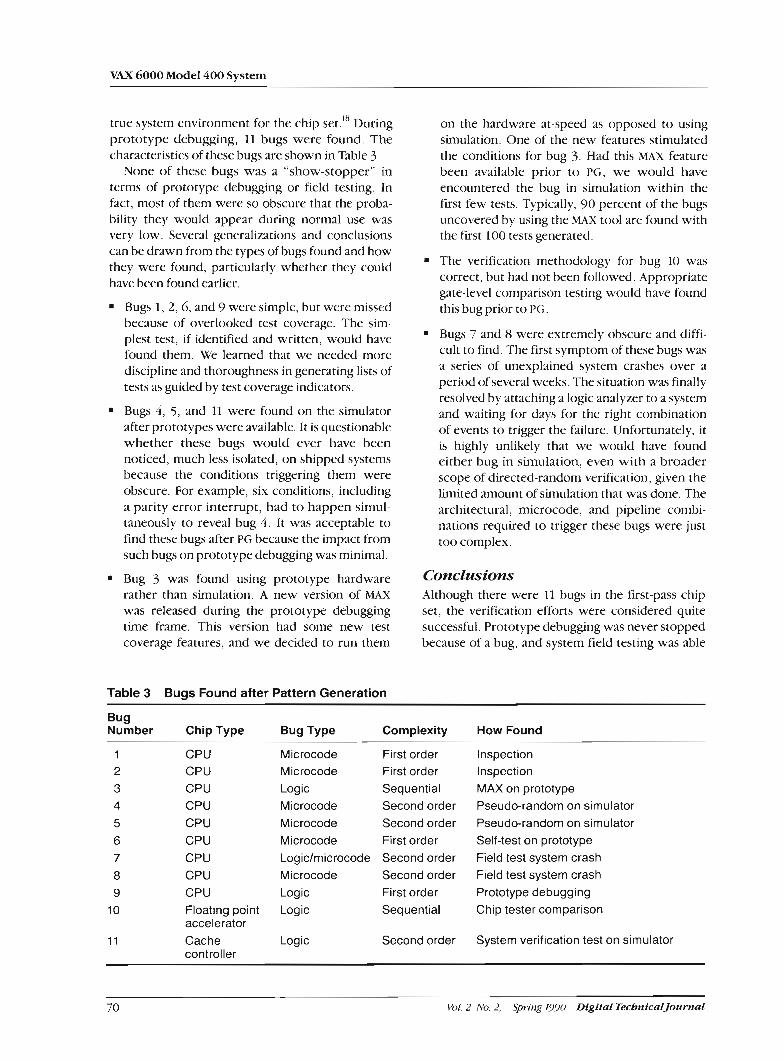
VAX 6000 Model 400 System
true system environment for the chip set." During prototype debugging, 11 bugs n7ere found. The characteristics of these bugs are shown in Table 3.
None of these bugs was a "show-stopper" in terms of prototype debugging or field testing. In fact, most of them were so obscure that the proba- bility they would appear during normal use was very low. Several generalizations and conclusions can be drawn from the types of bugs found and how they were found, particularly whether they could have been found earlier.
Bugs 1, 2,6, and 9 were simple, but were missed because of overlooked test coverage. The sim- plest test, if identified and written, would have found them. We learned that we needed more discipline and thoroughness in generating lists of tests as guided by test coverage indicators.
Bugs 4, 5, and 11 were found on the simulator after prototypes were available. It is questionable whether these bugs would ever have been noticed, much less isolated, on shipped systems because the conditions triggering them were obscure. For example, six conditions, including a parity error interrupt, had to happen simul- taneously to reveal bug 4 . It was acceptable to find these bugs after PG because the impact from such bugs on prototype debugging was minimal.
on the hardware at-speed as opposed to using simulation. One of the new features stimulated the conditions for bug 3. Had this MAX feature been available prior to PC, we would have encountered the bug in simulation within the first few tests. Typically, 90 percent of the bugs uncovered by using the MAX tool are found with the first 100 tests generated.
The verification methodology for bug 10 was correct, but had not been followed. Appropriate gate-level comparison testing would have found this bug prior to PC.
Bugs 7 and 8 were extremely obscure and diffi- cult to find. The first symptom of these bugs was a series of unexplained system crashes over a period of several weeks. The situation was finally resolved by attaching a logic analyzer to a system and waiting for days for the right combination of events to trigger the failure. Unfortunately, it is highly unlikely that we would have found either bug in simulation, even with a broader scope of directed-random verification, given the limited amount of simulation that was done. The architectural, microcode, and pipeline combi- nations required to trigger these bugs were just too complex.
Bug 3 was found using prototype hardware C O Y U : ~ J S ~ ~ rather than simulation. A new version of MAX Although there were 11 bugs in the fist-pass chip was released during the prototype debugging set, the verification efforts were considered quite time frame. This version had some new test successful. Prototype debugging was never stopped coverage features, and we decided to run them because of a bug, and system field testing was able
Table 3 Bugs Found after Pattern Generation
Bug Number Chip Type Bug Type Complexity How Found
1 CPU Microcode First order Inspection 2 CPU Microcode First order Inspection 3 CPU Logic Sequential MAX on prototype 4 CPU Microcode Second order Pseudo-random on simulator 5 CPU Microcode Second order Pseudo-random on simulator 6 CPU Microcode First order Self-test on prototype 7 CPU Logiclmicrocode Second order Field test system crash 8 CPU Microcode Second order Field test system crash 9 CPU Logic First order Prototype debugging
10 Floating point Logic Sequential Chip tester comparison accelerator
11 Cache Logic Second order System verification test on simulator controller
70 1/01, 2 No. 2, 5$ring 1990 Digital TecbnicalJournal

?del400 CPU Chz9 Set Functional Design Vmfication
to complete on schedule. The modeling and veri- fication methodologies contributed to this success.
All logic, functional, and microcode bugs could be reproduced in the behavioral model. There- fore, the bugs found after % could have been found with simulation had the appropriate com- bination of events been tested.
Complex pipeline activity, an area of concern from the beginning, was the primary problem area in the design. Compromising design com- plexity to make thorough verification more achievable should be considered.
In general, the tool or test that first exercised a chip section or functional area with a bug found the bug. We believe this indicates that it is more productive to first debug using existing macrocode tests or automatically generated tests before writing new tests.
Although the effort to boot the VMS operating system on the simulator was comparatively large, one bug was found that would not have been found through other means. We had not considered the combination of events that caused the bug. Finding this bug clearly showed the benefit of running this application on the simulator. Further, it gave us confidence that the VMS operating system would boot on the first- pass prototype hardware to ensure that proto- type debugging could proceed unimpeded.
The flexible and wide-ranging modeling meth- odology served the design team well. The source code of the CPU chip set model has been reused in system verification and chip set application development projects at least ten times. The cor- porate standard DECSIM logic simulator made this modeling effort savings possible.
Acknowledgments The verification of the CPU chip set design was a team effort performed by the Semiconductor Engineering Group's microprocessor verification team. Members of this team included David Asher, Rick Calcagni, Liza Hudepohl, George Mills, Rick Pekkala, Ed Rocha, Will Sherwood, and Chris Spear. Part of our success is attributed to our CAD tool development groups, including the SEGCAD DECSIM team and the VAx Architecture Group AXE1 lMAX team. We would also like to thank Mike Uhler for his technical guidance throughout the project.
References
1. J. Basmaji et al., "The Role of Computer-aided Engineering in the Design of the VAx 6200 System ," Digital Technical Journal, vol. 1 , no. 7 (August 1988): 47-56.
2. C. Wiecek, "The Simulation of Processor Performance for the VAX 8800 Family," Digital Technical Journal, vol. 1 , no. 4 (February 1987): 100-110.
3. C. Wiecek and S. Steely, "Performance Simu- lation as a Tool in Central Processing Unit Design," Perfomnce Evaluation Review, vol. 11, no. 1 (August 1979): 41-47.
4 . B. Moses and K. DeGregory, "Performance Evaluation of the VAx 6200 Systems," Digital TechicalJournal, vol. 1, no. 7 (August 1988): 64-78.
5. M. Kearney, "DECSIM: A Multilevel Simulation System for Digital Design," Proceedings of ICCAD (October 1984).
6. R. Gries and J. Woodward, "Software Tools Used in the Development of a VLSI vAX
Microcomputer," Proceedings of the MICRO-17 Conferme (October 1984).
7. W. Sherwood, "An Interactive Simulation Debugging Interface," Computer Hardware Description Languages and Tbeir Appli- cations, Breuer and Hartenstein, editors, (Amsterdam: North-Holland Publishing, 1981): 137-144.
8. P. Sullivan et al., "The VAX 6000 Model 400 Scalar Processor Module," Digital Technical Journal, vol. 2, no. 2 (Spring 1990, this issue): 27-35.
9. B. Milne, "Put the Pedal to the Metal with Simu- lation Accelerators," Electronic Design, vol. 35, no. 21 (September 1987): 39-52.
M. McMahon, "Accelerators for Faster Logic Simulation: The ZYCAD Approach," Proceed- ings of VLSI and Computers, First Interna- tional Conference on Computer Technology, Systems and Applications (COMPEURO '87 Cat. NO. 8 7 ~ ~ 2 4 1 7 - 4 , 1987): 981.
11. D. Jenkins and S. Morton, "Transistor-Level Logic Simulation Using the ZYCAD Logic Evaluator," Proceedings of the Conference on Automated Design and Engineering for Electronics (1985): 154-163.
Digital TechnicalJournal VoL 2 No. 2, SLn-ing 1990 7 1

VAX 6000 Model 400 System
12. C. Terman, "Timing Simulation for Large Digital MOS Circuits," Computer-aided Design of VLSI Circuits and S ' m , ((Greenwich: JAI Press, 1986).
13. C. Terman, "RSIM-A Logic-Level Timing Simulator," International Conference on Computers and Design ( 1983).
14. C. Terman, "Simulation Tools for Digital LSl Design ," Technical Report TR- 304, M ITILCS (Cambridge: MIT Laboratory for Computer Science, 1983).
15. T. Leonard, ed., VAX Architecture Reference Mantlal (Bedford: Digital Press, Order No. E Y - ~ ~ ~ ~ E - D P , 1987).
16. D. Clark, "Bugs are Good: A Problem-oriented Approach to the Management of Design Engi- neering," Research - Technology Management (forthcoming 1990).
17. D. Rhandarkar, "Architecture Management for Ensuring Software Compatibility in the VAX Family of Computers," IEEE Cmputer (February 1982): 87-93.
18. W. Sherwood, "The VLSI VAX Chip Set Micro- architecture," Microarchitecture of VLSI C m - puters, P. Antognetti, ed. (1985): 103-126.
72 Wl. 2 No. 2, Sp'r'ng 1990 Digital TecbnkalJorrnal

John W Croll Larry T. Camilli
Anthony J. Vmcaro
Test and Qualification of the V M 6000 Model 400 System
Computer-aided design simulation, u~hich is used in the design of the VAX 6000 family, finds most problem during the hardware design phase. Simulation, however, cannot test a cmnpkx systenz running under system softu~are control. For the VRY (jOO0 model 400 system, a qualification process was designed to coml~letely test the interaction of the system S hardware and soflware components. The benefit of such a process is clearly shown in the results. Nearly all the problems found in the qualification stage could not have been found in the simulation process. me testing and qual$ication of the Model 400 was a multigrotlp eflort. This paper desmMbes the metho& and tools of three Midrange Systems Engineering groups who were involved in theproject.
The VAX 6000 Model 400 system is the third in the v A X 6000 series. The Model 400 is designed to enhance CPU performance using the same platform, that is cabinetry, buses, and power systems, as all moclels in the VAX 6000 family. The basic architec- ture of the VAX 6000 Model 400 is unchanged from that of the earlier Model 200 and 300 systems.'.',' The Modcl 400 is distinguished from earlier models primarily by two additions: a new processor design, which offers over twice the performance of the original VAX 6000 Model 200 processor, and by the addition of a vector coprocessor."5 The interfaces in the Model 400 to the common platform remain the same. However, the processor is an entirely new design, and is the first Digital system to use semi- conductors designed with the CMOS-2 process."
All VAX 6000 systems use a common design pro- cess that relies heavily upon simulation to detect and correct design errors. This simulation process is designed to ensure that first-pass hardware, or the initial engineering prototypes, will run the operat- ing system at speed.- The VAX 6000 Model 400 processor is an excellent example of the effec- tiveness of simulation techniques. The elapsed time from power-on of the first prototype to reliable login under both the ViMS and [JLTKlX operating systems was less than six weeks, which is sub- stantially less time than has been seen for previous v ~ x processors.
Current computer systems are very complex, especially when hardware and software interac- tions are considcred. Simulation cannot adequately
test hardware executing under operating system control. A companion system test and qualification process, executed on hardware prototypes, is required to thoroughly test the complete system and ensure its reliability.
A key goal of the \!Ax 6000 common-platform design strategy was to allow new processor tech- nology to be brought to the market quickly. To achieve this goal, we had to minimize the time required for system test and qualification without compromising the quality or reliability of the final product. By reusing common platform compo- nents, we could primarily focus on testing the new components.
This paper addresses the system test and qual- ification process used for the VAX 6000 Model 400 system. This process was designed to maximize test effectiveness and minimize test time. The fist cus- tomcr shipments of the VAX 6000 Model 400 system occurred only six months after the introduction of its predecessor, the \!AX 6000 Model 300 system.
System Test and ~ l i f i i c a t i o n Process The VAX 6000 Model 400 System Integration Group is responsible for the overall design ancl manage- ment of the system test and qualification process. This group comprises engineers who reside within the hardware design group, but havc not directly participated in the design of the components being tested. Therefore. any problems found during the test period can be rapidly communicated and resolved, whereas the possibility of "testing to
Digital TecbnicalJournal Vol. 2 I V ~ . 2, Sprit~g 1990 7 3

VAX 6000 Model 400 System
implementation" versus "testing to specification" is avoided.
A distributed test process was developed for the VAX 6000 Model 400 system that used the resources and expertise of a variety of groups within Digital. The test process also allowed many tcsts to be cxe- cuted in parallel to minimize time. Additionally, some of these groups have specialized test Facilities that are required to satisfy standards imposed by Digital and various government regulatory bodies, e.g., the FCC and UL.
The groups that participated in testing the Viuc 6000 Model 400 system, together with a brief description of each group's function, are shown in Table 1. Each group played a valuable role in testing a particular aspect of the system. Initially, a very aggressive test schedule of six months for the entire test and qualification process was planned. How- ever, due to some delays in planned prototype availability, all testing had to be completed in about five months to allow systems to ship as scheduled in July 1989. The expertise of all the groups involved was recluired to meet this schedule. However, space
limitations prohibit an in-depth discussion of each function. Therefore, we will examine in-depth the roles of three of the Midrange Systems Engineering Groups- the VAX 6000 Model 400 System Integra- tion Group; the VAX Architecture Verification Group; and the Midrange Systems Evaluation Engi- neering Group. We will also describe the tests and tools used in the qualification of the vAX 6000 Model 400 system.
System Integration Group Planning for the system test and qualification of the Vtuc 6000 Model 400 system began approximately one year prior to scheduled availability of the first prototype systems. During this period, the overall qualification plan was developed, and individual test plans were solicited from each group that would participate in the testing. Each plan was reviewed by the System Integration Group for test coverage, as well as for minimization of overlaps and duplication in the component plans. In parallel, the System lntegration Group developed plans for hardware-specific system design verification tests
Table 1 Organizations Involved in System Qualification
Organization Function
System Integration
VAX System Architecture Midrange Systems Evaluation Engineering VAXcluster Validation
Mechanical Technology
Electromagnetic Compatibility Engineering Product Safety Laboratory
Diagnostic Quality Assurance Manufacturing Product Verification Central Characterization Group
System Performance Analysis Group Customer Services Systems Engineering Software Quality Maintenance
Systems Reliability Engineering
Manage qualification process; perform DVT, system test, reliability confidence test; manage field test Exercise new system to find discrepancies with the VAX architecture Test a variety of system configurations for proper operation, concentrating on 110 configurations Test complex VAXcluster environments with new products to find problems in new or existing VAXcluster components Demonstrate successful product operation while exposed to specific environmental conditions (e.g., vibration, humidity, altitude) Test new products for electromagnetic compliance to various government regulatory requirements (e.g., FCC, VDE) Test various aspects of new product safety and ensure compliance to safety standards (e.g., UL, CSA) Test various diagnostic programs to ensure correct operation Provide the necessary data to verify and improve the manufacturing process to enable consistent production of a quality product Characterize performance of industry and application-specific workloads Model and measure performance of midrange products
Develop service delivery and training programs, test diagnostic and repair features of products Test software-layered product operability with new hardware and operating system versions Predict, test, and analyze hardware and system reliability
74 Vol. 2 No. 2, Spring 1990 Digital TecbnicalJournal

Test and Qmlzjication of the VHX 6000 Model 400 System
(DVTs) and for external field test. Prototype plans specified the number, distribution, and cost of the prototyped systems that would be required during the test period.
The System Integration Group also acted as the problem-reporting center. In implementing a dis- tributed test process, two functions are essential. There must be a central focus that disseminates information regarding observed problems to all test groups. Second, an established method for tracking status and resolution of these problems must be maintained. An internally designed system maintained a complete audit history of each prob- lem. There were 121 problems reported during VAx 6000 Model 400 testing. Each step in the reso- iution process was tracked for each problem in the problem database. This database was available to all test groups. The database was supplemented by weekly cross-functional meetings, at which repre- sentatives from engineering, manufacturing, and customer services reviewed and updated each problem's status.
The complex VAX 6000 Model 400 project sched- ule was developed and tracked by the group. Due to the number of groups involved in testing and the delays involved when problems were found, the critical path tended to be very dynamic during the test phase. A project management tool, which was developed within Digital and which used PERT, tracked status against milestones and modeled dif- ferent scenarios to prevent overall schedule slip- page as changes occurred.
The System Integration Group performed four major types of test. These were system test, reli- ability confidence test, design verification tests, and field test The following sections describe each of these tests.
S'tem Test There are two forms of system testing, directed and random. Most testing groups use directed tests, which test hardware or software features, or follow a strict test sequence. Directed tests seek specific results and are well defined.
The System Integration Group performed many directed tests on the Model 400 system. Some of these tests were done to satisfy the requirements of external regulatory agencies, or internal Digital development standards. Other directed tests include system DVT tests, which are discussed in more detail later in this paper.
Many aspects of complex systems cannot be ade- quately tested in a directed fashion. For example,
an operating system and a processor can operate in a nearly infinite number of states. It is impossible to design a series of tests to verify each of these states.
Random tests exercise the system in more com- prehensive ways than directed tests. They do not seek specific results. Instead, random tests attempt to push the system into as many different states as possible, as quickly as possible. Greater test cover- age results from these tests, hut problem diagnosis and isolation are more difficult.
Because random testing does not look for specific results, it is effective only if done for extended periods of time Even if identical test scripts are run repeatedly, system activity becomes unpredictable over time, due to events such as network activity or disk fragmentation. This unpredictability is impor- tant because it means more system states are being exercised.
The System Integration Group developed a ran- dom test package, called the Systems Integration Test Package (SITP), to test the VAX 6000 Model 400 system. This package consists of a comprehensive collection of test programs and a script-driven mechanism that controls their execution. SlTP is diverse and flexible. The test programs were obtained from many sources. The System Integra- tion Group also wrote some test programs to exer- cise specific aspects of the Model 400 system that were not fully exercised by other tests.
The test programs used with SlTP are high level. Each high-level test uses many lower level functions within the system. Many of these programs are run together, with varying test parameters and run- times. The programs are self-checking. If an action does not complete properly, the program notes the error immediately. The program does not attempt to identlfy the cause of an error; rather, it gathers as much information about the error as possible. This information is later examined by a test engineer.
SlTP is easy to use, restarts automatically after system crashes or power failures, and includes mon- itoring tools. Periodic reports, with deta~ls about system activity and error log data, are generated by the test package. With this information, the test engineer can gauge the effectiveness of the tests and adjust them as necessary. The test engineer can also control and monitor tests on many different machines. Machines can be located locally and remotely.
A number of srTP scripts were developed to provide different workloads for testing the Model 400 system. Each set of scripts emphasized a dif- ferent type of system activity. Some were com-

VAX 6000 Model 400 System
pute intensive, some 1 1 0 intensive, and some stressed parallel and multiprocessing activity. The scripts were modified to suit systcm configurations as needed.
SITP and the test scripts were installed on all the Model 400 system prototypes in the system integra- tion lab. Tests under the control of SITP were run on the prototypes as prototypes were available. Because the prototypes were heavily used during daytime hours for various debugging tasks, sITP tests were run overnight and on weckcnds. l'he test scripts were designed to run for a specific number of hours and then stop. The prototype was then available for the next user. This procedure allowed otherwise idle prototype hours to be used in system testing and ensured a clean shutdown of the tests. In this way, test data could be retrieved without inter- ference from other prototype users.
SITP was used on the earliest Model 400 system prototypes and was continually uscd throughout the qualification period, as prototype time was available. Scripts werc tailored to cause test con- centration in specific areas and were modified as necessary to suit various prototype configurations. Typical SITP runs would last for 16 or 19 hours (overnight), or 58 or 60 hours (over weekends). Processor, memory, and 110 configurations varied from run to run, and depended on test nceds and equipment availability.
The overall results from system testing were very positive. Over 6700 CPu hours were accumulated on various prototypes and configurations. Many errors were encountered during this period, but most were due to SlTP bugs (SITP was still under development for most of this period) or to errors in setting up test scripts. Hardware errors occurred in peripheral devices, principally disks and com- munications devices, and were corrected as they occurred.
Of the more serious problems found, one was a hardware problem that would cause a system hang. The problem was identified as a bug in a bus inter- face chip on the CPu module, which was operating in an untested mode. It was resolved by mod~fying the system console to ensure that this mode was never used. An error was found in the VMS machine check handler, which was corrected in a subse- quent release of the VMS operating system.
Five other serious bugs were found in the new CI'U modules. Although none of these bugs were found by the System Integration Croup's testing, each took time to investigate, resolve, and test the fixes. As a result, there was less time available on
prototype machines for other testing. Two of these bugs were fixed by modifications to the C p u mod- ule. The other three required changes to the proces- sor chip. As corrected processor chips became available, SITJ' was used to ensure the fvtes had not introduced further bugs.
It is interesting to note that four of these five problems occurred in system areas not simulated during hardware design. Of these four, two occurred in the handling of external system events. One was in system reset handling. The other was in handling "control/P" interrupts. ControlIP is the standard method an operator uses to get the atten- tion of the system console on VAX systems.' Two bugs were caused by interactions between the new processor and other system components. These interactions were not simulated during hardware design. The fifth bug was not found during sirnula- tion because of a deficiency in a simulation test tool.
Reliability Confidence Test To accumulate uninterrupted run-time on the Model 400 system, five identically configured sys- tems were set up in an isolated area. The machines were isolated to protect them from outside inter- ference while the confidence test was running.
The purpose of this test was to determine the actual reliability parameters of the Model 400 system hardware and to compare the results to the system's actual reliability requirements. A second- ary goal of the test was to determine the long-term system reliability, both for the hardware and oper- ating system software.
The duration of the test was planned for six weeks, which was sufficient to show the hardware reliability. Once this six-week period was over, we planned to continue to run the machines in the same environment with the same workload for as long as possible to accumulate further system run-time.
The test started at the beginning of May 1989, when enough CPU modules became available to populate the five machines. The formal test period ended two months later, in late June. Three of the machines continued to run for two and a half months, until mid-September. Of the other two machines, one machine was needed for other pur- poses, and another's CpU modules were removed to change the configurations of the remaining three.
The systems ran identical SITP scripts that con- centrated on exercising the new CPUs. Tests included compute-intensive programs, programs that explicitly tested various aspects of the new
Vol. 2 No. 2 Spring 1990 Digital TecbnicalJournal

Test and Qualification of the VAX GOO0 Model 400 System
CPUs (e.g., multiprocessor cache coherency), some decomposed parallel applications, and tests that generated many VMS processes.
The overall results of these tests were very good. The systems demonstrated a hardware reliability of over a year between hardware failures.
Only two module failures occurred. One had a bad cache tag store, which was discovered very early in the test. As a result of this discovery, the test process for the CPU module's cache control chip was changed. The other module failure was a float- ing point chip failure. One specific test program began generating wrong answers late in the formal period of the confidence test. This module was removed for repair.
Of the other failures that occurred during this test, all were attributable either to test script or set-up errors, o r to software or hardware prob- lems which were corrected prior to shipment to customers.
Once the formal test period was completed, the three machines that continued to run until mid- September exhibited no new failures and eventu- ally accumulated a year's run-time. The reliability of the VAX 6000 platform and the Model 400 CPU was successfully demonstrated.
Design Verification Tests Part of the System Integration Group's responsibil- ity is to ensure that parts of the system not covered by tests from other groups are tested. In general, these parts are specific either to the new hardware
or to how the new hardware fits into the existing system. These tests are called design verification tests (DVTS).
A complete test plan for the Model 400 system DVTs was written and reviewed by the group. The list of DVTs performed is shown in Table 2.
The Model 400 DVTs complemented those tests performed on the new hardware components. The parts of the system tested were those in which other testing was weak or nonexistent. These tests were conducted in a formal manner, with a written sequence of events and formal reports of results. Any problems found were noted and reported to the relevant development groups for analysis and eventual correction.
The DVTs executed for the Model 400 uncovered two system bugs and some minor documentation problems. Both bugs were related to power failure recovery. One was in the console and one in the VMS operating system. Both bugs were eventually fiixed. The minor documentation problems in the system installation guide were also fixed. All other design verification tests found no problems with the system.
Field Test Field tests are made on prototypes of new products provided to customers. The purpose of field test is to gain experience with the new products before production; new products are actually used as opposed to tested.
Table 2 VAX 6000 Model 400 System Design Verification Tests
Test Function
Keyswitch Voltage margin Thermal Power-faillbattery backup Interlocks XMI saturation Queue contention Multiprocessing Load test System installation Boot System configuration Remote services console
Console input
Verifies front panel functions with new hardwarelsoftware Verifies proper operation over allowable voltage range Verifies proper operation over allowable temperature range Tests battery backup operation with hardware and software Tests memory interlock functions Tests system operation under very heavy bus loads Tests proper operation under very heavy worst-case memory loads Tests proper operation of all multiprocessing features Runs system for extended period under heavy compute and 110 load Verifies overall manufacturing process, and installation documentation Verifies that system boots all operating systems from all devices Verifies that all allowable configurations work properly Verifies that remote services console hardware and process works with new system Verifies that console terminal hardware and software work properly
Digital TechicalJournal Vol. 2 No. 2 Spring 1990 77

VAX 6000 Model 400 System
For VAX system products, field test historically has lasted a minimum of four months. This period was determined from tracking problem reports from field test sites. Generally, a month was required for the new product to be installed and for usage to reach a level where meaningful testing occurred. The next three months provided useful data about the new system. After three months, the amount of useful data declined.
In field testing the VAX 6000 Model 400 system, we shortened this four-month period to three. The plan was to check on field test results two months into the test. If field test was not progressing well at this point, we were prepared to extend the test period.
The System Integration Group did two things to eliminate the field test startup time. First, because the Model 400 system n7as an upgrade from earlier VAX 6000 systems, Model 200 systems were shipped to each field test site in advance of the Model 400 field test start. These systems were installed and running approximately a wcck before the official field test started. A considerable amount of time was saved in site preparation and system installation.
Second, the startup of the field test sites was performed by system integration engineers, who brought Model 400 CPU modules and new VMS software to each site. These engineers supervised the installation of the new CPI's in the previously installed systems, installed the VMS operating sys- tem, and ensured that the systems were available to the customer before leaving the site.
A total of seven field test sites were started up in early April 1989. Six of these sites were located in the United States. Five of these sites were installed and turned over to the customers within two days. The sixth site nlas ready in four days. The seventh site was located in Europe, and was started up by mid-April.
Once the site systems were running, the System Integration Group maintained regular contact with each site. Each site was assigned a "captain" (a sys- tem integration engineer), who polled the site weekly, talked to the users, and received first-hand information about machine usage. This method was used instead of the traditional dial-up problem reporting method for two reasons. First, technical problems existed in making reliable connection to the dial-up system. Second, many people are reluc- tant to report problems, unless the problem is so large that work stops or is severely impaired.
Overall, field test went smoothly. Most of the problems that occurred were minor and easily cor-
rected. Two problems arose because the Model400 system was different from the other VAX systems in use at two of the sites. One site reported minor dif- ferences in results from a benchmark program, which was due to differences between run-time libraries used for full VAX architecture implementa- tions and subset implementations,x The other prob- lem resulted because a customer program was referencing an internal processor register that does not exist in subset implementations.
Field test progress was assessed two months into the test, at the beginning ofJune. The results of field test were then examined, together with the data obtained from other qualification testing. Since no major problems had been found, we decided to pro- ceed with plans to ship the Model 400 system ns scheduled in mid-July.
Some improvements could have been made in the field test process. First, site audits prior to instal- lation of the prototypes were not very thorough. Many of the sites were not running the neces- sary software revision levels. Therefore, the new machines could not be immediately put into VAXcluster environments with existing machines. Second, some pieces of hardware were missing and had to be supplied later. Better communications with the site prior to shipping prototypes would have reduced these problems.
The System Integration Group wrote some moni- toring software that was to be installed on each field test machine. Because this was written at the last minute, it was not properly tested and did not work properly. The problems were fixed, but the moni- toring software was not nin at all the sites. Finally, how to get data from the monitoring software back to the engineering groups was not well defined. Thus, usage data obtained from field test machines was spotty. These tools and methods are being improved for use in the field test of future products.
VAX Architecture Vmyication Group The Architecture Verification Group ensured that the Model 400 CrU conformed to the VAX architec- ture specification.'
Test Process Overview The architectural verification process consists of running two programs- AXE (architecture exer- ciser) and MAX (multi-instruction architecture exerciser)- in various modes for a given number of test cases. The tests are simple to run. However, the test programs are quite complex and required many years to develop. The Architecture Verification
k t . 2 No. 2, Spring 1990 Dfgllal TecbnicalJouml

Test and Qualifcation of the V M GO00 Model 400 System
Group maintains and enhances these test programs and the databases used to verify the architecture.
When one of the tests fails, the group identifies the problem and helps resolve i t . Once the problem is fmed, the group repeats the tests.
AXE and MAX The \/AX instruction set consists of over 360 instruc- tions and 21 addressing modes. Most modes are valid for up to six operands per instruction. Con- ceptually, both AXE and MAX divide an instruction's context into several components. These com- ponents include opcode, operand specifiers, oper- ands, page protection and validity, and processor status long word (PSL). For each component, valid and invalid values are pseudo-randomly selected to create a test case. The exerciser continues to create unique cases for as long as it is run.
The VAX architecture has a clearly defined excep- tion and instruction restart structure. Much of the VAX architecture's complexity is in those opera- tions. Therefore, both AXE and MAX favor values that cause faults. Each program establishes a situa- tion with faults, starts the instruction or sequence, verifies that the fault occurs, fixes the fault, restarts the instruction, and verifies that it completes cor- rectl y. Upon completion, AXE or m compares the results from the unit under test to a known good reference, and reports any differences. The known good references contain the correct results of each test case. These references have been accumulated over the years of testing VAX systems and have changed as the VAX architecture changed.
AXE AXE is the older and simpler exerciser. It cre- ates test cases that consist of a single instruction. A typical instruction stream would be:
When this instruction is first executed, either a resewed operand fault (on R1) or a resewed addressing mode fault (short literal destination) should be reported. AXE will fix whichever fault is reported and restart the instruction.
Assuming the reserved addressing mode fault was reported, the instruction might then look like this:
ADDF3 R l , R 2 , R 3 R 1 = 0 0 0 0 8 0 0 0 , R2=46246811
If the reserved operand fault is reported, AXE will change R1 to a valid floating point value and restart.
Digital TechnicalJournal Vol. 2 No. 2, Spring 1990
When the instruction completes, AXE compares the instruction stream and the relevant data to reference data. In this example, the relevant data includes the three general purpose registers.
Both AXE and MAX ignore a machine state defined to be unpredictable for a given condition. Therefore, allowable differences between imple- mentations do not cause erroneous failure reports.
Limiting AXE'S testing to single instructions pre- cludes meaningful testing of the pipelining that is common in today's CPU designs. MAX overcomes this limitation. IMAX currently acts as an adjunct to AXE. However, it will eventually replace AXE.
MAX MAX is similar to a compiler in that it creates complete instruction streams. However, MAX does not have source code to ensure that the resultant machine code is logically consistent.
To test how a CPU handles inter-instruction data dependencies, MAX must create test cases with instructions that share registers and memory loca- tions. Creating sensible instruction streams can be difficult. For instance, the result of one instruction could be used as part of an address calculation for a subsequent instruction. However, the likelihood is slim that the result of a randomly selected arith- metic calculation will be used within the test case's virtual address space.
MAX f is t creates and executes sensible cases in logical steps. It then assembles and executes each case as a whole.
After selecting the first instruction, hIAX executes the instruction, including fault restarts, and saves the final results. MAX next selects and places the second instruction in memory following the first instruction. Where possible, it uses the results of the first instruction for operands and operand specifiers of the second instruction. MAX selects new values for operands and specifiers for which old values cannot be used.
MAX includes the new values in the initial state of the entire case. It then executes only the second instruction. This process repeats until an instruc- tion stream of the desired length is created. At this point, the entire stream is executed. Once the stream is run, the results of all of the instructions are compared. This comparison is made against the results of the single-step execution and the results of the known good reference.
Test Process The minimum testing requirements for shipment of VAX systems were developed from experience

VAX 6000 Model 400 System
gained from testing all previous V U systems. The requirements are a compromise between the num- ber of bugs likely to be found and the time required for the tests. The testing program consists of over 200 million lest cases.
The use of AXE and MAX in the system qualifi- cation process is a continuation from the CPU design process. Both exercisers were used esten- sively to test simulations of the cPr! design. How- ever, this testing is limited by simulation speed. Testing on hardware at speed is necessary for more thorough coverage.
Testing of the VAX 6000 Model 400 started in late April. To complete verification in less than two months, four machines were used. The machines executed different test cases in parallel.
The VAX GO00 Model 400 CPIJ was the fust \!AX CPLJ for which no hardware bugs were found by AXE or MAX during final qualification. This result is a testament to the cxeful design and extensive test- ing during the simulation and chip debug phases of the C P U design.
However, a bug WAS found in the VMS operating system's floating point emulation code that calcu- lates the POLYx instr~ctions.~ Because the Model 400 CPU is the first that did not include the POLYx instruction in the c l- '~ microcode, it was the first CPU that required use of the VMS emulator for this instruction. For this reason, the bug had never been seen before.
The Architecture Verification Group traced the bug and confirmed that a patch to the emulator tixed the bug. The group then reran all of the test cases that exercised the floating point emulator to confirm that no new bugs were introduced. The patch was included in the VMS version 5.2 manda- tory update.
Midrange System Evaluution Engineering Group The Midrange System Evaluation Engineering Group tests new products to isolate design faults and configuration incompatihilitics. This group examines varioi~s system configurations, tests inter- action between components, and tests special situa- tions, such as power failure and recovery.
Test Process Overview System evaluation typically begins when the first hardware and software prototypes become avail- able and continues through to product shipment. Evaluation planning oftcn begins six to nine months prior to the actual process with the crcation and
review of a test plan. The test plan is based on product specifications and information from devel- opment groups. It identifies the test tools, configu- rations, and strategy the System Evaluation Group will use.
The System Evaluation Group exposes new products to a wide range of hardware and soft- ware configurations. This exposure is achieved by combining a stable, well-equipped, and versatile laboratory with specialized test software and test procedures. These tests are done before system shipment to customers, when modifications can be made at minimal expense. The group complements the qualification efforts of the product develop- ment groups by allowing these groups to focus attention on product-specific engineering issues.
Test Strategy and Test Software The overall VAX 6000 Model 400 test strategy involved the installation of the new processors in a wide range of system configurations. The group subjected these configurations to a series of inter- active load experiments, which used internally designed and developed software tools. These tools concurrently stressed all configured processors, memory arrays, I 1 0 adapters, and communication devices. Stress in this context means heavy loads in terms of 1 1 0 bandwidth used for a given data bus, and minimal idle CPU time for processors. This test strategy has proven successful since it was fust used in the mid- 1970s for PDP- 1 I systems.
The processor and memory tests exercise VAX instructions, the floating point processor, and the cache subsystem. Configurations with large mem- ories are tested with a specially developed memory exerciser. This program references memory in the least efficient manner to force high page fault and low cache hit rates.
1 1 0 adapter tests exercise specific devices. The tests include a system exerciser that can generate various 110 rates to disk, tape, and terminal devices, while verifying data integr~ty.
Communication tests include a DECnet exerciser and an Ethernet local area network program. These tests generate a high level of network activity and check data integrity.
Con figuration Selection and Test The System Evaluation Group selects configurations according to many factors, including
vMS operating system restrictions
Bus architectures and slot placement limitations
Val. 2 No. 2, 5m.n~ 1930 Digilal TecbntkalJournal

Test and ~ l i f i c a t i o n of the V M 6000 Model 400 System
Power and packaging restrictions
Marketing requirements
The maximum number of each supported option is tested within laboratory resource limits. Because the Model 400 CPU is a higher performance proces- sor for the existing VAX 6000 platform, it was tested within established VAX 6000 family configuration guidelines. The System Evaluation Group chose nine Model 400 system configurations to test from one up to six processors, 32 to 256 megabytes of memory, and from two to six VAXBI channels.
An important part of configuration testing for a new processor involves verification of proper sys- tem initialization and operating system boot using various load paths. With the Model 400 system, this testing meant loading the operating system through different VAXBI channels, disk or CI adapters, and load devices. Several problems were noted with bus adapter initialization and self-test while testing certain VAXBl channel configurations. These con-
figuration-dependent problems were corrected by modifying console and operating system software.
As shown in Figure 1, VAXBI channels on the Model 400 were also configured with all currently supported VAX 6000 system I10 adapters. Although testing with large and diverse system configurations poses logistical challenges, these environments will often succeed in exposing device compatibility problems.
The device compatibility problems found during the Model 400 evaluation occurred either during operating system initialization or when interactive workloads concurrently exercised all system devices. One such problem resulted from the increased processing speed of the Model 400 pro- cessor and would occur only when an adapter was tested in a specific configuration under a certain workload.
More specifically, this problem was due to a race condition between a VMS application level program issuing 110 requests and the adapter hardware pro-
MODEL 400 PROCESSORS 1 TO 6 PER SYSTEM
XMI
2 TO 6 VAXBl CHANNELS m VAXBl
Figure I Adapters/Options Tested during VAX 6000 Model 400 Evaluation
CONSOLE LOAD DEVICE 1 PER SYSTEM
DECnet COMMUNlCATlON ADAPTERS 2 PER VAXBl 4 PER SYSTEM
Digital TecbnicalJournal VoA 2 No. 2, Spring l p o
CI ADAPTERS 1 PER SYSTEM
I
DISK ADAPTERS 2 PER VAXBl 12 PER SYSTEM
PARALLEL PORT ADAPTERS 4 PER VAXBI 8 PER SYSTEM
TAPE ADAPTERS 2 PER VAXBl 4 PER SYSTEM
SYNCHRONOUS COMMUNICATION ADAPTERS 2 PER VAXBl 2 PER SYSTEM
ASYNCHRONOUS COMMUNICATION ADAPTERS 2 PER VAXBl 3 PER SYSTEM
UNIBUS ADAPTER 1 PER VAXBl 1 PER SYSTEM

VAX 6000 Model 400 System
cessing and returning a response. With slower machines, the adapter hardware won the race; but with the faster Model 400 processor, the host won by issuing commands faster than the adapter hard- ware could process them. The problem was cor- rected with a modification to the device driver software.
Complete configuration test coverage for the Model 400 processor also required VAXclusterAocal area vucluster [LAVC) and DECnet/local area net- work (LAN) c\~aluation using each of the supported CJ and DECnet communication adapters. To accom- plish these t a t s , a 13-node VAXcluster was estab- lished composed of eight VAX host systems, four HSC mass storage servers, and the VAX 6000 Model 400 system under test.
Primarily, the VAXclusterlLAVC and DI:<:net/LAN testing verified the functional compatibility of the Model 400 processor with the VAX (1000 series CI and NI adapters. Cluster and LAN activity were used simply as adapter loads. Interactive experiments were designed to emphasize stress at the local sys- tem level. Cluster-level verification was deferred to another group.
Evaluation of the VAX 6000 Model 400 system also verified the Model 400 system-level power-fail/ warm-restart capability in large configurations with high compute and 110 loads. These tests ensured that battery backup units wwld maintain supply voltages for the guaranteed duration. Further, these tests ensured that error reporting and recovery pro- cedures operated properly.
Interactive Test Method The interactive test method first selects test soft- ware. It then modifies parameters such as vMS queue 110 (Qlo) request size, number of outstand- ing commands, and device mode of operation. Using this method, three system workloads were generated.
The first workload used small VMS QIo request sizes and maximum QIO request queue lengths to achieve high I f 0 rates. This workload minimized idle CPU time and maximized time on the inter- rupt stack.
The second workload used large VMS QIO request sizes with sequential disk accesses and device loop- back to generate high bus utilization rates (bytes per second). This workload saturates 110 buses and interconnects by generating large amounts of direct memory access activity.
The third workload combined CPU/memory and 110 adapter test software with a distribution of small, moderate, and large VMS QIO request sizes.
Memory arrays were also configured in a non- interleaved mode to degrade memory access time and aggravate potential bus timeout conditions.
Thc System Evaluation Group ran interactive test experiments for a minimum of four hours and a maximum of three days. A typical experiment lasted 18 hours. Most long duration experiments were performed using the combined CPLlImemory and YO adapter workload. The longer run-times provided adequate time for adapter exercisers to step through a preprograrnrned range of trans- fer sizes.
Following each test, VMS error counters, test soft- ware status reports, and VMS error log entries were ex:~mined for system or device errors. The group then characterized problems in terms of their fre- quency, repeatability, and the system environment in which they occurred. The system environment included detailed information regarding hardware configuration, the software test tools and parame- ters used, and module, operating system, device driver, and firmware versions.
Although some of the problems noted during the Model 400 evaluation were easy to reproduce and occurred frequently, others were intermittent in nature and not so easily induced. For example, the configuration-dependent problems occurred each time a specific configuration was tested, whereas a particular device compatibility problem was inter- mittent and required long duration runs before appearing.
The detailed problem descriptions, along with pertinent error log or crash dump data, were pro- vided to the appropriate development groups for analysis. Also, descriptions were logged in the pro- ject-specific problem reporting databases to ensure that problems were properly tracked and resolved. The System Evaluation Group then worked with the development group to fm the problem.
From a total of six problems noted during the Model 400 evaluation, four were configuration- dependent and corrected through modifications to the VMS operating system or console microcode. Two problems were device compatibility bugs that occurred during operating system initialization and interactive testing. These problems were fixed through modifications to the VMS operating system or device driver software.
When the VAX 6000 Model 400 system evaluation was completed, a final report was distributed. The report summarized the configurations and test tools used, the specific experiments performed, and the current status of all problems that were identified.
VoI. 2 No. 2, Spring 1990 Dfgftal TecbnicalJournal

Test and Quzlifcation of the VAx 6000 Model 400 System
Summary System qualification is the last stage in the system development process. The qualification process for the Model 400 system was designed specifically to take into account computer-aided design and simu- lation used by the hardware design process.
As our experience with the Model 400 system has shown, nearly all of the problems found during system qualification were in areas of the system that could not be simulated. As a result, the qualification process is most effective when focusing on testing those parts of the system that cannot be simulated because of their complexity, which presents both a challenge and an opportunity.
The challenge is to design test processes and tools that can adequately test a complex system in a reasonable time. With SITP and other test tools, such as those used by Midrange System Evaluation Engineering, we have made a significant start in developing these tests. However, there is still much room for improvement, and work is continuing in this area.
The opportunity is to shorten the qualifica- tion process. Because first-pass hardware is more robust, more system testing can occur earlier. Also, better test tools enable us to provide more test coverage in less time and with fewer resources, both in prototypes and number of people. We took advantage of this opportunity in the Model 400 system qualification to cut the length of field test by 25 percent, thereby bringing the Model 400 system's new technology to market faster.
Re fermes 1 . B. Allison, "An Overview of the VAX 6200 Family
of Systems," Digital Technical Journal, vol. 1 , no. 7 (August 1988): 10-18.
2. B. Allison, "The Architectural Definition Process of the VAX 6200 Family," Digital Technical Journal, vol. I , no. 7 (August 1988): 19-27.
3 . R . Gillett, "Interfacing a VAX Microprocessor to a High-speed Multiprocessing Bus," Digital Technical Journal, vol. 1 , no. 7 (August 1988): 28-46.
4 . P. Sullivan et al., "The VAX 6000 Model 400 Scalar Processor Module," Digital Technical Journal, vol. 2 , no. 2 (Spring 1990, this issue): 27-35.
5 . D. Slater et al., "Vector Processing on the VAX 6000 Model 400 System," Digital Technical Journal, vol. 2 , no. 2 (Spring 1990, this issue): 1 1-26.
6 . H. Durdan et al., "An Overview of the VAX 6000 Model 400 Chip Set," Digital Technical Journal, vol. 2 , no. 2 (Spring 1990, this issue): 36-51.
7. J. Basmaji et al., "The Role of Computer-aided Engineering in the Design of the VAX 6200 System," Digital TechnicalJournal, vol. 1 , no. 7 (August 1988): 47-56.
8 . T. Leonard, ed., VAx Architecture Reference Manual (Bedford: Digital Press, Order No. EY-3459~-D~, 1987).
Digital TecbnicalJournal Vol. 2 No. 2 Spring 1990 83

Thomas C. Furlong MicbaelJ. K. Nieken
Neil C. Wilhelm
Development of the DECstation 3100
The aECstatiotl 3100 is tbe finl member of Digitalk fanzily of high-performance ULTRJX u~orrtttutions. Built u~iCh R2Om chip set jkm MIPS Computer Spsterns, Inc., and highly integrated I/O andgrwhics subsystem, the WCstation 3100 iirzple- metzts 12 mips of RISC-bad computing, workstation I/O, and excellent bit-map grllphics m a single module. ?be LEGstation 3100 workhtzon runs Digital S IILTRIX operating @em (compatible with U N R sopware) as well as aECu~indows somare, TCP/IP, DECnet soflw~re, and Netutwk File Sentrices (NFS). The workstation can be configured with 8MB to 24MB of p'ty-protected memory, monochrome or 8-plane colrw graphics, 15-inch or lpinch monitors, and SCSI disk and tape devices. This paper describes the LXCsMtion 3100product, the design effort, details of the system, and measured benchmark p e r f i n c e .
System Oueruiew Packaged in a desktop system box, the DECstation 3100 workstation is implemented as a single mod- ule that contains CPU/FPU, separate instruction and data caches, memory control logic, Ethernet and small computer systems interconnect (SCSI) con- trollers, four serial lines, and video display logic. Connectors on the module accept as many as 12 memory modules of 2 megabytes (MB) apiece as well as a single monochrome or color f r m e buffer module. The box optionally contains 3.5-inch, 104MB SCSl disk drivcs. An SCSl connector on the back of the slstem box supports the attachment of additional SCSI devices, such as the 332MB disk drive, thc 95MB tape drive, and the GOOMR CDROM disk drive.
Background and Project Goals Digital's research and development groups in Palo Alto had used a UNIX operating system in a clientlserver computing environmcnt for more than three years. The clients were various VAX workstations. The servers were VAX systems and NSC-technology resclrch machines, called Titans, which were developed by Digital's Western Research 1,aboratory.
'The major frustration in this environment was the lack of processing power at the workstation. Computer room servers delivered up to 12 million instructions per second (mips), but most office workstations delivcrcd only 1 mips. This disparity
caused many workstations to be used only as rather expensive tcrminal emulators for the larger mdchines. The slow workstations also meant that window applications were often bogged down in screen update activity, and that NFS performance was limited not by device or network spceds but by the workstation's processing power.
The primary goal of the DE<:station 3100 project team was to producc a fast RISC ULTRIX workstation that would bring processingand windowing perfor- mance to the user's desk at a competitive price. The product would run the ULTRIX operating system, DECwindows products, and network software for both TCPIIP and DECnet networks.
In early May of 1988, we received approval to build an ULTRIX workstation that featured increased processing power. The remdining design goals were time to market, packaging, reuse of existing designs, and system cost and price. The aggressive schedule called for the first workstation to ship in mid-January 1989. We were asked to use the new desktop system box designed for product to be later announced as the VAXstation 3100. We were also asked to reuse any hardware or software elements of thc VAXstation 3100 that we possibly could. Our own view of the market- place caused us to choose an entry-level price of approximately O 1 0 K .
At the end of the project, we achieved all of our goals. We shipped the First system in the desired box on the very day we had promised. We reused most
84 Vol. 2 No. 2, Spririg 1990 Digital TecbnicalJournal

of the existing LII,TRIX, windowing, and network software, and supported the same internal disk drives as the VAXstation 3100. We held the entry- level price within 20 percent of the $10K goal.
System Cost Issues We needed to control the high-cost items of proces- sor, caches, and memory. We also had to resist the tendency to add things, either because other groups requested them or because we had ourselves wanted them.
The processor choice was based more on cost per mips than the absolute cost of the processor chip set itself. The cost per mips consideration led us to select a UlSC processor instead of a VAX processor in order to obtain at least a two-to-one performance advantage. Since wc were building a product for users of the LI12TRIX operating system, the lack of vAX instruction compatibility was not an issue. We chose the R2000 chip set from MIPS Computer Systems as the best c:Mos uls<: technology on the market.
Even though caches contribute significantly to system performance, we still considered the use of small caches to reduce cost. Simulations of system designs indicated that the higher expense of large caches was necessary to achicve fast desktop performance.
Our most difficult challenge was determining how to implement memory. We did not want to burden the entry-level systems with more memory than was necessary, but we did want the opportu- nity to add memory to systems that could use it. We considered memory on the system module, mem- ory on daughter cards, niemory on commodity single in-line memory modules (SIMMs), and finally niemory on custom-designed SIMMs. In the end, we chose the custom-designed SIMMs because of their density, cost, and configurability.
Basic Project Rules To succeed at this project we kept the size of the team to the minimum and isolated the team from outside influences. We settled on a minimal product focus team and a minimal design team. The five- person product focus team would manage the pro- ject while the three-person hardware design team would build the machine. Everyone would work from the Palo Alto base.
The first machine was running two months after the project start datc. By that time the design team had expanded to about twenty people developing the electronics package, diagnostics,
software, and documentation. Many designers, particularly software engineers, temporarily relo- cated from New Hampshire to participate in the project. Researchers from Digital's two Palo Alto research laboratories gave generously of their time in reviewing the design, developing new software, and testing prototype systems.
The product focus team built extended support groups for functions such as manufacturing, mar- keting, sales, and application development.
Basic Design Rules From the beginning we agreed upon some basic design guidelines. We strictly adhered to these deci- sions throughout the design phase of the project. We would develop all functions on one system module. Anything that did not fit would not be part of the product.
We would do no ASIC or other rc design; the schedule did not allow for it. So we would use lots of random, low-cost , standard logic functions, PALS in particular. Opportunities for lower cost integra- tion would be saved for follow-on products.
We would build dumb 110 controllers. This deci- sion eliminated the use of secondary processors, microcode, and hardware coordination of intel- ligent devices. Various-sized buffers on every con- troller would allow devices to run at their own speeds independent of gener~l processor activity. Software drivers n~nning on the general CPU w o ~ ~ l d interact with industry- or Digital-standard con- troller chips for the 110 subsystems.
We would build dumb graphics- no pipeline, no graphics processors, no rendering chips, but simply a frame buffer configured as part of the main mem- ory address space. The only exception was to add a color plane mask for use by the color software.
We would aim for ease of manufacturing by keeping the option choices low. The only choices to be made in manufacturing the system box were how many memory modules to insert, which frame buffer module to insert, and whether to add one or two internal disks. This decision kept the total manufacturing permutations down to 30. (Earlier Digital workstations were up around 1000.)
We would try to let experiencecl computer users upgrade and service their own workstations. The choice of system box limited this capability since the VAXstation 3100 box was not originally designed for user access. We simplified the original box design and left much of the box empty to make the electronics more accessible.
Digital TecbnicalJoumal W>l. 2 M. 2, Spring 1990 85

VAX 6000 Model 400 System
Conflicts and Resolutions A t project start, the derign team resisted the idea of offcring both monochrome and color graphics options. We hclicvcd in the value of providing color wherever and whenever possible on workstations: customers prefer color, and it provides additionaI functionality. However, we were not confident we could dcvelop both graphics options and still remain on schedule. We decided to use a simple frame buffer along with a single, configurdble video output design. We would bear the cost of an unnec- essary VI)AC in the monochrome system, but we only had to design one system.
Although the hardware design team was confi- dent that costlperformance trade-offs were t l x right ones, other project members voiced their con- cern. Some issues were memory size and 110 and graphics performance. W u l d the rnz~imum mem- ory size of 24MB be large enough for applications such as computer-aided design ( C A D ) and model- ing? How would Ethernet and disk performance compare to VAXstation and competitors' work- stations? Would the choice of frame buffer matched with a fast RlSC processor deliver adequate graphics performance, particularly in color systems?
Thcsc qilestions were answered once the soft- ware development was complete and performance mc;tsuremcnts ccll~ld be made on late prototype systems. See the Product Qualification sectiun of this paper.
Another topic we debated was whether to aIlow peripheral devices in the box, which was clearly designed for such devices. Various combinations of disks and tapes in the box presented three prob- lems: more complicated options in manufacturing, a heavy drive plate and complex cabling for the user to remove during system upgrade, and a power problem if an internal tape drive was present. Evcnt u;tlly we permitted only the internal 3.5-inch disk drives and simplified the drive mounting plate to be easier to remove.
Product Qualification Since the entire project time was only eight months, we needed to maximize the test time of the DECstation 3100. The hardware was an entircl y new design. The software was a port from a VAX
base to a KISC base, and much of the lower level graphics software was completely new code.
To test modules and the hardware system, we sent many early prototypes to a local testing lab- oratory for stress testing. While running both diag- nostics and the ULTRIX operating system, we shook
the systems, power-cycled them, tempernture- cycled them, even submitted them to rainfall due to an environmental failure. We recorded c\.ct-y failure and traced it back to its source. Many of these failures led to changes in diagnostics, compo- nents, placement, and mechanical solutions. 'l'his early stress testing did not uncover any problems not seen elsewhere, but with a small number of machines, it validated all problems seen in the other test situations.
To test the total system with its software, we invented a qualification team nicknamed the "wrecking crew," a group of about twenty-five senior engineering researchers and developers. They agreed to accept early prototypes and to sub- ject them to heavy use for a period of three months. Their goal was to break the systems, as often and in as many ways as they could. During the wrecking period, we constantly installed the latest soft- ware changes, replaced diagnostic KOMs, added hardware, and moved systems from person to per- son to allow everyone to try different configura- tions. Each crew member was responsible for an exhaustive test of a subset of the ULTRIX commands and utilities.
The wrecking crew was a huge success. Team members reported 785 problems, complained mightily and usefully, ported C A D tools, window applications, and compilers in their spare time. Their constant demand for the performance they expected exposed many bugs that were artificially limiting performance. Best of all, the wreckers almost doubled the number of software experts knowledgeable about the workstation from an early stage and thus contributed significantly to system quality.
Processor Subsystem Details The DECstation 3100 CPU consists of the MIPS R2000 integer processor, the R2010 floating point coprocessor, and four R2020 write buffers. The chip set operates at 16.67 megahertz.
In the DECstation 3100, the R200O chip set runs in "L~ttle Endian" mode. In other words, bits wlthin bytes and words are counted from right to left, and the low-order bit is the rightmost bit in a word. "Little Endian" mode means that the integer data format of the DECstation 3100 is identical to the integer data format of any VAX processor. The floating point data format is compliant with lEEE standards.
The R2000 CPU implements the instruction set, processor registers, virtual memory, and interrupt

Development of the DECstation 3100
system as defined by the R2000 architecture. The CPU maintains the direct-mapped, write-through data cache. Each cache is 64 kilobytes (KB) in capac- ity with a 4-byte line size. The tag and data stores of each cache are byte-parity protected, and cache parity errors transparently generate cache misses to reload the cache from memory.
The R2010 floating point coprocessor imple- ments the IEEE arithmetic functions and coproces- sor registers defined by the R2000 architecture.
The R2020 write buffer implements a four-stage write buffer for the CPU. This write buffer allows the CPU to write to its write-through cache without stalling the CPU as long as the write buffer is not full.
Grapbics Graphics on the IlECstation 3 100 is implemented in a tightly integrated subsystem. Frame buffer mem- ory is a region of memory in the processor address space- 2 5 6 ~ B in a monochrome system and 1 MB in a color system. Less than half of the monochrome frame buffer and three quarters of the color frame buffer are displayed on the workstation monitor. The remaining frame buffer memory may be used for storage of graphics data structures such as fonts. The frame buffcr memory is not parity protected.
At boot time, the [ ILTRlX operating system detects the size of frame buffer memory and whether the system is monochrome or color. Because frame buffer memory is cacheable and addressable in the same way as the dynamic ran- dom access memory (DRAM), the software is able to achieve extremely high performance without any special-purpose graphics hardware.
A color plane mask allows processor writes to the color frame buffer t o affect only specific bits of a pixel. This design allows modification of a given plane of the color frame buffer using only write cycles, which increases performance significantly.
The graphics programmable cursor supports a 16-by-16 pixel, two-plane cursor. The cursor can take two forms: a 16-by- 16 bit pattern or a crosshair whose lines may extend to the edges of the visible raster or may be clipped to a programmed region. The cursor in a color system may have up to three colors, and the cursor in a monochrome system may have up to three gray-scale values.
Memory The DECstation 3100 supports 8MR to 24MB of byte- parity protected memory in 4 M B increments. The memory system includes both the DRAM array and a video random access memory (VRAM) frame buffer. The video frame buffer has the same memory access
characteristics as memory and may be cached if desired. The memory system supports byte, half- word, word writes, and word reads.
The memory system control logic is optimized for minimum memory read latency, at a slight cost in memory write latency. On a memory read, the CPU incurs a five-cycle stall in the absence of mem- ory refresh contention. The memory system can sustain five-cycle reads, which results in a peak read bandwidth of 13.3MB per second.
Memory writes to an empty write buffer com- plete in eight cycles, but do not stall the CPU. Suc- cessive memory writes complete at the rate of six cycles, and the CPU stalls whenever the write buffer is full. The memory system can sustain six-cycle writes, which results in a peak write bandwidth of 11.1 MB per second.
The DRAM and VRAM arrays are implemented with SIMMs. Each DRAM array contains 2MB of memory on a double-sided module. The VRAM arrays contain either 1 megabit (Mb) (monochrome) or 8Mb (color) of frame buffer memory on single- sided modules.
Ethernet The Ethernet interface on the DECstation 3100 con- sists of a CMOS controller chip and a 6 4 ~ B buffer. The controller chip manages transmission and reception of packets through ring descriptors and packet buffers located in the Ethernet buffer. The buffer is time-multiplexed between the controller chip and the workstation CPU.
Connection to the Ethernet is by a thick-wire or Thinwire cable. A push-button switch on the rear of the system box selects the appropriate connector.
SCSI The DECstation 3100 supplies a small computer system interconnect (SCSI) as the interconnect for storage peripherals. The workstation's SCSl inter- face consists of a gate array controllcr chip and a 128KB buffer. The controller chip manages the SCSI bus through selection, DMh data transfer, and dis- connect commands. The interface supports com- mand disconnect/reconnect and synchronous data transfers at ~ M B per second on the SCSI bus. The buffer is time-multiplexed between the controller chip and the workstation CPU.
An SCSI connector on the rear of the DECstation 3100 system box allows connection of external Scsl peripheral devices. Digital offers a 332MB disk, a 95MB tape, and a 600MB CDROM reader. Each of these devices is packaged with power in its own sidecar box.
Digitul T~bnicalJournal Vol. 2 No. 2. S p ' n g 1990

VAX 6000 Model 400 System
Table 1 Comparison of RlSC System Performance
DECstation Sun Sun MIPS 31 00 411 10 41260 MI1 20-5
Dhrystoneslsecond 22.7K 12.8K
Linpack single precision 3.7 0.95 (MFLOPs) Linpack double precision 1.6 0.57 (MFLOPs) Stanford small integer benchmark 0.1 15 0.220 0.150 0.1 18 (seconds) Digital Review's CPU 2 benchmark 6.91 18.99 13.71 N A suites (seconds) XLlB graphics performance rate 4.9K N A 0.7K N A
Serial Lines Four serial line interfaces are present and are pro- grammable from 50 to 9600 bits per second. The serial transmitters arc double buffered, and the receivers sharc a 64-entry FIFO. The workstation uses one serial linc for the keyboard and another for the mouse. One serial line, designed for modem use, supports data-terminal-readylciata-set-ready (DTR/T>.SR) control signals.
Sofiware The DECstation 3100 runs the standard software expected by users of UNIX operating systems as well as software that allows easy networking and windowing of VAX and 3100 systems. Digital's ULTRIX operating system is compatible with Berkeley ~ 4 . 3 , AT&T System V, and is compliant with POSlX standards. DECwindows software runs on the DECstation 3100 in both the monochrome and color configurations and integrates searnlessly with DECwindows running on VAX systems with VMS operating systems. UL'TRIX supports DECnet, TCPAP, and NFS. Compilers include the C, FORTRAN, and PASCAL compilers adapted from the compilers from MIPS Computer Systems.
Performance Table 1 lists kcy performance measures of the DECstation 3100 workstation. For comparison pur- poses, the table also lists the pcrformancc of other RlSC systems, namely the Sun 41110 and 41260 and the MlPS M1120-5.
Ihble 2 lists the SCSl and network subsystem peripherals 110 performance of the DEc:station 3100.
Table 2 DECstation 3100 110 Performance
Subsystem Peripheral I10 Performance
930KB per second
33OKB per second
320KB per second
450KB per second
RZ55 file reads (with read-ahead microcode)'
RZ55 file reads
RZ55 writes
NFS file reads (with read-ahead RZ55 microcode)
NFS file reads
NFS file writes
IPIUDP 1500-byte packets
IPIUDP 64-byte 1000 packets per second packets
lP/TCP end-to-end 350KB per second
'RZ55 read-ahead microcode has not yet been released by Digital Equipment Corporation.
330KB per second
320KB per second
800KB per second
Conclusion One of the delights of the 1)ECstation 3100 project was that we wcrc building the machine that we ourselves had w ~ n t e d for a very long time. By using a small, focused core design team and resisting incremental additions, we achieved the aggressive time-to-market goal.
88 Vol. 2 No. 2, Spring 1390 Digitul TecbnicalJournal

Compiler Optimization in RISC Systems
Compiler optimization determines the level of RISC system pe@ormunce. De archi- tectural design of compilers f m MIPS Computer Sytems) Inc., combined with sup- port took facilitates compiler optimization and overall system thoughput. The compiler design takes advantage of small and high-speed cache memory to enhame perfomme. The cord toolpositions the program in memory to mure that the most frequently used memory locations never compete for the same cache locatiom Portability is crucial to compiler e f e c t i v m . iMlPS compilers implement many industry-wide extensions to the standard languages to wake them compatible with other implementations.
RISC (reduced instruction set computer) system performance embodies many components. In addi- tion to the performance of individual instructions, the processor architect must consider how the compiler combines the instructions, how system vendors construct the memory system, and how the user writes programs. Of particular importance is how well the compiler optimizes programs for a given hardware architecture. In addition, program portability is essential to ease the burden of moving applications to new systems. By considering all such aspects of system performance, the processor architect can use the full potential of a RlSC system.
Traditional CISC (complex instruction set com- puter) processors were developed without signifi- cant information on how high-level programming languages would use them. In contrast, RISC archi- tects make trade-offs between microprocessor structures and compiler complexity, with the goal being overall system performance.
The compiler is the key link between the archi- tect and the system user. Therefore, it is essential that the processor architect completely understand the compiler and its capabilities.
Compilation is the process of converting high- level source code written in a programming language into machine code for a target machine. This process must consider translating the instruc- tions correctly into machine language, as well as into optimal machine language. Often, the high- level language masks the primitive level of the target machine by providing programming tools that do
Reprinted with the permission of ESD Magazine, December 1989, Digital Design Publishing, Westborough. MA 01 58 1.
not directly correspond to the machine's features. Compilers must also deal with programs that do not take best advantage of these features. The optimizer is the portion of the compiler that deals with perfor- mance issues.
Optimization Boosts Performance Optimization occurs at many stages within the compiler. Some optimizations are best done at the front end of the compilation process when first processing the source program. These optimi- zations are called language-dependent optimiza- tions because they rely on features unique to a specific programming language. Other optimiza- tions, called machine-dependent optimizations, are performed late in the process because they require detailed information about the target machine and how the program actually uses that machine. Still, other optimizations are independent of both the source language and the target machine.
Compilers from MIPS Computer Systems consist of several independent front ends that convert individual languages into a common intermediate code called ucode. (See Figure 1.) MIPS currently supports six programming languages: ADA, C , COBOL, FORTRAN, PASCAL, and PLI; ANSI C and C++ will be available in 1990. The common back end performs the bulk of the optimization and generates machine code.
The common back end of the compiler uses a variety of optimization techniques that require varying amounts of information. The compiler must gather the information from the source code and analyze it. Peephole optimizations require the
Digital TecbnfcaIJournal Vo1. 2 No. 2 Spring 1990
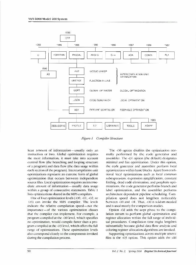
VAX 6000 Model 400 System
I
'ERCOMPILATION UNIT TlMlZATlON
C
ULD
UMERGE
UOPT
UGEN
AS1
GLOBAL OPTIMIZATION
UCODE LINKER I IF C
FUNCTION IN-LINE
GLOBAL OPTIMIZER
CODE GENERATOR
PIPELINE SCHEDULER PI
LOCAL OPTIMIZATION
FORTRAN
:PHOLE OPTIMIZATION
Figure I Cumpiler Stmctz~re
PASCAL
least amount of information-usually only an instruction or two. Global optimization requires the most information; it must take into account control flow (the branching and looping structure of a progmm) and data flow (the data usage within each section of the program). Intercompilation unit optimiucions represent an extreme form of global op timintion that occ~lrs between independent source files. Local optimization requires an interme- diate amount of information-usually data usage within a group of consecutive statements. Table 1 l~sts optimizations shared in the MIPS compilers.
One of four optimization levels (-00, - 0 1 , -02, or -03) can invoke the MIPS compiler. The levels indicate the relative compilation speed - not the importance - of the varkn~s optimization c h e s that the compiler can implement. For example, a program compiled at the -00 level, which specifics no optimization, would compile faster than a pco- gram compiled at thc -03 level, which offers the full range of optimintions. These optimization lcvels also correspond closely to the components invoked during the compilation process.
The -00 option disables the optimization nor- mally performed by the code generator and assembler. The -01 option (the default) designates nlinimal and fast optimization. Under this option, the code generator and assembler perform local optimizations within basic blocks. Apart from tradi- tional local optimizations such as local common subexprcssion, expression simplification, constant folding, dead code elimination, and peephole opti- mizations, the code generator performs branch and label optimization, and the assembler performs architecture-dependent pipeline scheduling. Com- pilation speed does not lengthen noticeably bctween -00 and -01. Thus, -00 is seldom needed and is used mostly for comparison studies.
Option -02 adds the uopt phase to the compi- lation stream to perform global optimization and register atltxation within the full range of individ- ual procedures. Compilation time might lengthen substantially because global data-flow analysis and coloring rgister-allocation algorithms are invoked.
Supporting optimizations across multiple source files is the -03 option. This option adds the uld
ANSI C
Vol. 2 No. 2, .Spring 1990 Digital TecbnicalJournal
C++. PL1 ADA COBOL

Compiler Optimization in KISC Systems
Table 1 Optimization Methods
Peephole optimization
Local optimization
Global optimization
lnstruction scheduling lnstruction selection lnstruction substitution Calllreturn selection Branch-to-branch optimization Local subexpression elimination Constant folding Expression simplification Dead code elimination Local register assignment Short-circuit evaluation Invariant code removal Strength reduction Global register assignment Global subexpression elimination Shrink-wrapping register saving Linear test replacement Loop unrolling Tail recursion Copy propagation Redundant store elimination
lntercompilation Interprocedural register allocation unit optimization In-line expansion of procedures
phase, which combines separate compilation units into a single file at the ~lcode level. Thus the option enables multimodule programs to achieve the same degree of optin~izatic.)n as single-module programs. The umerge phase selectively expands procedure calls by in-line substitution. The resulting ucode object is then sent into normal back-end optimi- zation and compilation stream starting with uopt. 'The -03 option causes uopt to perform interproce- dural register allocation; opt also benefits from the complete information in the linked ucode file to perform the other global optimizations normally associated with this phase.
Local Hardware Architecture MII'S' architectural design facilitates compiler opti- mization and overall system throughput. Important to system performance is the memory hierarchy. A split cache provides intlependent access to both instructions and data in a single cycle. A single com- bined cache would limit the processor to obtaining only a single instruction or data item each cycle.
The compiler design takes into consideration the effect of cache memory. On average, instruction references cache miss less frecluently than data ref- erences; this observation allows the compiler to prefer slightly longer instruction sequences if they avoid extra data references. The instruction cache miss rate is lower because the hardware loads multi-
ple contiguous words into the cache on a miss, and the sequential nature of instruction execution takes advantage of this locality.
Register optimization makes the most significant architecturelcompiler performance enhancement Because the optimizer knows that data allocated in registers can be accessed without delay, it places the most frequently used variables into registers. The optimizer computes the lifetime of individual data items and replaces the memory ucage with a register usage. The relatively large number of registers makes it likely that the optimizer can successfully promote the most frequently referenced variables into a register. (There are thirty two 32-bit integer registers and sixteen 64-bit floating-point registers )
One of the most important architectural features used to improve performance is the instruction pipeline. Although several cycles are required to actually complete the instruction, the processor can be viewed as if each instruction takes only one cycle because a new instruction is started each cycle. The compiler is aware of several exceptions; for exam- ple, load instructions require one instruction between the load and the use of the data loaded. This load-delay slot is used by the compiler for another instruction - effectively, the cache mem- ory access of the load executes in parallel with the other instruction. This technique 1s called instruc- tion scheduling. Other examples of parallel instruc- tion execution include
Overlapping a branch instruction with another operation
Testing for division by zero while the divide is in progress
Executing several different floating point oper- ations simultaneously (The MIPS processor has separate floating point add, multiply, and divide units.)
The MIPS architecture does not have condition codes. Although this seems unusual compared with many other machines, this design actually improves performance. 'The architecture provides branch instructions that both test a condition and then branch. Thus, the compiler must generate only one instruction for conditional branches rather than the two instructions usually required (one to test for the condition, then another to perform the branch). Only comparisons that compare larger (or smaller) values between two registers, or a register and immediate value, cannot be handled this way. The

VAX 6000 Model 400 System
compiler restructures most comparisons to avoid this case, thus decreasing average test time.
Instructions in a ClSC processor often have widely varying execution times. This difference makes it hard to determine which of several alterna- tive sequences is actually fastest. Because almost all RISC instructions take the same time, the optimizer can select the fastest sequence with relative ease.
Program Portability To make a system useful, programs must be ported onto the processor. The use of U M x operat- ing systems and standardized languages such as FORTRAN bas tremendously improved program portability. However, incorrect programs may have latent bugs that are masked by a naive compiler. Thus, an optimizing compiler tends to expose more of these problems. A naive FORTRAN compiler may assign all variables to memory locations, giving variables predictable initial values. An incorrect program that relies on these initial values will fail when an optimizing compiler assigns a variable to a fast register that tends to have unpredictable values.
An optimizer converts the program (as written) into one that is identical except that it executes faster. To do this, the optimizer must make assump- tions about what the programmer intended. Often the programmer depends on expericnce with previ- ous compiler implcmcntations rather than the rules of the 1:inguage.
The >,fIl'S compiler suite provides a number of options to allow :I program to run without modifi- cation in the presence of such common errors. This permits a program to be ported quickly, giving the programmer a choice as to when to correct the problem.
Traditionally, system vendors have added unique extensions to their language implementations. While these may be a boon to a programmer when writing the program, they can be a bane when it comes time to port the program. The MIPS com- pilers implement many industry-wide extensions to the standard language$ to make them compatible with other implementations. An important set of extensions is the support of Digital's VAX FORTFUN extensions. Another is the inclusion of IBM's PL1 extensions to pernlit an independent software vendor to port a 1.8-million-line PL1 program to the MlPS architecture.
Wherever estcnsions :Ire required, Mil's chooses proposed extensions for similar functions that arc being considered by the standarcis committecs. An example of this last situation is the need to repre-
sent hardware 110 structures when bcing rcfcr- enced by an optimizing compiler. Consider an 110 device register that is used to define the st:ctus of the 110 device. The optimizing compiler would see multiple references to the address without inter- vening assignments. The compiler would cleverly (but incorrectly) optimize all references to a proces- sor register. MIPS has added the key word volatile to indicate to the compiler that this variable changes in ways that the compiler cannot detect. This exten- sion was recently incorporated into the current ANSI standard for C , but i t was added to the MIPS C compiler four years ago.
Toob to Development Fundamental to system development is a tool set that aids in compiling, debugging, performance tun- ing, and system construction (bring-up). MIPS' tool set includes those tools traditionally found in UNIX operating systems, as well as tools unique to MIPS.
The multiple front-cnd, common back-end con- struction of the MlPS compilers provides a consis- tent set of languages to the developer. Options and flags are the same across all languages. In fact, cc can usually be used to compile programs in the other languages. All languages share a common linkage convention that makes it easy to write or port progr;tms written in two or more languages.
The ['NIX tool make provides a convenient method of program development. This tool iden- tifies which source modules of a program changed and rccompilcs only those modules. In recom- piling, tlrakc provides the correct compilation options. It also provides the complete set of cornpi- lation options; for example, the debugging option can be en;~bled through a nzuke target to trou- bleshoot a program. Later, the debugging options can be disabled, and higher levels of optimization can be spccificd in compiling the production version of the program. The make rules file, which accompanies the source program modules, deter- mines how the modules are t o be combined into the final run program. This prior determination elimi- nates the need for detailed written documentation or programmer support, making it simpler for developers to exchange source programs.
Crucial to eftjcient program development is a source-oricntecl debugger. MIPS provides an extended version of dbx which supports all pro- gramming languages. (ADA has a special debugger.) The debugger provides features such as print- ing variables = they change, or replaying a debug- ging session to a certain point before continuing
Val. 2 No. 2. .S/)ring 1990 Digilal TecbnicalJournal

Compiler Optimization in RlSC Systems
the debug session. The user can view and edit the source, as well as see each statement as it is executed.
The debugger also lets the user view the program in both the high-level language in which it was written and in the generated machine language. Thus, the user can set a breakpoint on a specified statement or instruction. Full debugging facilities are available only when the debugging option is specified. However, the compiler (by default) main- tains the line number tables in a compressed format in the load module even when the option is not specified. Retention of the line number tables per- mits partial debugging without the need to recom- pile the program using the debugging option. Line number information is kept for each instruction, permitting the instruction scheduler to move the instruction while keeping track of the line that originated it.
Specification of both debugging and optimization options can create conflicts. For example, it is possi- ble for a bug to appear only when a higher level of optimization is specified. Moreover, optimizations such as register allocation can confuse the debug- ger, because variables are not at the locations that it assumes. To avoid this situation, the MIPS compil- ers disable any optimization that interferes with debugging when both debugging and optimization options are specified. To debug the problem that shows up only in optimized code, a special option permits both the debugger and optimization to be enabled. This technique requires the developer to use caution when inquiring about the contents of a variable.
To tune a program for optimal performance, the developer must learn where in a program the time is spent and why. Traditional U N l X systems provide a method called pc sampling. With this technique, the system must interrupt a program at regular intervals (usually 60 or 100 times per second) and increment a per-location counter. After enough sample points are taken, a pattern of execution time emerges. This method has a severe flaw because modern processors execute 10 to 20 million instruc- tions per second; this means the number of samples is less than 1 in 100,000. The method requires a very long execution time to collect a statistically mean- ingful sample.
Although MIPS provides the pc sampling tech- nique, it also furnishes a more exacting method. Pixie is a tool that takes an executable load module and prepares it for measurement by inserting a counrer in every basic block. After running the
instrumented program, the counters are dumped to a file for analysis by several programs. Prof dis- plays tables of interesting information such as the following:
Number of CPU cycles for each source line
Number of times each function is called
Average number ofcycles in each call to a function
Figure 2 shows examples ofprof output listings. A second program, pljcstats, takes the same counts and displays information about the program in architectural terms, such as:
Number of cycles used for each instruction
Number of unused delay slots
Number of FLOPS
A general indication of cache locality
These two programs assume a perfect memory system, that is, no effect due to cache misses.
For a complete analysis, a cache simulator is also available that uses pMe to provide a memory address trace to the simulator to model the mem- ory system. MIPS uses this technique to plan new machine designs. Each proposed change to the system requires a detailed simulation to exhibit its effect. When a MIPS designer is convinced that a balanced and optimal point has been found, iniple- mentation begins. Experience with this technique has shown an accuracy of better than 4 percent when comparing predicted performance to actual performance.
An Optimization to Improve Cache Performance An area seldom addressed in compilers is the opti- mization of programs in memory to improve cache hit rates. Modern microprocessor performance has been increasing faster than the supporting memory systems. Taking advantage of this higher perfor- mance without introducing costly memories has required the use of small and high-speed cache memory. Cache memory contains recently used instructions and data. Hardware substitutes cache memory if the desired word is in the cache. This substitution is invisible (other than performance improvements) to the program. Each main memory location must share a cache location with other memory locations because the cache is smaller than main memory. For a cache to be effective, it must contain enough of the program or data to ensure multiple reuse of the instructions or data.
Dlgllcrl TecbnicnlJournal Vol. 2 No. 2, Spring 1990

VAX 6000 Model 400 System
cycles 8cycles sun lcall lllns
MI" IfI~f~nl.pl w~l~rn-cha~. t..IL.x~a~t~)t.~l urIte-~h*r I. . /L .~LoYCPUC.CI w r l L . - ~ h l l I../L.XLOYIPUt.cI rrlrn-lnr*grr I. .lr.xcourpur.cl 197
,"> v.uv avu.uv I5 9 wd I. ./L.XIOUIPUL.CI 90 0.00 100.00 81 0.00 100.00 35 0.00 100.00 u l n 1flxtonr.pl 35 0.00 100.00 rrln 1IIxIonL.pl 15 0.00 100.00 wrlt.-m~rlnq l../~=x~outpll.cl 150 44 511050 0.39 95.46 13 0.00 100.00
o,oo [open USED AN AVERAGE OF 82 ' vrltm-drars I. .lr.xrourpr .=I 48 4 561855 0.38 95.84
r 0.00 100.00 CYCLES PER CALL AND 13 BYTES rrI~.-ch.r= l..ll.xlo~tput.~l 41 4 567035 0.38 96.22 -rl~._chars I../L.XLOUL~JL.C) 49 28 487387 0.11 96.55
s 0.00 ~oo.oo PER LINE. I I I . 18 20 348150 0.24 96.79 5 0.00 100.00 c r e r t t../str np.rgl.*l main 1flxfonr.p) 31 100 318000 0.21 91.02 I
Figure 2 Emmples of prof Oulput Listings
A valuable optimization is to position the pro- gram in memory so that the most frecluently used memory locations never compete for the same cache locations. MIPS has built a tool called cord that rearranges the program to improve instruction cache utilization. This tool is made possible through the existence of precise profiling tools.
To use cord, the programmer compiles the pro- gram in the usual way. Pixie is used to add counters to the program for each basic block. After exe- cuting the instrumented program, prof is run with an option that creates a file containing dynamic execution information. That file is given to cord, along with the original executable module.
Cord computes the density for each function (procedure). The density is defined as the average number of cycles executed by each instruction in the function. Figure 3 is an example of eight functions, their sizes, cycle counts, and density. Cord then creates a new executable module after sorting the functions according to density. Figure 3 also shows the order of the functions in the rear- ranged program.
This sort improves cache hit rate because it places the functions that use the most cycles in memory so they do not compete for the same cache location as other frequently executing functions. The effectiveness of sort is helped by two other features in the MIPS architecture. First, the caches are direct-mapped to memory so that each memory location corresponds to a single cache location. Sec-
ond, the MIPS operating system places virtual pages in physical memory so that adjacent virtual pages map to adjacent cache pages. As a result, the place- ment of functions by cord has very predictable effects on the cache.
Figure 3 also shows the arrangement in an unexpected way. Rather than placing the densest function (A) at the beginning of memory, it is placed farthest from the start of the cache. This arrange-
MEMORY ADDRESSES
KEY.
NAME A B C D E F G H
SIZE 12K 24K 20K 8K
16K 12K 16K 20K
CYCLES 960K
1680K 1200K 400K 640K 360K 320K 200K
DENSITY 80 70 60 50 40 30 20 10
Figure 3 Cache Performance improved by cord
Val. 2 No. 2, Sp'ng 1990 Digflal TecbnicalJounual

ment has the effect of making the densest func- tion share cache locations with the function 128 kilobytes (twice the cache size) away (H). Cord improves performance by as much as 20 percent to 30 percent on programs exceeding the size cache. It works solely by improving the efficiency of the instruction cache. Methods to improve data cache accesses are not available yet because of the more random nature of data accesses and difficulty in get- ting accurate data reference information.
An advanced architectural simulator, Sable mod- els (in C) the processor, including TLB, pipeline, register set, and system design, incorporating the cache subsystem, main memory, and 110 interface. Developers can customize Sable for a unique system design. Sable has been used routinely at MIPS to bring up the UNrX operating system before hard- ware is available. Simulation with Sable assures that the software is reliable and performs optimally when the hardware is actually available. Sable can be osed with the debugger to provide full symbolic debugging in the simulation environment. Also, Sable can provide the same address traces thatpixie provides to analyze operating system performance. After a system has been brought up using Sable, other tools can assist in constructing the system on the real hardware. A simple debug monitor is available to work with the symbolic debugger to provide a symbolic debugging environment on the real hardware.
Compiler Optimization in RISC S p t m
Compilers are taking better advantage of the paral- lelism in today's RISC processors. Evidence of this can be seen in the scheduling of instructions to capitalize on load and branch delays and multiple floating point units. This trend will continue as it becomes feasible to build effective multiprocessor systems. In this area, compilers that will partition a problem across multiple processors - each per- forming a portion of the iterations of a loop- will be seen. A major challenge will be to find ways to use this kind of parallelism in nonengineering prob- lems. These problems tend not to be loop intensive and will require a breakthrough in compiler tech- nology for automatic parallelism.
Over the past five to ten years, the programming language c has come to the forefront as a major systems language. While C offers many advantages, it requires a user to deal with fairly primitive struc- tures rather than abstractions. C++ will offer much of the flexibility of C with the added capability of data abstraction.
It is expected that future compilers will take advantage of optimizations that reduce cache misses. These optimizations include loop inter- change, which reorders the accesses to an array to improve locality of data references, and software pipelining, which takes better advantage of over- lapping memory accesses and computation.
Digital TechnicalJournal Vo1. 2 No. 2, Spring 1990 95

The Digital Technic:tl Journal pub1ishesp~rf)er.s that c>.vpk)re the tecr"nzologiccrlfi)zrthtiom of Digital's rn~ljorproducts. Each JozrrnalJbc~es on at leust one prodzrcl circa andprescwts a cotnf~il~ztiotr oJj)uf~c~rs iuritten by the et7gitiecn u~bo de~r~elo~~ed the product. Thr cotztc~tztfii' the Journal is st~leclcvi b j ~ fhc> Jorrrnrrl Adz~isor:~) Board.
li)pics covered in previous issues o f the nigir(i1 7hcL~rzical Jourrzrd are as follows:
VAX 8600 Processor Vol. 1, No. I , Azrgzat 1985
MicroVAX I1 System W)l. I, No. 2, hlarcb 1086
Networking Products K)l, I . ,Vo. 3, Septen~ber I%%
VAX 8800 Family Vol. I, No. 4, Februa?:~ I9S7
VAXcluster Systems Vol. I, No. 5, September 198'
Software Productivity Tools vol. I, No. 6, Februaly 1988
CVAX-based Systems W)l. I , No. 7, Au~qmt 1988
Storage Technology Vol. I, No. 8, Februaq, 1989
Distributed Systems Vol. I, No. 9, June 19W)
Compound Document Architecture %l. 2, No. I , Winter 1990
See the inside front cover of this issue for subscrip- tion information.
Single copies and past issues o f the Digital Technical J(~urnu1 can be ordered from Digital Press at a cost of $16.00 per copy.
Digital Press is Digital Equipment Corpor;ttion's international publkkr of books for computcr pro- fessionals. Copies of the new titles now available from Digital Press that are listed below can bc ordercd by writing to Digital Yrcss, Departmcnt DTJ, 12 Crosby Drive, Bedford, MA 01730, U.S.A.
COMMON LISP: The Language Guy Steele Jr., Second lidition. 1990 (S38.95 in softcovcr. S44.95 in clothcover)
The Matrix: Computer Networks and Confereadng Systems Worldwide John Quarterman, 1990 (S49.95)
UNIX for VMS Users I'hilip Bourne, 1990 (528.95)
The W User's Guide James Peccrs and Patrick Holmay, 1990 ($23.00)
A Beginner's Guide to VAX VMS Utilities and Applications Ronald Sawey and Troy Stokes, 1989 (523.00)
VMS Internals and Data Structures: Version 5 Update Xpress Ruth Goldenberg and Lawrence Kenah, Volumes 1, 2, and 3, 1989($35.00)
VAXNMS Internals and Data Structures: Version 4.4 Lawrence Kenah, Ruth Goldenberg, and Simon Bate, I988 (875.00)
Digital Guide to Software Development Corporate User Publications Group of Digital Equipment Corpordtion, 1990 ($27.95)
Technical Aspects of Data Communication John McNamara, Third Edition, 1988 ($42.00)
Information Technology Standardization: Theory, Practice, and Organizations Carl Cargill, 1989 (924.95)
Computer Programming and Architecture: The VAX Henry 1-evy and Richard Eckhouse, Second Edition, 1989 (824.95)
ABCs of MUMPS: An Introduction for Novice and Intermediate Programmers Richard Walters, 1989 (824.95)
Nl. 2 No 2. . \ ; / ) r i t ~ 1990 Digilul TecbnicalJortmrrl

ISSN 0898-90 1X
Primed in USA. EYC197&DP190 04 02 30.0 BUO Copyright 1990 DI&id -1 W t i O n RighB Reserved