Embed Size (px)
Citation preview
Digital Techniques III
Project Specification 2015
University of Oulu Electronics Laboratory
Table of Contents
Table of Contents Revision History 1. Introduction
1.1. audioport IP Block Overview 1.2. Project Overview
2. audioport Architecture Description 2.1. control_unit 2.2. dsp_unit 2.3. cdc_unit 2.4. i2s_unit 2.5. Highlevel operating principle
3. Functional Requirements 3.1. Design Parameters 3.2. Interface Description
3.2.1. Clocks and resets 3.2.2. Inputs and Outputs
3.3. Memory Map of Registers 3.3.1. Command Register (CMD_REG) 3.3.2. Level Register (LEVEL_REG) 3.3.3. Configuration Register (CFG_REG) 3.3.4. Filter Coefficient Data Registers 3.3.5. FIFO Registers
3.4. Block Specifications of Functional Units 4. Design Environment
4.1. Linux Environment Settings 4.2. The project directory 4.3. 0_setup_design.tcl file
5. Project Tasks and Schedule 6. Task 1: Design Initialization
6.1. audioport Control Register Memory Map Design 6.2. Design Parameters Setup 6.3. SystemVerilog Design Hierarchy Creation 6.4. Documentation 6.5. Tasks 2 10.
References
Revision History
Version Date Author Comment
1.0 3.2.2015 J.L. Initial version
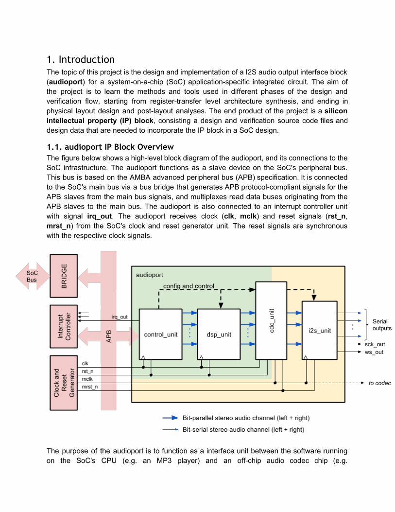
1. Introduction The topic of this project is the design and implementation of a I2S audio output interface block (audioport) for a systemonachip (SoC) applicationspecific integrated circuit. The aim of the project is to learn the methods and tools used in different phases of the design and verification flow, starting from registertransfer level architecture synthesis, and ending in physical layout design and postlayout analyses. The end product of the project is a silicon intellectual property (IP) block, consisting a design and verification source code files and design data that are needed to incorporate the IP block in a SoC design.
1.1. audioport IP Block Overview The figure below shows a highlevel block diagram of the audioport, and its connections to the SoC infrastructure. The audioport functions as a slave device on the SoC's peripheral bus. This bus is based on the AMBA advanced peripheral bus (APB) specification. It is connected to the SoC's main bus via a bus bridge that generates APB protocolcompliant signals for the APB slaves from the main bus signals, and multiplexes read data buses originating from the APB slaves to the main bus. The audioport is also connected to an interrupt controller unit with signal irq_out. The audioport receives clock (clk, mclk) and reset signals (rst_n, mrst_n) from the SoC's clock and reset generator unit. The reset signals are synchronous with the respective clock signals.
The purpose of the audioport is to function as a interface unit between the software running on the SoC's CPU (e.g. an MP3 player) and an offchip audio codec chip (e.g.
digitaltoanalog converter). The audioport appears as a memorymapped slave device to the CPU. When the CPU writes audio data to FIFO buffers inside the audioport's control_unit block, the audioport converts them to serial audio streams that comply with the I2S protocol that is supported by most audio codec chips. The CPU can also perform various control tasks on the audioport by writing to memorymapped control registers inside the control_unit. When the audioport has consumed all audio data from its FIFO buffers it can request new data from the CPU by raising the interrupt signal. The audioport contains a digital signal processing unit (dsp_unit) that can be used to perform various signal processing tasks on the audio data before it is send out through the I2S interface unit (i2s_unit). The audio_port consists of two mutually asynchronous clock domains. The control_unit and dsp_unit use the clock signal clk that is common to the APB subsystem. The i2s_unit uses a clock signal mclk that also functions as a system clock for the external audio codec chip. The two clock domains, indicated with green and yellow colors in the figure above, are connected to each other with a clock domain crossing unit (cdc_unit) that implements the required handshaking and synchronization functions.
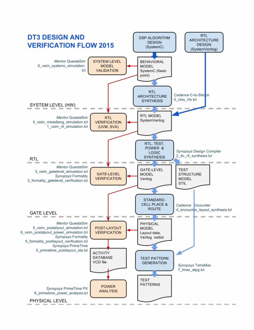
1.2. Project Overview The aims of the project is to create a synthesizable register transfer level (RTL) model of the audioport, and then implement it using logic synthesis and integrated circuit layout generation tools. The RTL model will be created partly "manually" by the designer, and partly automatically from algorithmlevel models using a highlevel synthesis tool. The algorithmlevel models are created and validated using SystemC. The RTL models are implemented in SystemVerilog, and verified using an Universal Verification Method (UVM) compliant simulation testbench and SystemVerilog assertions. Assertions are also checked using a formal verification tool. In the logic synthesis phase, designfortestability and powersaving structures are added to the circuit. After the IC layout has been created, the designs area, timing and power consumption estimates are created using postlayout simulation and static timing analysis tools. Finally, test patterns for manufacturing tests are created. The complete design flow and the tools used is shown in the next figure. The project consists of three main phases:
1. In the first phase, the "traditional" digital ASIC design and verification process is learned by designing the control_unit from RTL to layout.
2. In the next phase, the RTL models for parts of the dsp_unit are created using SystemC and highlevel synthesis
3. In the final part, the remaining RTL parts are created, and the complete design is integrated and implemented using the RTLtolayout design flow learned in the first phase.
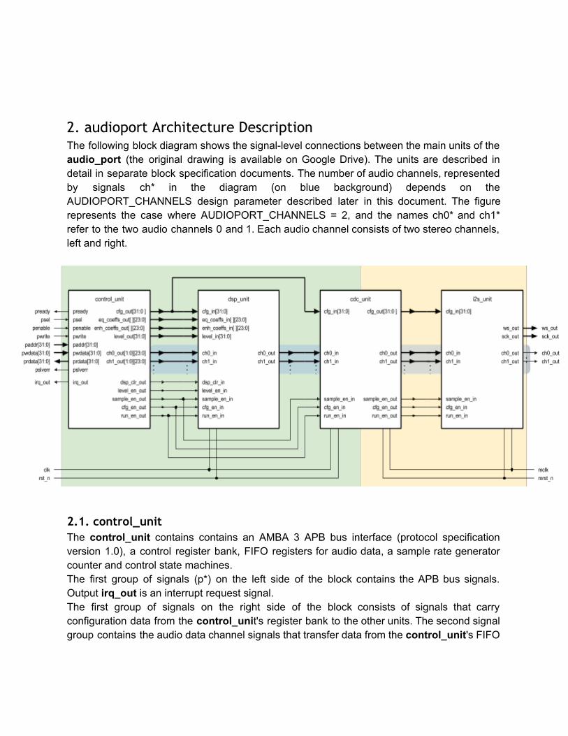
2. audioport Architecture Description The following block diagram shows the signallevel connections between the main units of the audio_port (the original drawing is available on Google Drive). The units are described in detail in separate block specification documents. The number of audio channels, represented by signals ch* in the diagram (on blue background) depends on the AUDIOPORT_CHANNELS design parameter described later in this document. The figure represents the case where AUDIOPORT_CHANNELS = 2, and the names ch0* and ch1* refer to the two audio channels 0 and 1. Each audio channel consists of two stereo channels, left and right.
2.1. control_unit The control_unit contains contains an AMBA 3 APB bus interface (protocol specification version 1.0), a control register bank, FIFO registers for audio data, a sample rate generator counter and control state machines. The first group of signals (p*) on the left side of the block contains the APB bus signals. Output irq_out is an interrupt request signal. The first group of signals on the right side of the block consists of signals that carry configuration data from the control_unit's register bank to the other units. The second signal group contains the audio data channel signals that transfer data from thecontrol_unit's FIFO
registers to the dsp_unit. The third signal group contains control and timing signals that are driven by a statemachine and the sample rate counter in the control_unit. The control_unit serves three kinds of purposes:
● storage of configuration data in a control data register bank, ● storage of audio data in FIFO register banks, and ● processing of commands that the host CPU sends to the audioport by writing
command codes to specific registers in the control data register bank.
2.2. dsp_unit The dsp_unit contains digital signal processing blocks that can be used to process the audio data before it it sent to the i2s_unit. The DSP blocks are:
● eq_filter (equalization filter) ● enh_filter (stereo enhancement filter) ● scaler (output level scaler)
All audio channels are processed by the scaler, but the eq_filter and enh_filter can be enabled individually on each channel. In addition to the DSP blocks, the dsp_unit contains control logic that that is used to enable and/or bypass each DSP block on each channel, and registers for storing data produced by one block and waiting to be consumed by the next block in the signal chain.
2.3. cdc_unit The clock domain crossing block cdc_unit contains synchronizer flipflops and handshaking statemachines that are needed to transfer data from the clk clock domain to the mclk clock domain.
2.4. i2s_unit The i2s_unit contains "serializer" shiftregisters that transform parallel audio data into serial bitstreams that conform to the I2S protocol specification. Thei2c_unitalso generates the I2S serial bitclock (sck) and wordselect (ws) signals.
2.5. High-level operating principle A typical operating sequence for the audioport consists of the following steps:
1. Configuration phase, where the host CPU configures the dsp_unit, sets the sample rate and output level by writing data to control registers in the control_unit. The CPU can also fill the audio data FIFO register banks in this phase.
2. Device start, which happens when the host CPU writes a 'run' command into a control register. The control_unit sets the run_en signal high in response to this command to notify the other units, and enables the sample rate counter.
3. During the run phase, the audioport reads and processes audio data samples from the FIFO register banks. When all data from the FIFO register banks have been consumed, the control_unit requests the host CPU to fill the FIFO buffers by activating the interrupt request signal irq_out. During the run phase, the host CPU can

also control some functions of the audioport. It can change the output level scaling, for instance.
4. Stopped phase, which begins when the host CPU sends a 'stop' command to the control_unit. Audio data processing stops but the audioport retains its configuration.
During the run phase, the data processing rate is set by the sample_en signal that the control unit generates using a counter. This signal is set to state 1 for one clock cycle in the beginning of the processing cycle. The sample_en signal serves the following purposes:
● It notifies the dsp_unit that the next audio data samples are available in the control_unit's audio output ports (ch*_out). The dsp_unit must read this data on the rising edge of clk when sample_en == '1.
● It notifies the cdc_unit that the results of the processing of the previous audio sample are available at the outputs of the dsp_unit. The cdc_unit must read this data on the rising edge of clk when sample_en == '1. The cdc_unit synchronizes the sample_en and audio data signals (and other signals) to the mclk clock signal used by the i2s_unit.
● The i2s_unit reads next audio data samples from the cdc_unit to its internal register. ● Next data samples are read from the audio data FIFO register banks and placed in the
ch*_out outputs of the control_unit. The audioport supports sample rates 48kHz, 96kHz and 192kHz. The host CPU selects the sample rate by writing configuration data to a register. The sample_en cycle sets some fixed timing constraints for the audioport and the system:
● The dsp_unit and the cdc_uniti2s_unit combination must process an audio data sample in one sample_en pulse interval (at max. rate 192 kHz)
● The CPU must fill the FIFO buffers before the next sample_en pulse after the irq_out signal is activated. The CPU's interrupt latency must therefore be less than 1/192kHz.
The following constraints are set to the software running on the host CPU:
● The CPU must fill all audio data FIFO buffers at the same time and to the same level. The control_unit only tracks the level of the FIFO register banks of the first channel and generates interrupt requests on the basis of that information.
● The sample rate cannot be changed when the audioport is in the 'run' mode.
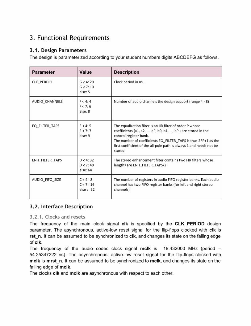
3. Functional Requirements
3.1. Design Parameters The design is parameterized according to your student numbers digits ABCDEFG as follows.
Parameter Value Description
CLK_PERDIO G < 4: 20 G < 7: 10 else: 5
Clock period in ns.
AUDIO_CHANNELS F < 4: 4 F < 7: 6 else: 8
Number of audio channels the design support (range 4 - 8)
EQ_FILTER_TAPS E < 4: 5 E < 7: 7 else: 9
The equalization filter is an IIR filter of order P whose coefficients {a1, a2, ..., aP, b0, b1, ..., bP } are stored in the control register bank. The number of coefficients EQ_FILTER_TAPS is thus 2*P+1 as the first coefficient of the all-pole path is always 1 and needs not be stored.
ENH_FILTER_TAPS D < 4: 32 D < 7: 48 else: 64
The stereo enhancement filter contains two FIR filters whose lengths are ENH_FILTER_TAPS/2
AUDIO_FIFO_SIZE C < 4: 8 C < 7: 16 else : 32
The number of registers in audio FIFO register banks. Each audio channel has two FIFO register banks (for left and right stereo channels).
3.2. Interface Description
3.2.1. Clocks and resets The frequency of the main clock signal clk is specified by the CLK_PERIOD design parameter. The asynchronous, activelow reset signal for the flipflops clocked with clk is rst_n. It can be assumed to be synchronized toclk, and changes its state on the falling edge of clk. The frequency of the audio codec clock signal mclk is 18.432000 MHz (period = 54.25347222 ns). The asynchronous, activelow reset signal for the flipflops clocked with mclk is mrst_n. It can be assumed to be synchronized tomclk, and changes its state on the falling edge of mclk. The clocks clk and mclk are asynchronous with respect to each other.
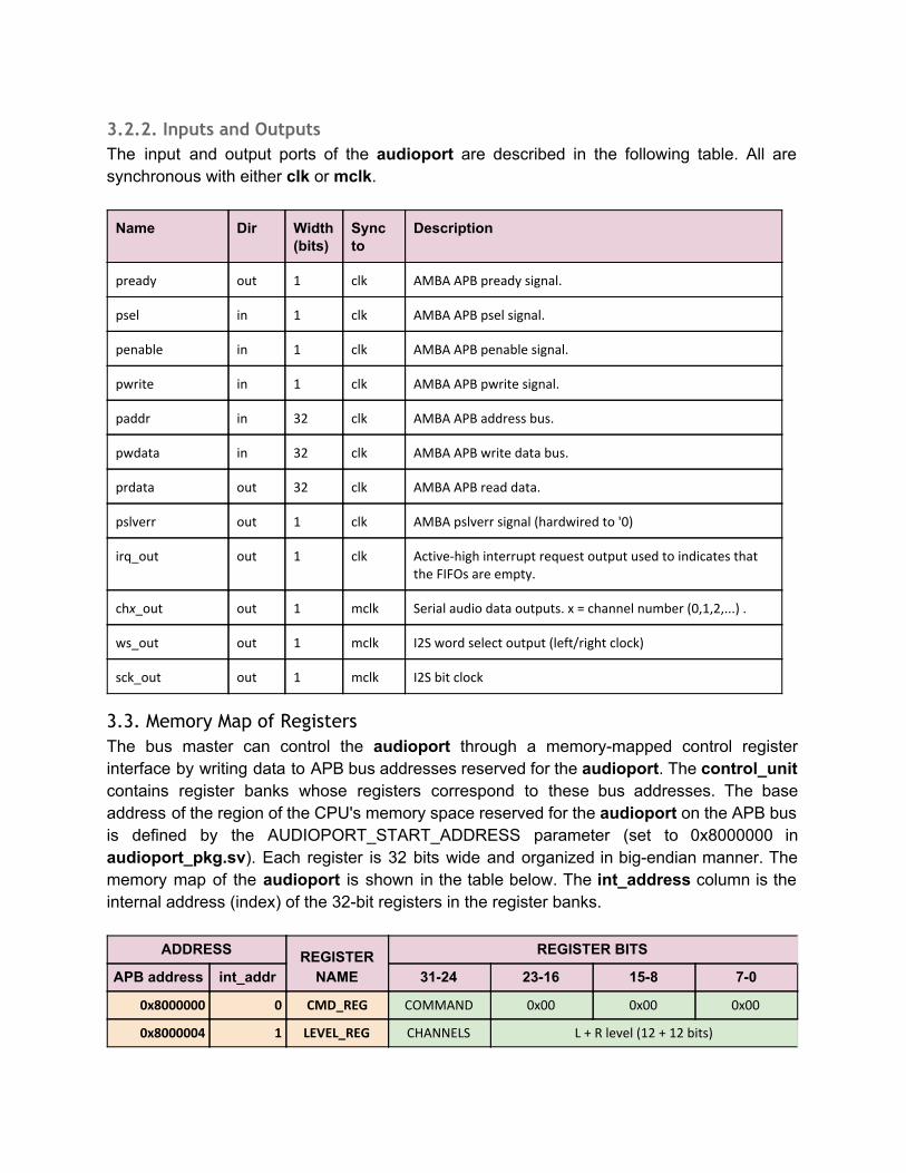
3.2.2. Inputs and Outputs The input and output ports of the audioport are described in the following table. All are synchronous with either clk or mclk.
Name Dir Width (bits)
Sync to
Description
pready out 1 clk AMBA APB pready signal.
psel in 1 clk AMBA APB psel signal.
penable in 1 clk AMBA APB penable signal.
pwrite in 1 clk AMBA APB pwrite signal.
paddr in 32 clk AMBA APB address bus.
pwdata in 32 clk AMBA APB write data bus.
prdata out 32 clk AMBA APB read data.
pslverr out 1 clk AMBA pslverr signal (hardwired to '0)
irq_out out 1 clk Active-high interrupt request output used to indicates that the FIFOs are empty.
chx_out out 1 mclk Serial audio data outputs. x = channel number (0,1,2,...) .
ws_out out 1 mclk I2S word select output (left/right clock)
sck_out out 1 mclk I2S bit clock
3.3. Memory Map of Registers The bus master can control the audioport through a memorymapped control register interface by writing data to APB bus addresses reserved for theaudioport. Thecontrol_unit contains register banks whose registers correspond to these bus addresses. The base address of the region of the CPU's memory space reserved for theaudioporton the APB bus is defined by the AUDIOPORT_START_ADDRESS parameter (set to 0x8000000 in audioport_pkg.sv). Each register is 32 bits wide and organized in bigendian manner. The memory map of the audioport is shown in the table below. The int_address column is the internal address (index) of the 32bit registers in the register banks.
ADDRESS REGISTER NAME
REGISTER BITS
APB address int_addr 3124 2316 158 70
0x8000000 0 CMD_REG COMMAND 0x00 0x00 0x00
0x8000004 1 LEVEL_REG CHANNELS L + R level (12 + 12 bits)
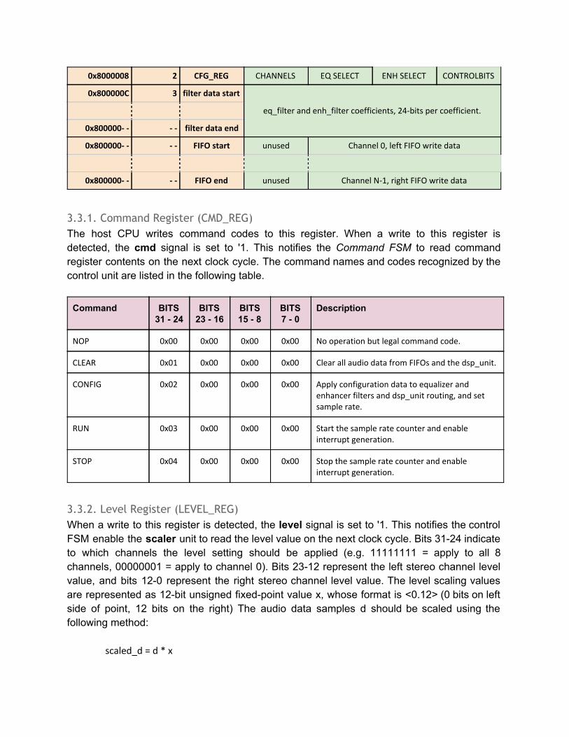
0x8000008 2 CFG_REG CHANNELS EQ SELECT ENH SELECT CONTROLBITS
0x800000C 3 filter data start
eq_filter and enh_filter coefficients, 24-bits per coefficient.
0x800000- - - - filter data end
0x800000- - - - FIFO start unused Channel 0, left FIFO write data
0x800000- - - - FIFO end unused Channel N-1, right FIFO write data
3.3.1. Command Register (CMD_REG) The host CPU writes command codes to this register. When a write to this register is detected, the cmd signal is set to '1. This notifies the Command FSM to read command register contents on the next clock cycle. The command names and codes recognized by the control unit are listed in the following table.
Command BITS 31 24
BITS 23 16
BITS 15 8
BITS 7 0
Description
NOP 0x00 0x00 0x00 0x00 No operation but legal command code.
CLEAR 0x01 0x00 0x00 0x00 Clear all audio data from FIFOs and the dsp_unit.
CONFIG 0x02 0x00 0x00 0x00 Apply configuration data to equalizer and enhancer filters and dsp_unit routing, and set sample rate.
RUN 0x03 0x00 0x00 0x00 Start the sample rate counter and enable interrupt generation.
STOP 0x04 0x00 0x00 0x00 Stop the sample rate counter and enable interrupt generation.
3.3.2. Level Register (LEVEL_REG) When a write to this register is detected, the level signal is set to '1. This notifies the control FSM enable the scaler unit to read the level value on the next clock cycle. Bits 3124 indicate to which channels the level setting should be applied (e.g. 11111111 = apply to all 8 channels, 00000001 = apply to channel 0). Bits 2312 represent the left stereo channel level value, and bits 120 represent the right stereo channel level value. The level scaling values are represented as 12bit unsigned fixedpoint value x, whose format is <0.12> (0 bits on left side of point, 12 bits on the right) The audio data samples d should be scaled using the following method:
scaled_d = d * x
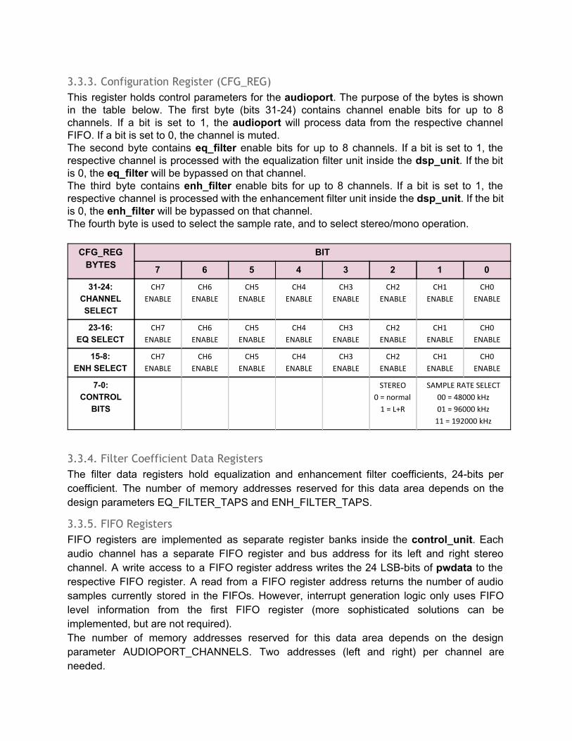
3.3.3. Configuration Register (CFG_REG) This register holds control parameters for the audioport. The purpose of the bytes is shown in the table below. The first byte (bits 3124) contains channel enable bits for up to 8 channels. If a bit is set to 1, the audioport will process data from the respective channel FIFO. If a bit is set to 0, the channel is muted. The second byte contains eq_filter enable bits for up to 8 channels. If a bit is set to 1, the respective channel is processed with the equalization filter unit inside the dsp_unit. If the bit is 0, the eq_filter will be bypassed on that channel. The third byte contains enh_filter enable bits for up to 8 channels. If a bit is set to 1, the respective channel is processed with the enhancement filter unit inside thedsp_unit. If the bit is 0, the enh_filter will be bypassed on that channel. The fourth byte is used to select the sample rate, and to select stereo/mono operation.
CFG_REG BYTES
BIT
7 6 5 4 3 2 1 0
3124: CHANNEL SELECT
CH7
ENABLE
CH6
ENABLE
CH5
ENABLE
CH4
ENABLE
CH3
ENABLE
CH2
ENABLE
CH1
ENABLE
CH0
ENABLE
2316: EQ SELECT
CH7
ENABLE
CH6
ENABLE
CH5
ENABLE
CH4
ENABLE
CH3
ENABLE
CH2
ENABLE
CH1
ENABLE
CH0
ENABLE
158: ENH SELECT
CH7
ENABLE
CH6
ENABLE
CH5
ENABLE
CH4
ENABLE
CH3
ENABLE
CH2
ENABLE
CH1
ENABLE
CH0
ENABLE
70: CONTROL
BITS
STEREO
0 = normal
1 = L+R
SAMPLE RATE SELECT
00 = 48000 kHz
01 = 96000 kHz
11 = 192000 kHz
3.3.4. Filter Coefficient Data Registers The filter data registers hold equalization and enhancement filter coefficients, 24bits per coefficient. The number of memory addresses reserved for this data area depends on the design parameters EQ_FILTER_TAPS and ENH_FILTER_TAPS.
3.3.5. FIFO Registers FIFO registers are implemented as separate register banks inside the control_unit. Each audio channel has a separate FIFO register and bus address for its left and right stereo channel. A write access to a FIFO register address writes the 24 LSBbits of pwdata to the respective FIFO register. A read from a FIFO register address returns the number of audio samples currently stored in the FIFOs. However, interrupt generation logic only uses FIFO level information from the first FIFO register (more sophisticated solutions can be implemented, but are not required). The number of memory addresses reserved for this data area depends on the design parameter AUDIOPORT_CHANNELS. Two addresses (left and right) per channel are needed.
3.4. Block Specifications of Functional Units The detailed functional requirements and design guides for the control_unit, dsp_unit, cdc_unit, and the i2s_unit are given in separate documents.
4. Design Environment The design work is done using Linuxbased electronics design automation (EDA) tools from Mentor Graphics, Synopsys, and Cadence Design Systems. The tools are available to student through the EUROPRACTICE program funded by the European Union. The IC technology used in the project is NANGate's 45 nm Open Cell CMOS standard cell library.
4.1. Linux Environment Settings Linux settings for the design programs must be sourced from file /research/ellab/public/Opetus/DT3_2015/dt3_settings.txt into the Linux command shell. To make this easier, the following alias command can be added at the end of the .cshrc file located in the home directory. It is a hidden dotfile, but can be edited as a normal text file (e.g. gedit .cshrc).
alias dt3 'source /research/ellab/public/Opetus/DT3_2015/dt3_settings.txt'
Every time before you begin to work, execute the command dt3 to read the settings.
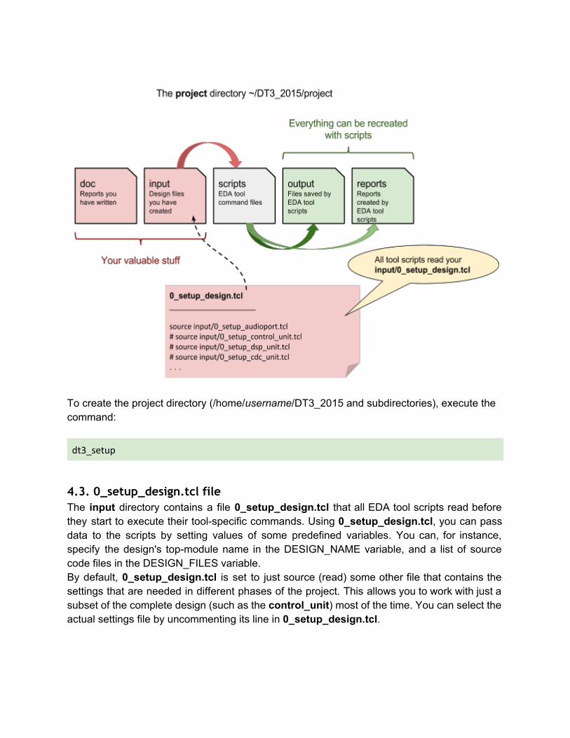
4.2. The project directory All your project data will be stored in the directory /home/username/DT3_2015/project. This directory contains five subdirectories, whose purpose is as follows:
Subdirectory Purpose
doc Documents you have written.
input All design data you have created.
scripts EDA tool command script files that are used to carry out specific design tasks, such as simulation. If you want to modify any script, first create a copy of the file, and modify the copy. This allows the original scripts to be updated automatically.
output Design data saved by the EDA tools. All data in this directory can be recreated using the scripts, so if your database becomes garbled, you can empty this directory and start over. Some scripts will delete or overwrite data in this directory, so don't keep anything valuable here.
reports Reports created by the EDA tools automatically. Files in this directory can be recreated using the scripts. Some scripts will delete or overwrite data in this directory, so don't keep anything valuable here.
To create the project directory (/home/username/DT3_2015 and subdirectories), execute the command:
dt3_setup
4.3. 0_setup_design.tcl file The input directory contains a file 0_setup_design.tcl that all EDA tool scripts read before they start to execute their toolspecific commands. Using 0_setup_design.tcl, you can pass data to the scripts by setting values of some predefined variables. You can, for instance, specify the design's topmodule name in the DESIGN_NAME variable, and a list of source code files in the DESIGN_FILES variable. By default, 0_setup_design.tcl is set to just source (read) some other file that contains the settings that are needed in different phases of the project. This allows you to work with just a subset of the complete design (such as thecontrol_unit) most of the time. You can select the actual settings file by uncommenting its line in 0_setup_design.tcl.

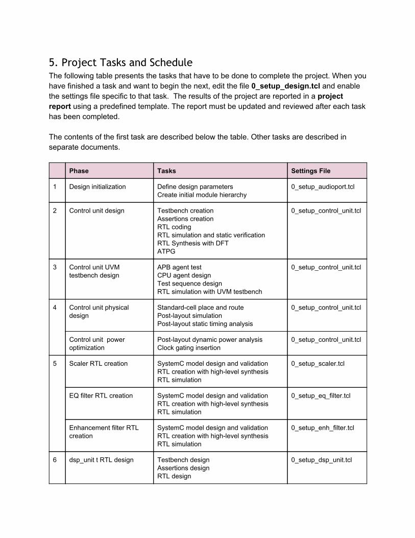
5. Project Tasks and Schedule The following table presents the tasks that have to be done to complete the project. When you have finished a task and want to begin the next, edit the file 0_setup_design.tcl and enable the settings file specific to that task. The results of the project are reported in a project report using a predefined template. The report must be updated and reviewed after each task has been completed. The contents of the first task are described below the table. Other tasks are described in separate documents.
Phase Tasks Settings File
1 Design initialization Define design parameters Create initial module hierarchy
0_setup_audioport.tcl
2 Control unit design Testbench creation Assertions creation RTL coding RTL simulation and static verification RTL Synthesis with DFT ATPG
0_setup_control_unit.tcl
3 Control unit UVM testbench design
APB agent test CPU agent design Test sequence design RTL simulation with UVM testbench
0_setup_control_unit.tcl
4 Control unit physical design
Standardcell place and route Postlayout simulation Postlayout static timing analysis
0_setup_control_unit.tcl
Control unit power optimization
Postlayout dynamic power analysis Clock gating insertion
0_setup_control_unit.tcl
5 Scaler RTL creation SystemC model design and validation RTL creation with highlevel synthesis RTL simulation
0_setup_scaler.tcl
EQ filter RTL creation SystemC model design and validation RTL creation with highlevel synthesis RTL simulation
0_setup_eq_filter.tcl
Enhancement filter RTL creation
SystemC model design and validation RTL creation with highlevel synthesis RTL simulation
0_setup_enh_filter.tcl
6 dsp_unit t RTL design Testbench design Assertions design RTL design
0_setup_dsp_unit.tcl
RTL code creation RTL simulation and static verification
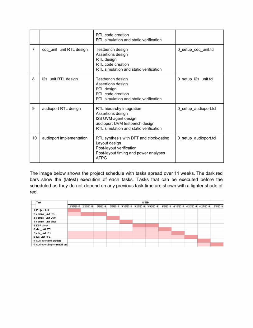
7 cdc_unit unit RTL design Testbench design Assertions design RTL design RTL code creation RTL simulation and static verification
0_setup_cdc_unit.tcl
8 i2s_unit RTL design Testbench design Assertions design RTL design RTL code creation RTL simulation and static verification
0_setup_i2s_unit.tcl
9 audioport RTL design RTL hierarchy integration Assertions design I2S UVM agent design audioport UVM testbench design RTL simulation and static verification
0_setup_audioport.tcl
10 audioport implementation RTL synthesis with DFT and clockgating Layout design Postlayout verification Postlayout timing and power analyses ATPG
0_setup_audioport.tcl
The image below shows the project schedule with tasks spread over 11 weeks. The dark red bars show the (latest) execution of each tasks. Tasks that can be executed before the scheduled as they do not depend on any previous task time are shown with a lighter shade of red.
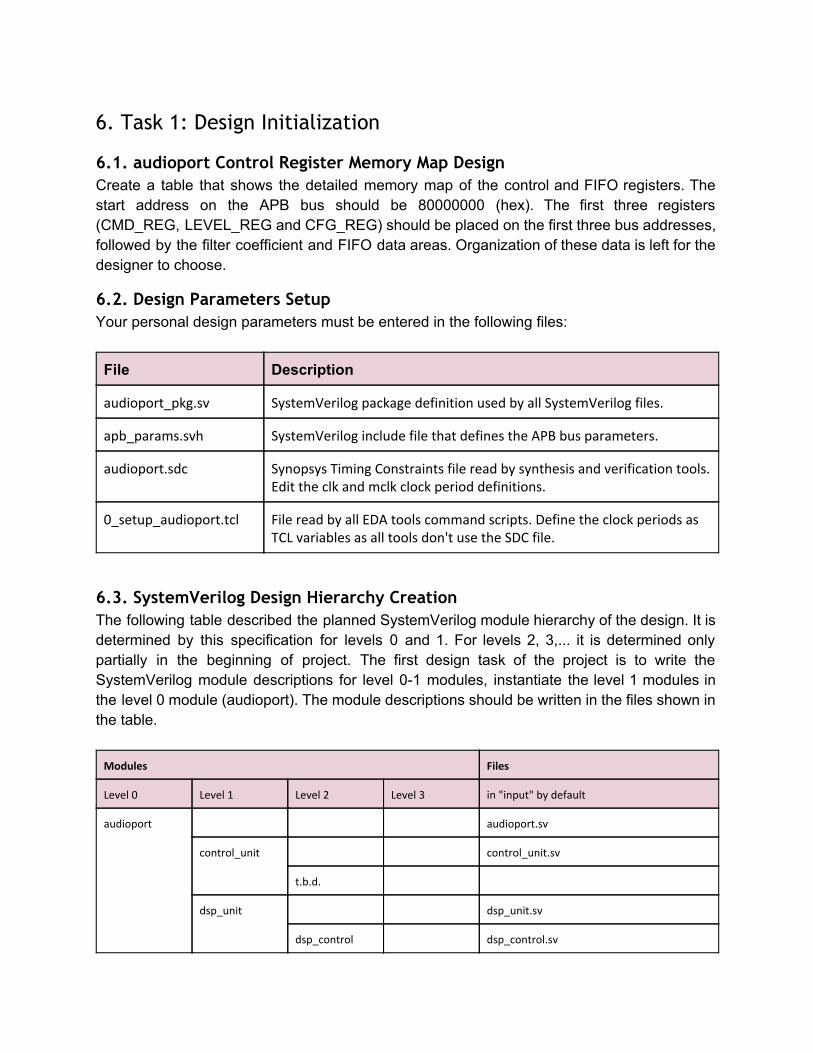
6. Task 1: Design Initialization
6.1. audioport Control Register Memory Map Design Create a table that shows the detailed memory map of the control and FIFO registers. The start address on the APB bus should be 80000000 (hex). The first three registers (CMD_REG, LEVEL_REG and CFG_REG) should be placed on the first three bus addresses, followed by the filter coefficient and FIFO data areas. Organization of these data is left for the designer to choose.
6.2. Design Parameters Setup Your personal design parameters must be entered in the following files:
File Description
audioport_pkg.sv SystemVerilog package definition used by all SystemVerilog files.
apb_params.svh SystemVerilog include file that defines the APB bus parameters.
audioport.sdc Synopsys Timing Constraints file read by synthesis and verification tools. Edit the clk and mclk clock period definitions.
0_setup_audioport.tcl File read by all EDA tools command scripts. Define the clock periods as TCL variables as all tools don't use the SDC file.
6.3. SystemVerilog Design Hierarchy Creation The following table described the planned SystemVerilog module hierarchy of the design. It is determined by this specification for levels 0 and 1. For levels 2, 3,... it is determined only partially in the beginning of project. The first design task of the project is to write the SystemVerilog module descriptions for level 01 modules, instantiate the level 1 modules in the level 0 module (audioport). The module descriptions should be written in the files shown in the table.
Modules Files
Level 0 Level 1 Level 2 Level 3 in "input" by default
audioport audioport.sv
control_unit control_unit.sv
t.b.d.
dsp_unit dsp_unit.sv
dsp_control dsp_control.sv

t.b.d
eq_filter eq_filter.sv
eq_filter_rtl output/eq_filter_hls_rtl.v (synthesized from eq_filter.cpp)
enh_filter enh_filter.sv
enh_filter_rtl output/enh_filter_hls_rtl.v (synthesized from enh_filter.cpp)
scaler scaler.sv
scaler_rtl output/scaler_hls_rtl.v (synthesized from scaler_filter.cpp)
cdc_unit cdc_unit.sv
t.b.d.
i2s_unit i2s_unit.sv
t.b.d.
t.b.d. = lower level hierarchy to be defined by designer. Files in "output" are generated automatically by high-level synthesis tool.
To edit the files in the QuestaSim IDE, execute the following command to create a project (audioport.mpf). Notice that the project is created in the project root directory, and not in input.
vsim -do scripts/1_vsim_rtl_simulation.tcl
When editing the source code templates, change to port definitions to match your AUDIOPORT_CHANNELS parameter value. Once you have created the module hierarchy, also modify the testbench file audioport_tb.sv. At any time, you can compile the files using the vsim command shown above. To run the script from inside the program, execute this command in the Transcript window: do scripts/1_vsim_rtl_simulation.tcl.
6.4. Documentation Report the results of this task in Chapters 1 2 of the project report.
6.5. Tasks 2 - 10. Instructions for these tasks will be given in separate documents.
References 1. ARM: AMBA® APB Protocol Specification 2. Philips Semiconductor: I2S bus specification 3. AHB Example AMBA SYstem (background material) 4. audioport / control_unit Block Specification 5. audioport / dsp_unit Block Specification 6. audioport / cdc_unit Block Specification 7. audioport / i2s_unit Block Specification