Embed Size (px)
Citation preview
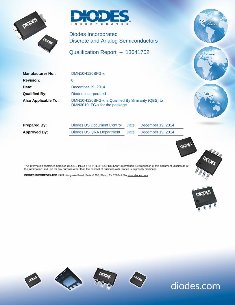
Diodes Incorporated Discrete and Analog Semiconductors
Qualification Report – 13041702
Manufacturer No.: DMN10H120SFG-x
Revision: 0
Date: December 19, 2014
Qualified By: Diodes Incorporated
Also Applicable To: DMN10H120SFG-x is Qualified By Similarity (QBS) to DMN3010LFG-x for the package.
Prepared By: Diodes US Document Control Date December 19, 2014
Approved By: Diodes US QRA Department Date December 19, 2014
The information contained herein is DIODES INCORPORATED PROPRIETARY information. Reproduction of this document, disclosure of the information, and use for any purpose other than the conduct of business with Diodes is expressly prohibited DIODES INCORPORATED 4949 Hedgcoxe Road, Suite # 200, Plano, TX 75024 USA www.diodes.com
Quality and Reliability Data Notice Plastic encapsulated Diodes Incorporated semiconductor devices are not designed and are not warranted to be suitable for use in some military applications and/or military environments. Use of plastic encapsulated Diodes Incorporated semiconductor devices in military applications and/or military environments, in lieu of hermetically sealed ceramic devices, is understood to be fully at the risk of Buyer. Quality and reliability data provided by Diodes Incorporated is intended to be an estimate of product performance based upon history only. It does not imply that any performance levels reflected in such data can be met if the product is operated outside the conditions expressly stated in the latest published data sheet for a device. Existing industry standards for plastic encapsulated microcircuit qualification and reliability monitors are based upon historical data, experiments, and field experience with the use of these devices in commercial and industrial applications. The applicability of these standards in determining the suitability for use and safety performance in life support, military and aerospace applications has not been established. Due to the multiple variations in field operating conditions, a component manufacturer can only base estimates of product life on models and the results of package and die level qualification. The buyer’s use of this data, and all consequences of such use, is solely the buyer’s responsibility. Buyer assumes full responsibility to perform sufficient engineering and additional qualification testing in order to properly evaluate the buyer’s application and determine whether a candidate device is suitable for use in that application. The information provided by Diodes Incorporated shall not be considered sufficient grounds on which to base any such determination. THIS INFORMATION IS PROVIDED "AS IS" WITHOUT ANY EXPRESS OR IMPLIED WARRANTY OF ANY KIND INCLUDING WARRANTIES OF MERCHANTABILITY, NONINFRINGEMENT OF INTELLECTUAL PROPERTY, OR FITNESS FOR ANY PARTICULAR PURPOSE. IN NO EVENT SHALL DIODES INCORPORATEDOR ITS SUPPLIERS BE LIABLE FOR ANY DAMAGES WHATSOEVER (INCLUDING, WITHOUT LIMITATION, DAMAGES FOR LOSS OF PROFITS, BUSINESS INTERRUPTION, LOSS OF INFORMATION) ARISING OUT OF THE USE OF OR INABILITY TO USE THE INFORMATION, EVEN IF DIODES INCORPORATED HAS BEEN ADVISED OF THE POSSIBILITY OF SUCH DAMAGES. Diodes Incorporated may provide technical, applications or design advice, quality characterization, and reliability data or service providing these items shall not expand or otherwise affect Diodes Incorporated warranties as set forth in the Diodes Incorporated Standard Terms and Conditions of Sale for and no obligation or liability shall arise from Diodes Incorporated provision of such items.
"The information contained herein is DIODES INCORPORATED PROPRIETARY information. Reproduction of this document, disclosure of the information, and use for any purpose other than the conduct of business with Diodes
Incorporated is expressly prohibited".
DIODES INCORPORATED 4949 Hedgcoxe Road, Suite # 200
Plano, TX 75024 USA (972) 987-3900
www.diodes.com
DMN10H120SFG
AD
VA
NC
E I
NF
OR
MA
TIO
N
100V N-CHANNEL ENHANCEMENT MODE MOSFET POWERDI®
Product Summary
V(BR)DSS RDS(ON) max ID max
TA = +25°C
100V 110mΩ @ VGS = 10V 3.8 A
122mΩ @ VGS = 6.0V 3.6 A
Description This MOSFET is designed to minimize the on-state resistance (RDS(on)) and yet maintain superior switching performance, making it ideal for high efficiency power management applications.
Applications • Power Management Functions • DC-DC Converters
Features and Benefits • Low RDS(ON) – ensures on state losses are minimized • Small form factor thermally efficient package enables higher
density end products • Occupies just 33% of the board area occupied by SO-8 enabling
smaller end product • Totally Lead-Free & Fully RoHS Compliant (Notes 1 & 2) • Halogen and Antimony Free. “Green” Device (Note 3) • Qualified to AEC-Q101 Standards for High Reliability
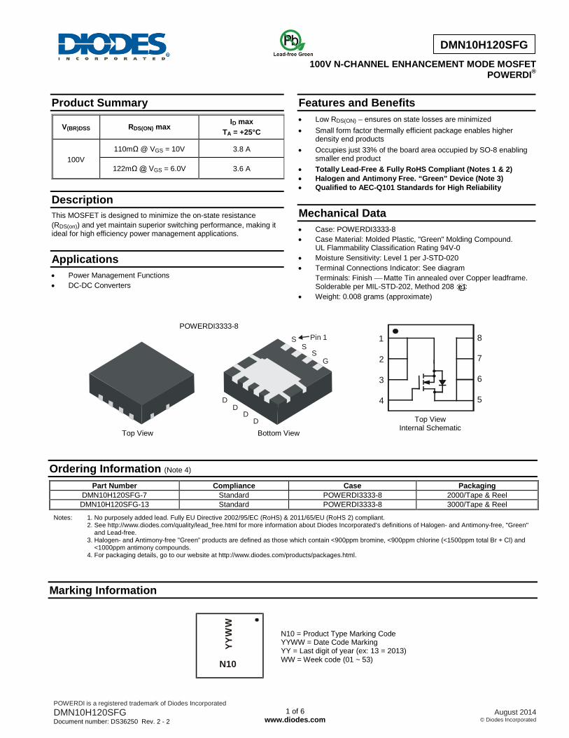
Mechanical Data • Case: POWERDI3333-8 • Case Material: Molded Plastic, "Green" Molding Compound.
UL Flammability Classification Rating 94V-0 • Moisture Sensitivity: Level 1 per J-STD-020 • Terminal Connections Indicator: See diagram
Terminals: Finish Matte Tin annealed over Copper leadframe. Solderable per MIL-STD-202, Method 208
• Weight: 0.008 grams (approximate)
Ordering Information (Note 4)
Part Number Compliance Case Packaging DMN10H120SFG-7 Standard POWERDI3333-8 2000/Tape & Reel DMN10H120SFG-13 Standard POWERDI3333-8 3000/Tape & Reel
Notes: 1. No purposely added lead. Fully EU Directive 2002/95/EC (RoHS) & 2011/65/EU (RoHS 2) compliant. 2. See http://www.diodes.com/quality/lead_free.html for more information about Diodes Incorporated’s definitions of Halogen- and Antimony-free, "Green" and Lead-free. 3. Halogen- and Antimony-free "Green” products are defined as those which contain <900ppm bromine, <900ppm chlorine (<1500ppm total Br + Cl) and <1000ppm antimony compounds. 4. For packaging details, go to our website at http://www.diodes.com/products/packages.html.
Marking Information
Bottom View
SS
SG
DD
DD
Pin 1
Top View
N10 = Product Type Marking Code YYWW = Date Code Marking YY = Last digit of year (ex: 13 = 2013) WW = Week code (01 ~ 53)
POWERDI3333-8
1
2
3
4
8
7
6
5
Top View Internal Schematic
N10
Y Y W
W
POWERDI is a registered trademark of Diodes Incorporated DMN10H120SFG Document number: DS36250 Rev. 2 - 2
1 of 6 www.diodes.com
August 2014 © Diodes Incorporated
DMN10H120SFG
AD
VA
NC
E I
NF
OR
MA
TIO
N
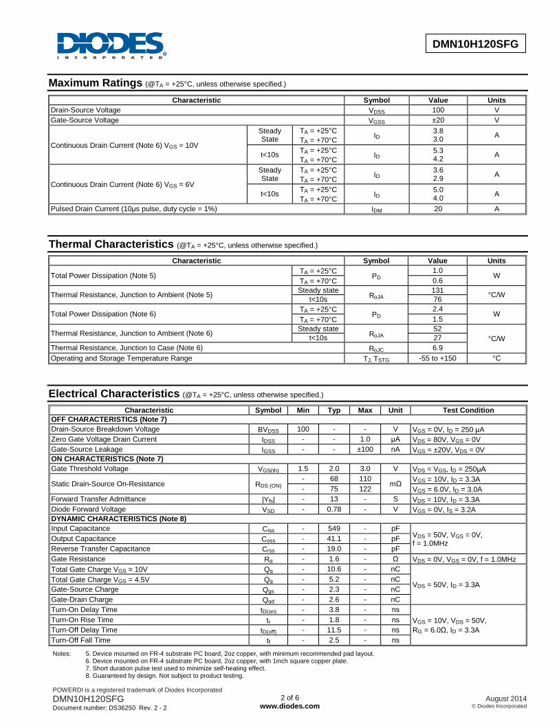
Maximum Ratings (@TA = +25°C, unless otherwise specified.)
Characteristic Symbol Value Units Drain-Source Voltage VDSS 100 V Gate-Source Voltage VGSS ±20 V
Continuous Drain Current (Note 6) VGS = 10V
Steady State
TA = +25°C TA = +70°C ID 3.8
3.0 A
t<10s TA = +25°C TA = +70°C ID 5.3
4.2 A
Continuous Drain Current (Note 6) VGS = 6V
Steady State
TA = +25°C TA = +70°C ID 3.6
2.9 A
t<10s TA = +25°C TA = +70°C ID 5.0
4.0 A
Pulsed Drain Current (10μs pulse, duty cycle = 1%) IDM 20 A
Thermal Characteristics (@TA = +25°C, unless otherwise specified.)
Characteristic Symbol Value Units
Total Power Dissipation (Note 5) TA = +25°C PD
1.0 W
TA = +70°C 0.6
Thermal Resistance, Junction to Ambient (Note 5) Steady state RθJA
131 °C/W t<10s 76
Total Power Dissipation (Note 6) TA = +25°C PD
2.4 W
TA = +70°C 1.5
Thermal Resistance, Junction to Ambient (Note 6) Steady state RθJA
52 °C/W
t<10s 27
Thermal Resistance, Junction to Case (Note 6) RθJC 6.9 Operating and Storage Temperature Range TJ, TSTG -55 to +150 °C
Electrical Characteristics (@TA = +25°C, unless otherwise specified.)
Characteristic Symbol Min Typ Max Unit Test Condition OFF CHARACTERISTICS (Note 7) Drain-Source Breakdown Voltage BVDSS 100 - - V VGS = 0V, ID = 250 μA Zero Gate Voltage Drain Current IDSS - - 1.0 μA VDS = 80V, VGS = 0V Gate-Source Leakage IGSS - - ±100 nA VGS = ±20V, VDS = 0V ON CHARACTERISTICS (Note 7) Gate Threshold Voltage VGS(th) 1.5 2.0 3.0 V VDS = VGS, ID = 250μA
Static Drain-Source On-Resistance RDS (ON) - 68 110
mΩ VGS = 10V, ID = 3.3A - 75 122 VGS = 6.0V, ID = 3.0A
Forward Transfer Admittance |Yfs| - 13 - S VDS = 10V, ID = 3.3A Diode Forward Voltage VSD - 0.78 - V VGS = 0V, IS = 3.2A DYNAMIC CHARACTERISTICS (Note 8) Input Capacitance Ciss - 549 - pF
VDS = 50V, VGS = 0V, f = 1.0MHz Output Capacitance Coss - 41.1 - pF
Reverse Transfer Capacitance Crss - 19.0 - pF Gate Resistance Rg - 1.6 - Ω VDS = 0V, VGS = 0V, f = 1.0MHz Total Gate Charge VGS = 10V Qg - 10.6 - nC
VDS = 50V, ID = 3.3A Total Gate Charge VGS = 4.5V Qg - 5.2 - nC Gate-Source Charge Qgs - 2.3 - nC Gate-Drain Charge Qgd - 2.6 - nC Turn-On Delay Time tD(on) - 3.8 - ns
VGS = 10V, VDS = 50V, RG = 6.0Ω, ID = 3.3A
Turn-On Rise Time tr - 1.8 - ns Turn-Off Delay Time tD(off) - 11.5 - ns Turn-Off Fall Time tf - 2.5 - ns
Notes: 5. Device mounted on FR-4 substrate PC board, 2oz copper, with minimum recommended pad layout. 6. Device mounted on FR-4 substrate PC board, 2oz copper, with 1inch square copper plate. 7. Short duration pulse test used to minimize self-heating effect. 8. Guaranteed by design. Not subject to product testing.
POWERDI is a registered trademark of Diodes Incorporated DMN10H120SFG Document number: DS36250 Rev. 2 - 2
2 of 6 www.diodes.com
August 2014 © Diodes Incorporated
DMN10H120SFG
AD
VA
NC
E I
NF
OR
MA
TIO
N
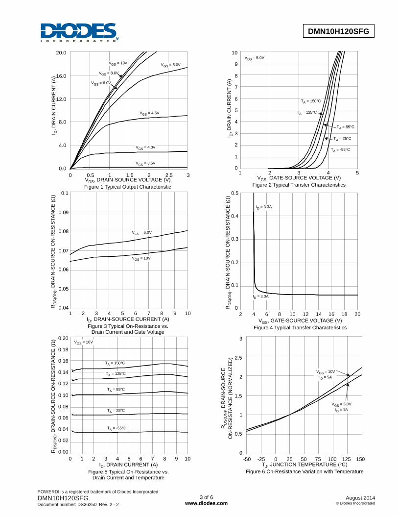
0.0
4.0
8.0
12.0
16.0
20.0
0 0.5 1 1.5 2 2.5 3V , DRAIN-SOURCE VOLTAGE (V)Figure 1 Typical Output Characteristic
DS
I, D
RA
IN C
UR
RE
NT
(A)
D
V = 3.5VGS
V = 10VGS
V = 4.0VGS
V = 4.5VGS
V = 5.0VGS
V = 8.0VGS
V = 6.0VGS
0
1
2
3
4
5
6
7
8
9
10
1 2 3 4 5V , GATE-SOURCE VOLTAGE (V)GS
Figure 2 Typical Transfer Characteristics
I, D
RA
IN C
UR
RE
NT
(A)
D
T = 150°CA
T = 125°CA
T = 85°CA
T = 25°CA
T = -55°CA
V = 5.0VDS
0.04
0.05
0.06
0.07
0.08
0.09
0.1
1 2 3 4 5 6 7 8 9 10I , DRAIN-SOURCE CURRENT (A)D Figure 3 Typical On-Resistance vs.
Drain Current and Gate Voltage
R, D
RA
IN-S
OU
RC
E O
N-R
ES
ISTA
NC
E (
)D
S(O
N)
Ω
V = 6.0VGS
V = 10VGS
0
0.1
0.2
0.3
0.4
0.5
2 4 6 8 10 12 14 16 18 20V , GATE-SOURCE VOLTAGE (V)GS
Figure 4 Typical Transfer Characteristics
R, D
RA
IN-S
OU
RC
E O
N-R
ES
ISTA
NC
E (
)D
S(O
N)
Ω
I = 3.3AD
I = 3.0AD
0.00
0.02
0.04
0.06
0.08
0.10
0.12
0.14
0.16
0.18
0.20
0 1 2 3 4 5 6 7 8 9 10I , DRAIN CURRENT (A)D
Figure 5 Typical On-Resistance vs. Drain Current and Temperature
R, D
RAI
N-S
OU
RC
E O
N-R
ES
ISTA
NC
E (
)D
S(O
N)
Ω
T = -55°CA
T = 25°CA
T = 85°CA
T = 125°CA
T = 150°CA
V = 10VGS
0
0.5
1
1.5
2
2.5
3
-50 -25 0 25 50 75 100 125 150T , JUNCTION TEMPERATURE ( C)
Figure 6 On-Resistance Variation with TemperatureJ °
R, D
RA
IN-S
OU
RC
E
ON
-RE
SIS
TAN
CE
(NO
RM
ALI
ZED
)D
S(O
N)
V = VI = 1A
GS
D
5.0
V = VI = 5AGS
D
10
POWERDI is a registered trademark of Diodes Incorporated DMN10H120SFG Document number: DS36250 Rev. 2 - 2
3 of 6 www.diodes.com
August 2014 © Diodes Incorporated
DMN10H120SFG
AD
VA
NC
E I
NF
OR
MA
TIO
N
0
0.03
0.06
0.09
0.12
0.15
0.18
-50 -25 0 25 50 75 100 125 150T , JUNCTION TEMPERATURE ( C)
Figure 7 On-Resistance Variation with TemperatureJ °
R, D
RA
IN-S
OU
RC
E O
N-R
ES
ISTA
NC
E (
)D
S(O
N)
Ω
V = VI = 1AGS
D
5
V = VI = 5AGS
D
10
1
1.5
2
2.5
3
3.5
-50 -25 0 25 50 75 100 125 150T , JUNCTION TEMPERATURE ( C)
Figure 8 Gate Threshold Variation vs. Ambient TemperatureJ °
I = 1mAD
I = 250µAD
V, G
ATE
TH
RE
SH
OLD
VO
LTA
GE
(V)
GS
(th)
0
1
2
3
4
5
6
7
8
9
10
0 0.3 0.6 0.9 1.2 1.5V , SOURCE-DRAIN VOLTAGE (V)SD
Figure 9 Diode Forward Voltage vs. Current
I, S
OU
RC
E C
UR
RE
NT
(A)
S
T = 150°CA
T = 125°CAT = 85°CA
T = 25°CA
T = -55°CA
10
100
1000
0 5 10 15 20 25 30 35 40 45 50V , DRAIN-SOURCE VOLTAGE (V)DS
Figure 10 Typical Junction Capacitance
C, J
UN
CTI
ON
CA
PAC
ITA
NC
E (p
F)T
Ciss
Coss
Crss
f = 1MHz
0
2
4
6
8
10
0 2 4 6 8 10 12Q (nC)g, TOTAL GATE CHARGE
Figure 11 Gate Charge
V G
ATE
TH
RES
HO
LD V
OLT
AG
E (V
)G
S
V = 50VI = A
DS
D
3.3
0.001
0.01
0.1
1
10
100
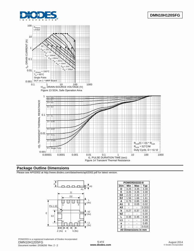
0.1 1 10 100 1000-V , DRAIN-SOURCE VOLTAGE (V)Figure 12 SOA, Safe Operation Area
DS
-I, D
RA
IN C
UR
RE
NT
(A)
D
RLimited
DS(on)
DCP = 10sW
P = 1sWP = 100msW
P = 10msW
P = 1msWP = 100µsWT = 150°C
T = 25°CJ(max)
ASingle PulseDUT on 1 * MRP Board
P = 20msW
P = 60msW
POWERDI is a registered trademark of Diodes Incorporated DMN10H120SFG Document number: DS36250 Rev. 2 - 2
4 of 6 www.diodes.com
August 2014 © Diodes Incorporated
DMN10H120SFG
AD
VA
NC
E I
NF
OR
MA
TIO
N
Package Outline Dimensions Please see AP02002 at http://www.diodes.com/datasheets/ap02002.pdf for latest version.
0.001
0.01
0.1
1
10
100
0.1 1 10 100 1000
RLimited
DS(on)
DC
P = 10sWP = 1sWP = 100msW
P = 10msW P = 1msW
P = 100µsW
-V , DRAIN-SOURCE VOLTAGE (V)Figure 13 SOA, Safe Operation Area
DS
-I, D
RA
IN C
UR
RE
NT
(A)
D
T = 150°CT = 60°C
J(max)
ASingle PulseDUT on 1 * MRP Board
P = 60msWP = 20msW
0.001
0.01
0.1
1
0.00001 0.0001 0.001 0.01 0.1 1 10 100 1000t1, PULSE DURATION TIME (sec)
Figure 14 Transient Thermal Resistance
r(t),
TR
AN
SIE
NT
THE
RM
AL
RE
SIS
TAN
CE
D = 0.5D = 0.7D = 0.9
D = 0.3
D = 0.1
D = 0.05
D = 0.02
D = 0.01
D = 0.005
D = Single Pulse
R (t) = r(t) * RR = 52°C/WDuty Cycle, D = t1/ t2
θ θ
θ
JA JA
JA
POWERDI3333-8 Dim Min Max Typ
D 3.25 3.35 3.30 E 3.25 3.35 3.30
D2 2.22 2.32 2.27 E2 1.56 1.66 1.61 A 0.75 0.85 0.80 A1 0 0.05 0.02 A3 − − 0.203 b 0.27 0.37 0.32
b2 − − 0.20 L 0.35 0.45 0.40
L1 − − 0.39 e − − 0.65 Z − − 0.515 All Dimensions in mm
A
A1A3
D
D2
EE2
b2(4x)
L(4x)
L1(3x)
b (8x)eZ (4x)
Pin 1 ID 1 4
8 5
POWERDI is a registered trademark of Diodes Incorporated DMN10H120SFG Document number: DS36250 Rev. 2 - 2
5 of 6 www.diodes.com
August 2014 © Diodes Incorporated
DMN10H120SFG
AD
VA
NC
E I
NF
OR
MA
TIO
N
Suggested Pad Layout Please see AP02001 at http://www.diodes.com/datasheets/ap02001.pdf for the latest version.
IMPORTANT NOTICE DIODES INCORPORATED MAKES NO WARRANTY OF ANY KIND, EXPRESS OR IMPLIED, WITH REGARDS TO THIS DOCUMENT, INCLUDING, BUT NOT LIMITED TO, THE IMPLIED WARRANTIES OF MERCHANTABILITY AND FITNESS FOR A PARTICULAR PURPOSE (AND THEIR EQUIVALENTS UNDER THE LAWS OF ANY JURISDICTION). Diodes Incorporated and its subsidiaries reserve the right to make modifications, enhancements, improvements, corrections or other changes without further notice to this document and any product described herein. Diodes Incorporated does not assume any liability arising out of the application or use of this document or any product described herein; neither does Diodes Incorporated convey any license under its patent or trademark rights, nor the rights of others. Any Customer or user of this document or products described herein in such applications shall assume all risks of such use and will agree to hold Diodes Incorporated and all the companies whose products are represented on Diodes Incorporated website, harmless against all damages. Diodes Incorporated does not warrant or accept any liability whatsoever in respect of any products purchased through unauthorized sales channel. Should Customers purchase or use Diodes Incorporated products for any unintended or unauthorized application, Customers shall indemnify and hold Diodes Incorporated and its representatives harmless against all claims, damages, expenses, and attorney fees arising out of, directly or indirectly, any claim of personal injury or death associated with such unintended or unauthorized application. Products described herein may be covered by one or more United States, international or foreign patents pending. Product names and markings noted herein may also be covered by one or more United States, international or foreign trademarks. This document is written in English but may be translated into multiple languages for reference. Only the English version of this document is the final and determinative format released by Diodes Incorporated.
LIFE SUPPORT Diodes Incorporated products are specifically not authorized for use as critical components in life support devices or systems without the express written approval of the Chief Executive Officer of Diodes Incorporated. As used herein: A. Life support devices or systems are devices or systems which: 1. are intended to implant into the body, or
2. support or sustain life and whose failure to perform when properly used in accordance with instructions for use provided in the labeling can be reasonably expected to result in significant injury to the user.
B. A critical component is any component in a life support device or system whose failure to perform can be reasonably expected to cause the failure of the life support device or to affect its safety or effectiveness. Customers represent that they have all necessary expertise in the safety and regulatory ramifications of their life support devices or systems, and acknowledge and agree that they are solely responsible for all legal, regulatory and safety-related requirements concerning their products and any use of Diodes Incorporated products in such safety-critical, life support devices or systems, notwithstanding any devices- or systems-related information or support that may be provided by Diodes Incorporated. Further, Customers must fully indemnify Diodes Incorporated and its representatives against any damages arising out of the use of Diodes Incorporated products in such safety-critical, life support devices or systems. Copyright © 2014, Diodes Incorporated www.diodes.com
Dimensions Value (in mm) C 0.650 G 0.230
G1 0.420 Y 3.700
Y1 2.250 Y2 1.850 Y3 0.700 X 2.370
X2 0.420
X
Y
Y1
Y3
Y2
X2 C
1 4
8 5
G
G1
POWERDI is a registered trademark of Diodes Incorporated DMN10H120SFG Document number: DS36250 Rev. 2 - 2
6 of 6 www.diodes.com
August 2014 © Diodes Incorporated
CERTIFICATE OF DESIGN AND CONSTRUCTION
Printed specifications are not controlled documents. Verify revision before using.
Page 1 of 1 DIC-074 R2 Diodes Incorporated Rel Date: 6/25/2013 www.diodes.com
Assembly and Test Site
DIODES INC Glass Transition Temperature (TG)
135°C
DIC P/N DMN10H120SFG-7 DMN10H120SFG-13 Lead Frame Type PowerDI3333-8L E type
Package Type PowerDI3333-8L Lead Frame Manufacturer MSMM
DIE P/N AL921BXX (MLM) / ALA43CXX (full mask) Lead Frame Material A194
Die Line or Process MOSFET Terminal Finish (Plating) Material
PPF(NiPdAu), Finish plating: Pb free (Sn)
Wafer Diameter 8 inch Header Plating (Die Land Area) PPF Plate
Wafer Fab Site(s) Sumpro Max Junction Temperature (Tj) 150°C
ID Method (multiple sites)
N/A Max Thermal Resistance Junction to Case (θJC)
6.9°C/W
Assembly Locations(s)
Shanghai Kaihong Electronic Co., Ltd. No.999 Chenchun Road, Xinqiao Town, Songjiang,Shanghai,P.R. China 201612 DIODES INC. IN SHANGHAI, Plant1,NO.111-10 Songjiang Export Processing Zone, Shanghai,P.R.China 201600
Max Thermal Resistance Junction to Ambient (θJA)*
55°C/W
Test Locations(s) DIODES INC. IN SHANGHAI, Plant1,NO.111-10 Songjiang Export Processing Zone, Shanghai,P.R.China 201600
Front Metal Type (Top Layer) AlCu
Die attach Method / Material
Epoxy/84-1LMISR4 Front Metal Thickness (Top Layer)
4um
Bond Wire/Clip Material & Wire Diameter
Cu 1.7mil Back Metal Type (All Layers) Ti/Ni/Ti/Ag
Bond Type (at top side of the die)
Thermo sonic Back Metal Thickness (all Layers)
1KA/3KA/100A/10KA
Bond Type (at leadframe)
Thermo sonic Die Conformal Coating (Passivation)
oxide
No. of Bonds over Active Area
Gate: 1wire; Source: 12wires; Die Passivation Thickness
Range TEOS oxide 1.6K/SIN3.8K
Mold Compound Material Type
EME-G770HCD Die Size (Width x Length x Thickness) in mm
2.24*0.98*0.158mm
Mold Compound Material Manufacturer
SUMITOMO No. of Mask Steps 6
Completed by Date Certified by Date
Typed/Printed Creafe cheng July 31, 2013 Bill Tian July 31, 2013
Signature Creafe cheng July 31, 2013 Bill Tian July 31, 2013
Title MOSFET PE Discrete Manager
DW-008 (AECQ101) Test# Test Description Test Conditions #Lots #To Test Results REMARKS
7.3.2 (1) PRE- AND POST- STRESS ELECTRICALTEST (TEST) Per Spec
7.3.3 (2) PRECONDITIONING (PC) JSED22 A-113 N/A for Axial 1 308 N/A7.3.5.1 (3) EXTERNAL VISUAL (EV) MIL-STD-750 METHOD 2071 1 154 0/154
7.3.5.2 (4) PARAMETRIC VERIFICATION (PV) 1 of 3 25 0/25
Lot #2 2 of 3 25 N/A
Lot #3 3 of 3 25 N/A
7.3.5.3 FORWARD SURGE MIL-750D, Method 4066 1 45 N/A7.3.5.4 (5) HIGH TEMP. REVERSE BIAS (HTRB) T=150 Vd=80V, PER JESD22 A-108
Pretest 1 77 0/77 @ 500 Hours T=150 Vd=80V, PER JESD22 A-108 1 77 0/77 Final 1000 Hours T=150 Vd=80V, PER JESD22 A-108 1 77 0/77
(6) HIGH TEMP GATE BIAS (HTGB) T=150 Vg=20V, PER JESD22 A-108 Pretest 1 77 0/77 @ 500 Hours T=150 Vg=20V, PER JESD22 A-108 1 77 0/77 Final 1000 Hours T=150 Vg=20V, PER JESD22 A-108 1 77 0/77
7.3.5.5 (7) TEMPERATURE CYCLING (TC) T=-65-150, PER JESD22 A-104 1 77 N/A7.3.5.6 (8) AUTOCLAVE (AC) T=121 15PSIG 100%RH 1 77 N/A
7.3.5.7 (9-1) Highly Accelerated Stress Test(HAST) T=130 RH=85% Vd=80V 1 77 N/A7.3.5.7 (9-2) High Humidity High Temp. Reverse Bias(H3TRB) T=85 RH=85% Vd=80V 1 77 N/A
7.3.5.8 (10) INTERMITTENTOPERATING LIFE (IOL) Vd=5V / Id=160mA; PER MIL-STD-750 METHOD 1037 1 77 N/A 2mins on/off
(10a) POWER AND TEMP. CYCLE (PTC) JESD22 A-105, Per Table AEC-Q101, p11 1 77 N/A
7.3.5.9 (11) ESD CHARACTERIZATION (ESD) PER AEC-Q101-001 & -002 1 60 pass MM=400VHBM=800V
7.3.5.10 (12) D.P.A. (DPA) AEC Q101-004 SEC. 4 1 6 N/A7.3.5.11 (13) PHYSICAL DIMENSION (PD) PER JESD22 B-100 1 30 N/A7.3.5.12 (14) TERMINAL STRENGTH (TS) MIL-STD-750, Method 2036 1 30 N/A7.3.5.13 (15) RESISTANCE TO SOLVENTS (RTS) JESD22 B-107 1 30 N/A
(16) CONSTANT ACCELERATION (CA) N/A, not hermetically sealed device. N/A N/A(17) VIBRATION VARIABLE FREQUENCY (VVF) N/A, not hermetically sealed device. N/A N/A(18) MECHANICAL SHOCK (MS) N/A, not hermetically sealed device. N/A N/A(19) HERMETICITY (HER) N/A, not hermetically sealed device. N/A N/A
7.3.5.14 (20) RESISTANCE TO SOLDER HEAT (RSH) JESD22 B-106 1 30 N/A [email protected] (21) SOLDERABILITY (SD) J-STD-002 1 10 N/A [email protected] (22) THERMAL RESISTANCE (TR) JESD 24-3, 24-4, 24-6 as appropriate 1 10 0/107.3.5.17 (23) WIRE BOND STRENGTH (WBS) MIL-STD-750 METHOD 2037 1 25 N/A7.3.5.18 (24) BOND SHEAR (BS) AEC-Q101-003 1 25 N/A7.3.5.19 (25) DIE SHEAR (DS) MIL-STD-750 METHOD 2017 1 25 N/A
(26) UNCLAMPED INDUCTIVE SWITCHING (UIS) N/A, not for Diode N/A N/A(27) DIELECTRIC INTEGRITY (DI) N/A, not for Diode N/A N/A
Q-Form Q014-4,Rev.K
Package Description : POWERDI3333-8
CUSTOMER:
DIODES INC.:
SHANGHAI KAIHONG ELECTRONIC CO.,LTD
Reliability Test SummaryFACTORY: PART NUMBER : DMN10H120SFG SWR1303335
Summary: The lot passed 1000hrs HTRB/HTGB tests.
Submitted by: Jianhua Yang 6/7/13
LABORATORY (If Different): PART DESCRIPTION : Qualification for Sumpro wafer: AL821DXX(1.7 Cu wire+ EME-G770HCD).
Approved by: Adam Gu 6/7/13
Per Data SheetTa1=-55, Ta2=25, Ta3=85, Ta4=150Characteristic BVDSS@VGS=0V, ID=250uACharacteristic IDSS@VDS=80V, VGS=0VCharacteristic IGSS@VGS=±20V, VDS=0VCharacteristic VGS(th)@VDS=VGS, ID=250uACharacteristic RDSON@VGS=10V, ID=3.3ACharacteristic RDSON@VGS=6V, ID=3.0ACharacteristic yFS@VDS=10V,ID=3.3A
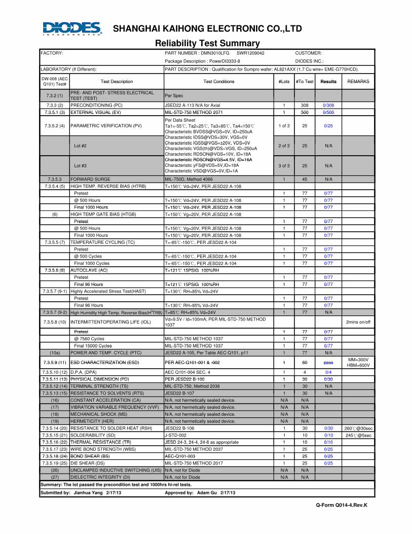
SHANGHAI KAIHONG ELECTRONIC CO.,LTD
CUSTOMER:
Reliability Test SummaryFACTORY: PART NUMBER : DMN3010LFG SWR1209042
LABORATORY (If Different): PART DESCRIPTION : Qualification for Sumpro wafer: AL821AXX (1.7 Cu wire+ EME-G770HCD).
Package Description : PowerDI3333-8
CUSTOMER:
DIODES INC.:
FACTORY: PART NUMBER : DMN3010LFG SWR1209042
DW-008 (AEC
Q101) Test#Test Description Test Conditions #Lots #To Test Results REMARKS
LABORATORY (If Different): PART DESCRIPTION : Qualification for Sumpro wafer: AL821AXX (1.7 Cu wire+ EME-G770HCD).
Q101) Test#Test Description Test Conditions #Lots #To Test Results REMARKS
7.3.2 (1)PRE- AND POST- STRESS ELECTRICAL
TEST (TEST)Per Spec7.3.2 (1)
TEST (TEST)Per Spec
7.3.3 (2) PRECONDITIONING (PC) JSED22 A-113 N/A for Axial 1 308 0/308
7.3.5.1 (3) EXTERNAL VISUAL (EV) MIL-STD-750 METHOD 2071 1 500 0/5007.3.5.1 (3) EXTERNAL VISUAL (EV) MIL-STD-750 METHOD 2071 1 500 0/500
7.3.5.2 (4) PARAMETRIC VERIFICATION (PV) 1 of 3 25 0/25
Per Data Sheet
Ta1=-55, Ta2=25, Ta3=85, Ta4=150
Characteristic BVDSS@VGS=0V, ID=250uA
Lot #2 2 of 3 25 N/A
Ta1=-55 , Ta2=25 , Ta3=85 , Ta4=150
Characteristic BVDSS@VGS=0V, ID=250uA
Characteristic IDSS@VDS=30V, VGS=0V
Characteristic IGSS@VGS=±20V, VDS=0V Lot #2 2 of 3 25 N/A
Characteristic IGSS@VGS=±20V, VDS=0V
Characteristic VGS(th)@VDS=VGS, ID=250uA
Characteristic RDSON@VGS=10V, ID=18A
Characteristic RDSON@VGS=4.5V, ID=16A
Lot #3 3 of 3 25 N/A
Characteristic RDSON@VGS=4.5V, ID=16A
Characteristic yFS@VDS=5V,ID=18A
Characteristic VSD@VGS=0V,ID=1A
7.3.5.3 FORWARD SURGE MIL-750D, Method 4066 1 45 N/A
7.3.5.4 (5) HIGH TEMP. REVERSE BIAS (HTRB) T=150 Vd=24V, PER JESD22 A-108
Pretest 1 77 0/77 Pretest 1 77 0/77
@ 500 Hours T=150 Vd=24V, PER JESD22 A-108 1 77 0/77
Final 1000 Hours T=150 Vd=24V, PER JESD22 A-108 1 77 0/77 Final 1000 Hours T=150 Vd=24V, PER JESD22 A-108 1 77 0/77
(6) HIGH TEMP GATE BIAS (HTGB) T=150 Vg=20V, PER JESD22 A-108
Pretest 1 77 0/77 Pretest 1 77 0/77
@ 500 Hours T=150 Vg=20V, PER JESD22 A-108 1 77 0/77
Final 1000 Hours T=150 Vg=20V, PER JESD22 A-108 1 77 0/77 Final 1000 Hours T=150 Vg=20V, PER JESD22 A-108 1 77 0/77
7.3.5.5 (7) TEMPERATURE CYCLING (TC) T=-65-150, PER JESD22 A-104
Pretest 1 77 0/77
@ 500 Cycles T=-65-150, PER JESD22 A-104 1 77 0/77 @ 500 Cycles T=-65-150, PER JESD22 A-104 1 77 0/77
Final 1000 Cycles T=-65-150, PER JESD22 A-104 1 77 0/77
7.3.5.6 (8) AUTOCLAVE (AC) T=121 15PSIG 100%RH7.3.5.6 (8) AUTOCLAVE (AC) T=121 15PSIG 100%RH
Pretest 1 77 0/77
Final 96 Hours T=121 15PSIG 100%RH 1 77 0/77 Final 96 Hours T=121 15PSIG 100%RH 1 77 0/77
7.3.5.7 (9-1) Highly Accelerated Stress Test(HAST) T=130 RH=85% Vd=24V
Pretest 1 77 0/77 Pretest 1 77 0/77
Final 96 Hours T=130 RH=85% Vd=24V 1 77 0/77
7.3.5.7 (9-2) High Humidity High Temp. Reverse Bias(H3TRB) T=85 RH=85% Vd=24V 1 77 N/A
7.3.5.8 (10) INTERMITTENTOPERATING LIFE (IOL)Vd=9.5V / Id=100mA; PER MIL-STD-750 METHOD
10372mins on/off
Pretest 1 77 0/77 Pretest 1 77 0/77
@ 7560 Cycles MIL-STD-750 METHOD 1037 1 77 0/77
Final 15000 Cycles MIL-STD-750 METHOD 1037 1 77 0/77 Final 15000 Cycles MIL-STD-750 METHOD 1037 1 77 0/77
(10a) POWER AND TEMP. CYCLE (PTC) JESD22 A-105, Per Table AEC-Q101, p11 1 77 N/A
7.3.5.9 (11) ESD CHARACTERIZATION (ESD) PER AEC-Q101-001 & -002 1 60 passMM=300V
HBM=600V7.3.5.9 (11) ESD CHARACTERIZATION (ESD) PER AEC-Q101-001 & -002 1 60 pass
HBM=600V
7.3.5.10 (12) D.P.A. (DPA) AEC Q101-004 SEC. 4 1 4 0/4
7.3.5.11 (13) PHYSICAL DIMENSION (PD) PER JESD22 B-100 1 30 0/307.3.5.11 (13) PHYSICAL DIMENSION (PD) PER JESD22 B-100 1 30 0/30
7.3.5.12 (14) TERMINAL STRENGTH (TS) MIL-STD-750, Method 2036 1 30 N/A
7.3.5.13 (15) RESISTANCE TO SOLVENTS (RTS) JESD22 B-107 1 30 N/A7.3.5.13 (15) RESISTANCE TO SOLVENTS (RTS) JESD22 B-107 1 30 N/A
(16) CONSTANT ACCELERATION (CA) N/A, not hermetically sealed device. N/A N/A
(17) VIBRATION VARIABLE FREQUENCY (VVF) N/A, not hermetically sealed device. N/A N/A(17) VIBRATION VARIABLE FREQUENCY (VVF) N/A, not hermetically sealed device. N/A N/A
(18) MECHANICAL SHOCK (MS) N/A, not hermetically sealed device. N/A N/A
(19) HERMETICITY (HER) N/A, not hermetically sealed device. N/A N/A
7.3.5.14 (20) RESISTANCE TO SOLDER HEAT (RSH) JESD22 B-106 1 30 0/307.3.5.14 (20) RESISTANCE TO SOLDER HEAT (RSH) JESD22 B-106 1 30 0/30 260@30sec
7.3.5.15 (21) SOLDERABILITY (SD) J-STD-002 1 10 0/10 245@5sec
7.3.5.16 (22) THERMAL RESISTANCE (TR) JESD 24-3, 24-4, 24-6 as appropriate 1 10 0/107.3.5.16 (22) THERMAL RESISTANCE (TR) JESD 24-3, 24-4, 24-6 as appropriate 1 10 0/10
7.3.5.17 (23) WIRE BOND STRENGTH (WBS) MIL-STD-750 METHOD 2037 1 25 0/25
7.3.5.18 (24) BOND SHEAR (BS) AEC-Q101-003 1 25 0/257.3.5.18 (24) BOND SHEAR (BS) AEC-Q101-003 1 25 0/25
7.3.5.19 (25) DIE SHEAR (DS) MIL-STD-750 METHOD 2017 1 25 0/25
(26) UNCLAMPED INDUCTIVE SWITCHING (UIS) N/A, not for Diode N/A N/A(26) UNCLAMPED INDUCTIVE SWITCHING (UIS) N/A, not for Diode N/A N/A
(27) DIELECTRIC INTEGRITY (DI) N/A, not for Diode N/A N/A
Summary: The lot passed the precondition test and 1000hrs hi-rel tests.
Q-Form Q014-4,Rev.K
Submitted by: Jianhua Yang 2/17/13 Approved by: Adam Gu 2/17/13
Q-Form Q014-4,Rev.K
![DYNAMICS OF A DISCRETE-TIME STOICHIOMETRIC ...hwang/DiscreteOptimalForaging.pdfstoichiometric optimal foraging model [15] with its discrete-time analog. We study the discrete-time](https://img.pdfslide.net/doc/110x75/60c2e22ddd4f9278ff1214c6/dynamics-of-a-discrete-time-stoichiometric-hwangdiscreteoptimalforagingpdf.jpg)