Embed Size (px)
Citation preview

3501
0516
00
Quantum with Unity ProDiscrete and Analog I/OReference Manual eng June 2005

2

Document Set
Document Set
Presentation This package contains the following manuals:Quantum Hardware Reference ManualQuantum Discrete and Analog I/O Reference ManualQuantum Experts and Communication Reference ManualGrounding and Electromagnetic Compatibility of PLC Systems User ManualQuantum Series 800 I/O Reference Manual
3

Document Set
4

Table of Contents
Safety Information . . . . . . . . . . . . . . . . . . . . . . . . . . . . . . . . . . . 17
About the Book . . . . . . . . . . . . . . . . . . . . . . . . . . . . . . . . . . . . . .19
Part I General Information . . . . . . . . . . . . . . . . . . . . . . . . . . . . . 23At a Glance . . . . . . . . . . . . . . . . . . . . . . . . . . . . . . . . . . . . . . . . . . . . . . . . . . . . . 23
Chapter 1 Configuration of the module. . . . . . . . . . . . . . . . . . . . . . . . . . .25Overview . . . . . . . . . . . . . . . . . . . . . . . . . . . . . . . . . . . . . . . . . . . . . . . . . . . . . . . 25Mapping a Local Quantum I/O Station . . . . . . . . . . . . . . . . . . . . . . . . . . . . . . . . 26Open the Parameter Configuration . . . . . . . . . . . . . . . . . . . . . . . . . . . . . . . . . . . 27
Chapter 2 Quantum Addressing Modes. . . . . . . . . . . . . . . . . . . . . . . . . . .29Overview . . . . . . . . . . . . . . . . . . . . . . . . . . . . . . . . . . . . . . . . . . . . . . . . . . . . . . . 29Flat Addressing . . . . . . . . . . . . . . . . . . . . . . . . . . . . . . . . . . . . . . . . . . . . . . . . . . 30Topological Addressing. . . . . . . . . . . . . . . . . . . . . . . . . . . . . . . . . . . . . . . . . . . . 31IODDT Addressing . . . . . . . . . . . . . . . . . . . . . . . . . . . . . . . . . . . . . . . . . . . . . . . 32Quantum IODDTs . . . . . . . . . . . . . . . . . . . . . . . . . . . . . . . . . . . . . . . . . . . . . . . . 33Addressing Example . . . . . . . . . . . . . . . . . . . . . . . . . . . . . . . . . . . . . . . . . . . . . . 35Discrete I/O Bit Numbering . . . . . . . . . . . . . . . . . . . . . . . . . . . . . . . . . . . . . . . . . 36I/O Modules Status Byte . . . . . . . . . . . . . . . . . . . . . . . . . . . . . . . . . . . . . . . . . . . 37I/O Configuration for Discrete Input Modules . . . . . . . . . . . . . . . . . . . . . . . . . . . 40I/O Configuration for Discrete Output Modules . . . . . . . . . . . . . . . . . . . . . . . . . . 46I/O Configuration for Discrete Input/Output Modules . . . . . . . . . . . . . . . . . . . . . 53
Part II Analog IN Modules . . . . . . . . . . . . . . . . . . . . . . . . . . . . . . 57At a Glance . . . . . . . . . . . . . . . . . . . . . . . . . . . . . . . . . . . . . . . . . . . . . . . . . . . . . 57
Chapter 3 140 ACI 030 00: Analog Current / Voltage IN Module . . . . . . . 59Overview . . . . . . . . . . . . . . . . . . . . . . . . . . . . . . . . . . . . . . . . . . . . . . . . . . . . . . . 59Presentation . . . . . . . . . . . . . . . . . . . . . . . . . . . . . . . . . . . . . . . . . . . . . . . . . . . . 60Indicators. . . . . . . . . . . . . . . . . . . . . . . . . . . . . . . . . . . . . . . . . . . . . . . . . . . . . . . 61Wiring Diagram . . . . . . . . . . . . . . . . . . . . . . . . . . . . . . . . . . . . . . . . . . . . . . . . . . 62Specifications . . . . . . . . . . . . . . . . . . . . . . . . . . . . . . . . . . . . . . . . . . . . . . . . . . . 64Addressing . . . . . . . . . . . . . . . . . . . . . . . . . . . . . . . . . . . . . . . . . . . . . . . . . . . . . 66
5

Parameter Configuration . . . . . . . . . . . . . . . . . . . . . . . . . . . . . . . . . . . . . . . . . . . 68
Chapter 4 140 ACI 040 00: Analog Mixed Current IN Module . . . . . . . . . 69Overview . . . . . . . . . . . . . . . . . . . . . . . . . . . . . . . . . . . . . . . . . . . . . . . . . . . . . . . 69Presentation. . . . . . . . . . . . . . . . . . . . . . . . . . . . . . . . . . . . . . . . . . . . . . . . . . . . . 70Indicators . . . . . . . . . . . . . . . . . . . . . . . . . . . . . . . . . . . . . . . . . . . . . . . . . . . . . . . 71Wiring Diagram . . . . . . . . . . . . . . . . . . . . . . . . . . . . . . . . . . . . . . . . . . . . . . . . . . 72Specifications. . . . . . . . . . . . . . . . . . . . . . . . . . . . . . . . . . . . . . . . . . . . . . . . . . . . 74Addressing. . . . . . . . . . . . . . . . . . . . . . . . . . . . . . . . . . . . . . . . . . . . . . . . . . . . . . 76Parameter Configuration . . . . . . . . . . . . . . . . . . . . . . . . . . . . . . . . . . . . . . . . . . . 78
Chapter 5 140 ARI 030 10: Analog RTD IN Module . . . . . . . . . . . . . . . . . 79Overview . . . . . . . . . . . . . . . . . . . . . . . . . . . . . . . . . . . . . . . . . . . . . . . . . . . . . . . 79Presentation. . . . . . . . . . . . . . . . . . . . . . . . . . . . . . . . . . . . . . . . . . . . . . . . . . . . . 80Indicators . . . . . . . . . . . . . . . . . . . . . . . . . . . . . . . . . . . . . . . . . . . . . . . . . . . . . . . 81Wiring Diagram . . . . . . . . . . . . . . . . . . . . . . . . . . . . . . . . . . . . . . . . . . . . . . . . . . 82140 ARI 030 10 Specifications. . . . . . . . . . . . . . . . . . . . . . . . . . . . . . . . . . . . . . . 84Addressing. . . . . . . . . . . . . . . . . . . . . . . . . . . . . . . . . . . . . . . . . . . . . . . . . . . . . . 86Parameter Configuration . . . . . . . . . . . . . . . . . . . . . . . . . . . . . . . . . . . . . . . . . . . 88
Chapter 6 140 ATI 030 00: Analog TC IN Module . . . . . . . . . . . . . . . . . . . 91Overview . . . . . . . . . . . . . . . . . . . . . . . . . . . . . . . . . . . . . . . . . . . . . . . . . . . . . . . 91Presentation. . . . . . . . . . . . . . . . . . . . . . . . . . . . . . . . . . . . . . . . . . . . . . . . . . . . . 92Indicators . . . . . . . . . . . . . . . . . . . . . . . . . . . . . . . . . . . . . . . . . . . . . . . . . . . . . . . 93Wiring Diagram . . . . . . . . . . . . . . . . . . . . . . . . . . . . . . . . . . . . . . . . . . . . . . . . . . 94Specifications. . . . . . . . . . . . . . . . . . . . . . . . . . . . . . . . . . . . . . . . . . . . . . . . . . . . 96Addressing. . . . . . . . . . . . . . . . . . . . . . . . . . . . . . . . . . . . . . . . . . . . . . . . . . . . . . 98Parameter Configuration . . . . . . . . . . . . . . . . . . . . . . . . . . . . . . . . . . . . . . . . . . 101
Chapter 7 140 AVI 030 00: Analog Mixed Current/Voltage IN Module . 103Overview . . . . . . . . . . . . . . . . . . . . . . . . . . . . . . . . . . . . . . . . . . . . . . . . . . . . . . 103Presentation. . . . . . . . . . . . . . . . . . . . . . . . . . . . . . . . . . . . . . . . . . . . . . . . . . . . 104Indicators . . . . . . . . . . . . . . . . . . . . . . . . . . . . . . . . . . . . . . . . . . . . . . . . . . . . . . 105Wiring Diagram . . . . . . . . . . . . . . . . . . . . . . . . . . . . . . . . . . . . . . . . . . . . . . . . . 106Specifications. . . . . . . . . . . . . . . . . . . . . . . . . . . . . . . . . . . . . . . . . . . . . . . . . . . 108Addressing. . . . . . . . . . . . . . . . . . . . . . . . . . . . . . . . . . . . . . . . . . . . . . . . . . . . . 111Parameter Configuration . . . . . . . . . . . . . . . . . . . . . . . . . . . . . . . . . . . . . . . . . . 113
Part III Analog OUT Modules . . . . . . . . . . . . . . . . . . . . . . . . . . . 115At a Glance . . . . . . . . . . . . . . . . . . . . . . . . . . . . . . . . . . . . . . . . . . . . . . . . . . . . 115
Chapter 8 140 ACO 020 00: Analog Current OUT Module . . . . . . . . . . . 117Overview . . . . . . . . . . . . . . . . . . . . . . . . . . . . . . . . . . . . . . . . . . . . . . . . . . . . . . 117Presentation. . . . . . . . . . . . . . . . . . . . . . . . . . . . . . . . . . . . . . . . . . . . . . . . . . . . 118Indicators . . . . . . . . . . . . . . . . . . . . . . . . . . . . . . . . . . . . . . . . . . . . . . . . . . . . . . 119Wiring Diagram . . . . . . . . . . . . . . . . . . . . . . . . . . . . . . . . . . . . . . . . . . . . . . . . . 120
6

Specifications . . . . . . . . . . . . . . . . . . . . . . . . . . . . . . . . . . . . . . . . . . . . . . . . . . 122Addressing . . . . . . . . . . . . . . . . . . . . . . . . . . . . . . . . . . . . . . . . . . . . . . . . . . . . 124Parameter Configuration . . . . . . . . . . . . . . . . . . . . . . . . . . . . . . . . . . . . . . . . . . 125
Chapter 9 140 ACO 130 00: Analog Mixed Current OUT Module . . . . . . 127Overview . . . . . . . . . . . . . . . . . . . . . . . . . . . . . . . . . . . . . . . . . . . . . . . . . . . . . . 127Presentation . . . . . . . . . . . . . . . . . . . . . . . . . . . . . . . . . . . . . . . . . . . . . . . . . . . 128Indicators. . . . . . . . . . . . . . . . . . . . . . . . . . . . . . . . . . . . . . . . . . . . . . . . . . . . . . 129Wiring Diagram . . . . . . . . . . . . . . . . . . . . . . . . . . . . . . . . . . . . . . . . . . . . . . . . . 130Specifications . . . . . . . . . . . . . . . . . . . . . . . . . . . . . . . . . . . . . . . . . . . . . . . . . . 132Addressing . . . . . . . . . . . . . . . . . . . . . . . . . . . . . . . . . . . . . . . . . . . . . . . . . . . . 134Parameter Configuration . . . . . . . . . . . . . . . . . . . . . . . . . . . . . . . . . . . . . . . . . . 135
Chapter 10 140 AVO 020 00: Analog Mixed Voltage OUT Module . . . . . . 137Overview . . . . . . . . . . . . . . . . . . . . . . . . . . . . . . . . . . . . . . . . . . . . . . . . . . . . . . 137Presentation . . . . . . . . . . . . . . . . . . . . . . . . . . . . . . . . . . . . . . . . . . . . . . . . . . . 138Indicators. . . . . . . . . . . . . . . . . . . . . . . . . . . . . . . . . . . . . . . . . . . . . . . . . . . . . . 139Wiring Diagram . . . . . . . . . . . . . . . . . . . . . . . . . . . . . . . . . . . . . . . . . . . . . . . . . 140Specifications . . . . . . . . . . . . . . . . . . . . . . . . . . . . . . . . . . . . . . . . . . . . . . . . . . 142Addressing . . . . . . . . . . . . . . . . . . . . . . . . . . . . . . . . . . . . . . . . . . . . . . . . . . . . 144Parameter Configuration . . . . . . . . . . . . . . . . . . . . . . . . . . . . . . . . . . . . . . . . . . 145
Part IV Analog IN / OUT Modules . . . . . . . . . . . . . . . . . . . . . . . 147At a Glance . . . . . . . . . . . . . . . . . . . . . . . . . . . . . . . . . . . . . . . . . . . . . . . . . . . . 147
Chapter 11 140 AMM 090 00: Analog Mixed Current/Voltage IN / OUT Module . . . . . . . . . . . . . . . . . . . . . . . . . . . . . . . . . . . . . . . . . . . . 149Overview . . . . . . . . . . . . . . . . . . . . . . . . . . . . . . . . . . . . . . . . . . . . . . . . . . . . . . 149Presentation . . . . . . . . . . . . . . . . . . . . . . . . . . . . . . . . . . . . . . . . . . . . . . . . . . . 150Indicators. . . . . . . . . . . . . . . . . . . . . . . . . . . . . . . . . . . . . . . . . . . . . . . . . . . . . . 151Wiring Diagram . . . . . . . . . . . . . . . . . . . . . . . . . . . . . . . . . . . . . . . . . . . . . . . . . 152Specifications . . . . . . . . . . . . . . . . . . . . . . . . . . . . . . . . . . . . . . . . . . . . . . . . . . 154Addressing . . . . . . . . . . . . . . . . . . . . . . . . . . . . . . . . . . . . . . . . . . . . . . . . . . . . 157Parameter Configuration . . . . . . . . . . . . . . . . . . . . . . . . . . . . . . . . . . . . . . . . . . 160
Part V Discrete IN Modules . . . . . . . . . . . . . . . . . . . . . . . . . . . . 163At a Glance . . . . . . . . . . . . . . . . . . . . . . . . . . . . . . . . . . . . . . . . . . . . . . . . . . . . 163
Chapter 12 General Information . . . . . . . . . . . . . . . . . . . . . . . . . . . . . . . . . 165Discrete I/O Logic Circuits. . . . . . . . . . . . . . . . . . . . . . . . . . . . . . . . . . . . . . . . . 165
Chapter 13 140 DDI 153 10: 5 VDC 4x8 TTL Source IN Module . . . . . . .167Overview . . . . . . . . . . . . . . . . . . . . . . . . . . . . . . . . . . . . . . . . . . . . . . . . . . . . . . 167Presentation . . . . . . . . . . . . . . . . . . . . . . . . . . . . . . . . . . . . . . . . . . . . . . . . . . . 168Indicators. . . . . . . . . . . . . . . . . . . . . . . . . . . . . . . . . . . . . . . . . . . . . . . . . . . . . . 169Wiring Diagram . . . . . . . . . . . . . . . . . . . . . . . . . . . . . . . . . . . . . . . . . . . . . . . . . 170
7

Specifications. . . . . . . . . . . . . . . . . . . . . . . . . . . . . . . . . . . . . . . . . . . . . . . . . . . 172Parameter Configuration . . . . . . . . . . . . . . . . . . . . . . . . . . . . . . . . . . . . . . . . . . 174
Chapter 14 140 DDI 353 00: 24 VDC 4x8 Sink IN Module . . . . . . . . . . . . . 175Overview . . . . . . . . . . . . . . . . . . . . . . . . . . . . . . . . . . . . . . . . . . . . . . . . . . . . . . 175Presentation. . . . . . . . . . . . . . . . . . . . . . . . . . . . . . . . . . . . . . . . . . . . . . . . . . . . 176Indicators . . . . . . . . . . . . . . . . . . . . . . . . . . . . . . . . . . . . . . . . . . . . . . . . . . . . . . 177Wiring Diagram . . . . . . . . . . . . . . . . . . . . . . . . . . . . . . . . . . . . . . . . . . . . . . . . . 178Specifications. . . . . . . . . . . . . . . . . . . . . . . . . . . . . . . . . . . . . . . . . . . . . . . . . . . 180Parameter Configuration . . . . . . . . . . . . . . . . . . . . . . . . . . . . . . . . . . . . . . . . . . 182
Chapter 15 140 DDI 353 10: 24 VDC 4x8 Source IN Module . . . . . . . . . . 183Overview . . . . . . . . . . . . . . . . . . . . . . . . . . . . . . . . . . . . . . . . . . . . . . . . . . . . . . 183Presentation. . . . . . . . . . . . . . . . . . . . . . . . . . . . . . . . . . . . . . . . . . . . . . . . . . . . 184Indicators . . . . . . . . . . . . . . . . . . . . . . . . . . . . . . . . . . . . . . . . . . . . . . . . . . . . . . 185Wiring Diagram . . . . . . . . . . . . . . . . . . . . . . . . . . . . . . . . . . . . . . . . . . . . . . . . . 186Specifications. . . . . . . . . . . . . . . . . . . . . . . . . . . . . . . . . . . . . . . . . . . . . . . . . . . 188Parameter Configuration . . . . . . . . . . . . . . . . . . . . . . . . . . . . . . . . . . . . . . . . . . 190
Chapter 16 140 DDI 364 00: 24 VDC 6x16 Telefast IN Module . . . . . . . . . 191Overview . . . . . . . . . . . . . . . . . . . . . . . . . . . . . . . . . . . . . . . . . . . . . . . . . . . . . . 191Presentation. . . . . . . . . . . . . . . . . . . . . . . . . . . . . . . . . . . . . . . . . . . . . . . . . . . . 192Indicators . . . . . . . . . . . . . . . . . . . . . . . . . . . . . . . . . . . . . . . . . . . . . . . . . . . . . . 195Color Codes. . . . . . . . . . . . . . . . . . . . . . . . . . . . . . . . . . . . . . . . . . . . . . . . . . . . 196Specifications . . . . . . . . . . . . . . . . . . . . . . . . . . . . . . . . . . . . . . . . . . . . . . . . . . 197Parameter Configuration . . . . . . . . . . . . . . . . . . . . . . . . . . . . . . . . . . . . . . . . . . 198
Chapter 17 140 DDI 673 00: 125 VDC 3x8 Sink IN Module . . . . . . . . . . . . 199Overview . . . . . . . . . . . . . . . . . . . . . . . . . . . . . . . . . . . . . . . . . . . . . . . . . . . . . . 199Presentation. . . . . . . . . . . . . . . . . . . . . . . . . . . . . . . . . . . . . . . . . . . . . . . . . . . . 200Indicators . . . . . . . . . . . . . . . . . . . . . . . . . . . . . . . . . . . . . . . . . . . . . . . . . . . . . . 201Wiring Diagram . . . . . . . . . . . . . . . . . . . . . . . . . . . . . . . . . . . . . . . . . . . . . . . . . 202Specifications. . . . . . . . . . . . . . . . . . . . . . . . . . . . . . . . . . . . . . . . . . . . . . . . . . . 204Parameter Configuration . . . . . . . . . . . . . . . . . . . . . . . . . . . . . . . . . . . . . . . . . . 207
Chapter 18 140 DDI 841 00: 10 ... 60 VDC 8x2 Sink IN Module . . . . . . . . 209Overview . . . . . . . . . . . . . . . . . . . . . . . . . . . . . . . . . . . . . . . . . . . . . . . . . . . . . . 209Presentation. . . . . . . . . . . . . . . . . . . . . . . . . . . . . . . . . . . . . . . . . . . . . . . . . . . . 210Indicators . . . . . . . . . . . . . . . . . . . . . . . . . . . . . . . . . . . . . . . . . . . . . . . . . . . . . . 211Wiring Diagram . . . . . . . . . . . . . . . . . . . . . . . . . . . . . . . . . . . . . . . . . . . . . . . . . 212Specifications. . . . . . . . . . . . . . . . . . . . . . . . . . . . . . . . . . . . . . . . . . . . . . . . . . . 214Parameter Configuration . . . . . . . . . . . . . . . . . . . . . . . . . . . . . . . . . . . . . . . . . . 216
Chapter 19 140 DDI 853 00: 10 ... 60 VDC 4x8 Sink IN Module . . . . . . . . 217Overview . . . . . . . . . . . . . . . . . . . . . . . . . . . . . . . . . . . . . . . . . . . . . . . . . . . . . . 217Presentation. . . . . . . . . . . . . . . . . . . . . . . . . . . . . . . . . . . . . . . . . . . . . . . . . . . . 218Indicators . . . . . . . . . . . . . . . . . . . . . . . . . . . . . . . . . . . . . . . . . . . . . . . . . . . . . . 219
8

Wiring Diagram . . . . . . . . . . . . . . . . . . . . . . . . . . . . . . . . . . . . . . . . . . . . . . . . . 220Specifications . . . . . . . . . . . . . . . . . . . . . . . . . . . . . . . . . . . . . . . . . . . . . . . . . . 222Parameter Configuration . . . . . . . . . . . . . . . . . . . . . . . . . . . . . . . . . . . . . . . . . . 224
Chapter 20 140 DAI 340 00: 24 VAC 16x1 IN Module. . . . . . . . . . . . . . . . . 225Overview . . . . . . . . . . . . . . . . . . . . . . . . . . . . . . . . . . . . . . . . . . . . . . . . . . . . . . 225Presentation . . . . . . . . . . . . . . . . . . . . . . . . . . . . . . . . . . . . . . . . . . . . . . . . . . . 226Indicators. . . . . . . . . . . . . . . . . . . . . . . . . . . . . . . . . . . . . . . . . . . . . . . . . . . . . . 227Wiring Diagram . . . . . . . . . . . . . . . . . . . . . . . . . . . . . . . . . . . . . . . . . . . . . . . . . 228Specifications . . . . . . . . . . . . . . . . . . . . . . . . . . . . . . . . . . . . . . . . . . . . . . . . . . 230Parameter Configuration . . . . . . . . . . . . . . . . . . . . . . . . . . . . . . . . . . . . . . . . . . 232
Chapter 21 140 DAI 353 00: 24 VAC 4x8 IN Module. . . . . . . . . . . . . . . . . . 233Overview . . . . . . . . . . . . . . . . . . . . . . . . . . . . . . . . . . . . . . . . . . . . . . . . . . . . . . 233Presentation . . . . . . . . . . . . . . . . . . . . . . . . . . . . . . . . . . . . . . . . . . . . . . . . . . . 234Indicators. . . . . . . . . . . . . . . . . . . . . . . . . . . . . . . . . . . . . . . . . . . . . . . . . . . . . . 235Wiring Diagram . . . . . . . . . . . . . . . . . . . . . . . . . . . . . . . . . . . . . . . . . . . . . . . . . 236Specifications . . . . . . . . . . . . . . . . . . . . . . . . . . . . . . . . . . . . . . . . . . . . . . . . . . 238Parameter Configuration . . . . . . . . . . . . . . . . . . . . . . . . . . . . . . . . . . . . . . . . . . 240
Chapter 22 140 DAI 440 00: 48 VAC 16x1 IN Module. . . . . . . . . . . . . . . . . 241Overview . . . . . . . . . . . . . . . . . . . . . . . . . . . . . . . . . . . . . . . . . . . . . . . . . . . . . . 241Presentation . . . . . . . . . . . . . . . . . . . . . . . . . . . . . . . . . . . . . . . . . . . . . . . . . . . 242Indicators. . . . . . . . . . . . . . . . . . . . . . . . . . . . . . . . . . . . . . . . . . . . . . . . . . . . . . 243Wiring Diagram . . . . . . . . . . . . . . . . . . . . . . . . . . . . . . . . . . . . . . . . . . . . . . . . . 244Specifications . . . . . . . . . . . . . . . . . . . . . . . . . . . . . . . . . . . . . . . . . . . . . . . . . . 246Parameter Configuration . . . . . . . . . . . . . . . . . . . . . . . . . . . . . . . . . . . . . . . . . . 248
Chapter 23 140 DAI 453 00: 48 VAC 4x8 IN Module. . . . . . . . . . . . . . . . . . 249Overview . . . . . . . . . . . . . . . . . . . . . . . . . . . . . . . . . . . . . . . . . . . . . . . . . . . . . . 249Presentation . . . . . . . . . . . . . . . . . . . . . . . . . . . . . . . . . . . . . . . . . . . . . . . . . . . 250Indicators. . . . . . . . . . . . . . . . . . . . . . . . . . . . . . . . . . . . . . . . . . . . . . . . . . . . . . 251Wiring Diagram . . . . . . . . . . . . . . . . . . . . . . . . . . . . . . . . . . . . . . . . . . . . . . . . . 252Specifications . . . . . . . . . . . . . . . . . . . . . . . . . . . . . . . . . . . . . . . . . . . . . . . . . . 254Parameter Configuration . . . . . . . . . . . . . . . . . . . . . . . . . . . . . . . . . . . . . . . . . . 256
Chapter 24 140 DAI 540 00: 115 VAC 16x1 IN Module. . . . . . . . . . . . . . . .257Overview . . . . . . . . . . . . . . . . . . . . . . . . . . . . . . . . . . . . . . . . . . . . . . . . . . . . . . 257Presentation . . . . . . . . . . . . . . . . . . . . . . . . . . . . . . . . . . . . . . . . . . . . . . . . . . . 258Indicators. . . . . . . . . . . . . . . . . . . . . . . . . . . . . . . . . . . . . . . . . . . . . . . . . . . . . . 259Wiring Diagram . . . . . . . . . . . . . . . . . . . . . . . . . . . . . . . . . . . . . . . . . . . . . . . . . 260Specifications . . . . . . . . . . . . . . . . . . . . . . . . . . . . . . . . . . . . . . . . . . . . . . . . . . 262Parameter Configuration . . . . . . . . . . . . . . . . . . . . . . . . . . . . . . . . . . . . . . . . . . 264
Chapter 25 140 DAI 543 00: 115 VAC 2x8 IN Module. . . . . . . . . . . . . . . . . 265Overview . . . . . . . . . . . . . . . . . . . . . . . . . . . . . . . . . . . . . . . . . . . . . . . . . . . . . . 265Presentation . . . . . . . . . . . . . . . . . . . . . . . . . . . . . . . . . . . . . . . . . . . . . . . . . . . 266
9

Indicators . . . . . . . . . . . . . . . . . . . . . . . . . . . . . . . . . . . . . . . . . . . . . . . . . . . . . . 267Wiring Diagram . . . . . . . . . . . . . . . . . . . . . . . . . . . . . . . . . . . . . . . . . . . . . . . . . 268Specifications. . . . . . . . . . . . . . . . . . . . . . . . . . . . . . . . . . . . . . . . . . . . . . . . . . . 270Parameter Configuration . . . . . . . . . . . . . . . . . . . . . . . . . . . . . . . . . . . . . . . . . . 272
Chapter 26 140 DAI 553 00: 115 VAC 4x8 IN Module . . . . . . . . . . . . . . . . 273Overview . . . . . . . . . . . . . . . . . . . . . . . . . . . . . . . . . . . . . . . . . . . . . . . . . . . . . . 273Presentation. . . . . . . . . . . . . . . . . . . . . . . . . . . . . . . . . . . . . . . . . . . . . . . . . . . . 274Indicators . . . . . . . . . . . . . . . . . . . . . . . . . . . . . . . . . . . . . . . . . . . . . . . . . . . . . . 275Wiring Diagram . . . . . . . . . . . . . . . . . . . . . . . . . . . . . . . . . . . . . . . . . . . . . . . . . 276Specifications. . . . . . . . . . . . . . . . . . . . . . . . . . . . . . . . . . . . . . . . . . . . . . . . . . . 278Parameter Configuration . . . . . . . . . . . . . . . . . . . . . . . . . . . . . . . . . . . . . . . . . . 280
Chapter 27 140 DAI 740 00: 230 VAC 16x1 IN Module . . . . . . . . . . . . . . . 281Overview . . . . . . . . . . . . . . . . . . . . . . . . . . . . . . . . . . . . . . . . . . . . . . . . . . . . . . 281Presentation. . . . . . . . . . . . . . . . . . . . . . . . . . . . . . . . . . . . . . . . . . . . . . . . . . . . 282Indicators . . . . . . . . . . . . . . . . . . . . . . . . . . . . . . . . . . . . . . . . . . . . . . . . . . . . . . 283Wiring Diagram . . . . . . . . . . . . . . . . . . . . . . . . . . . . . . . . . . . . . . . . . . . . . . . . . 284Specifications. . . . . . . . . . . . . . . . . . . . . . . . . . . . . . . . . . . . . . . . . . . . . . . . . . . 286Parameter Configuration . . . . . . . . . . . . . . . . . . . . . . . . . . . . . . . . . . . . . . . . . . 288
Chapter 28 140 DAI 753 00: 230 VAC 4x8 IN Module . . . . . . . . . . . . . . . . 289Overview . . . . . . . . . . . . . . . . . . . . . . . . . . . . . . . . . . . . . . . . . . . . . . . . . . . . . . 289Presentation. . . . . . . . . . . . . . . . . . . . . . . . . . . . . . . . . . . . . . . . . . . . . . . . . . . . 290Indicators . . . . . . . . . . . . . . . . . . . . . . . . . . . . . . . . . . . . . . . . . . . . . . . . . . . . . . 291Wiring Diagram . . . . . . . . . . . . . . . . . . . . . . . . . . . . . . . . . . . . . . . . . . . . . . . . . 292Specifications. . . . . . . . . . . . . . . . . . . . . . . . . . . . . . . . . . . . . . . . . . . . . . . . . . . 294Parameter Configuration . . . . . . . . . . . . . . . . . . . . . . . . . . . . . . . . . . . . . . . . . . 296
Chapter 29 140 DSI 353 00: 24 VDC 2x16 Supervised IN Module . . . . . . 297Overview . . . . . . . . . . . . . . . . . . . . . . . . . . . . . . . . . . . . . . . . . . . . . . . . . . . . . . 297Presentation. . . . . . . . . . . . . . . . . . . . . . . . . . . . . . . . . . . . . . . . . . . . . . . . . . . . 298Indicators . . . . . . . . . . . . . . . . . . . . . . . . . . . . . . . . . . . . . . . . . . . . . . . . . . . . . . 299Wiring Diagram . . . . . . . . . . . . . . . . . . . . . . . . . . . . . . . . . . . . . . . . . . . . . . . . . 300Specifications. . . . . . . . . . . . . . . . . . . . . . . . . . . . . . . . . . . . . . . . . . . . . . . . . . . 302Addressing. . . . . . . . . . . . . . . . . . . . . . . . . . . . . . . . . . . . . . . . . . . . . . . . . . . . . 303Parameter Configuration . . . . . . . . . . . . . . . . . . . . . . . . . . . . . . . . . . . . . . . . . . 305
Part VI Discrete OUT Modules . . . . . . . . . . . . . . . . . . . . . . . . . .307At a Glance . . . . . . . . . . . . . . . . . . . . . . . . . . . . . . . . . . . . . . . . . . . . . . . . . . . . 307
Chapter 30 General Information. . . . . . . . . . . . . . . . . . . . . . . . . . . . . . . . . 309Discrete I/O Logic Circuits . . . . . . . . . . . . . . . . . . . . . . . . . . . . . . . . . . . . . . . . . 309
Chapter 31 140 DDO 153 10: 5 VDC 4x8 TTL Sink OUT Module. . . . . . . 311Overview . . . . . . . . . . . . . . . . . . . . . . . . . . . . . . . . . . . . . . . . . . . . . . . . . . . . . . 311Presentation. . . . . . . . . . . . . . . . . . . . . . . . . . . . . . . . . . . . . . . . . . . . . . . . . . . . 312
10

Indicators. . . . . . . . . . . . . . . . . . . . . . . . . . . . . . . . . . . . . . . . . . . . . . . . . . . . . . 313Wiring Diagram . . . . . . . . . . . . . . . . . . . . . . . . . . . . . . . . . . . . . . . . . . . . . . . . . 314Specifications . . . . . . . . . . . . . . . . . . . . . . . . . . . . . . . . . . . . . . . . . . . . . . . . . . 316Maintenance . . . . . . . . . . . . . . . . . . . . . . . . . . . . . . . . . . . . . . . . . . . . . . . . . . . 317140 DDO 153 10 Parameter Configuration . . . . . . . . . . . . . . . . . . . . . . . . . . . . 318
Chapter 32 140 DDO 353 00: 24 VDC 4x8 Source OUT Module . . . . . . . .319Overview . . . . . . . . . . . . . . . . . . . . . . . . . . . . . . . . . . . . . . . . . . . . . . . . . . . . . . 319Presentation . . . . . . . . . . . . . . . . . . . . . . . . . . . . . . . . . . . . . . . . . . . . . . . . . . . 320Indicators. . . . . . . . . . . . . . . . . . . . . . . . . . . . . . . . . . . . . . . . . . . . . . . . . . . . . . 321Wiring Diagram . . . . . . . . . . . . . . . . . . . . . . . . . . . . . . . . . . . . . . . . . . . . . . . . . 322Specifications . . . . . . . . . . . . . . . . . . . . . . . . . . . . . . . . . . . . . . . . . . . . . . . . . . 324Maintenance . . . . . . . . . . . . . . . . . . . . . . . . . . . . . . . . . . . . . . . . . . . . . . . . . . . 326140 DDO 353 00 Parameter Configuration . . . . . . . . . . . . . . . . . . . . . . . . . . . . 327
Chapter 33 140 DDO 353 01: 24 VDC 4x8 Source OUT Module . . . . . . . .329Overview . . . . . . . . . . . . . . . . . . . . . . . . . . . . . . . . . . . . . . . . . . . . . . . . . . . . . . 329Presentation . . . . . . . . . . . . . . . . . . . . . . . . . . . . . . . . . . . . . . . . . . . . . . . . . . . 330Indicators. . . . . . . . . . . . . . . . . . . . . . . . . . . . . . . . . . . . . . . . . . . . . . . . . . . . . . 331Wiring Diagram . . . . . . . . . . . . . . . . . . . . . . . . . . . . . . . . . . . . . . . . . . . . . . . . . 332Specifications . . . . . . . . . . . . . . . . . . . . . . . . . . . . . . . . . . . . . . . . . . . . . . . . . . 334Maintenance . . . . . . . . . . . . . . . . . . . . . . . . . . . . . . . . . . . . . . . . . . . . . . . . . . . 336140 DDO 353 01 Parameter Configuration . . . . . . . . . . . . . . . . . . . . . . . . . . . . 337
Chapter 34 140 DDO 353 10: 24 VDC 4x8 Sink OUT Module . . . . . . . . . .339Overview . . . . . . . . . . . . . . . . . . . . . . . . . . . . . . . . . . . . . . . . . . . . . . . . . . . . . . 339Presentation . . . . . . . . . . . . . . . . . . . . . . . . . . . . . . . . . . . . . . . . . . . . . . . . . . . 340Indicators. . . . . . . . . . . . . . . . . . . . . . . . . . . . . . . . . . . . . . . . . . . . . . . . . . . . . . 341Wiring Diagram . . . . . . . . . . . . . . . . . . . . . . . . . . . . . . . . . . . . . . . . . . . . . . . . . 342Specifications . . . . . . . . . . . . . . . . . . . . . . . . . . . . . . . . . . . . . . . . . . . . . . . . . . 344Maintenance . . . . . . . . . . . . . . . . . . . . . . . . . . . . . . . . . . . . . . . . . . . . . . . . . . . 346140 DDO 353 10 Parameter Configuration . . . . . . . . . . . . . . . . . . . . . . . . . . . . 347
Chapter 35 140 DDO 364 00: 24 VDC 6x16 Telefast OUT Module . . . . . . 349Overview . . . . . . . . . . . . . . . . . . . . . . . . . . . . . . . . . . . . . . . . . . . . . . . . . . . . . . 349Presentation . . . . . . . . . . . . . . . . . . . . . . . . . . . . . . . . . . . . . . . . . . . . . . . . . . . 350Indicators. . . . . . . . . . . . . . . . . . . . . . . . . . . . . . . . . . . . . . . . . . . . . . . . . . . . . . 353140 DDO 364 00 Cable Color Codes . . . . . . . . . . . . . . . . . . . . . . . . . . . . . . . . 354Specifications . . . . . . . . . . . . . . . . . . . . . . . . . . . . . . . . . . . . . . . . . . . . . . . . . . 355140 DDO 364 00 Parameter Configuration . . . . . . . . . . . . . . . . . . . . . . . . . . . . 357
Chapter 36 140 DDO 843 00: 10 ... 60 VDC 2x8 Source OUT Module. . . .359Overview . . . . . . . . . . . . . . . . . . . . . . . . . . . . . . . . . . . . . . . . . . . . . . . . . . . . . . 359Presentation . . . . . . . . . . . . . . . . . . . . . . . . . . . . . . . . . . . . . . . . . . . . . . . . . . . 360Indicators. . . . . . . . . . . . . . . . . . . . . . . . . . . . . . . . . . . . . . . . . . . . . . . . . . . . . . 361Wiring Diagram . . . . . . . . . . . . . . . . . . . . . . . . . . . . . . . . . . . . . . . . . . . . . . . . . 362Specifications . . . . . . . . . . . . . . . . . . . . . . . . . . . . . . . . . . . . . . . . . . . . . . . . . . 363
11

Maintenance . . . . . . . . . . . . . . . . . . . . . . . . . . . . . . . . . . . . . . . . . . . . . . . . . . . 364140 DDO 843 00 Parameter Configuration . . . . . . . . . . . . . . . . . . . . . . . . . . . . 365
Chapter 37 140 DDO 885 00: 24 ... 125 VDC 2x6 Source OUT Module . . 367Overview . . . . . . . . . . . . . . . . . . . . . . . . . . . . . . . . . . . . . . . . . . . . . . . . . . . . . . 367Presentation. . . . . . . . . . . . . . . . . . . . . . . . . . . . . . . . . . . . . . . . . . . . . . . . . . . . 368Indicators . . . . . . . . . . . . . . . . . . . . . . . . . . . . . . . . . . . . . . . . . . . . . . . . . . . . . . 369Wiring Diagram . . . . . . . . . . . . . . . . . . . . . . . . . . . . . . . . . . . . . . . . . . . . . . . . . 370Specifications. . . . . . . . . . . . . . . . . . . . . . . . . . . . . . . . . . . . . . . . . . . . . . . . . . . 372Maintenance . . . . . . . . . . . . . . . . . . . . . . . . . . . . . . . . . . . . . . . . . . . . . . . . . . . 375140 DDO 885 00 Parameter Configuration . . . . . . . . . . . . . . . . . . . . . . . . . . . . 376
Chapter 38 140 DAO 840 00: 24 ... 230 VAC 16x1 OUT Module . . . . . . . . 379Overview . . . . . . . . . . . . . . . . . . . . . . . . . . . . . . . . . . . . . . . . . . . . . . . . . . . . . . 379Presentation. . . . . . . . . . . . . . . . . . . . . . . . . . . . . . . . . . . . . . . . . . . . . . . . . . . . 380Indicators . . . . . . . . . . . . . . . . . . . . . . . . . . . . . . . . . . . . . . . . . . . . . . . . . . . . . . 381Wiring Diagram . . . . . . . . . . . . . . . . . . . . . . . . . . . . . . . . . . . . . . . . . . . . . . . . . 382Specifications. . . . . . . . . . . . . . . . . . . . . . . . . . . . . . . . . . . . . . . . . . . . . . . . . . . 384140 DAO 840 00 Parameter Configuration . . . . . . . . . . . . . . . . . . . . . . . . . . . . 387
Chapter 39 140 DAO 840 10: 24 ... 115 VAC 16x1 OUT Module . . . . . . . . 389Overview . . . . . . . . . . . . . . . . . . . . . . . . . . . . . . . . . . . . . . . . . . . . . . . . . . . . . . 389Presentation. . . . . . . . . . . . . . . . . . . . . . . . . . . . . . . . . . . . . . . . . . . . . . . . . . . . 390Indicators . . . . . . . . . . . . . . . . . . . . . . . . . . . . . . . . . . . . . . . . . . . . . . . . . . . . . . 391Wiring Diagram . . . . . . . . . . . . . . . . . . . . . . . . . . . . . . . . . . . . . . . . . . . . . . . . . 392Specifications. . . . . . . . . . . . . . . . . . . . . . . . . . . . . . . . . . . . . . . . . . . . . . . . . . . 394140 DAO 840 10 Parameter Configuration . . . . . . . . . . . . . . . . . . . . . . . . . . . . 397
Chapter 40 140 DAO 842 10: 100 ... 230 VAC 4x4 OUT Module . . . . . . . . 399Overview . . . . . . . . . . . . . . . . . . . . . . . . . . . . . . . . . . . . . . . . . . . . . . . . . . . . . . 399Presentation. . . . . . . . . . . . . . . . . . . . . . . . . . . . . . . . . . . . . . . . . . . . . . . . . . . . 400Indicators . . . . . . . . . . . . . . . . . . . . . . . . . . . . . . . . . . . . . . . . . . . . . . . . . . . . . . 401Wiring Diagram . . . . . . . . . . . . . . . . . . . . . . . . . . . . . . . . . . . . . . . . . . . . . . . . . 402Specifications. . . . . . . . . . . . . . . . . . . . . . . . . . . . . . . . . . . . . . . . . . . . . . . . . . . 404Maintenance . . . . . . . . . . . . . . . . . . . . . . . . . . . . . . . . . . . . . . . . . . . . . . . . . . . 407140 DAO 842 10 Parameter Configuration . . . . . . . . . . . . . . . . . . . . . . . . . . . . 408
Chapter 41 140 DAO 842 20: 24 ... 48 VAC 4x4 OUT Module . . . . . . . . . . 409Overview . . . . . . . . . . . . . . . . . . . . . . . . . . . . . . . . . . . . . . . . . . . . . . . . . . . . . . 409Presentation. . . . . . . . . . . . . . . . . . . . . . . . . . . . . . . . . . . . . . . . . . . . . . . . . . . . 410Indicators . . . . . . . . . . . . . . . . . . . . . . . . . . . . . . . . . . . . . . . . . . . . . . . . . . . . . . 411Wiring Diagram . . . . . . . . . . . . . . . . . . . . . . . . . . . . . . . . . . . . . . . . . . . . . . . . . 412Specifications. . . . . . . . . . . . . . . . . . . . . . . . . . . . . . . . . . . . . . . . . . . . . . . . . . . 414Maintenance . . . . . . . . . . . . . . . . . . . . . . . . . . . . . . . . . . . . . . . . . . . . . . . . . . . 417140 DAO 842 20 Parameter Configuration . . . . . . . . . . . . . . . . . . . . . . . . . . . . 418
Chapter 42 140 DAO 853 00: 230 VAC 4x8 Source OUT Module. . . . . . . 419
12
Overview . . . . . . . . . . . . . . . . . . . . . . . . . . . . . . . . . . . . . . . . . . . . . . . . . . . . . . 419Presentation . . . . . . . . . . . . . . . . . . . . . . . . . . . . . . . . . . . . . . . . . . . . . . . . . . . 420Indicators. . . . . . . . . . . . . . . . . . . . . . . . . . . . . . . . . . . . . . . . . . . . . . . . . . . . . . 421Wiring Diagram . . . . . . . . . . . . . . . . . . . . . . . . . . . . . . . . . . . . . . . . . . . . . . . . . 422Specifications . . . . . . . . . . . . . . . . . . . . . . . . . . . . . . . . . . . . . . . . . . . . . . . . . . 424Maintenance . . . . . . . . . . . . . . . . . . . . . . . . . . . . . . . . . . . . . . . . . . . . . . . . . . . 427140 DAO 853 00 Parameter Configuration . . . . . . . . . . . . . . . . . . . . . . . . . . . . 428
Chapter 43 140 DRA 840 00: Relay 16x1 Normally Open OUT Module . .429Overview . . . . . . . . . . . . . . . . . . . . . . . . . . . . . . . . . . . . . . . . . . . . . . . . . . . . . . 429Presentation . . . . . . . . . . . . . . . . . . . . . . . . . . . . . . . . . . . . . . . . . . . . . . . . . . . 430Indicators. . . . . . . . . . . . . . . . . . . . . . . . . . . . . . . . . . . . . . . . . . . . . . . . . . . . . . 431Wiring Diagram . . . . . . . . . . . . . . . . . . . . . . . . . . . . . . . . . . . . . . . . . . . . . . . . . 432Specifications . . . . . . . . . . . . . . . . . . . . . . . . . . . . . . . . . . . . . . . . . . . . . . . . . . 434140 DRA 840 00 Parameter Configuration . . . . . . . . . . . . . . . . . . . . . . . . . . . . 436
Chapter 44 140 DRC 830 00: Relay 8x1 Normally Open / Normally Closed OUT Module. . . . . . . . . . . . . . . . . . . . . . . . . . . . . . . . . . . . . . . . 437Overview . . . . . . . . . . . . . . . . . . . . . . . . . . . . . . . . . . . . . . . . . . . . . . . . . . . . . . 437Presentation . . . . . . . . . . . . . . . . . . . . . . . . . . . . . . . . . . . . . . . . . . . . . . . . . . . 438Indicators. . . . . . . . . . . . . . . . . . . . . . . . . . . . . . . . . . . . . . . . . . . . . . . . . . . . . . 439Wiring Diagram . . . . . . . . . . . . . . . . . . . . . . . . . . . . . . . . . . . . . . . . . . . . . . . . . 440Specifications . . . . . . . . . . . . . . . . . . . . . . . . . . . . . . . . . . . . . . . . . . . . . . . . . . 442140 DRC 830 00 Parameter Configuration . . . . . . . . . . . . . . . . . . . . . . . . . . . . 445
Chapter 45 140 DVO 853 00: 10 ... 30 VDC 32x1 Verified OUT Module . . 447Overview . . . . . . . . . . . . . . . . . . . . . . . . . . . . . . . . . . . . . . . . . . . . . . . . . . . . . . 447Presentation . . . . . . . . . . . . . . . . . . . . . . . . . . . . . . . . . . . . . . . . . . . . . . . . . . . 448Indicators. . . . . . . . . . . . . . . . . . . . . . . . . . . . . . . . . . . . . . . . . . . . . . . . . . . . . . 449Wiring Diagram . . . . . . . . . . . . . . . . . . . . . . . . . . . . . . . . . . . . . . . . . . . . . . . . . 450Specifications . . . . . . . . . . . . . . . . . . . . . . . . . . . . . . . . . . . . . . . . . . . . . . . . . . 451Maintenance . . . . . . . . . . . . . . . . . . . . . . . . . . . . . . . . . . . . . . . . . . . . . . . . . . . 453Addressing . . . . . . . . . . . . . . . . . . . . . . . . . . . . . . . . . . . . . . . . . . . . . . . . . . . . 454Parameter Configuration . . . . . . . . . . . . . . . . . . . . . . . . . . . . . . . . . . . . . . . . . . 456
Part VII Discrete IN / OUT Modules . . . . . . . . . . . . . . . . . . . . . . 459At a Glance . . . . . . . . . . . . . . . . . . . . . . . . . . . . . . . . . . . . . . . . . . . . . . . . . . . . 459
Chapter 46 General Information . . . . . . . . . . . . . . . . . . . . . . . . . . . . . . . . . 461Discrete I/O Logic Circuits. . . . . . . . . . . . . . . . . . . . . . . . . . . . . . . . . . . . . . . . . 461
Chapter 47 140 DDM 390 00: 24 VDC 2x8 Sink IN / 2x4 Source OUT Module . . . . . . . . . . . . . . . . . . . . . . . . . . . . . . . . . . . . . . . . . . . 463Overview . . . . . . . . . . . . . . . . . . . . . . . . . . . . . . . . . . . . . . . . . . . . . . . . . . . . . . 463Presentation . . . . . . . . . . . . . . . . . . . . . . . . . . . . . . . . . . . . . . . . . . . . . . . . . . . 464Indicators. . . . . . . . . . . . . . . . . . . . . . . . . . . . . . . . . . . . . . . . . . . . . . . . . . . . . . 465
13

RIO Drop Location . . . . . . . . . . . . . . . . . . . . . . . . . . . . . . . . . . . . . . . . . . . . . . . 466Wiring Diagram . . . . . . . . . . . . . . . . . . . . . . . . . . . . . . . . . . . . . . . . . . . . . . . . . 467Specifications. . . . . . . . . . . . . . . . . . . . . . . . . . . . . . . . . . . . . . . . . . . . . . . . . . . 469Maintenance . . . . . . . . . . . . . . . . . . . . . . . . . . . . . . . . . . . . . . . . . . . . . . . . . . . 471140 DDM 390 00 Parameter Configuration . . . . . . . . . . . . . . . . . . . . . . . . . . . . 472
Chapter 48 140 DDM 690 00: 125 VDC High Power IN/OUT Module . . . . 475Overview . . . . . . . . . . . . . . . . . . . . . . . . . . . . . . . . . . . . . . . . . . . . . . . . . . . . . . 475Presentation. . . . . . . . . . . . . . . . . . . . . . . . . . . . . . . . . . . . . . . . . . . . . . . . . . . . 476Indicators . . . . . . . . . . . . . . . . . . . . . . . . . . . . . . . . . . . . . . . . . . . . . . . . . . . . . . 478Wiring Diagram . . . . . . . . . . . . . . . . . . . . . . . . . . . . . . . . . . . . . . . . . . . . . . . . . 480Specifications. . . . . . . . . . . . . . . . . . . . . . . . . . . . . . . . . . . . . . . . . . . . . . . . . . . 482140 DDM 690 00 Parameter Configuration . . . . . . . . . . . . . . . . . . . . . . . . . . . . 485
Chapter 49 140 DAM 590 00: 115 VAC 2x8 IN / 2x4 OUT Module . . . . . . 487Overview . . . . . . . . . . . . . . . . . . . . . . . . . . . . . . . . . . . . . . . . . . . . . . . . . . . . . . 487Presentation. . . . . . . . . . . . . . . . . . . . . . . . . . . . . . . . . . . . . . . . . . . . . . . . . . . . 488Indicators . . . . . . . . . . . . . . . . . . . . . . . . . . . . . . . . . . . . . . . . . . . . . . . . . . . . . . 489RIO Drop Location . . . . . . . . . . . . . . . . . . . . . . . . . . . . . . . . . . . . . . . . . . . . . . . 490Wiring Diagram . . . . . . . . . . . . . . . . . . . . . . . . . . . . . . . . . . . . . . . . . . . . . . . . . 491Specifications. . . . . . . . . . . . . . . . . . . . . . . . . . . . . . . . . . . . . . . . . . . . . . . . . . . 493Maintenance . . . . . . . . . . . . . . . . . . . . . . . . . . . . . . . . . . . . . . . . . . . . . . . . . . . 496140 DAM 590 00 Parameter Configuration . . . . . . . . . . . . . . . . . . . . . . . . . . . . 497
Part VIII Quantum Intrinsically Safe Analog/Digital Modules. . .499At a Glance . . . . . . . . . . . . . . . . . . . . . . . . . . . . . . . . . . . . . . . . . . . . . . . . . . . . 499
Chapter 50 General Information. . . . . . . . . . . . . . . . . . . . . . . . . . . . . . . . . 501Overview . . . . . . . . . . . . . . . . . . . . . . . . . . . . . . . . . . . . . . . . . . . . . . . . . . . . . . 501Purpose and Considerations . . . . . . . . . . . . . . . . . . . . . . . . . . . . . . . . . . . . . . . 502Wiring Practices. . . . . . . . . . . . . . . . . . . . . . . . . . . . . . . . . . . . . . . . . . . . . . . . . 503
Chapter 51 140 AII 330 00: Safe Analog IN Module . . . . . . . . . . . . . . . . . 505Overview . . . . . . . . . . . . . . . . . . . . . . . . . . . . . . . . . . . . . . . . . . . . . . . . . . . . . . 505Presentation. . . . . . . . . . . . . . . . . . . . . . . . . . . . . . . . . . . . . . . . . . . . . . . . . . . . 506Indicators . . . . . . . . . . . . . . . . . . . . . . . . . . . . . . . . . . . . . . . . . . . . . . . . . . . . . . 507Wiring Diagrams . . . . . . . . . . . . . . . . . . . . . . . . . . . . . . . . . . . . . . . . . . . . . . . . 508Specifications. . . . . . . . . . . . . . . . . . . . . . . . . . . . . . . . . . . . . . . . . . . . . . . . . . . 517Addressing. . . . . . . . . . . . . . . . . . . . . . . . . . . . . . . . . . . . . . . . . . . . . . . . . . . . . 520Parameter Configuration . . . . . . . . . . . . . . . . . . . . . . . . . . . . . . . . . . . . . . . . . . 523
Chapter 52 140 AII 330 10: Safe Analog IN Module . . . . . . . . . . . . . . . . . 527Overview . . . . . . . . . . . . . . . . . . . . . . . . . . . . . . . . . . . . . . . . . . . . . . . . . . . . . . 527Presentation. . . . . . . . . . . . . . . . . . . . . . . . . . . . . . . . . . . . . . . . . . . . . . . . . . . . 528Indicators . . . . . . . . . . . . . . . . . . . . . . . . . . . . . . . . . . . . . . . . . . . . . . . . . . . . . . 529Wiring Diagrams . . . . . . . . . . . . . . . . . . . . . . . . . . . . . . . . . . . . . . . . . . . . . . . . 530
14

Specifications . . . . . . . . . . . . . . . . . . . . . . . . . . . . . . . . . . . . . . . . . . . . . . . . . . 536Addressing . . . . . . . . . . . . . . . . . . . . . . . . . . . . . . . . . . . . . . . . . . . . . . . . . . . . 537Parameter Configuration . . . . . . . . . . . . . . . . . . . . . . . . . . . . . . . . . . . . . . . . . . 539
Chapter 53 140 AIO 330 00: Safe Analog OUT Module . . . . . . . . . . . . . . .541Overview . . . . . . . . . . . . . . . . . . . . . . . . . . . . . . . . . . . . . . . . . . . . . . . . . . . . . . 541Presentation . . . . . . . . . . . . . . . . . . . . . . . . . . . . . . . . . . . . . . . . . . . . . . . . . . . 542Indicators. . . . . . . . . . . . . . . . . . . . . . . . . . . . . . . . . . . . . . . . . . . . . . . . . . . . . . 543Wiring Diagrams . . . . . . . . . . . . . . . . . . . . . . . . . . . . . . . . . . . . . . . . . . . . . . . . 544Specifications . . . . . . . . . . . . . . . . . . . . . . . . . . . . . . . . . . . . . . . . . . . . . . . . . . 550Addressing . . . . . . . . . . . . . . . . . . . . . . . . . . . . . . . . . . . . . . . . . . . . . . . . . . . . 551Parameter Configuration . . . . . . . . . . . . . . . . . . . . . . . . . . . . . . . . . . . . . . . . . . 552
Chapter 54 140 DII 330 00: Safe Discrete IN Module . . . . . . . . . . . . . . . . . 555Overview . . . . . . . . . . . . . . . . . . . . . . . . . . . . . . . . . . . . . . . . . . . . . . . . . . . . . . 555Presentation . . . . . . . . . . . . . . . . . . . . . . . . . . . . . . . . . . . . . . . . . . . . . . . . . . . 556Indicators. . . . . . . . . . . . . . . . . . . . . . . . . . . . . . . . . . . . . . . . . . . . . . . . . . . . . . 557Wiring Diagrams . . . . . . . . . . . . . . . . . . . . . . . . . . . . . . . . . . . . . . . . . . . . . . . . 558Specifications . . . . . . . . . . . . . . . . . . . . . . . . . . . . . . . . . . . . . . . . . . . . . . . . . . 563Parameter Configuration . . . . . . . . . . . . . . . . . . . . . . . . . . . . . . . . . . . . . . . . . . 564
Chapter 55 140 DIO 330 00: Safe Discrete OUT Module . . . . . . . . . . . . . .565Overview . . . . . . . . . . . . . . . . . . . . . . . . . . . . . . . . . . . . . . . . . . . . . . . . . . . . . . 565Presentation . . . . . . . . . . . . . . . . . . . . . . . . . . . . . . . . . . . . . . . . . . . . . . . . . . . 566Indicators. . . . . . . . . . . . . . . . . . . . . . . . . . . . . . . . . . . . . . . . . . . . . . . . . . . . . . 567Wiring Diagrams . . . . . . . . . . . . . . . . . . . . . . . . . . . . . . . . . . . . . . . . . . . . . . . . 568Specification . . . . . . . . . . . . . . . . . . . . . . . . . . . . . . . . . . . . . . . . . . . . . . . . . . . 573140 DIO 330 00 Parameter Configuration. . . . . . . . . . . . . . . . . . . . . . . . . . . . . 574
Index . . . . . . . . . . . . . . . . . . . . . . . . . . . . . . . . . . . . . . . . . . . . . 575
15

16

§
Safety InformationImportant Information
NOTICE Read these instructions carefully, and look at the equipment to become familiar with the device before trying to install, operate, or maintain it. The following special messages may appear throughout this documentation or on the equipment to warn of potential hazards or to call attention to information that clarifies or simplifies a procedure.
The addition of this symbol to a Danger or Warning safety label indicatesthat an electrical hazard exists, which will result in personal injury if theinstructions are not followed.
This is the safety alert symbol. It is used to alert you to potential personalinjury hazards. Obey all safety messages that follow this symbol to avoidpossible injury or death.
DANGER indicates an imminently hazardous situation, which, if not avoided, will result in death, serious injury, or equipment damage.
DANGER
WARNINGWARNING indicates a potentially hazardous situation, which, if not avoided, can result in death, serious injury, or equipment damage.
CAUTIONCAUTION indicates a potentially hazardous situation, which, if not avoided, can result in injury or equipment damage.
17

Safety Information
PLEASE NOTE Electrical equipment should be serviced only by qualified personnel. No responsi-bility is assumed by Schneider Electric for any consequences arising out of the use of this material. This document is not intended as an instruction manual for untrained persons.
© 2005 Schneider Electric. All Rights Reserved.
18

About the Book
At a Glance
Document Scope This documentation is a reference documentation for the discrete and analog I/O hardware of the Quantum automation system with Unity Pro.
This documentation is valid for Unity Pro from version 2.0.
Validity Note The data and illustrations found in this documentation are not binding. We reserve the right to modify our products in line with our policy of continuous product development. The information in this document is subject to change without notice and should not be construed as a commitment by Schneider Electric.
Related Documents
Title of Documentation Reference Number
Quantum Discrete and Analog I/O Reference Manual Part of this package
Quantum Experts and Communication Reference Manual Part of this package
Grounding and Electromagnetic Compatibility of PLC Systems User Manual
Part of this package
Quantum and Premium Communication Architecture Reference Manual
UNYUSE10410V20E
Quantum Hot Standby User Manual UNYUSE10710V20E
Modicon Remote I/O Cable System Planning and Installation Guide 890USE10100
Modbus Plus Planning and Installation Guide 890USE10000
140 EIA 921 00 Quantum AS-i-Bus Interface Module User Manual UNYUSE10410V20E
Quantum TCPIP/IP Configuration User Manual UNYUSE10410V20E
140 NOE 771 xx Quantum Ethernet-Modules User Manual UNYUSE10410V20E
140 ESI 062 10 Quantum ASCII Interface Module User Manual UNYUSE10410V20E
140 ERT 854 10 Quantum Time Stamp Module User Manual UNYUSE10620V20E
140 DCF 077 00 Quantum Clock Module User Manual UNYUSE10910V20E
19

About the Book
140 HLI 340 00 Quantum High Speed I/O Module with Interrrupt Function User Manual
UNYUSE10630V20E
140 EHC 105 00 High Speed Counter Module User Manual UNYUSE10510V20E
140 MSB 101 00 / 140 MSC 101 00 Quantum Single Axis Motion Module User Manual
UNYUSE10520V20E
140 NOA 622 00 Quantum INTERBUS-Master Module User Manual UNYUSE10410V20E
140 CRP 811 00 Quantum Profibus DP Module User Manual UNYUSE10410V20E
Note: The above mentioned documentations are only available in online form at this time.
Title of Documentation Reference Number
20

About the Book
Product Related Warnings
Schneider Electric assumes no responsibility for any errors that may appear in this document. If you have any suggestions for improvements or amendments or have found errors in this publication, please notify us.
No part of this document may be reproduced in any form or by any means, electronic or mechanical, including photocopying, without express written permission of Schneider Electric.
All pertinent state, regional, and local safety regulations must be observed when installing and using this product. For reasons of safety and to ensure compliance with documented system data, only the manufacturer should perform repairs to components.
When controllers are used for applications with technical safety requirements, please follow the relevant instructions.
Failure to use Schneider Electric software or approved software with our hardware products may result in injury, harm, or improper operating results.
Failure to observe this product related warning can result in injury or equipment damage.
User Comments We welcome your comments about this document. You can reach us by e-mail at [email protected]
21

About the Book
22
I
General InformationAt a Glance
Introduction This part provides general information on the discrete and analog I/O modules.
What's in this Part?
This part contains the following chapters:
Chapter Chapter Name Page
1 Configuration of the module 25
2 Quantum Addressing Modes 29
23

General Information
24
1
Configuration of the moduleOverview
Purpose This chapter provides information on the software configuration of the module.
What's in this Chapter?
This chapter contains the following topics:
Topic Page
Mapping a Local Quantum I/O Station 26
Open the Parameter Configuration 27
25

Configuration of the module
Mapping a Local Quantum I/O Station
Overview Use the following dialog to map an existing local Quantum I/O station with a new module.
Inserting a module (local)
This table shows the steps required for inserting a module in a local station.
Step Action
1 Call the Bus Editor
2 Mark a free slot in the local station (left mouse button)
3 Move the mouse pointer over the marked slot
4 Click on the right mouse buttonResult: A shortcut menu is opened
5 Select New DeviceResult: A dialog window opens that displays all available modules
6 Select the desired module from the respective category in the Hardware catalog.Result: The new module is inserted in the empty slot on the local station.
1CPS11100
2CPU53414
3 4ACO02000
5DDI35300
6DDO35300
7 8 9 10 11 12 13 14
CopyInsertNew Device
Cut
1
1CPS11100
2CPU53414
3CRP81100
4ACO02000
5DDI35300
6DDO35300
7 8 9 10 11 12 13 14
1
26
Configuration of the module
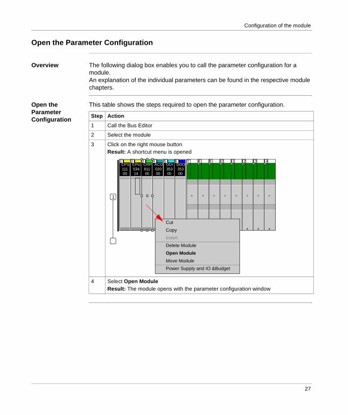
Open the Parameter Configuration
Overview The following dialog box enables you to call the parameter configuration for a module.An explanation of the individual parameters can be found in the respective module chapters.
Open the Parameter Configuration
This table shows the steps required to open the parameter configuration.
Step Action
1 Call the Bus Editor
2 Select the module
3 Click on the right mouse buttonResult: A shortcut menu is opened
4 Select Open ModuleResult: The module opens with the parameter configuration window
1CPS11100
2CPU53414
3CRP81100
4ACO02000
5DDI35300
6DDO35300
7 8 9 10 11 12 13 14
CopyInsertDelete ModuleOpen ModuleMove ModulePower Supply and IO &Budget
Cut
1
27

Configuration of the module
28

2
Quantum Addressing ModesOverview
Purpose This chapter provides information on the three different modes Unity Pro allows to address the I/O data from a Quantum I/O module:
Flat AddressingTopological AddressingIODDT Addressing
While Flat Addressing and Topological Addressing are available for all Quantum I/O modules, IODDTs are only provided for modules which deliver information additional to the I/O values (e.g. errors or warnings).
Also provided is information about the I/O modules status byte and about bit order.
What's in this Chapter?
This chapter contains the following topics:
Note: The different addressing modes refer to the same physical location in the PLC memory for a given data point.
Topic Page
Flat Addressing 30
Topological Addressing 31
IODDT Addressing 32
Quantum IODDTs 33
Addressing Example 35
Discrete I/O Bit Numbering 36
I/O Modules Status Byte 37
I/O Configuration for Discrete Input Modules 40
I/O Configuration for Discrete Output Modules 46
I/O Configuration for Discrete Input/Output Modules 53
29
Addressing
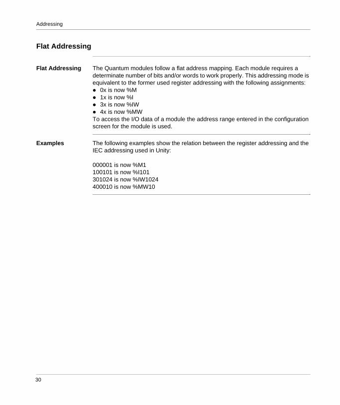
Flat Addressing
Flat Addressing The Quantum modules follow a flat address mapping. Each module requires a determinate number of bits and/or words to work properly. This addressing mode is equivalent to the former used register addressing with the following assignments:
0x is now %M1x is now %I3x is now %IW4x is now %MW
To access the I/O data of a module the address range entered in the configuration screen for the module is used.
Examples The following examples show the relation between the register addressing and the IEC addressing used in Unity: 000001 is now %M1100101 is now %I101301024 is now %IW1024400010 is now %MW10
30
Addressing
Topological Addressing
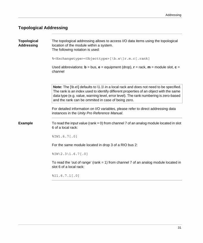
Topological Addressing
The topological addressing allows to access I/O data items using the topological location of the module within a system. The following notation is used:
%<Exchangetype><Objecttype>[\b.e\]r.m.c[.rank]
Used abbreviations: b = bus, e = equipment (drop), r = rack, m = module slot, c = channel
For detailed information on I/O variables, please refer to direct addressing data instances in the Unity Pro Reference Manual.
Example To read the input value (rank = 0) from channel 7 of an analog module located in slot 6 of a local rack:
%IW1.6.7[.0]
For the same module located in drop 3 of a RIO bus 2:
%IW\2.3\1.6.7[.0]
To read the ’out of range’ (rank = 1) from channel 7 of an analog module located in slot 6 of a local rack:
%I1.6.7.1[.0]
Note: The [\b.e\] defaults to \1.1\ in a local rack and does not need to be specified.The rank is an index used to identify different properties of an object with the same data type (e.g. value, warning level, error level). The rank numbering is zero-based and the rank can be ommited in case of being zero.
31

Addressing
IODDT Addressing
IODDT Addressing
An IODDT allows all information (bits and registers) related to a channel to be handled through a user-defined variable. This variable is defined in the Unity Pro data editor by selecting the appropriate IODDT for the module as a data type and specifying the topological address of the module using the following syntax:%CH[\b.e\]r.m.cwhere:
b = buse = equipment (drop)r = rackm = module slotc = channel
Here is an example of an IODDT for an thermocouple input module in slot 4 of a local rack:
Variables in the User Program
You can access all information related to channel 1 of the module using the following variables:
My_Temp_Point1.VALUE for the measured valueMy_Temp_Point1.ERROR indicating an out-of-range conditionMy_Temp_Point1.WARNING indicating an over-range condition
Data Editor
Name Type CommentAddress
Variables DDT Types Function DFB Types
Name *
0 01
FilterEDT
Value
DDT
%CH1.4.1%IW1.4.1.%I1.4.1.1%I1.4.1.2
VALUEERROR
IODDT
My_Temp_Point1 T_ANA_IN_VWEIntBoolBoolWARNING
Channel 1 DataTemperatur ValueOut of RangeRange Warning
Note: Only %CH1.4.1 needs to be entered. The topological addresses re-lated to this channel (%IW.. and %I..) are generated automatically.
32
Addressing
Quantum IODDTs
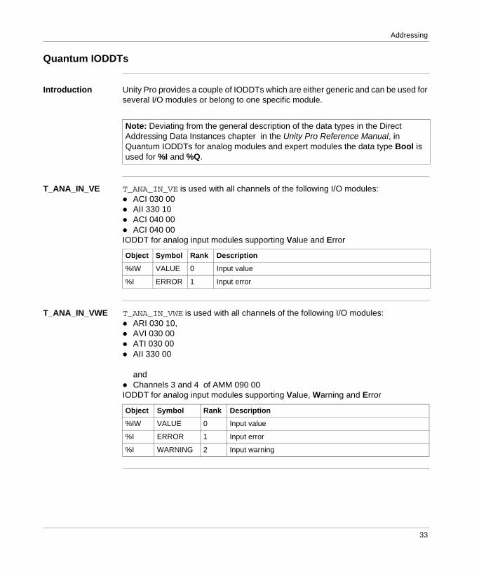
Introduction Unity Pro provides a couple of IODDTs which are either generic and can be used for several I/O modules or belong to one specific module.
T_ANA_IN_VE T_ANA_IN_VE is used with all channels of the following I/O modules:ACI 030 00AII 330 10ACI 040 00ACI 040 00
IODDT for analog input modules supporting Value and Error
T_ANA_IN_VWE T_ANA_IN_VWE is used with all channels of the following I/O modules:ARI 030 10,AVI 030 00ATI 030 00AII 330 00
andChannels 3 and 4 of AMM 090 00
IODDT for analog input modules supporting Value, Warning and Error
Note: Deviating from the general description of the data types in the Direct Addressing Data Instances chapter in the Unity Pro Reference Manual, in Quantum IODDTs for analog modules and expert modules the data type Bool is used for %I and %Q.
Object Symbol Rank Description
%IW VALUE 0 Input value
%I ERROR 1 Input error
Object Symbol Rank Description
%IW VALUE 0 Input value
%I ERROR 1 Input error
%I WARNING 2 Input warning
33

Addressing
T_ANA_BI_VWE T_ANA_BI_VWE is used with the following I/O modules:Channels 1 and 2 of AMM 090 00
IODDT for bidirectional analog modules supporting Value, Warning and Error
T_CNT_105 T_CNT_105 is used with all channels of the following I/O modules:EHC 105
Specific IODDT for high speed counter module EHC 105
Object Symbol Rank Description
%IW VALUE_IN 0 Input value
%QW VALUE_OUT 0 Output value
%I ERROR_IN 1 Input error
%I WARNING 2 Input warning
%I ERROR_OUT 3 Output error
Object Symbol Rank Description
%IW VALUE_L 1 Input value: Low word
%IW VALUE_H 2 Input value: High word
%I ERROR 1 Error in Counter
%I SP_FINAL 2 Final Set Point signal
%I SP_FIRST 3 First Set Point signal
%I SP_SECOND 4 Second Set Point signal
%QW STOP_VALUE 1 For CNT_DIR="0", final set point value
%QW INITIAL_VALUE 2 For CNT_R="1", initial set point value
%Q LS 1 "1", Counter load/start (controlled by the rising edge)
%Q RSTART 2 "1", Counter restart (controlled by the rising edge)
%Q OUT_OFF 3 "1", Counter output switch-off
%Q CNT_DIR 4 "0" Counter counts up"1" Counter counts down
%Q OM1 5 Operating Mode bit 1
%Q OM2 6 Operating Mode bit 2
%Q OM3 7 Operating Mode bit 3
%Q OM4 8 Operating Mode bit 4
34

Addressing
Addressing Example
Example for the 3 Addressing Modes
The following example compares the 3 possible addressing modes. An 8-channel thermocouple 140 ATI 030 00 module with the following configuration data is used:
mounted in slot 5 of the CPU rack (local rack)starting input address is 201 (input word %IW201)end input address is 210 (input word %IW210)
To access the I/O data from the module you can use the following syntax:
For comparison, the register addressing as used with Concept is added in the last column. As Concept does not support direct addressing of a bit in a word, the bit extraction has to be performed in the user program.
Module data Flat addressing
Topological addressing
IODDT addressing Concept addressing
Channel 3temperature
%IW203 %IW1.5.3 My_Temp.VALUE 300203
Channel 3out of range
%IW209.5 %I1.5.3.1 My_Temp.ERROR 300209Bit 5 to be extracted by user-logic
Channel 3range warning
%IW209.13 %I1.5.3.2 My_Temp.WARNING 300209Bit 13 to be extracted by user-logic
Module internal temperature
%IW210 %IW1.5.10 not accessible through IODDT
300210
Note: For the IODDT the data type T_ANA_IN_VWE is used and the variable My_Temp with the address %CH1.5.10 was defined.
35

Addressing
Discrete I/O Bit Numbering
Introduction The numbering of channels of an I/O module usually starts with 1 and counts up to the maximum number of supported channels. The software however starts numbering with a 0 for the least significant bit in a word (LSB). Additional the Quantum I/O modules have their lowest channel mapped to the most significant bit (MSB).The following figure shows the mapping of I/O channels related to the bits in a word:.
Word Addressing versus Bit Addressing
Mainly discrete I/O modules can be configured to deliver their I/O data either in word format or in bit format. This can be selected during configuration by selecting either %IW (%MW) or %I (%M). If you need to access a single bit from an I/O module configured to use an I/O word, you can use the syntax %word.bit. The following table gives you the connection between I/O point number and the belonging I/O address in bit and word addressing. The table shows an 32-point input module in the main rack, slot 4 configured with starting address %I1 or %IW1:
1 2 3 4 5 6 7 10 11 12 13 14 15 168 9
15 14 13 12 11 10 9 6 5 4 3 2 1 08 7
I/O ChannelsBit numbering
MSB LSB
I/O channel
Bit address(flat addressing)
Bit address(topological addressing)
Bit addressextracted from word(flat addressing)
Bit addressextracted from word(topological addressing)
1 %I1 %I1.4.1[.0] %IW1.15 %IW1.4.1.1.15
2 %I2 %I1.4.2[.0] %IW1.14 %IW1.4.1.1.14
3 %I3 %I1.4.3[.0] %IW1.13 %IW1.4.1.1.13
• • •
15 %I15 %I1.4.15[.0] %IW1.1 %IW1.4.1.1.1
16 %I16 %I1.4.16[.0] %IW1.0 %IW1.4.1.1.0
17 %I17 %I1.4.17[.0] %IW2.15 %IW1.4.1.2.15
18 %I18 %I1.4.18[.0] %IW2.14 %IW1.4.1.2.14
• • •
31 %I31 %I1.4.31[.0] %IW2.1 %IW1.4.1.2.1
32 %I32 %I1.4.32[.0] %IW2.0 %IW1.4.1.2.0
36

Addressing
I/O Modules Status Byte
Addressing Module Status Data
In addition to possible channel related diagnostics data, a module related status byte may be used. The status information of all modules in a Drop is administered by a table of %IW words. The starting address of this table can be entered in the configuration screen for the Drop. This information is not accessible through topological addressing.
Example of a Drop configuration screen with the starting address of the status table set to 100:
Note: The status information is only available if the module supports a status byte. For the meaning of the status byte check the module descriptions.
Quantum Drop for local
Quantum Drop for local
BIT (%I-1X)
Overview ConfigParameter Name Value
MAST
115Starting address status tableEnding address statusDrop hold up time 100msIn Bytes
376
100
Local Quant... 1.4: 140 A...
MASTOut Bytes 32
Data Editor... fbtest: (M...0 01 Quantum Dr...FBD
37

Addressing
The following illustration shows how one word of the table conveys the status information for two modules:
Example The following example shows a rack and the corresponding I/O status bytes displayed in an animation table. The drop is configured to start at word %IW100 and allocates 16 words. This represents the local and expansion rack, and assumes they are 16 slot racks.If a module does not have have a status byte associated with the module or the slot is empty, then the byte = 0.
8 7 26 5 4 3 1
Slot 2 Slot 1
I/O Status B I/O Status A
%IW100
%IW102
Slot 4 Slot 3
Slot 6 Slot 5
Slot 1 2 3 4 5 6
%IW101
I/O Status C
I/O
AModule
I/O
BModule
I/O
CModule
8 7 26 5 4 3 1
I/O Status Bits I/O Status Bits
38

Addressing
Rack configuration and Animation table:
Relation between Slot, Input Word and Status Byte. The byte related to the module is marked:
Slot Input Word
Value Module Module
1 %IW[0] 0 Power Supply no Status Byte
2 0 CPU no Status Byte
3 %IW[1] 2#1000_0000_0000_0000 CPU no Status Byte
4 2#1000_0000_0000_0000 AVI At least one channel fault
5 %IW[2] 2#0000_0000_0000_1111 ATI Fault on channels 1 ... 4
6 2#0000_0000_0000_1111 CRP no Status Byte
7 %IW[3] 0 Empty
8 0 Empty
9 %IW[4] 2#0000_0000_0011_1111 DDO Fault on all channels
10 2#0000_0000_0011_1111 XBE no Status Byte
• • •
1CPS21400
2CPU67160
3ACI03000
4AVI03000
5ATI03000
6CRP93X00
7 8 15 16 11 12 13 14
1
2CPU65160
9DDO36400
10XBE10000
Table
Name%IW100:16
Value
0
TypeARRAY[0.. 1..Int
Comment
Modifica- Force
%IW100[0]Int%IW100[1]
2#0000_0000_0000_111 Int%IW100[2]0 Int%IW100[3]2#0000_0000_0011_111 Int0 Int0 Int0 Int
%IW100[4]%IW100[5]%IW100[6]%IW100[7]
0 Int%IW100[8]0 Int%IW100[9]0 Int%IW100[10]0 Int%IW100[11]0 Int0 Int0 Int0 Int
%IW100[12]%IW100[13]%IW100[14]%IW100[15]
2#1000_0000_0000_000
39

Addressing
I/O Configuration for Discrete Input Modules
Overview This section provides information on configuration of 8-, 16-, 24-, 32-, and 96-point input modules.
8-Point Input Modules
The 8-point input modules are:140DII33000 (DC Input Intrinsically Safe)
Flat Addressing The input modules listed above can be configured as either 8 contiguous %I references or as one %IW word. For a description of how to access the input points, please refer to Discrete I/O Bit Numbering, p. 36.
Topological Addressing
The following tables show the topological addresses for the 8-Point Input Modules.Topological addresses in Bit Mapping format:
Topological addresses in Word Mapping format:
Used abbreviations: b = bus, e = equipment (drop), r = rack, m = module slot.
I/O Map Status Byte
There is no I/O map status byte associated with these modules.
2 3 4 5 6 7 8 1
MSB
Point I/O Object Comment
Input 1 %I[\b.e\]r.m.1 Value
Input 2 %I[\b.e\]r.m.2 Value
• • •
Input 7 %I[\b.e\]r.m.7 Value
Input 8 %I[\b.e\]r.m.8 Value
Point I/O Object Comment
Inputword 1 %IW[\b.e\]r.m.1.1 Value
40

Addressing
16-Point Input Modules
The 16-point input modules are:140DAI34000 (AC Input 24 Vac 16x1)140DAI44000 (AC Input 48 Vac 16x1)140DAI54000 (AC Input 115 Vac 16x1)140DAI54300 (AC Input 115 Vac 8x2)140DAI74000 (AC Input 230 Vac 16x1)140DDI84100 (DC Input 10 ... 60 Vdc 8x2 Sink)140HLI34000 (DC Input 24 Vdc 16 Sink/Source)
Flat Addressing The input modules listed above can be configured as either 16 contiguous %I references or as one %IW word. For a description of how to access the input points, please refer to Discrete I/O Bit Numbering, p. 36.
Topological Addressing
The following tables show the topological addresses for the 16-Point Input Modules.Topological addresses in Bit Mapping format:
Topological addresses in Word Mapping format:
Used abbreviations: b = bus, e = equipment (drop), r = rack, m = module slot.
I/O Map Status Byte
There is no I/O map status byte associated with these modules.
24-Point Input Module
There is only one 24-point input module: 140DDI67300 (DC Input 125 VDC 3x8 Sink)
1 2 3 4 5 6 7 10 11 12 13 14 15 168 9
MSB
Point I/O Object Comment
Input 1 %I[\b.e\]r.m.1 Value
Input 2 %I[\b.e\]r.m.2 Value
• • •
Input 15 %I[\b.e\]r.m.15 Value
Input 16 %I[\b.e\]r.m.16 Value
Point I/O Object Comment
Inputword 1 %IW[\b.e\]r.m.1.1 Value
41

Addressing
Flat Addressing The input module listed above can be configured as either 24 contiguous discrete input %I reference, or as 2 contiguous %IW input words in the following format. For a description of how to access the input points, please refer to Discrete I/O Bit Numbering, p. 36.
Topological Addressing
The following tables show the topological addresses for the 24-Point Input Modules.Topological addresses in Bit Mapping format:
Topological addresses in Word Mapping format:
Used abbreviations: b = bus, e = equipment (drop), r = rack, m = module slot.
I/O Map Status Byte
There is no input I/O map status byte associated with this module.
1 2 3 4 5 6 7 10 11 12 13 14 15 168 9
18 19 20 21 22 23 2417
MSB - First WordInputPoint 1
MSB - Second WordInputPoint 17
Point I/O Object Comment
Input 1 %I[\b.e\]r.m.1 Value
Input 2 %I[\b.e\]r.m.2 Value
• • •
Input 23 %I[\b.e\]r.m.23 Value
Input 24 %I[\b.e\]r.m.24 Value
Point I/O Object Comment
Inputword 1 %IW[\b.e\]r.m.1.1 Value
Inputword 2 %IW[\b.e\]r.m.1.2 Value
42

Addressing
32-Point Input Modules
The 32-point input modules are as follows:140DAI35300 (AC Input 24 Vac 4x8)140DAI45300 (AC Input 48 Vac 4x8)140DAI55300 (AC Input 115 Vac 4x8)140DAI75300 (AC Input 230 Vac 4x8)140DDI15310 (DC Input 5 V TTL 4x8 Source)140DDI35300 (DC Input 24 Vdc 4x8 Sink)140DDI35310 (DC Input 24 Vdc 4x8 Source)140DDI85300 (DC Input 10 ... 60 Vdc 4x8 Sink)
For addressing information of the 140DSI353000, please refer to Addressing, p. 303.
Flat Addressing The input modules listed above can be configured as either 32 contiguous discrete input %I references or as two contiguous %IW input words in the following format. For a description of how to access the input points, please refer to Discrete I/O Bit Numbering, p. 36.
Topological Addressing
The following tables show the topological addresses for the 32-Point Input Modules.Topological addresses in Bit Mapping format:
Topological addresses in Word Mapping format:
Used abbreviations: b = bus, e = equipment (drop), r = rack, m = module slot.
1 2 3 4 5 6 7 10 11 12 13 14 15 168 9
17 18 19 20 21 22 23 26 27 28 29 30 31 3224 25
MSB - First WordInputPoint 1
MSB - Second WordInputPoint 17
Point I/O Object Comment
Input 1 %I[\b.e\]r.m.1 Value
Input 2 %I[\b.e\]r.m.2 Value
• • •
Input 31 %I[\b.e\]r.m.31 Value
Input 32 %I[\b.e\]r.m.32 Value
Point I/O Object Comment
Inputword 1 %IW[\b.e\]r.m.1.1 Value
Inputword 2 %IW[\b.e\]r.m.1.2 Value
43
Addressing
I/O Map Status Byte
There is no I/O map status byte associated with these modules.
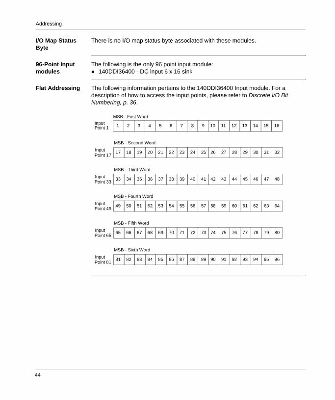
96-Point Input modules
The following is the only 96 point input module:140DDI36400 - DC input 6 x 16 sink
Flat Addressing The following information pertains to the 140DDI36400 Input module. For a description of how to access the input points, please refer to Discrete I/O Bit Numbering, p. 36.
1 2 3 4 5 6 7 10 11 12 13 14 15 168 9
17 18 19 20 21 22 23 26 27 28 29 30 31 3224 25
MSB - First WordInputPoint 1
MSB - Second WordInputPoint 17
33 34 35 36 37 38 39 42 43 44 45 46 47 4840 41
MSB - Third WordInputPoint 33
49 50 51 52 53 54 55 58 59 60 61 62 63 6456 57
MSB - Fourth WordInputPoint 49
65 66 67 68 69 70 71 74 75 76 77 78 79 8072 73
MSB - Fifth WordInputPoint 65
81 82 83 84 85 86 87 90 91 92 93 94 95 9688 89
MSB - Sixth WordInputPoint 81
44

Addressing
Topological Addressing
The following tables show the topological addresses for the 96-Point Input Modules.Topological addresses in Bit Mapping format:
Topological addresses in Word Mapping format:
Used abbreviations: b = bus, e = equipment (drop), r = rack, m = module slot.
I/O Map Status Byte
There is no I/O map status byte associated with this module.
Point I/O Object Comment
Input 1 %I[\b.e\]r.m.1 Value
Input 2 %I[\b.e\]r.m.2 Value
• • •
Input 95 %I[\b.e\]r.m.95 Value
Input 96 %I[\b.e\]r.m.96 Value
Point I/O Object Comment
Inputword 1 %IW[\b.e\]r.m.1.1 Value
Inputword 2 %IW[\b.e\]r.m.1.2 Value
Inputword 3 %IW[\b.e\]r.m.1.3 Value
Inputword 4 %IW[\b.e\]r.m.1.4 Value
Inputword 5 %IW[\b.e\]r.m.1.5 Value
Inputword 6 %IW[\b.e\]r.m.1.6 Value
45

Addressing
I/O Configuration for Discrete Output Modules
Overview This section provides information on configuration of 8-, 12-, 16-, 32- and 96-point output modules.
8-Point Output Modules
The following shows the 8-point output module:140DRC83000 (Relay Ouput 8x1 Normally Open/Normally Closed)
Flat Addressing The ouput modules listed above can be configured as either eight contiguous discrete %M output references or as one %MW output word. For a description of how to access the input points, please refer to Discrete I/O Bit Numbering, p. 36.
Topological Addressing
The following tables show the topological addresses for the 8-Point Output Modules.Topological addresses in Bit Mapping format:
Topological addresses in Word Mapping format:
Used abbreviations: b = bus, e = equipment (drop), r = rack, m = module slot.
I/O Map Status Byte
There is no I/O Map status byte associated with these modules.
12-Point Output Module
The 12-point output module is:140DDO88500
2 3 4 5 6 7 81
MSB
Point I/O Object Comment
Output 1 %Q[\b.e\]r.m.1 Value
Output 2 %Q[\b.e\]r.m.2 Value
• • •
Output 7 %Q[\b.e\]r.m.7 Value
Output 8 %Q[\b.e\]r.m.8 Value
Point I/O Object Comment
Outputword 1 %QW[\b.e\]R.S.1.1 Value
46

Addressing
Flat Addressing (Fault Inputs)
The Fault Inputs of the 140DDO88500 can be configured as either 16 contiguous %I references or as one %IW word. For a description of how to access the input points, please refer to Discrete I/O Bit Numbering, p. 36.
Topological Addressing
The following tables show the topological addresses for the 12-Point Fault Inputs.Topological addresses in Bit Mapping format:
Topological addresses in Word Mapping format:
Used abbreviations: b = bus, e = equipment (drop), r = rack, m = module slot.
Flat Addressing (Outputs)
The 140DDO88500 can be configured as one %MW output word in the following format. For a description of how to access the input points, please refer to Discrete I/O Bit Numbering, p. 36.
1 2 3 4 5 6 7 10 11 128 9
MSB
Point I/O Object Comment
Input 1 %I[\b.e\]r.m.1 Value
Input 2 %I[\b.e\]r.m.2 Value
• • •
Input 11 %I[\b.e\]r.m.11 Value
Input 12 %I[\b.e\]r.m.12 Value
Point I/O Object Comment
Inputword 1 %IW[\b.e\]r.m.1.1 Value
1 2 3 4 5 6 7 10 11 128 9
MSB
47

Addressing
Topological Addressing
The following tables show the topological addresses for the 12-Point Output Modules.Topological addresses in Bit Mapping format:
Topological addresses in Word Mapping format:
Used abbreviations: b = bus, e = equipment (drop), r = rack, m = module slot.
I/O Map Status Byte (Outputs)
The least significant bit in the output I/O map status byte is used as follows. For a description of how to access the input points, please refer to Discrete I/O Bit Numbering, p. 36.
16-Point Output Modules
The 16-point output modules are as follows:140DAO84000 (AC Output 24 ... 230 Vac 16x1)140DAO84010 (AC Output 24 ... 115 Vac 16x1)140DAO84210 (AC Output 100 ... 230 Vac 4x4)140DAO84220 (AC Output 48 Vac 4x4)140DDO84300 (DC Output 10 ... 60 VDC 2x8 Source)140DRA84000 (Relay Output 16x1 Normally Open)
Point I/O Object Comment
Output 1 %Q[\b.e\]r.m.1 Value
Output 2 %Q[\b.e\]r.m.2 Value
• • •
Output 11 %Q[\b.e\]r.m.11 Value
Output 12 %Q[\b.e\]r.m.12 Value
Point I/O Object Comment
Outputword 1 %QW[\b.e\]r.m.1.1 Value
Module Fault(any point fault turns on this bit)
12345678
MSB
48

Addressing
Flat Addressing The output modules listed above can be configured as either 16 contiguous discrete %M output references, or as one %MW output word in the following formats. For a description of how to access the input points, please refer to Discrete I/O Bit Numbering, p. 36.
Topological Addressing
The following tables show the topological addresses for the 16-Point Output Modules.Topological addresses in Bit Mapping format:
Topological addresses in Word Mapping format:
Used abbreviations: b = bus, e = equipment (drop), r = rack, m = module slot.
I/O Map Status Byte
The I/O map status byte is used by the 140DAO84210 and 140DAO84220 output modules. The following figure shows I/O map status bytes use.
There is no I/O map status byte associated with the 140DAO84000, 140DAO84010, 140DDO84300, or 140DRA84000 module.
1 2 3 4 5 6 7 10 11 12 13 14 15 168 9
MSB
Point I/O Object Comment
Output 1 %Q[\b.e\]r.m.1 Value
Output 2 %Q[\b.e\]r.m.2 Value
• • •
Output 15 %Q[\b.e\]r.m.15 Value
Output 16 %Q[\b.e\]r.m.16 Value
Point I/O Object Comment
Outputword 1 %QW[\b.e\]r.m.1.1 Value
12345678
Group D fault
Group C fault Group B fault
Group A fault
49

Addressing
32-Point Output Modules
The following list shows the 32-point output modules:140DAO85300 (AC Output 230 Vac 4x8 Sink)140DDO15310 (DC Output 5 V TTL 4x8 Sink)140DDO35300 (DC Output 24 Vdc 4x8 Source)140DDO35301 (DC Output 24 Vdc 4x8 Source)140DDO35310 (DC Output 24 Vdc True Low 4x8 Sink)
For addressing information of the 140DVO85300, please refer to Addressing, p. 454.
Flat Addressing The output modules listed above can be configured as either 32 contiguous %M references, or as two %MW words in the following format. For a description of how to access the input points, please refer to Discrete I/O Bit Numbering, p. 36.
Topological Addressing
The following tables show the topological addresses for the 32-Point Output Modules.Topological addresses in Bit Mapping format:
Topological addresses in Word Mapping format:
Used abbreviations: b = bus, e = equipment (drop), r = rack, m = module slot.
1 2 3 4 5 6 7 10 11 12 13 14 15 168 9
17 18 19 20 21 22 23 26 27 28 29 30 31 3224 25
Output Point 1
MSB - Second Word
MSB - First Word
OutputPoint 17
Point I/O Object Comment
Output 1 %Q[\b.e\]r.m.1 Value
Output 2 %Q[\b.e\]r.m.2 Value
• • •
Output 31 %Q[\b.e\]r.m.31 Value
Output 32 %Q[\b.e\]r.m.32 Value
Point I/O Object Comment
Outputword 1 %QW[\b.e\]r.m.1.1 Value
Outputword 2 %QW[\b.e\]r.m.1.2 Value
50

Addressing
I/O Map Status Byte
The I/O map status byte is used by the modules as follows:
96-Point Output Module
The 96 point output module is:140DDO36400 - DC out 24VDC 6x16 Source
Flat Addressing The following figures show the words 1 through 6 format for the 140DDO36400 output module. For a description of how to access the input points, please refer to Discrete I/O Bit Numbering, p. 36.
Groupt A Fault
12345678
Group B FaultGroup C Fault
Group D FaultGroup A Point Fault
Group B Point FaultGroup C Point Fault
Group D Point Fault
140DDO35301 Module only(overload or short circuit)
Missing field poweror blown fues
1 2 3 4 5 6 7 10 11 12 13 14 15 168 9
17 18 19 20 21 22 23 26 27 28 29 30 31 3224 25
MSB - First WordOutputPoint 1
MSB - Second WordOutputPoint 17
33 34 35 36 37 38 39 42 43 44 45 46 47 4840 41
MSB - Third WordOutputPoint 33
49 50 51 52 53 54 55 58 59 60 61 62 63 6456 57
MSB - Fourth WordOutputPoint 49
65 66 67 68 69 70 71 74 75 76 77 78 79 8072 73
MSB - Fifth WordOutputPoint 65
81 82 83 84 85 86 87 90 91 92 93 94 95 9688 89
MSB - Sixth WordOutputPoint 81
51

Addressing
Topological Addressing
The following tables show the topological addresses for the 16-Point Output Modules.Topological addresses in Bit Mapping format:
Topological addresses in Word Mapping format:
Used abbreviations: b = bus, e = equipment (drop), r = rack, m = module slot.
I/O Map Status Byte
The I/O map status byte is used by the module as follows:
Point I/O Object Comment
Output 1 %Q[\b.e\]r.m.1 Value
Output 2 %Q[\b.e\]r.m.2 Value
• • •
Output 95 %Q[\b.e\]r.m.95 Value
Output 96 %Q[\b.e\]r.m.96 Value
Point I/O Object Comment
Outputword 1 %QW[\b.e\]r.m.1.1 Value
Outputword 2 %QW[\b.e\]r.m.1.2 Value
Outputword 3 %QW[\b.e\]r.m.1.3 Value
Outputword 4 %QW[\b.e\]r.m.1.4 Value
Outputword 5 %QW[\b.e\]r.m.1.5 Value
Outputword 6 %QW[\b.e\]r.m.1.6 Value
Output 1 to 16 Fault
12345678
Output 17 to 32 FaultOutput 33 to 48 Fault
Output 49 to 64 FaultOutput 65 to 80 Fault
Output 80 to 96 Fault
52

Addressing
I/O Configuration for Discrete Input/Output Modules
Overview This section provides information on configuration of 4 In/4 Out and 16 In/8 Out modules.
4-Point Input/4-Point Output Module
The following shows the 4 In/4 Out module:140DDM69000 (125 Vdc Input/High Power Output)
Flat Addressing The 140DDM69000 input/output module can be configured as either eight contiguous %I references; or as one %IW word and either eight contiguous %M references or one %MW word.
I/O Map Register (Inputs)
The following figure shows the %IW input word.
CAUTIONI/O MappingWhen I/O mapping module inputs using discrete %I references in remote drops, users should not split discrete words between drops. The lowest discrete reference for a drop should start on a word boundary.Failure to follow this precaution can result in injury or equipment damage.
Output 1 Fault
Input 1
2 3 4 5 6 7 81
Input 2Input 3
Input 4
Output 2 FaultOutput 3 Fault
Output 4 Fault
53
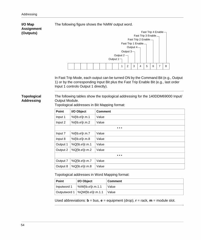
Addressing
I/O Map Assignment (Outputs)
The following figure shows the %MW output word.
In Fast Trip Mode, each output can be turned ON by the Command Bit (e.g., Output 1) or by the corresponding Input Bit plus the Fast Trip Enable Bit (e.g., last order Input 1 controls Output 1 directly).
Topological Addressing
The following tables show the topological addressing for the 140DDM69000 Input/Output Module.Topological addresses in Bit Mapping format:
Topological addresses in Word Mapping format:
Used abbreviations: b = bus, e = equipment (drop), r = rack, m = module slot.
Fast Trip 1 Enable
Output 1
2 3 4 5 6 7 81
Output 2Output 3
Output 4
Fast Trip 2 EnableFast Trip 3 Enable
Fast Trip 4 Enable
Point I/O Object Comment
Input 1 %I[\b.e\]r.m.1 Value
Input 2 %I[\b.e\]r.m.2 Value
• • •
Input 7 %I[\b.e\]r.m.7 Value
Input 8 %I[\b.e\]r.m.8 Value
Output 1 %Q[\b.e\]r.m.1 Value
Output 2 %Q[\b.e\]r.m.2 Value
• • •
Output 7 %Q[\b.e\]r.m.7 Value
Output 8 %Q[\b.e\]r.m.8 Value
Point I/O Object Comment
Inputword 1 %IW[\b.e\]r.m.1.1 Value
Outputword 1 %QW[\b.e\]r.m.1.1 Value
54

Addressing
I/O Map Status Byte (Outputs)
The four least significant bits in the I/O map status are used as follows:
16-Point Input/8-Point Output Modules
The following information pertains to the 140DAM59000 (AC Input 115 Vac 2x8 / AC Output 115 Vac 2x4) and the 140DDM39000 (DC Input 24 Vdc 2x8 / DC Output 24 Vdc 2x4) modules.
140DAM59000 (AC Input 115 Vac 2x8 / AC Output 115 Vac 2x4)140DDM3900 (DC Input 24 Vdc 2X8 / DC Output 24 Vdc 2x4)
Flat Addressing The modules listed above can be configured as either 16 contiguous %I references or as one %IW word and as one %MW word.
I/O Map Register (Inputs)
The following figure shows the %IW input word. For a description of how to access the input points, please refer to Discrete I/O Bit Numbering, p. 36.
I/O Map Assignment (Outputs)
The modules listed above can be configured as 8 %M references or as 1 %MW output word in the following format. For a description of how to access the input points, please refer to Discrete I/O Bit Numbering, p. 36.
Output 1 Fault
12345678
Output 2 FaultOutput 3 Fault
Output 4 Fault
1 2 3 4 5 6 7 10 11 12 13 14 15 168 9
MSB
1 2 3 4 5 6 7 8
MSB
55

Addressing
Topological Addressing
The following tables show the topological addresses for the 16/8-Point Input/Output Modules.Topological addresses in Bit Mapping format:
Topological addresses in Word Mapping format:
Used abbreviations: b = bus, e = equipment (drop), r = rack, m = module slot.
I/O Map Status Byte (Outputs)
The two least significant bits in the output I/O map status byte are used as follows.
Point I/O Object Comment
Input 1 %I[\b.e\]r.m.1 Value
Input 2 %I[\b.e\]r.m.2 Value
• • •
Input 15 %I[\b.e\]r.m.15 Value
Input 16 %I[\b.e\]r.m.16 Value
Output 1 %Q[\b.e\]r.m.1 Value
Output 2 %Q[\b.e\]r.m.2 Value
• • •
Output 7 %Q[\b.e\]r.m.7 Value
Output 8 %Q[\b.e\]r.m.8 Value
Point I/O Object Comment
Inputword 1 %IW[\b.e\]r.m.1.1 Value
Outputword 1 %QW[\b.e\]r.m.1.1 Value
12345678
Group B fault
Group A fault
56

II
Analog IN ModulesAt a Glance
Introduction The following part provides information on the Quantum Analog IN modules.
What's in this Part?
This part contains the following chapters:
Chapter Chapter Name Page
3 140 ACI 030 00: Analog Current / Voltage IN Module 59
4 140 ACI 040 00: Analog Mixed Current IN Module 69
5 140 ARI 030 10: Analog RTD IN Module 79
6 140 ATI 030 00: Analog TC IN Module 91
7 140 AVI 030 00: Analog Mixed Current/Voltage IN Module 103
57

Analog IN Modules
58

3
140 ACI 030 00: Analog Current / Voltage IN ModuleOverview
Purpose The following chapter provides information of the Quantum 140 ACI 030 00 Module.
What's in this Chapter?
This chapter contains the following topics:
Topic Page
Presentation 60
Indicators 61
Wiring Diagram 62
Specifications 64
Addressing 66
Parameter Configuration 68
59

140 ACI 030 00
Presentation
Function The Analog Input 8 Channel Unipolar module accepts mixed current and voltage inputs. Required jumpers between the input and sense terminals for current input measuring are included with the module.
Illustration The following figure shows the140 ACI 030 00 module and its components.
1 Model Number, Module Description, Color Code
2 LED Display
3 Fuse Cutouts
4 Field Wiring Terminal Strip
5 Removable Door
6 Customer Identification Label (Fold label and place it inside door)
Note: The field wiring terminal strip (Modicon #140 XTS 002 00) must be ordered separately. (The terminal strip includes the removable door and label.)
140ACI 030 00
X X
XXXXXXXXXXXXXXXXXXXX
XXXXXXXXXXXXXXXXXXXXX
23
6
8
10
1214
16
18
20
21
232527
29
31
3335
37
1
4
7
9
11
13
1517
19
22
24
26
28
30
32
34
3638
1
2
3
4 5
6
60

140 ACI 030 00
Indicators
Illustration The following table shows the LED indicators for the 140 ACI 030 00 module.
Descriptions The following table shows the LED descriptions for the 140 ACI 030 00 module.
Active F
123
4
567
8
LEDs Color Indication when ON
Active Green Bus communication is present.
F Red A fault (external to the module) has been detected.
1 ... 8 Green The indicated point or channel is turned ON.
1 ... 8 Red There is a fault on the indicated point or channel.
Note: This module produces a fault signal F if any one channel detects a broken wire condition in the 4 ... 20 mA range or under voltage (1 ... 5 V only).
61

140 ACI 030 00
Wiring Diagram
Illustration The following figure shows the wiring diagram for the 140 ACI 030 module.
2
10
4
6
8
12
14
16
18
20
22
24
26
28
30
32
34
36
38
40 39
37
35
33
31
29
27
25
23
21
19
17
15
13
11
9
7
5
3
1
N/CINPUT 2(-)
INPUT 1(-)
N/C
N/CINPUT 3(-)
N/CINPUT 4(-)
N/C
N/C
INPUT 5(-)
N/C
INPUT 6(-)
N/C
N/CINPUT 7(-)
N/CINPUT 8(-)
N/C
N/C N/C
I SENSE 8
INPUT 8(+)
I SENSE 7
INPUT 7(+)N/C
I SENSE 6
INPUT
I SENSE 5
INPUT 5(+)
N/C
I SENSE 4
INPUT
I SENSE 3
INPUT 3(+)
N/C
I SENSE 2
INPUT
INPUT 1(+)
I SENSE 1Jumper
Voltage Source
Current Source
-+
-+
62

140 ACI 030 00
Notes on Wiring Diagram
The current and voltage sources are supplied by the user (fusing is at the discretion of the user)Either a shielded or unshielded signal cable may be used. Shielded types should have a shield tied to earth ground near the signal source end.Unused inputs may cause the activation of the F LED. To avoid this occurrence, wire unused channels in voltage mode to a channel that is in use.N / C = Not Connected.
Note: When field wiring the I/O module, the maximum wire size that should be used is 1-14 AWG or 2-16 AWG; the minimum size is 20 AWG.
63

140 ACI 030 00
Specifications
General Specifications
General Specifications
Voltage / Input Voltage / Input
Current / Input Current / Input
Resolution / Conversion
Resolution / Conversion
Module Type 8 Channel IN Differential
External Power Not required
Bus Current required (Module) 240 mA
Power Dissipation 2 W
I/O map 9 input words
Fault Detection Broken wire (4 ... 20 mA mode) or under voltage range (1 ... 5 V)
Operating Voltage (Channel to Channel) 30 VDC (max.)
Absolute Voltage (max.) 50 VDC
Linear Mesuring Range 1 ... 5 VDC
Input Impedance > 20 Mohms
Absolute Current (max.) 25 mA
Linear Measuring Range 4 ... 20 mA
Input Impedance 250 ohms + 0.003%
Resolution 12 bit
Absolute Accuracy Error @ 25 degrees C (voltage mode)
Typical: +/- 0.05% of full scaleMaximum: +/- 0.1% of full scale
Linearity +/- 0.04%
Accuracy drift with temperature Typical: +/- 0.0025% of full scale / degrees CMaximum: +/- 0.005% of full scale / degrees C
Common Mode Rejection -72 dB @ 60 Hz
Input Filter Single pole low pass, -3 dB cutoff @ 15 Hz, +/- 20%
Update Time 5 ms for all channels
64

140 ACI 030 00
Isolation Isolation
Channel to Bus 1000 VDC 3000 Vpp for 1 minute
Note: Calibration is not required for this module.
65

140 ACI 030 00
Addressing
Flat Addressing This module requires nine contiguous, 16-bit words-eight for input data and one for channel status. The data words formats are as follows.
The following shows the word 9 register.
Topological Addressing
Topological addresses for the 140ACI03000 Input Module:
Channel 1 data Word 1
Word 8 Channel 8 data
1 2 3 4 5 6 7 10 11 12 13 14 15 168 9
1 = Broken wire or under voltage on channel 81 = Broken wire or under voltage on channel 7
1 = Broken wire or under voltage on channel 61 = Broken wire or under voltage on channel 5
1 = Broken wire or under voltage on channel 41 = Broken wire or under voltage on channel 3
1 = Broken wire or under voltage on channel 2
1 = Broken wire or under voltage on channel 1
Point I/O Object Comment
Input 1 %IW[\b.e\]r.m.1 Value
%I[\b.e\]r.m.1.1 Broken wire or under voltage
• • •
Input 8 %IW[\b.e\]r.m.8 Value
%I[\b.e\]r.m.8.1 Broken wire or under voltage
Status Word %IW[\b.e\]r.m.9 Status of input channels
66
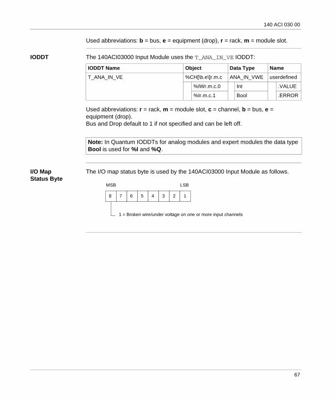
140 ACI 030 00
Used abbreviations: b = bus, e = equipment (drop), r = rack, m = module slot.
IODDT The 140ACI03000 Input Module uses the T_ANA_IN_VE IODDT:
Used abbreviations: r = rack, m = module slot, c = channel, b = bus, e = equipment (drop).Bus and Drop default to 1 if not specified and can be left off.
I/O Map Status Byte
The I/O map status byte is used by the 140ACI03000 Input Module as follows.
IODDT Name Object Data Type Name
T_ANA_IN_VE %CH[\b.e\]r.m.c ANA_IN_VWE userdefined
%IWr.m.c.0 Int .VALUE
%Ir.m.c.1 Bool .ERROR
Note: In Quantum IODDTs for analog modules and expert modules the data type Bool is used for %I and %Q.
12345678
MSB LSB
1 = Broken wire/under voltage on one or more input channels
67

140 ACI 030 00
Parameter Configuration
Parameter and Default values
Parameter Configuration Window
Name Default Value Options Description
Mapping WORD (%IW-3X) -
Inputs Starting Address 1 -
Inputs Ending Address 9 - includes a Statusword
Task(Grayed if module in other than local)
MAST FASTAUX0AUX1AUX2AUX3
fixed to MAST if module in other than local
AN IN 8 CH UNIPOLAR
ConfigParameter Name Value
MAPPING WORD (%IW-3X)INPUTS STARTING ADDRESS 1INPUTS ENDING ADDRESS 9TASK MAST
1 : Local Qu... 2 : 140 ACI.
68

4
140 ACI 040 00: Analog Mixed Current IN ModuleOverview
Purpose The following chapter provides information of the Quantum 140 ACI 040 00 Module.
What's in this Chapter?
This chapter contains the following topics:
Topic Page
Presentation 70
Indicators 71
Wiring Diagram 72
Specifications 74
Addressing 76
Parameter Configuration 78
69

140 ACI 040 00
Presentation
Function The 140 ACI 040 00 is a 16 channel analog input module which accepts mixed current inputs.
Illustration The following figure shows the140 ACI 040 00 module and its components.
1 Model Number, Module Description, Color Code
2 LED Display
3 Fuse Cutouts
4 Field Wiring Terminal Strip
5 Removable Door
6 Customer Identification Label (Fold label and place it inside door)
Note: The field wiring terminal strip (Modicon #140 XTS 002 00) must be ordered separately. (The terminal strip includes the removable door and label.)
140ACI 040 00
X X
XXXXXXXXXXXXXXXXXXXX
XXXXXXXXXXXXXXXXXXXXX
23
6
8
10
1214
16
18
20
21
232527
29
31
3335
37
1
4
7
9
11
13
1517
19
22
24
26
28
30
32
34
3638
1
2
3
4 5
6
70

140 ACI 040 00
Indicators
Illustration The following table shows the LED indicators for the 140 ACI 040 00 module.
Descriptions The following table shows the LED descriptions for the 140 ACI 040 00 module.
Active F
91102113
1245678
13141516
123
45678
91011
1213141516
LEDs Color Indication when ON
Active Green Bus communication is present.
F Red A fault (external to the module) has been detected.
1 ... 16 Green The indicated point or channel is turned ON.
1 ... 16 Red There is a fault on the indicated point or channel.
Note: This module produces a fault signal F if any one channel detects a broken wire condition in the 4 ... 20 mA range
71

140 ACI 040 00
Wiring Diagram
Illustration Wiring diagram for the 140 ACI 040 00 Module.
INPUT13 (-)
INPUT 11 (-)
INPUT 9 (-)
INPUT 7(-)
INPUT 5(-)
2
10
4
6
8
12
14
16
18
20
22
24
26
28
30
32
34
36
38
40 39
37
35
33
31
29
27
25
23
21
19
17
15
13
11
9
7
5
3
1
INPUT 2 (-)
INPUT 3(-)
INPUT 1(-)
INPUT 4 (-)
NC
INPUT 6 (-)
INPUT 8 (-)
N/C
INPUT 10 (-)
INPUT 12 (-)
N/C
INPUT 14 (-)
INPUT 15 (-)
INPUT 16 (-)
N/C N/C
INPUT 16 (+)
INPUT 15(+)
INPUT 14 (+)
INPUT 13(+)
N/C
INPUT 12 (+)
INPUT 11(+)
INPUT 10 (+)
INPUT 9(+)
N/C
INPUT 8 (+)
INPUT 7(+)
INPUT 6 (+)
INPUT 5(+)
N/C
INPUT 4 (+)
INPUT 1(+)-+
-+
INPUT 2(+)
INPUT 3(+)
Current Source
Current Source
DifferentialInput
Single EndedInput
72

140 ACI 040 00
Notes on Wiring Diagram
The current sources are supplied by the user ( fusing is at the discretion of the user.)Either shielded or unshielded cables may be used. In noisy environments twisted shielded cable is recommended. Shielded cable should have a shield tied to earth ground near the signal source end.Unused inputs may cause the activation of the F LED. To avoid this occurrence the unused channels should be configured in the 0 ... 25 mA range.The maximum channel to channel working voltage cannot exceed 30 VDC.N/C = Not connectedWhen field wiring the I/O module, the maximum wire size that should be used is 1-14 AWG or 2-16 AWG; the minimum size is 20 AWG.
73

140 ACI 040 00
Specifications
General Specifications
General Specifications
Current / Input Current / Input
Resolution / Conversion
Resolution / Conversion
Module Type 16 Channel IN (Differential or externally tied single ended)
External Power Not required
Operating Voltage (Channel to Channel)
30 VDC (max.)
Bus Current required (Module) 360 mA
Power Dissipation 5 W
I/O map 17 input words
Fault Detection Broken wire (4 ... 20 mA mode)
Isolation (Field to Bus) 1780 VAC for 1 minute
Absolute Current (max.) 30 mA
Linear Measuring Range 0 ... 25 mA, 0 ... 25,000 counts0 ... 20 mA, 0 ... 20,000 counts4 ... 20 mA, 0 ...16,000 counts4 ... 20 mA, 0 ... 4,095 counts
Input Impedance 250 ohms nominal
Resolution 0 ... 25,000 counts0 ... 20,000 counts0 ...16,000 counts0 ... 4,095 counts
Absolute Accuracy Error @ 25 degrees C +/- 0.125% of full scale
Linearity (0 to 60 degrees C) +/- 12 microA max., 4 ... 20 mA+/- 6 microA max., 0 ... 25 mA+/- 6 microA max., 0 ... 20 mA+/- 6 microA max., 4 ... 20 mA
Accuracy drift with temperature Typical: +/- 0.0025% of full scale / degrees CMaximum: +/- 0.005% of full scale / degrees C
Common Mode Rejection -90 dB @ 60 Hz
Input Filter Single pole low pass, -3 dB cutoff @ 34 Hz, +/- 25%
Update Time 15 ms for all channels
74

140 ACI 040 00
Fuses Fuses
Internal None
External User discretion
75

140 ACI 040 00
Addressing
Flat Addressing This module requires 17 contiguous, 16-bit words—16 for input data and one for channel status. The data words formats are as follows.
The following shows the word 17.
Channel 1 data Word 1
Word 16 Channel 16 data
Input status wordWord 17
1 = Broken wire on channel 13 1 = Broken wire on channel 14
1 = Broken wire on channel 15 1 = Broken wire on channel 16
1 2 3 4 5 6 7 10 11 12 13 14 15 168 9
1 = Broken wire on channel 8*1 = Broken wire on channel 7*
1 = Broken wire on channel 6*1 = Broken wire on channel 5*
1 = Broken wire on channel 9 1 = Broken wire on channel 10
1 = Broken wire on channel 11 1 = Broken wire on channel 12
1 = Broken wire on channel 4*1 = Broken wire on channel 3*
1 = Broken wire on channel 2*
1 = Broken wire on channel 1*
76

140 ACI 040 00
Topological Addressing
Topological addresses for the 140ACI04000 Input Module:
Used abbreviations: b = bus, e = equipment (drop), r = rack, m = module slot.
IODDT The 140ACI04000 Input Module uses the T_ANA_IN_VE IODDT:
Used abbreviations: r = rack, m = module slot, c = channel, b = bus, e = equipment (drop).Bus and Drop default to 1 if not specified and can be left off.
I/O Map Status Byte
The I/O map status byte is used by the 140ACI04000 Input Module as follows.
Point I/O Object Comment
Input 1 %IW[\b.e\]r.m.1 Value
%I[\b.e\]r.m.1.1 Broken wire or under voltage
• • •
Input 16 %IW[\b.e\]r.m.16 Value
%I[\b.e\]r.m.16.1 Broken wire or under voltage
Status Word %IW[\b.e\]r.m.17 Status of input channels
IODDT Name Object Data Type Name
T_ANA_IN_VE %CH[\b.e\]r.m.c ANA_IN_VWE userdefined
%IWr.m.c.0 Int .VALUE
%Ir.m.c.1 Bool .ERROR
Note: In Quantum IODDTs for analog modules and expert modules the data type Bool is used for %I and %Q.
12345678
MSB LSB
1 = Broken wire
77

140 ACI 040 00
Parameter Configuration
Parameter and Default values
Parameter Configuration Window
Name Default Value Options Description
Mapping WORD (%IW-3X) -
Inputs Starting Address 1 -
Inputs Ending Address 17 -
Task(Grayed if module in other than local)
MAST FASTAUX0AUX1AUX2AUX3
fixed to MAST if module in other than local
Channels
Channel1-Channel16 "4 ... 20 mA, 0-16000"
"4 ... 20 mA, 0-4095""0 ... 20 mA, 0-20000"0 ... 25 mA, 0-25000
AN IN 16CH CURR
ConfigParameter Name Value
MAPPING WORD (%IW-3x)1
AUTOMATIC RESTART
1 : Local Qu... 2 : 140 ACI.
CHANNELSCHANNEL1
TASK MAST
INPUTS STARTING ADDRESSINPUTS ENDING ADDRESS 17
“4 ... 20 mA, 0-16000”
CHANNEL3CHANNEL4CHANNEL5
“4 ... 20 mA, 0-16000”“4 ... 20 mA, 0-16000”“4 ... 20 mA, 0-16000”
CHANNEL6 “4 ... 20 mA, 0-16000”
“4 ... 20 mA, 0-16000”CHANNEL2
CHANNEL7 “4 ... 20 mA, 0-16000”CHANNEL8 “4 ... 20 mA, 0-16000”CHANNEL9 “4 ... 20 mA, 0-16000”CHANNEL10 “4 ... 20 mA, 0-16000”CHANNEL11 “4 ... 20 mA, 0-16000”CHANNEL12 “4 ... 20 mA, 0-16000”CHANNEL13 “4 ... 20 mA, 0-16000”CHANNEL14 “4 ... 20 mA, 0-16000”CHANNEL15 “4 ... 20 mA, 0-16000”CHANNEL16 “4 ... 20 mA, 0-16000”
78
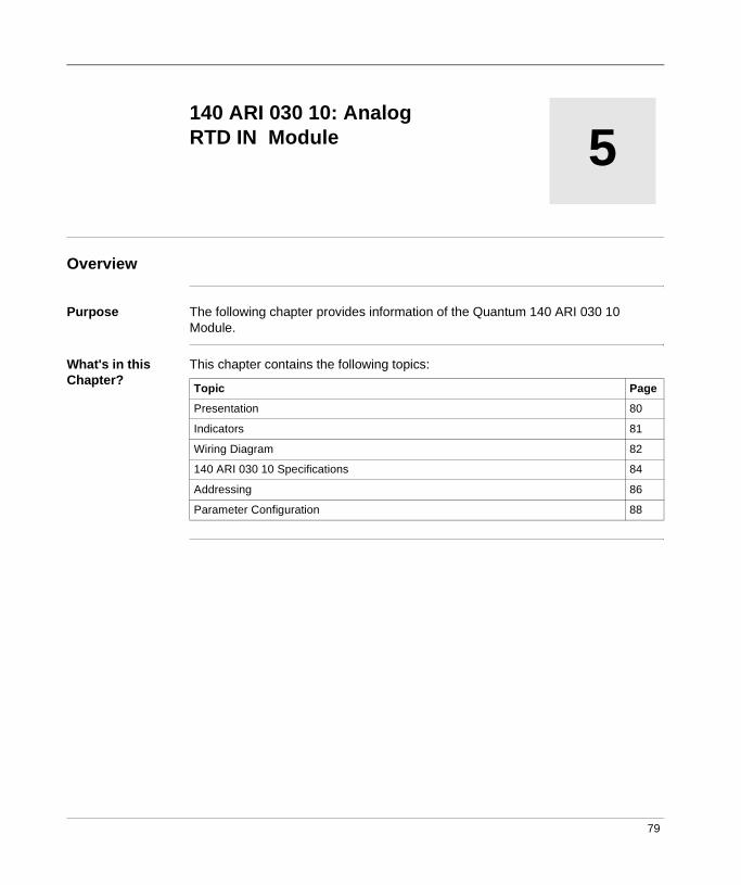
5
140 ARI 030 10: Analog RTD IN ModuleOverview
Purpose The following chapter provides information of the Quantum 140 ARI 030 10 Module.
What's in this Chapter?
This chapter contains the following topics:
Topic Page
Presentation 80
Indicators 81
Wiring Diagram 82
140 ARI 030 10 Specifications 84
Addressing 86
Parameter Configuration 88
79

140 ARI 030 10
Presentation
Function The Analog RTD Input 8 Channel module accepts input from up to eight 2-, 3-, and 4-wire RTD sensors, and provides temperature measurement data to the Quantum CPU.
Illustration The following figure shows the 140 ARI 030 10 module and its components.
1 Model Number, Module Description, Color Code
2 LED Display
3 Fuse Cutouts
4 Field Wiring Terminal Strip
5 Removable Door
6 Customer Identification Label (Fold label and place it inside door)
Note: The field wiring terminal strip (Modicon #140 XTS 002 00) must be ordered separately. (The terminal strip includes the removable door and label.)
140ARI 030 10
X X
XXXXXXXXXXXXXXXXXXXX
XXXXXXXXXXXXXXXXXXXXX
23
6
8
10
1214
16
18
20
21
232527
29
31
3335
37
1
4
7
9
11
13
1517
19
22
24
26
28
30
32
34
3638
1
2
3
4 5
6
80

140 ARI 030 10
Indicators
Illustration The following table shows the LED indicators for the 140 ARI 030 10 module.
Descriptions The following table shows the LED descriptions for the 140 ARI 030 10 module.
Active F
123
4
123
4
R
5
67
8
5
67
8
LEDs Color Indication when ON
Active Green Bus communication is present.
F Red A fault (external to the module) has been detected.
R Module has passed power up diagnostics
1 ... 8 Green The indicated point or channel is turned ON.
1 ... 8 Red There is a fault on the indicated point or channel.This includes broken wire and short circuit conditions.
81

140 ARI 030 10
Wiring Diagram
Illustration The following figure shows the wiring diagram of the 140 ARI 030 10.
I SOURCE 1(+)2
10
4
6
8
12
14
16
18
20
22
24
26
28
30
32
34
36
38
40 39
37
35
33
31
29
27
25
23
21
19
17
15
13
11
9
7
5
3
1I SOURCE 1(-)
V SENSE 1(+) V SENSE 1(-)
I SOURCE 2(+) I SOURCE 2(-)
V SENSE 2(+) V SENSE 2(-)
SHIELD 2 SHIELD 1
I SOURCE 3(+) I SOURCE 3(-)
V SENSE 3(+) V SENSE 3(-)
I SOURCE 4(+) I SOURCE 4(-)
V SENSE 4(+) V SENSE 4(-)
SHIELD 4 SHIELD 3
I SOURCE 5(+) I SOURCE 5(-)
V SENSE 5(+) V SENSE 5(-)
I SOURCE 6(+) I SOURCE 6(-)
SHIELD 6 SHIELD 5
I SOURCE 7(+)
V SENSE 7(+) V SENSE 7(-)
I SOURCE 7(-)
V SENSE 6(+) V SENSE 6(-)
I SOURCE 8(+) I SOURCE 8(-)
V SENSE 8(+) V SENSE 8(-)
SHIELD 8 SHIELD 7
3-WIRE RTD
2-WIRE RTD
4-WIRE RTD
82

140 ARI 030 10
Notes on Wiring Diagram
The module is calibrated per IEC Publication 751 for platinum RTDs: 100 ohms @ 0 degrees C, TCR = 0.00385 ohms/degrees CDIN 43760 for nickel RTDs, American Platinum RTDs: 100 ohms @ 0 degrees C, TCR = 0.00392 ohms/degrees C.Terminals labeled shield are not connected internally. Shields should be grounded at the field device end. When using 2-wire configurations, the temperature equivalent of twice the lead resistance of one leg must be subtracted from the temperature reading.When field wiring the I/O module, the maximum wire size that should be used is 1-14 AWG or 2-16 AWG; the minimum size is 20 AWG.
83

140 ARI 030 10
140 ARI 030 10 Specifications
General Specifications
RTD-Types / Range
Measurement Current
Resolution / Conversion
Isolation
Module Type 8 Channel IN (RTD)
External Power Not required
Bus Current required (Module) 200 mA
Power Dissipation 1 W
I/O map 10 input words
Input Impedance > 10 MΩ
Fault Detection Out of range or 8 red LEDs to indicate broken wire conditions.
IEC Platinum:PT 100, PT 200, PT 500, PT 1000
-200 ... +850 degrees C
American Platinum:PT 100, PT 200, PT 500, PT 1000
-100 ... +450 degrees C
Nickel:N 100, N 200, N 500, N 1000
-60 ... +180 degrees C
PT 100, PT 200, N100, N200 2.5 mA
PT 500, PT 1000, N 500, N 1000 0.5 mA
Resolution 0.1 degree C
Absolute Accuracy Error +/- 0.5% degrees C (25 degrees C)+/- 0.9% degrees C (0 ... 60 degrees C)
Linearity (0 to 60 degrees C) +/- 0.01% of full scale (0 ... 60 degrees C)
Channel to Channel 300 Vpp
Channel to Bus 1780 VAC @ 47 ... 63 Hz for 1 minute2500 VDC
84

140 ARI 030 10
Update Time (all channels)
2-wire4-wire
640 ms
3-wire 1.2 s
85

140 ARI 030 10
Addressing
Flat Addressing This module requires nine contiguous, 16-bit words—eight for input data and one for channel status. The data words formats are as follows.
The following shows the word 9 register.
*A range warning is issued when a channel input exceeds the rated input value. An out-of-range bit is set when a channel input exceeds the rated input value by 2.34% or when a broken wire is sensed on the channel. The warning bit is cleared (if set) when the out-of-range bit is set.
Channel 1 data Word 1
Word 8 Channel 8 data
Input status wordWord 9
1 = Channel 5 out of range or broken wire1 = Channel 6 out of range or broken wire
1 = Channel 7 out of range or broken wire1 = Channel 8 out of range or broken wire
1 2 3 4 5 6 7 10 11 12 13 14 15 168 9
1 = Range warning on channel 8*1 = Range warning on channel 7*
1 = Range warning on channel 6*1 = Range warning on channel 5*
1 = Channel 1 out of range or broken wire1 = Channel 2 out of range or broken wire
1 = Channel 3 out of range or broken wire1 = Channel 4 out of range or broken wire
1 = Range warning on channel 4*1 = Range warning on channel 3*
1 = Range warning on channel 2*
1 = Range warning on channel 1*
86

140 ARI 030 10
Topological Addressing
Topological addresses for the 140ARI03010 Input Module:
Used abbreviations: b = bus, e = equipment (drop), r = rack, m = module slot.
IODDT The 140ARI03010 Input Module uses the T_ANA_IN_VE IODDT:
Used abbreviations: r = rack, m = module slot, c = channel, b = bus, e = equipment (drop).Bus and Drop default to 1 if not specified and can be left off.
I/O Map Status Byte
The I/O map status byte is used by the 140ARI03010 Input Module as follows.
Point I/O Object Comment
Input 1 %IW[\b.e\]r.m.1 Value
%I[\b.e\]r.m.1.1 Broken wire or Out of range
%I[\b.e\]r.m.1.2 Range warning
• • •
Input 8 %IW[\b.e\]r.m.8 Value
%I[\b.e\]r.m.8.1 Broken wire or Out of range
%I[\b.e\]r.m.8.2 Range warning
Status Word %IW[\b.e\]r.m.9 Status of input channels
IODDT Name Object Data Type Name
T_ANA_IN_VE %CH[\b.e\]r.m.c ANA_IN_VWE userdefined
%IWr.m.c.0 Int .VALUE
%Ir.m.c.1 Bool .ERROR
%Ir.m.c.2 Bool .WARNING
Note: In Quantum IODDTs for analog modules and expert modules the data type Bool is used for %I and %Q.
Channel 1 short circuit or out of range
12345678
MSB LSB
Channel 2 short circuit or out of rangeChannel 3 short circuit or out of range
Channel 4 short circuit or out of rangeChannel 5 short circuit or out of range
Channel 6 short circuit or out of rangeChannel 7 short circuit or out of range
Channel 8 short circuit or out of range
87

140 ARI 030 10
Parameter Configuration
Parameter and Default values
Parameter Configuration Window RTD IN 8CH
ConfigParameter Name Value
MAPPING WORD (%IW-3x)1
AUTOMATIC RESTART
1 : Local Qu... 2 : 140 ARI.
CHANNELSCHANNEL1
TASK MAST
INPUTS STARTING ADDRESSINPUTS ENDING ADDRESS 9
DISABLE4 wire
CHANNEL3CHANNEL4
“Pt 100, -200 to 850”
CHANNEL5CHANNEL6CHANNEL7CHANNEL8
WIRETYPE
No
CHANNEL2
MODULE_CONFIGURATIONRESOLUTION
VALUE TYPEOUTPUT UNIT Centigrade
Temp
1.0 Deg
88

140 ARI 030 10
Name Default Value Options Description
Mapping WORD (%IW-3X) -
Inputs Starting Address 1 -
Inputs Ending Address 9 -
Task(Grayed if module in other than local)
MAST FASTAUX0AUX1AUX2AUX3
fixed to MAST if module in other than local
Module_Configuration
Resolution 1.0 Deg 0.1 Deg
Output Unit Centigrade Fahrenheit
Value Type Temp Raw Value
ChannelsChannel1
Disable No Yes
Wire 4 wire 2 wire3 wire
Type "Pt 100, -200 to 850" "Pt 200, -200 to 850""Pt 500, -200 to 850""Pt 1000, -200 to 850""Ni 100, -200 to 850""Ni 200, -200 to 850""Ni 500, -200 to 850""Ni 1000, -200 to 850""R, 0 to 766,66 ohms""R, 0 to 4000 ohms""Apt 100, -100 to 450 ohms""Apt 200, -100 to 450 ohms""Apt 500, -100 to 450 ohms""Apt 1000, -100 to 450 ohms"
Channel2-Channel8 see Channel1
89

140 ARI 030 10
90
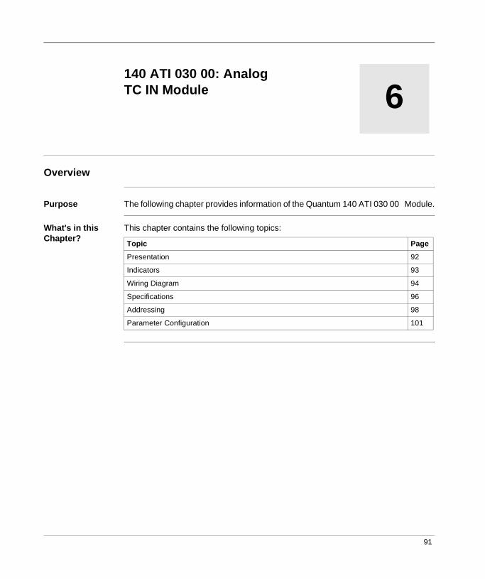
6
140 ATI 030 00: Analog TC IN ModuleOverview
Purpose The following chapter provides information of the Quantum 140 ATI 030 00 Module.
What's in this Chapter?
This chapter contains the following topics:
Topic Page
Presentation 92
Indicators 93
Wiring Diagram 94
Specifications 96
Addressing 98
Parameter Configuration 101
91

140 ATI 030 00
Presentation
Function The140 ATI 030 00 is an eight-channel thermocouple input module.
Illustration The following figure shows the 140 ATI 030 00 module and its components.
1 Model Number, Module Description, Color Code
2 LED Display
3 Fuse Cutouts
4 Field Wiring Terminal Strip
5 Removable Door
6 Customer Identification Label (Fold label and place it inside door)
Note: The field wiring terminal strip (Modicon #140 XTS 002 00) must be ordered separately. (The terminal strip includes the removable door and label.)
140ATI 030 00
X X
XXXXXXXXXXXXXXXXXXXX
XXXXXXXXXXXXXXXXXXXXX
23
6
8
10
1214
16
18
20
21
232527
29
31
3335
37
1
4
7
9
11
13
1517
19
22
24
26
28
30
32
34
3638
1
2
3
4 5
6
92

140 ATI 030 00
Indicators
Illustration The following table shows the LED indicators for the 140 ATI 030 00 module.
Descriptions The following table shows the LED descriptions for the 140 ATI 030 00 module.
Active F
123
4
123
4
5
67
8
5
67
8
LEDs Color Indication when ON
Active Green Bus communication is present.
F Red A fault (external to the module) has been detected.
1 ... 8 Green The indicated point or channel is turned ON.
1 ... 8 Red Indicated channel is out of range.Broken wire condition is detected
93

140 ATI 030 00
Wiring Diagram
Illustration The following figure shows the wiring diagram of the 140 ATI 030 00.
Not used 2
10
4
6
8
12
14
16
18
20
22
24
26
28
30
32
34
36
38
40 39
37
35
33
31
29
27
25
23
21
19
17
15
13
11
9
7
5
3
1
Not used
Not used
Not used
Not used
Not used
Not used
Not used
Not used
Not used
Not used
Not used
Not used
Not used
Not used
Not used
Not used
Not used
Not used
Not used
Not used
Not used
Not used
+
+
+
+
+
+
+
+
-
-
-
-
-
-
-
-
Not used
94

140 ATI 030 00
Notes on Wiring Diagram
Either shielded or unshielded TCs may be used. (The user should consider using shielded wire in a noisy environment.) Shielded types should have a shield tied to earth ground near the signal source end. Connections marked Not Used are not electrically connected within the module. These points are used as a thermal link to ambient air. They are not recommended as electrical tie points as this could affect the accuracy of cold junction compensation.When field wiring the I/O module, the maximum wire size that should be used is 1-14 AWG or 2-16 AWG; the minimum size is 20 AWG.
95
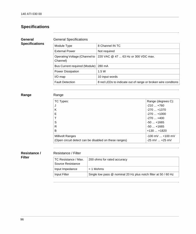
140 ATI 030 00
Specifications
General Specifications
General Specifications
Range Range
Resistance / Filter
Resistance / Filter
Module Type 8 Channel IN TC
External Power Not required
Operating Voltage (Channel to Channel)
220 VAC @ 47 ... 63 Hz or 300 VDC max.
Bus Current required (Module) 280 mA
Power Dissipation 1.5 W
I/O map 10 input words
Fault Detection 8 red LEDs to indicate out of range or broken wire conditons
TC Types:JKETSRB
Range (degrees C):-210 ... +760-270 ... +1370-270 ... +1000-270 ... +400-50 ... +1665-50 ... +1665+130 ... +1820
Millivolt Ranges(Open circuit detect can be disabled on these ranges)
-100 mV ... +100 mV-25 mV ... +25 mV
TC Resistance / Max. Source Resistance
200 ohms for rated accuracy
Input Impedance > 1 Mohms
Input Filter Single low pass @ nominal 20 Hz plus notch filter at 50 / 60 Hz
96

140 ATI 030 00
Noise Rejection / CJC
Noise Rejection / CJC
Resolution Resolution
Absolute Accuracy / Update Time
Absolute Accuracy / Update Time
Isolation Isolation
Notes on Specifications
Absolute accuracy includes all errors from the internal CJC, TC – curvature, offset plus gain, for module temperature of 0 ... 60 degrees C. User supplied TC errors not included. For Type J and K, add 1.5 degrees C inaccuracy for temperatures below -100 degrees C. Type B cannot be used below 130 degrees C.All TC ranges have an open TC detect and upscale output. This results in a reading of 7FFFh or 32767 decimal when an open TC is detected.
Normal Noise Rejection 120 dB min. @ 50 or 60 Hz
Cold Junction Compensation (CJC)
Internal CJC operates 0 ... 60 degrees C (errors are included in the accuracy specification). The connector door must be closed.Remote CJC can be implemented by connecting a TC (which monitors the external junction block temperature) to channel 1. Types J, K, and T are recommended for remote CJC.
TC Ranges 1 degree C (default)0.1 degree C 1 degree F0.1 degree F
Millivolt Ranges 100 mV range , 3.05 μV (16 bit)25 mV range , 0.76 μV (16 bit)
TC Absolute Accuracy (see Note 1)
Types J, K, E, T (see Note 2):+/- 2 degrees C plus +/- 0.1% readingTypes S, R, B (see Note 3):+/- 4 degrees C plus +/- 0.1% reading
Millivolt Absolute Accuracy @ 25 degrees C
+/- 20 microV +/- 0.1% of reading
Accuracy Drift with Temperature
0.15 μV / degrees C + 0.0015% of reading / degrees C max.
Update Time 1 s (all channels)
Channel to Bus 1780 VAC @ 47 ... 63 Hz or2500 VDC for 1 minute
97

140 ATI 030 00
Addressing
Flat Addressing This module requires ten contiguous, 16-bit words—eight for input data, one for channel status, and one for internal temperature of the module. The data words formats are as follows.
The following shows the word 9 register.
* A range warning is issued when a channel input exceeds the rated input value. An out-of-range bit is set when a channel input exceeds the rated input value by 2.4% or when a broken wire is sensed on the channel. The warning bit is cleared (if set) when the out-of-range bit is set.
Channel 1 data Word 1
Word 8 Channel 8 data
Input status wordWord 9
1 = Channel 5 out of range1 = Channel 6 out of range
1 = Channel 7 out of range1 = Channel 8 out of range
1 2 3 4 5 6 7 10 11 12 13 14 15 168 9
1 = Range warning on channel 8*1 = Range warning on channel 7*
1 = Range warning on channel 6*1 = Range warning on channel 5*
1 = Channel 1 out of range1 = Channel 2 out of range
1 = Channel 3 out of range1 = Channel 4 out of range
1 = Range warning on channel 4*1 = Range warning on channel 3*
1 = Range warning on channel 2*
1 = Range warning on channel 1*
98

140 ATI 030 00
The following figure shows the word 10 register.
Topological Addressing
Topological addresses for the 140ATI03000 Input Module:
Used abbreviations: b = bus, e = equipment (drop), r = rack, m = module slot.
IODDT The 140ATI03000 Input Module uses the T_ANA_IN_VWE IODDT:
Used abbreviations: r = rack, m = module slot, c = channel, b = bus, e = equipment (drop).Bus and Drop default to 1 if not specified and can be left off.
Internal temperatureWord 10
Point I/O Object Comment
Input 1 %IW[\b.e\]r.m.1 Value
%I[\b.e\]r.m.1.1 Out of range
%I[\b.e\]r.m.1.2 Range warning
• • •
Input 8 %IW[\b.e\]r.m.8 Value
%I[\b.e\]r.m.8.1 Out of range
%I[\b.e\]r.m.8.2 Range warning
Status Word %IW[\b.e\]r.m.9 Status of input channels
Internal Temperature %IW[\b.e\]r.m.10 Internal module temperature
IODDT Name Object Data Type Name
T_ANA_IN_VWE %CH[\b.e\]r.m.c ANA_IN_VWE userdefined
%IWr.m.c.0 Int .VALUE
%Ir.m.c.1 Bool .ERROR
%Ir.m.c.2 Bool .WARNING
Note: In Quantum IODDTs for analog modules and expert modules the data type Bool is used for %I and %Q.
99

140 ATI 030 00
I/O Map Status Byte
The I/O map status byte is used by the 140ATI03000 Input Module as follows.
Channel 1 open circuit or out of range
12345678
MSB LSB
Channel 2 open circuit or out of rangeChannel 3 open circuit or out of range
Channel 4 open circuit or out of rangeChannel 5 open circuit or out of range
Channel 6 open circuit or out of rangeChannel 7 open circuit or out of range
Channel 8 open circuit or out of range
100
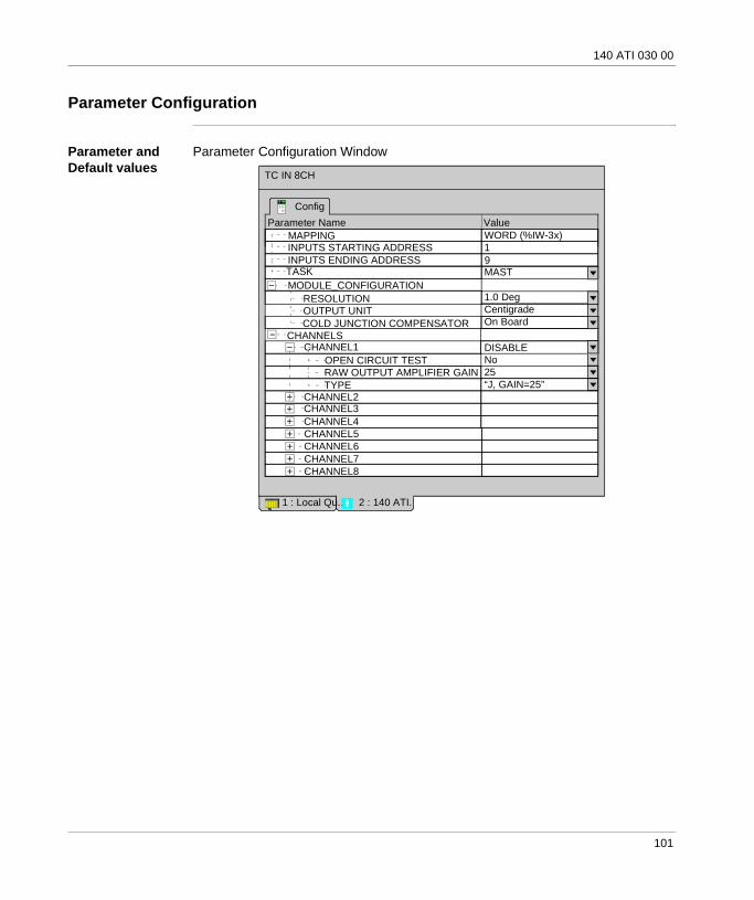
140 ATI 030 00
Parameter Configuration
Parameter and Default values
Parameter Configuration Window
TC IN 8CH
ConfigParameter Name Value
MAPPING WORD (%IW-3x)1
AUTOMATIC RESTART
1 : Local Qu... 2 : 140 ATI.
CHANNELSCHANNEL1
TASK MAST
INPUTS STARTING ADDRESSINPUTS ENDING ADDRESS 9
OPEN CIRCUIT TEST25
CHANNEL3CHANNEL4
“J, GAIN=25”
CHANNEL5CHANNEL6CHANNEL7CHANNEL8
RAW OUTPUT AMPLIFIER GAINTYPE
No
CHANNEL2
MODULE_CONFIGURATIONRESOLUTION
COLD JUNCTION COMPENSATOROUTPUT UNIT Centigrade
On Board
1.0 Deg
DISABLE
101

140 ATI 030 00
Name Default Value Options Description
Mapping WORD (%IW-3X) -
Inputs Starting Address 1 -
Inputs Ending Address 9 -
Task(Grayed if module in other than local)
MAST FASTAUX0AUX1AUX2AUX3
fixed to MAST if module in other than local
Module_Configuration
Resolution 1.0 Deg 0.1 Deg
Output Unit Centigrade Fahrenheit
Cold Junction Compensator On Board Channel 1
Channels
Channel1 DISABLE ENABLE
Open Circuit Test No Yes
Raw Output Amplifier Gain 25 100
Type "J, Gain=25" "K, Gain=25""E, Gain=25""T, Gain=100""S, Gain=100""R, Gain=100"
Channel2-Channel8 see Channel1
102
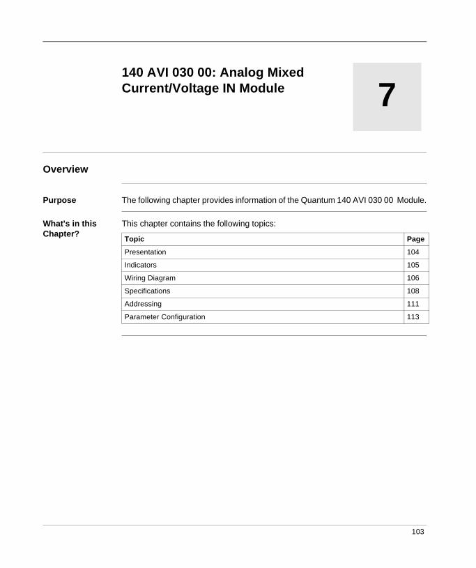
7
140 AVI 030 00: Analog Mixed Current/Voltage IN ModuleOverview
Purpose The following chapter provides information of the Quantum 140 AVI 030 00 Module.
What's in this Chapter?
This chapter contains the following topics:
Topic Page
Presentation 104
Indicators 105
Wiring Diagram 106
Specifications 108
Addressing 111
Parameter Configuration 113
103

140 AVI 030 00
Presentation
Function The Analog In 8 Channel Bipolar module accepts a mix of current and voltage inputs. Jumpers are required between the input and sense terminals for current inputs.
Illustration The following figure shows the 140 AVI 030 00 module and its components.
1 Model Number, Module Description, Color Code
2 LED Display
3 Fuse Cutouts
4 Field Wiring Terminal Strip
5 Removable Door
6 Customer Identification Label (Fold label and place it inside door)
Note: The field wiring terminal strip (Modicon #140 XTS 002 00) must be ordered separately. (The terminal strip includes the removable door and label.)
140AVI 030 00
X X
XXXXXXXXXXXXXXXXXXXX
XXXXXXXXXXXXXXXXXXXXX
23
6
8
10
1214
16
18
20
21
232527
29
31
3335
37
1
4
7
9
11
13
1517
19
22
24
26
28
30
32
34
3638
1
2
3
4 5
6
104

140 AVI 030 00
Indicators
Illustration The following table shows the LED indicators for the 140 AVI 030 00 module.
Descriptions The following table shows the LED descriptions for the 140 AVI 030 00 module.
Active F
123
4
123
4
5
67
8
5
67
8
LEDs Color Indication when ON
Active Green Bus communication is present.
F Red A fault (external to the module) has been detected.
1 ... 8 Green The indicated point or channel is turned ON.
1 ... 8 Red Indicated channel is out of range (1 ... 5 V)Broken wire condition is detected (4 ... 20 mA)
105

140 AVI 030 00
Wiring Diagram
Illustration The following figure shows the 140 AVI 030 00 wiring diagram.
N/C
INPUT
INPUT
N/C
N/C
INPUT
N/C
INPUT
N/C
N/C
INPUT
N/C
INPUT
N/C
N/C
INPUT
INPUT
INPUT
I SENSE
INPUT
INPUT
I SENSE
INPUT
N/C
I SENSE 2
INPUT
INPUT
I SENSE
Jumper
N/C
N/C
N/C
2
10
4
6
8
12
14
16
18
20
22
24
26
28
30
32
34
36
38
40 39
37
35
33
31
29
27
25
23
21
19
17
15
13
11
9
7
5
3
1
I SENSE
N/C
I SENSE
INPUT
N/C
I SENSE
INPUT
I SENSE
N/C
current source
voltage source
-+
+-
106

140 AVI 030 00
Notes on Wiring Diagram
The current and voltage sources are supplied by the user (fusing is at the discretion of the user).Either a shielded or unshielded signal cable may be used. Shielded types should have a shield tied to earth ground near the signal source end.To prevent improper fault indications, unused inputs should have the + (plus) and - (minus) inputs tied together and be configured for a bipolar input range.N / C = Not Connected.When field wiring the I/O module, the maximum wire size that should be used is 1-14 AWG or 2-16 AWG; the minimum size is 20 AWG.
107

140 AVI 030 00
Specifications
General Specifications
General Specifications
Operating Ranges
Operating Ranges
Voltage / Input Voltage / Input
Current / Input Current / Input
Module Type 8 Channel IN Differential
External Power Not required
Operating Voltage (Channel to Channel)
200 VDC135 VAC rms max.
Bus Current required (Module) 280 mA
Power Disssipation 2.2 W
I/O map 9 input words
Fault Detection Broken wire in 4 ... 20 mA mode, Out of range
Bipolar +/- 10 VDC+/- 5 VDC+/- 20 mA
Unipolar 0 ...10 VDC0 ... 5 VDC0 ... 20 mA
Unipolar with Offset 1 ... 5 VDC4 ... 20 mA
Note: The Operating Ranges are selectable on a per-channel base.
Absolute Voltage (max.) 50 VDC
Linear Mesuring Range (Input range) x 1.024
Input Impedance > 20 Mohms
Absolute Current (max.) 25 mA
Linear Measuring Range Input range) x 1.024
Input Impedance 250 ohms + 0.03%
108

140 AVI 030 00
Resolution / Conversion
Resolution / Conversion
Isolation Isolation
16 bit +/- 10 VDC, 0 ...10 VDC
15 bit +/- 5 VDC, 0 ...5 VDC, +/- 20 mA, 0 ... 20 mA
14 bit 1 ... 5 VDC; 4 ... 20 mA
Absolute Accuracy Error @ 25 degrees C (voltage mode)
Typical: +/- 0.03%Maximum: +/- 0.05% of full scale
Accuracy Drift with Temperature Typical: +/- 0.0015% of full scale / degrees CMaximum: +/- 0.004% of full scale / degrees C
Linearity +/- 0.008%
Common Mode Rejection > -80 dB @ 60 Hz
Input Filter Single pole low pass, -3 dB @ 847 Hz, +/- 20%
Update Time 10 ms for all channels
Channel to Bus 500 VAC rms for 1 minute750 VDC rms for 1 minute
Note: Calibration is not required for this module.
109

140 AVI 030 00
Linear Measuring Ranges Table
The following table shows the linear measuring ranges for the 140 AVI 030 00 Analog Input Module.
* The Voltmeter ranges are listed in Modsoft signed format.
Data Format Input Under Warning
Normal Over Warning
16-bit Format +/- 10 V < 768 768 ... 64,768 > 64,768
+/- 5 V, +/- 20 mA < 16,768 16,768 ... 48,768 > 48,768
0 ... 10 V 0 ... 64,000 > 64,000
0 ... 5 V, 0 ... 20 mA 0 ... 32,000 > 32,000
1 ... 5 V, 4 ... 20 mA <6,400 6,400 ... 32,000 > 32,000
Voltmeter* Format
+/- 10 V < -10,000 -10,000 ... 10,000 > 10,000
+/-5 V, +/- 20 mA < -5,000 -5,000 ... 5,000 > 5,000
0 ... 10 V 0 ... 10,000 > 10,000
0 ... 5 V, 0 ... 20 mA 0 ... 5,000 > 5,000
1 ... 5 V, 4 ... 20 mA < 1,000 1,000 ... 5,000 > 5,000
12-bit Format +/- 10 V 0 0 ... 4,095 4,095
+/- 5 V, +/- 20 mA 0 0 ... 4,095 4,095
0 ... 10 V 0 ... 4,095 4,095
0 ... 5 V, 0 ... 20 mA 0 ... 4,095 4,095
1 ... 5 V, 4 ... 20 mA 0 0 ... 4,095 4,095
110

140 AVI 030 00
Addressing
Flat Addressing This module requires nine contiguous, 16-bit words—eight for input data and one for channel status. The data words formats are as follows.
The following shows the word 9 register.
*A range warning is issued when a channel input exceeds the rated input value. Warning bit stay on after out of range bits are set. **An out-of-range bit is set when a channel input exceeds the rated input value by 2.4% or when a broken wire (4 ... 20 mA or 1 ... 5 V mode) is sensed on the channel. Out of range bits are also set if inputs drop below 0.5 V (1 ... 5 V mode) or 2.08 mA (4 ...20 mA mode)
Channel 1 data Word 1
Word 8 Channel 8 data
Input status wordWord 9
1 = Channel 5 out of range or broken wire**1 = Channel 6 out of range or broken wire**
1 = Channel 7 out of range or broken wire**1 = Channel 8 out of range or broken wire**
1 2 3 4 5 6 7 10 11 12 13 14 15 168 9
1 = Range warning on channel 8*1 = Range warning on channel 7*
1 = Range warning on channel 6*1 = Range warning on channel 5*
1 = Channel 1 out of range or broken wire**1 = Channel 2 out of range or broken wire**
1 = Channel 3 out of range or broken wire**1 = Channel 4 out of range or broken wire**
1 = Range warning on channel 4*1 = Range warning on channel 3*
1 = Range warning on channel 2*
1 = Range warning on channel 1*
111

140 AVI 030 00
Topological Addressing
Topological addresses for the 140AVI03000 Input Module:
Used abbreviations: b = bus, e = equipment (drop), r = rack, m = module slot.
IODDT The 140AVI03000 Input Module uses the T_ANA_IN_VWE IODDT:
Used abbreviations: r = rack, m = module slot, c = channel, b = bus, e = equipment (drop).Bus and Drop default to 1 if not specified and can be left off.
I/O Map Status Byte
The I/O map status byte is used by the 140AVI03000 Input Module as follows.
Point I/O Object Comment
Input 1 %IW[\b.e\]r.m.1 Value
%I[\b.e\]r.m.1.1 Out of range
%I[\b.e\]r.m.1.2 Range warning
• • •
Input 8 %IW[\b.e\]r.m.8 Value
%I[\b.e\]r.m.8.1 Out of range
%I[\b.e\]r.m.8.2 Range warning
Status Word %IW[\b.e\]r.m.9 Status of input channels
IODDT Name Object Data Type Name
T_ANA_IN_VWE %CH[\b.e\]r.m.c ANA_IN_VWE userdefined
%IWr.m.c.0 Int .VALUE
%Ir.m.c.1 Bool .ERROR
%Ir.m.c.2 Bool .WARNING
Note: In Quantum IODDTs for analog modules and expert modules the data type Bool is used for %I and %Q.
12345678
MSB LSB
1 = Broken wire on one or more input channels
112

140 AVI 030 00
Parameter Configuration
Parameter and Default values
Parameter Configuration Window
Name Default Value Options Description
Mapping WORD (%IW-3X) -
Inputs Starting Address 1 -
Inputs Ending Address 9 -
Task(Grayed if module in other than local)
MAST FASTAUX0AUX1AUX2AUX3
fixed to MAST if module in other than local
Data Format 16 bit format Volt Meter12 bit format
Channels
Channel1 -10 TO +10V -10V TO +10V0V TO +10V-5V TO +5V0V TO +5V+1V TO +5V-20 mA TO +20mA
Channel2-Channel8 see Channel1
AN IN 8CH BIPOLAR
ConfigParameter Name Value
MAPPING WORD (%IW-3x)1
AUTOMATIC RESTART
1 : Local Qu... 2 : 140 AVI.
CHANNELSCHANNEL1
TASK MAST
INPUTS STARTING ADDRESSINPUTS ENDING ADDRESS 9
CHANNEL3CHANNEL4CHANNEL5CHANNEL6CHANNEL7CHANNEL8
CHANNEL2
DATA FORMAT
-10V TO +10V-10V TO +10V-10V TO +10V-10V TO +10V-10V TO +10V-10V TO +10V-10V TO +10V-10V TO +10V
16 bit format
113

140 AVI 030 00
114

III
Analog OUT ModulesAt a Glance
Introduction The following part provides information on the Quantum Analog OUT modules.
What's in this Part?
This part contains the following chapters:
Chapter Chapter Name Page
8 140 ACO 020 00: Analog Current OUT Module 117
9 140 ACO 130 00: Analog Mixed Current OUT Module 127
10 140 AVO 020 00: Analog Mixed Voltage OUT Module 137
115

Analog OUT Modules
116

8
140 ACO 020 00: Analog Current OUT ModuleOverview
Purpose The following chapter provides information of the Quantum 140 ACO 020 00 Module.
What's in this Chapter?
This chapter contains the following topics:
Topic Page
Presentation 118
Indicators 119
Wiring Diagram 120
Specifications 122
Addressing 124
Parameter Configuration 125
117

140 ACO 020 00
Presentation
Function The Analog Output 4 Channel Current module controls and monitors current in 4 ... 20 mA loops.
Illustration The following figure shows the 140 ACO 020 00 module and its components.
1 Model Number, Module Description, Color Code
2 LED Display
3 Fuse Cutouts
4 Field Wiring Terminal Strip
5 Removable Door
6 Customer Identification Label (Fold label and place it inside door)
Note: The field wiring terminal strip (Modicon #140 XTS 002 00) must be ordered separately. (The terminal strip includes the removable door and label.)
140ACo 020 00
X X
XXXXXXXXXXXXXXXXXXXX
XXXXXXXXXXXXXXXXXXXXX
23
6
8
10
1214
16
18
20
21
232527
29
31
3335
37
1
4
7
9
11
13
1517
19
22
24
26
28
30
32
34
3638
1
2
3
4 5
6
118

140 ACO 020 00
Indicators
Illustration The following table shows the LED indicators for the 140 ACO 020 00 module.
Descriptions The following table shows the LED descriptions for the 140 ACO 020 00 module.
Active F
12
1
2
34
3
4
LEDs Color Indication when ON
Active Green Bus communication is present.
F Red A fault (external to the module) has been detected.
1 ... 4 Green Module outputs switched ON.
1 ... 4 Red Broken wire on indicated channels.
Note: When the green channel status LEDs are OFF, the loop current is 0 mA .
119

140 ACO 020 00
Wiring Diagram
Illustration The following figure shows the wiring diagram for the 140 ACO 020 00 module.
2
10
4
6
8
12
14
16
18
20
22
24
26
28
30
32
34
36
38
40 39
37
35
33
31
29
27
25
23
21
19
17
15
13
11
9
7
5
3
1I SOURCE 1(-)
N/C
N/C
N/C
N/C
MONITOR 1(+)
I SOURCE 1(-)
N/C
I SOURCE 1(-)
I SOURCE 2(-)
I SOURCE 2(-)
N/C
I SOURCE 2(-)
I SOURCE 3(-)
I SOURCE 3(-)
N/C
I SOURCE 3(-)
I SOURCE 4(-)
I SOURCE 4(-)
N/C
I SOURCE 4(-)
VM
N/C
N/C
N/CI SINK 1(+)
MONITOR 2(+)
N/C
N/C
N/CI SINK 2(+)
MONITOR 3(+)
N/C
N/C
N/C
I SINK 3(+)
MONITOR 4(+)
N/C
N/C
N/CI SINK 4(+)
- +
FIELD DEVICE
FIELD DEVICE
+ -
-
+
+-
-
+
LOOP SUPPLY
120

140 ACO 020 00
Notes on Wiring Diagram
Unused channels will indicate broken wire status unless wired to the loop supply, as shown on Channel 4. In this example, loop supply must be 30 V or less.VM is an optional voltmeter that can be connected to read voltage that is proportional to the current. Wiring to this terminal is limited to 1 meter maximum.The wiring example shows Channel 1 acting as a current sink and Channel 2 acting as a current source for their respective field devices.N / C = Not Connected.At power up, the channel outputs are all disabled (current = 0). Configuring any channel as disabled will cause all channels to be disabled when a communication loss occurs.When field wiring the I/O module, the maximum wire size that should be used is 1-14 AWG or 2-16 AWG; the minimum size is 20 AWG.
WARNING
Possible injury to personnel or equipment.
Before removing the connector, ensure that it is safe to have field wiring in an open circuit condition.
Failure to follow this precaution can result in death, serious injury, or equipment damage.
121

140 ACO 020 00
Specifications
General Specifications
General Specifications
Voltage Voltage
Resolution / Conversion
Resolution
Module Type 4 Channel OUT
External Power Loop Voltage:12 ... 30 VDC, up to 60 VDC with an external loop resistor
Bus Current required (Module) 480 mA
Power Dissipation 5.3 W max.
I/O map 4 output words
Fault Detection Open circuit in 4 ... 20 mA mode. Specific channel is identified when an open circuit is detected through the red channel LED.
Loop Voltage 12 ... 30 VDC, up to 60 VDC with an external loop resistor
Loop Resistance * = ( - 30 VDC) / 0.02 A
= ( - 7 VDC) / 0.02 A
* No is required for loop voltage less than 30 VDC
Internal Voltage Drop 7 VDC min., 30 VDC max. @ 20 mA
RMIN VLOOP
RMAX VLOOP
RMIN
Resolution 12 bit
Accuracy Error at 25 degrees C +/- 0.20% of full scale
Accuracy Drift with Temperature Typical: 0.004% of full scale / degrees C.Maximum: 0.007% of full scale / degrees C.
Linearity +/- 1 LSB
Update Time 3 ms for all Channels (simultaneous update)
Settling time 900 μs to +/- 0.1 % of final value
122

140 ACO 020 00
Isolation Isolation
Fuses Fuses
Voltmeter Monitor Specifications Table
The following table shows the voltmeter monitor specifications.
Channel to Bus
1780 VAC @ 47 ... 63 Hz or2500 VDC for 1 minute
Channel to Channel
500 VAC @ 47 ... 63 Hz or750 VDC for 1 minute
Internal Not required
External -
Note: When the green channel status LEDs are off, the loop current is 0 mA.
Range 1 ... 5 V (Main current loop must be active)
Scaling (Volts) = (mA) x 0.25
Output Impedance 300 ohms Typical
Wiring Length 1 m max.
VOUT ILOOP
123

140 ACO 020 00
Addressing
Flat Addressing This module requires four contiguous, 16-bit words (%MW) for output data. The data words formats are as follows.
Topological Addressing
Topological addresses for the 140ACO02000 Output Module:
Used abbreviations: b = bus, e = equipment (drop), r = rack, m = module slot.
I/O Map Status Byte
The I/O map status byte is used by the 140ACO02000 Output Module as follows.
Channel 1 data Word 1
Word 4 Channel 4 data
Point I/O Object Comment
Output 1 %QW[\b.e\]r.m.1 Value
Output 2 %QW[\b.e\]r.m.2 Value
Output 3 %QW[\b.e\]r.m.3 Value
Output 4 %QW[\b.e\]r.m.4 Value
Channel 1 loop broken wire
12345678
MSB LSB
Channel 2 loop broken wireChannel 3 loop broken wiree
Channel 4 loop broken wire
124

140 ACO 020 00
Parameter Configuration
Parameter and Default values
Parameter Configuration Window
Name Default Value Options Description
Mapping WORD (%MW-4X) -
Outputs Starting Address 1 -
Outputs Ending Address 4 -
Task(Grayed if module in other than local)
MAST FASTAUX0AUX1AUX2AUX3
fixed to MAST if module in other than local
Channels
Channel1 LAST VALUE DISABLEDUSER DEFINED
Timeout Value 0 0-65535 only enabled if Channel=USER DEFINED
Channel2-Channel4 see Channel1
AN OUT 4CH CURR
ConfigParameter Name Value
MAPPING WORD (%MW-4x)1
AUTOMATIC RESTART
1 : Local Qu... 2 : 140 ACO.
CHANNELSCHANNEL1
TASK MAST
OUTPUTS STARTING ADDRESSOUTPUTS ENDING ADDRESS 4
TIMEOUT VALUELAST VALUE
CHANNEL2CHANNEL3CHANNEL4
0LAST VALUELAST VALUELAST VALUE
125

140 ACO 020 00
126

9
140 ACO 130 00: Analog Mixed Current OUT ModuleOverview
Purpose The following chapter provides information of the Quantum 140 ACO 130 00 Module.
What's in this Chapter?
This chapter contains the following topics:
Topic Page
Presentation 128
Indicators 129
Wiring Diagram 130
Specifications 132
Addressing 134
Parameter Configuration 135
127

140 ACO 130 00
Presentation
Function The 140 ACO 130 00 is an eight channel analog output module used to control and monitor current in 4 ... 20 mA, 0 ... 20 mA, and 0 ... 25 mA loops.
Illustration The following figure shows the 140 ACO 130 00 module and its components.
1 Model Number, Module Description, Color Code
2 LED Display
3 Fuse Cutouts
4 Field Wiring Terminal Strip
5 Removable Door
6 Customer Identification Label (Fold label and place it inside door)
Note: The field wiring terminal strip (Modicon #140 XTS 002 00) must be ordered separately. (The terminal strip includes the removable door and label.)
140ACO 130 00
X X
XXXXXXXXXXXXXXXXXXXX
XXXXXXXXXXXXXXXXXXXXX
23
6
8
10
1214
16
18
20
21
232527
29
31
3335
37
1
4
7
9
11
13
1517
19
22
24
26
28
30
32
34
3638
1
2
3
4 5
6
128

140 ACO 130 00
Indicators
Illustration The following table shows the LED indicators for the 140 ACO 130 00 module.
Descriptions The following table shows the LED descriptions for the 140 ACO 130 00 module.
Active F
123
4
123
4
5
67
8
5
67
8
LEDs Color Indication when ON
Active Green Bus communication is present.
F Red A fault (external to the module) has been detected.
1 ... 8 Green Module outputs switched ON.
1 ... 8 Red Broken wire on indicated channels.
129

140 ACO 130 00
Wiring Diagram
Illustration 140 ACO 130 Wiring Diagram
RETURN
OUTPUT 8 SINK
MONITOR
OUTPUT 7 SINK
OUTPUT 6 SINK
OUTPUT 5
OUTPUT 4
OUTPUT 3
OUTPUT 2
OUTPUT 1
RETURN MONITOR
NC
NC
NC
NC
NC
NC
NC
NC
NC
NC
2
10
4
6
8
12
14
16
18
20
22
24
26
28
30
32
34
36
38
40 39
37
35
33
31
29
27
25
23
21
19
17
15
13
11
9
7
5
3
1
NC
MONITOR
NC
MONITOR
MONiTOR
MONITOR
MONITOR
MONITOR
NC
RETURN
NC
RETURN
RETURN
NC
RETURN
RETURN
NC
RETURN
VM
Field Device
Field Device
Field Device
Field Device
Field Device
Field Device
Field Device
Field Device
VMVM24 Vdc
loopsupply
+
-
130

140 ACO 130 00
Notes on Wiring Diagram
At power up all channel outputs have zero current (0 mA).VM is an optional voltmeter that can be connected to read voltage that is proportional to the current. Wiring to this terminal is limited to 1 meter maximum.Either shielded or unshielded cables may be used. In noisy environments twisted shielded cable is recommended. Shielded cable should have a shield tied to earth ground near the signal source end.Unused inputs may cause the activation of the F (fault) LED. To avoid this occurrence the unused channels should be configured in the 0 ... 25 mA range.All terminals labeled ‘RETURN" are common inside the module.N/C = Not connectedWhen field wiring the I/O module, the maximum wire size that should be used is 1-14 AWG or 2-16 AWG; the minimum size is 20 AWG.
131

140 ACO 130 00
Specifications
General Specifications
General Specifications
Voltage Voltage
Range / Resolution
Range / Resolution
Accuracy Accuracy
Linearity Linearity
Module Type 8 Channel OUT
External Power Loop Voltage: 6 ... 30 VDC max.
Bus Current required (Module) 550 mA
Power Dissipation 5.0 W max.
I/O map 8 output words
Fault Detection Open circuit in 4 ... 20 mA mode. The faulty channel is detected through the red channel LED and is also reported back to the controller in the I/O Map status byte
Loop Voltage 6 ... 30 VDC max.
Internal Voltage Drop 6 VDC min., 30 VDC max. @ 25 mA
0 ... 25 mA 0 ... 25,000 counts
0 ... 20 mA 0 ... 20,000 counts
4 ... 20 mA 0 ... 16,000 counts
4 ... 25 mA 0 ... 4,095 counts
Accuracy Error @ 25 degrees C +/- 0.20% of full scale
Accuracy Drift with Temperature Typical: 0.004% of full scale / degrees C.Maximum: 0.007% of full scale / degrees C.
0 ... 25 mA0 ... 20 mA4 ... 20 mA
+/- 4 μA
4 ... 25 mA +/- 12 μA
132

140 ACO 130 00
Times Times
Isolation Isolation
Fuses Fuses
Update Time 5 ms for all Channels
Settling Time Full Scale 1.6 ms to 5% of the final value
Step Change 3.2 ms to 5% of the final value
Field to Bus 1780 VAC for 1 minute
Channel to Channel None
Internal None
External None
133
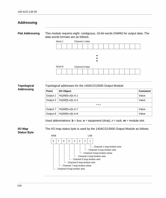
140 ACO 130 00
Addressing
Flat Addressing This module requires eight contiguous, 16-bit words (%MW) for output data. The data words formats are as follows.
Topological Addressing
Topological addresses for the 140ACO13000 Output Module:
Used abbreviations: b = bus, e = equipment (drop), r = rack, m = module slot.
I/O Map Status Byte
The I/O map status byte is used by the 140ACO13000 Output Module as follows.
Channel 1 data Word 1
Word 8 Channel 8 data
Point I/O Object Comment
Output 1 %QW[\b.e\]r.m.1 Value
Output 2 %QW[\b.e\]r.m.2 Value
• • •
Output 7 %QW[\b.e\]r.m.7 Value
Output 8 %QW[\b.e\]r.m.8 Value
Channel 1 loop broken wire
12345678
MSB LSB
Channel 2 loop broken wireChannel 3 loop broken wiree
Channel 4 loop broken wireChannel 5 loop broken wire
Channel 6 loop broken wireChannel 7 loop broken wiree
Channel 8 loop broken wire
134

140 ACO 130 00
Parameter Configuration
Parameter and Default values
Parameter Configuration Window
Name Default Value Options Description
Mapping WORD (%MW-4X) -
Outputs Starting Address 1 -
Outputs Ending Address 8 -
Task(Grayed if module in other than local)
MAST FASTAUX0AUX1AUX2AUX3
fixed to MAST if module in other than local
ChannelsChannel1
Range Selection "4 ... 20 mA, 0-4095" "4 ... 20 mA, 0-16000""0 ... 20 mA, 0-20000""0 ... 25 mA, 0-25000"
Timeout State LAST VALUE MINIMUM OUTPUTUSER DEFINED
Timeout Value 0 0-65535 only enabled Timeout State=USER DEFINED
Channel2-Channel8 see Channel1
AN OUT 8CH CURR
ConfigParameter Name Value
MAPPING WORD (%MW-4x)1
AUTOMATIC RESTART
1 : Local Qu... 2 : 140 ACO.
CHANNELSCHANNEL1
TASK MAST
OUTPUTS STARTING ADDRESSOUTPUTS ENDING ADDRESS 8
RANGE SELECTIONLAST VALUE
CHANNEL2CHANNEL3CHANNEL4
0
CHANNEL5CHANNEL6CHANNEL7CHANNEL8
TIMEOUT STATETIMEOUT VALUE
“0 ... 20 mA, 0-4095”
135

140 ACO 130 00
136

10
140 AVO 020 00: Analog Mixed Voltage OUT ModuleOverview
Purpose The following chapter provides information of the Quantum 140 AVO 020 00 Module.
What's in this Chapter?
This chapter contains the following topics:
Topic Page
Presentation 138
Indicators 139
Wiring Diagram 140
Specifications 142
Addressing 144
Parameter Configuration 145
137

140 AVO 020 00
Presentation
Function The Analog Out 4 Channel module accepts outputs voltages in mixed modes and levels. These are selected using jumpers on the field-wiring connector.
Illustration The following figure shows the 140 AVO 020 00 module and its components.
1 Model Number, Module Description, Color Code
2 LED Display
3 Fuse Cutouts
4 Field Wiring Terminal Strip
5 Removable Door
6 Customer Identification Label (Fold label and place it inside door)
Note: The field wiring terminal strip (Modicon #140 XTS 002 00) must be ordered separately. (The terminal strip includes the removable door and label.)
140AVO 020 00
X X
XXXXXXXXXXXXXXXXXXXX
XXXXXXXXXXXXXXXXXXXXX
23
6
8
10
1214
16
18
20
21
232527
29
31
3335
37
1
4
7
9
11
13
1517
19
22
24
26
28
30
32
34
3638
1
2
3
4 5
6
138

140 AVO 020 00
Indicators
Illustration The following table shows the LED indicators for the 140 AVO 020 00 module.
Descriptions During normal operation, the front panel Active and 1 ... 4 green LEDs are ON. If bus communication to the module stops for any reason, the Active LED will go off and output values are set depending on panel software configuration.
When LEDs 1 ... 4 are ON, the channel output levels will be as predetermined and held by the module.When LEDs 1 ... 4 are OFF, the master override levels are output on each channel.
Active
12
3
4
139

140 AVO 020 00
Wiring Diagram
Illustration The following figure shows the wiring diagram for the 140 AVO 020 00 module.
COMMON 1 (-)
COMMON 1 (-)
MASTER OVERRIDE
N/C
COMMON 1 (-)
COMMON 2 (-)
COMMON 2 (-)
MASTER OVERRIDE
N/C
COMMON 2 (-)
COMMON 3 (-)
COMMON 3 (-)
MASTER OVERRIDE
N/C
COMMON 3 (-)
COMMON 4 (-)
COMMON 4 (-)
MASTER OVERRIDE
N/C
COMMON 4 (-)
SeeNOTE 1
SeeNOTE 1
SeeNOTE 1
SeeNOTE 1
OUTPUT 1 (+)
R 1
N/C
OUTPUT 2 (+)
CONTROL 1
REFERENCE 1
Jumper
JumperR 2
Jumper
CONTROL 2REFERENCE 2
N/C
OUTPUT 3 (+)
Jumper
R 3CONTROL 3
Jumper
REFERENCE 3
N/C
OUTPUT 4 (+)
Jumper
R 4
CONTROL 4
REFERENCE 4
N/C
1/16A
EXTERNALVOLTAGESOURCE
The external voltage sourceis not required for standardoperation (see NOTE 1).
FIELDDEVICE
FIELDDEVICE
CHANNEL 4JUMPERED
FOR 0 TO 10 V
CHANNEL 3JUMPEREDFOR +/-5 V
CHANNEL 2JUMPERED
FOR 0 TO 5 V
CHANNEL 1JUMPEREDFOR +/-10 V
NOTE 1: Master override is an inputconnected via an internal relay contact to theoutput when the module is not active. Ifconnected to an external source, the masteroverride input must be fused by a 1/16 A fuse.If the master override is not connected to anexternal source, then it must be connected tocommon of that channel. The master overriderelay transition time is typically 2 ms.
NOTE 2: N/C = Not Connected
Normally Open whenCH X green LED is ON
NormallyOpen
NormallyClosed
ChannelOutput X
MasterOverride X
Typical oneof four
Master Override Relay Circuit (Internal)
2 1
4 3
56
8 7
10 9
12 11
1314
16 15
1718
20 19
2122
24 23
2526
28 27
2930
32 31
3334
36 35
3738
40 39
140

140 AVO 020 00
If module power is lost or the module fails, the master override levels will be output.The master override inputs must be from an external supply with a source impedance of < 200 ohms or tied to system common. These inputs for channels that are in use should not be allowed to float and may be unique for each.
WARNINGPossible injury to personnel or equipment.Before removing the connector, ensure that it is safe to have field wiring in an open circuit condition.Failure to follow this precaution can result in death, serious injury, or equipment damage.
WARNINGMalfunction of equipmentMaster override must be connected to an external source through 1/16 A in line fuse, or strapped to common to avoid erroneous outputs in this module.Failure to follow this precaution can result in death, serious injury, or equipment damage.
Note: The output levels of this module are either those generated within the module based on data inputs from the system, or from the master override inputs on the field-wiring terminal strip.
Note: When field wiring the I/O module, the maximum wire size that should be used is 1-14 AWG or 2-16 AWG; the minimum size is 20 AWG.
141

140 AVO 020 00
Specifications
General Specifications
General Specifications
Output Ranges* Output Ranges*
Resolution / Accuracy
Resolution / Accuracy
Accuracy Drift with Temperature
Accuracy Drift with Temperature
Module Type 4 Channel OUT
External Power Not required
Bus Current required (Module) 700 mA
Power Dissipation 4.5 W max.
I/O map 4 output words
Fault Detection None
Wiring length 400 m max.
Voltages (Bipolar) +/- 10 VDC (Min. load resistance = 1 kohms)+/- 5 VDC (Min. load resistance = 500 ohms)
Voltages (Unipolar) 0 ...10 VDC (Min. load resistance = 1 kohms)0 ... 5 VDC (Min. load resistance = 500 ohms)
Output Current +/- 10 mA max. (any range)Outputs are shortcut proof
Source Resistance 0.1 ohms
Note: *The range is determined by Jumpers (see wiring diagram)
Resolution 12 bit
Accuracy Error @ 25 degrees C +/- 0.15% of full scale
Linearity +/- 1 LSB
Unipolar Ranges Typical: 0.003% of full scale / degrees CMaximum: 0.005% of full scale / degrees C
Bipolar Ranges Typical: 0.004% of full scale / degrees CMaximum: 0.007% of full scale / degrees C
142

140 AVO 020 00
Times Times
Isolation Isolation
Fuses Fuses
Max. Settling Time 700 μs to +/- 0.1% of the final value
Update Time 3 ms for all channels
Channel to Bus 1780 VAC rms for 1 minute
Channel to Channel 500 VAC rms for 1 minute
Internal Not required
External An external fuse is required on the master override signal when it is connected to an external source. The required fuse is 1/16 A or 0.063 A fuse:Fuse Type: 3 AG Fast acting 1/16 A, 250 VFuse Holder: 3 AG Fuse typeThe external fuse is not required if master override is connected to common
143

140 AVO 020 00
Addressing
Flat Addressing This module requires four contiguous, 16-bit words (%MW) for output data. The data words formats are as follows.
Topological Addressing
Topological addresses for the 140AVO02000 Output Module:
Used abbreviations: b = bus, e = equipment (drop), r = rack, m = module slot.
I/O Map Status Byte
There is no I/O map status byte used by the 140AVO02000 Output Module.
Channel 1 data Word 1
Word 4 Channel 4 data
Point I/O Object Comment
Output 1 %QW[\b.e\]r.m.1 Value
Output 2 %QW[\b.e\]r.m.2 Value
Output 3 %QW[\b.e\]r.m.3 Value
Output 4 %QW[\b.e\]r.m.4 Value
144
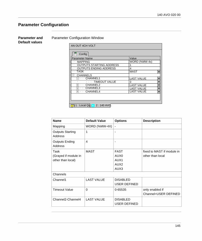
140 AVO 020 00
Parameter Configuration
Parameter and Default values
Parameter Configuration Window
Name Default Value Options Description
Mapping WORD (%MW-4X) -
Outputs Starting Address
1 -
Outputs Ending Address
4 -
Task(Grayed if module in other than local)
MAST FASTAUX0AUX1AUX2AUX3
fixed to MAST if module in other than local
Channels
Channel1 LAST VALUE DISABLEDUSER DEFINED
Timeout Value 0 0-65535 only enabled if Channel=USER DEFINED
Channel2-Channel4 LAST VALUE DISABLEDUSER DEFINED
AN OUT 4CH VOLT
ConfigParameter Name Value
MAPPING WORD (%MW-4x)1
AUTOMATIC RESTART
1 : Local Qu... 2 : 140 AVO.
CHANNELSCHANNEL1
TASK MAST
OUTPUTS STARTING ADDRESSOUTPUTS ENDING ADDRESS 4
TIMEOUT VALUELAST VALUE
CHANNEL2CHANNEL3CHANNEL4
0LAST VALUELAST VALUELAST VALUE
145

140 AVO 020 00
146

IV
Analog IN / OUT ModulesAt a Glance
Introduction The following part provides information on the Quantum Analog IN / OUT modules.
What's in this Part?
This part contains the following chapters:
Chapter Chapter Name Page
11 140 AMM 090 00: Analog Mixed Current/Voltage IN / OUT Module 149
147

Analog IN / OUT Modules
148

11
140 AMM 090 00: Analog Mixed Current/Voltage IN / OUT ModuleOverview
Purpose The following chapter provides information of the Quantum 140 AMM 090 00 Module.
What's in this Chapter?
This chapter contains the following topics:
Topic Page
Presentation 150
Indicators 151
Wiring Diagram 152
Specifications 154
Addressing 157
Parameter Configuration 160
149

140 AMM 090 00
Presentation
Function The Analog In/Out 4/2 bi-directional module combines four analog inputs which accept a mix of current and voltage, with two isolated analog outputs that control and monitor current in 4 ... 20 mA loops.
Illustration The following figure shows the 140 AMM 090 00 module and its components.
1 Model Number, Module Description, Color Code
2 LED Display
3 Fuse Cutouts
4 Field Wiring Terminal Strip
5 Removable Door
6 Customer Identification Label (Fold label and place it inside door)
Note: The field wiring terminal strip (Modicon #140 XTS 002 00) must be ordered separately. (The terminal strip includes the removable door and label.)
140AMM 090 00
X X
XXXXXXXXXXXXXXXXXXXX
XXXXXXXXXXXXXXXXXXXXX
23
6
8
10
1214
16
18
20
21
232527
29
31
3335
37
1
4
7
9
11
13
1517
19
22
24
26
28
30
32
34
3638
1
2
3
4 5
6
150

140 AMM 090 00
Indicators
Illustration The following table shows the LED indicators for the 140 AMM 090 00 module.
Descriptions The following table shows the LED descriptions for the 140 AMM 090 00 module.
Active F
12
1
2
123
4
LEDs Color Indication when ON
Active Green Bus communication is present.
F Red No power applied to the output group(s) or input out of range
1 ... 2 Green (left column)
Module outputs switched ON.
1 ... 2 Red (middle column)
Broken wire on indicated output channels.
1 ... 4 Red (right column)
Indicates input status: under/over range
151

140 AMM 090 00
Wiring Diagram
Illustration The following figure shows the wiring diagram for the 140 AMM 090 00 analog input/output module.
2
4
6
8
12
14
16
18
20 19
17
15
13
11
9
7
5
3
1
22
24
26
28
30
32
34
36
38
40 39
37
35
33
31
29
27
25
23
21
CURRENT SOURCE(-)1
CURRENT SOURCE(-)1
N/C
N/C
CURRENT SOURCE(-)1
CURRENT SOURCE(-)2
CURRENT SOURCE(-)2
N/C
N/C
CURRENT SOURCE(-)2
IN(-)1
N/C
IN(-)2
N/C
N/C
IN(-)3
N/C
IN(-)4
N/C
N/C N/C
SENSE 4
IN(+)4
SENSE 3
IN(+)3
N/C
SENSE 2
IN(+)2
SENSE 1
CURRENT SINK(+)2N/C
N/C
N/C
MONITOR 2
CURRENT SINK(+)1
N/C
N/C
N/C
MONITOR 1 + –
Optional Monitor Voltmeter1 V= 4 mA5 V= 20 mA 24 Vdc
FieldSupply
Field Device
Field Device
4 - 20 mA Current
4 - 20 mA Current
IN(+)1
–
+Sensor 0 - 10 V Output
+
_
10
V
152

140 AMM 090 00
The following information pertains to the wiring diagram above.Output Section 2 Channels
Input Section 4 Channels
Typical Wiring Outputs
Channel 1 The output shows a connection to an external field device and optional monitor.
Channel 2 The output shows a connection to an external field device and the input of channel 1.
Typical Wiring Inputs
Channel 1 Channel 1 shows 4 - 20 mA current input controlled by output section Channel 2.
Channel 2 The input shows a connection to a voltage output sensor.
Note: Pins 1 ... 20 are outputs.Pins 21 ... 40 are inputs.N / C = Not ConnectedJumpers are required between IN (+) and SENSE terminals for all current input ranges.
Note: When field wiring the I/O module, the maximum wire size that should be used is 1-14 AWG or 2-16 AWG; the minimum size is 20 AWG.
CAUTIONPossible Equipment FailureWhen configured for voltage inputs (no jumper installed between In(+) and sense terminals), in the occurrence of field wire breakage, readings will be non-zero and unpredictable.Failure to follow this precaution can result in injury or equipment damage.
153

140 AMM 090 00
Specifications
General Specifications
General Specifications
Operating Ranges
Operating Ranges
Voltage / Input Voltage / Input
Current / Input Current / Input
When configured for current inputs (jumper installed between IN(+) and SENSE terminals), a broken field wire results in a zero current reading. If 4 ... 20 mA is selected, fault LEDs and warning/out of range are displayed.
Module Type 4 Channel IN2 Channel OUT (isolated)
External Power Loop Voltage:... 30 VDC, up to 60 VDC with an external resistor
Bus Current required (Module) 350 mA
Fault Detection Open circuit in 4 ... 20 mA range, or over range, or under range in bipolar modes only.
Bipolar +/- 10 VDC+/- 5 VDC+/- 20 mA
Unipolar 0 ...10 VDC0 ... 5 VDC0 ... 20 mA
Unipolar with Offset
1 ... 5 VDC4 ... 20 mA
Operating Voltage (Channel to Channel) +/- 40 VDC (max.)
Absolute Voltage (max.) +/- 50 VDC
Linear Mesuring Range 2.4% over and under range
Input Impedance in Range > 10 Mohms
Input Impedance over Range < 0.5 Mohms
Absolute Current (max.) +/- 25 mA
Linear Measuring Range 2.4% over and -9.6% under range.
Input Impedance 250 ohms
154

140 AMM 090 00
Resolution / Conversion
Resolution / Conversion
Isolation Isolation
Fuses Fuses
16 bit +/- 10 VDC, 0 ...10 VDC
15 bit +/- 5 VDC, 0 ...5 VDC, +/- 20 mA, 0 ... 20 mA
14 bit 1 ... 5 VDC; 4 ... 20 mA
Absolute Accuracy Error @ 25 degrees C (voltage mode)
Typical: +/- 0.03%Maximum: +/- 0.05% of full scale
Linearity Monotonic +/- 1 LSB
Offset 0 ... 60 degrees C +/- 0.0014% of full scale max.
Gain Shift 0 ... 60 degrees C +/- 0.002% of full scale max.
Common Mode Rejection Better than 80 dB @ 50 or 60 Hz
Input Filter Single pole low pass, -3 dB @ 21 Hz, +/- 20%
Update Time 320 ms for 4 channels
Channel to Bus 500 VAC rms for 1 minute750 VDC rms for 1 minute
Channel to Channel
500 VAC rms for 1 minute750 VDC rms for 1 minute
Internal Not required
External User discretion
155

140 AMM 090 00
Output Specifications
Output Specifications
Resolution / Conversion
Resolution / Conversion
A range warning is issued when a channel input is outside the rated input value. Warning bits stay on after out of range bits are set. An out-of-range bit is set when a channel input exceeds the rated input value by 2.4%. Out of range bits are also set if inputs drop below 0.5V (1 ... 5V mode) or 2.08 mA (4 ... 20 mA mode)
Isolation Isolation
Voltmeter Monitor Specifications Table
The following table shows the specifications for the voltmeter monitor for the analog input/output module.
Loop Voltage ... 30 VDC, up to 60 VDC with an external resistor
Loop Resistance * = ( - 30 VDC) / 0.020 A
= ( - 7 VDC) / 0.020 A
* No is required for loop voltage less than 30 VDC
Internal Voltage Drop 7 VDC min., 30 VDC max. @ 20 mA
Fault Detection Open circuit in 4 ... 20 mA range, or over range, or under range in bipolar modes only.
RMIN VLOOP
RMAX VLOOP
RMIN
Resolution 12 bit
Accuracy Error at 25 degrees C +/- 0.20% of full scale
Accuracy Error @ 0 ...60 degrees C (voltage mode)
Typical: +/- 0.004% of full scaleMaximum: +/- 0.07% of full scale
Linearity Monotonic +/- 1 LSB
Update Time 15 ms for 2 Channels
Settling time 900 micro sec to +/- 0.1 % of final value
Fault Detection Open circuit indicator light and status byte
Channel to Bus 500 VAC rms for 1 minute750 VDC rms for 1 minute
Channel to Channel 500 VAC rms for 1 minute750 VDC rms for 1 minute
Range 1 ... 5 V (Loop current must be active)
Scaling (mA) x 0.250 = (volts)
Output Impedance 300 ohms typical
Maximum Wire Length 1 meter
IOUT VOUT
156
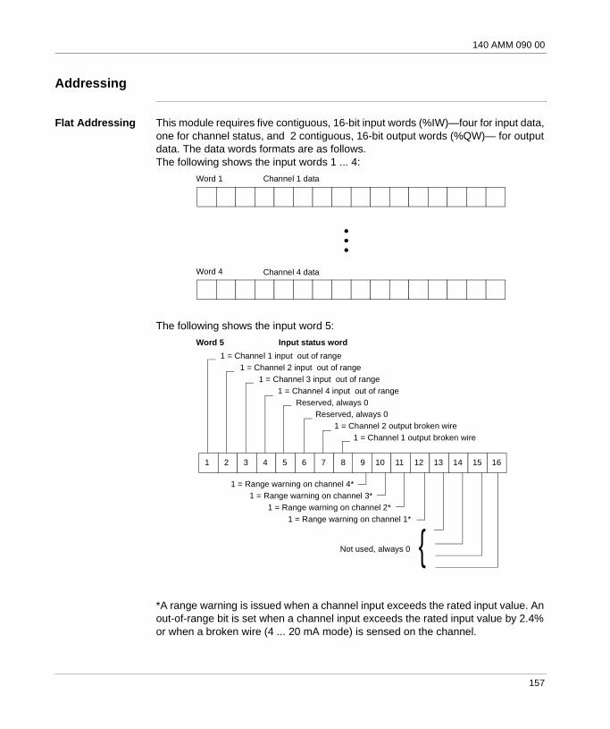
140 AMM 090 00
Addressing
Flat Addressing This module requires five contiguous, 16-bit input words (%IW)—four for input data, one for channel status, and 2 contiguous, 16-bit output words (%QW)— for output data. The data words formats are as follows.The following shows the input words 1 ... 4:
The following shows the input word 5:
*A range warning is issued when a channel input exceeds the rated input value. An out-of-range bit is set when a channel input exceeds the rated input value by 2.4% or when a broken wire (4 ... 20 mA mode) is sensed on the channel.
Channel 1 data Word 1
Word 4 Channel 4 data
Input status wordWord 5
1 = Channel 4 input out of range1 = Channel 3 input out of range
1 = Channel 2 input out of range1 = Channel 1 input out of range
1 2 3 4 5 6 7 10 11 12 13 14 15 168 9
1 = Range warning on channel 4*1 = Range warning on channel 3*
1 = Range warning on channel 2*1 = Range warning on channel 1*
1 = Channel 1 output broken wire1 = Channel 2 output broken wire
Reserved, always 0Reserved, always 0
Not used, always 0 {
157

140 AMM 090 00
The following shows the output words 1 and 2:
Topological Addressing
Topological addresses for the 140AMM09000 Input/Output Module:
Used abbreviations: b = bus, e = equipment (drop), r = rack, m = module slot.
Channel 1 data Word 1
Word 2 Channel 2 data
Point I/O Object Comment
Input 1 %IW[\b.e\]r.m.1 Value
%I[\b.e\]r.m.1.1 Out of range
%I[\b.e\]r.m.1.2 Range warning
• • •
Input 4 %IW[\b.e\]r.m.4 Value
%I[\b.e\]r.m.4.1 Out of range
%I[\b.e\]r.m.4.2 Range warning
Status Word %IW[\b.e\]r.m.5 Status of in/out channels
Output 1 %QW[\b.e\]r.m.1 Value
%I[\b.e\]r.m.1.3 Broken wire
Output 2 %QW[\b.e\]r.m.2 Value
%I[\b.e\]r.m.2.3 Broken wire
158

140 AMM 090 00
IODDT The 140AMM09000 Input/Output Module uses the T_ANA_BI_VWE IODDT for the first 2 input and output channels and the T_ANA_IN_VWE for the input channels 3 and 4:
Used abbreviations: r = rack, m = module slot, c = channel, b = bus, e = equipment (drop).Bus and Drop default to 1 if not specified and can be left off.
I/O Map Status Byte
The I/O map status byte is used by the 140AMM09000 Input Module as follows.
IODDT Name Object Data Type Name
T_ANA_BI_VWE %CH[\b.e\]r.m.c ANA_IN_VWE userdefined
%IWr.m.c.0 Int .VALUE_IN
%IQr.m.c.0 Int .VALUE_OUT
%Ir.m.c.1 Bool .ERROR_IN
%Ir.m.c.2 Bool .WARNING_IN
%Ir.m.c.3 Bool .ERROR_OUT
T_ANA_IN_VWE %CH[\b.e\]r.m.c ANA_IN_VWE userdefined
%IWr.m.c.0 Int .VALUE
%Ir.m.c.1 Bool .ERROR
%Ir.m.c.2 Bool .WARNING
Note: In Quantum IODDTs for analog modules and expert modules the data type Bool is used for %I and %Q.
Channel 1 output broken wire
12345678
MSB LSB
Channel 2 output broken wireNot used
Not usedChannel 1 input over range or under range
Channel 2 input over range or under rangeChannel 3 input over range or under range
Channel 4 input over range or under range
159

140 AMM 090 00
Parameter Configuration
Parameter and Default values
Parameter Configuration Window
AN 4CH IN / 2CH OUT
ConfigParameter Name Value
MAPPING WORD (%IW-3x%MW..)
1
AUTOMATIC RESTART
1 : Local Qu... 2 : 140 AMM.
INPUTRANGECHANNEL1
TASK MAST
OUTPUTS STARTING ADDRESSOUTPUTS ENDING ADDRESS 2
NOT ISTALLEDCHANNEL2CHANNEL3CHANNEL4
NOT ISTALLEDNOT ISTALLEDNOT ISTALLED
1INPUTS STARTING ADDRESSINPUTS ENDING ADDRESS 5
DATA FORMAT 16 bit format
OUTPUTCHANNEL1 LAST VALUE
CHANNEL2 LAST VALUEVALUE 0
160

140 AMM 090 00
Name Default Value Options Description
Mapping WORD (%IW-3X%MW-4X)
-
Inputs Starting Address 1 -
Inputs Ending Address 4 -
Outputs Starting Address 1 -
Outputs Ending Address 2 -
Task(Grayed if module in other than local)
MAST FASTAUX0AUX1AUX2AUX3
fixed to MAST if module in other than local
Data Format 16 bit format Volt meter12 bit format
Input Range
Channel1 NOT INSTALLED
-10V TO +10V0V TO 10V-5V TO +5V0V TO +5V+1V TO +5V-20 mA TO +20 mA
Channel2-Channel4 see Channel1
Output
Channel1 LAST VALUE DISABLEDUSER DEFINED
Value 0 0-65535 only enabled if Channel=USER DEFINED
Channel2 see Channel1
161

140 AMM 090 00
162

V
Discrete IN ModulesAt a Glance
Introduction The following part provides information on the Quantum Discrete IN modules.
What's in this Part?
This part contains the following chapters:
Chapter Chapter Name Page
12 General Information 165
13 140 DDI 153 10: 5 VDC 4x8 TTL Source IN Module 167
14 140 DDI 353 00: 24 VDC 4x8 Sink IN Module 175
15 140 DDI 353 10: 24 VDC 4x8 Source IN Module 183
16 140 DDI 364 00: 24 VDC 6x16 Telefast IN Module 191
17 140 DDI 673 00: 125 VDC 3x8 Sink IN Module 199
18 140 DDI 841 00: 10 ... 60 VDC 8x2 Sink IN Module 209
19 140 DDI 853 00: 10 ... 60 VDC 4x8 Sink IN Module 217
20 140 DAI 340 00: 24 VAC 16x1 IN Module 225
21 140 DAI 353 00: 24 VAC 4x8 IN Module 233
22 140 DAI 440 00: 48 VAC 16x1 IN Module 241
23 140 DAI 453 00: 48 VAC 4x8 IN Module 249
24 140 DAI 540 00: 115 VAC 16x1 IN Module 257
25 140 DAI 543 00: 115 VAC 2x8 IN Module 265
26 140 DAI 553 00: 115 VAC 4x8 IN Module 273
27 140 DAI 740 00: 230 VAC 16x1 IN Module 281
28 140 DAI 753 00: 230 VAC 4x8 IN Module 289
29 140 DSI 353 00: 24 VDC 2x16 Supervised IN Module 297
163

Discrete IN Modules
164

12
General InformationDiscrete I/O Logic Circuits
Discrete I/O True High Figure
The following is the true high/current sink input/current source output schematic.
Discrete I/O True Low Figure
The following is the true low/current source input/current sink output schematic.
power supply
+
LOAD
output
current
LOGIC
input
current
common
power supply
+
current sink input/current source output
+
power supply
LOAD
output
current
LOGIC
input
current
power supply
+
common
current source input/current sink output
165

General Information
Current Sinking This describes a physical implementation of the I/O hardware, which when in the true state, sinks current from the external load.
Current Sourcing This describes a physical implementation of the I/O hardware, which when in the true state, sources current to the external load.
166

13
140 DDI 153 10: 5 VDC 4x8 TTL Source IN ModuleOverview
Purpose The following chapter provides information of the Quantum 140 DDI 153 10 Module.
What's in this Chapter?
This chapter contains the following topics:
Topic Page
Presentation 168
Indicators 169
Wiring Diagram 170
Specifications 172
Parameter Configuration 174
167

140 DDI 153 10
Presentation
Function The DC Input 5 V TTL 4x8 Source module accepts 5 VDC inputs, and is for use with sink output devices and compatible with LS, S, TTL, and CMOS logic.
Illustration The following figure shows the 140 DDI 153 10 module and its components.
1 Model Number, Module Description, Color Code
2 LED Display
3 Fuse Cutouts
4 Field Wiring Terminal Strip
5 Removable Door
6 Customer Identification Label (Fold label and place it inside door)
Note: The field wiring terminal strip (Modicon #140 XTS 002 00) must be ordered separately. (The terminal strip includes the removable door and label.)
140DDI 153 10
X X
XXXXXXXXXXXXXXXXXXXX
XXXXXXXXXXXXXXXXXXXXX
23
6
8
10
1214
16
18
20
21
232527
29
31
3335
37
1
4
7
9
11
13
1517
19
22
24
26
28
30
32
34
3638
1
2
3
4 5
6
168

140 DDI 153 10
Indicators
Illustration The following table shows the LED indicators for the 140 DDI 153 10 module.
Descriptions The following table shows the LED descriptions for the 140 DDI 153 10 modul.
Active
91102113
1245678
13141516
171819
2021222324
252627
2829303132
LEDs Color Indication when ON
Active Green Bus communication is present.
1 ... 32 Green The indicated point or channel is turned ON.
169

140 DDI 153 10
Wiring Diagram
Illustration The following figure shows the 140 DDI 153 10 wiring diagram.
INPUT 1
INPUT 3
INPUT 5
INPUT 7
INPUT 15
GROUP A POWER
INPUT 13
INPUT 11
INPUT 9
2
10
4
6
8
12
14
16
18
20
22
24
26
28
30
32
34
36
38
40 39
37
35
33
31
29
27
25
23
21
19
17
15
13
11
9
7
5
3
1
N/C
GROUP B POWER
GROUP C POWER
GROUP D POWER
INPUT 17
INPUT 19
INPUT 21
INPUT 25
INPUT 27
INPUT 29
INPUT 23
INPUT 31
INPUT 2
INPUT 4
INPUT 6
INPUT 8
INPUT 10
INPUT 12
INPUT 14
INPUT 16
INPUT 18
INPUT 20
INPUT 22
INPUT 24
INPUT 26
INPUT 28
INPUT 30
INPUT 32
N/C
N/C
N/C
TTL
Open Collector
Us=5 VDC
+ -
170

140 DDI 153 10
Note: When field wiring the I/O module, the maximum wire size that should be used is 1-14 AWG or 2-16 AWG; the minimum size is 20 AWG.
171

140 DDI 153 10
Specifications
General Specifications
General Specifications
Isolation Isolation
Input Rating Input Rating
Absolute Maximum Inputs
Absolute Maximum Inputs
Response Response
Module Type 32 IN (4 groups x 8 points)
Logic True Low
External Power (Us) 4.5 ... 5.5 VDC
Bus Current required (Module) 170 mA
Power Dissipation 5 W
I/O map 2 input words
Fault Detection None
Group to Group 500 VAC rms for 1 minute
Group to Bus 1780 VAC rms for 1 minute
ON Level voltage 0.8 VDC maximum
ON Level current 4.0 mA @ Us = 5.5 V and Uin = 0 V
OFF Level voltage 4 VDC (min) @ Us = 5.5 V3 VDC (min) @ Us = 4.5 V
OFF Leakage 200 μA @ Us = 5.5 V and Uin = 4 VDC
Internal Pullup Resistor 7.5 kohm
Input Protection Resistor limited
Continuous 5.5 VDC
1.3 ms 15 VDC decaying pulse
OFF - ON 250 μs (max)
ON - OFF 500 μs (max)
172
140 DDI 153 10
Fuses Fuses
Logic States Table
The following tables shows the logic states for the DDI 153 10 module.
Internal Not required
External User discretion
Input Voltage Input State LED
≤ 0.8 VDC ON ON
≥ 4.0 VDC @ 5.5 Us ≥ 3.0 VDC @ 4.5 Us
OFF OFF
No Connection OFF OFF
173

140 DDI 153 10
Parameter Configuration
Parameter and Default values
Parameter Configuration Window
Name Default Value Options Description
Mapping BIT (%I-1x) WORD (%IW-3X)
Inputs Starting Address 1 1
Inputs Ending Address 32 2
Input Type BINARY BCD
Task(Grayed if module in other than local)
MAST FASTAUX0AUX1AUX2AUX3
fixed to MAST if module in other than local
DC IN 5V 4x8
ConfigParameter Name Value
MAPPING BIT (%I-1X)INPUTS STARTING ADDRESS 1INPUTS ENDING ADDRESS 32INPUT TYPE BINARY
1 : Local Qu... 2 : 140 DDI.
TASK MAST
174

14
140 DDI 353 00: 24 VDC 4x8 Sink IN ModuleOverview
Purpose The following chapter provides information of the Quantum 140 DDI 353 00 Module.
What's in this Chapter?
This chapter contains the following topics:
Topic Page
Presentation 176
Indicators 177
Wiring Diagram 178
Specifications 180
Parameter Configuration 182
175

140 DDI 353 00
Presentation
Function The DC Input 24 VDC 4x8 Sink module accepts 24 VDC inputs and is for use with source output devices.
Illustration The following figure shows the 140 DDI 353 00 module and its components.
1 Model Number, Module Description, Color Code
2 LED Display
3 Fuse Cutouts
4 Field Wiring Terminal Strip
5 Removable Door
6 Customer Identification Label (Fold label and place it inside door)
Note: The field wiring terminal strip (Modicon #140 XTS 002 00) must be ordered separately. (The terminal strip includes the removable door and label.)
140DDI 353 00
X X
XXXXXXXXXXXXXXXXXXXX
XXXXXXXXXXXXXXXXXXXXX
23
6
8
10
1214
16
18
20
21
232527
29
31
3335
37
1
4
7
9
11
13
1517
19
22
24
26
28
30
32
34
3638
1
2
3
4 5
6
176

140 DDI 353 00
Indicators
Illustration The following table shows the LED indicators for the 140 DDI 353 00 module.
Descriptions The following table shows the LED descriptions for the 140 DDI 353 00 module.
Active
91102113
1245678
13141516
171819
2021222324
252627
2829303132
LEDs Color Indication when ON
Active Green Bus communication is present.
1 ... 32 Green The indicated point or channel is turned ON.
177

140 DDI 353 00
Wiring Diagram
Illustration The following figure shows the 140 DDI 353 00 wiring diagram.
INPUT 12
10
4
6
8
12
14
16
18
20
22
24
26
28
30
32
34
36
38
40 39
37
35
33
31
29
27
25
23
21
19
17
15
13
11
9
7
5
3
1+ -
INPUT 3
INPUT 5
INPUT 7
GROUP B COMMON
GROUP D COMMON
INPUT 9
INPUT 11
INPUT 13
INPUT 15
INPUT 17
INPUT 19
INPUT 21
INPUT 23
INPUT 25
INPUT 27
INPUT 29
INPUT 31
N/C
N/C
N/C
N/C
INPUT 2
INPUT 4
INPUT 6
INPUT 8
INPUT 10
INPUT 12
INPUT 14
INPUT 16
INPUT 18
INPUT 20
INPUT 22
INPUT 24
INPUT 26
INPUT 28
INPUT 30
INPUT 32
GROUP A COMMON
GROUP C COMMON
FIELD DEVICE
178

140 DDI 353 00
Note: N / C = Not Connected
Note: When field wiring the I/O module, the maximum wire size that should be used is 1-14 AWG or 2-16 AWG; the minimum size is 20 AWG.
179

140 DDI 353 00
Specifications
General Specifications
General Specifications
Isolation Isolation
Fuses Fuses
Input Rating Input Rating
Absolute Maximum Inputs
Absolute Maximum Inputs
Module Type 32 IN (4 groups x 8 points)
Logic True High
External Power Not required for this module
Power Dissipation 1.7 W + 0.36 W x the number of points ON
Bus Current Required 330 mA
I/O map 2 input words
Fault Detection None
Group to Group 500 VAC rms for 1 minute
Group to Bus 1780 VAC rms for 1 minute
Internal Not required
External User discretion
ON Level voltage +15 ... +30 VDC
OFF Level voltage -3 ... +5 VDC
ON Level current 2.0 mA (min.)
OFF Level current 0.5 mA (max.)
Internal Resistance 2.5 kohms
Input Protection Resistor Limited
Continuous 30 VDC
1.3 ms 56 VDC decaying pulse
180

140 DDI 353 00
Response Response
OFF - ON 1 ms (max.)
ON - OFF 1 ms (max.)
181

140 DDI 353 00
Parameter Configuration
Parameter and Default values
Parameter Configuration Window
Name Default Value Options Description
Mapping BIT (%I-1x) WORD (%IW-3X)
Inputs Starting Address 1 1
Inputs Ending Address 32 2
Input Type BINARY BCD
Task(Grayed if module in other than local)
MAST FASTAUX0AUX1AUX2AUX3
fixed to MAST if module in other than local
DC IN 24V 4x8
ConfigParameter Name Value
MAPPING BIT (%I-1X)INPUTS STARTING ADDRESS 1INPUTS ENDING ADDRESS 32INPUT TYPE BINARY
1 : Local Qu... 2 : 140 DDI.
TASK MAST
182

15
140 DDI 353 10: 24 VDC 4x8 Source IN ModuleOverview
Purpose The following chapter provides information of the Quantum 140 DDI 353 10 Module.
What's in this Chapter?
This chapter contains the following topics:
Topic Page
Presentation 184
Indicators 185
Wiring Diagram 186
Specifications 188
Parameter Configuration 190
183

140 DDI 353 10
Presentation
Function The 24 VDC 4x8 True Low Input module accepts 24 VDC inputs and is for use with sink output devices.
Illustration The following figure shows the 140 DDI 353 10 module and its components.
1 Model Number, Module Description, Color Code
2 LED Display
3 Fuse Cutouts
4 Field Wiring Terminal Strip
5 Removable Door
6 Customer Identification Label (Fold label and place it inside door)
Note: The field wiring terminal strip (Modicon #140 XTS 002 00) must be ordered separately. (The terminal strip includes the removable door and label.)
140DDI 353 10
X X
XXXXXXXXXXXXXXXXXXXX
XXXXXXXXXXXXXXXXXXXXX
23
6
8
10
1214
16
18
20
21
232527
29
31
3335
37
1
4
7
9
11
13
1517
19
22
24
26
28
30
32
34
3638
1
2
3
4 5
6
184

140 DDI 353 10
Indicators
Illustration The following table shows the LED indicators for the 140 DDI 353 10 module.
Descriptions The following table shows the LED descriptions for the 140 DDI 353 10 module.
Active
91102113
1245678
13141516
171819
2021222324
252627
2829303132
LEDs Color Indication when ON
Active Green Bus communication is present.
1 ... 32 Green The indicated point or channel is turned ON.
185

140 DDI 353 10
Wiring Diagram
Illustration The following figure shows the 140 DDI 353 10 wiring diagram.
INPUT 1+
INPUT 3
INPUT 5
INPUT 7
INPUT 9
INPUT 11
INPUT 13
INPUT 15
INPUT 17
INPUT 19
INPUT 21
INPUT 23
INPUT 25
INPUT 27
INPUT 29
INPUT 31
INPUT 2
INPUT 4
INPUT 6
INPUT 8
INPUT 10
INPUT 12
INPUT 14
INPUT 16
INPUT 18
INPUT 20
INPUT 22
INPUT 24
INPUT 26
INPUT 28
INPUT 30
INPUT 32
FIELD DEVICE
2
10
4
6
8
12
14
16
18
20
22
24
26
28
30
32
34
36
38
40 39
37
35
33
31
29
27
25
23
21
19
17
15
13
11
9
7
5
3
1
GROUP A SUPPLY N/C
GROUP B SUPPLY
GROUP C SUPPLY
GROUP D SUPPLY
-
N/C
N/C
N/C
186

140 DDI 353 10
Note: N / C = Not Connected
Note: When field wiring the I/O module, the maximum wire size that should be used is 1-14 AWG or 2-16 AWG; the minimum size is 20 AWG.
187

140 DDI 353 10
Specifications
General Specifications
General Specifications
Isolation Isolation
Input Rating Input Rating
Absolute Maximum Inputs
Absolute Maximum Inputs
Response Response
Module Type 32 IN (4 groups x 8 points)
Logic True Low
External Power 19.2 ... 30 VDC
Power Dissipation 1.5 W + 0.26 W x the number of points ON
Bus Current required 330 mA max.
I/O map 2 input words
Fault Detection None
Group to Group 500 VAC rms for 1 minute
Group to Bus 1780 VAC rms for 1 minute
ON Level voltage -15 ... -30 VDC (reference from group supply)
OFF Level voltage 0 ... -5 VDC (reference from group supply)
ON Level current 2.0 mA min; 14 mA max
OFF Level current 0.5 mA max
Internal Resistance 2.4 kohm
Input Protection Resistor Limited
Continuous 30 VDC
1.3 ms 50 VDC decaying pulse
OFF - ON 1 ms (max)
ON - OFF 1 ms (max)
188

140 DDI 353 10
Fuses Fuses
Internal None
External User discretion
189

140 DDI 353 10
Parameter Configuration
Parameter and Default values
Parameter Configuration Window
Name Default Value Options Description
Mapping BIT (%I-1x) WORD (%IW-3X)
Inputs Starting Address 1 1
Inputs Ending Address 32 2
Input Type BINARY BCD
Task(Grayed if module in other than local)
MAST FASTAUX0AUX1AUX2AUX3
fixed to MAST if module in other than local
24VDC IN TRUE LOW
ConfigParameter Name Value
MAPPING BIT (%I-1X)INPUTS STARTING ADDRESS 1INPUTS ENDING ADDRESS 32INPUT TYPE BINARY
1 : Local Qu... 2 : 140 DDI.
TASK MAST
190

16
140 DDI 364 00: 24 VDC 6x16 Telefast IN ModuleOverview
Purpose The following chapter provides information of the Quantum 140 DDI 364 00 Module.
What's in this Chapter?
This chapter contains the following topics:
Topic Page
Presentation 192
Indicators 195
Color Codes 196
Specifications 197
Parameter Configuration 198
191

140 DDI 364 00
Presentation
Function The 140 DDI 364 00 sink module accepts 24 VDC inputs.
192

140 DDI 364 00
Illustration The front view of the 140 DDI 364 00 input module including terminal assignment numbers:
140DDI 364 0024 VDC IN 6x16 Sink
+3212345678
+64910111213141516
Act1718192021222324
F2526272829303132
I49I51I53I55I57I59I61I63NCNC
I50I52I54I56I58I60I62I64COMCOM
I01I03I05I07I09I11I13I15NC
I02I04I06I08I10I12I14I16COMCOM
I65I67I69I71I73I75I77I79NC
I66I68I70I72I74I76I78I80COM
I17I19I21I23I25I27I29I31NC
I18I20I22I24I26I28I30I32COMCOM
I81I83I85I87I89I91I93I95NCNC
I82I84I86I88I90I92I94I96COMCOM
I33I35I37I39I41I43I45I47NCNC
I34I36I38I40I42I44I46I48COMCOM
PushbuttonA
B
C
D
E
F
193

140 DDI 364 00
Recommended Cables
The following table shows recommended cables, description, and their length in meters.
Compatible Connection Sub-Bases
The following tables shows the compatible connections sub-bases.
Compatible Input Adapter Sub-Base
16 Channels, ABE-7S16E2xx/7P16F3xx
Cable Part Number Description Length (M)
TSXCDP301 (1) HE 10 - flying leads 3
TSXCDP501 (1) HE 10 - flying leads 5
TSXCDP102 (2) HE 10 - ribbon cable 1
TSXCDP202 (2) HE 10 - ribbon cable 2
TSXCDP302 (2) HE 10 - ribbon cable 3
TSXCDP053 (2) HE 10 - round cable 0.5
TSXCDP103 (2) HE 10 - round cable 1
TSXCDP203 (2) HE 10 - round cable 2
TSXCDP303 (2) HE 10 - round cable 3
TSXCDP503 (2) HE 10 - round cable 5
Channels Type
8 ABE-7H08Rxx1
8 ABE-7H08S211
16 ABE-7H16Rxx/H16Cxx
16 ABE-7H16S21
16 ABE-7H16R23
16 ABE-7H16S431With the splitter sub-base ABE-7ACC02
194

140 DDI 364 00
Indicators
Illustration The following table shows the LED indicators for the 140 DDI 364 00 module.
Descriptions The following table shows the LED descriptions for the 140 DDI 364 00 module.
Pushbutton Use the pushbutton to select input points to be displayed as per the following table:
Act
91102113
1245678
13141516
171819
2021222324
252627
2829303132
+32 +64
LEDs Color Indication when ON
Act Green Bus communication is present.
+32 Green Points 33 to 64 displayed on LED matrix.
+64 Green Points 65 to 96 displayed on LED matrix.
LED +32 +64
Out 1 to 32 Off Off
Out 33 to 64 On Off
Out 65 to 96 Off On
195
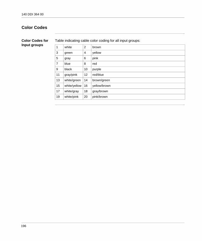
140 DDI 364 00
Color Codes
Color Codes for Input groups
Table indicating cable color coding for all input groups:
1 white 2 brown
3 green 4 yellow
5 gray 6 pink
7 blue 8 red
9 black 10 purple
11 gray/pink 12 red/blue
13 white/green 14 brown/green
15 white/yellow 16 yellow/brown
17 white/gray 18 gray/brown
19 white/pink 20 pink/brown
196

140 DDI 364 00
Specifications
General Specifications
General Specifications
Isolation Isolation
Input Rating Input Rating
Absolute Maximum Inputs
Absolute Maximum Inputs
Response Response
Fuses Fuses
Module Type 96 IN (6 groups x 16 points)
Power Dissipation 1.35 W + 0.13 W x the number of points ON
Bus Current required 270 mA (max.)
I/O map 6 input words
Group to Group 500 VAC rms for 1 minute
Group to Bus -
ON Level voltage +15 VDC
OFF Level voltage +5 VDC
ON Level current 2.5 mA (min.)
OFF Level current 0.7 mA
Internal Resistance 6.7 kohm
Input Protection Resistor Limited
Continuous 30 VDC
1.0 ms 50 VDC
OFF - ON 2.0 ms (max.)
ON - OFF 3.0 ms (max.)
Internal -
External User discretion
197

140 DDI 364 00
Parameter Configuration
Parameter and Default values
Parameter Configuration Window
Name Default Value Options Description
Mapping BIT (%I-1x) WORD (%IW-3X)
Inputs Starting Address 1 1
Inputs Ending Address 96 6
Task(Grayed if module in other than local)
MAST FASTAUX0AUX1AUX2AUX3
fixed to MAST if module in other than local
DC Input 24v DC 6x16 Sink
ConfigParameter Name Value
MAPPING BIT (%I-1X)INPUTS STARTING ADDRESS 1INPUTS ENDING ADDRESS 96TASK MAST
1 : Local Qu... 2 : 140 DDI.
198

17
140 DDI 673 00: 125 VDC 3x8 Sink IN ModuleOverview
Purpose The following chapter provides information of the Quantum 140 DDI 673 00 Module.
What's in this Chapter?
This chapter contains the following topics:
Topic Page
Presentation 200
Indicators 201
Wiring Diagram 202
Specifications 204
Parameter Configuration 207
199

140 DDI 673 00
Presentation
Function The DC Input 125 VDC 3x8 Sink module accepts 125 VDC inputs and is for use with source output devices. The module has software-selectable response time to provide additional input filtering.
Illustration The following figure shows the 140 DDI 673 00 module and its components.
1 Model Number, Module Description, Color Code
2 LED Display
3 Fuse Cutouts
4 Field Wiring Terminal Strip
5 Removable Door
6 Customer Identification Label (Fold label and place it inside door)
Note: The field wiring terminal strip (Modicon #140 XTS 002 00) must be ordered separately. (The terminal strip includes the removable door and label.)
140DDI 673 00
X X
XXXXXXXXXXXXXXXXXXXX
XXXXXXXXXXXXXXXXXXXXX
23
6
8
10
1214
16
18
20
21
232527
29
31
3335
37
1
4
7
9
11
13
1517
19
22
24
26
28
30
32
34
3638
1
2
3
4 5
6
200

140 DDI 673 00
Indicators
Illustration The following table shows the LED indicators for the 140 DDI 673 00 module.
Descriptions The following table shows the LED descriptions for the 140 DDI 673 00 module.
Active
91102113
1245678
13141516
171819
2021222324
LEDs Color Indication when ON
Active Green Bus communication is present.
1 ... 24 Green The indicated point or channel is turned ON.
201

140 DDI 673 00
Wiring Diagram
Illustration The following figure shows the DDI 673 00 wiring diagram.
INPUT 1+ -
INPUT 3
INPUT 5
INPUT 7
GROUP B COMMON
GROUP C COMMON
INPUT9
INPUT 11
INPUT13
INPUT15
INPUT 17
INPUT 19
INPUT 21
INPUT 23
N/C
N/C
N/C
N/C
INPUT 2
INPUT 4
INPUT 6
INPUT 8
INPUT 12
INPUT 14
INPUT 16
INPUT 18
INPUT 20
INPUT 22
INPUT 24
GROUP A COMMON
FIELD DEVICE
N/C
N/C
2
10
4
6
8
12
14
16
18
20
22
24
26
28
30
32
34
36
38
40 39
37
35
33
31
29
27
25
23
21
19
17
15
13
11
9
7
5
3
1
INPUT 10
N/C
N/C
N/C
N/C
N/C
N/C
N/C
202

140 DDI 673 00
Note: N / C = Not Connected
Note: When field wiring the I/O module, the maximum wire size that should be used is 1-14 AWG or 2-16 AWG; the minimum size is 20 AWG.
203
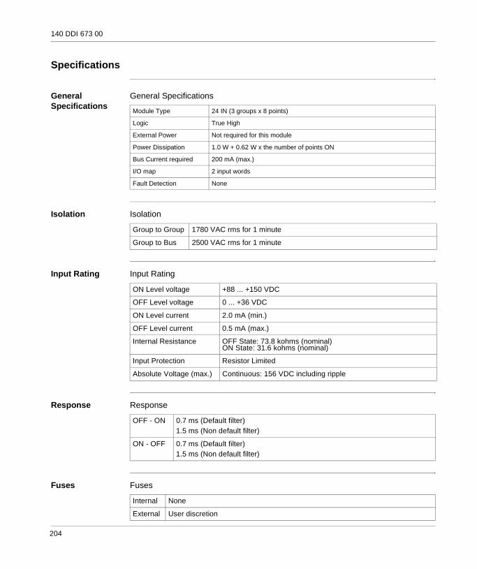
140 DDI 673 00
Specifications
General Specifications
General Specifications
Isolation Isolation
Input Rating Input Rating
Response Response
Fuses Fuses
Module Type 24 IN (3 groups x 8 points)
Logic True High
External Power Not required for this module
Power Dissipation 1.0 W + 0.62 W x the number of points ON
Bus Current required 200 mA (max.)
I/O map 2 input words
Fault Detection None
Group to Group 1780 VAC rms for 1 minute
Group to Bus 2500 VAC rms for 1 minute
ON Level voltage +88 ... +150 VDC
OFF Level voltage 0 ... +36 VDC
ON Level current 2.0 mA (min.)
OFF Level current 0.5 mA (max.)
Internal Resistance OFF State: 73.8 kohms (nominal)ON State: 31.6 kohms (nominal)
Input Protection Resistor Limited
Absolute Voltage (max.) Continuous: 156 VDC including ripple
OFF - ON 0.7 ms (Default filter) 1.5 ms (Non default filter)
ON - OFF 0.7 ms (Default filter) 1.5 ms (Non default filter)
Internal None
External User discretion
204
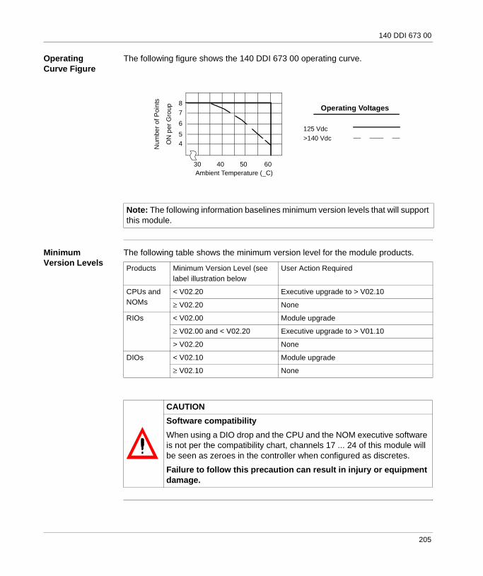
140 DDI 673 00
Operating Curve Figure
The following figure shows the 140 DDI 673 00 operating curve.
Minimum Version Levels
The following table shows the minimum version level for the module products.
Note: The following information baselines minimum version levels that will support this module.
30Ambient Temperature (_C)
Num
ber o
f Poi
nts
ON
per
Gro
up
5678
40 50 60
4
Operating Voltages
125 Vdc>140 Vdc
Products Minimum Version Level (see label illustration below
User Action Required
CPUs and NOMs
< V02.20 Executive upgrade to > V02.10
≥ V02.20 None
RIOs < V02.00 Module upgrade
≥ V02.00 and < V02.20 Executive upgrade to > V01.10
> V02.20 None
DIOs < V02.10 Module upgrade
≥ V02.10 None
CAUTIONSoftware compatibilityWhen using a DIO drop and the CPU and the NOM executive software is not per the compatibility chart, channels 17 ... 24 of this module will be seen as zeroes in the controller when configured as discretes.Failure to follow this precaution can result in injury or equipment damage.
205

140 DDI 673 00
Version Label Figure
The following figure shows the version label.
Note: The version label is found on the top front of the module.
140CPU 424 02Controller
CPU 2M2XMB+ 02.20
206
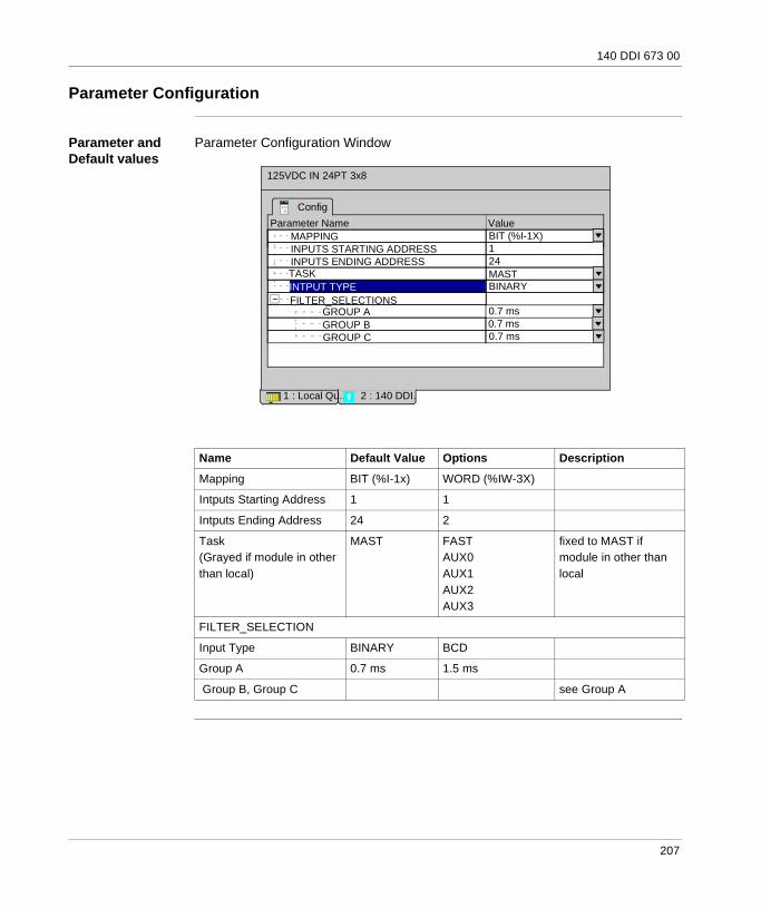
140 DDI 673 00
Parameter Configuration
Parameter and Default values
Parameter Configuration Window
Name Default Value Options Description
Mapping BIT (%I-1x) WORD (%IW-3X)
Intputs Starting Address 1 1
Intputs Ending Address 24 2
Task(Grayed if module in other than local)
MAST FASTAUX0AUX1AUX2AUX3
fixed to MAST if module in other than local
FILTER_SELECTION
Input Type BINARY BCD
Group A 0.7 ms 1.5 ms
Group B, Group C see Group A
125VDC IN 24PT 3x8
ConfigParameter Name Value
MAPPING BIT (%I-1X)INPUTS STARTING ADDRESS 1INPUTS ENDING ADDRESS 24
INTPUT TYPE BINARY
1 : Local Qu... 2 : 140 DDI.
FILTER_SELECTIONS GROUP AGROUP B
TASK MAST
GROUP C0.7 ms0.7 ms
0.7 ms
207

140 DDI 673 00
208

18
140 DDI 841 00: 10 ... 60 VDC 8x2 Sink IN ModuleOverview
Purpose The following chapter provides information of the Quantum 140 DDI 841 00 Module.
What's in this Chapter?
This chapter contains the following topics:
Topic Page
Presentation 210
Indicators 211
Wiring Diagram 212
Specifications 214
Parameter Configuration 216
209

140 DDI 841 00
Presentation
Function The DC Input 10 ... 60 VDC 8x2 Sink module accepts 10 ... 60 VDC inputs and is for use with source output devices. ON-OFF levels are dependent on the reference voltage selected. Different reference voltages may be used for different groups.
Illustration The following figure shows the 140 DDI 841 00 module and its components.
1 Model Number, Module Description, Color Code
2 LED Display
3 Fuse Cutouts
4 Field Wiring Terminal Strip
5 Removable Door
6 Customer Identification Label (Fold label and place it inside door)
Note: The field wiring terminal strip (Modicon #140 XTS 002 00) must be ordered separately. (The terminal strip includes the removable door and label.)
140DDI 841 00
X X
XXXXXXXXXXXXXXXXXXXX
XXXXXXXXXXXXXXXXXXXXX
23
6
8
10
1214
16
18
20
21
232527
29
31
3335
37
1
4
7
9
11
13
1517
19
22
24
26
28
30
32
34
3638
1
2
3
4 5
6
210

140 DDI 841 00
Indicators
Illustration The following table shows the LED indicators for the 140 DDI 841 00 module.
Descriptions The following table shows the LED descriptions for the 140 DDI 841 00 module.
Active
91102113
1245678
13141516
123
45678
91011
1213141516
LEDs Color Indication when ON
Active Green Bus communication is present.
1 ... 16 Green The indicated point or channel is turned ON.
1 ... 16 Red There is a fault on the indicated point or channel.
211

140 DDI 841 00
Wiring Diagram
Illustration The following figure shows the 140 DDI 841 00 wiring diagram.
INPUT 1+ -
INPUT 3
INPUT 7
INPUT 9
INPUT 13
INPUT 15
N/C
N/C
N/C
INPUT 2
GROUP A SUPPLY
INPUT 4
INPUT 10
INPUT 14
INPUT 16
FIELD DEVICE
INPUT 8
N/C
N/C
GROUP B SUPPLY
GROUP D SUPPLY
GROUP E SUPPLY
INPUT 12
GROUP F SUPPLY
N/C
GROUP G SUPPLY
GROUP H SUPPLY
INPUT 6
GROUP C SUPPLY
GROUP A COMMON
GROUP B COMMON
INPUT 5
GROUP C COMMON
GROUP D COMMON
N/C
GROUP E COMMON
INPUT 11
GROUP F COMMON
GROUP G COMMON
GROUP H COMMON
N/C
2
10
4
6
8
12
14
16
18
20
22
24
26
28
30
32
34
36
38
40 39
37
35
33
31
29
27
25
23
21
19
17
15
13
11
9
7
5
3
1
212

140 DDI 841 00
Note: N / C = Not Connected
Note: When field wiring the I/O module, the maximum wire size that should be used is 1-14 AWG or 2-16 AWG; the minimum size is 20 AWG.
213

140 DDI 841 00
Specifications
General Specifications
General Specifications
Group Supply / Tolerance
Group Supply / Tolerance
Isolation Isolation
Fuses Fuses
Input Rating Input Rating
Module Type 16 IN (8 groups x 2 points)
Logic True High
External Power 10 ... 60 VDC (group supply)
Power Dissipation 1.0 W + 0.25 W x the number of points ON
Bus Current required 200 mA
I/O map 1 input word
Group supply / Tolerance ON* State OFF* State
12 VDC / +/-5% 9 ... 12 0 ... 1.8 IEC 57 Class2
24 VDC / -15% ... +20% 11 ... 24 0 ... 5 IEC 65A Typ2
48 VDC / -15% ... +20% 34 ... 48 0 ... 10 IEC 65A Typ2
60 VDC / -15% ... +20% 45 ... 60 0 ... 9 IEC 57 Class1*ON / OFF state ranges are specified at nominal reference voltages.
Group to Group 700 VAC rms for 1 minute
Group to Bus 2500 VAC rms for 1 minute
Internal None
External User discretion
Absolute Maximum Input 75 VDC
Input Protection Resistor Limited
214

140 DDI 841 00
ON State Current ON State Current
Response / Switching Frequency
Response / Switching Frequency
@ 12 VDC 5 ... 10 mA
@ 24 VDC 6 ... 30 mA
@ 48 VDC 2 ... 15 mA
@ 60 VDC 1 ... 5 mA
OFF - ON 4 ms
ON - OFF 4 ms
Switching Frequency < 100 Hz
215

140 DDI 841 00
Parameter Configuration
Parameter and Default values
Parameter Configuration Window
Name Default Value Options Description
Mapping BIT (%I-1x) WORD (%IW-3X)
Inputs Starting Address 1 1
Inputs Ending Address 16 1
Input Type BINARY BCD
Task(Grayed if module in other than local)
MAST FASTAUX0AUX1AUX2AUX3
fixed to MAST if module in other than local
DC IN 10-60V 8x2
ConfigParameter Name Value
MAPPING BIT (%I-1X)INPUTS STARTING ADDRESS 1INPUTS ENDING ADDRESS 16INPUT TYPE BINARY
1 : Local Qu... 2 : 140 DDI.
TASK MAST
216

19
140 DDI 853 00: 10 ... 60 VDC 4x8 Sink IN ModuleOverview
Purpose The following chapter provides information of the Quantum 140 DDI 853 00 Module.
What's in this Chapter?
This chapter contains the following topics:
Topic Page
Presentation 218
Indicators 219
Wiring Diagram 220
Specifications 222
Parameter Configuration 224
217

140 DDI 853 00
Presentation
Function The DC Input 10 ... 60 VDC 4x8 Sink module accepts 10 ... 60 VDC inputs and is for use with source output devices. ON-OFF levels are dependent on the reference voltage selected. Different reference voltages may be used for different groups.
Illustration The following figure shows the 140 DDI 853 00 module and its components.
1 Model Number, Module Description, Color Code
2 LED Display
3 Fuse Cutouts
4 Field Wiring Terminal Strip
5 Removable Door
6 Customer Identification Label (Fold label and place it inside door)
Note: The field wiring terminal strip (Modicon #140 XTS 002 00) must be ordered separately. (The terminal strip includes the removable door and label.)
140DDI 853 00
X X
XXXXXXXXXXXXXXXXXXXX
XXXXXXXXXXXXXXXXXXXXX
23
6
8
10
1214
16
18
20
21
232527
29
31
3335
37
1
4
7
9
11
13
1517
19
22
24
26
28
30
32
34
3638
1
2
3
4 5
6
218

140 DDI 853 00
Indicators
Illustration The following table shows the LED indicators for the 140 DDI 853 00 module.
Descriptions The following table shows the LED descriptions for the 140 DDI 853 00 module.
Active
91102113
1245678
13141516
171819
2021222324
252627
2829303132
LEDs Color Indication when ON
Active Green Bus communication is present.
1 ... 32 Green The indicated point or channel is turned ON.
219

140 DDI 853 00
Wiring Diagram
Illustration The following figure shows the 140 DDI 853 00 wiring diagram.
INPUT 1+ -
INPUT 25
INPUT 29
INPUT 2
INPUT 26
INPUT 30
FIELD DEVICE
INPUT 22
INPUT 10
INPUT 21
INPUT 4
INPUT 6
INPUT 8
GROUP A SUPPLY
INPUT 12
INPUT 14
INPUT 16
GROUP B SUPPLY
INPUT 18
INPUT 20
INPUT 24
GROUP C SUPPLY
INPUT 28
INPUT 32
GROUP D SUPPLY
2
10
4
6
8
12
14
16
18
20
22
24
26
28
30
32
34
36
38
40 39
37
35
33
31
29
27
25
23
21
19
17
15
13
11
9
7
5
3
1
INPUT3
INPUT5
INPUT 7
GROUP A COMMON
INPUT 9
INPUT 11
INPUT 13
INPUT 15
GROUP B COMMON
INPUT 17
INPUT 19
INPUT 23
GROUP C COMMON
INPUT 27
INPUT 31
GROUP D COMMON
220

140 DDI 853 00
Note: When field wiring the I/O module, the maximum wire size that should be used is 1-14 AWG or 2-16 AWG; the minimum size is 20 AWG.
221
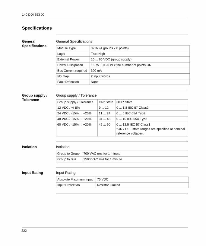
140 DDI 853 00
Specifications
General Specifications
General Specifications
Group supply / Tolerance
Group supply / Tolerance
Isolation Isolation
Input Rating Input Rating
Module Type 32 IN (4 groups x 8 points)
Logic True High
External Power 10 ... 60 VDC (group supply)
Power Dissipation 1.0 W + 0.25 W x the number of points ON
Bus Current required 300 mA
I/O map 2 input words
Fault Detection None
Group supply / Tolerance ON* State OFF* State
12 VDC / +/-5% 9 ... 12 0 ... 1.8 IEC 57 Class2
24 VDC / -15% ... +20% 11 ... 24 0 ... 5 IEC 65A Typ2
48 VDC / -15% ... +20% 34 ... 48 0 ... 10 IEC 65A Typ2
60 VDC / -15% ... +20% 45 ... 60 0 ... 12.5 IEC 57 Class1*ON / OFF state ranges are specified at nominal reference voltages.
Group to Group 700 VAC rms for 1 minute
Group to Bus 2500 VAC rms for 1 minute
Absolute Maximum Input 75 VDC
Input Protection Resistor Limited
222

140 DDI 853 00
ON State Current ON State Current
Response / Switching Frequency
Response / Switching Frequency
Fuses Fuses
@ 12 VDC 5 ... 10 mA
@ 24 VDC 6 ... 30 mA
@ 48 VDC 2 ... 15 mA
@ 60 VDC 1 ... 5 mA
OFF - ON 4 ms
ON - OFF 4 ms
Switching Frequency < 100 Hz max.
Internal None
External User discretion
223

140 DDI 853 00
Parameter Configuration
Parameter and Default values
Parameter Configuration Window
Name Default Value Options Description
Mapping BIT (%I-1x) WORD (%IW-3X)
Inputs Starting Address 1 1
Inputs Ending Address 32 2
Input Type BINARY BCD
Task(Grayed if module in other than local)
MAST FASTAUX0AUX1AUX2AUX3
fixed to MAST if module in other than local
DC IN 10-60V 4x8
ConfigParameter Name Value
MAPPING BIT (%I-1X)INPUTS STARTING ADDRESS 1INPUTS ENDING ADDRESS 32INPUT TYPE BINARY
1 : Local Qu... 2 : 140 DDI.
TASK MAST
224

20
140 DAI 340 00: 24 VAC 16x1 IN ModuleOverview
Purpose The following chapter provides information of the Quantum 140 DAI 340 00 Module.
What's in this Chapter?
This chapter contains the following topics:
Topic Page
Presentation 226
Indicators 227
Wiring Diagram 228
Specifications 230
Parameter Configuration 232
225

140 DAI 340 00
Presentation
Function The AC Input 24 VAC 16x1 module accepts 24 VAC inputs.
Illustration The following figure shows the 140 DAI 340 00 module and its components.
1 Model Number, Module Description, Color Code
2 LED Display
3 Fuse Cutouts
4 Field Wiring Terminal Strip
5 Removable Door
6 Customer Identification Label (Fold label and place it inside door)
Note: The field wiring terminal strip (Modicon #140 XTS 002 00) must be ordered separately. (The terminal strip includes the removable door and label.)
140DAI 340 00
X X
XXXXXXXXXXXXXXXXXXXX
XXXXXXXXXXXXXXXXXXXXX
23
6
8
10
1214
16
18
20
21
232527
29
31
3335
37
1
4
7
9
11
13
1517
19
22
24
26
28
30
32
34
3638
1
2
3
4 5
6
226
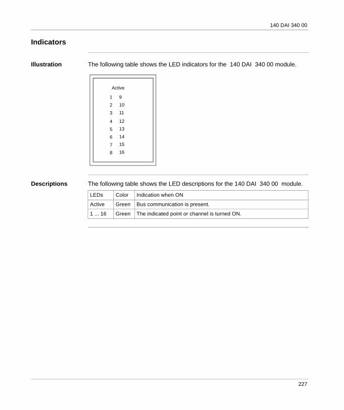
140 DAI 340 00
Indicators
Illustration The following table shows the LED indicators for the 140 DAI 340 00 module.
Descriptions The following table shows the LED descriptions for the 140 DAI 340 00 module.
Active
91102113
1245678
13141516
LEDs Color Indication when ON
Active Green Bus communication is present.
1 ... 16 Green The indicated point or channel is turned ON.
227

140 DAI 340 00
Wiring Diagram
Illustration The following figure shows the 140 DAI 340 00 wiring diagram.
RETURN 1 INPUT 12
10
4
6
8
12
14
16
18
20
22
24
26
28
30
32
34
36
38
40 39
37
35
33
31
29
27
25
23
21
19
17
15
13
11
9
7
5
3
1RETURN 2
RETURN 3
RETURN 4
RETURN 5
RETURN 6
RETURN 7
RETURN 8
RETURN 9
RETURN 10
RETURN 11
RETURN 12
RETURN 13
RETURN 14
RETURN 15
RETURN 16
INPUT 2
INPUT 3
INPUT 4
INPUT 5
INPUT 6
INPUT 7
INPUT 8
INPUT 9
INPUT 10
INPUT 11
INPUT 12
INPUT 13
INPUT 14
INPUT 15
INPUT 16
N/C N/C
N/C
N/C
N/C
N/C
N/C
N/C
L N
228

140 DAI 340 00
Note: This module is not polarity sensitive.N / C = Not Connected.
Note: When field wiring the I/O module, the maximum wire size that should be used is 1-14 AWG or 2-16 AWG; the minimum size is 20 AWG.
229

140 DAI 340 00
Specifications
General Specifications
General Specifications
Operating Voltage and Input Current*
Operating Voltage and Input Current*
Typical Input Impedance
Typical Imput Impedance
Isolation Isolation
Module Type 16 IN (16 groups x 1 point) individually isolated
External Power Not required for this module
Power Dissipation 5.5 W (max.)
Bus Current required 180 mA
I/O map 1 input word
Fault Detection None
50 Hz ON: 14 ... 30 VAC (11.1 mA max.)OFF: 0 ... 5 VAC
60 Hz ON: 12 ... 30 VAC (13.2 mA max.) OFF: 0 ... 5 VAC* Do not use outside the 47 ... 63 Hz range
Maximum Allowable Leakage Current from an External Device to be recognized as an OFF Condition.
1.9 mA
50 Hz 3.1 kohms capacitive
60 Hz 2.6 kohms
Input to Input 1780 VAC for 1 minute
Input to Bus 1780 VAC for 1 minute
230

140 DAI 340 00
Absolute Maximum Input
Absolute Maximum Input
Response Response
Fuses Fuses
Continuous 30 VAC
10 s 32 VAC
1 Cycle 50 VAC
OFF - ON Min: 4.9 ms. Max: 0.75 line cycle.
ON - OFF Min: 7.3 ms. Max: 12.3 ms.
Internal None
External User discretion
231

140 DAI 340 00
Parameter Configuration
Parameter and Default values
Parameter Configuration Window
Name Default Value Options Description
Mapping BIT (%I-1x) WORD (%IW-3X)
Inputs Starting Address 1 1
Inputs Ending Address 16 1
Input Type BINARY BCD
Task(Grayed if module in other than local)
MAST FASTAUX0AUX1AUX2AUX3
fixed to MAST if module in other than local
AC IN 24V 2x8
ConfigParameter Name Value
MAPPING BIT (%I-1X)INPUTS STARTING ADDRESS 1INPUTS ENDING ADDRESS 16INPUT TYPE BINARY
1 : Local Qu... 2 : 140 DAI.
TASK MAST
232

21
140 DAI 353 00: 24 VAC 4x8 IN ModuleOverview
Purpose The following chapter provides information of the Quantum 140 DAI 353 00 Module.
What's in this Chapter?
This chapter contains the following topics:
Topic Page
Presentation 234
Indicators 235
Wiring Diagram 236
Specifications 238
Parameter Configuration 240
233

140 DAI 353 00
Presentation
Function The AC Input 24 VAC 4x8 module accepts 24 VAC inputs.
Illustration The following figure shows the 140 DAI 353 00 module and its components.
1 Model Number, Module Description, Color Code
2 LED Display
3 Fuse Cutouts
4 Field Wiring Terminal Strip
5 Removable Door
6 Customer Identification Label (Fold label and place it inside door)
Note: The field wiring terminal strip (Modicon #140 XTS 002 00) must be ordered separately. (The terminal strip includes the removable door and label.)
140DAI 353 00
X X
XXXXXXXXXXXXXXXXXXXX
XXXXXXXXXXXXXXXXXXXXX
23
6
8
10
1214
16
18
20
21
232527
29
31
3335
37
1
4
7
9
11
13
1517
19
22
24
26
28
30
32
34
3638
1
2
3
4 5
6
234

140 DAI 353 00
Indicators
Illustration The following table shows the LED indicators for the 140 DAI 353 00 module.
Descriptions The following table shows the LED descriptions for the 140 DAI 353 00 module.
Active F
91102113
1245678
13141516
171819
2021222324
252627
2829303132
LEDs Color Indication when ON
Active Green Bus communication is present.
F Red A fault (external to the module) has been detected.
1 ... 32 Green The indicated point or channel is turned ON.
235

140 DAI 353 00
Wiring Diagram
Illustration The following figure shows the 140 DAI 353 00 wiring diagram. INPUT 1
2
10
4
6
8
12
14
16
18
20
22
24
26
28
30
32
34
36
38
40 39
37
35
33
31
29
27
25
23
21
19
17
15
13
11
9
7
5
3
1L NINPUT 2
INPUT 4
INPUT 6
INPUT 8
N/C
INPUT 10
INPUT 12
INPUT 14
INPUT 16
INPUT 18
INPUT 20
INPUT 22
INPUT 24
INPUT 26
INPUT 28
INPUT 30
INPUT 32
N/C
N/C
N/C
INPUT 3
INPUT 5
INPUT 7
GROUP A COMMON
GROUP B COMMON
GROUP C COMMON
GROUP D COMMON
INPUT 9
INPUT 11
INPUT 13
INPUT 15
INPUT 17
INPUT 19
INPUT 21
INPUT 23
INPUT 25
INPUT 27
INPUT 29
INPUT 31
236

140 DAI 353 00
Note: This module is not polarity sensitive.N / C = Not Connected.
Note: When field wiring the I/O module, the maximum wire size that should be used is 1-14 AWG or 2-16 AWG; the minimum size is 20 AWG.
237

140 DAI 353 00
Specifications
General Specifications
General Specifications
Operating Voltage and Input Current*
Operating Voltage and Input Current*
Typical Input Impedance
Typical Imput Impedance
Isolation Isolation
Fuses Fuses
Module Type 32 IN (4 groups x 8 points)
External Power Not required for this module
Power Dissipation 10.9 W (max.)
Bus Current required 250 mA
I/O map 2 input words
Fault Detection None
50 Hz ON: 14 ... 30 VAC (11.1 mA max)OFF: 0 ... 5 VAC
60 Hz ON: 12 ... 30 VAC (13.2 mA max) OFF: 0 ... 5 VAC* Do not use outside the 47 ... 63 Hz range
Maximum Allowable Leakage Current from an External Device to be recognized as an OFF Condition.
1.9 mA
50 Hz 3.1 kohms capacitive
60 Hz 2.6 kohms capacitive
Group to Group 1780 VAC for 1 minute
Input to Bus 1780 VAC for 1 minute
Internal None
External User discretion
238

140 DAI 353 00
Absolute Maximum Input
Absolute Maximum Input
Response Response
Continuous 30 VAC
10 s 32 VAC
1 Cycle 50 VAC
OFF - ON Min: 4.9 ms. Max: 0.75 line cycle.
ON - OFF Min: 7.3 ms. Max: 12.3 ms.
Note: Input signals must be sinusoidal with less than 6% THD and 63 Hz maximum frequency.
239
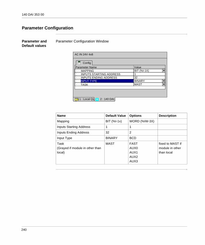
140 DAI 353 00
Parameter Configuration
Parameter and Default values
Parameter Configuration Window
Name Default Value Options Description
Mapping BIT (%I-1x) WORD (%IW-3X)
Inputs Starting Address 1 1
Inputs Ending Address 32 2
Input Type BINARY BCD
Task(Grayed if module in other than local)
MAST FASTAUX0AUX1AUX2AUX3
fixed to MAST if module in other than local
AC IN 24V 4x8
ConfigParameter Name Value
MAPPING BIT (%I-1X)INPUTS STARTING ADDRESS 1INPUTS ENDING ADDRESS 32INPUT TYPE BINARY
1 : Local Qu... 2 : 140 DAI.
TASK MAST
240

22
140 DAI 440 00: 48 VAC 16x1 IN ModuleOverview
Purpose The following chapter provides information of the Quantum 140 DAI 440 00 Module.
What's in this Chapter?
This chapter contains the following topics:
Topic Page
Presentation 242
Indicators 243
Wiring Diagram 244
Specifications 246
Parameter Configuration 248
241

140 DAI 440 00
Presentation
Function The AC Input 48 VAC 16x1 module accepts 48 VAC inputs.
Illustration The following figure shows the 140 DAI 440 00 module and its components.
1 Model Number, Module Description, Color Code
2 LED Display
3 Fuse Cutouts
4 Field Wiring Terminal Strip
5 Removable Door
6 Customer Identification Label (Fold label and place it inside door)
Note: The field wiring terminal strip (Modicon #140 XTS 002 00) must be ordered separately. (The terminal strip includes the removable door and label.)
140DAI 440 00
X X
XXXXXXXXXXXXXXXXXXXX
XXXXXXXXXXXXXXXXXXXXX
23
6
8
10
1214
16
18
20
21
232527
29
31
3335
37
1
4
7
9
11
13
1517
19
22
24
26
28
30
32
34
3638
1
2
3
4 5
6
242

140 DAI 440 00
Indicators
Illustration The following table shows the LED indicators for the 140 DAI 440 00 module.
Descriptions The following table shows the LED descriptions for the 140 DAI 440 00 module.
Active
91102113
1245678
13141516
LEDs Color Indication when ON
Active Green Bus communication is present.
1 ... 16 Green The indicated point or channel is turned ON.
243

140 DAI 440 00
Wiring Diagram
Illustration The following figure shows the 140 DAI 440 00 wiring diagram.
RETURN 1 INPUT 12
10
4
6
8
12
14
16
18
20
22
24
26
28
30
32
34
36
38
40 39
37
35
33
31
29
27
25
23
21
19
17
15
13
11
9
7
5
3
1RETURN 2
RETURN 3
RETURN 4
RETURN 5
RETURN 6
RETURN 7
RETURN 8
RETURN 9
RETURN 10
RETURN 11
RETURN 12
RETURN 13
RETURN 14
RETURN 15
RETURN 16
INPUT 2
INPUT 3
INPUT 4
INPUT 5
INPUT 6
INPUT 7
INPUT 8
INPUT 9
INPUT 10
INPUT 11
INPUT 12
INPUT 13
INPUT 14
INPUT 15
INPUT 16
N/C N/C
N/C
N/C
N/C
N/C
N/C
N/C
L N
244

140 DAI 440 00
Note: This module is not polarity sensitive.N / C = Not Connected
Note: When field wiring the I/O module, the maximum wire size that should be used is 1-14 AWG or 2-16 AWG; the minimum size is 20 AWG.
245

140 DAI 440 00
Specifications
General Specifications
General Specifications
Operating Voltage and Input Current*
Operating Voltage and Input Current*
Typical Input Impedance
Typical Imput Impedance
Isolation Isolation
Module Type 16 individually isolated
External Power Not required for this module
Power Dissipation 5.5 W (max.)
Bus Current required 180 mA
I/O map 1 input word
Fault Detection None
50 Hz ON: 34 ... 56 VAC (9.8 mA max)OFF: 0 ... 10 VAC
60 Hz ON: 29 ... 56 VAC (11.7 mA max) OFF: 0 ... 10 VAC* Do not use outside the 47 ... 63 Hz range
Maximum Allowable Leakage Current from an External Device to be recognized as an OFF Condition.
1.7 mA
50 Hz 6.8 kohms capacitive
60 Hz 5.6 kohms capacitive
Group to Group 1780 VAC for 1 minute
Input to Bus 1780 VAC for 1 minute
246
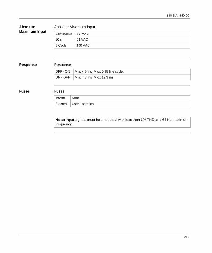
140 DAI 440 00
Absolute Maximum Input
Absolute Maximum Input
Response Response
Fuses Fuses
Continuous 56 VAC
10 s 63 VAC
1 Cycle 100 VAC
OFF - ON Min: 4.9 ms. Max: 0.75 line cycle.
ON - OFF Min: 7.3 ms. Max: 12.3 ms.
Internal None
External User discretion
Note: Input signals must be sinusoidal with less than 6% THD and 63 Hz maximum frequency.
247

140 DAI 440 00
Parameter Configuration
Parameter and Default values
Parameter Configuration Window
Name Default Value Options Description
Mapping BIT (%I-1x) WORD (%IW-3X)
Inputs Starting Address 1 1
Inputs Ending Address 16 1
Input Type BINARY BCD
Task(Grayed if module in other than local)
MAST FASTAUX0AUX1AUX2AUX3
fixed to MAST if module in other than local
AC IN 48V 2x8
ConfigParameter Name Value
MAPPING BIT (%I-1X)INPUTS STARTING ADDRESS 1INPUTS ENDING ADDRESS 16INPUT TYPE BINARY
1 : Local Qu... 2 : 140 DAI.
TASK MAST
248

23
140 DAI 453 00: 48 VAC 4x8 IN ModuleOverview
Purpose The following chapter provides information of the Quantum 140 DAI 453 00 Module.
What's in this Chapter?
This chapter contains the following topics:
Topic Page
Presentation 250
Indicators 251
Wiring Diagram 252
Specifications 254
Parameter Configuration 256
249

140 DAI 453 00
Presentation
Function The AC Input 48 VAC 4x8 module accepts 48 VAC inputs.
Illustration The following figure shows the 140 DAI 453 00 module and its components.
1 Model Number, Module Description, Color Code
2 LED Display
3 Fuse Cutouts
4 Field Wiring Terminal Strip
5 Removable Door
6 Customer Identification Label (Fold label and place it inside door)
Note: The field wiring terminal strip (Modicon #140 XTS 002 00) must be ordered separately. (The terminal strip includes the removable door and label.)
140DAI 453 00
X X
XXXXXXXXXXXXXXXXXXXX
XXXXXXXXXXXXXXXXXXXXX
23
6
8
10
1214
16
18
20
21
232527
29
31
3335
37
1
4
7
9
11
13
1517
19
22
24
26
28
30
32
34
3638
1
2
3
4 5
6
250

140 DAI 453 00
Indicators
Illustration The following table shows the LED indicators for the 140 DAI 453 00 module.
Descriptions The following table shows the LED descriptions for the 140 DAI 453 00 module.
Active F
91102113
1245678
13141516
171819
2021222324
252627
2829303132
LEDs Color Indication when ON
Active Green Bus communication is present.
F Red A fault (external to the module) has been detected.
1 ... 32 Green The indicated point or channel is turned ON.
251

140 DAI 453 00
Wiring Diagram
Illustration The following figure shows the 140 DAI 453 00 wiring diagram.
INPUT 12
10
4
6
8
12
14
16
18
20
22
24
26
28
30
32
34
36
38
40 39
37
35
33
31
29
27
25
23
21
19
17
15
13
11
9
7
5
3
1L NINPUT 2
INPUT 4
INPUT 6
INPUT 8
N/C
INPUT 10
INPUT 12
INPUT 14
INPUT 16
INPUT 18
INPUT 20
INPUT 22
INPUT 24
INPUT 26
INPUT 28
INPUT 30
INPUT 32
N/C
N/C
N/C
INPUT 3
INPUT 5
INPUT 7
GROUP A COMMON
GROUP B COMMON
GROUP C COMMON
GROUP D COMMON
INPUT 9
INPUT 11
INPUT 13
INPUT 15
INPUT 17
INPUT 19
INPUT 21
INPUT 23
INPUT 25
INPUT 27
INPUT 29
INPUT 31
252

140 DAI 453 00
Note: This module is not polarity sensitive.N / C = Not Connected.
Note: When field wiring the I/O module, the maximum wire size that should be used is 1-14 AWG or 2-16 AWG; the minimum size is 20 AWG.
253

140 DAI 453 00
Specifications
General Specifications
General Specifications
Operating Voltage and Input Current*
Operating Voltage and Input Current*
Typical Input Impedance
Typical Imput Impedance
Isolation Isolation
Absolute Maximum Input
Absolute Maximum Input
Module Type 32 IN (4 groups x 8 points)
External Power Not required for this module
Power Dissipation 10.9 W (max.)
Bus Current required 250 mA
I/O map 2 input words
Fault Detection None
50 Hz ON: 34 ... 56 VAC (9.8 mA max)OFF: 0 ... 10 VAC
60 Hz ON: 29 ... 56 VAC (11.7 mA max) OFF: 0 ... 10 VAC* Do not use outside the 47 ... 63 Hz range
Maximum Allowable Leakage Current from an External Device to be recognized as an OFF Condition.
1.7 mA
50 Hz 6.8 kohms capacitive
60 Hz 5.6 kohms capacitive
Group to Group 1780 VAC for 1 minute
Input to Bus 1780 VAC for 1 minute
Continuous 56 VAC
10 s 63 VAC
1 Cycle 100 VAC
254

140 DAI 453 00
Response Response
Fuses Fuses
OFF - ON Min: 4.9 ms. Max: 0.75 line cycle.
ON - OFF Min: 7.3 ms. Max: 12.3 ms.
Internal None
External User discretion
Note: Input signals must be sinusoidal with less than 6% THD and 63 Hz maximum frequency.
255

140 DAI 453 00
Parameter Configuration
Parameter and Default values
Parameter Configuration Window
Name Default Value Options Description
Mapping BIT (%I-1x) WORD (%IW-3X)
Inputs Starting Address 1 1
Inputs Ending Address 32 2
Input Type BINARY BCD
Task(Grayed if module in other than local)
MAST FASTAUX0AUX1AUX2AUX3
fixed to MAST if module in other than local
AC IN 48V 4x8
ConfigParameter Name Value
MAPPING BIT (%I-1X)INPUTS STARTING ADDRESS 1INPUTS ENDING ADDRESS 32INPUT TYPE BINARY
1 : Local Qu... 2 : 140 DAI.
TASK MAST
256

24
140 DAI 540 00: 115 VAC 16x1 IN ModuleOverview
Purpose The following chapter provides information of the Quantum 140 DAI 540 00 Module.
What's in this Chapter?
This chapter contains the following topics:
Topic Page
Presentation 258
Indicators 259
Wiring Diagram 260
Specifications 262
Parameter Configuration 264
257

140 DAI 540 00
Presentation
Function The AC Input 115 VAC 16x1 module accepts 115 VAC inputs.
Illustration The following figure shows the 140 DAI 540 00 module and its components.
1 Model Number, Module Description, Color Code
2 LED Display
3 Fuse Cutouts
4 Field Wiring Terminal Strip
5 Removable Door
6 Customer Identification Label (Fold label and place it inside door)
Note: The field wiring terminal strip (Modicon #140 XTS 002 00) must be ordered separately. (The terminal strip includes the removable door and label.)
140DAI 540 00
X X
XXXXXXXXXXXXXXXXXXXX
XXXXXXXXXXXXXXXXXXXXX
23
6
8
10
1214
16
18
20
21
232527
29
31
3335
37
1
4
7
9
11
13
1517
19
22
24
26
28
30
32
34
3638
1
2
3
4 5
6
258

140 DAI 540 00
Indicators
Illustration The following table shows the LED indicators for the 140 DAI 540 00 module.
Descriptions The following table shows the LED descriptions for the 140 DAI 540 00 module.
Active
91102113
1245678
13141516
LEDs Color Indication when ON
Active Green Bus communication is present.
1 ... 16 Green The indicated point or channel is turned ON.
259

140 DAI 540 00
Wiring Diagram
Illustration The following figure shows the 140 DAI 540 00 wiring diagram.
RETURN 1 INPUT 12
10
4
6
8
12
14
16
18
20
22
24
26
28
30
32
34
36
38
40 39
37
35
33
31
29
27
25
23
21
19
17
15
13
11
9
7
5
3
1RETURN 2
RETURN 3
RETURN 4
RETURN 5
RETURN 6
RETURN 7
RETURN 8
RETURN 9
RETURN 10
RETURN 11
RETURN 12
RETURN 13
RETURN 14
RETURN 15
RETURN 16
INPUT 2
INPUT 3
INPUT 4
INPUT 5
INPUT 6
INPUT 7
INPUT 8
INPUT 9
INPUT 10
INPUT 11
INPUT 12
INPUT 13
INPUT 14
INPUT 15
INPUT 16
N/C N/C
N/C
N/C
N/C
N/C
N/C
N/C
L N
260

140 DAI 540 00
Note: This module is not polarity sensitive.N / C = Not Connected.
Note: When field wiring the I/O module, the maximum wire size that should be used is 1-14 AWG or 2-16 AWG; the minimum size is 20 AWG.
CAUTIONVoltage CompatibilityAll inputs in a group must be from the same phase of line input voltage.Failure to follow this precaution can result in injury or equipment damage.
261

140 DAI 540 00
Specifications
General Specifications
General Specifications
Operating Voltage and Input Current*
Operating Voltage and Input Current*
Typical Input Impedance
Typical Imput Impedance
Isolation Isolation
Absolute Maximum Input
Absolute Maximum Input
Module Type 16 IN (16 groups x 1 point)
External Power Not required for this module
Power Dissipation 5.5 W (max.)
Bus Current required 180 mA
I/O map 1 input word
Fault Detection None
50 Hz ON: 85 ... 132 VAC (11.1 mA max)OFF: 0 ... 20 VAC
60 Hz ON: 79 ... 132 VAC (13.2 mA max) OFF: 0 ... 20 VAC* Do not use outside the 47 ... 63 Hz range
Maximum Allowable Leakage Current from an External Device to be recognized as an OFF Condition.
2.1 mA
50 Hz 14.4 kohms capacitive
60 Hz 12 kohms capacitive
Input to Input 1780 VAC for 1 minute
Input to Bus 1780 VAC for 1 minute
Continuous 132 VAC
10 s 156 VAC
1 Cycle 200 VAC
262

140 DAI 540 00
Response Response
Fuses Fuses
OFF - ON Min: 4.9 ms. Max: 0.75 line cycle.
ON - OFF Min: 7.3 ms. Max: 12.3 ms.
Internal None
External User discretion
Note: Input signals must be sinusoidal with less than 6% THD and 63 Hz maximum frequency.
263

140 DAI 540 00
Parameter Configuration
Parameter and Default values
Parameter Configuration Window
Name Default Value Options Description
Mapping BIT (%I-1x) WORD (%IW-3X)
Inputs Starting Address 1 1
Inputs Ending Address 16 1
Input Type BINARY BCD
Task(Grayed if module in other than local)
MAST FASTAUX1AUX2AUX3
fixed to MAST if module in other than local
AC IN 115V 16x1
ConfigParameter Name Value
MAPPING BIT (%I-1X)INPUTS STARTING ADDRESS 1INPUTS ENDING ADDRESS 16INPUT TYPE BINARY
1 : Local Qu... 2 : 140 DAI.
TASK MAST
264

25
140 DAI 543 00: 115 VAC 2x8 IN ModuleOverview
Purpose The following chapter provides information of the Quantum 140 DAI 543 00 Module.
What's in this Chapter?
This chapter contains the following topics:
Topic Page
Presentation 266
Indicators 267
Wiring Diagram 268
Specifications 270
Parameter Configuration 272
265

140 DAI 543 00
Presentation
Function The AC Input 115 VAC 2x8 module accepts 115 VAC inputs.
Illustration The following figure shows the 140 DAI 543 00 module and its components.
1 Model Number, Module Description, Color Code
2 LED Display
3 Fuse Cutouts
4 Field Wiring Terminal Strip
5 Removable Door
6 Customer Identification Label (Fold label and place it inside door)
Note: The field wiring terminal strip (Modicon #140 XTS 002 00) must be ordered separately. (The terminal strip includes the removable door and label.)
140DAI 543 00
X X
XXXXXXXXXXXXXXXXXXXX
XXXXXXXXXXXXXXXXXXXXX
23
6
8
10
1214
16
18
20
21
232527
29
31
3335
37
1
4
7
9
11
13
1517
19
22
24
26
28
30
32
34
3638
1
2
3
4 5
6
266

140 DAI 543 00
Indicators
Illustration The following table shows the LED indicators for the 140 DAI 543 00 module.
Descriptions The following table shows the LED descriptions for the 140 DAI 543 00 module.
Active
91102113
1245678
13141516
LEDs Color Indication when ON
Active Green Bus communication is present.
1 ... 16 Green The indicated point or channel is turned ON.
267

140 DAI 543 00
Wiring Diagram
Illustration The following figure shows the 140 DAI 543 00 wiring diagram.
INPUT 12
10
4
6
8
12
14
16
18
20
22
24
26
28
30
32
34
36
38
40 39
37
35
33
31
29
27
25
23
21
19
17
15
13
11
9
7
5
3
1L N
N/C
INPUT 2
INPUT 3
INPUT 4
GROUP A COMMON
GROUP B COMMON
INPUT 5
INPUT 6
INPUT 7
INPUT 8
INPUT 9
INPUT 10
INPUT 11
INPUT 12
INPUT 13
INPUT 14
INPUT 15
INPUT 16
N/C
N/C
N/C
N/C
N/C
N/C
N/C
N/C
N/C
N/C
N/C
N/C
N/C
N/C
N/C
N/C
N/C
N/C
N/C
N/C
N/C
268
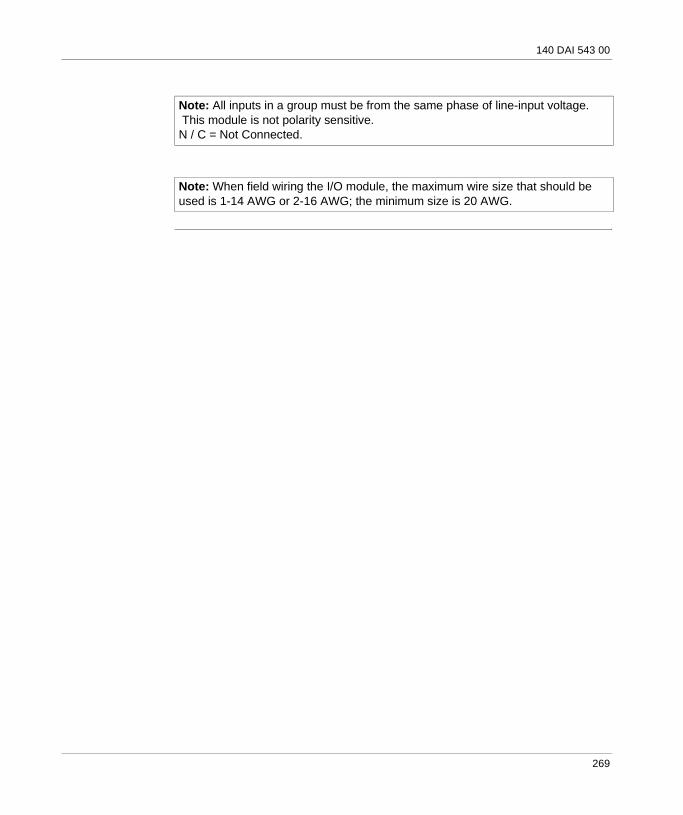
140 DAI 543 00
Note: All inputs in a group must be from the same phase of line-input voltage. This module is not polarity sensitive.N / C = Not Connected.
Note: When field wiring the I/O module, the maximum wire size that should be used is 1-14 AWG or 2-16 AWG; the minimum size is 20 AWG.
269

140 DAI 543 00
Specifications
General Specifications
General Specifications
Operating Voltage and Input Current*
Operating Voltage and Input Current*
Typical Input Impedance
Typical Imput Impedance
Isolation Isolation
Absolute Maximum Input
Absolute Maximum Input
Module Type 16 IN (2 groups x 8 points)
External Power Not required for this module
Power Dissipation 5.5 W (max)
Bus Current required 180 mA
I/O map 1 input word
Fault Detection None
50 Hz ON: 85 ... 132 VAC (11.1 mA max)OFF: 0 ... 20 VAC
60 Hz ON: 79 ... 132 VAC (13.2 mA max) OFF: 0 ... 20 VAC* Do not use outside the 47 ... 63 Hz range
Maximum Allowable Leakage Current from an External Device to be recognized as an OFF Condition.
2.1 mA
50 Hz 14.4 kohms capacitive
60 Hz 12 kohms capacitive
Group to Group 1780 VAC for 1 minute
Input to Bus 1780 VAC for 1 minute
Continuous 132 VAC
10 s 156 VAC
1 Cycle 200 VAC
1.3 ms 276 VAC
270

140 DAI 543 00
Response Response
Fuses Fuses
OFF - ON Min: 4.9 ms. Max: 0.75 line cycle.
ON - OFF Min: 7.3 ms. Max: 12.3 ms.
Internal None
External User discretion
Note: Input signals must be sinusoidal with less than 6% THD and 63 Hz maximum frequency.
271
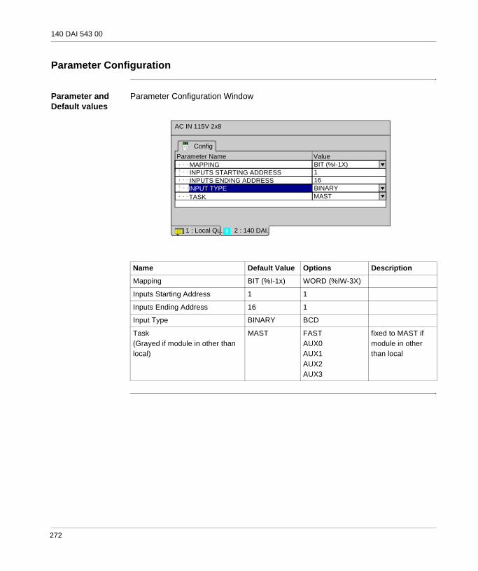
140 DAI 543 00
Parameter Configuration
Parameter and Default values
Parameter Configuration Window
Name Default Value Options Description
Mapping BIT (%I-1x) WORD (%IW-3X)
Inputs Starting Address 1 1
Inputs Ending Address 16 1
Input Type BINARY BCD
Task(Grayed if module in other than local)
MAST FASTAUX0AUX1AUX2AUX3
fixed to MAST if module in other than local
AC IN 115V 2x8
ConfigParameter Name Value
MAPPING BIT (%I-1X)INPUTS STARTING ADDRESS 1INPUTS ENDING ADDRESS 16INPUT TYPE BINARY
1 : Local Qu... 2 : 140 DAI.
TASK MAST
272

26
140 DAI 553 00: 115 VAC 4x8 IN ModuleOverview
Purpose The following chapter provides information of the Quantum 140 DAI 553 00 Module.
What's in this Chapter?
This chapter contains the following topics:
Topic Page
Presentation 274
Indicators 275
Wiring Diagram 276
Specifications 278
Parameter Configuration 280
273

140 DAI 553 00
Presentation
Function The AC Input 115 VAC 4x8 module accepts 115 VAC inputs.
Illustration The following figure shows the 140 DAI 553 00 module and its components.
1 Model Number, Module Description, Color Code
2 LED Display
3 Fuse Cutouts
4 Field Wiring Terminal Strip
5 Removable Door
6 Customer Identification Label (Fold label and place it inside door)
Note: The field wiring terminal strip (Modicon #140 XTS 002 00) must be ordered separately. (The terminal strip includes the removable door and label.)
140DAI 553 00
X X
XXXXXXXXXXXXXXXXXXXX
XXXXXXXXXXXXXXXXXXXXX
23
6
8
10
1214
16
18
20
21
232527
29
31
3335
37
1
4
7
9
11
13
1517
19
22
24
26
28
30
32
34
3638
1
2
3
4 5
6
274

140 DAI 553 00
Indicators
Illustration The following table shows the LED indicators for the 140 DAI 553 00 module.
Descriptions The following table shows the LED descriptions for the 140 DAI 553 00 module.
Active
91102113
1245678
13141516
LEDs Color Indication when ON
Active Green Bus communication is present.
1 ... 32 Green The indicated point or channel is turned ON.
275

140 DAI 553 00
Wiring Diagram
Illustration The following figure shows the 140 DAI 553 00 wiring diagram.
INPUT 12
10
4
6
8
12
14
16
18
20
22
24
26
28
30
32
34
36
38
40 39
37
35
33
31
29
27
25
23
21
19
17
15
13
11
9
7
5
3
1L NINPUT 2
INPUT 4
INPUT 6
INPUT 8
N/C
INPUT 10
INPUT 12
INPUT 14
INPUT 16
INPUT 18
INPUT 20
INPUT 22
INPUT 24
INPUT 26
INPUT 28
INPUT 30
INPUT 32
N/C
N/C
N/C
INPUT 3
INPUT 5
INPUT 7
GROUP A COMMON
GROUP B COMMON
GROUP C COMMON
GROUP D COMMON
INPUT 9
INPUT 11
INPUT 13
INPUT 15
INPUT 17
INPUT 19
INPUT 21
INPUT 23
INPUT 25
INPUT 27
INPUT 29
INPUT 31
276

140 DAI 553 00
Note: All inputs in a group must be from the same phase of line-input voltage.This module is not polarity sensitive.N / C = Not Connected.
Note: When field wiring the I/O module, the maximum wire size that should be used is 1-14 AWG or 2-16 AWG; the minimum size is 20 AWG.
CAUTIONVoltage CompatibilityAll inputs in a group must be from the same phase of line input voltage.Failure to follow this precaution can result in injury or equipment damage.
277
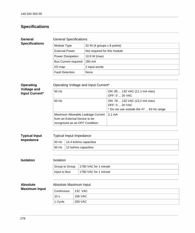
140 DAI 553 00
Specifications
General Specifications
General Specifications
Operating Voltage and Input Current*
Operating Voltage and Input Current*
Typical Input Impedance
Typical Imput Impedance
Isolation Isolation
Absolute Maximum Input
Absolute Maximum Input
Module Type 32 IN (4 groups x 8 points)
External Power Not required for this module
Power Dissipation 10.9 W (max)
Bus Current required 250 mA
I/O map 2 input words
Fault Detection None
50 Hz ON: 85 ... 132 VAC (11.1 mA max)OFF: 0 ... 20 VAC
60 Hz ON: 79 ... 132 VAC (13.2 mA max) OFF: 0 ... 20 VAC* Do not use outside the 47 ... 63 Hz range
Maximum Allowable Leakage Current from an External Device to be recognized as an OFF Condition.
2.1 mA
50 Hz 14.4 kohms capacitive
60 Hz 12 kohms capacitive
Group to Group 1780 VAC for 1 minute
Input to Bus 1780 VAC for 1 minute
Continuous 132 VAC
10 s 156 VAC
1 Cycle 200 VAC
278

140 DAI 553 00
Response Response
Fuses Fuses
OFF - ON Min: 4.9 ms. Max: 0.75 line cycle.
ON - OFF Min: 7.3 ms. Max: 12.3 ms.
Internal None
External User discretion
Note: Input signals must be sinusoidal with less than 6% THD and 63 Hz maximum frequency.
279

140 DAI 553 00
Parameter Configuration
Parameter and Default values
Parameter Configuration Window
Name Default Value Options Description
Mapping BIT (%I-1x) WORD (%IW-3X)
Inputs Starting Address 1 1
Inputs Ending Address 32 2
Input Type BINARY BCD
Task(Grayed if module in other than local)
MAST FASTAUX0AUX1AUX2AUX3
fixed to MAST if module in other than local
AC IN 115V 4x8
ConfigParameter Name Value
MAPPING BIT (%I-1X)INPUTS STARTING ADDRESS 1INPUTS ENDING ADDRESS 32INPUT TYPE BINARY
1 : Local Qu... 2 : 140 DAI.
TASK MAST
280
27
140 DAI 740 00: 230 VAC 16x1 IN ModuleOverview
Purpose The following chapter provides information of the Quantum 140 DAI 740 00 Module.
What's in this Chapter?
This chapter contains the following topics:
Topic Page
Presentation 282
Indicators 283
Wiring Diagram 284
Specifications 286
Parameter Configuration 288
281

140 DAI 740 00
Presentation
Function The AC Input 230 VAC 16x1 module accepts 230 VAC inputs.
Illustration The following figure shows the 140 DAI 740 00 module and its components.
1 Model Number, Module Description, Color Code
2 LED Display
3 Fuse Cutouts
4 Field Wiring Terminal Strip
5 Removable Door
6 Customer Identification Label (Fold label and place it inside door)
Note: The field wiring terminal strip (Modicon #140 XTS 002 00) must be ordered separately. (The terminal strip includes the removable door and label.)
140DAI 740 00
X X
XXXXXXXXXXXXXXXXXXXX
XXXXXXXXXXXXXXXXXXXXX
23
6
8
10
1214
16
18
20
21
232527
29
31
3335
37
1
4
7
9
11
13
1517
19
22
24
26
28
30
32
34
3638
1
2
3
4 5
6
282

140 DAI 740 00
Indicators
Illustration The following table shows the LED indicators for the 140 DAI 740 00 module.
Descriptions The following table shows the LED descriptions for the 140 DAI 740 00 module.
Active
91102113
1245678
13141516
LEDs Color Indication when ON
Active Green Bus communication is present.
1 ... 16 Green The indicated point or channel is turned ON.
283

140 DAI 740 00
Wiring Diagram
Illustration The following figure shows the 140 DAI 740 00 wiring diagram.
RETURN 1 INPUT 12
10
4
6
8
12
14
16
18
20
22
24
26
28
30
32
34
36
38
40 39
37
35
33
31
29
27
25
23
21
19
17
15
13
11
9
7
5
3
1RETURN 2
RETURN 3
RETURN 4
RETURN 5
RETURN 6
RETURN 7
RETURN 8
RETURN 9
RETURN 10
RETURN 11
RETURN 12
RETURN 13
RETURN 14
RETURN 15
RETURN 16
INPUT 2
INPUT 3
INPUT 4
INPUT 5
INPUT 6
INPUT 7
INPUT 8
INPUT 9
INPUT 10
INPUT 11
INPUT 12
INPUT 13
INPUT 14
INPUT 15
INPUT 16
N/C N/C
N/C
N/C
N/C
N/C
N/C
N/C
L N
284

140 DAI 740 00
Note: This module is not polarity sensitive.N / C = Not Connected.
Note: When field wiring the I/O module, the maximum wire size that should be used is 1-14 AWG or 2-16 AWG; the minimum size is 20 AWG.
285

140 DAI 740 00
Specifications
General Specifications
General Specifications
Operating Voltage and Input Current*
Operating Voltage and Input Current*
Typical Input Impedance
Typical Imput Impedance
Isolation Isolation
Absolute Maximum Input
Absolute Maximum Input
Module Type 16 IN (2 groups x 8 points) individually isolated
External Power Not required for this module
Power Dissipation 5.5 W (max)
Bus Current required 180 mA
I/O map 1 input word
Fault Detection None
50 Hz ON: 175 ... 264 VAC (9.7 mA max)OFF: 0 ... 40 VAC
60 Hz ON: 165 ... 264 VAC (11.5 mA max) OFF: 0 ... 40 VAC* Do not use outside the 47 ... 63 Hz range
Maximum Allowable Leakage Current from an External Device to be recognized as an OFF Condition.
2.6 mA
50 Hz 31.8 kohms capacitive
60 Hz 26.5 kohms capacitive
Input to Input 1780 VAC for 1 minute
Input to Bus 1780 VAC for 1 minute
Continuous 264 VAC
10 s 300 VAC
1 Cycle 400 VAC
286

140 DAI 740 00
Response Response
Fuses Fuses
OFF - ON Min: 4.9 ms. Max: 0.75 line cycle.
ON - OFF Min: 7.3 ms. Max: 12.3 ms.
Internal None
External User discretion
Note: Input signals must be sinusoidal with less than 6% THD and 63 Hz maximum frequency.
287

140 DAI 740 00
Parameter Configuration
Parameter and Default values
Parameter Configuration Window
Name Default Value Options Description
Mapping BIT (%I-1x) WORD (%IW-3X)
Inputs Starting Address 1 1
Inputs Ending Address 16 1
Input Type BINARY BCD
Task(Grayed if module in other than local)
MAST FASTAUX0AUX1AUX2AUX3
fixed to MAST if module in other than local
AC IN 230V 16x1
ConfigParameter Name Value
MAPPING BIT (%I-1X)INPUTS STARTING ADDRESS 1INPUTS ENDING ADDRESS 16INPUT TYPE BINARY
1 : Local Qu... 2 : 140 DAI.
TASK MAST
288

28
140 DAI 753 00: 230 VAC 4x8 IN ModuleOverview
Purpose The following chapter provides information of the Quantum 140 DAI 753 00 Module.
What's in this Chapter?
This chapter contains the following topics:
Topic Page
Presentation 290
Indicators 291
Wiring Diagram 292
Specifications 294
Parameter Configuration 296
289

140 DAI 753 00
Presentation
Function The AC Input 230 VAC 4x8 module accepts 230 VAC inputs.
Illustration The following figure shows the 140 DAI 753 00 module and its components.
1 Model Number, Module Description, Color Code
2 LED Display
3 Fuse Cutouts
4 Field Wiring Terminal Strip
5 Removable Door
6 Customer Identification Label (Fold label and place it inside door)
Note: The field wiring terminal strip (Modicon #140 XTS 002 00) must be ordered separately. (The terminal strip includes the removable door and label.)
140DAI 753 00
X X
XXXXXXXXXXXXXXXXXXXX
XXXXXXXXXXXXXXXXXXXXX
23
6
8
10
1214
16
18
20
21
232527
29
31
3335
37
1
4
7
9
11
13
1517
19
22
24
26
28
30
32
34
3638
1
2
3
4 5
6
290

140 DAI 753 00
Indicators
Illustration The following table shows the LED indicators for the 140 DAI 753 00 module.
Descriptions The following table shows the LED descriptions for the 140 DAI 753 00 module.
Active
91102113
1245678
13141516
171819
2021222324
252627
2829303132
LEDs Color Indication when ON
Active Green Bus communication is present.
1 ... 32 Green The indicated point or channel is turned ON.
291
140 DAI 753 00
Wiring Diagram
Illustration The following figure shows the 140 DAI 753 00 wiring diagram.
Note: N / C = Not Connected.
CAUTION
Voltage Compatibility
All inputs in a group must be from the same phase of line input voltage.
Failure to follow this precaution can result in injury or equipment damage.
2
10
4
6
8
12
14
16
18
20
22
24
26
28
30
32
34
36
38
40 39
37
35
33
31
29
27
25
23
21
19
17
15
13
11
9
7
5
3
1INPUT 4
INPUT 6
INPUT8
N/CINPUT 10
INPUT 12
INPUT 14
INPUT 16
INPUT 18
INPUT 20
INPUT 22
INPUT 24
INPUT 26
INPUT 28
INPUT 30
INPUT 32
INPUT 1
INPUT 3
INPUT 5
INPUT 7
GROUP A COMMON
INPUT 9
INPUT 11
INPUT 13
INPUT 15
INPUT 17
INPUT 19
INPUT 21
INPUT 23
INPUT 25
INPUT 27
INPUT 29
INPUT 31
GROUP B COMMON
GROUP C COMMON
GROUP D COMMON
L
N
INPUT 2
N/C
N/C
N/C
292

140 DAI 753 00
Note: When field wiring the I/O module, the maximum wire size that should be used is 1-14 AWG or 2-16 AWG; the minimum size is 20 AWG.
293
140 DAI 753 00
Specifications
General Specifications
General Specifications
Operating Voltage and Input Current*
Operating Voltage and Input Current*
Typical Input Impedance
Typical Imput Impedance
Isolation Isolation
Absolute Maximum Input
Absolute Maximum Input
Module Type 32 IN (4 groups x 8 points) individually isolated
External Power Not required for this module
Power Dissipation 9 W (max)
Bus Current required 250 mA
I/O map 1 input word
Fault Detection None
50 Hz ON: 175 ... 264 VAC (9.7 mA max)OFF: 0 ... 40 VAC
60 Hz ON: 165 ... 264 VAC (11.5 mA max) OFF: 0 ... 40 VAC* Do not use outside the 47 ... 63 Hz range
Maximum Allowable Leakage Current from an External Device to be recognized as an OFF Condition.
2.6 mA
50 Hz 32 kohms capacitive
60 Hz 27 kohms capacitive
Input to Input 1780 VAC for 1 minute
Input to Bus 1780 VAC for 1 minute
Continuous 264 VAC
10 s 300 VAC
1 Cycle 400 VAC
294
140 DAI 753 00
Response Response
Fuses Fuses
OFF - ON Min: 4.9 ms. Max: 0.75 line cycle.
ON - OFF Min: 7.3 ms. Max: 12.3 ms.
Internal None
External User discretion
Note: Input signals must be sinusoidal with less than 6% THD and 63 Hz maximum frequency.
295

140 DAI 753 00
Parameter Configuration
Parameter and Default values
Parameter Configuration Window
Name Default Value Options Description
Mapping BIT (%I-1x) WORD (%IW-3X)
Inputs Starting Address 1 1
Inputs Ending Address 32 2
Input Type BINARY BCD
Task(Grayed if module in other than local)
MAST FASTAUX0AUX1AUX2AUX3
fixed to MAST if module in other than local
AC IN 230V 4x8
ConfigParameter Name Value
MAPPING BIT (%I-1X)INPUTS STARTING ADDRESS 1INPUTS ENDING ADDRESS 32INPUT TYPE BINARY
1 : Local Qu... 2 : 140 DAI.
TASK MAST
296
29
140 DSI 353 00: 24 VDC 2x16 Supervised IN ModuleOverview
Purpose The following chapter provides information of the Quantum 140 DSI 353 00 Module.
What's in this Chapter?
This chapter contains the following topics:
Topic Page
Presentation 298
Indicators 299
Wiring Diagram 300
Specifications 302
Addressing 303
Parameter Configuration 305
297

140 DSI 353 00
Presentation
Function The 140 DSI 353 00 module is used with source output devices. It accepts 24 VDC inputs. It has 32 input points (four groups of 8), and has broken wire detection for each unit.
Illustration The following figure shows the 140 DSI 353 00 module and its components.
1 Model Number, Module Description, Color Code2 LED Display3 Fuse Cutouts4 Field Wiring Terminal Strip5 Removable Door6 Customer Identification Label (Fold label and place it inside door)
Note: The field wiring terminal strip (Modicon #140 XTS 002 00) must be ordered separately. (The terminal strip includes the removable door and label.)
Note: In the DIO rack with 140 CRA 211 x0 module, 140 DSI 353 00 module must not be used.
140DSI 353 00
X X
XXXXXXXXXXXXXXXXXXXX
XXXXXXXXXXXXXXXXXXXXX
23
6
8
10
1214
16
18
20
21
232527
29
31
3335
37
1
4
7
9
11
13
1517
19
22
24
26
28
30
32
34
3638
1
2
3
4 5
6
298

140 DSI 353 00
Indicators
Illustration The following table shows the LED indicators for the 140 DSI 353 00 module.
Descriptions The following table shows the LED descriptions for the 140 DSI 353 00 module.
Active F
91102113
1245678
13141516
171819
2021222324
252627
2829303132
LEDs Color Indication when ON
Active Green Bus communication is present.
F Red A fault (external to the module) has been detected.
1 ... 32 Green The indicated point or channel is turned ON.
299

140 DSI 353 00
Wiring Diagram
Wiring Diagram Wiring diagram for the 140 DSI 353 00 Module:
OUTPUT 3
OUTPUT 15
GROUP B COMMON
GROUP C SUPPLY
GROUP D SUPPLY
2
10
4
6
8
12
14
16
18
20
22
24
26
28
30
32
34
36
38
40 39
37
35
33
31
29
27
25
23
21
19
17
15
13
11
9
7
5
3
1 OUTPUT 1
OUTPUT 5
OUTPUT 7
GROUP A COMMON
OUTPUT 9
OUTPUT 11
OUTPUT 13
GROUP C COMMON
GROUP D COMMON
OUTPUT 17
OUTPUT 19
OUTPUT 21
OUTPUT 23
OUTPUT 25
OUTPUT 27
OUTPUT 29
OUTPUT 31OUTPUT 32
OUTPUT 30
OUTPUT 28
OUTPUT 26
OUTPUT 24
OUTPUT 22
OUTPUT 20
OUTPUT 18
GROUP B SUPPLY
OUTPUT 16
OUTPUT 14
OUTPUT 12
OUTPUT 10
GROUP A SUPPLY
OUTPUT 8
OUTPUT 6
OUTPUT 4
OUTPUT 2
* 56 KΩ
* 56 KΩ
+
300

140 DSI 353 00
* Recommended resistor value for 24V DC
Note: When field wiring the I/O module, the maximum wire size that should be used is 1-14 AWG or 2-16 AWG; the minimum size is 20 AWG.
301
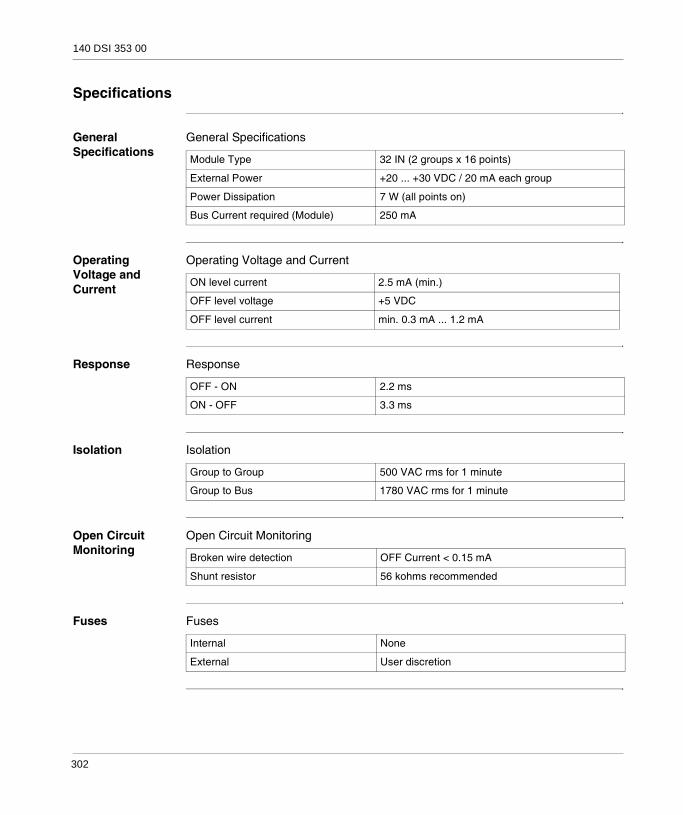
140 DSI 353 00
Specifications
General Specifications
General Specifications
Operating Voltage and Current
Operating Voltage and Current
Response Response
Isolation Isolation
Open Circuit Monitoring
Open Circuit Monitoring
Fuses Fuses
Module Type 32 IN (2 groups x 16 points)
External Power +20 ... +30 VDC / 20 mA each group
Power Dissipation 7 W (all points on)
Bus Current required (Module) 250 mA
ON level current 2.5 mA (min.)
OFF level voltage +5 VDC
OFF level current min. 0.3 mA ... 1.2 mA
OFF - ON 2.2 ms
ON - OFF 3.3 ms
Group to Group 500 VAC rms for 1 minute
Group to Bus 1780 VAC rms for 1 minute
Broken wire detection OFF Current < 0.15 mA
Shunt resistor 56 kohms recommended
Internal None
External User discretion
302
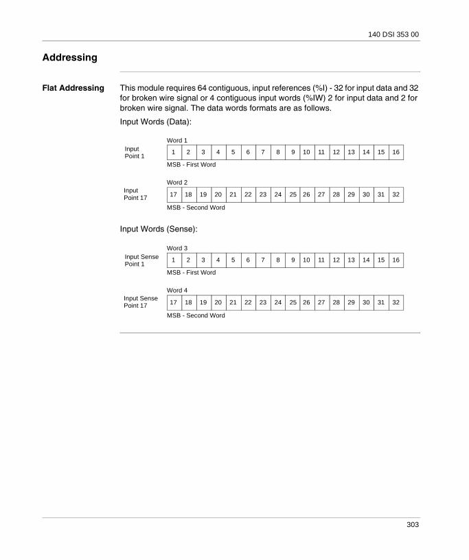
140 DSI 353 00
Addressing
Flat Addressing This module requires 64 contiguous, input references (%I) - 32 for input data and 32 for broken wire signal or 4 contiguous input words (%IW) 2 for input data and 2 for broken wire signal. The data words formats are as follows.
Input Words (Data):
Input Words (Sense):
1 2 3 4 5 6 7 10 11 12 13 14 15 168 9
17 18 19 20 21 22 23 26 27 28 29 30 31 3224 25
Input Point 1
Word 2
MSB - First Word
Word 1
MSB - Second Word
InputPoint 17
1 2 3 4 5 6 7 10 11 12 13 14 15 168 9
17 18 19 20 21 22 23 26 27 28 29 30 31 3224 25
Input SensePoint 1
Word 4
MSB - First Word
Word 3
MSB - Second Word
Input SensePoint 17
303

140 DSI 353 00
Topological Addressing
Topological addresses in Bit Mapping format:
Topological addresses in Word Mapping format:
Used abbreviations: b = bus, e = equipment (drop), r = rack, m = module slot.
I/O Map Status Byte
The eight bits in the I/O map status byte are used as follows:
Point I/O Object Comment
Input 1 %I[\b.e\]r.m.1.1 Value
Input 2 %I[\b.e\]r.m.2.1 Value
• • •
Input 31 %I[\b.e\]r.m.31.1 Value
Input 32 %I[\b.e\]r.m.32.1 Value
Broken Wire 1 %I[\b.e\]r.m.1.2 Value
Broken Wire 2 %I[\b.e\]r.m..2.2 Value
• • •
Broken Wire 31 %I[\b.e\]r.m.31.2 Value
Broken Wire 32 %I[\b.e\]r.m.32.2 Value
Point I/O Object Comment
Inputword 1 %IW[\b.e\]r.m.1.1 Value
Inputword 2 %IW[\b.e\]r.m.1.2 Value
Inputword 3 %IW[\b.e\]r.m.1.3 Broken Wire Flag
Inputword 4 %IW[\b.e\]r.m.1.4 Broken Wire Flag
8 7 6 5 4 3 2 1
Group B Broken WireGroup C Broken Wire
Group D Broken Wire
Group A Broken Wire
304

140 DSI 353 00
Parameter Configuration
Parameter and Default values
Parameter Configuration Window
Name Default Value Options Description
Mapping BIT (%I-1x) WORD (%IW-3X)
Inputs Starting Address
1 1
Inputs Ending Address
64 4
Task(Grayed if module in other than local)
Mast Fast fixed to Mast if module in other than local
Supervised 24V DC Input
Config
Parameter Name ValueMAPPING WORD (%IW-3X)INPUTS STARTING ADDRESS 1INPUTS ENDING ADDRESS 64TASK MAST
1 : Local Qu... 2 : 140 DSI...
305

140 DSI 353 00
306

VI
Discrete OUT ModulesAt a Glance
Introduction The following part provides information on the Quantum Discrete OUT modules.
What's in this Part?
This part contains the following chapters:
Chapter Chapter Name Page
30 General Information 309
31 140 DDO 153 10: 5 VDC 4x8 TTL Sink OUT Module 311
32 140 DDO 353 00: 24 VDC 4x8 Source OUT Module 319
33 140 DDO 353 01: 24 VDC 4x8 Source OUT Module 329
34 140 DDO 353 10: 24 VDC 4x8 Sink OUT Module 339
35 140 DDO 364 00: 24 VDC 6x16 Telefast OUT Module 349
36 140 DDO 843 00: 10 ... 60 VDC 2x8 Source OUT Module 359
37 140 DDO 885 00: 24 ... 125 VDC 2x6 Source OUT Module 367
38 140 DAO 840 00: 24 ... 230 VAC 16x1 OUT Module 379
39 140 DAO 840 10: 24 ... 115 VAC 16x1 OUT Module 389
40 140 DAO 842 10: 100 ... 230 VAC 4x4 OUT Module 399
41 140 DAO 842 20: 24 ... 48 VAC 4x4 OUT Module 409
42 140 DAO 853 00: 230 VAC 4x8 Source OUT Module 419
43 140 DRA 840 00: Relay 16x1 Normally Open OUT Module 429
44 140 DRC 830 00: Relay 8x1 Normally Open / Normally Closed OUT Module
437
45 140 DVO 853 00: 10 ... 30 VDC 32x1 Verified OUT Module 447
307

Discrete OUT Modules
308

30
General InformationDiscrete I/O Logic Circuits
Discrete I/O True High Figure
The following figure shows true high/current sink input/current source output schematic.
Discrete I/O True Low Figure
The following figure shows true low/current source input/current sink output schematic.
Power Supply
+
Load
Output
Current
LOGIC
Input
Current
Common
Power Supply
+
+
Power Supply
Load
Output
Current
LOGIC
Input
Current
Power Supply
+
Common
309

General Information
Current Sinking This describes a physical implementation of the I/O hardware, which when in the true state, sinks current from the external load.
Current Sourcing This describes a physical implementation of the I/O hardware, which when in the true state, sources current to the external load.
310

31
140 DDO 153 10: 5 VDC 4x8 TTL Sink OUT ModuleOverview
Purpose The following chapter provides information of the Quantum 140 DDO 153 10 Module.
What's in this Chapter?
This chapter contains the following topics:
Topic Page
Presentation 312
Indicators 313
Wiring Diagram 314
Specifications 316
Maintenance 317
140 DDO 153 10 Parameter Configuration 318
311

140 DDO 153 10
Presentation
Function The DC Output 5 V TTL 4x8 Sink module switches 5 VDC loads and is for use with source devices and is compatible with LS, S, TTL, and CMOS logic.
Illustration The following figure shows the 140 DDO 153 10 module and its components.
1 Model Number, Module Description, Color Code
2 LED Display
3 Fuse Cutouts
4 Field Wiring Terminal Strip
5 Removable Door
6 Customer Identification Label (Fold label and place it inside door)
Note: The field wiring terminal strip (Modicon #140 XTS 002 00) must be ordered separately. (The terminal strip includes the removable door and label.)
140DDO 153 10
X X
XXXXXXXXXXXXXXXXXXXX
XXXXXXXXXXXXXXXXXXXXX
23
6
8
10
1214
16
18
20
21
232527
29
31
3335
37
1
4
7
9
11
13
1517
19
22
24
26
28
30
32
34
3638
1
2
3
4 5
6
312

140 DDO 153 10
Indicators
Illustration The following table shows the LED indicators for the 140 DDO 153 10 module.
Descriptions The following table shows the LED descriptions for the 140 DDO 153 10 module.
Active F
91102113
1245678
13141516
171819
2021222324
252627
2829303132
LEDs Color Indication when ON
Active Green Bus communication is present.
F Red A fault (external to the module) has been detected.
1 ... 32 Green The indicated point or channel is turned ON.
313

140 DDO 153 10
Wiring Diagram
Illustration The following figure shows the 140 DDO 153 10 wiring diagram.
2
10
4
6
8
12
14
16
18
20
22
24
26
28
30
32
34
36
38
40 39
37
35
33
31
29
27
25
23
21
19
17
15
13
11
9
7
5
3
1
+ -
TTL Inverter
TTL Nand Gate
US5 Vdc
OUTPUT 1
OUTPUT 3
OUTPUT 5
OUTPUT 7
GROUP A COMMON
OUTPUT 9
OUTPUT 11
OUTPUT 13
OUTPUT 15
OUTPUT 17
OUTPUT 19
OUTPUT 21
OUTPUT 23
GROUP B COMMON
GROUP C COMMON
GROUP D COMMON
OUTPUT 25
OUTPUT 27
OUTPUT 29
OUTPUT 31OUTPUT 32
GROUP D SUPPLY
OUTPUT 30
OUTPUT 28
OUTPUT 26
GROUP C SUPPLY
OUTPUT 24
OUTPUT 22
OUTPUT 20
OUTPUT 18
OUTPUT 16
OUTPUT 14
OUTPUT 12
OUTPUT 10
GROUP B SUPPLY
GROUP A SUPPLY
OUTPUT 8
OUTPUT 6
OUTPUT 4
OUTPUT 2
314

140 DDO 153 10
Note: When field wiring the I/O module, the maximum wire size that should be used is 1-14 AWG or 2-16 AWG; the minimum size is 20 AWG.
315

140 DDO 153 10
Specifications
General Specifications
General Specifications
Input Rating Input Rating
Maximum Load Current / Surge Current
Maximum Load Current / Surge Current
Isolation / Protection
Isolation / Protection
Response Response
Module Type 32 OUT (4 groups x 8 points)
Logic True Low
External Power (Us) 4.5 ... 5.5 VDC continuous
Absolute Voltage (Us) 15 VDC for 1.3 ms decaying pulse
Power Dissipation 4 W
Supply Current 400 mA + Load Current per Point
Bus Current required (Module) 350 mA
I/O map 2 output word
Fault Detection Output: Blown fuse detect, loss of field power.
ON level voltage 0.2 VDC (max.) @ 75 mA sinking
OFF level voltage Vout = Us - 1.25 V @ 1 mA source Vout = 3.2 V (min.) @ 1 mA, Us = 4.5 V
Internal Pullup Resistor 440 ohm
Each Point 75 mA (sinking)
Each Group 600 mA
Per Module 2.4 A
Surge Current (max.) Each Point: 75 mA @ 500 ms duration (no more than 6 per minute)
Group to Group 500 VAC rms for 1 minute
Group to Bus 1780 VAC rms for 1 minute
Output Protection Transient Voltage Suppression (internal)
OFF - ON 250 μs (max) - (resistive load)
ON - OFF 250 μs (max) - (resistive load)
316

140 DDO 153 10
Maintenance
Fuses Fuses
Illustration The following figure shows the locations of the fuses for the 140 DDO 153 10 module.
Internal 1 A fuse for each group. (Part # 043508953) or equivalent). For the location of the fuses see figure below.
External None
CAUTIONPossible danger to equipment or personnel.Turn off power to the module and remove the field wiring terminal strip to gain access to fuses.Failure to follow this precaution can result in injury or equipment damage.
140DDO 153 10
X
Fuse LocationsPoints
1-8
Points9-16
Points17-24
Points25-32
317
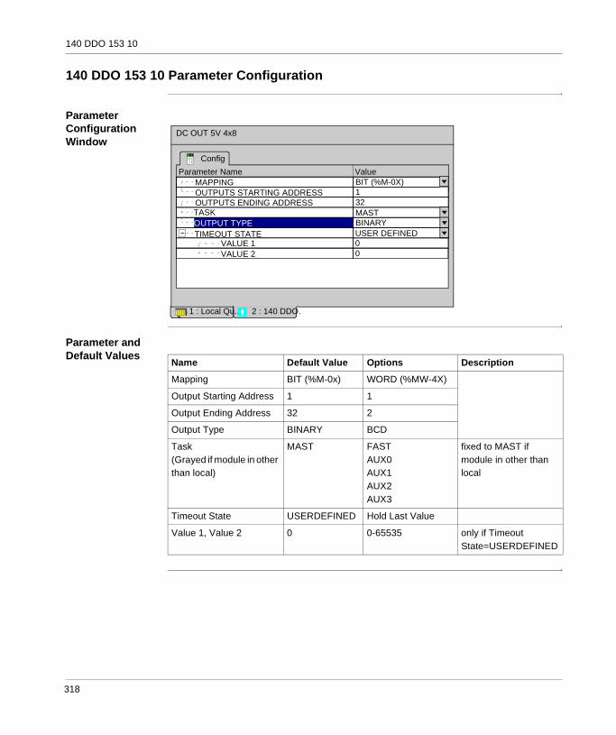
140 DDO 153 10
140 DDO 153 10 Parameter Configuration
Parameter Configuration Window
Parameter and Default Values
DC OUT 5V 4x8
ConfigParameter Name Value
MAPPING BIT (%M-0X)OUTPUTS STARTING ADDRESS 1OUTPUTS ENDING ADDRESS 32
OUTPUT TYPE BINARY
1 : Local Qu... 2 : 140 DDO.
TIMEOUT STATE USER DEFINEDVALUE 1VALUE 2
TASK MAST
00
Name Default Value Options Description
Mapping BIT (%M-0x) WORD (%MW-4X)
Output Starting Address 1 1
Output Ending Address 32 2
Output Type BINARY BCD
Task(Grayed if module in other than local)
MAST FASTAUX0AUX1AUX2AUX3
fixed to MAST if module in other than local
Timeout State USERDEFINED Hold Last Value
Value 1, Value 2 0 0-65535 only if Timeout State=USERDEFINED
318

32
140 DDO 353 00: 24 VDC 4x8 Source OUT ModuleOverview
Purpose The following chapter provides information of the Quantum 140 DDO 353 00 Module.
What's in this Chapter?
This chapter contains the following topics:
Topic Page
Presentation 320
Indicators 321
Wiring Diagram 322
Specifications 324
Maintenance 326
140 DDO 353 00 Parameter Configuration 327
319

140 DDO 353 00
Presentation
Function The DC Output 24 VDC 4x8 Source module switches 24 VDC powered loads and is for use with sink devices.
Illustration The following figure shows the 140 DDO 353 00 module and its components.
1 Model Number, Module Description, Color Code
2 LED Display
3 Fuse Cutouts
4 Field Wiring Terminal Strip
5 Removable Door
6 Customer Identification Label (Fold label and place it inside door)
Note: The field wiring terminal strip (Modicon #140 XTS 002 00) must be ordered separately. (The terminal strip includes the removable door and label.)
140DDO 353 00
X X
XXXXXXXXXXXXXXXXXXXX
XXXXXXXXXXXXXXXXXXXXX
23
6
8
10
1214
16
18
20
21
232527
29
31
3335
37
1
4
7
9
11
13
1517
19
22
24
26
28
30
32
34
3638
1
2
3
4 5
6
320

140 DDO 353 00
Indicators
Illustration The following table shows the LED indicators for the 140 DDO 353 00 module.
Descriptions The following table shows the LED descriptions for the 140 DDO 353 00 module.
Active F
91102113
1245678
13141516
171819
2021222324
252627
2829303132
LEDs Color Indication when ON
Active Green Bus communication is present.
F Red A fault (external to the module) has been detected.
1 ... 32 Green The indicated point or channel is turned ON.
321

140 DDO 353 00
Wiring Diagram
Illustration The following figure shows the 140 DDO 353 00 wiring diagram.
-2
10
4
6
8
12
14
16
18
20
22
24
26
28
30
32
34
36
38
40 39
37
35
33
31
29
27
25
23
21
19
17
15
13
11
9
7
5
3
1+
3/4 A
3/4 A
OUTPUT 1
OUTPUT 3
OUTPUT 5
OUTPUT 7
GROUP A COMMON
OUTPUT 9
OUTPUT 11
OUTPUT 13
OUTPUT 15
GROUP B COMMON
GROUP C COMMON
GROUP D COMMON
OUTPUT 17
OUTPUT 19
OUTPUT 21
OUTPUT 23
OUTPUT 25
OUTPUT 27
OUTPUT 29
OUTPUT 31OUTPUT 32
GROUP D SUPPLY
OUTPUT 30
OUTPUT 28
OUTPUT 26
GROUP C SUPPLY
OUTPUT 24
OUTPUT 22
OUTPUT 20
OUTPUT 18
GROUP B SUPPLY
OUTPUT 16
OUTPUT 14
OUTPUT 12
OUTPUT 10
GROUP A SUPPLY
OUTPUT 8
OUTPUT 6
OUTPUT 4
OUTPUT 2
FIELD DEVICE
+ -
322

140 DDO 353 00
CAUTIONPossible Equipment FailureEach group is protected with a 5 A fuse to protect the module from catastrophic failure. The group fuse will not be guaranteed to protect each output switch for all possible overload conditions. It is recommended that each point be protected with a 3/4 A, 250 V fuse (Part # 57-0078-000). Failure to follow this precaution can result in injury or equipment damage.
CAUTIONElectrical shock hazardTurn off power to the module and remove the field wiring terminal strip to gain access to fuses.Failure to follow this precaution can result in injury or equipment damage.
Note: When field wiring the I/O module, the maximum wire size that should be used is 1-14 AWG or 2-16 AWG; the minimum size is 20 AWG.
323

140 DDO 353 00
Specifications
General Specifications
General Specifications
Voltage Voltage
Maximum Load Current / Surge Current
Maximum Load Current / Surge Current
Isolation / Protection
Isolation / Protection
Module Type 32 OUT (4 groups x 8 points)
Logic True High
External Power 19.2 ... 30 VDC
Power Dissipation 1.75 W + 0.4 V x Total module load Current
Bus Current required (Module) 330 mA
I/O map 2 output word
Fault Detection Output: Blown fuse detect, loss of field power.
Operating Voltage (max.) 19.2 ... 30 VDC
Absolute Voltage (max.) 56 VDC for 1 ms decaying pulse
ON State Drop / Point 0.4 VDC @ 0.5 A
Each Point 0.5 A
Each Group 4 A
Per Module 16 A
Surge Current (max.) Each Point: 5 mA @ 500 ms duration (no more than 6 per minute)
OFF State Leakage / Point 0.4 mA @ 30 VDC
Group to Group 500 VAC rms for 1 minute
Group to Bus 1780 VAC rms for 1 minute
Output Protection Transient Voltage Suppression (internal)
324

140 DDO 353 00
Response (Resistive Loads)
Response (Resistive Loads)
Load Inductance / Capacitance (max.)
Load Inductance / Capacitance (max.)
OFF - ON 1 ms (max.)
ON - OFF 1 ms (max.)
Load Inductance (max.)
0.5 Henry @ 4 Hz switch frequency, or:
Load Capacitance (max.)
50 μF
L = 0.5
l2 F
where: L = Load inductance (henry) l = Load current (A)
F = Switching Frequency (Hz)
325

140 DDO 353 00
Maintenance
Fuses Fuses
Illustration The following figure shows the fuse locations for the 140 DDO 353 00 module.
Internal 5 A fuse for each group. (Part # 043502405) or equivalent). For the location of the fuses see figure below.
External Each group is protected with a 5A fuse to protect the module from catastrophic failure. The group fuse is not guaranteed to protect each output switch for all possible overload conditions. It is recommended that each point be protected with a 3/4 A, 250 V fuse (Part # 57-0078-000).
CAUTIONPossible danger to equipment or personnel.Turn off power to the module and remove the field wiring terminal strip to gain access to fuses.Failure to follow this precaution can result in injury or equipment damage.
140DDO 353 10
X
Fuse LocationsPoints
1-8
Points9-16
Points17-24
Points25-32
326

140 DDO 353 00
140 DDO 353 00 Parameter Configuration
Parameter Configuration Window
Parameter and Default Values
DC OUT 24V 4x8
ConfigParameter Name Value
MAPPING BIT (%M-0X)OUTPUTS STARTING ADDRESS 1OUTPUTS ENDING ADDRESS 32
OUTPUT TYPE BINARY
1 : Local Qu... 2 : 140 DDO.
TIMEOUT STATE USER DEFINEDVALUE 1VALUE 2
TASK MAST
00
Name Default Value Options Description
Mapping BIT (%M-0x) WORD (%MW-4X)
Output Starting Address 1 1
Output Ending Address 32 2
Output Type BINARY BCD
Task(Grayed if module in other than local)
MAST FASTAUX0AUX1AUX2AUX3
fixed to MAST if module in other than local
Timeout State USERDEFINED HOLD LAST VALUE
Value 1, Value 2 0 0-65535 only if Timeout State=USERDEFINED
327

140 DDO 353 00
328

33
140 DDO 353 01: 24 VDC 4x8 Source OUT ModuleOverview
Purpose The following chapter provides information of the Quantum 140 DDO 353 01 Module.
What's in this Chapter?
This chapter contains the following topics:
Topic Page
Presentation 330
Indicators 331
Wiring Diagram 332
Specifications 334
Maintenance 336
140 DDO 353 01 Parameter Configuration 337
329

140 DDO 353 01
Presentation
Function The 140 DDO 353 01 source module switches 24 VDC powered loads, and is short circuit and overload resistant.
Illustration The following figure shows the 140 DDO 353 01 module and its components.
1 Model Number, Module Description, Color Code
2 LED Display
3 Fuse Cutouts
4 Field Wiring Terminal Strip
5 Removable Door
6 Customer Identification Label (Fold label and place it inside door)
Note: The field wiring terminal strip (Modicon #140 XTS 002 00) must be ordered separately. (The terminal strip includes the removable door and label.)
140DDO 353 01
X X
XXXXXXXXXXXXXXXXXXXX
XXXXXXXXXXXXXXXXXXXXX
23
6
8
10
1214
16
18
20
21
232527
29
31
3335
37
1
4
7
9
11
13
1517
19
22
24
26
28
30
32
34
3638
1
2
3
4 5
6
330

140 DDO 353 01
Indicators
Illustration The following table shows the LED indicators for the 140 DDO 353 01 module.
Descriptions The following table shows the LED descriptions for the 140 DDO 353 01 module.
Active F
91102113
1245678
13141516
171819
2021222324
252627
2829303132
LEDs Color Indication when ON
Active Green Bus communication is present.
F Red A fault (external to the module) has been detected.
1 ... 32 Green The indicated point or channel is turned ON.
331

140 DDO 353 01
Wiring Diagram
Illustration The following figure shows the 140 DDO 353 01 wiring diagram.
-2
10
4
6
8
12
14
16
18
20
22
24
26
28
30
32
34
36
38
40 39
37
35
33
31
29
27
25
23
21
19
17
15
13
11
9
7
5
3
1+
3/4 A
3/4 A
OUTPUT 1
OUTPUT 3
OUTPUT 5
OUTPUT 7
GROUP A COMMON
OUTPUT 9
OUTPUT 11
OUTPUT 13
OUTPUT 15
GROUP B COMMON
GROUP C COMMON
GROUP D COMMON
OUTPUT 17
OUTPUT 19
OUTPUT 21
OUTPUT 23
OUTPUT 25
OUTPUT 27
OUTPUT 29
OUTPUT 31OUTPUT 32
GROUP D SUPPLY
OUTPUT 30
OUTPUT 28
OUTPUT 26
GROUP C SUPPLY
OUTPUT 24
OUTPUT 22
OUTPUT 20
OUTPUT 18
GROUP B SUPPLY
OUTPUT 16
OUTPUT 14
OUTPUT 12
OUTPUT 10
GROUP A SUPPLY
OUTPUT 8
OUTPUT 6
OUTPUT 4
OUTPUT 2
FIELD DEVICE
+ -
332

140 DDO 353 01
CAUTIONPossible Equipment FailureEach group is protected with a 5 A fuse to protect the module from catastrophic failure. Failure to follow this precaution can result in injury or equipment damage.
CAUTIONElectrical shock hazardDisconnect the supply voltage to the module and remove the field wiring terminal strip to gain access to fuses.Failure to follow this precaution can result in injury or equipment damage.
Note: When field wiring the I/O module, the maximum wire size that should be used is 1-14 AWG or 2-16 AWG; the minimum size is 20 AWG.
333
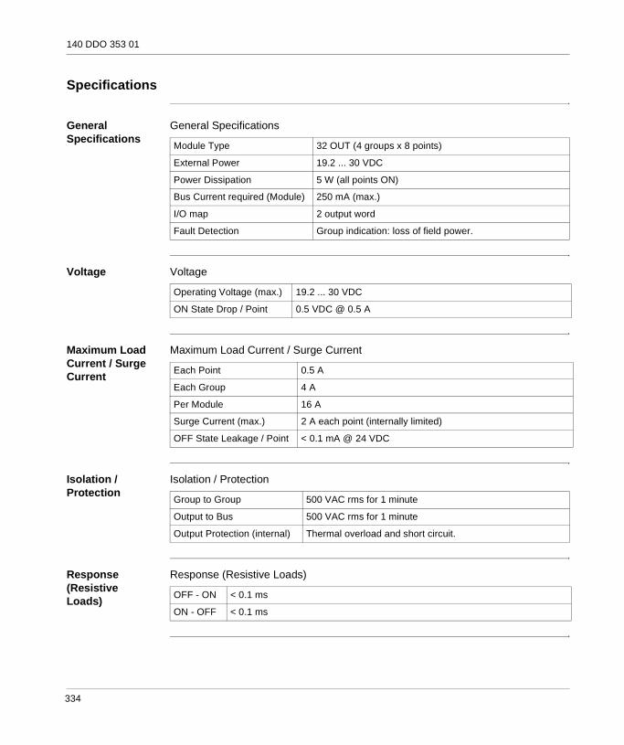
140 DDO 353 01
Specifications
General Specifications
General Specifications
Voltage Voltage
Maximum Load Current / Surge Current
Maximum Load Current / Surge Current
Isolation / Protection
Isolation / Protection
Response (Resistive Loads)
Response (Resistive Loads)
Module Type 32 OUT (4 groups x 8 points)
External Power 19.2 ... 30 VDC
Power Dissipation 5 W (all points ON)
Bus Current required (Module) 250 mA (max.)
I/O map 2 output word
Fault Detection Group indication: loss of field power.
Operating Voltage (max.) 19.2 ... 30 VDC
ON State Drop / Point 0.5 VDC @ 0.5 A
Each Point 0.5 A
Each Group 4 A
Per Module 16 A
Surge Current (max.) 2 A each point (internally limited)
OFF State Leakage / Point < 0.1 mA @ 24 VDC
Group to Group 500 VAC rms for 1 minute
Output to Bus 500 VAC rms for 1 minute
Output Protection (internal) Thermal overload and short circuit.
OFF - ON < 0.1 ms
ON - OFF < 0.1 ms
334

140 DDO 353 01
Load Inductance / Capacitance (max.)
Load Inductance / Capacitance (max.)
Load Inductance (max.) 0.5 Henry @ 4 Hz switch frequency, or:
Load Capacitance (max.) 50 μF
L = 0.5
l2 F
where: L = Load inductance (henry) l = Load current (A)
F = Switching Frequency (Hz)
335

140 DDO 353 01
Maintenance
Fuses Fuses
Illustration The following figure shows the fuse locations for the 140 DDO 353 00 module.
Internal 5 A fuse for each group. (Part # 043502405) or equivalent). For the location of the fuses see figure below.
External User discretion
CAUTIONPossible danger to equipment or personnel.Disconnect the supply voltage to the module and remove the field wiring terminal strip to gain access to fuses.Failure to follow this precaution can result in injury or equipment damage.
140DDO 353 10
X
Fuse LocationsPoints
1-8
Points9-16
Points17-24
Points25-32
336

140 DDO 353 01
140 DDO 353 01 Parameter Configuration
Parameter Configuration Window
Parameter and Default Values
DC OUT 24V 4x8
ConfigParameter Name Value
MAPPING BIT (%M-0X)OUTPUTS STARTING ADDRESS 1OUTPUTS ENDING ADDRESS 32
OUTPUT TYPE BINARY
1 : Local Qu... 2 : 140 DDO.
TIMEOUT STATE USER DEFINEDVALUE 1VALUE 2
TASK MAST
00
Name Default Value Options Description
Mapping BIT (%M-0x) WORD (%MW-4X)
Output Starting Address 1 1
Output Ending Address 32 2
Output Type BINARY BCD
Task(Grayed if module in other than local)
MAST FASTAUX0AUX1AUX2AUX3
fixed to MAST if module in other than local
Timeout State USERDEFINED HOLD LAST VALUE
Value 1, Value 2 0 0-65535 only if Timeout State=USERDEFINED
337

140 DDO 353 01
338

34
140 DDO 353 10: 24 VDC 4x8 Sink OUT ModuleOverview
Purpose The following chapter provides information of the Quantum 140 DDO 353 10 Module.
What's in this Chapter?
This chapter contains the following topics:
Topic Page
Presentation 340
Indicators 341
Wiring Diagram 342
Specifications 344
Maintenance 346
140 DDO 353 10 Parameter Configuration 347
339

140 DDO 353 10
Presentation
Function The 24 VDC True Low 4x8 Output module switches 24 VDC loads capable of driving displays, logic, and other loads up to 500 mA sinking, in the ON state.
Illustration The following figure shows the 140 DDO 353 10 module and its components.
1 Model Number, Module Description, Color Code
2 LED Display
3 Fuse Cutouts
4 Field Wiring Terminal Strip
5 Removable Door
6 Customer Identification Label (Fold label and place it inside door)
Note: The field wiring terminal strip (Modicon #140 XTS 002 00) must be ordered separately. (The terminal strip includes the removable door and label.)
140DDO 353 10
X X
XXXXXXXXXXXXXXXXXXXX
XXXXXXXXXXXXXXXXXXXXX
23
6
8
10
1214
16
18
20
21
232527
29
31
3335
37
1
4
7
9
11
13
1517
19
22
24
26
28
30
32
34
3638
1
2
3
4 5
6
340

140 DDO 353 10
Indicators
Illustration The following table shows the LED indicators for the 140 DDO 353 10 module.
Descriptions The following table shows the LED descriptions for the 140 DDO 353 10 module.
Active F
91102113
1245678
13141516
171819
2021222324
252627
2829303132
LEDs Color Indication when ON
Active Green Bus communication is present.
F Red A fault (external to the module) has been detected.
1 ... 32 Green The indicated point or channel is turned ON.
341

140 DDO 353 10
Wiring Diagram
Illustration The following figure shows the 140 DDO 353 10 wiring diagram.
-2
10
4
6
8
12
14
16
18
20
22
24
26
28
30
32
34
36
38
40 39
37
35
33
31
29
27
25
23
21
19
17
15
13
11
9
7
5
3
1+
1 A
1 A
OUTPUT 1
OUTPUT 3
OUTPUT 5
OUTPUT 7
GROUP A COMMON
OUTPUT 9
OUTPUT 11
OUTPUT 13
OUTPUT 15
GROUP B COMMON
GROUP C COMMON
GROUP D COMMON
OUTPUT 17
OUTPUT 19
OUTPUT 21
OUTPUT 23
OUTPUT 25
OUTPUT 27
OUTPUT 29
OUTPUT 31OUTPUT 32
GROUP D SUPPLY
OUTPUT 30
OUTPUT 28
OUTPUT 26
GROUP C SUPPLY
OUTPUT 24
OUTPUT 22
OUTPUT 20
OUTPUT 18
GROUP B SUPPLY
OUTPUT 16
OUTPUT 14
OUTPUT 12
OUTPUT 10
GROUP A SUPPLY
OUTPUT 8
OUTPUT 6
OUTPUT 4
OUTPUT 2
FIELD DEVICE
+ -
-24 Vdc
1 A
342

140 DDO 353 10
CAUTIONPossible Equipment FailureEach group is protected with a 5 A fuse to protect the module from catastrophic failure. The group fuse will not be guaranteed to protect each output switch for all possible overload conditions. It is recommended that each point be fused with a 3/4 A, 250 V fuse Part # 57-0078-000.Failure to follow this precaution can result in injury or equipment damage.
Note: When field wiring the I/O module, the maximum wire size that should be used is 1-14 AWG or 2-16 AWG; the minimum size is 20 AWG.
343

140 DDO 353 10
Specifications
General Specifications
General Specifications
Voltage Voltage
Maximum Load Current / Surge Current
Maximum Load Current / Surge Current
Isolation / Protection
Isolation / Protection
Response (Resistive Loads)
Response (Resistive Loads)
Module Type 32 OUT (4 groups x 8 points)
Logic True Low
External Power 19.2 ... 30 VDC
Power Dissipation 2.0 W + (0.4 V x Total load Current)
Bus Current required (Module) 330 mA (max.)
I/O map 2 output word
Fault Detection Blown fuse detect, loss of field power.
Operating Voltage (max.) 19.2 ... 30 VDC
1.0 ms 50 VDC decaying pulse
ON State Drop / Point 0.4 VDC @ 0.5 A
Each Point 0.5 A
Each Group 4 A
Per Module 16 A
Surge Current (max.) 5 A @ 1 ms duration (no more than 6 per miute)
OFF State Leakage / Point 0.4 mA @ 30 VDC
Group to Group 500 VAC rms for 1 minute
Output to Bus 1780 VAC rms for 1 minute
Output Protection (internal) Transient voltage suppression: 36 V
OFF - ON 1 ms (max.)
ON - OFF 1 ms (max.)
344

140 DDO 353 10
Load Inductance / Capacitance (max.)
Load Inductance / Capacitance (max.)
Load Inductance (max.) 0.5 Henry @ 4 Hz switch frequency, or:
Load Capacitance (max.) 50 μF
Tungsten Load (max.) 12 W @ 24 V
L = 0.5
l2 F
where: L = Load inductance (henry) l = Load current (A)
F = Switching Frequency (Hz)
345

140 DDO 353 10
Maintenance
Fuses Fuses
Fuses Location Figure
The following figure shows the locations of the fuses for the DDO 353 10 module.
Internal Each group is protected with a 5 A fuse to protect the module from catastrophic failure. The group fuse is not guaranteed to protect each output switch for all possible overload conditions. It is recommended that each point be protected with a 3/4 A, 250 V fuse, Part # 57-0078-000.
External User discretion
CAUTIONPossible danger to equipment or personnel.Disconnect the supply voltage to the module and remove the field wiring terminal strip to gain access to fuses.Failure to follow this precaution can result in injury or equipment damage.
140DDO 353 10
X
Fuse LocationsPoints
1-8
Points9-16
Points17-24
Points25-32
346

140 DDO 353 10
140 DDO 353 10 Parameter Configuration
Parameter Configuration Window
Parameter and Default Values
24 VDC OUT TRUE LOW
ConfigParameter Name Value
MAPPING BIT (%M-0X)OUTPUTS STARTING ADDRESS 1OUTPUTS ENDING ADDRESS 32
OUTPUT TYPE BINARY
1 : Local Qu... 2 : 140 DDO.
TIMEOUT STATE USER DEFINEDVALUE 1VALUE 2
TASK MAST
00
Name Default Value Options Description
Mapping BIT (%M-0x) WORD (%MW-4X)
Output Starting Address 1 1
Output Ending Address 32 2
Output Type BINARY BCD
Task(Grayed if module in other than local)
MAST FASTAUX0AUX1AUX2AUX3
fixed to Mast if module in other than local
Timeout State USERDEFINED HOLD LAST VALUE
Value 1, Value 2 0 0-65535 only enabled if Timeout State=Userdefined
347

140 DDO 353 10
348

35
140 DDO 364 00: 24 VDC 6x16 Telefast OUT ModuleOverview
Purpose The following chapter provides information of the Quantum 140 DDO 364 00 Module.
What's in this Chapter?
This chapter contains the following topics:
Topic Page
Presentation 350
Indicators 353
140 DDO 364 00 Cable Color Codes 354
Specifications 355
140 DDO 364 00 Parameter Configuration 357
349

140 DDO 364 00
Presentation
Function The 140 DDO 364 00 module switches 24 VDC powered loads. Outputs are thermally protected.
350

140 DDO 364 00
Illustration The front view of the 140 DDO 364 00 output module
140DDO 364 0024 VDC OUT
+3212345678
+64910111213141516
Act1718192021222324
F2526272829303132
049051053055057059061063+24V+24V
050052054056058060062064COMCOM
001003005007009011013015+24V+24V
002004006008010012014016COMCOM
065067069071073075077079+24V+24V
066068070072074076078080COMCOM
017019021023025027029031+24V+24V
018020022024026028030032COMCOM
081083085087089091093095+24V+24V
082084086088090092094096COMCOM
033035037039041043045047+24V+24V
034036038040042044046048COMCOM
Pushbutton
Input Indicator
A
B
C
E
D
F
351

140 DDO 364 00
Recommended Cables
The following table shows recommended cables, description, and their length in meters.
Compatible Output Adapter Sub-Bases
The following tables shows the compatible output adapter sub-bases..
Cable Part Number Description Length (M)
TSXCDP301 (1) HE 10 - flying leads 3
TSXCDP501 (1) HE 10 - flying leads 5
TSXCDP053 (2) HE 10 - round cable 0.5
TSXCDP103 (2) HE 10 - round cable 1
TSXCDP203 (2) HE 10 - round cable 2
TSXCDP303 (2) HE 10 - round cable 3
TSXCDP503 (2) HE 10 - round cable 5
Channels Type
8 ABE-7S08S2xx1
8 ABE-7R08Sxxx/7P08T3301
16 ABE-7R16Sxxx
16 ABE-7R16Txxx/7P16Txxx1With the splitter sub-base ABE-7ACC02
352

140 DDO 364 00
Indicators
Illustration The following table shows the LED indicators for the 140 DDO 364 00 module.
Descriptions The following table shows the LED descriptions for the 140 DDO 364 00 module.
Pushbutton Use the pushbutton to select output points to be displayed as per the following table:
Act F
91102113
1245678
13141516
171819
2021222324
252627
2829303132
+32 +64
LEDs Color Indication when ON
Act Green Bus communication is present.
F Red Group power missing or point faulted.
+32 Green Points 33 to 64 displayed on LED matrix.
+64 Green Points 65 to 96 displayed on LED matrix.
LED +32 +64
Out 1 to 32 Off Off
Out 33 to 64 On Off
Out 65 to 96 Off On
353
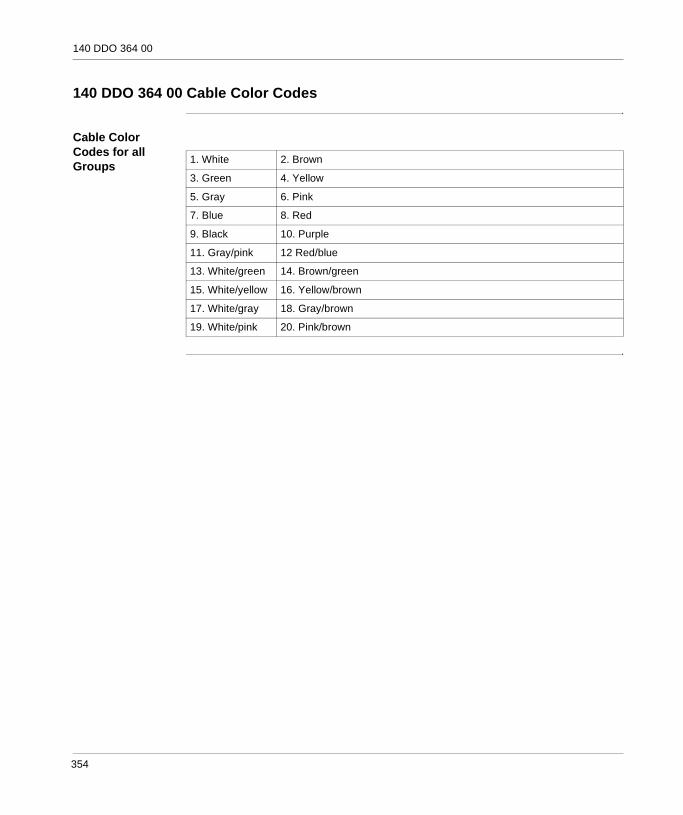
140 DDO 364 00
140 DDO 364 00 Cable Color Codes
Cable Color Codes for all Groups
1. White 2. Brown
3. Green 4. Yellow
5. Gray 6. Pink
7. Blue 8. Red
9. Black 10. Purple
11. Gray/pink 12 Red/blue
13. White/green 14. Brown/green
15. White/yellow 16. Yellow/brown
17. White/gray 18. Gray/brown
19. White/pink 20. Pink/brown
354

140 DDO 364 00
Specifications
General Specifications
General Specifications
Voltage Voltage
Maximum Load Current / Surge Current
Maximum Load Current / Surge Current
Isolation / Protection
Isolation / Protection
Response (Resistive Loads)
Response (Resistive Loads)
Module Type 96 OUT (6 groups x 16 points)
External Power 19.2 ... 30 VDC 19.2 A max. (depends on load)
Power Dissipation 7.0 W
Bus Current required (Module) 250 mA (max.)
I/O map 6 output word
Fault Detection Group indication about loss of field power, faulted point (short circuit or overload
Operating Voltage (max.) 19.2 ... 30 VDC
ON State Drop / Point 0.5 VDC @ 0.5 A
Each Point 0.5 A
Each Group 3.2 A
Per Module 19.2 A
Surge Current (max.) 2 A each point (internally limited)
OFF State Leakage / Point < 1 mA @ 24 VDC
Output to Bus 500 VAC rms for 1 minute
Output Protection (internal) Thermal overload and short circuit
OFF - ON < 1 ms
ON - OFF < 1 ms
355

140 DDO 364 00
Load Inductance / Capacitance (max.)
Load Inductance / Capacitance (max.)
Fuses Fuses
Load Inductance (max.)
0.5 Henry @ 4 Hz switch frequency, or:
Load Capacitance (max.)
50 μF
L = 0.5
l2 F
where: L = Load inductance (henry) l = Load current (A)
F = Switching Frequency (Hz)
Internal -
External User discretion for field power
356

140 DDO 364 00
140 DDO 364 00 Parameter Configuration
Parameter Configuration Window
Parameter and Default Values
DC Output 24V DC 6x16 source
ConfigParameter Name Value
MAPPING DiscreteOUTPUTS STARTING ADDRESS 1OUTPUTS ENDING ADDRESS 96
OUTPUT TYPE BINARY
1 : Local Qu... 2 : 140 DDO.
TIMEOUT STATE USER DEFINEDVALUE 1VALUE 2
TASK MAST
VALUE 3VALUE 4VALUE 5VALUE 6
000000
Name Default Value Options Description
Mapping Discrete WORD (%QW-4X)
Outputs Starting Address 1 1
Outputs Ending Address 96 6
Output Type BINARY BCD
Task(Grayed if module in other than local)
MAST FASTAUX0AUX1AUX2AUX3
fixed to MAST if module in other than local
Timeout State USER DEFINED
HOLD LAST VALUE
Value 1, Value 2,... 0 0-65535 only enabled if Timeout State=USER DEFINED
357

140 DDO 364 00
358

36
140 DDO 843 00: 10 ... 60 VDC 2x8 Source OUT ModuleOverview
Purpose The following chapter provides information of the Quantum 140 DDO 843 00 Module.
What's in this Chapter?
This chapter contains the following topics:
Topic Page
Presentation 360
Indicators 361
Wiring Diagram 362
Specifications 363
Maintenance 364
140 DDO 843 00 Parameter Configuration 365
359

140 DDO 843 00
Presentation
Function The DC Output 10 ... 60 VDC 2x8 Source module switches 10 ... 60 VDC powered loads and is for use with sink devices. External power supplies may be mixed between groups.
Illustration The following figure shows the 140 DDO 843 00 module and its components.
1 Model Number, Module Description, Color Code
2 LED Display
3 Fuse Cutouts
4 Field Wiring Terminal Strip
5 Removable Door
6 Customer Identification Label (Fold label and place it inside door)
Note: The field wiring terminal strip (Modicon #140 XTS 002 00) must be ordered separately. (The terminal strip includes the removable door and label.)
140DDO 843 00
X X
XXXXXXXXXXXXXXXXXXXX
XXXXXXXXXXXXXXXXXXXXX
23
6
8
10
1214
16
18
20
21
232527
29
31
3335
37
1
4
7
9
11
13
1517
19
22
24
26
28
30
32
34
3638
1
2
3
4 5
6
360

140 DDO 843 00
Indicators
Illustration The following table shows the LED indicators for the 140 DDO 843 00 module.
Descriptions The following table shows the LED descriptions for the 140 DDO 843 00 module.
Active F
91102113
1245678
13141516
123
45678
91011
1213141516
LEDs Color Indication when ON
Active Green Bus communication is present.
F Red A fault (external to the module) has been detected.
1 ... 16 Green The indicated point or channel is turned ON.
1 ... 16 Red There is a fault on the indicated point or channel.
361

140 DDO 843 00
Wiring Diagram
Illustration The following figure shows the 140 DDO 843 00 wiring diagram.
Note: N / C = Not Connected
Note: When field wiring the I/O module, the maximum wire size that should be used is 1-14 AWG or 2-16 AWG; the minimum size is 20 AWG.
-
2
10
4
6
8
12
14
16
18
20
22
24
26
28
30 29
27
25
23
21
19
17
15
13
11
9
7
5
3
1+
2 A
2 A
GROUP A SUPPLY
OUTPUT 6
OUTPUT 7
OUTPUT 8
GROUP A COMMON
OUTPUT 9
OUTPUT 10
OUTPUT 11
OUTPUT 12
OUTPUT 3
OUTPUT 1
OUTPUT 2
OUTPUT 4
OUTPUT 5
GROUP B SUPPLY
N/C
N/C
N/C
N/C
N/C
N/C
N/C
N/C
N/C
N/C
N/C
N/C
N/C
N/C
N/C
362

140 DDO 843 00
Specifications
General Specifications
General Specifications
Voltage Voltage
Maximum Load Current / Surge Current
Maximum Load Current / Surge Current
Isolation / Protection
Isolation / Protection
Response (Resistive Loads)
Response (Resistive Loads)
Module Type 16 OUT (2 groups x 8 points)
Logic True High
External Power 10 ... 60 VDC
Power Dissipation 1.0 W + 1 V x Total module load Current
Bus Current required (Module) 160 mA (max.)
I/O map 1 output word
Operating Voltage (max.) 10.2 ... 72 VDC
Absolute Maximum Voltage 72 VDC (continuous)
ON State Drop / Point 1 VDC @ 2 A
Each Point 2 A
Each Group 6 A
Per Module 12 A
Surge Current (max.) 7.5 A @ 50 ms duration (no more than 20 per minute) each point
OFF State Leakage / Point 1 mA @ 60 VDC
Group to Group 700 VAC rms for 1 minute
Group to Bus 2500 VAC rms for 1 minute
Output Protection (internal) Over voltage (suppression diode)
OFF - ON 1 ms
ON - OFF 1 ms
363

140 DDO 843 00
Maintenance
Fuses Fuses
Illustration The following figure shows fuse locations for the 140 DDO 843 00 module.
Internal 8A fuse time-lag for each group (Part # 042701994 or equivalent).
External Each group is protected with an 8 A fuse to protect the module from catastrophic failure. The group fuse is not guaranteed to protect each output switch for all possible overload conditions. It is recommended that each point be fused with a 2 A fuse: Modicon Fuse #: 57-0060-00
CAUTIONPossible danger to equipment or personnel.Turn off power to the module and remove the field wiring terminal strip to gain access to fuses.Failure to follow this precaution can result in injury or equipment damage.
140DDO 353 00
X
Fuse LocationsPoints
1-8
Points9-16
364

140 DDO 843 00
140 DDO 843 00 Parameter Configuration
Parameter Configuration Window
Parameter and Default Values
DC OUT 10-60V 2x8
ConfigParameter Name Value
MAPPING BIT (%M-0X)OUTPUTS STARTING ADDRESS 1OUTPUTS ENDING ADDRESS 16
OUTPUT TYPE BINARY
1 : Local Qu... 2 : 140 DAO.
TIMEOUT STATE USER DEFINEDVALUE
TASK MAST
0
Name Default Value Options Description
Mapping BIT (%M-0x) WORD (%MW-4X)
Outputs Starting Address
1 1
Outputs Ending Address
16 1
Task(Grayed if module in other than local)
MAST FASTAUX0AUX1AUX2AUX3
fixed to MAST if module in other than local
Output Type BINARY BCD
Timeout State USER DEFINED HOLD LAST VALUE
Value 0 0-65535 only enabled if Timeout State=USER DEFINED
365

140 DDO 843 00
366

37
140 DDO 885 00: 24 ... 125 VDC 2x6 Source OUT ModuleOverview
Purpose The following chapter provides information of the Quantum 140 DDO 885 00 Module.
What's in this Chapter?
This chapter contains the following topics:
Topic Page
Presentation 368
Indicators 369
Wiring Diagram 370
Specifications 372
Maintenance 375
140 DDO 885 00 Parameter Configuration 376
367
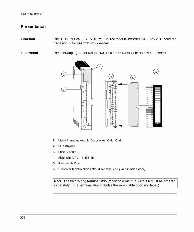
140 DDO 885 00
Presentation
Function The DC Output 24 ... 125 VDC 2x6 Source module switches 24 ... 125 VDC powered loads and is for use with sink devices.
Illustration The following figure shows the 140 DDO 885 00 module and its components.
1 Model Number, Module Description, Color Code
2 LED Display
3 Fuse Cutouts
4 Field Wiring Terminal Strip
5 Removable Door
6 Customer Identification Label (Fold label and place it inside door)
Note: The field wiring terminal strip (Modicon #140 XTS 002 00) must be ordered separately. (The terminal strip includes the removable door and label.)
140DDO 885 00
X X
XXXXXXXXXXXXXXXXXXXX
XXXXXXXXXXXXXXXXXXXXX
23
6
8
10
1214
16
18
20
21
232527
29
31
3335
37
1
4
7
9
11
13
1517
19
22
24
26
28
30
32
34
3638
1
2
3
4 5
6
368

140 DDO 885 00
Indicators
Illustration The following table shows the LED indicators for the 140 DDO 885 00 module with fault indication.
Descriptions The following table shows the LED descriptions for the 140 DDO 885 00 module
Active F
9 1110 2211 3312 44
9101112
5678
5678
LEDs Color Indication when ON
Active Green Bus communication is present.
F Red An over current condition on any point has been detected.
1 ... 12 Green The indicated point or channel is turned ON.
1 ... 12 Red The indicated output point has an over current condition.
Note: To clear a fault, the point must be commanded OFF in user logic.
369

140 DDO 885 00
Wiring Diagram
Illustration The following figure shows the 140 DDO 885 00 wiring diagram.
-2
10
4
6
8
12
14
16
18
20
22
24
26
28
30
32
34
36
38
40 39
37
35
33
31
29
27
25
23
21
19
17
15
13
11
9
7
5
3
1+
OUTPUT 9
OUTPUT 10FIELD
DEVICE
+ -
GROUP A RETURN
OUTPUT 1
N/C
OUTPUT2
OUTPUT 3
OUTPUT 4
N/C
OUTPUT 5
OUTPUT 6
OUTPUT 7
N/C
N/C
OUTPUT 8
GROUP B RETURN
N/C
OUTPUT 11
OUTPUT 12
N/CN/C
GROUP B SUPPLY
GROUP A SUPPLY
N/C
N/C
N/C
N/C
N/C
N/C
N/C
N/C
N/C
N/C
N/C
N/C
N/C
N/C
N/C
N/C
N/C
GROUP A
GROUP B
370

140 DDO 885 00
CAUTIONReverse Polarity PossibilityThis module is not protected against reverse polarity. If you want to protect against polarity miswiring, an external diode in series with each group supply line is recommended. This diode must be able to support the group load current.Failure to follow this precaution can result in injury or equipment damage.
Note: N / C = Not Connected.
Note: When field wiring the I/O module, the maximum wire size that should be used is 1-14 AWG or 2-16 AWG; the minimum size is 20 AWG.
371

140 DDO 885 00
Specifications
General Specifications
General Specifications
Voltage Voltage
Maximum Load Current / Surge Current
Maximum Load Current / Surge Current
Module Type 12 OUT (2 groups x 6 points)
External Power None
Power Dissipation 1.0 W + 0.77 W x points ON
Bus Current required 6 points ON: 375 mA12 points ON: 650 mA
I/O map 1 input word1 output word
Fault Detection Over Current (see note below)
Operating Voltage (max.) 19.2 ... 156.2 VDC including ripple
ON State Drop / Point 0.75 VDC @ 0.5 A
Each Point 0.75 A < 40 degrees C (see the operating curve)
Each Group 3 A, 0 ... 60 degrees C
Per Module 6 A, 0 ... 60 degrees C
Surge Current (max.) 4 A @1 ms duration (no more than 6 per minute)
OFF State Leakage / Point 0.5 mA @ 150 VDC
372

140 DDO 885 00
The following figure shows the 140 DDO 885 00 Output Point Operating Curve.
NOTE: Each group: 3 A, 0 ... 60 degrees C. Per module: 6 A, 0 ... 60 degrees C
Maximum Tungsten
Maximum Tungsten
Inductance and Switching Frequency
Inductance and Switching Frequency
Isolation / Protection
Isolation / Protection
Response (Resistive Loads)
Response (Resistive Loads)
DDO 885 00 Output Point Operating Curve
4030 35 45 50 55 60
0.75
0.625
0.5
AMBIENT TEMPERATURE (deg. C)
OU
TPU
T PO
INT
CU
RR
ENT
(A)
@ 130 VDC 46 W per point
@ 115 VDC 41 W per point
@ 24 VDC 8 W per point
Inductance Internal Diode protected, no limit on Inductance
Switching Frequency 50 Hz (max.)
Field to Bus 2500 VAC rms for 1 minute
Group to Group 1200 VAC rms for 1 minute
Output Protection (internal) Group varistor and individual point over Current sense
OFF - ON 1 ms
ON - OFF 1 ms
373

140 DDO 885 00
Note: Each output point is protected by an over current sense circuit. When an over current condition is detected, the point is turned OFF, its LED fault indicator is turned ON, and the appropriate bit is set in the module fault register.The output point will be turned OFF after a short is detected. A fault greater than 9.4 A will guarantee that the point will be turned OFF and will latch the output point in the OFF state. To clear a fault, the point must be commanded OFF in user logic.
374
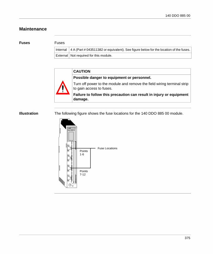
140 DDO 885 00
Maintenance
Fuses Fuses
Illustration The following figure shows the fuse locations for the 140 DDO 885 00 module.
Internal 4 A (Part # 043511382 or equivalent). See figure below for the location of the fuses.
External Not required for this module.
CAUTIONPossible danger to equipment or personnel.Turn off power to the module and remove the field wiring terminal strip to gain access to fuses.Failure to follow this precaution can result in injury or equipment damage.
140DDO 885 00
X
Fuse LocationsPoints1-6
Points7-12
375

140 DDO 885 00
140 DDO 885 00 Parameter Configuration
Parameter Configuration Window
125VDC OUT 2x6
ConfigParameter Name Value
MAPPING BIT (%I-1X%M-0X)
OUTPUTS STARTING ADDRESS
1
OUTPUTS ENDING ADDRESS 16
OUTPUT TYPE BINARY
1 : Local Qu... 2 : 140 DDO.
TIMEOUT STATE USER DEFINEDVALUE
TASK MASTINPUT TYPE
INPUTS STARTING ADDRESSINPUTS ENDING ADDRESS
BINARY
161
0
376

140 DDO 885 00
Parameter and Default Values
Name Default Value Options Description
Mapping BIT (%I-1X%M-0X) WORD (%IW-3X%MW-4X)
Inputs Starting Address
1 1
Inputs Ending Address
16 1
Outputs Starting Address
1 1
Outputs Ending Address
16 1
Task(Grayed if module in other than local)
MAST FASTAUX0AUX1AUX2AUX3
fixed to MAST if module in other than local
Input Type BINARY BCD
Output Type BINARY BCD
Timeout State USER DEFINED HOLD LAST VALUE
Value 0 0-65535 only enabled if Timeout State=USER DEFINED
377

140 DDO 885 00
378

38
140 DAO 840 00: 24 ... 230 VAC 16x1 OUT ModuleOverview
Purpose The following chapter provides information of the Quantum 140 DAO 840 00 Module.
What's in this Chapter?
This chapter contains the following topics:
Topic Page
Presentation 380
Indicators 381
Wiring Diagram 382
Specifications 384
140 DAO 840 00 Parameter Configuration 387
379

140 DAO 840 00
Presentation
Function The AC Output 24 ... 230 VAC 16x1 module switches 24 ... 230 VAC powered loads.
Illustration The following figure shows the 140 DAO 840 00 module and its components.
1 Model Number, Module Description, Color Code
2 LED Display
3 Fuse Cutouts
4 Field Wiring Terminal Strip
5 Removable Door
6 Customer Identification Label (Fold label and place it inside door)
Note: The field wiring terminal strip (Modicon #140 XTS 002 00) must be ordered separately. (The terminal strip includes the removable door and label.)
140DAO 840 00
X X
XXXXXXXXXXXXXXXXXXXX
XXXXXXXXXXXXXXXXXXXXX
23
6
8
10
1214
16
18
20
21
232527
29
31
3335
37
1
4
7
9
11
13
1517
19
22
24
26
28
30
32
34
3638
1
2
3
4 5
6
380

140 DAO 840 00
Indicators
Illustration The following table shows the LED indicators for the 140 DAO 840 00 module.
Descriptions The following table shows the LED descriptions for the 140 DAO 840 00 module.
Active F
91102113
1245678
13141516
123
45678
91011
1213141516
LEDs Color Indication when ON
Active Green Bus communication is present.
F Red A fault (external to the module) has been detected.
1 ... 16 Green The indicated point or channel is turned ON.
1 ... 16 Red There is a fault on the indicated point or channel.
381

140 DAO 840 00
Wiring Diagram
Illustration The following figure shows the 140 DAO 840 00 wiring diagram.
OUTPUT 1 LINE
5 A (see CAUTION 2)
2
10
4
6
8
12
14
16
18
20
22
24
26
28
30
32
34
36
38
40 39
37
35
33
31
29
27
25
23
21
19
17
15
13
11
9
7
5
3
1OUTPUT 2
OUTPUT 3
OUTPUT 4
OUTPUT 5
OUTPUT 6
OUTPUT 7
OUTPUT 8
OUTPUT 9
OUTPUT 10
OUTPUT 11
OUTPUT 12
OUTPUT 13
OUTPUT 14
OUTPUT 15
OUTPUT 16
N/C N/C
N/C
N/C
N/C
N/C
N/C
N/C
L N
OUTPUT 2 LINE
OUTPUT 3 LINE
OUTPUT 4 LINE
OUTPUT 5 LINE
OUTPUT 6 LINE
OUTPUT 7 LINE
OUTPUT 8 LINE
OUTPUT 9 LINE
OUTPUT 10 LINE
OUTPUT 11 LINE
OUTPUT 12 LINE
OUTPUT 13 LINE
OUTPUT 14 LINE
OUTPUT 15 LINE
OUTPUT 16 LINE
382

140 DAO 840 00
1. This module is not polarity sensitive.2. N / C = Not Connected.3. Voltages up to 133V may be different phases on adjacent output points.4. Voltages over 133V of different phases must have an output point separation between them. For example: Output 1 and 2 - Phase A, Skip Output 3, Output 4 - Phase B5. When field wiring the I/O module, the maximum wire size that should be used is 1-14 AWG or 2-16 AWG; the minimum size is 20 AWG.
CAUTIONElectrical Shock hazardTurn off power to the module and remove the field wiring terminal strip to gain access to fuses.Failure to follow this precaution can result in injury or equipment damage.
CAUTIONSafety precaution to avoid equipment damageEach output point must be fused with an external fuse. The recommended fuse is a 5 A fuse (Part # 043502405) or any other fuse with an I2T rating of less than 87.Failure to follow this precaution can result in injury or equipment damage.
383

140 DAO 840 00
Specifications
General Specifications
General Specifications
Absolute Maximum Input
Absolute Maximum Input
Voltage Voltage
Maximum Load Current
Maximum Load Current
Module Type 16 OUT isolated
External Power Not required for this module
Power Dissipation 1.85 W + 1.1 V x Total module load Currents
Bus Current required (Module) 350 mA
I/O map 1 output words
10 s 300 VAC
1 Cycle 400 VAC
Operating Voltage (max.) 20 ... 253 VAC
ON State Drop / Point 1.5 VAC
Each Point 4.0 A continuous, 20 ... 132 VAC rms3.0 A continuous, 170 ... 253 VAC rms
Any four contiguous Points
4.0 A max. continuous for the sum of the four points.
Per Module 16 A continuous (see chart below)
384

140 DAO 840 00
The following figure shows the 140 DAO 840 00 operating curve.
Frequency and Minimum Load Current
Frequency and Minimum Load Current
OFF State Leakage / Point (max.)
OFF State Leakage / Point (max.)
Surge Current (max. rms)
Surge Current (max. rms)
1716151413121110 9 8 7 6 5 4 3 2 1
30 35 40 45 50 55 60
20-132 V rms
170-253 V rms
AMBIENT TEMPERATURE ( deg.C)TO
TAL
MO
DU
LE C
UR
REN
T (A
)
*The specifications stated are pending UL/CSA approval. This module was originallyapproved at 2 A each point; and 12 A, 0 ... 50° C (115 VAC) and 0 ... 50° C (230 VAC)per module.
Frequency 47 ... 63 Hz
Minimum Load Current 5 mA
OFF State Leakage / Point (max.) 2.5 mA @ 230 VAC2 mA @ 115 VAC1 mA @ 48 VAC1 mA @ 24 VAC
One Cycle 30 A per point
Two Cycles 20 A per point
Three Cycles 10 A per point
Applied DV/DT 400 V / μs
385

140 DAO 840 00
Isolation / Protection
Isolation / Protection
Response Response
Fuses Fuses
Output to Output 1500 VAC rms for 1 minute
Output to Bus 1780 VAC rms for 1 minute
Output Protection (internal) RC snubber suppression
OFF - ON 0.5 of one line cycle max.
ON - OFF 0.5 of one line cycle max.
Internal None
External Each output point must be fused with an external fuse . The recommended fuse is a 5 A fuse (Part # 043502405 or equivalent) or any of he fuse with an I2T rating of less than 87.
386

140 DAO 840 00
140 DAO 840 00 Parameter Configuration
Parameter Configuration Window
Parameter and Default Values
AC OUT 24-230 16x1
Config
Parameter Name ValueMAPPING BIT (%M-0X)OUTPUTS STARTING ADDRESS 1OUTPUTS ENDING ADDRESS 16
OUTPUT TYPE BINARY
1 : Local Qu... 2 : 140 DAO.
TIMEOUT STATE USER DEFINEDVALUE
TASK MAST
0
Name Default Value Options Description
Mapping BIT (%M-0x) WORD (%MW-4X)
Output Starting Address 1 1
Output Ending Address 16 1
Output Type BINARY BCD
Task(Grayed if module in other than local)
MAST FASTAUX0AUX1AUX2AUX3
fixed to MAST if module in other than local
Timeout State USERDEFINED HOLD LAST VALUE
Value 0 0-65535 only enabled if Timeout State=USERDEFINED
387

140 DAO 840 00
388

39
140 DAO 840 10: 24 ... 115 VAC 16x1 OUT ModuleOverview
Purpose The following chapter provides information of the Quantum 140 DAO 840 10 Module.
What's in this Chapter?
This chapter contains the following topics:
Topic Page
Presentation 390
Indicators 391
Wiring Diagram 392
Specifications 394
140 DAO 840 10 Parameter Configuration 397
389

140 DAO 840 10
Presentation
Function The AC Output 24 ... 115 VAC 16x1 module switches 24 ... 115 VAC powered loads.
Illustration The following figure shows the 140 DAO 840 10 module and its components.
1 Model Number, Module Description, Color Code
2 LED Display
3 Fuse Cutouts
4 Field Wiring Terminal Strip
5 Removable Door
6 Customer Identification Label (Fold label and place it inside door)
Note: The field wiring terminal strip (Modicon #140 XTS 002 00) must be ordered separately. (The terminal strip includes the removable door and label.)
140DAO 840 10
X X
XXXXXXXXXXXXXXXXXXXX
XXXXXXXXXXXXXXXXXXXXX
23
6
8
10
1214
16
18
20
21
232527
29
31
3335
37
1
4
7
9
11
13
1517
19
22
24
26
28
30
32
34
3638
1
2
3
4 5
6
390

140 DAO 840 10
Indicators
Illustration The following table shows the LED indicators for the 140 DAO 840 10 module.
Descriptions The following table shows the LED descriptions for the 140 DAO 840 10 module.
Active F
91102113
1245678
13141516
123
45678
91011
1213141516
LEDs Color Indication when ON
Active Green Bus communication is present.
F Red A fault (external to the module) has been detected.
1 ... 16 Green The indicated point or channel is turned ON.
1 ... 16 Red There is a fault on the indicated point or channel.
391
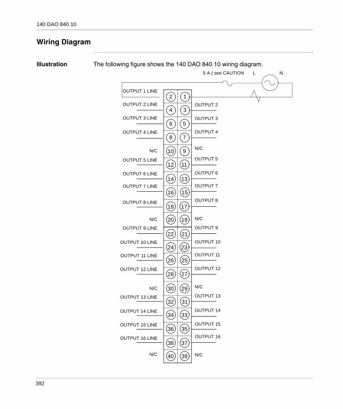
140 DAO 840 10
Wiring Diagram
Illustration The following figure shows the 140 DAO 840 10 wiring diagram.
OUTPUT 1 LINE
5 A ( see CAUTION
2
10
4
6
8
12
14
16
18
20
22
24
26
28
30
32
34
36
38
40 39
37
35
33
31
29
27
25
23
21
19
17
15
13
11
9
7
5
3
1OUTPUT 2
OUTPUT 3
OUTPUT 4
OUTPUT 5
OUTPUT 6
OUTPUT 7
OUTPUT 8
OUTPUT 9
OUTPUT 10
OUTPUT 11
OUTPUT 12
OUTPUT 13
OUTPUT 14
OUTPUT 15
OUTPUT 16
N/C N/C
N/C
N/C
N/C
N/C
N/C
N/C
L N
OUTPUT 2 LINE
OUTPUT 3 LINE
OUTPUT 4 LINE
OUTPUT 5 LINE
OUTPUT 6 LINE
OUTPUT 7 LINE
OUTPUT 8 LINE
OUTPUT 9 LINE
OUTPUT 10 LINE
OUTPUT 11 LINE
OUTPUT 12 LINE
OUTPUT 13 LINE
OUTPUT 14 LINE
OUTPUT 15 LINE
OUTPUT 16 LINE
392

140 DAO 840 10
CAUTIONElectrical Shock hazardEach output point must be fused with an external fuse. The recommended fuse is a 5 A fuse (Part # 043502405), or any other fuse with an I2T rating of less than 87.Failure to follow this precaution can result in injury or equipment damage.
CAUTIONSafety precaution to avoid equipment damageEach output point must be fused with an external fuse. The recommended fuse is a 5 A fuse (Part # 043502405), or any other fuse with an I2T rating of less than 87.Failure to follow this precaution can result in injury or equipment damage.
Note: This module is not polarity sensitive.N / C = Not Connected
Note: When field wiring the I/O module, the maximum wire size that should be used is 1-14 AWG or 2-16 AWG; the minimum size is 20 AWG.
393
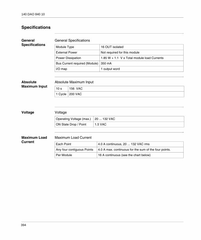
140 DAO 840 10
Specifications
General Specifications
General Specifications
Absolute Maximum Input
Absolute Maximum Input
Voltage Voltage
Maximum Load Current
Maximum Load Current
Module Type 16 OUT isolated
External Power Not required for this module
Power Dissipation 1.85 W + 1.1 V x Total module load Currents
Bus Current required (Module) 350 mA
I/O map 1 output word
10 s 156 VAC
1 Cycle 200 VAC
Operating Voltage (max.) 20 ... 132 VAC
ON State Drop / Point 1.5 VAC
Each Point 4.0 A continuous, 20 ... 132 VAC rms
Any four contiguous Points 4.0 A max. continuous for the sum of the four points.
Per Module 16 A continuous (see the chart below)
394

140 DAO 840 10
The following figure shows the 140 DAO 840 10 operating curve.
Frequency and Minimum Load Current
OFF State Leakage / Point (max.)
OFF State Leakage / Point (max.)
Surge Current (max. rms)
Surge Current (max. rms)
1716151413121110 9 8 7 6 5 4 3 2 1
30 35 40 45 50 55 60
20-132 V rms
TOTA
L M
OD
ULE
CU
RR
ENT
(A)
DAO 840 10 Operating Curve*
Frequency 47 ... 63 Hz
Minimum Load Current 5 mA
OFF State Leakage / Point (max.) 2.5 mA @ 230 VAC2 mA @ 115 VAC1 mA @ 48 VAC1 mA @ 24 VAC
One Cycle 30 A per point
Two Cycles 20 A per point
Three Cycles 10 A per point
Applied dV/dT 400 V / μs
395

140 DAO 840 10
Isolation / Protection
Isolation / Protection
Response Response
Fuses Fuses
Output to Output 1500 VAC rms for 1 minute
Output to Bus 1780 VAC rms for 1 minute
Output Protection (internal) RC snubber suppression
OFF - ON 0.5 of one line cycle max.
ON - OFF 0.5 of one line cycle max.
Internal None
External Each output point must be fused with an external fuse . The recommended fuse is a 5 A fuse (Part # 043502405 or equivalent) or any of he fuse with an I2T rating of less than 87.
396

140 DAO 840 10
140 DAO 840 10 Parameter Configuration
Parameter Configuration Window
Parameter and Default Values
AC OUT 24-115V 16x1
Config
Parameter Name ValueMAPPING BIT (%M-0X)OUTPUTS STARTING ADDRESS 1OUTPUTS ENDING ADDRESS 16
OUTPUT TYPE BINARY
1 : Local Qu... 2 : 140 DAO.
TIMEOUT STATE USER DEFINEDVALUE
TASK MAST
0
Name Default Value Options Description
Mapping BIT (%M-0x) WORD (%MW-4X)
Output Starting Address 1 1
Output Ending Address 16 1
Task(Grayed if module in other than local)
MAST FASTAUX0AUX1AUX2AUX3
fixed to MAST if module in other than local
Output Type BINARY BCD
Timeout State USER DEFINED
HOLD LAST VALUE
Value 0 0-65535 only enabled if Timeout State=USER DEFINED
397

140 DAO 840 10
398

40
140 DAO 842 10: 100 ... 230 VAC 4x4 OUT ModuleOverview
Purpose The following chapter provides information of the Quantum 140 DAO 842 10 Module.
What's in this Chapter?
This chapter contains the following topics:
Topic Page
Presentation 400
Indicators 401
Wiring Diagram 402
Specifications 404
Maintenance 407
140 DAO 842 10 Parameter Configuration 408
399

140 DAO 842 10
Presentation
Function The AC Output 100 ... 230 VAC 4x4 module switches 100 ... 230 VAC powered loads.
Illustration The following figure shows the 140 DAO 842 10 module and its components.
1 Model Number, Module Description, Color Code
2 LED Display
3 Fuse Cutouts
4 Field Wiring Terminal Strip
5 Removable Door
6 Customer Identification Label (Fold label and place it inside door)
Note: The field wiring terminal strip (Modicon #140 XTS 002 00) must be ordered separately. (The terminal strip includes the removable door and label.)
140DAO 842 10
X X
XXXXXXXXXXXXXXXXXXXX
XXXXXXXXXXXXXXXXXXXXX
23
6
8
10
1214
16
18
20
21
232527
29
31
3335
37
1
4
7
9
11
13
1517
19
22
24
26
28
30
32
34
3638
1
2
3
4 5
6
400

140 DAO 842 10
Indicators
Illustration The following table shows the LED indicators for the 140 DAO 842 10 module.
Descriptions The following table shows the LED descriptions for the 140 DAO 842 10 module.
Active F
91102113
124
5678
13141516
LEDs Color Indication when ON
Active Green Bus communication is present.
F Red A fault (external to the module) has been detected.
1 ... 16 Green The indicated point or channel is turned ON.
1 ... 45 ... 89 ... 1213 ... 16
Red The indicated group has a blown fuse or no field power.
401

140 DAO 842 10
Wiring Diagram
Illustration The following figure shows the wiring diagram for the 140 DAO 842 10 module.
OUTPUT
OUTPUT
OUTPUT
OUTPUT
GROUP B COMMON
GROUP D COMMON
OUTPUT
N/C
N/C
N/C
N/C
N/C
N/C
N/C
N/C
GROUP A HOT
GROUP C COMMON
OUTPUT
OUTPUT
OUTPUT
2
10
4
6
8
12
14
16
18
20
22
24
26
28
30
32
34
36
38
40 39
37
35
33
31
29
27
25
23
21
19
17
15
13
11
9
7
5
3
1
GROUP A COMMON
L
GROUP B HOT
N/C
N/C
N/C
N/C
GROUP C HOT
GROUP D HOT
N/C
N/C
N/C
N/C
OUTPUT
OUTPUT 10
OUTPUT 11
OUTPUT 13
OUTPUT 14
OUTPUT 15
OUTPUT 12
OUTPUT 16
Optional Fuse
N
402

140 DAO 842 10
CAUTIONPower CompatibilityThe AC power energizing each group must be from a common, single-phase AC power source.Failure to follow this precaution can result in injury or equipment damage.
CAUTIONWiring CompatibilityIf an external switch is wired to control an inductive load in parallel with the module output, then an external varistor (Harris V390ZA05 or equivalent) must be wired in parallel with the switch.Failure to follow this precaution can result in injury or equipment damage.
Note: 1. This module is not polarity sensitive.N / C = Not Connected
Note: When field wiring the I/O module, the maximum wire size that should be used is 1-14 AWG or 2-16 AWG; the minimum size is 20 AWG.
403

140 DAO 842 10
Specifications
General Specifications
General Specifications
Absolute Maximum Input
Absolute Maximum Input
Voltage Voltage
Maximum Load Current
Maximum Load Current
Module Type 16 OUT (4 groups x 4 points)
External Power 85 ... 253 VAC
Power Dissipation 1.85 W + 1.1 V x Total module load Currents
Bus Current required (Module) 350 mA
I/O map 1 output words
Fault Detection Blown fuse detect, loss of field power
10 s 300 VAC
1 Cycle 400 VAC
Operating Voltage (max.) 85 ... 253 VAC
ON State Drop / Point 1.5 VAC
Each Point 4.0 A continuous, 85 ... 132 VAC rms3.0 A continuous, 170 ... 253 VAC rms
Each Group 4.0 A continuous
Per Module 16 A continuous (see the chart below)
404

140 DAO 842 10
The following figure shows the 140 DAO 842 10 Operating Curve.
Frequency and Minimum Load Current
OFF State Leakage / Point (max.)
OFF State Leakage / Point (max.)
Surge Current (max. rms)
Surge Current (max. rms)
1716151413121110 9 8 7 6 5 4 3 2 1
30 35 40 45 50 55 60
20-132 V rms
170-253 V rms
AMBIENT TEMPERATURE ( deg. C)
TOTA
L M
OD
ULE
CU
RR
ENT
(A)
DAO 842 10 Operating Curve*
*The specifications stated are pending UL/CSA approval. This module was originally approved at 2 Aeach point; and 12 A, 0 ... 50° C (115 VAC) and 0 ... 50° C (230 VAC) per module.
Frequency 47 ... 63 Hz
Minimum Load Current 5 mA
OFF State Leakage / Point (max.) 2.5 mA @ 230 VAC2 mA @ 115 VAC
One Cycle 30 A per point, 45 A per group
Two Cycles 20 A per point, 30 A per group
Three Cycles 10 A per point, 25 A per group
Applied dV/dT 400 V / μs
405

140 DAO 842 10
Isolation / Protection
Isolation / Protection
Response Response
Group to Group 1000 VAC rms for 1 minute, galvanically isolated
Output to Bus 1780 VAC rms for 1 minute
Output Protection (internal) RC snubber suppression
OFF - ON 0.5 of one line cycle max.
ON - OFF 0.5 of one line cycle max.
406

140 DAO 842 10
Maintenance
Fuses Fuses
Illustration The following figure shows the fuse locations for the DAO 842 10 module.
Internal None
External Each output point must be fused with an external fuse. The recommended fuse is
a 5 A fuse (Part # 043502405 or equivalent) or any other fuse with an T rating
of less than 87.
WARNINGPossible injury to personnel or equipmentFirst turn off the power to the module to remove the field wiring terminal strip to gain access to the fuses.Failure to follow this precaution can result in death, serious injury, or equipment damage.
I2
140DDO 842 10
X
Fuse LocationsPoints
1-4
Points5-8
Points9-12
Points13-16
407

140 DAO 842 10
140 DAO 842 10 Parameter Configuration
Parameter Configuration Window
Parameter and Default Values
AC OUT 100-230V 4x4
Config
Parameter Name ValueMAPPING BIT (%M-0X)OUTPUTS STARTING ADDRESS 1OUTPUTS ENDING ADDRESS 16
OUTPUT TYPE BINARY
1 : Local Qu... 2 : 140 DAO.
TIMEOUT STATE USER DEFINEDVALUE
TASK MAST
0
Name Default Value Options Description
Mapping BIT (%M-0x) WORD (%MW-4X)
Outputs Starting Address 1 1
Outputs Ending Address 16 1
Task(Grayed if module in other than local)
MAST FASTAUX0AUX1AUX2AUX3
fixed to MAST if module in other than local
Output Type BINARY BCD
Timeout State USER DEFINED
HOLD LAST VALUE
Value 0 0-65535 only enabled if Timeout State=USER DEFINED
408

41
140 DAO 842 20: 24 ... 48 VAC 4x4 OUT ModuleOverview
Purpose The following chapter provides information of the Quantum 140 DAO 842 20 Module.
What's in this Chapter?
This chapter contains the following topics:
Topic Page
Presentation 410
Indicators 411
Wiring Diagram 412
Specifications 414
Maintenance 417
140 DAO 842 20 Parameter Configuration 418
409
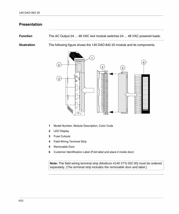
140 DAO 842 20
Presentation
Function The AC Output 24 ... 48 VAC 4x4 module switches 24 ... 48 VAC powered loads.
Illustration The following figure shows the 140 DAO 842 20 module and its components.
1 Model Number, Module Description, Color Code
2 LED Display
3 Fuse Cutouts
4 Field Wiring Terminal Strip
5 Removable Door
6 Customer Identification Label (Fold label and place it inside door)
Note: The field wiring terminal strip (Modicon #140 XTS 002 00) must be ordered separately. (The terminal strip includes the removable door and label.)
140DAO 842 20
X X
XXXXXXXXXXXXXXXXXXXX
XXXXXXXXXXXXXXXXXXXXX
23
6
8
10
1214
16
18
20
21
232527
29
31
3335
37
1
4
7
9
11
13
1517
19
22
24
26
28
30
32
34
3638
1
2
3
4 5
6
410

140 DAO 842 20
Indicators
Illustration The following table shows the LED indicators for the 140 DAO 842 20 module.
Descriptions The following table shows the LED descriptions for the 140 DAO 842 20 module.
Active F
91102113
124
5678
13141516
LEDs Color Indication when ON
Active Green Bus communication is present.
F Red A fault (external to the module) has been detected.
1 ... 16 Green The indicated point or channel is turned ON.
1 ... 45 ... 89 ... 1213 ... 16
Red The indicated group has a blown fuse or no field power.
411
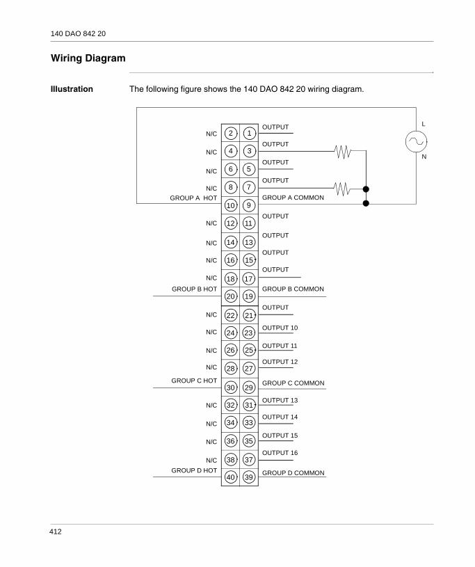
140 DAO 842 20
Wiring Diagram
Illustration The following figure shows the 140 DAO 842 20 wiring diagram.
OUTPUT
OUTPUT
OUTPUT
OUTPUT
GROUP B COMMON
GROUP D COMMON
OUTPUT
N/C
N/C
N/C
N/C
N/C
N/C
N/C
N/C
GROUP A HOT
GROUP C COMMON
OUTPUT
OUTPUT
OUTPUT
2
10
4
6
8
12
14
16
18
20
22
24
26
28
30
32
34
36
38
40 39
37
35
33
31
29
27
25
23
21
19
17
15
13
11
9
7
5
3
1
GROUP A COMMON
L
GROUP B HOT
N/C
N/C
N/C
N/C
GROUP C HOT
GROUP D HOT
N/C
N/C
N/C
N/C
OUTPUT
OUTPUT 10
OUTPUT 11
OUTPUT 13
OUTPUT 14
OUTPUT 15
OUTPUT 12
OUTPUT 16
N
412

140 DAO 842 20
CAUTIONPower CompatibilityThe AC power energizing each group must be from a common, single-phase AC power source.Failure to follow this precaution can result in injury or equipment damage.
CAUTIONWiring CompatibilityIf an external switch is wired to control an inductive load in parallel with the module output, then an external varistor (Harris V390ZA05 or equivalent) must be wired in parallel with the switch.Failure to follow this precaution can result in injury or equipment damage.
Note: 1. This module is not polarity sensitive.N / C = Not Connected
Note: When field wiring the I/O module, the maximum wire size that should be used is 1-14 AWG or 2-16 AWG; the minimum size is 20 AWG.
413

140 DAO 842 20
Specifications
General Specifications
General Specifications
Absolute Maximum Input
Absolute Maximum Input
Voltage Voltage
Maximum Load Current
Maximum Load Current
Module Type 16 OUT (4 groups x 4 points)
External Power 20 ... 56 VAC
Power Dissipation 1.85 W + 1.1 V x Total module load Currents
Bus Current required (Module) 350 mA
I/O map 1 output words
Fault Detection Blown fuse detect, loss of field power
10 s 63 VAC
1 Cycle 100 VAC
1.3 ms 111 VAC peak
Operating Voltage (max.) 20 ... 56 VAC
ON State Drop / Point 1.5 VAC
Each Point 4.0 A continuous, 20 ... 56 VAC rms
Each Group 4.0 A continuous
Per Module 16 A continuous (see the chart below)
414
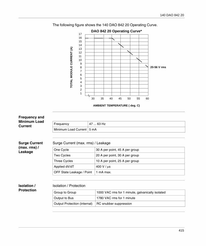
140 DAO 842 20
The following figure shows the 140 DAO 842 20 Operating Curve.
Frequency and Minimum Load Current
Surge Current (max. rms) / Leakage
Surge Current (max. rms) / Leakage
Isolation / Protection
Isolation / Protection
1716151413121110 9 8 7 6 5 4 3 2 1
30 35 40 45 50 55 60
20-56 V rms
AMBIENT TEMPERATURE ( deg. C)
TOTA
L M
OD
ULE
CU
RR
ENT
(A)
DAO 842 20 Operating Curve*
Frequency 47 ... 63 Hz
Minimum Load Current 5 mA
One Cycle 30 A per point, 45 A per group
Two Cycles 20 A per point, 30 A per group
Three Cycles 10 A per point, 25 A per group
Applied dV/dT 400 V / μs
OFF State Leakage / Point 1 mA max.
Group to Group 1000 VAC rms for 1 minute, galvanically isolated
Output to Bus 1780 VAC rms for 1 minute
Output Protection (internal) RC snubber suppression
415

140 DAO 842 20
Response Response
OFF - ON 0.5 of one line cycle max.
ON - OFF 0.5 of one line cycle max.
416

140 DAO 842 20
Maintenance
Fuses Fuses
Illustration The following figure shows the 140 DAO 842 20 fuse locations.
Internal 5 A fuse for each group. (Part # 043502405 or equivalent). For the location of the fuses see the figure below.
External User Discretion
WARNINGPossible injury to personnel or equipmentFirst turn off the power to the module to remove the field wiring terminal strip to gain access to the fuses.Failure to follow this precaution can result in death, serious injury, or equipment damage.
140DDO 842 20
X
Fuse LocationsPoints
1-4
Points5-8
Points9-12
Points13-16
417

140 DAO 842 20
140 DAO 842 20 Parameter Configuration
Parameter Configuration Window
Parameter and Default Values
AC OUT 24-48V 4x4
Config
Parameter Name ValueMAPPING BIT (%M-0X)OUTPUTS STARTING ADDRESS 1OUTPUTS ENDING ADDRESS 16
OUTPUT TYPE BINARY
1 : Local Qu... 2 : 140 DAO.
TIMEOUT STATE USER DEFINEDVALUE
TASK MAST
0
Name Default Value Options Description
Mapping BIT (%M-0x) WORD (%MW-4X)
Outputs Starting Address
1 1
Outputs Ending Address
16 1
Task(Grayed if module in other than local)
MAST FASTAUX0AUX1AUX2AUX3
fixed to MAST if module in other than local
Output Type BINARY BCD
Timeout State USER DEFINED HOLD LAST VALUE
Value 0 0-65535 only enabled if Timeout State=USER DEFINED
418

42
140 DAO 853 00: 230 VAC 4x8 Source OUT ModuleOverview
Purpose The following chapter provides information of the Quantum 140 DAO 853 00 Module.
What's in this Chapter?
This chapter contains the following topics:
Topic Page
Presentation 420
Indicators 421
Wiring Diagram 422
Specifications 424
Maintenance 427
140 DAO 853 00 Parameter Configuration 428
419

140 DAO 853 00
Presentation
Function The AC Output 230 VAC 4x8 module accepts 230 VAC powered loads.
Illustration The following figure shows the 140 DAO 853 00 module and its components.
1 Model Number, Module Description, Color Code
2 LED Display
3 Fuse Cutouts
4 Field Wiring Terminal Strip
5 Removable Door
6 Customer Identification Label (Fold label and place it inside door)
Note: The field wiring terminal strip (Modicon #140 XTS 002 00) must be ordered separately. (The terminal strip includes the removable door and label.)
140DAO 853 00
X X
XXXXXXXXXXXXXXXXXXXX
XXXXXXXXXXXXXXXXXXXXX
23
6
8
10
1214
16
18
20
21
232527
29
31
3335
37
1
4
7
9
11
13
1517
19
22
24
26
28
30
32
34
3638
1
2
3
4 5
6
420

140 DAO 853 00
Indicators
Illustration The following table shows the LED indicators for the 140 DAO 853 00 module.
Descriptions The following table shows the LED descriptions for the 140 DAO 853 00 modul.
Active F
91102113
1245678
13141516
171819
2021222324
252627
2829303132
LEDs Color Indication when ON
Active Green Bus communication is present.
F Red A fault (external to the module) has been detected.
1 ... 32 Green The indicated point or channel is turned ON.
421

140 DAO 853 00
Wiring Diagram
Illustration The following figure shows the 140 DAO 853 00 wiring diagram.
OUTPUT 1
OUTPUT 3
OUTPUT 5
OUTPUT 7
OUTPUT 15
GROUP A HOT
OUTPUT 13
OUTPUT 11
OUTPUT 9
2
10
4
6
8
12
14
16
18
20
22
24
26
28
30
32
34
36
38
40 39
37
35
33
31
29
27
25
23
21
19
17
15
13
11
9
7
5
3
1
N/C
L
GROUP B HOT
GROUP C HOT
GROUP D HOT
OUTPUT 17
OUTPUT 19
OUTPUT 21
OUTPUT 25
OUTPUT 27
OUTPUT 29
OUTPUT 23
OUTPUT 31
NOUTPUT 2
OUTPUT 4
OUTPUT 6
OUTPUT 8
OUTPUT 10
OUTPUT 12
OUTPUT 14
OUTPUT 16
OUTPUT 18
OUTPUT 20
OUTPUT 22
OUTPUT 24
OUTPUT 26
OUTPUT 28
OUTPUT 30
OUTPUT 32
N/C
N/C
N/C
422

140 DAO 853 00
CAUTIONPower CompatibilityThe AC power energizing each group must be from a common, single-phase AC power source.Failure to follow this precaution can result in injury or equipment damage.
CAUTIONWiring CompatibilityIf an external switch is wired to control an inductive load in parallel with the module output, then an external varistor (Harris V390ZA05 or equivalent) must be wired in parallel with the switch.Failure to follow this precaution can result in injury or equipment damage.
Note: When field wiring the I/O module, the maximum wire size that should be used is 1-14 AWG or 2-16 AWG; the minimum size is 20 AWG.
423

140 DAO 853 00
Specifications
General Specifications
General Specifications
Absolute Maximum Input
Absolute Maximum Input
Voltage Voltage
Maximum Load Current
Maximum Load Current
Module Type 32 OUT (4 groups x 8 points)
Logic True High
External Power Not required for this module
Power Dissipation 1.60 W + 1.0 V x Total module load Currents
Bus Current required (Module) 320 mA
I/O map 2 output words
10 s 300 VAC
1 Cycle 400 VAC
Operating Voltage (max.) 20 ... 253 VAC
ON State Drop / Point 1.5 VAC
Each Point 1.0 A continuous, 20 ... 253 VAC rms
Each Group 4.0 A (max.)
Per Module 16 A continuous (see chart below)
424

140 DAO 853 00
The following figure shows the 140 DAO 853 00 Operating Curve.
Frequency and Minimum Load Current
OFF State Leakage / Point (max.)
OFF State Leakage / Point (max.)
1716151413121110 9 8 7 6 5 4 3 2 1
30 35 40 45 50 55 60
NO POINTEXCEEDS 0.5A
AMBIENT TEMPERATURE ( deg. C)
TOTA
L M
OD
ULE
CU
RR
ENT
(A)
DAO 853 00 Operating Curve*
65
NO POINTEXCEEDS 1.0A
0
Frequency 47 ... 63 Hz
Minimum Load Current 30 mA
OFF State Leakage / Point (max.) 0.88 mA @ 230 VAC0.44 mA @ 115 VAC0.18 mA @ 48 VAC0.09 mA @ 24 VAC
425

140 DAO 853 00
Surge Current (max. rms)
Surge Current (max. rms)
Isolation / Protection
Isolation / Protection
Response Response
One Cycle 30 A per point
Two Cycles 20 A per point
Three Cycles 10 A per point
Applied dV/dT 400 V / μs
Group to Group 1780 VAC rms for 1 minute
Output to Bus 1780 VAC rms for 1 minute
Output Protection (internal) RC snubber protection
OFF - ON 0.5 of one line cycle max.
ON - OFF 0.5 of one line cycle max.
426

140 DAO 853 00
Maintenance
Fuses Fuses
Illustration The following figure shows the fuse locations for the DAO 853 00 module.
Internal 4 A, 250 V fuse (Little fuse 217004) for each group. For location of fuses see below
External User discretion
140DDO 853 00
X
Fuse LocationsPoints
1-8
Points9-16
Points17-24
Points25-32
427
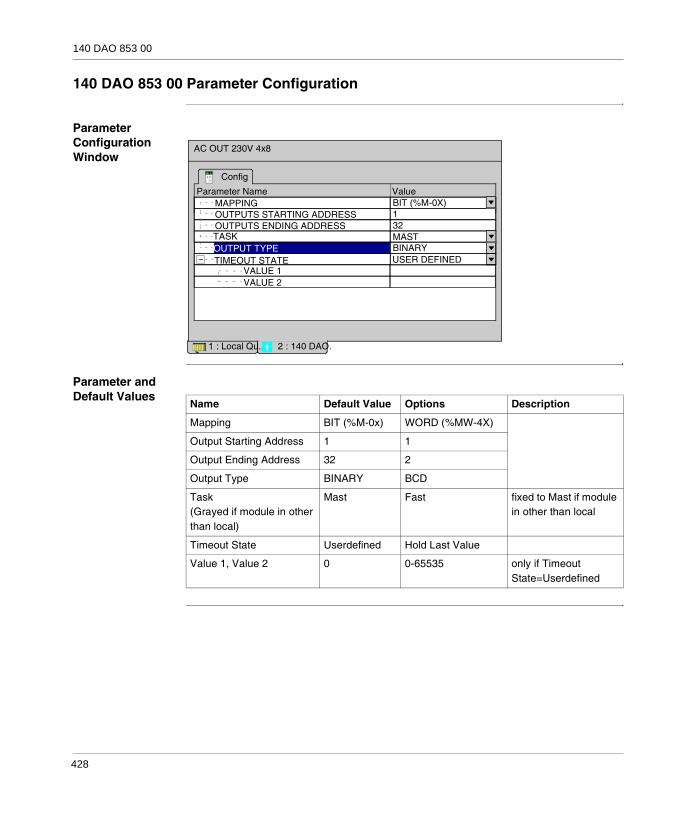
140 DAO 853 00
140 DAO 853 00 Parameter Configuration
Parameter Configuration Window
Parameter and Default Values
AC OUT 230V 4x8
Config
Parameter Name ValueMAPPING BIT (%M-0X)OUTPUTS STARTING ADDRESS 1OUTPUTS ENDING ADDRESS 32
OUTPUT TYPE BINARY
1 : Local Qu... 2 : 140 DAO.
TIMEOUT STATE USER DEFINEDVALUE 1VALUE 2
TASK MAST
Name Default Value Options Description
Mapping BIT (%M-0x) WORD (%MW-4X)
Output Starting Address 1 1
Output Ending Address 32 2
Output Type BINARY BCD
Task(Grayed if module in other than local)
Mast Fast fixed to Mast if module in other than local
Timeout State Userdefined Hold Last Value
Value 1, Value 2 0 0-65535 only if Timeout State=Userdefined
428

43
140 DRA 840 00: Relay 16x1 Normally Open OUT ModuleOverview
Purpose The following chapter provides information of the Quantum 140 DRA 840 00 Module.
What's in this Chapter?
This chapter contains the following topics:
Topic Page
Presentation 430
Indicators 431
Wiring Diagram 432
Specifications 434
140 DRA 840 00 Parameter Configuration 436
429

140 DRA 840 00
Presentation
Function The Relay Output 16x1 Normally Open module is used to switch a voltage source using 16 relays with normally open contacts.
Illustration The following figure shows the 140 DRA 840 00 module and its components.
1 Model Number, Module Description, Color Code
2 LED Display
3 Fuse Cutouts
4 Field Wiring Terminal Strip
5 Removable Door
6 Customer Identification Label (Fold label and place it inside door)
Note: The field wiring terminal strip (Modicon #140 XTS 002 00) must be ordered separately. (The terminal strip includes the removable door and label.)
140DRA 840 00
X X
XXXXXXXXXXXXXXXXXXXX
XXXXXXXXXXXXXXXXXXXXX
23
6
8
10
1214
16
18
20
21
232527
29
31
3335
37
1
4
7
9
11
13
1517
19
22
24
26
28
30
32
34
3638
1
2
3
4 5
6
430

140 DRA 840 00
Indicators
Illustration The following table shows the LED indicators for the 140 DRA 840 00 module.
Descriptions The following table shows the LED descriptions for the 140 DRA 840 00 module.
Active F
91102113
1245678
13141516
123
45678
91011
1213141516
LEDs Color Indication when ON
Active Green Bus communication is present.
F Red A fault (external to the module) has been detected.
1 ... 16 Green The indicated point or channel is turned ON.
431
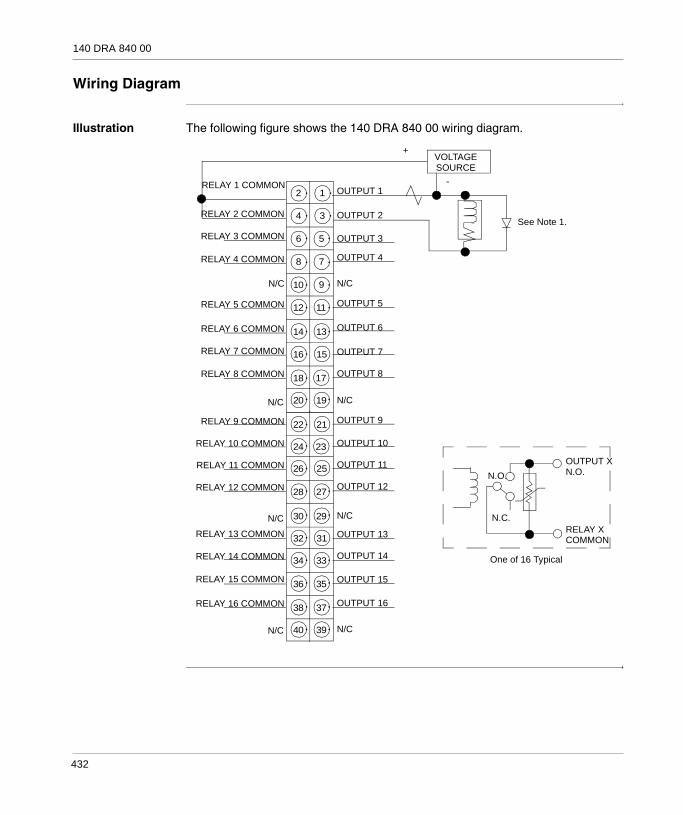
140 DRA 840 00
Wiring Diagram
Illustration The following figure shows the 140 DRA 840 00 wiring diagram.
2
10
4
6
8
12
14
16
18
20
22
24
26
28
30
32
34
36
38
40 39
37
35
33
31
29
27
25
23
21
19
17
15
13
11
9
7
5
3
1 OUTPUT 1
OUTPUT 2
OUTPUT 3
OUTPUT 4
N/C
RELAY 1 COMMON
RELAY 2 COMMON
RELAY 3 COMMON
RELAY 4 COMMON
N/C
RELAY 5 COMMON
RELAY 6 COMMON
RELAY 7 COMMON
RELAY 8 COMMON
N/C
N/C
N/C
N/C
N/C
N/C
OUTPUT 5
OUTPUT 6
OUTPUT 7
OUTPUT 8
RELAY 9 COMMON
RELAY 10 COMMON
RELAY 11 COMMON
RELAY 12 COMMON
RELAY 13 COMMON
RELAY 14 COMMON
RELAY 15 COMMON
RELAY 16 COMMON
OUTPUT 9
OUTPUT 10
OUTPUT 11
OUTPUT 12
OUTPUT 13
OUTPUT 14
OUTPUT 15
OUTPUT 16
VOLTAGESOURCE
+
-
See Note 1.
N.O.
N.C.
OUTPUT XN.O.
RELAY XCOMMON
One of 16 Typical
432

140 DRA 840 00
Notes on Wiring Diagram
For 125 VDC inductive loads, external clamping is recommended to extend relay contact life. (1N 4004 or equivalent).N / C = Not Connected.N.O. = Normally Open.N.C. = Normally Closed.
Note: When field wiring the I/O module, the maximum wire size that should be used is 1-14 AWG or 2-16 AWG; the minimum size is 20 AWG.
433

140 DRA 840 00
Specifications
General Specifications
General Specifications
Operating Voltage
Operating Voltage
Maximum Load Current
Maximum Load Current
Minimum Load Current
Minimum Load Current
Module Type 16 OUT (normaly open)
External Power Not required for this module
Power Dissipation 5.5 W + 0.5 W x input points ON
Bus Current required (Module) 1100 mA
I/O map 1 output word
AC 20 ... 250 VAC
DC 5 ... 30 VDC30 ... 150 VDC (reduced load Current)
Each Point 2 A max. @ 250 VDC @ 60 degrees C ambient, resistive load1 A Tungsten lamp load1 A @ a power factor of 0.41/8 hp @ 125 / 250 VAC
Each Point (30 ... 150 VDC)
300 mA (restive load)100 mA (L/R = 10 msec)
Surge Current (max.) 10 A capacitive load @ t = 10 ms
Minimum Load Current
50 mANote: Minimum load Current if the contact is used at rated loads of 5 ... 150 VDC or 20 ... 250 VDC
Each Point 2 A max. @ 250 VDC @ 60 degrees C ambient, resistive load
OFF State Leakage < 100 μA
434

140 DRA 840 00
Isolation Isolation
Response Response
Relay Relay
Fuses Fuses
Output to Output 1780 VAC rms for one minute
Field to Bus 1780 VAC rms for one minute2500 for one minute
OFF - ON 10 ms (max.)
ON - OFF 20 ms (max.)
Relay type Form A
Contact Protection Varistor 275 V (internal)
Mechanical Operations 10,000,000
Electrical Operations 200,000 (resistive load @ max. Voltage and Current)
Electrical Operations (30 ... 150 VDC) (see note below)
100,000 @ 300 mA (resistive load)50,000 @ 500 mA (resistive load)100,000 @ 100 mA (L/R = 10 msec)100,000 Interposing Relay (Westinghouse Style 606B, Westinghouse type SG, Struthers Dunn 219 x 13 XP)
Switching Capability 500 VA (resistive load)
Internal None
External User discretion
Note: Relay contact life for inductive loads may be significantly increased by using external contact protection such as a clamping diode across the load.
435

140 DRA 840 00
140 DRA 840 00 Parameter Configuration
Parameter Configuration Window
Parameter and Default Values
RELAY OUT 16x1 NO
Config
Parameter Name ValueMAPPING BIT (%M-0X)OUTPUTS STARTING ADDRESS 1OUTPUTS ENDING ADDRESS 16
OUTPUT TYPE BINARY
1 : Local Qu... 2 : 140 DRA.
TIMEOUT STATE USER DEFINEDVALUE
TASK MAST
0
Name Default Value Options Description
Mapping BIT (%M-0x) WORD (%MW-4X)
Outputs Starting Address 1 1
Outputs Ending Address 16 1
Task(Grayed if module in other than local)
MAST FASTAUX0AUX1AUX2AUX3
fixed to MAST if module in other than local
Output Type BINARY BCD
Timeout State USER DEFINED HOLD LAST VALUE
Value 0 0-65535 only if Timeout State=USER DEFINED
436

44
140 DRC 830 00: Relay 8x1 Normally Open / Normally Closed OUT ModuleOverview
Purpose The following chapter provides information of the Quantum 140 DRC 830 00 Module.
What's in this Chapter?
This chapter contains the following topics:
Topic Page
Presentation 438
Indicators 439
Wiring Diagram 440
Specifications 442
140 DRC 830 00 Parameter Configuration 445
437

140 DRC 830 00
Presentation
Function The Relay Output 8x1 Normally Open / Normally Closed module is used to switch voltage sources using eight relays with normally open and normally closed contacts.
Illustration The following figure shows the 140 DRC 830 00 module and its components.
1 Model Number, Module Description, Color Code
2 LED Display
3 Fuse Cutouts
4 Field Wiring Terminal Strip
5 Removable Door
6 Customer Identification Label (Fold label and place it inside door)
Note: The field wiring terminal strip (Modicon #140 XTS 002 00) must be ordered separately. (The terminal strip includes the removable door and label.)
140DRC 830 00
X X
XXXXXXXXXXXXXXXXXXXX
XXXXXXXXXXXXXXXXXXXXX
23
6
8
10
1214
16
18
20
21
232527
29
31
3335
37
1
4
7
9
11
13
1517
19
22
24
26
28
30
32
34
3638
1
2
3
4 5
6
438

140 DRC 830 00
Indicators
Illustration The following table shows the LED indicators for the 140 DRC 830 00 module.
Descriptions The following table shows the LED descriptions for the 140 DRC 830 00 module.
Active F
123
45678
LEDs Color Indication when ON
Active Green Bus communication is present.
F Red A fault (external to the module) has been detected.
1 ... 8 Green The indicated point or channel is turned ON.
439

140 DRC 830 00
Wiring Diagram
Illustration The following figure shows the 140 DRC 830 00 wiring diagram.
2
10
4
6
8
12
14
16
18
20
22
24
26
28
30
32
34
36
38
40 39
37
35
33
31
29
27
25
23
21
19
17
15
13
11
9
7
5
3
1 OUTPUT 1
OUTPUT 1
OUTPUT 2
N/CN/C
RELAY 3 COMMON
N/C
N/C
N/C
N/C
N/C
OUTPUT 3
RELAY 5 COMMON
RELAY 7 COMMON
RELAY 8 COMMON
OUTPUT 5
OUTPUT 6
OUTPUT 7
OUTPUT 8
VOLTAGESOURCE
+
-
See Note 2.
N.O.
RELAY XCOMMON
RELAY 2 COMMON
N/C
N/C
OUTPUT XN.O.
OUTPUT XN.C.
N.C.
One of Eight Typical
N/C
RELAY 4 COMMON
N/C
N/C
N/C
RELAY 6 COMMON
N/C
N/C
RELAY 1 COMMON
N/C
OUTPUT 2
OUTPUT 3
OUTPUT 4
OUTPUT 4
OUTPUT 5
OUTPUT 6
OUTPUT 7
OUTPUT 8
440

140 DRC 830 00
Notes on Wiring Diagram
When switching DC voltages, it is recommended that the source be connected to the common pin and the load be connected to the N.O. or N.C. contact.For 125 VDC inductive loads, external clamping is recommended to extend relay contact life (1N 4004 or equivalent).N / C = Not Connected.N.O. = Normally Open.N.C. - Normally Closed.
Note: When field wiring the I/O module, the maximum wire size that should be used is 1-14 AWG or 2-16 AWG; the minimum size is 20 AWG.
441

140 DRC 830 00
Specifications
General Specifications
General Specifications
Operating Voltage
Operating Voltage
Maximum Load Current
Maximum Load Current
Module Type 8 OUT (normaly open)
External Power Not required for this module
Power Dissipation 2.75 W + 0.5 W x input points ON
Bus Current required (Module) 560 mA
I/O map 0.5 output word
AC 20 ... 250 VAC
DC 5 ... 30 VDC30 ... 150 VDC (reduced load Current)
Each Point 5 A max. @ 250 VDC @ 60 degrees C ambient, resistive load2 A Tungsten lamp load3 A @ a power factor of 0.41/4 hp @ 125 / 250 VAC
Each Point (30 ... 150 VDC)
300 mA (restive load)100 mA (L/R = 10 msec)
Maximum module Current
40 A (see the derating curve below)
Surge Current (max.)
20 A capacitive load @ t = 10 ms
442

140 DRC 830 00
The following figure shows the relay derating curve.
Minimum Load Current
Minimum Load Current
Isolation Isolation
Response Response
Relay Relay
TOTA
L M
OD
ULE
C
UR
REN
T (A
)
Relay Derating Curve
AMBIENT TEMPERATURE (Degrees C)
100
203040
40 50 60
Minimum Load Current 50 mANote: Minimum load Current if the contact is used at rated loads of 5 ... 150 VDC or 20 ... 250 VDC
OFF State Leakage < 100 μA
Output to Output 1780 VAC rms for one minute
Field to Bus 1780 VAC rms for one minute2500 for one minute
OFF - ON 10 ms (max.)
ON - OFF 20 ms (max.)
Relay type Form C, NO / NC contacts
Contact Protection Varistor 275 V (internal)
Mechanical Operations 10,000,000
Electrical Operations 200,000 (resistive load @ max. Voltage and Current)
443

140 DRC 830 00
Fuses Fuses
Electrical Operations (30 ... 150 VDC) (see note below)
100,000 @ 300 mA (resistive load)50,000 @ 500 mA (resistive load)100,000 @ 100 mA (L/R = 10 msec)100,000 Interposing Relay (Westinghouse Style 606B, Westinghouse type SG, Struthers Dunn 219 x 13 XP)
Switching Capability 500 VA (reistive load)
Internal None
External User discretion
Note: Relay contact life for inductive loads may be significantly increased by using external contact protection such as a clamping diode across the load.
444
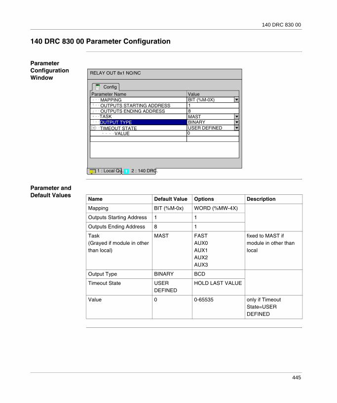
140 DRC 830 00
140 DRC 830 00 Parameter Configuration
Parameter Configuration Window
Parameter and Default Values
RELAY OUT 8x1 NO/NC
Config
Parameter Name ValueMAPPING BIT (%M-0X)OUTPUTS STARTING ADDRESS 1OUTPUTS ENDING ADDRESS 8
OUTPUT TYPE BINARY
1 : Local Qu... 2 : 140 DRC.
TIMEOUT STATE USER DEFINEDVALUE
TASK MAST
0
Name Default Value Options Description
Mapping BIT (%M-0x) WORD (%MW-4X)
Outputs Starting Address 1 1
Outputs Ending Address 8 1
Task(Grayed if module in other than local)
MAST FASTAUX0AUX1AUX2AUX3
fixed to MAST if module in other than local
Output Type BINARY BCD
Timeout State USER DEFINED
HOLD LAST VALUE
Value 0 0-65535 only if Timeout State=USER DEFINED
445

140 DRC 830 00
446

45
140 DVO 853 00: 10 ... 30 VDC 32x1 Verified OUT ModuleOverview
Purpose The following chapter provides information of the Quantum 140 DVO 853 00 Module.
What's in this Chapter?
This chapter contains the following topics:
Topic Page
Presentation 448
Indicators 449
Wiring Diagram 450
Specifications 451
Maintenance 453
Addressing 454
Parameter Configuration 456
447

140 DVO 853 00
Presentation
Function The Quantum 140 DVO 853 00 is a 10 ... 30 VDC, 32 point output module with diagnostic capability. The module will detect and report the output state sensed at the field connector and, depending on the selected configuration, will verify that the output point is in the state commanded by the PLC. The module is configured in four groups of eight outputs.
Illustration The following figure shows the 140 DVO 853 00 module and its components.
1 Model Number, Module Description, Color Code
2 LED Display
3 Fuse Cutouts
4 Field Wiring Terminal Strip
5 Removable Door
6 Customer Identification Label (Fold label and place it inside door)
Note: The field wiring terminal strip (Modicon #140 XTS 002 00) must be ordered separately. (The terminal strip includes the removable door and label.)
140DVO 853 00
X X
XXXXXXXXXXXXXXXXXXXX
XXXXXXXXXXXXXXXXXXXXX
23
6
8
10
1214
16
18
20
21
232527
29
31
3335
37
1
4
7
9
11
13
1517
19
22
24
26
28
30
32
34
3638
1
2
3
4 5
6
448

140 DVO 853 00
Indicators
Illustration The following table shows the LED indicators for the 140 DVO 853 00 module.
Descriptions The following table shows the LED descriptions for the 140 DVO 853 00 module.
Active F
91102113
1245678
13141516
171819
2021222324
252627
2829303132
LEDs Color Indication when ON
Active Green Bus communication is present.
F Red A fault (external to the module) has been detected.
1 ... 32 Green The indicated point or channel is turned ON.
449

140 DVO 853 00
Wiring Diagram
Illustration The following figure shows the 140 DVO 853 00 wiring diagram.
Note: When field wiring the I/O module, the maximum wire size that should be used is 1-14 AWG or 2-16 AWG; the minimum size is 20 AWG.
GROUP C COMMON
GROUP B COMMON
OUTPUT 5
OUTPUT 9
OUTPUT 13
OUTPUT 17
OUTPUT 19
OUTPUT 21
OUTPUT 32
OUTPUT 30
OUTPUT 26
OUTPUT 24
OUTPUT 22
OUTPUT 20
OUTPUT 18
2
10
4
6
8
12
14
16
18
20
22
24
26
28
30
32
34
36
38
40 39
37
35
33
31
29
27
25
23
21
19
17
15
13
11
9
7
5
3
1+-
OUTPUT 25
OUTPUT 27
OUTPUT 29
OUTPUT 31
GROUP D COMMON
OUTPUT 23
OUTPUT 15
OUTPUT 11
GROUP A COMMON
OUTPUT 7
OUTPUT 3
OUTPUT 10.75 A
0.75 A
OUTPUT 4
OUTPUT 6
OUTPUT 2
OUTPUT 8
OUTPUT 10
OUTPUT 12
OUTPUT 16
GROUP A SUPPLY
GROUP B SUPPLY
OUTPUT 28
GROUP D SUPPLY
GROUP C SUPPLY
0.75 A
0.75 A
OUTPUT 14Note:When driving a load fromtwo different points, ablocking diode is requiredfor each point. These di-odes (shown above) willprevent false fault reportingwhen only one of the pointsis commanded ON.
OUTPUT 1
OUTPUT 3
450

140 DVO 853 00
Specifications
General Specifications
General Specifications
Voltage Voltage
Maximum Load Current
Maximum Load Current
Load Inductance / Capacitance (max.)
Load Inductance / Capacitance (max.)
Module Type 32 OUT (4 groups x 8 points)
External Power 10 ... 30 VDC
Power Dissipation 2.5 W + 0.1 W x input points ON + 0.4 V x total load Currents
Bus Current required (Module)
500 mA
I/O map 2 input word2 output word
Fault Detection Blown fuse detect, loss of field power, incorrect output state.
Operating Voltage (max.)
10 ... 30 VDC
Absolute Voltage (max.) 50 VDC for 1.0 ms decaying voltage pulse
ON State Drop / Point 0.4 VDC @ 0.5 A
Each Point 0.5 A
Each Group 4.0 A
Per Module 16 A
OFF State Leakage / Point
0.4 mA @ 30 VDC
Surge Current (max.) Each Point: 2.5 A @ 1 ms duration (no more than 6 per minute)
Load Inductance (max.) 0.5 Henry @ 4 Hz switch frequency, or:
Load Capacitance (max.) 75 mF
Tungsten Load (max.) 2.5 W @ 10 VDC3 W @ 12 VDC6 W @ 24 VDC
L = 0.5
l2 F
where: L = Load inductance (henry) l = Load current (A)
F = Switching Frequency (Hz)
451
140 DVO 853 00
Isolation / Protection
Isolation / Protection
Response Response
Group to Group 500 VAC rms for 1 minute
Group to Bus 1780 VAC rms for 1 minute
Output Protection Transient Voltage Suppression (internal), overload (short circuit) protecton
OFF - ON 1 ms (typical), 2 ms (max.)
ON - OFF 1 ms (typical), 2 ms (max.)
452

140 DVO 853 00
Maintenance
Fuses Fuses
Illustration The following figure shows the 140 DVO 853 00 module Fuse Locations.
Internal 5.0 Amp fuse per group, P/N 0043502405
External Nor required. If desired, q 3/4 A, 250 V fuse(P/N 57-0078-00) may be used
CAUTIONPossible danger to equipment or personnel.Turn off power to the module and remove the field wiring terminal strip to gain access to fuses.Failure to follow this precaution can result in injury or equipment damage.
Points1-8
140DVO 853 00
X
Fuse Locations
Points17-24
Points25-32
Points9-16
453

140 DVO 853 00
Addressing
Flat Addressing This module requires 32 contiguous, output references (%M) or 2 contiguous output words (%MW) for output data and 32 contiguous, input references (%I) or 2 contiguous input words (%IW) for verification input data. For a description of how to access the input points, please refer to Discrete I/O Bit Numbering, p. 36.Output Words:
Input Words:
Topological Addressing
Topological addresses in Bit Mapping format:
1 2 3 4 5 6 7 10 11 12 13 14 15 168 9
17 18 19 20 21 22 23 26 27 28 29 30 31 3224 25
Output Point 1
MSB - Second Word
MSB - First Word
OutputPoint 17
1 2 3 4 5 6 7 10 11 12 13 14 15 168 9
17 18 19 20 21 22 23 26 27 28 29 30 31 3224 25
Input SensePoint 1
MSB - Second Word
MSB - First Word
Input SensePoint 17
Point I/O Object Comment
Input 1 %I[\b.e\]r.m.1 Value
Input 2 %I[\b.e\]r.m.2 Value
• • •
Input 31 %I[\b.e\]r.m.31 Value
Input 32 %I[\b.e\]r.m.32 Value
Output 1 %Q[\b.e\]r.m.1 Value
Output 2 %Q[\b.e\]r.m.2 Value
• • •
Output 31 %Q[\b.e\]r.m.31 Value
Output 32 %Q[\b.e\]r.m.32 Value
454

140 DVO 853 00
Topological addresses in Word Mapping format:
Used abbreviations: b = bus, e = equipment (drop), r = rack, m = module slot.
I/O Map Status Byte
The eight bits in the I/O map status byte are used as follows:
The voltage fault bit is set when the field supply is not present, or the group fuse is blown.The miscompare bit is set when any point within the group does not match its commanded state.
Point I/O Object Comment
Inputword 1 %IW[\b.e\]r.m.1.1 Value
Inputword 2 %IW[\b.e\]r.m.1.2 Value
Outputword 1 %QW[\b.e\]r.m.1.1 Value
Outputword 2 %QW[\b.e\]r.m.1.2 Value
8 7 6 5 4 3 2 1
Group B Voltage FaultGroup C Voltage fault
Group D Voltage Fault
Group A Voltage Fault
Group B MiscompareGroup A Miscompare
Group C MiscompareGroup D Miscompare
455

140 DVO 853 00
Parameter Configuration
Parameter and Default values
Parameter Configuration Window
Verified Output 10-30 V
Config
Parameter Name ValueMAPPING BIT (%I-1x%M-0X)
OUTPUTS STARTING ADDRESS
1
OUTPUTS ENDING ADDRESS 31
AUTOMATIC RESTART NO
1 : Local Qu... 2 : 140 DVO.
GROUP_1STATUS INPUT
TASK MASTOUTPUT SHUTDOWN STATE
INPUTS STARTING ADDRESSINPUTS ENDING ADDRESS
DISABLE
311
FAIL STATESUSER DEFINED
VERIFIEDDISABLED
GROUP_2GROUP_3GROUP_4
456

140 DVO 853 00
Name Default Value Options Description
Mapping BIT (%I-1x%M-0x) WORD (%MW-4X)
Inputs Starting Address 1 1
Inputs Ending Address 31 2
Outputs Starting Address 1 1
Outputs Ending Address 31 2
Task(Grayed if module in other than local)
MAST FASTAUX0AUX1AUX2AUX3
fixed to MAST if module in other than local
Output Shutdown State DISABLE FAILE STATES
Automatic Restart No Yes
Group_1
Status Input VERIFIED HEALTH
VERIFIED FAULTINPUT ONLYACTUAL
Fail States DISABLE LAST VALUEUSER DEFINED
User Defined 0 0-255 only enabled if Fail States=USER DEFINED
Group_2Group_3Group_4
see Group_1
457

140 DVO 853 00
458

VII
Discrete IN / OUT ModulesAt a Glance
Introduction The following part provides information on the Quantum Discrete IN / OUT modules.
What's in this Part?
This part contains the following chapters:
Chapter Chapter Name Page
46 General Information 461
47 140 DDM 390 00: 24 VDC 2x8 Sink IN / 2x4 Source OUT Module 463
48 140 DDM 690 00: 125 VDC High Power IN/OUT Module 475
49 140 DAM 590 00: 115 VAC 2x8 IN / 2x4 OUT Module 487
459

Discrete IN / OUT Modules
460

46
General InformationDiscrete I/O Logic Circuits
Discrete I/O True High Figure
The following figure shows true high/current sink input/current source output schematic.
Discrete I/O True Low Figure
The following figure shows true low/current source input/current sink output schematic.
Power Supply
+
Load
Output
Current
LOGIC
Input
Current
Common
Power Supply
+
+
Power Supply
Load
Output
Current
LOGIC
Input
Current
Power Supply
+
Common
461

General Information
Current Sinking This describes a physical implementation of the I/O hardware, which when in the true state, sinks current from the external load.
Current Sourcing This describes a physical implementation of the I/O hardware, which when in the true state, sources current to the external load.
462

47
140 DDM 390 00: 24 VDC 2x8 Sink IN / 2x4 Source OUT ModuleOverview
Purpose The following chapter provides information of the Quantum 140 DDM 390 00 Module.
What's in this Chapter?
This chapter contains the following topics:
Topic Page
Presentation 464
Indicators 465
RIO Drop Location 466
Wiring Diagram 467
Specifications 469
Maintenance 471
140 DDM 390 00 Parameter Configuration 472
463
140 DDM 390 00
Presentation
Function The DC Input 24 VDC 2x8 Sink / DC Output 24 VDC 2x4 Source module accepts and switches 24 VDC inputs/outputs and is for use with sink input and source output devices.
Illustration This section contains a photograph of the front panel of the 140 DDM 390 00 moduleThe following figure shows the I/O module and its components.
1 Model Number, Module Description, Color Code
2 LED Display
3 Fuse Cutouts
4 Field Wiring Terminal Strip
5 Removable Door
6 Customer Identification Label (Fold label and place it inside door)
Note: The field wiring terminal strip (Modicon #140 XTS 002 00) must be ordered separately. (The terminal strip includes the removable door and label.)
140DDM 390 00
X X
XXXXXXXXXXXXXXXXXXXX
XXXXXXXXXXXXXXXXXXXXX
23
6
8
10
1214
16
18
20
21
232527
29
31
3335
37
1
4
7
9
11
13
1517
19
22
24
26
28
30
32
34
3638
1
2
3
4 5
6
464
140 DDM 390 00
Indicators
Version Label Figure
The following figure shows the location of the version label.
Illustration The following table shows the LED indicators for the 140 DDM 390 00 module.
Descriptions The following table shows the LED descriptions for the 140 DDM 390 module.
140DDM 390 00DC IN/OUT
DC IN/OUT 24V 16/8 SINK/SOURCEPV: 00 RL: 77 SV: _ _
Active F
123
45678
123
45678
91011
1213141516
LEDs Color Indication when ON
Active Green Bus communication is present.
F Red A fault (external to the module) has been detected.
1 ... 8 (left columns) Green The indicated output point and channel is turned ON.
1 ... 16 (right two columns)
Green The indicated input point and channel is turned ON.
465
140 DDM 390 00
RIO Drop Location
RIO Drop Location Figure
The following figure shows the RIO drop location.
Note: If the 140 DDM 390 00 module is used in a RIO drop, the 140 CRA 93X 00 RIO Drop must be Version 1.04 at a minimum. Check the version label (see below) on the top front of the 140 CRA 93X 00 module and ensure that it is at the proper revision level
140CRA 932 00
RIO DROP S90801.04
466

140 DDM 390 00
Wiring Diagram
Illustration The following figure shows the 140 DDM 390 00 wiring diagram.
2
10
4
6
8
12
14
16
18
20
22
24
26
28
30
32
34
36
38
40 39
37
35
33
31
29
27
25
23
21
19
17
15
13
11
9
7
5
3
1 LN
+ -
INPUT GROUP A COMMON
INPUT 9
INPUT 11
INPUT 13
INPUT15
INPUT GROUP B COMMON
INPUT 7
INPUT 5
INPUT 3
INPUT 1
OUTPUT GROUP B COMMON
OUTPUT 8
OUTPUT 7
OUTPUT 6
OUTPUT 5
OUTPUT GROUP A COMMON
OUTPUT 4
OUTPUT 3
OUTPUT 2
OUTPUT 1
1.25 A
1.25 A
INPUT 2
N/C
N/C
N/C
N/C
N/C
N/C
N/C
N/C
OUTPUT GROUP A SUPPLY
OUTPUT GROUP B SUPPLY
INPUT 4
INPUT 6
INPUT 8
N/C
INPUT 10
INPUT 12
INPUT 14
INPUT 16
N/C
467
140 DDM 390 00
Note: N / C = Not Connected
Note: When field wiring the I/O modules, the maximum wire size that should be used is 1-14 AWG or 2-16 AWG; the minimum size is 20 AWG.
CAUTIONPossible Equipment FailureEach group is protected with a 5 A fuse to protect the module from catastrophic failure. The group fuse will not be guaranteed to protect each output switch for all possible overload conditions. It is recommended that each point be fused with a 1.25 A fuse, Part # 043508930 (Littlefuse 3121.25, 1.25 A, 250 V).Failure to follow this precaution can result in injury or equipment damage.
CAUTIONElectrical safety hazard Turn off power to the module and remove the field wiring terminal strip to gain access to fuses.Failure to follow this precaution can result in injury or equipment damage.
468

140 DDM 390 00
Specifications
General Specifications
General Specifications
Input Rating Input Rating
Absolute Maximum Input
Absolute Maximum Input
Voltage (Output) Voltage (Output)
Module Type 16 IN (2 groups x 8 points)8 OUT (2 groups x 4 points)
External Power Not required for this module
Power Dissipation 1.75 W + 0.36 x input points ON + 1.1 V x total outputs load Currents
Bus Current required (Module) 330 mA
I/O map 1 input word0.5 output word
Fault Detection Input: NoneOutput: Blown fuse detect, loss of field power.
ON level voltage +15 ... +30 VDC
ON level current 2.0 mA (min.)
OFF leve voltage +3 ... +5 VDC
OFF level current 0.5 mA (max.)
Internal Resistance 2.5 kohm
Continuous 30 VAC
1.3 ms 56 VAC decaying pulse
Operating Voltage (max.) 19.2 ... 30 VDC
Absolute Voltage (max.) 56 VDC for 1.3 ms decaying voltage pulse
ON State Drop / Point 0.4 VDC @ 0.5 A
469

140 DDM 390 00
Maximum Load Current
Maximum Load Current
Load Inductance / Capacitance (max.)
Load Inductance / Capacitance (max.)
Isolation Isolation
Response (Input and Output)
Response (Input and Output)
Module Protection
Module Protection
Each Point 0.5 A
Each Group 2.0 A
Per Module 4 A
OFF State Leakage / Point 0.4 mA @ 30 VDC
Surge Current (max.) Each Point: 5 A @ 500 ms duration (no more than 6 per minute)
Load Inductance (max.)
0.5 Henry @ 4 Hz switch frequency, or:
Load Capacitance (max.)
50 microF
L = 0.5
l2 F
where: L = Load inductance (henry) l = Load current (A)
F = Switching Frequency (Hz)
Group to Group 500 VAC rms for 1 minute
Group to Bus 1780 VAC rms for 1 minute
OFF - ON 1 ms (max) - (resistive load output)
ON - OFF 1 ms (max) - (resistive load output)
Input Protection Resistor limited
Output Protection Transient Voltage Suppression (internal)
470

140 DDM 390 00
Maintenance
Fuses Fuses
Illustration The following figure shows the fuse locations of the 140 DDM 390 00 module.
Input Internal - None External - User discretion
Output Internal - 5 A fuse for each group (Part # 043502405 or equivalent). Forthe location of the fuses, see figureExternal - 5 A for each group
CAUTION
Possible injury to personnel or equipment.
Turn off power to the module and remove the field wiring terminal strip to gain access to fuses.
Failure to follow this precaution can result in injury or equipment damage.
140DDM 390 00
X
Fuse LocationsPoints
1-4
Points5-8
471

140 DDM 390 00
140 DDM 390 00 Parameter Configuration
Parameter Configuration Window
DC IN/OUT 24V 16x8
Config
Parameter Name ValueMAPPING BIT (%I-1x%M-0X)
OUTPUTS STARTING ADDRESS
1
OUTPUTS ENDING ADDRESS 8
OUTPUT TYPE BINARY
1 : Local Qu... 2 : 140 DDM.
TIMEOUT STATE USER DEFINEDVALUE
TASK MASTINPUT TYPE
INPUTS STARTING ADDRESSINPUTS ENDING ADDRESS
BINARY
161
0
472

140 DDM 390 00
Parameter and Default Values
Name Default Value Options Description
Mapping BIT (%I-1x%M-0x)
WORD (%IW-3x%MW-4X)
Inputs Starting Address 1 1
Inputs Ending Address 16 1
Outputs Starting Address
1 1
Outputs Ending Address 8 1
Task(Grayed if module in other than local)
MAST FASTAUX0AUX1AUX2AUX3
fixed to MAST if module in other than local
Input Type BINARY BCD
Output Type BINARY BCD
Timeout State USER DEFINED HOLD LAST VALUE
Value 0 0-65535 only enabled if Timeout State=USER DEFINED
473

140 DDM 390 00
474

48
140 DDM 690 00: 125 VDC High Power IN/OUT ModuleOverview
Purpose The following chapter provides information of the Quantum 140 DDM 690 00 Module.
What's in this Chapter?
This chapter contains the following topics:
Topic Page
Presentation 476
Indicators 478
Wiring Diagram 480
Specifications 482
140 DDM 690 00 Parameter Configuration 485
475

140 DDM 690 00
Presentation
Function The 125 VDC High Power IN/OUT module provides four isolated outputs and four grouped inputs. The outputs switch 24 to 125 VDC powered loads and are for use with sink and source devices. The outputs also have short-circuit sense, indication, and shutdown circuitry. The inputs accept 125 VDC inputs and are for use with source output devices. The inputs have software-selectable response times to provide additional input filtering.
Illustration This section contains a photograph of the front panel of the 140 DDM 690 00 moduleThe following figure shows the I/O module and its components.
1 Model Number, Module Description, Color Code
2 LED Display
3 Fuse Cutouts
4 Field Wiring Terminal Strip
5 Removable Door
6 Customer Identification Label (Fold label and place it inside door)
Note: The field wiring terminal strip (Modicon #140 XTS 002 00) must be ordered separately. (The terminal strip includes the removable door and label.)
140DDM 690 00
X X
XXXXXXXXXXXXXXXXXXXX
XXXXXXXXXXXXXXXXXXXXX
23
6
8
10
1214
16
18
20
21
232527
29
31
3335
37
1
4
7
9
11
13
1517
19
22
24
26
28
30
32
34
3638
1
2
3
4 5
6
476

140 DDM 690 00
Note: The following information baselines minimum version levels that will support this module.
477

140 DDM 690 00
Indicators
Version Levels Table
The following table shows the version levels for the Module Types.
Version Label Figure
The following figure shows the version number location.
Products Minimum Version Level (see label illustration below)
User Action Required
CPUs and NOMs
< V02.20 Executive upgrade to ≥ V02.10
≥ V02.20 None
RIOs < V02.00 Module upgrade
≥ V02.00 and < V02.20 Executive upgrade to ≥ V01.10
≥ V02.20 None
DIOs < V02.10 Module upgrade
≥ V02.10 None
Note: The version label, see figure, is found on the top front of the module.
140DDM 690 00125 VDC 4I/4O
125VDC 4I/4O HPOSINK/SOURCEPV: 00 RL: 77 SV:__
478
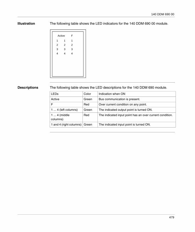
140 DDM 690 00
Illustration The following table shows the LED indicators for the 140 DDM 690 00 module.
Descriptions The following table shows the LED descriptions for the 140 DDM 690 module.
Active F
1 112 223 334 44
LEDs Color Indication when ON
Active Green Bus communication is present.
F Red Over current condition on any point.
1 ... 4 (left columns) Green The indicated output point is turned ON.
1 ... 4 (middle columns)
Red The indicated input point has an over current condition.
1 and 4 (right columns) Green The indicated input point is turned ON.
479

140 DDM 690 00
Wiring Diagram
Illustration The following figure shows the 140 DDM 690 00 wiring diagram.
OUTPUT 1 (+) OUTPUT 1 (-)+-
2
10
4
6
8
12
14
16
18
20
22
24
26
28
30
32
34
36
38
40 39
37
35
33
31
29
27
25
23
21
19
17
15
13
11
9
7
5
3
1
+-
-+
OUTPUT 1 (-)
N/C
N/C
N/C
OUTPUT 2 (-)
OUTPUT 3 (-)
OUTPUT 3 (-)
OUTPUT 2 (-)
N/C
N/C
N/C
OUTPUT 4 (-)
OUTPUT 4 (-)
N/C
125 VDC INPUT 1
125 VDC INPUT 3
N/C
N/C
INPUT GROUP B COMMON
N/C
N/C
N/C
125 VDC INPUT 4
125 VDC INPUT 2
N/C
OUTPUT 4 (+)
OUTPUT 4 (+)
N/C
N/C
OUTPUT 3 (+)
OUTPUT 3 (+)
OUTPUT 2 (+)
OUTPUT 2 (+)
N/C
N/C
N/C
OUTPUT 1 (+) OUTPUT Sourcing
OUTPUT Sinking
480

140 DDM 690 00
CAUTIONPolarity awarenessThe output points are not protected against reverse polarity. Reverse polarity will turn an output point ON.Failure to follow this precaution can result in injury or equipment damage.
Note: Each output has two terminals for multiple wire connections.N / C = Not Connected.
Note: When field wiring the I/O modules, the maximum wire size that should be used is 1-14 AWG or 2-16 AWG; the minimum size is 20 AWG.
481

140 DDM 690 00
Specifications
General Specifications
General Specifications
Input Rating Input Rating
Input Response (OFF-ON, ON-OFF)
Input Response (OFF-ON, ON-OFF)
Voltage (Output) Voltage (Output)
Module Type 4 IN (4 groups x 1 point)4 OUT isolated
External Power Not required for this module
Power Dissipation 0.4 W x (1.0) x number of input points ON + (0.75) x total module outputs Currents
Bus Current required (Module) 350 mA
I/O map 1 input word1 output word
Fault Detection Input: NoneOver Current - each point
ON level voltage +88 ... +156 VDC including ripple
ON level current 2.0 mA (min.)
OFF leve voltage 0 ... +36 VDC
OFF level current 1.2 mA (max.)
Internal Resistance 24 kohms (nominal)
Absolute Voltage (max.) Continuous: 156.2 VDC including ripple
Default Filter 0.5 ms
Non-Default Filter 1.5 ms
Operating Voltage (max.) 19.2 ... 156.2 VDC including ripple
ON State Drop / Point 0.75 VDC @ 4 A
482

140 DDM 690 00
Maximum Load Current
Maximum Load Current
The following figure shows the 140 DDM 690 00 Derating Curve.
Load Inductance / Capacitance (max.)
Load Inductance / Capacitance (max.)
Isolation Isolation
Each Point 4 A continuous
Per Module 16 A continuous (see the derating curve)
OFF State Leakage / Point 1.2 mA @ 150 VDC
Surge Current (max.) Each Point: 30 A @ 500 ms duration
Output Response (OFF-ON, ON-OFF) 0.2 ms (max.) (resistive load output
30Ambient Temperature (_C)
Tota
l Mod
ule
Cur
rent
T
40 50 60
16 A
8 A
Load Inductance (max.)
For switching intervals ≥ 15 secondsper ANSI/IEEE C37.90- 1978/1989):
For repetitive switching:
where: L = Load Inductance (Henry). I = Load Current (A). F = Switching Frequency (Hz)
Load Capacitance (max.)
0.1 microF @ 150 VDC0.6 microF @ 24 VDC
L ≤9
I2
L ≤9
I F2
Input Group to Output 1780 VAC rms for 1 minute
Output to Output 2500 VAC rms for 1 minute
483

140 DDM 690 00
Module Protection
Module Protection
Fuses Fuses
Input Protection Resistor limited
Output Protection Transient Voltage Suppresion (internal)
Input Internal - NoneExternal - User discretion
Output Each output is protected by an electronic shutdown:For current output surges between 4 A and 30 A, the input point will shutdown after 0.5 s. For current surges greater than 30 A, the output will shutdown immediately.
484

140 DDM 690 00
140 DDM 690 00 Parameter Configuration
Parameter Configuration Window
Parameter and Default Values
125VDC 4I/ 4O HPO
Config
Parameter Name ValueMAPPING BIT (%I-1x%M-0X)
OUTPUTS STARTING ADDRESS
1
OUTPUTS ENDING ADDRESS 8
FILTER SELECTION 0.5 ms
1 : Local Qu... 2 : 140 DDM.
TIMEOUT STATE USER DEFINEDVALUE
TASK MASTDUAL MODE
INPUTS STARTING ADDRESSINPUTS ENDING ADDRESS
DISABLE
81
0
Name Default Value Options Description
Mapping BIT (%I-1x%M-0x) WORD (%IW-3x%MW-4X)
Inputs Starting Address 1 1
Inputs Ending Address 8 1
Outputs Starting Address
1 1
Outputs Ending Address
8 1
Task(Grayed if module in other than local)
MAST FASTAUX0AUX1AUX2AUX3
fixed to MAST if module in other than local
Dual Mode DISABLE ENABLE
Filter Selection 0.5 ms 1.5 ms
Timeout State USER DEFINED HOLD LAST VALUE
Value 0 0-65535 only enabled if Timeout State=USER DEFINED
485

140 DDM 690 00
486

49
140 DAM 590 00: 115 VAC 2x8 IN / 2x4 OUT ModuleOverview
Purpose The following chapter provides information of the Quantum 140 DAM 590 00 Module.
What's in this Chapter?
This chapter contains the following topics:
Topic Page
Presentation 488
Indicators 489
RIO Drop Location 490
Wiring Diagram 491
Specifications 493
Maintenance 496
140 DAM 590 00 Parameter Configuration 497
487

140 DAM 590 00
Presentation
Function The AC Input 115 VAC 2x8 / AC Output 115 VAC 2x4 module accepts 115 VAC inputs and switches 115 VAC loads.
Illustration This section contains a photograph of the front panel of the 140 DAM 590 00 moduleThe following figure shows the 140 DAM 590 00 module and its components.
1 Model Number, Module Description, Color Code
2 LED Display
3 Fuse Cutouts
4 Field Wiring Terminal Strip
5 Removable Door
6 Customer Identification Label (Fold label and place it inside door)
Note: The field wiring terminal strip (Modicon #140 XTS 002 00) must be ordered separately. (The terminal strip includes the removable door and label.)
140DAM 590 00
X X
XXXXXXXXXXXXXXXXXXXX
XXXXXXXXXXXXXXXXXXXXX
23
6
8
10
1214
16
18
20
21
232527
29
31
3335
37
1
4
7
9
11
13
1517
19
22
24
26
28
30
32
34
3638
1
2
3
4 5
6
488

140 DAM 590 00
Indicators
Illustration The following table shows the LED indicators for the 140 DAM 590 00 module.
Descriptions The following table shows the LED descriptions for the 140 DAM 590 module.
Active F
123
45678
123
45678
91011
1213141516
LEDs Color Indication when ON
Active Green Bus communication is present.
F Red A fault (external to the module) has been detected.
1 ... 8 (left columns) Green The indicated output point and channel is turned ON.
1 ... 16 (right two columns)
Green The indicated input point and channel is turned ON.
489

140 DAM 590 00
RIO Drop Location
RIO Drop Location Figure
The following figure shows the RIO drop location.
Note: If the 140 DAM 590 00 module is used in a RIO drop, the 140 CRA 93X 00 RIO Drop must be Version 1.04 at a minimum. Check the version label (see below) on the top front of the 140 CRA 93X 00 module and ensure that it is at the proper revision level
140CRA 932 00
RIO DROP S90801.04
490
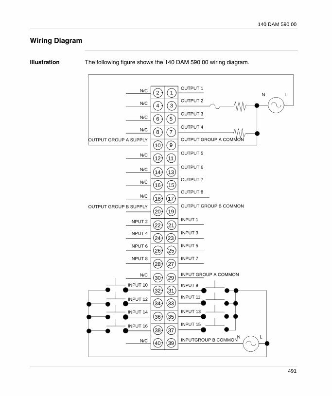
140 DAM 590 00
Wiring Diagram
Illustration The following figure shows the 140 DAM 590 00 wiring diagram.
OUTPUT 1
N
OUTPUT 2
OUTPUT 3
OUTPUT 4
OUTPUT GROUP B COMMON
INPUTGROUP B COMMON
OUTPUT 8
INPUT 1
INPUT 3
INPUT 5
INPUT 7
INPUT 9
INPUT 11
INPUT 13
INPUT 15
N/C
N/C
N/C
N/C
N/C
N/C
N/C
N/C
INPUT 2
N/C
N/C
OUTPUT GROUP A SUPPLY
OUTPUT GROUP B SUPPLY
INPUT 4
INPUT 6
INPUT 8
INPUT 10
INPUT 12
INPUT 14
INPUT 16
INPUT GROUP A COMMON
OUTPUT 7
OUTPUT 6
OUTPUT 5
2
10
4
6
8
12
14
16
18
20
22
24
26
28
30
32
34
36
38
40 39
37
35
33
31
29
27
25
23
21
19
17
15
13
11
9
7
5
3
1
L
OUTPUT GROUP A COMMON
N L
491

140 DAM 590 00
Note: When field wiring the I/O modules, the maximum wire size that should be used is 1-14 AWG or 2-16 AWG; the minimum size is 20 AWG.
CAUTIONElectrical shock hazardTurn off power to the module and remove the field wiring terminal strip to gain access to the fuses.Failure to follow this precaution can result in injury or equipment damage.
CAUTIONWiring CompatibilityIf an external switch is wired to control an inductive load in parallel with the module output, then an external varistor (Harris V390ZA05 or equivalent) must be wired in parallel with the switch.Failure to follow this precaution can result in injury or equipment damage.
492

140 DAM 590 00
Specifications
General Specifications
General Specifications
Operating Voltage and Input Current*
Operating Voltage and Input Current*
Typical Input Impedance
Typical Input Impedance
Absolute Maximum Input
Absolute Maximum Input
Module Type 16 IN (2 groups x 8 points)8 OUT (2 groups x 4 points)
External Power 85 ... 132 VAC required for output groups
Power Dissipation 5.5 W + 1.1 V x Total module load current
Bus Current required 250 mA
I/O map 1 input word0.5 output word
Fault Detection Input: NoneOutput: Blown fuse detect, loss of field power.
50 Hz ON: 85 ... 132 VAC (11.1 mA max)OFF: 0 ... 20 VAC
60 Hz ON: 79 ... 132 VAC (13.2 mA max) OFF: 0 ... 20 VAC* Do not use outside the 47 ... 63 Hz range
Maximum Allowable Leakage Current from an External Device to be recognized as an OFF Condition.
2.1 mA
50 Hz 14.4 kohms capacitive
60 Hz 12 kohms capacitive
Continuous 132 VAC
10 s 156 VAC
1 Cycle 200 VAC
493
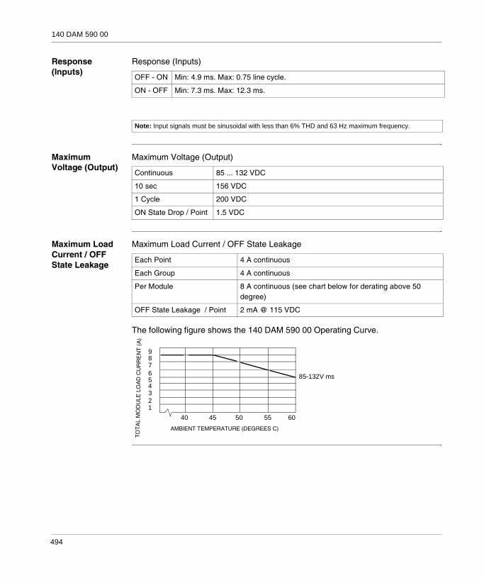
140 DAM 590 00
Response (Inputs)
Response (Inputs)
Maximum Voltage (Output)
Maximum Voltage (Output)
Maximum Load Current / OFF State Leakage
Maximum Load Current / OFF State Leakage
The following figure shows the 140 DAM 590 00 Operating Curve.
OFF - ON Min: 4.9 ms. Max: 0.75 line cycle.
ON - OFF Min: 7.3 ms. Max: 12.3 ms.
Note: Input signals must be sinusoidal with less than 6% THD and 63 Hz maximum frequency.
Continuous 85 ... 132 VDC
10 sec 156 VDC
1 Cycle 200 VDC
ON State Drop / Point 1.5 VDC
Each Point 4 A continuous
Each Group 4 A continuous
Per Module 8 A continuous (see chart below for derating above 50 degree)
OFF State Leakage / Point 2 mA @ 115 VDC
987654321
40 45 50 55 60
85-132V ms
TO
TA
L M
OD
ULE
LO
AD
CU
RR
EN
T (
A)
AMBIENT TEMPERATURE (DEGREES C)
494
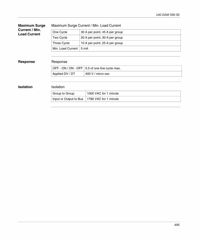
140 DAM 590 00
Maximum Surge Current / Min. Load Current
Maximum Surge Current / Min. Load Current
Response Response
Isolation Isolation
One Cycle 30 A per point, 45 A per group
Two Cycle 20 A per point, 30 A per group
Three Cycle 10 A per point, 25 A per group
Min. Load Current 5 mA
OFF - ON / ON - OFF 0.5 of one line cycle max.
Applied DV / DT 400 V / micro sec
Group to Group 1000 VAC for 1 minute
Input or Output to Bus 1780 VAC for 1 minute
495

140 DAM 590 00
Maintenance
Fuses Fuses
The following figure shows the fuse locations for the 140 DAM 590 00 module.
Input Internal - None External - User discretion
Output Internal - 5 A fuse for each group (Part # 043502405 or equivalent). For the location of the fuses, see figure.External - User discretion
Note: Turn off power to the module and remove the field wiring terminal strip to gain access to the fuses.
140DDO 843 00
X
Fuse LocationsPoints
1-4
Points5-8
496
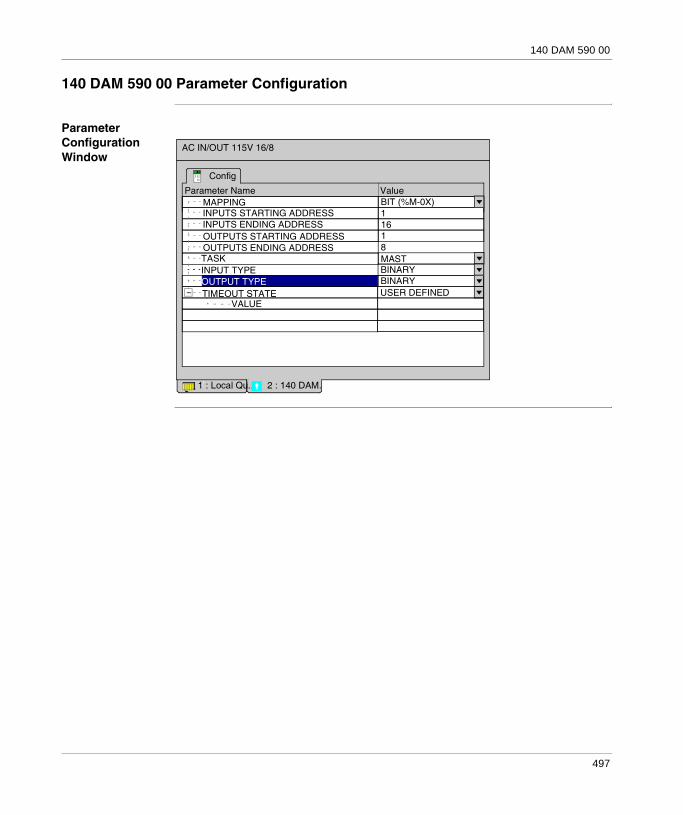
140 DAM 590 00
140 DAM 590 00 Parameter Configuration
Parameter Configuration Window
AC IN/OUT 115V 16/8
Config
Parameter Name ValueMAPPING BIT (%M-0X)
OUTPUTS STARTING ADDRESS
1
OUTPUTS ENDING ADDRESS 8
OUTPUT TYPE BINARY
1 : Local Qu... 2 : 140 DAM.
TIMEOUT STATE USER DEFINEDVALUE
TASK MASTINPUT TYPE
INPUTS STARTING ADDRESSINPUTS ENDING ADDRESS
BINARY
161
497

140 DAM 590 00
Parameter and Default Values
Name Default Value Options Description
Mapping BIT (%I-1x%M-0x)
WORD (%IW-3x%MW-4X)
Inputs Starting Address 1 1
Inputs Ending Address 16 1
Outputs Starting Address
1 1
Outputs Ending Address 8 1
Task(Grayed if module in other than local)
MAST FASTAUX0AUX1AUX2AUX3
fixed to MAST if module in other than local
Input Type BINARY BCD
Output Type BINARY BCD
Timeout State USER DEFINED HOLD LAST VALUE
Value 0 0-65535 only enabled if Timeout State=USER DEFINED
498

VIII
Quantum Intrinsically Safe Analog/Digital ModulesAt a Glance
Introduction The following part provides information on the Quantum Intrinsically Safe Analog/Digital Modules.
What's in this Part?
This part contains the following chapters:
Chapter Chapter Name Page
50 General Information 501
51 140 AII 330 00: Safe Analog IN Module 505
52 140 AII 330 10: Safe Analog IN Module 527
53 140 AIO 330 00: Safe Analog OUT Module 541
54 140 DII 330 00: Safe Discrete IN Module 555
55 140 DIO 330 00: Safe Discrete OUT Module 565
499

Intrinsically Safe Modules
500

50
General InformationOverview
Purpose This chapter provides general information on Intrinsically Safe Modules.
What's in this Chapter?
This chapter contains the following topics:
Topic Page
Purpose and Considerations 502
Wiring Practices 503
501

General Information
Purpose and Considerations
Purpose Intrinsic safety is a technique for ensuring that electrical energy supplied to circuits in a hazardous area is too low to ignite volatile gases either by spark or thermal means. Intrinsically safe circuits use energy limiting devices known as intrinsically safe barriers to prevent excess electrical energy from being applied to electrical equipment located in the hazardous area.
Module Location The Quantum Intrinsically Safe family of modules are entity certified to be installed in safe areas to monitor/control intrinsically safe apparatus located In hazardous areas.
Intrinsically Safe Barriers
All Quantum Intrinsically Safe modules use galvanic isolation to provide the intrinsically safe barrier between them and the field devices located in hazardous areas. Galvanic isolation in the form of an opto-isolatior and DC/DC converter is provided between the field side output circuitry and the Quantum bus circuitry. The maximum agency specified intrinsically safe parameters are:
Intrinsically Safe Power Supply
DC/DC converters in Quantum Intrinsically Safe modules provide intrinsically safe power to field devices located in hazardous areas. No external field power is required where these modules are installed.
Installation of Quantum Intrinsically Safe Modules
Quantum Intrinsically Safe modules are designed to fit into a standard 140 XBP OXX 00 Quantum backplane. The modules can be installed in any slot position in the backplane. (The first slot is normally reserved for the power supply module.)
Hot Swapping
Voc ≤ 28 VDC and Isc ≤ 100mA
WARNINGHot SwapDo not attempt to hot swap a Quantum Intrinsically Safe module.Failure to follow this precaution can result in death, serious injury, or equipment damage.
502
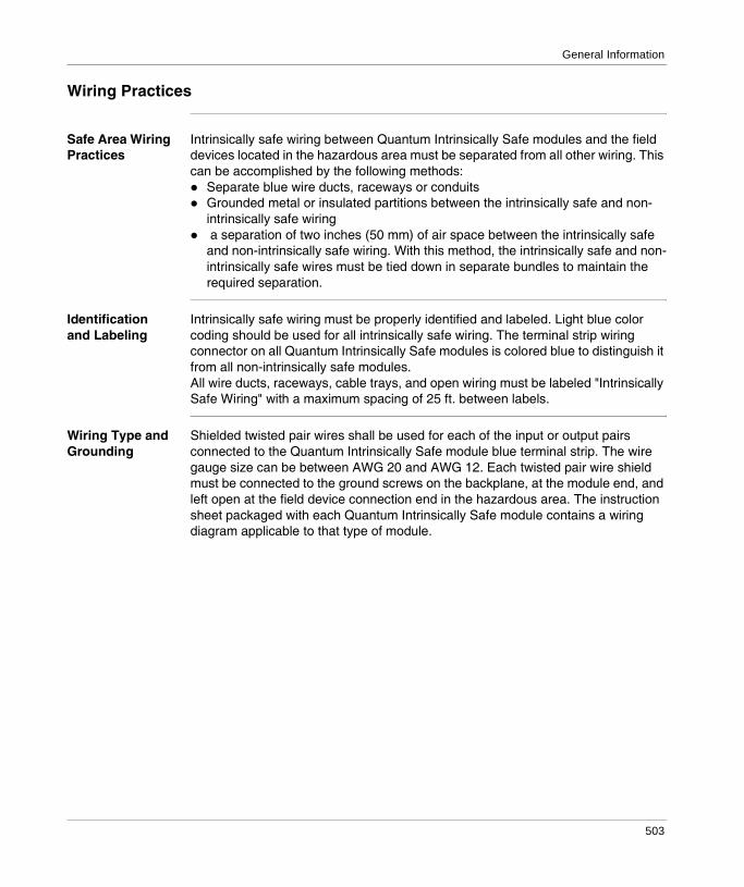
General Information
Wiring Practices
Safe Area Wiring Practices
Intrinsically safe wiring between Quantum Intrinsically Safe modules and the field devices located in the hazardous area must be separated from all other wiring. This can be accomplished by the following methods:
Separate blue wire ducts, raceways or conduitsGrounded metal or insulated partitions between the intrinsically safe and non- intrinsically safe wiring a separation of two inches (50 mm) of air space between the intrinsically safe and non-intrinsically safe wiring. With this method, the intrinsically safe and non-intrinsically safe wires must be tied down in separate bundles to maintain the required separation.
Identification and Labeling
Intrinsically safe wiring must be properly identified and labeled. Light blue color coding should be used for all intrinsically safe wiring. The terminal strip wiring connector on all Quantum Intrinsically Safe modules is colored blue to distinguish it from all non-intrinsically safe modules.All wire ducts, raceways, cable trays, and open wiring must be labeled "Intrinsically Safe Wiring" with a maximum spacing of 25 ft. between labels.
Wiring Type and Grounding
Shielded twisted pair wires shall be used for each of the input or output pairs connected to the Quantum Intrinsically Safe module blue terminal strip. The wire gauge size can be between AWG 20 and AWG 12. Each twisted pair wire shield must be connected to the ground screws on the backplane, at the module end, and left open at the field device connection end in the hazardous area. The instruction sheet packaged with each Quantum Intrinsically Safe module contains a wiring diagram applicable to that type of module.
503

General Information
Intrinsically Safe Wiring Diagram
The following diagram illustrates a Quantum Intrinsically Safe module using a separate raceway to isolate its external wiring to the hazardous area. This is just one of the possible ways of field wiring the module. Other methods would include bundling and laying the intrinsically safe wires in the same wiring trough with the bundled non-intrinsically safe wires, with each bundle tied down and separated by minimum of two inches of air space through out the wiring runs.
Questions Regarding Intrinsically Safe Wiring Practices
The information concerning intrinsic safety wiring practices, is general in-nature and is not intended to cover installation requirements for any specific site. Questions regarding intrinsic safety wiring requirements for your site should be referred to the approval agencies listed
PS CPU
STD I/O M O D U L E
STD I/O M O D U L E
I.S. M O D U L E
STD I/O M O D U L E
BACKPLANE
STANDARD I/OWIRING
INTRINSICALLYSAFE WIRINGLABELS
SAFE WIRING SAFE WIRING
HAZARDOUS
AREA
SAFE
AREA INTRINSICALLY
SAFE WIRINGIN SEPARATE BLUE RACEWAY
(Intrinsically Safe)
504

51
140 AII 330 00: Safe Analog IN ModuleOverview
Purpose The following chapter provides information of the Quantum 140 AII 330 00 Module.
What's in this Chapter?
This chapter contains the following topics:
Topic Page
Presentation 506
Indicators 507
Wiring Diagrams 508
Specifications 517
Addressing 520
Parameter Configuration 523
505

140 AII 330 00
Presentation
Function The Quantum 140 AII 330 00 Intrinsically Safe Analog Input module will interface with eight intrinsically safe analog inputs, which are software-configurable on a module basis with either RTD/Resistance or thermocouple/millivolt inputs.
When it is configured as an RTD/Resistance Input module, it supports 100W, 200W, 500W, and 1000W platinum (American or European) and nickel sensors. The module also allows any mix and match of sensor type or resistance inputs that can be configured by the software.
When it is configured as a Thermocouple/Millivolt Input module, it accepts B, J, K, E, R, S and T type thermocouples. The module also allows any mix and match of thermocouple or millivolt inputs that can be configured by the software.
Illustration The following figure shows the 140 AII 330 00 Intrinsically Safe module and its components.
1 Model Number, Module Description, Color Code2 LED Display3 Fuse Cutouts4 Field Wiring Terminal Strip5 Removable Door6 Customer Identification Label (Fold label and place it inside door)
140AII 330 00
X X
XXXXXXXXXXXXXXXXXXXX
XXXXXXXXXXXXXXXXXXXXX
23
6
8
10
1214
16
18
20
21
232527
29
31
3335
37
1
4
7
9
11
13
1517
19
22
24
26
28
30
32
34
3638
1
2
3
4 5
6
506

140 AII 330 00
Indicators
Illustration The following table shows the LED indicators for the 140 AII 330 00 module.
Descriptions The following table shows the LED descriptions for the 140 AII 330 00 module.
Active F
123
4
567
8
LEDs Color Indication When On
Active Green Communicating with the PLC
F Red A broken wire (4 ... 20 mA, only), out-of-range condition or short circuit on any channel
1 .. 8 Red A broken wire, out-of-range condition or short circuit on the indicated channel
507

140 AII 330 00
Wiring Diagrams
Cenelec Approved Wiring Diagrams
The following is a Cenelec certified wiring diagram for this module configured with an RTD/Resistance connection.
I Source 1 (+) I Source 1 (-)
V Sense 1 (+) V Sense 1 (-)
I Source 2 (+) I Source 2 (-)
N/CN/C
V Sense 2 (+) V Sense 2 (-)
I Source 3 (+) I Source 3 (-)
V Sense 3 (+) V Sense 3 (-)
N/CN/CI Source 4 (+) I Source 4 (-)
V Sense 4 (+) V Sense 4 (-)
I Source 5 (+) I Source 5 (-)
V Sense 5 (+) V Sense 5 (-)
N/CN/CI Source 6 (+) I Source 6 (-)
V Sense 6 (+) V Sense 6 (-)
I Source 7 (+) I Source 7 (-)
V Sense 7 (+) V Sense 7 (-)
N/CN/CI Source 8 (+) I Source 8 (-)
V Sense 8 (+) V Sense 8 (-)
I.S. Module AII 330 00Blue Terminal Strip
ChassisGround
ChassisGround
ChassisGround
HAZARDOUS LOCATIONZONE 1Group IIA, IIB, IIC
(SEE NOTE 1)
4 Wire RTD/ResistorConnection
(SEE NOTE 1)
2 Wire RTD/ResistorConnection
(SEE NOTE 1)
3 Wire RTD/ResistorConnection
Note 1. Only shielded twisted paircables should be used for connec-tions. Shields should be left open atthe field end and connected tochassis ground at the groundscrews on the backplane.
Note 2. Pins marked “N/C”(Not Connected) are notelectronically connected tothe module.
NON-HAZARDOUS LOCATIONCENELEC CERTIFICATIONEntity Parametersper Channel:Vo = 15.5 VdcIo = 276 mA/chPo = 1.07 W/chCo = 0.508 microf/chLo = 466 microH/ch
508

140 AII 330 00
The following is a Cenelec certified wiring diagram for this module when configured with a Thermocouple connection.
I Source 1 (+) I Source 1 (-)
V Sense 1 (+) V Sense 1 (-)
I Source 2 (+) I Source 2 (-)
V Sense 2 (+) V Sense 2 (-)
I Source 3 (+) I Source 3 (-)
V Sense 3 (+) V Sense 3 (-)
I Source 4 (+) I Source 4 (-)
V Sense 4 (+) V Sense 4 (-)
I Source 5 (+) I Source 5 (-)
V Sense 5 (+) V Sense 5 (-)
I Source 6 (+) I Source 6 (-)
V Sense 6 (+) V Sense 6 (-)
I Source 7 (+) I Source 7 (-)
V Sense 7 (+) V Sense 7 (-)
I Source 8 (+) I Source 8 (-)
V Sense 8 (+) V Sense 8 (-)
NON-HAZARDOUS LOCATION
(See Note 1)
HAZARDOUS LOCATIONZONE 1GROUP IIA, IIB, IIC
Thermocouple TypeJ, K, E, T, R, S, B(See Note 2)
ChassisGround
ChassisGround
(See Note 1)
mV Source
(+)
(-)
Note 1. Only shielded twisted paircables should be used for connec-tions. Shields should be left open atthe field end and connected tochassis ground at the groundscrews on the backplane.
Note 2. Thermocouple tip may begrounded, if required.
Note 3. Pins marked “N/C” (NotConnected) are not electronicallyconnected to the module.
I.S. Module AII 330 00Blue Terminal Strip
CENELEC CERTIFICATIONEntity Parametersper Channel:Vo = 15.5 VdcIo = 276 mA/chPo = 1.07 W/chCo = 0.508 μF/chLo = 466 μH/ch
N/C N/C
N/C N/C
N/C N/C
N/C N/C
509

140 AII 330 00
CSA Approved Wiring Diagrams
The following is a CSA certified wiring diagram for this module when configured with an RTD/resistor connection.
I Source 1 (+) I Source 1 (-)
V Sense 1 (+) V Sense 1 (-)
I Source 2 (+) I Source 2 (-)
V Sense 2 (+) V Sense 2 (-)
I Source 3 (+) I Source 3 (-)
V Sense 3 (+) V Sense 3 (-)
I Source 4 (+) I Source 4 (-)
V Sense 4 (+) V Sense 4 (-)
I Source 5 (+) I Source 5 (-)
V Sense 5 (+) V Sense 5 (-)
I Source 6 (+) I Source 6 (-)
V Sense 6 (+) V Sense 6 (-)
I Source 7 (+) I Source 7 (-)
V Sense 7 (+) V Sense 7 (-)
I Source 8 (+) I Source 8 (-)
V Sense 8 (+) V Sense 8 (-)
I.S. Module AII 330 00Blue Terminal Strip
CHASSISGROUND
CHASSISGROUND
CHASSISGROUND
HAZARDOUS LOCATIONClass 1, Division 1Group A, B, C, D
(SEE NOTE 1)
(SEE NOTE 1)
(SEE NOTE 1)
Note 1. Only shielded twisted paircables should be used forconnections. Shields should beleft open at the field end andconnected to chassis ground atthe ground screws on the backplane.
Note 2. Pins marked “N/C” (NotConnected) are not electronicallyconnected to the module.
Note 3. Only Quantum140 XBP 0X 00 backplanes shouldbe used for mounting this module.
4 Wire RTD/ResistoConnection
2 Wire RTD/ResistoConnection
NON-HAZARDOUS LOCATION
Note 1. Entity parameters perchannel: Voc = 15.5 V
Isc = 123 mACa = 0.47 ufLa = 1.0 mH
Note 2. Maximum non-hazardous area voltage mustnot exceed 250 V.
Note 3. Install in accordancewith Canadian Electrical Code,Part I for installation in Canada.
Note 4. Install in accordancewith the NEC (ANSI/NFPA 70)and ANSI/ISA RP 12.6 forinstallation in the United States.
Note 5. To maintain intrinsicsafety, shield for each cablemust be grounded and mustextend as close to the terminalsas possible.
Note 6. Intrinsically Safe (I.S)cables of one module must berouted separately from I.S.cables of another module.
Note 7. I.S. devices whenconnected to I.S. terminals must
La > Li + Lcable
Ca > Ci + Ccable
Isc < Imax
Voc < Vmax
satisfy the following conditions:
Note 8. This module is certifiedas a component for mounting ina suitable enclosure wherethe suitability of the finalcombination is subject toacceptance by CSA or aninspection authority having thejurisdiction.
N/C N/C
N/C N/C
N/C N/C
N/C N/C
3 Wire RTD/ResistoConnection
Notes related toCSA certificationfor this module
510

140 AII 330 00
The following is a CSA certified wiring diagram for this module when configured with a thermocouple connection.
I Source 1 (+) I Source 1 (-)
V Sense 1 (+) V Sense 1 (-)
I Source 2 (+) I Source 2 (-)
V Sense 2 (+) V Sense 2 (-)
I Source 3 (+) I Source 3 (-)
V Sense 3 (+) V Sense 3 (-)
I Source 4 (+) I Source 4 (-)
V Sense 4 (+) V Sense 4 (-)
I Source 5 (+) I Source 5 (-)
V Sense 5 (+) V Sense 5 (-)
I Source 6 (+) I Source 6 (-)
V Sense 6 (+) V Sense 6 (-)
I Source 7 (+) I Source 7 (-)
V Sense 7 (+) V Sense 7 (-)
I Source 8 (+) I Source 8 (-)
V Sense 8 (+) V Sense 8 (-)
I.S. Module AII 330 00Blue Terminal Strip
ChassisGround
ChassisGround
HAZARDOUS LOCATIONClass 1, Division 1Group A, B, C, D
(SEE NOTE 1)
(SEE NOTE 1)
Note 1. Only shielded twisted paircables should be used forconnections. Shields should beleft open at the field end andconnected to chassis ground atthe ground screws on the backplane.
Note 3. Pins marked “N/C” (NotConnected) are not electronicallyconnected to the module.
Note 4. Only Quantum140 XBP 0X 00 backplanes shouldbe used for mounting this module.
NON-HAZARDOUS LOCATIONNotes related toCSA certificationfor this module.
Note 1. Entity parameters perchannel: Voc = 15.5 V
Isc = 123 mACa = 0.47 ufLa = 1.0 mH
Note 2. Maximum non-hazardous area voltage mustnot exceed 250 V.
Note 4. Install in accordancewith the NEC (ANSI/NFPA 70)and ANSI/ISA RP 12.6 forinstallation in the United States.
Note 5. To maintain intrinsicsafety, shield for each cablemust be grounded and mustextend as close to the terminalsas possible.
Note 6. Intrinsically Safe (I.S)cables of one module must berouted separately from I.S.cables of another module.
Note 7. I.S. devices whenconnected to I.S. terminals must
La > Li + Lcable
Ca > Ci + Ccable
Isc < I max
Voc < V max
satisfy the following conditions:
Note 8. This module is certifiedas a component for mounting ina suitable enclosure wherethe suitability of the finalcombination is subject toacceptance by CSA or aninspection authority having thejurisdiction.
ThermocoupleType J, K, E, T, R, S, B(SEE NOTE 2)
Note 2. Thermocouple tip may be grounded if required.
(+)
(-)
mV Source
N/C N/C
N/C N/C
N/C N/C
N/C N/C
Note 3. Install in accordance with Canadian Electrical Code, Part I for installation in Canada.
511

140 AII 330 00
FM Approved Wiring Diagrams
The following is a FM certified wiring diagram for this module when configured as a RTD/resistor connection.
I Source 1 (+) I Source 1 (-)
V Sense 1 (+) V Sense 1 (-)
I Source 2 (+) I Source 2 (-)
V Sense 2 (+) V Sense 2 (-)
I Source 3 (+) I Source 3 (-)
V Sense 3 (+) V Sense 3 (-)
I Source 4 (+) I Source 4 (-)
V Sense 4 (+) V Sense 4 (-)
I Source 5 (+) I Source 5 (-)
V Sense 5 (+) V Sense 5 (-)
I Source 6 (+) I Source 6 (-)
V Sense 6 (+) V Sense 6 (-)
I Source 7 (+) I Source 7 (-)
V Sense 7 (+) V Sense 7 (-)
I Source 8 (+) I Source 8 (-)
V Sense 8 (+) V Sense 8 (-)
I.S. Module AII 330 00Blue Terminal Strip
ChassisGround
ChassisGround
ChassisGround
HAZARDOUS LOCATIONClass I, Div I Group A, B, C, DClass II Div I Group E, F, G
Note 1. Only shielded cables should be used for connections. Shields should be left open at the field end and connected to chassis ground at the Module end.
4 WireRTD/Resistor
HAZARDOUS LOCATION,
Connection
2 WireRTD/ResistorConnection
3 WireRTD/ResistorConnection
Note 2. Pins marked N/C are not electronically connected tothe Module.
Note 3. Only 140XBP0xx00 backplanes should be used formounting this module.
Note 4. The Entity Concept allows interconnection of intrinsicallysafe apparatus with associated apparatus not specificallyexamined in combination as a system when the approved valuesof Voc and Isc for the associated apparatus are less than orequal to Vmax and Imax for the intrinsically safe apparatus andthe approved values of Ca and La for the associated apparatusmust be equal to or are greater than Ci and Li for the intrinsicallysafe apparatus plus all cable parameters.
Ca Š Ci + Ccable; La Š Li + Lcable; Voc £ Vmax; Isc £ Imax
Note 5. Simple Apparatus is defined as a device which will neither generate nor store more than 1.2V, 0.1A, 20uJ, or 25 mW.For examples, switches, Thermocouples, LEDs and RTDs, etc.Note 6. Wiring methods must be in accordance with NationalElectrical Code NFPA 70, Article 504 and ANSI/ISA RP 12.6“Wiring Practices for Hazardous (classified) Locations Instrumentation Part I: Intrinsic Safety.”
Note 7. Control room equipment connected to associatedapparatus should not use or generate more than 250 Vrms.
Note 8. All modules must be installed in an enclosure that meetsthe requirements of ANSI/ISA S82.01.
Note 9. No revision to this drawing without prior FMRC approval.
N/C N/C
N/C N/C
N/C N/C
N/C N/C
Class III Div I
Class I, Div 2 Group A, B, C, D
Note 11. For Div. 2 installation, the apparatus shall be installedin compliance with the enclosure, mounting, spacing, and segregation requirements of the ultimate application, includingaccess only by the use of a tool and provision for Division 2wiring methods.
This IS field device should meet Note 5 or should be FM approved with Entity Concept in Note 4 appropriate for connection with RTD/TC IN module with Concept Parameters listed below. The entity parameters are per channel.Voc = 15.5 VDCIsc = 276 mA/ChCa = 500 nf/ChLa = 0.3 mH/ChPo = 1070 mW/Ch
Notes Related to FM Certification
,
Note 10. For Schneider Electric internal use only.For control sheet, refer to 19-100986 Rev.D
512

140 AII 330 00
The following is a FM certified wiring diagram for this module when configured with a thermocouple connection.
I Source 1 (+) I Source 1 (-)
V Sense 1 (+) V Sense 1 (-)
I Source 2 (+) I Source 2 (-)
V Sense 2 (+) V Sense 2 (-)
I Source 3 (+) I Source 3 (-)
V Sense 3 (+) V Sense 3 (-)
I Source 4 (+) I Source 4 (-)
V Sense 4 (+) V Sense 4 (-)
I Source 5 (+) I Source 5 (-)
V Sense 5 (+) V Sense 5 (-)
I Source 6 (+) I Source 6 (-)
V Sense 6 (+) V Sense 6 (-)
I Source 7 (+) I Source 7 (-)
V Sense 7 (+) V Sense 7 (-)
I Source 8 (+) I Source 8 (-)
V Sense 8 (+) V Sense 8 (-)
I.S. Module AII 330 00Blue Terminal Strip
ChassisGround
ChassisGround
HAZARDOUS LOCATIONClass I, Div I Group A, B, C, DClass II Div I Group E, F, G
Note 1. Only shielded cables should be used for connections. Shields should be left open at the field end and connected to chassis ground at the Module end. Thermocouple tips may
Note 2. Pins marked N/C are not electronically connected tothe Module.Note 3. Only 140 XBP 0xx 00 backplanes should be used formounting this module.Note 4. The Entity Concept allows interconnection of intrinsicallysafe apparatus with associated apparatus not specificallyexamined in combination as a system when the approved valuesof Voc and Isc for the associated apparatus are less than orequal to Vmax and Imax for the intrinsically safe apparatus andthe approved values of Ca and La for the associated apparatusmust be equal to or are greater than Ci and Li for the intrinsicallysafe apparatus plus all cable parameters.
Ca Š Ci + Ccable; La Š Li + Lcable; Voc £ Vmax; Isc £ Imax
Note 5. Simple Apparatus is defined as a device which will neither generate nor store more than 1.2V, 0.1A, 20uJ, or 25 mWFor examples, switches, Thermocouples, LEDs and RTDs, etc.Note 6. Wiring methods must be in accordance with NationalElectrical Code NFPA 70, Article 504 and ANSI/ISA RP 12.6“Wiring Practices for Hazardous (classified) Locations Instrumentation Part I: Intrinsic Safety.”Note 7. Control room equipment connected to associatedapparatus should not use or generate more than 250 Vrms.Note 8. All modules must be installed in an enclosure that meetsthe requirements of ANSI/ISA S82.01.Note 9. No revision to this drawing without prior FMRC approval.
N/C N/C
N/C N/C
N/C N/C
N/C N/C
Class III Div I
be grounded if required.
Note 10. For Schneider Electric internal use only. For controlsheet, refer to 19-100986 Rev 1.
(-)
(+)
mV Source
ThermocoupleType J, K, E, T, R, S, B
HAZARDOUS LOCATION,Class I, Div 2 Group A, B, C, D
Note 11. For Division 2 installation, the apparatus shall be installed incompliance with the enclosure, mounting, spacing, and segregation requirements of the ultimate application, includingaccess only by the use of a tool and provision for Div 2 wiring methods.
Notes Related to FM Certification
This IS field device should meet Note 5 or should be FM approved with entity concept in Note 4 appropriate for connectionwith IS RTD/TC IN Module with Concept Parameters listed below. The entity parameters are per Channel.Voc = 15.5 VDCIsc = 276 mA/ChCa = 500 nf/ChLa = 0.3 mH/ChPo = 1070 mW/Ch
513

140 AII 330 00
UL Approved Wiring Diagrams
The following is a UL certified wiring diagram for this module when configured with an RTD/resistor connection.
I Source 1 (+) I Source 1 (-)
V Sense 1 (+) V Sense 1 (-)
I Source 2 (+) I Source 2 (-)
V Sense 2 (+) V Sense 2 (-)
I Source 3 (+) I Source 3 (-)
V Sense 3 (+) V Sense 3 (-)
I Source 4 (+) I Source 4 (-)
V Sense 4 (+) V Sense 4 (-)
I Source 5 (+) I Source 5 (-)
V Sense 5 (+) V Sense 5 (-)
I Source 6 (+) I Source 6 (-)
V Sense 6 (+) V Sense 6 (-)
I Source 7 (+) I Source 7 (-)
V Sense 7 (+) V Sense 7 (-)
I Source 8 (+) I Source 8 (-)
V Sense 8 (+) V Sense 8 (-)
I.S. Module AII 330 00Blue Terminal Strip
ChassisGround
ChassisGround
ChassisGround
HAZARDOUS LOCATIONClass 1, Division 1GROUP A, B, C, D
(SEE NOTE 1)
(SEE NOTE 1)
(SEE NOTE 1)
Note 1. Only shielded twisted paircables should be used forconnections. Shields should beleft open at the field end andconnected to chassis ground atthe ground screws on the backplane.
Note 2. Pins marked “N/C” (NotConnected) are not electronicallyconnected to the module.
Note 3. Only Quantum140 XBP 0X 00 backplanes shouldbe used for mounting this module along
4 Wire RTD/ResistorConnection
2 Wire RTD/ResistorConnection
NON-HAZARDOUS LOCATIONNotes related toUL certificationfor this module.
Note 1. Entity parameters perchannel: Voc = 15.5 V
Isc = 123 mACa = 0.47 ufLa = 466 uH
Note 2. Maximum non-hazardous area voltage mustnot exceed 250 V.
Note 4. Install in accordancewith the NEC (ANSI/NFPA 70)and ANSI/ISA RP 12.6 forinstallation in the United States.
Note 5. To maintain intrinsicsafety, shield for each cablemust be grounded and mustextend as close to the terminalsas possible.
Note 6. Intrinsically Safe (I.S)cables of one module must berouted separately from I.S.cables of another module.
Note 7. I.S. devices whenconnected to I.S. terminals must
La > Li + Lcable
Ca > Ci + Ccable
Isc < Imax
Voc < Vmax
satisfy the following conditions:
N/C N/C
N/C N/C
N/C N/C
N/C N/C
3 Wire RTD/ResistorConnection
with the following UL listed modules:140 CPU xxx xx140 CPS xxx xx
Note 3. If the electrical
cable are unknown, thefollowing values must be usedfor Ccable and Lcable:
Capacitance 60 Pf/ftInductance 0.20 uH/ft
parameters of the
514

140 AII 330 00
The following is a UL certified wiring diagram for this module when configured with a thermocouple connection.
I Source 1 (+) I Source 1 (-)
V Sense 1 (+) V Sense 1 (-)
I Source 2 (+) I Source 2 (-)
V Sense 2 (+) V Sense 2 (-)
I Source 3 (+) I Source 3 (-)
V Sense 3 (+) V Sense 3 (-)
I Source 4 (+) I Source 4 (-)
V Sense 4 (+) V Sense 4 (-)
I Source 5 (+) I Source 5 (-)
V Sense 5 (+) V Sense 5 (-)
I Source 6 (+) I Source 6 (-)
V Sense 6 (+) V Sense 6 (-)
I Source 7 (+) I Source 7 (-)
V Sense 7 (+) V Sense 7 (-)
I Source 8 (+) I Source 8 (-)
V Sense 8 (+) V Sense 8 (-)
I.S. Module AII 330 00Blue Terminal Strip
ChassisGround
ChassisGround
HAZARDOUS LOCATIONCLASS 1, DIVISION 1GROUP A, B, C, D
(SEE NOTE 1)
(See Note 1)
Note 1. Only shielded twisted paircables should be used forconnections. Shields should beleft open at the field end andconnected to chassis ground atthe ground screws on the backplane.
Note 3. Pins marked “N/C” (NotConnected) are not electronicallyconnected to the module.
NON-HAZARDOUS LOCATIONNotes related toUL certificationfor this module.
Note 1. Entity parameters perchannel: Voc = 15.5 V
Isc = 123 mACa = 0.47 ufLa = 466 mH
Note 2. Maximum non-hazardous area voltage mustnot exceed 250 V.
Note 5. To maintain intrinsicsafety, shield for each cablemust be grounded and must extend as close to the terminalas possible.
Note 6. Intrinsically Safe (I.S)cables of one module must berouted separately from I.S.cables of another module.
Note 7. I.S. devices whenconnected to I.S. terminals must
La > Li + Lcable
Ca > Ci + Ccable
Isc < I max
Voc < V max
satisfy the following conditions:
Note 2. Thermocouple tip may be grounded if required.
(+)
(-)mV Source
N/C N/C
N/C N/C
N/C N/C
N/C N/C
Note 3. If the electrical parameters of the cable are unknown, the following values must be used for Ccable andLcable:Capacitance60 Pf/ftInductance0.20 uH/ft
Note 4. Only Quantum140 XBP 0X 00 backplanes should be used for mounting this module along with the following UL listed modules:
140 CPU xxx xx140 CPS xxx xx
Note 4. Install in accordancewith the NEC (ANSI/NFPA 70)and ANSI/ISA RP 12.6 forinstallation in the United States.
ThermocoupleType J, K, E, T, R, S, B(See Note 2)
515

140 AII 330 00
Field Wiring Field wiring to the module shall consist of separate shielded twisted pair wires. The acceptable field wire gauge shall be AWG 20 to AWG 12. In a 2-wire field configuration, the maximum field wire length is a function of the required accuracy. Wiring between the module and the intrinsically safe field device should follow intrinsically safe wiring practices to avoid the transfer of unsafe levels of energy to the hazardous area.
RTD/Resistance Input Wiring
When the Universal Input module is configured as a RTD/Resistance Input module, the maximum wire length (distance to a sensor) for a 3 or 4-wire configuration is 200 meters.
Thermocouple/Millivolt Input Wiring
When the module is configured as a Thermocouple/Millivolt Input module, the sum of thermocouple source or voltage source impedance and wire resistance should not exceed 200 ohms for rated accuracy.
Fixed Wiring System
The Quantum140 AII 330 00 Intrinsically Safe Analog Input module is designed with a fixed wiring system where the field connections are made to a 40-pin, fixed position, blue terminal strip which is plugged into the module.
Terminal Strip Color and Keying Assignment
The module’s 140 XTS 332 00 field wiring terminal strip is color-coded blue to identify it as an intrinsically safe connector.
The terminal strip is keyed to prevent the insertion of an inappropriate connector in the module. The following table provides the keying assignment.
Module Class Module Part Number Module Coding Terminal Strip Coding
Intrinsically Safe 140 AII 330 00 CDF ABE
516

140 AII 330 00
Specifications
RTD/Resistance Module Specifications
Specifications for the Quantum140 AII 330 00 module configured as an Intrinsically Safe RTD/Resistance input module are as follows.
Number of Channels 8 IN
RTD Types (Configurable)
Platinum (American and European) – PT100, PT200, PT500, PT1000
-200 °C to +850 °C
Nickel – N100, N200, N500, N1000
-60 °C to +180 °C
Measurement Current
PT100, PT200, N100, N200 PT500, PT1000, N500, N1000
2.5 mA 0.5 mA
Input Impedance >10M ohms
Linearity +/- 0.003% of full scale (0 ... 60°C)
Resolution 12 bits plus sign (0.1°C)
Absolute Accuracy +/- 0.5 °C (25 °C) +/- 0.9 °C (0 .. 60 °C)
Accuracy Error @ 25°C Typical: +/- 0.05% of full scale Maximum: +/- 0.1% of full scale
Isolation
Channel to Channel None
Channel to Bus > 100 dB @ 50/60 Hz
Input Filter 1780 VAC @ 47-63 Hz or 2500 VDC for 1 min.
Update Time (All Channels)
3-wire 2 or 4-wire
1.35 sec.750 m sec.
Bus Current Required 400 mA
Power Dissipation 2 W
External Power Not required for this module
Fault Detection Out of range or broken wire conditions
Hot Swap Not allowed per intrinsic safety standards
Fusing Internal-not user accessible
517

140 AII 330 00
Thermocouple/Millivolt Module Specifications
The following table shows the specifications for the Thermocouple/Millivolt module.
Number of Channels 8 IN
TC Types and Ranges
Types J K E T S R B Ranges (°C) -210 ... +760-270 ... +1370-270 ... +1000-270 ... +400-50 ... +1665-50 ... +1665+130 ... +1820
Millivolt Ranges -100 mV ... +100 mV*-25 mV ... +25 mV* *Open circuit detect can be disabled on these ranges
TC Circuit Resistance/Max Source Resistance
200 ohms max for rated accuracy
Input Impedance >1M ohms
Input Filter Single low pass @ nominal 20 Hz. Plus notch filter at 50/60 Hz
Normal Noise Rejection 120 dB min @ 50 or 60 Hz
Cold Junction Compensation (CJC)
Internal CJC operates 0 ... 60°C (errors are included in the accuracy specification). The connector door must be closed. Remote CJC can be implemented by connecting the TC (which monitors the external junction block temperature) to channel 1. Types J, K, and T are recommended for best accuracy.
Resolution
TC Ranges Choice of: 1 degree C (Default) 0.1 degree C 1 degree F 0.1 degree F
Millivolt Ranges +/- 100 mV range, 3.05 microvolts (16 bits) +/- 25 mV range, 0.76 microvolts (16 bits)
TC Absolute Accuracy (see Note 1)
Types J, K, E, T (see Note 2) +/- 2°C +/- 0.1% of reading
Types S, R, B (see Note 3) +/- 4°C +/- 0.1% of reading
Millivolt Absolute Accuracy
518

140 AII 330 00
@ 25°C +/- 20 microvolts +/- 0.1% of reading
Accuracy Drift w/ Temperature 0.15 microvolts/°C + 0.0015% of reading/°C max.
Isolation
Channel to Channel None
Channel to Bus 1780 VAC @ 47-63 Hz or 2500 VDC for 1 min.
Update Time 1 sec. (all channels)
Fault Detection Out of range or broken wire conditions
Bus Current Required 400 mA
Power Dissipation 2 W
External Power Not required for this module
Hot Swap Not allowed per intrinsic safety standards
Fusing Internal - not user accessible
Note: 1. Absolute accuracy includes all errors from the internal CJC, TC curvature, offset plus gain, for module temperature of 0 ... 60 degrees C. User supplied TC errors not included.2. For type J and K, add 1.5 degrees C inaccuracy for temperatures below -100 degrees C.Type B cannot be used below 130 degrees C.4. All TC ranges have an open TC detect and upscale output. This results in a reading 7FFFh or 32767 decimal when an open TC is detected.
519

140 AII 330 00
Addressing
Flat Addressing This module requires ten contiguous, 16-bit input words (%IW)—eight for input data, one for channel status, and one for the remote cold junction temperature. The data words formats are as follows.
The following shows the word 9 register.
The following figure shows the word 10 register.
Channel 1 data Word 1
Word 8 Channel 8 data
Input status wordWord 9
1 = Broken Wire or out of range on Channel 5 1 = Broken Wire or out of range on Channel 6
1 = Broken Wire or out of range on Channel 7 1 = Broken Wire or out of range on Channel 8
1 2 3 4 5 6 7 10 11 12 13 14 15 168 9
1 = Range warning on channel 81 = Range warning on channel 7
1 = Range warning on channel 61 = Range warning on channel 5
1 = Broken Wire or out of range on Channel 11 = Broken Wire or out of range on Channel 2
1 = Broken Wire or out of range on Channel 31 = Broken Wire or out of range on Channel 4
1 = Range warning on channel 41 = Range warning on channel 3
1 = Range warning on channel 2
1 = Range warning on channel 1
Remote cold junction temperatureWord 10
520

140 AII 330 00
Topological Addressing
Topological addresses for the 140AII33000 Input Module:
Used abbreviations: b = bus, e = equipment (drop), r = rack, m = module slot.
IODDT The 140AII33000 Input Module uses the T_ANA_IN_VWE IODDT:
Used abbreviations: r = rack, m = module slot, c = channel, b = bus, e = equipment (drop).
Bus and Drop default to 1 if not specified and can be left off.
Point I/O Object Comment
Input 1 %IW[\b.e\]r.m.1 Value
%I[\b.e\]r.m.1.1 Out of range
%I[[\b.e\]r.m.1.2 Range warning
• • •
Input 8 %IW[\b.e\]r.m.8 Value
%I[\b.e\]r.m.8.1 Out of range
%I[\b.e\]r.m.8.2 Range warning
Status Word %IW[\b.e\]r.m..9 Status of input channels
Cold Junction Temperature %IW[\b.e\]r.m.10 Remote Cold Junction Temperature
IODDT Name Object Data Type Name
T_ANA_IN_VWE %CH[\b.e\]r.m.c ANA_IN_VWE userdefined
%IWr.m.c.0 Int .VALUE
%Ir.m.c.1 Bool .ERROR
%Ir.m.c.2 Bool .WARNING
Note: In Quantum IODDTs for analog modules and expert modules the data type Bool is used for %I and %Q.
521

140 AII 330 00
I/O Map Status Byte
The I/O map status byte is used by the 140AII33000 Input Module as follows.
Channel 1 out of range or short circuit
12345678
MSB LSB
Channel 2 out of range or short circuitChannel 3 out of range or short circuit
Channel 4 out of range or short circuitChannel 5 out of range or short circuit
Channel 6 out of range or short circuitChannel 7 out of range or short circuit
Channel 8 out of range or short circuit
522
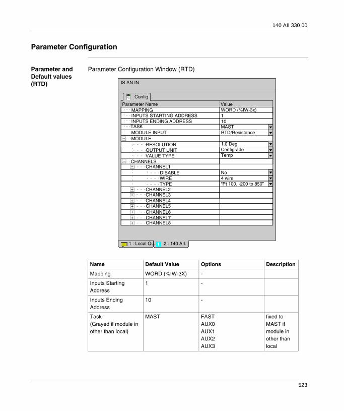
140 AII 330 00
Parameter Configuration
Parameter and Default values (RTD)
Parameter Configuration Window (RTD)
Name Default Value Options Description
Mapping WORD (%IW-3X) -
Inputs Starting Address
1 -
Inputs Ending Address
10 -
Task(Grayed if module in other than local)
MAST FASTAUX0AUX1AUX2AUX3
fixed to MAST if module in other than local
IS AN IN
Config
Parameter Name ValueMAPPING WORD (%IW-3x)
1
AUTOMATIC RESTART
1 : Local Qu... 2 : 140 AII.
CHANNELSCHANNEL1
TASK MAST
INPUTS STARTING ADDRESSINPUTS ENDING ADDRESS 10
DISABLE4 wire
CHANNEL3CHANNEL4
“Pt 100, -200 to 850”
CHANNEL5CHANNEL6CHANNEL7CHANNEL8
WIRETYPE
No
CHANNEL2
MODULERESOLUTION
VALUE TYPEOUTPUT UNIT Centigrade
Temp
1.0 Deg
MODULE INPUT RTD/Resistance
523

140 AII 330 00
Module Input RTD/Resistance TC/mV for Module Input=TC/mV see Parameter and Default values (TC), p. 525
Module
Resolution 1.0 Deg 0.1 Deg
Output Unit Centigrade Fahrenheit
Value Type Temp Raw Value
Channel1
Disable No Yes
Wire 4 wire 2 wire3 wire
Type "Pt 100, -200 to 850" "Pt 200, -200 to 850""Pt 500, -200 to 850""Pt 1000, -200 to 850""Ni 100, -200 to 850""Ni 200, -200 to 850""Ni 500, -200 to 850""Ni 1000, -200 to 850""R, 0 to 766,66 ohms""R, 0 to 4000 ohms""Apt 100, -100 to 450 ohms""Apt 200, -100 to 450 ohms""Apt 500, -100 to 450 ohms""Apt 1000, -100 to 450 ohms"
Channel2-Channel8 see Channel1
Name Default Value Options Description
524

140 AII 330 00
Parameter and Default values (TC)
Parameter Configuration Window (TC)
Name Default Value Options Description
Module Input RTD/Resistance TC/mV for Module Input=RTD/Resistance see Parameter and Default values (RTD), p. 523
Module
Resolution 1.0 Deg 0.1 Deg
Output Unit Centigrade Fahrenheit
Cold Junction Compensator On board Channel 1
Channel1
Not installed No Yes
IS AN IN
Config
Parameter Name ValueMAPPING WORD (%IW-3x)
1
AUTOMATIC RESTART
1 : Local Qu... 2 : 140 AII.
CHANNELSCHANNEL1
TASK MAST
INPUTS STARTING ADDRESSINPUTS ENDING ADDRESS 10
NOT INSTALLED25
CHANNEL3CHANNEL4
No
CHANNEL5CHANNEL6CHANNEL7CHANNEL8
RAW OUTPUT AMPLIFIEROPEN CIRCUIT TEST
No
CHANNEL2
MODULERESOLUTION
COLD JUNCTION COMP..OUTPUT UNIT Centigrade
On Board
1.0 Deg
MODULE INPUT TC/mV
UndefinedTYPE
525

140 AII 330 00
Raw Output Amplifier 25 100
Open Circuit Test No Yes
Type Undefined J, Gain=25K, Gain=25E, Gain=25T, Gain=100S, Gain=100R, Gain=100B, Gain=100
Channel2-Channel8 see Channel1
Name Default Value Options Description
526

52
140 AII 330 10: Safe Analog IN ModuleOverview
Purpose The following chapter provides information of the Quantum 140 AII 330 10 Module.
What's in this Chapter?
This chapter contains the following topics:
Topic Page
Presentation 528
Indicators 529
Wiring Diagrams 530
Specifications 536
Addressing 537
Parameter Configuration 539
527
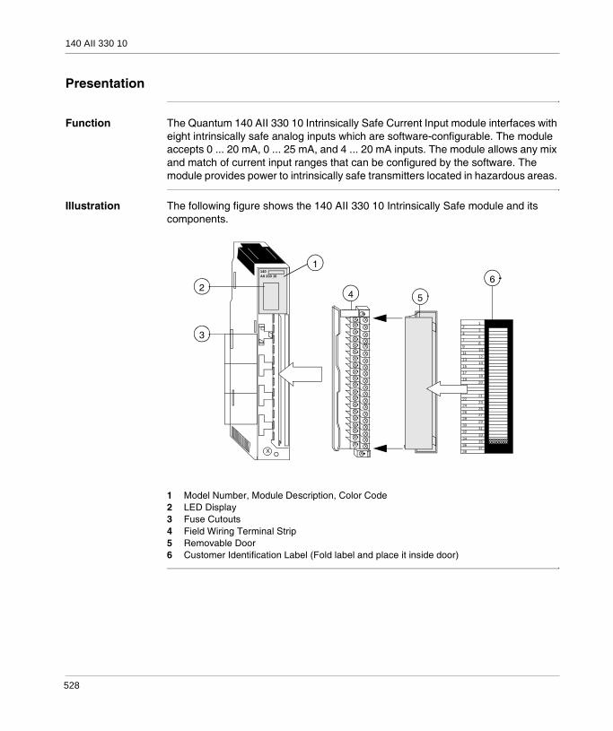
140 AII 330 10
Presentation
Function The Quantum 140 AII 330 10 Intrinsically Safe Current Input module interfaces with eight intrinsically safe analog inputs which are software-configurable. The module accepts 0 ... 20 mA, 0 ... 25 mA, and 4 ... 20 mA inputs. The module allows any mix and match of current input ranges that can be configured by the software. The module provides power to intrinsically safe transmitters located in hazardous areas.
Illustration The following figure shows the 140 AII 330 10 Intrinsically Safe module and its components.
1 Model Number, Module Description, Color Code2 LED Display3 Fuse Cutouts4 Field Wiring Terminal Strip5 Removable Door6 Customer Identification Label (Fold label and place it inside door)
140AII 330 10
X X
XXXXXXXXXXXXXXXXXXXX
XXXXXXXXXXXXXXXXXXXXX
23
6
8
10
1214
16
18
20
21
232527
29
31
3335
37
1
4
7
9
11
13
1517
19
22
24
26
28
30
32
34
3638
1
2
3
4 5
6
528

140 AII 330 10
Indicators
Illustration The following table shows the LED indicators for the 140 AII 330 10 module.
Descriptions The following table shows the LED descriptions for the 140 AII 330 10 module.
Active F
123
4
567
8
LEDs Color Indication When On
Active Green Communicating with the PLC
F Red A broken wire (4 ... 20 mA, only) or out-of-range condition on any channel
1 .. 8 Red A broken wire or out-of-range condition on the indicated channel
529

140 AII 330 10
Wiring Diagrams
Cenelec Approved Wiring Diagrams
The following is a Cenelec certified wiring diagram for the 140 AII 330 10 instrinsically safe current input module.
V1 (-) V1 (+)
N/C Signal 1
N/C Signal 2
N/C N/C
V3 (-) V3 (+)
N/C Signal 3
N/C Signal 4
N/C N/C
V5 (-) V5 (+)
N/C Signal 5
N/C Signal 6
N/C N/C
V7 (-) V7 (+)
N/C Signal 7
N/C Signal 8
N/C N/C
NON-HAZARDOUS LOCATION HAZARDOUS LOCATIONZONE 1GROUP IIA, IIB, IIC
(SEE NOTE 1)
Note 1. Only shielded twisted paircables should be used for connec-tions. Shields should be left open atthe field end and connected tochassis ground at the groundscrews on the backplane.
Note 2. A dropping resistor 100Ohms is across the signal and V(-)
Note 3. Three wire transmittersshould be provided power onlyfrom the module. An external
I.S. Module AII 330 10Blue Terminal Strip
CENELEC CERTIFICATIONEntity Parametersper Channel:Vo = 23.8 VdcIo = 112 mA/chPo = 622 mW/chCo = 127 nf/chLo = 2.9 mH/ch
V2 (-) V2 (+)
V4 (-) V4 (+)
V6 (-) V6 (+)
V8 (-) V8 (+)
(SEE NOTE 1)
I.S. 3 WIRETRANSMITTER
I.S. 2 WIRETRANSMITTER
pins of each channel. V(-) is internally connected to I.S. ground.
power supply should not be used.
Note 4. Pins marked “N/C” (NotConnected) are not electronically connected to the module.
I.S. + 14.5 Vdc
31001363 Rev 00 140 AII 330 10 Wiring Diagram
530

140 AII 330 10
CSA Approved Wiring Diagram
The following is a CSA certified wiring diagram for this module.
V1 (-) V1 (+)
N/CSignal 1
N/C Signal 2
N/C N/C
V3 (-) V3 (+)
N/C Signal 3
N/C Signal 4
N/C N/C
V5 (-) V5 (+)
N/C Signal 5
N/C Signal 6
N/C N/C
V7 (-) V7 (+)
N/C Signal 7
N/C Signal 8
N/C N/C
NON-HAZARDOUS LOCATION HAZARDOUS LOCATIONZONE 1GROUP IIA, IIB, IIC
(SEE NOTE
Note 1. Only shielded twisted paircables should be used forconnections. Shields should beleft open at the field end and connected to chassis ground at theground screws on the backplane.
Note 2. A dropping resistor 100Ohms is across the signal and V(-)
Note 3. Three wire transmittersshould be provided power onlyfrom the module. An external
I.S. Module AII 330 10Blue Terminal Strip
V2 (-) V2 (+)
V4 (-) V4 (+)
V6 (-) V6 (+)
V8 (-) V8 (+)
(SEE NOTE
I.S. 3 wiretransmitter
I.S. 2 wiretransmitter
pins of each channel. V(-) is internally connected to I.S. ground.
power supply should not be used.
Note 4. Pins marked “N/C” (NotConnected) are not electronically connected to the module.
I.S. + 14.5 Vdc(See Note 2)
ChassisGround(See Note 1)
ChassisGround(See Note 1)
Note 5. Only Quantum140 XBP 0X 00 backplanesshould be used for mounting thismodule.
Notes related toCSA certificationfor this module.
Note 2. Maximum non-hazardous area voltage must not exceed 250 V.
Note 4. Install in accordance with the NEC (ANSI/NFPA 70) and ANSI/ISA RP 12.6 for installation in the United States.Note 5. To maintain intrinsic safety, shield for each cable must be grounded and must extend as close to the terminals as possible.
Note 7. I.S. devices when connected to I.S. termi-nals must satisfy the fol-lowing conditions:Voc < VmaxIsc < ImaxCa > Ci + CcableLa > Li + Lcable
31001363 Rev 00 140 AII 330 10 Wiring Diagram
Note 8. This module is certified as a component for mounting in a suitable enclosure where the suit-ability of the final combi-nation is subject to acceptance by CSA or an inspection authority hav-ing the jurisdiction.
Note 1. Entity parameters per channel:
Voc = 23.8 VIsc = 112 mACa = 127nfLa = 1.0 mH
Note 3. Install in accordance with Canadian Electrical Code, Part I for installa-tion in Canada.
Note 6. intrinsically Safe (I.S.) cables of onemodule must be routed separately from I.S. cables of another module.
531

140 AII 330 10
FM Approved Wiring Diagrams
The following is a FM certified wiring diagram for this module.
532

140 AII 330 10
V1 (-) V1 (+)
N/C Signal 1
N/C Signal 2
N/C N/C
V3 (-) V3 (+)
N/C Signal 3
N/C Signal 4
N/C N/CV5 (-) V5 (+)
N/C Signal 5
N/C Signal 6
N/C N/C
V7 (-) V7 (+)
N/C Signal 7
N/C Signal 8
N/C N/C
HAZARDOUS LOCATION
Class I Div I Group A, B, C, DClass II Div I Group E, F, G
I.S. Module AII 330 10Blue Terminal Strip
V2 (-) V2 (+)
V4 (-) V4 (+)
V6 (-) V6 (+)
V8 (-) V8 (+)
I.S. 3 wiretransmitter
I.S. 2 wiretransmitter
I.S. + 14.5 Vdc @ 25 mA
Note 1. Only shielded cables should be used for connections. Shields should be left open at the field end and connected to chassis ground at the Module end.Note 2. Pins marked N/C are not electronically connected tothe Module.Note 3. Only 140 XBP 0xx 00 backplanes should be used formounting this module.
Note 5. The Entity Concept allows interconnection of intrinsicallysafe apparatus with associated apparatus not specificallyexamined in combination as a system when the approved valuesof Voc and Isc for the associated apparatus are less than orequal to Vmax and Imax for the intrinsically safe apparatus andthe approved values of Ca and La for the associated apparatusmust be equal to or are greater than Ci and Li for the intrinsicallysafe apparatus plus all cable parameters.
Ca ≥ Ci + Ccable; La ≥ Li + Lcable; Voc ≤ Vmax; Isc ≤ ImaxNote 6. Simple Apparatus is defined as a device which will neither generate nor store more than 1.2V, 0.1A, 20uJ, or 25 mW.For examples, switches, Thermocouples, LEDs and RTDs, etc.Note 7. Wiring methods must be in accordance with NationalElectrical Code NFPA 70, Article 504 and ANSI/ISA RP 12.6“Wiring Practices for Hazardous (classified) Locations Instrumentation Part I: Intrinsic Safety.”Note 8. Control room equipment connected to associatedapparatus should not use or generate more than 250 Vrms.Note 9. All modules must be installed in an enclosure that meetsthe requirements of ANSI/ISA S82.01.Note 10. No revision to this drawing without prior FMRC approval.
Note 4. Three wire transmitters should be provided power only from the Module. External Power Supply should not be used.
Note 11. For Schneider Electric internal use only. For control sheet,refer to 19-100986 Rev 1.
Class III Div I
ChassisGround
ChassisGround
31001363 Rev 01140 AII 330 10 Wiring Diagram
HAZARDOUS LOCATION,Class I, Div 2 Group A, B, C, D
Note 12. For Division 2 installation, the apparatus shall be installed incompliance with the enclosure, mounting, spacing, and segregation requirements of the ultimate application, includingaccess only by the use of a tool and provision for Division 2 wiringmethods.
Notes Related to FM CertificationThis IS field device should meet note 6 or should be FM approved with entity concept in Note 5 appropriate forconnection with IS Analog Current IN Module with Concept Parameters listed below. The entity parameters are per channel.Voc = 23.8 VDCIsc = 112 mA/ChCa = 127 nf/CHLa = 2.9 mH/ChPo = 622 mW/CH
533

140 AII 330 10
UL Approved Wiring Diagram
The following is a UL certified wiring diagram for this module.
V1 (-) V1 (+)
N/CSignal 1
N/CSignal 2
N/C N/C
V3 (-) V3 (+)
N/CSignal 3
N/C Signal 4
N/C N/CV5 (-) V5 (+)
N/C Signal 5
N/CSignal 6
N/C N/C
V7 (-) V7 (+)
N/C Signal 7
N/CSignal 8
N/C N/C
NON-HAZARDOUS LOCATION HAZARDOUS LOCATIONCLASS I, DIVISION I GROUP A, B, C, D
(SEE NOTE 1)
I.S. Module AII 330 10Blue Terminal Strip
V2 (-) V2 (+)
V4 (-) V4 (+)
V6 (-) V6 (+)
V8 (-) V8 (+)
(SEE NOTE 1)
I.S. 3 wiretransmitter
I.S. 2 wiretransmitter
I.S. + 14.5 Vdc
Note 1. Only shielded twisted paircables should be used forconnections. Shields should beleft open at the field end andconnected to chassis ground atthe ground screws on the backplane.
Note 4. Pins marked “N/C” (NotConnected) are not electronicallyconnected to the module.
Note 5. Only Quantum140 XBP 0X 00 backplanes shouldbe used for mounting this module along
Notes related toUL certificationfor this module.
Note 1. Entity parameters perchannel: Vcc = 24.3 V
Isc = 112 mACa = 127 nfLa = 1.5 mH
Note 2. Maximum non-hazardous area voltage mustnot exceed 250 V.
Note 3. If the electrical parametersof the cable are unknown, thefollowing values must be used
Note 4. Install in accordancewith the NEC (ANSI/NFPA 70)and ANSI/ISA RP 12.6 forinstallation in the United States.
Note 5. To maintain intrinsicsafety, shield for each cablemust be grounded and mustextend as close to the terminalsas possible.
Note 6. Intrinsically Safe (I.S)cables of one module must berouted separately from I.S.cables of another module.
Note 7. I.S. devices whenconnected to I.S. terminals must
La > Li + Lcable
Ca > Ci + Ccable
Isc < I max
Vcc < V max
satisfy the following conditions:
Note 2. A dropping resistor of 100Ohms is across the Signal and V
with the following UL listed modules:140 CPU xxx xx140 CPS xxx xx
for Ccable and Lcable:Capacitance 60Pf/ftInductance 0.20 uH/ft
(-) pins of each channel. V (-) isinternally connected to I.S. ground.
Note 3. Three Wire Transmitters should be provided power onlyfrom the module. An externalpower supply should not be used.
(See Note 2)
31001363 Rev 00 140 AII 330 10 Wiring Diagram
534

140 AII 330 10
Field Wiring Field wiring to the module consists of separate shielded, twisted pair wires. The acceptable field wire gauge is AWG 20 to AWG 12. Wiring between the module and the intrinsically safe field device should follow intrinsically safe wiring practices to avoid the transfer of unsafe levels of energy to the hazardous area.
Fixed Wiring System
The Quantum 140 AII 330 10 Intrinsically Safe Current Input module is designed with a fixed wiring system, where the field connections are made to a 40-pin, fixed position, blue terminal strip which is plugged into the module.
Terminal Strip Color and Keying Assignment
The module’s 140 XTS 332 00 field wiring terminal strip is color-coded blue to identify it as an intrinsically safe connector.
The terminal strip is keyed to prevent the wrong connector from being applied to the module. The keying assignment is given below.
Module Class Module Part Number Module Coding Terminal Strip Coding
Intrinsically Safe 140 AII 330 10 CEF ABD
535

140 AII 330 10
Specifications
General Specifications
Specifications for the Quantum 140 AII 330 10 Intrinsically Safe Current Input module are as follows.
Number of Channels 8 IN
Current Input
Linear Measuring Range 4 ... 20 mA0 ... 20 mA0 ... 25 mA
Absolute Maximum Input 25 mA internally limited
Input Impedance 100 ohms +/- 0.1% between V+ and signal terminals
Resolution 4 ... 20 mA, 0 to 4,095 counts4 ... 20 mA0 to 16,000 counts 0 ... 20 mA, 0 to 20,000 counts0 ... 25 mA, 0 to 25,000 counts
Available Voltage Terminals V+, V-, :~ 14.5 Vdc at 25 mA Terminals V+, Signal :~ 13.6 Vdc at 20 mA
Accuracy Error @ 25°C Typical: +/- 0.05% of full scale Maximum: +/- 0.1% of full scale
Linearity + 0.003% of full scale
Accuracy Drift w/ Temperature Typical: +/- 0.0025% of full scale /°CMaximum: +/- 0.005% of full scale /°C
Common Mode Rejection > 100 dB @ 50/60 Hz
Input Filter Single pole low pass, -3 dB cutoff @ 15 Hz, +/- 20%
Isolation
Channel to Channel None
Channel to Bus 1780 Vac @ 47-63 Hz or 2500 Vdc for 1 min.
Update Time 750 ms for all channels
Fault Detection Broken wire (4 ... 20 mA mode)
Bus Current Required 1.5 A
Power Dissipation 7.5 W
External Power Not required
Hot Swap Not allowed per intrinsic safety standards
Fusing Internal-not user accessible
536

140 AII 330 10
Addressing
Flat Addressing This module requires nine contiguous, 16-bit input words (%IW)—eight for input data and one for channel status. The data words formats are as follows.
The following shows the word 9 register.
Note: The word 9 register is the status of input channels. This status work for all configurations beginning PV04 and for any version (PV) with configuration 4... 20 mA. But the status don’t work for PV<04 with configurations 0...20 mA or 0...25 mA.
Channel 1 data Word 1
Word 8 Channel 8 data
15 14 13 12 11 10 9 6 5 4 3 2 1 08 7
1 = Broken wire or Out of range on channel 11 = Broken wire or Out of range on channel 2
1 = Broken wire or Out of range on channel 31 = Broken wire or Out of range on channel 4
1 = Broken wire or Out of range on channel 51 = Broken wire or Out of range on channel 6
1 = Broken wire or Out of range on channel 7
1 = Broken wire or Out of range on channel 8
537

140 AII 330 10
Topological Addressing
Topological addresses for the 140AII03010 Input Module:
Used abbreviations: b = bus, e = equipment (drop), r = rack, m = module slot.
IODDT The 140AII03010 Input Module uses the T_ANA_IN_VE IODDT:
Used abbreviations: r = rack, m = module slot, c = channel, b = bus, e = equipment (drop).
Bus and Drop default to 1 if not specified and can be left off.
I/O Map Status Byte
The I/O map status byte is used by the 140AII03010 Input Module as follows.
Point I/O Object Comment
Input 1 %IW[\b.e\]r.m.1 Value
%I[\b.e\]r.m.1.1 Broken wire or Out of range
• • •
Input 8 %IW[\b.e\]r.m.8 Value
%I[\b.e\]r.m.8.1 Broken wire or Out of range
Status Word %IW[\b.e\]r.m.9 Status of input channels
IODDT Name Object Data Type Name
T_ANA_IN_VE %CH[\b.e\]r.m.c ANA_IN_VWE userdefined
%IWr.m.c.0 Int .VALUE
%Ir.m.c.1 Bool .ERROR
Note: In Quantum IODDTs for analog modules and expert modules the data type Bool is used for %I and %Q.
12345678
MSB LSB
1 = Broken wire on one or more input channels
538

140 AII 330 10
Parameter Configuration
Parameter and Default values
Parameter Configuration Window
Name Default Value Options Description
Mapping WORD (%IW-3X) -
Inputs Starting Address
1 -
Inputs Ending Address
9 -
Task(Grayed if module in other than local)
MAST FASTAUX0AUX1AUX2AUX3
fixed to MAST if module in other than local
Channels
CH1 Range "4 ... 20 mA, 0-16000" "0... 25 mA, 0-25000""0 ... 20 mA, 0-20000""4 ... 20 mA, 0-4095"
IS AN IN 8CH CURR
Config
Parameter Name ValueMAPPING WORD (%IW-3x)
1
AUTOMATIC RESTART
1 : Local Qu... 2 : 140 AII 3
CHANNELSCH1 RANGE
TASK MAST
INPUTS STARTING ADDRESSINPUTS ENDING ADDRESS 9
CH2 RANGECH3 RANGECH4 RANGECH5 RANGECH6 RANGECH7 RANGECH8 RANGE
“4 ... 20 mA, 0-16000”“4 ... 20 mA, 0-16000”“4 ... 20 mA, 0-16000”“4 ... 20 mA, 0-16000”“4 ... 20 mA, 0-16000”“4 ... 20 mA, 0-16000”“4 ... 20 mA, 0-16000”“4 ... 20 mA, 0-16000”
539

140 AII 330 10
CH2 Range-CH8 Range
see CH1 Range
Name Default Value Options Description
540

53
140 AIO 330 00: Safe Analog OUT ModuleOverview
Purpose The following chapter provides information of the Quantum 140 AIO 330 00 Module.
What's in this Chapter?
This chapter contains the following topics:
Topic Page
Presentation 542
Indicators 543
Wiring Diagrams 544
Specifications 550
Addressing 551
Parameter Configuration 552
541

140 AIO 330 00
Presentation
Function The Quantum 140 AIO 330 00 Intrinsically Safe Analog Output module controls and monitors current loops in intrinsically safe applications. The module provides 8 dual-ended output channels that are referenced over sense resistors to a single Common. The output ranges are 4 ... 20 mA, 0 ... 20 mA, and 0 ... 25 mA. This module detects broken wires on a per-channel basis indicates their location on the front panel LEDs, and transmits the status to the PLC.
Illustration The following figure shows the140 AIO 330 00 module and its components.
1 Model Number, Module Description, Color Code2 LED Display3 Fuse Cutouts4 Field Wiring Terminal Strip5 Removable Door6 Customer Identification Label (Fold label and place it inside door)
140AIO 330 00
X X
XXXXXXXXXXXXXXXXXXXX
XXXXXXXXXXXXXXXXXXXXX
23
6
8
10
1214
16
18
20
21
232527
29
31
3335
37
1
4
7
9
11
13
1517
19
22
24
26
28
30
32
34
3638
1
2
3
4 5
6
542
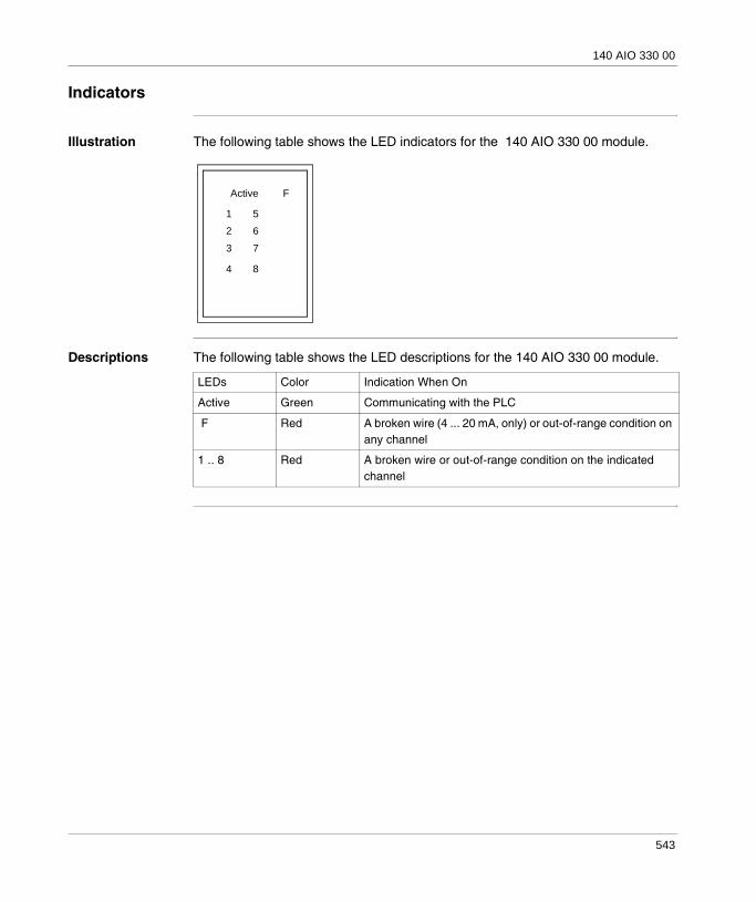
140 AIO 330 00
Indicators
Illustration The following table shows the LED indicators for the 140 AIO 330 00 module.
Descriptions The following table shows the LED descriptions for the 140 AIO 330 00 module.
Active F
123
4
567
8
LEDs Color Indication When On
Active Green Communicating with the PLC
F Red A broken wire (4 ... 20 mA, only) or out-of-range condition on any channel
1 .. 8 Red A broken wire or out-of-range condition on the indicated channel
543

140 AIO 330 00
Wiring Diagrams
CSA Approved Wiring Diagram
The following is a CSA certified wiring diagram for this module.
Output 1 (-) Monitor 1 (-)
N/COutput 1(+)
Output 2 (-) Monitor 2 (-)
N/COutput 3 (-) Monitor 3 (-)
N/C
Output 4 (-) Monitor 4 (-)
N/C
N/C N/C
N/C N/C
N/C N/COutput 5 (-)
Output 5 (+)N/C
Output 6 (-)
Output 6 (+)N/C
Output 7 (-)
Output 7 (+)N/C
Output 8 (-)
Output 8 (+)N/C
N/C
I.S. Module AIO 330 00Blue Terminal Strip
ChassisGround
HAZARDOUS LOCATIONCLASS 1, DIVISION 1GROUP A, B, C, D
(SEE NOTE 1)
I.S. Field DeviceR-500 OHMS Max
NON-HAZARDOUS LOCATION
Note 1. Only shielded cablesshould be used for connections.Shields should be left open at the field end and connected to chassis ground at the module
Note 5. Pins marked “N/C” (NotConnected) are not electronically
end.
connected to the module.
Note 6. Only Quantum140 XBP 0X 00 backplanesshould be used for mountingthis module.
Notes related toCSA certificationfor this module.
Note 1. Entity parameters perchannel: Vcc = 29.42 V
Isc = 93 mACa = 71 nfLa = 2.0 mH
Note 2. Maximum non-hazardous area voltage mustnot exceed 250 V.
Note 3. Install in accordancewith Canadian Electrical Code,Part I for installation in Canada.
Note 4. Install in accordancewith the NEC (ANSI/NFPA 70)and ANSI/ISA RP 12.6 forinstallation in the United States.
Note 5. To maintain intrinsicsafety, shield for each cablemust be grounded and mustextend as close to the terminalsas possible.
Note 6. Intrinsically Safe (I.S.)cables of one module must berouted separately from I.S.cables of another module.
Note 7. I.S. devices whenconnected to I.S. terminals mustsatisfy the following conditions:Vcc < VmaxIsc < ImaxCa > Ci + CcableLa > Li + Lcable
Note 8. This module is certifiedas a component for mounting ina suitable enclosure where thesuitability of the finalcombination is subject toacceptance by CSA or aninspection authority having thejurisdiction.
Output 2 (+)
N/C
Output 3 (+)
Output 4 (+)
Monitor 5 (-)
Monitor 6 (-)
Monitor 7 (-)
Monitor 8 (-)
V
(SEE NOTE 2)
Note 2. More than one devicecan be connected as long asthey have differential input andtotal input resistance is lessthan 500 ohms.
Note 3. The voltmeter isoptional and reads voltageproportional to the current.Length of wiring to this terminal is limited to 1 Meter.
Note 4. Unused channels willshow open loop unless outputsare shorted as shown forchannel 8.
(See Note 3)
140 AIO 330 00 Wiring Diagram31001364 Rev 00
544

140 AIO 330 00
FM Approved Wiring Diagram
The following is a FM certified wiring diagram for this module.
545

140 AIO 330 00
Output 1 (-) Monitor 1 (-)
N/COutput 2 (-)
Output 1 (+)
N/COutput 3 (-)
Output 2 (+)
N/COutput 4 (-)
N/C
N/C N/C
N/C N/C
N/C N/C
Output 5 (-)
Output 5 (+)N/C
Output 6 (-)
Output 6 (+)N/C
Output 7 (-)
Output 7 (+)
Output 8 (+)
N/C
I.S. ModuleTerminal Strip
ChassisGround
HAZARDOUS LOCATIONCLASS I DIV I GROUP A, B, C, DCLASS II DIV I GROUP E, F, G
I.S. Field DeviceR-500 OHMS Max
Note 1. Only shielded cables should be used for connections. Shields should
Note 3. Use only 140 XBP 0xx 00 backplanes to mount this module.
Note 6. The Entity Concept allows interconnection of intrinsically safeapparatus with associated apparatus not specifically examined incombination as a system when the approved values of Voc andIsc for the associated apparatus are less than or equal to Vmax and
CLASS III DIV I
be left open at the field end and connected to chassis ground at themodule end. Note 2. Pins marked “N/C” are not electronically connected to the module.
Imax for the intrinsically safe apparatus and the approved values ofCa and La for the associated apparatus must be equal to or aregreater than Ci and Li for the intrinsically Safe apparatus plus allcable parameters.Ca Š Ci + Ccable ; La Š Li + Lcable ; Voc £ Vmax ; Isc £ ImaxNote 7. Simple Apparatus is defined as a device which will neither generate
nor store more than 1.2V, 0.1A, 20mJ, or 25 mW. For example:switches, thermocouplers, LEDs, RTDs, etc. Note 8. Wiring methods must be in accordance with National Electrical
Code NFPA 70, Article 504 and ANSI/ISA RP12.6, “Wiring Practicesfor Hazardous (classified) Locations Instrumentation,Part I: Intrinsic Safety.”
Note 9. Control room equipment connected to associated apparatusshould not use or generate more than 250 Vrms.Note 10. All modules must be installed in an enclosure that meets therequirements of ANSI / ISA S82.01Note 11. No revisions to this drawing without prior FMRC Approval.
Notes Related to FM Certification
Monitor 2 (-)
Monitor 3 (-)
Output 3 (+)
Monitor 4 (-)
Output 4 (+)
Monitor 5 (-)
Monitor 6 (-)
Monitor 7 (-)
Monitor 8 (-)N/C
Output 8 (-)
N/C
N/C
Note 4. More than one device can be connected in serieS, as long as
they have differential input and total load resistance is lessthan 500 ohms.Note 5. Voltmeter is an optional Voltmeter shown to read voltage
proportional to the current. Wiring to this terminal is limitedto 1 meter.Unused channels will show Open Loop unless shorted asShown in Channel 8.
V
HAZARDOUS LOCATION,Class I, Div 2 Group A, B, C, D
Note 13. For Division 2 installation, the apparatus shall be installed in140 AIO 330 00 Wiring Diagram
31001364 Rev 01 requirements of the ultimate application, including access only by the useof a tool and provision for Division 2 wiring methods.
compliance with the enclosure, mounting, spacing, and segregation
This IS field device should meet Note 7 or should be FM approved with entity concept in Note 6 appropriate forconnection with IS RTD/TC IN Module with concept parameters listed below. The entity parameters listed are per channel.
Voc = 29.5 VDCIsc = 94 mA/ChCa = 68 nf/ChLa = 4.2 mH/ChPo = 520 mW/Ch
Note 12. For Schneider Electric internal use only. For control sheet, referto 19-100986 Rev 1.
546

140 AIO 330 00
UL Approved Wiring Diagrams
The following is a UL certified wiring diagram for this module.
Output 1 (-) Monitor 1 (-)
N/COutput 1(+)
Output 2 (-) Monitor 2 (-)
N/C
Output 3 (-) Monitor 3 (-)
N/C
Output 4 (-) Monitor 4 (-)
N/C
N/C N/C
N/C N/C
N/C N/C
Output 5 (-)
Output 5 (+)N/C
Output 6 (-)
Output 6 (+)N/C
Output 7 (-)
Output 7 (+)N/C
Output 8 (-)
Output 8 (+)N/C
N/C
I.S. Module AIO 330 00Blue Terminal Strip
ChassisGround
HAZARDOUS LOCATIONCLASS 1, DIVISION 1GROUP A, B, C, D
(SEE NOTE 1)
I.S. Field DeviceR-500 OHMS Max
NON-HAZARDOUS LOCATION
Note 1. Only shielded cablesshould be used for connections.Shields should be left open at the field end and connected to chassis ground at the module
Note 5. Pins marked “N/C” (NotConnected) are not electronically
end.
connected to the module.
Note 6. Only Quantum140 XBP 0X 00 backplanesshould be used for mountingthis module along with the
Notes related toUL certificationfor this module.
Note 1. Entity parameters perchannel: Vcc = 29.5 V
Isc = 93 mACa = 68 nfLa = 2.0 mH
Note 2. Maximum non-hazardous area voltage mustnot exceed 250 V.
Note 4. Install in accordancewith the NEC (ANSI/NFPA 70)and ANSI/ISA RP 12.6 forinstallation in the United States.
Note 5. To maintain intrinsicsafety, shield for each cablemust be grounded and mustextend as close to the terminalsas possible.
Note 6. Intrinsically Safe (I.S.)cables of one module must berouted separately from I.S.cables of another module.
Note 7. I.S. devices whenconnected to I.S. terminals mustsatisfy the following conditions:Vcc < VmaxIsc < ImaxCa > Ci + CcableLa > Li + Lcable
Output 2 (+)
N/C
Output 3 (+)
Output 4 (+)
Monitor 5 (-)
Monitor 6 (-)
Monitor 7 (-)
Monitor 8 (-)
V
(SEE NOTE 2)
Note 2. More than one devicecan be connected as long asthey have differential input andtotal input resistance is lessthan 500 ohms.
Note 3. The voltmeter isoptional and reads voltageproportional to the current.Length of wiring to this terminal is limited to 1 Meter.
Note 4. Unused channels willshow open loop unless outputsare shorted as shown forchannel 8.
(See Note 3)
following UL listed modules:140 CPU xxx xx140 CPS xxx xx
Note 3. If the electricalparameter of the cable areunknown, the following valuesmust be used for Ccable andLcable:
Capacitance 60 Pf/ftInductance 0.20 uH/ft
140 AIO 330 00 Wiring Diagram31001364 Rev 00
547

140 AIO 330 00
Cenelec Approved Wiring Diagram
The following is a Cenelec certified wiring diagram for this module.
Output 1 (-) Monitor 1 (-)
N/COutput 1(+)
Output 2 (-) Monitor 2 (-)
N/C
Output 3 (-) Monitor 3 (-)
N/C
Output 4 (-) Monitor 4 (-)
N/C
N/C N/C
N/C N/C
N/C N/COutput 5 (-)
Output 5 (+)N/C
Output 6 (-)
Output 6 (+)N/C
Output 7 (-)
Output 7 (+)N/C
Output 8 (-)
Output 8 (+)N/C
N/C
I.S. Module AIO 330 00Blue Terminal Strip
ChassisGround
HAZARDOUS LOCATIONCLASS 1, DIVISION 1GROUP A, B, C, D
(SEE NOTE 1)
I.S. Field DeviceR-500 OHMS Max
NON-HAZARDOUS LOCATION
Note 1. Only shielded cablesshould be used for connections.Shields should be left open at the field end and connected to chassis ground at the module
Note 5. Pins marked “N/C” (NotConnected) are not electronically
end.
connected to the module.
CENELEC CERTIFICATIONEntity Parametersper channel:
Output 2 (+)
N/C
Output 3 (+)
Output 4 (+)
Monitor 5 (-)
Monitor 6 (-)
Monitor 7 (-)
Monitor 8 (-)
V
(SEE NOTE 2)
Note 2. More than one devicecan be connected as long asthey have differential input andtotal input resistance is lessthan 500 ohms.
Note 3. The voltmeter isoptional and reads voltageproportional to the current.Length of wiring to this terminal is limited to 1 Meter.
Note 4. Unused channels willshow open loop unless outputsare shorted as shown forchannel 8.
(See Note 3)
Vo = 29.5 VdcIo = 94 mA/ChPo = 520 mW/chCo = 68 nf/chLo = 4.2 mH/ch
31001364 Rev 00
AIO 330 00 Wiring Diagram (Analog Output)
548
140 AIO 330 00
Field Wiring Field wiring to the module should consist of separate shielded, twisted pair wires. The acceptable field wire gauge should be AWG 30 to AWG 18. Wiring between the module and the intrinsically safe field device should follow intrinsically safe wiring practices to avoid the transfer of unsafe levels of energy to the hazardous area.
Fixed Wiring System
The Quantum140 AIO 330 00 Intrinsically Safe Analog Output module is designed with a fixed wiring system where the field connections are made to a 40-pin, fixed position, blue terminal strip which is plugged into the module.
Terminal Strip Color and Keying Assignment
The module’s 140 XTS 332 00 field wiring terminal strip is color-coded blue to identify it as an intrinsically safe connector.
The terminal strip is keyed to prevent the wrong connector from being applied to the module. The keying assignment is given below.
Module Class Module Part Number Module Coding Terminal Strip Coding
Intrinsically Safe 140 AIO 330 00 CEF ABD
549

140 AIO 330 00
Specifications
General Specifications
Specifications for the Quantum 140 AIO 330 00 Intrinsically Safe Analog Output module are as follows.
Number of Channels 8 OUT
Loop Resistance 500 ohms maximum
Ranges 4 ... 20 mA (0 to 4095) 4 ... 20 mA (0 to 16000)0 ... 20 mA (0 to 20000) 0 ... 25mA (0 to 25000)
Resolution 15 bits within 4 ... 20 mA
Accuracy Drift w/Temperature
Typical: 40 PPM/°C. Maximum: 70 PPM/°C
Accuracy Error @ 25°C +/- 0.2% of full scale
Linearity +/- 1 LSB
Isolation
Channel to Channel None
Channel to Bus 1780 VAC RMS for 1 minute
Update Time 4 ms - for all channels
Settling Time 1 ms to +/- 0.1% of the final value
Bus Current Required 2.5 Amp
Power Dissipation 12.5 W
External Power Not required for this module
Fault Detection Open circuit in 4 ... 20 mA range
Voltmeter Monitor Specifications
Range 0.250 ... 1.250 V
Scaling (Volts) = (mA) x 0.0625
Output Impedance 62.5 W Typical
Wire Length 1 m maximum
Hot Swap Not allowed per intrinsic safety standards
Fusing Internal - not user accessible
VOUT ILOOP
550

140 AIO 330 00
Addressing
Flat Addressing This module requires eight contiguous, 16-bit words (%MW) for output data. The data words formats are as follows.
Topological Addressing
Topological addresses for the 140AIO33000 Output Module:
Used abbreviations: b = bus, e = equipment (drop), r = rack, m = module slot.
I/O Map Status Byte
The I/O map status byte is used by the 140AIO33000 Output Module as follows.
Channel 1 data Word 1
Word 8 Channel 8 data
Point I/O Object Comment
Output 1 %QW[\b.e\]r.m.1 Value
Output 2 %QW[\b.e\]r.m.2 Value
• • •
Output 7 %QW[\b.e\]r.m.7 Value
Output 8 %QW[\b.e\]r.m.8 Value
Channel 1 loop broken wire
12345678
MSB LSB
Channel 2 loop broken wireChannel 3 loop broken wiree
Channel 4 loop broken wireChannel 5 loop broken wire
Channel 6 loop broken wireChannel 7 loop broken wiree
Channel 8 loop broken wire
551
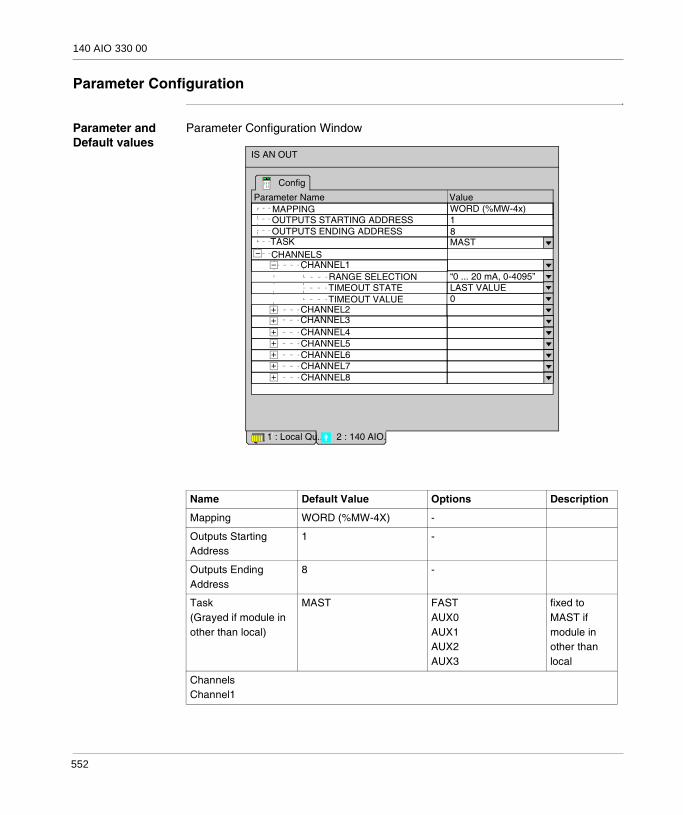
140 AIO 330 00
Parameter Configuration
Parameter and Default values
Parameter Configuration Window
Name Default Value Options Description
Mapping WORD (%MW-4X) -
Outputs Starting Address
1 -
Outputs Ending Address
8 -
Task(Grayed if module in other than local)
MAST FASTAUX0AUX1AUX2AUX3
fixed to MAST if module in other than local
ChannelsChannel1
IS AN OUT
Config
Parameter Name ValueMAPPING WORD (%MW-4x)
1
AUTOMATIC RESTART
1 : Local Qu... 2 : 140 AIO.
CHANNELSCHANNEL1
TASK MAST
OUTPUTS STARTING ADDRESSOUTPUTS ENDING ADDRESS 8
RANGE SELECTIONLAST VALUE
CHANNEL2CHANNEL3CHANNEL4
0
CHANNEL5CHANNEL6CHANNEL7CHANNEL8
TIMEOUT STATETIMEOUT VALUE
“0 ... 20 mA, 0-4095”
552

140 AIO 330 00
Range Selection "4 ... 20 mA, 0-16000" "4 ... 20 mA, 0-4095""0 ... 20 mA, 0-20000""0 ... 25 mA, 0-25000"
Timeout State DISABLED LAST VALUEUSER DEFINED
Timeout Value 0 0-65535 only enabled Timeout State=USER DEFINED
Channel2-Channel8 see Channel1
Name Default Value Options Description
553

140 AIO 330 00
554

54
140 DII 330 00: Safe Discrete IN ModuleOverview
Purpose The following chapter provides information of the Quantum 140 DII 330 00 Module.
What's in this Chapter?
This chapter contains the following topics:
Topic Page
Presentation 556
Indicators 557
Wiring Diagrams 558
Specifications 563
Parameter Configuration 564
555

140 DII 330 00
Presentation
Function The Quantum 140 DII 330 00 Intrinsically Safe Digital Input module provides safe power to dry contact closures e.g., push buttons, selector switches, float switches, flow switches, limit switches, etc., in a hazardous area, and receives the proportional current to indicate an on/off state. The received current is converted into digital signals that is transferred to the PLC.
Illustration The following figure shows the 140 DII 330 00 module and its components.
1 Model Number, Module Description, Color Code2 LED Display3 Fuse Cutouts4 Field Wiring Terminal Strip5 Removable Door6 Customer Identification Label (Fold label and place it inside door)
140DII 330 00
X X
XXXXXXXXXXXXXXXXXXXX
XXXXXXXXXXXXXXXXXXXXX
23
6
8
10
1214
16
18
20
21
232527
29
31
3335
37
1
4
7
9
11
13
1517
19
22
24
26
28
30
32
34
3638
1
2
3
4 5
6
556

140 DII 330 00
Indicators
Illustration The following table shows the LED indicators for the 140 DII 330 00 module.
Descriptions The following table shows the LED descriptions for the 140 DII 330 00 module.
Active
123
4
567
8
LEDs Color Indication When On
Active Green Bus communication is present
1 .. 8 Green The indicated point or channel is on
557
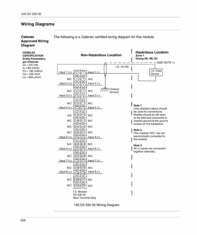
140 DII 330 00
Wiring Diagrams
Celenec Approved Wiring Diagram
The following is a Celenec certified wiring diagram for this module.
CENELEC CERTIFICATIONEntity Parametersper Channel:Vo = 9.6 VdcIo = 80 mA/chPo = 192 mW/chCo = 450 nf/chLo = 694 μH/ch
Note 1Only shielded cables should be used for connections. Shields should be left open at the field and connected to chassis ground at the ground screws on the backplane.
Note 2Pins marked "N/C" are not electronically connected to the module.
Note 3All (-) inputs are connected together internally.
Non-Hazardous LocationHazardous LocationZone 1Group IIA, IIB, IIC
(SEE NOTE 1)
I.S. FieldDevice
I.S. +8 Vdc
ChassisGround
I.S. ModuleDII 330 00Blue Terminal Strip
Input 2 (+)
Input 3 (+)
Input 4 (+)
Input 5 (+)
Input 6 (+)
Input 7 (+)
Input 8 (+)
Input 2 (-)
Input 3 (-)
Input 4 (-)
Input 5 (-)
Input 6 (-)
Input 7 (-)
Input 8 (-)
N/C
N/C
N/C
N/C
N/C
N/C
N/C
N/C
N/C
N/C
N/C
N/C
Input 1 (+) Input 1 (-)
N/C
N/C
N/C
N/C
N/C
N/C
N/C
N/C
N/C
N/C
N/C
N/C
140 DII 330 00 Wiring Diagram
558

140 DII 330 00
CSA Approved Wiring Diagram
The following is a CSA certified wiring diagram for this module.
Input 1 (+) Input 1 (-)
N/C N/CInput 2 (+) Input 2 (-)
N/C N/C
Input 3 (+) Input 3 (-)
N/C N/CInput 4 (+) Input 4 (-)
N/C N/C
N/C N/C
N/C N/C
N/C N/CInput 5 (+) Input 5 (-)
N/C N/CInput 6 (+) Input 6 (-)
N/C N/CInput 7 (+) Input 7 (-)
N/C N/CInput 8 (+) Input 8 (-)
N/C N/C
N/C N/C
I.S. ModuleDII 330 00Blue Terminal Strip
ChassisGround
HAZARDOUS LOCATIONCLASS 1, DIVISION 1GROUP A, B, C, D
(SEE NOTE 1)
I.S. FieldDevice
NON-HAZARDOUS LOCATION
I.S. +8 Vdc
31001365 Rev 00 140 DII 330 00 Wiring Diagram
Note 1Only shielded cables should be used for connections. Shields should be left open at the field and connected to chassis ground at the ground screws on the backplane.
Note 2Pins marked "N/C" are not electronically connected to the module.
Note 3Only Quantum 140 XBP oX oo backplanes should be used for mounting this module.
Notes Related to CSA Certification for this module
Note 1 Entity parameters are provided per channel:Voc = 9.5 VIsc = 80 mACa = 450 nfLa = 694 mH
Note 2 Maximum non-hazardous area voltage must not exceed 250 V.
Note 3In Canada, install in accordance with Canadian Electrical Code, Part I.
Note 4In the United States, install in accordance with the NEC (ANSI/NFPA 70) and ANSI / ISA RP 12.6.
Note 5 To maintain intrinsic safety, shield for each cable must be grounded and must extend as close to the termi-nals as possible.
Note 6 Intrinsically Safe (I.S.) cables of one module must be routed sepa-rately from I.S. cables of another module.
Note 7 I.S. devices when connected to I.S. terminals must satisfy the follow-ing conditions:Vcc < VmaxIsc < ImaxCa > Ci + CcableLa > Li + Lcable
Note 8This module is certified as a compo-nent for mounting in a suitable enclo-sure where the suitability of the final combination is subject to acceptance by CSA or an inspection authority having the juridiction.
559

140 DII 330 00
FM Approved Wiring Diagram
The following is a FM certified wiring diagram for this module.
Input 1 (+) Output 1 (-)
N/C N/CInput 2 (+) Input 2 (-)
N/C N/C
Input 3 (+) Input 3 (-)
N/C N/C
Input 4 (+) Input 4 (-)
N/C N/C
N/C N/C
N/C N/C
N/C N/CInput 5 (+) Input 5 (-)
N/C N/CInput 6 (+) Input 6 (-)
N/C N/CInput 7 (+) Input 7 (-)
N/C N/CInput 8 (+) Input 8 (-)
N/C N/C
N/C N/C
I.S. ModuleDII 330 00Blue Terminal Strip
ChassisGround
HAZARDOUS LOCATIONCLASS I DIV I GROUP A, B, C, DCLASS II DIV I GROUP E, F, G
I.S. FieldDevice
I.S. +8 VdcCLASS III DIV I
140 DII 330 00 Wiring Diagram
HAZARDOUS LOCATION,CLASS I DIV II GROUP A, B, C, D
31001365 Rev 01
Notes Related to FM CertificationThis IS field device should meet Note 5 or should be FM approved with entity concept in Note 4 appropriate for connectionwith IS RTD/TC IN Module with Concept Parameters LIsted below. The entity parameters are per Channel.Voc = 27.9 VDCIsc = 121 mA/ChCa = 84 nf/ChLa = 2.2 mH/ChPo = 840 mW/Ch
Note 1: Only shielded cables should be used for connections. Shields should be left open at the field end, and connected to chassis ground at the module end.Note 2: Pins marked "N/C" are not electronically connected to the module.Note 3: To mount modules of this type, use only 140 XBP 0xx 00 backplanes.Note 4: The Entity Concept allows interconnection of Intrinsi-cally Safe apparatus with associated apparatus not specifically examined in combination as a system when the approved values of Voc and Isc for the associated apparatus are less than or equal to Vmax and Imax for the I.S. apparatus, and the approved values of Ca and La for the associated apparatus must be equal to or greater than Ci and Li for the I.S. apparatus, plus all cable parameters.Ca > Ci + Ccable ; La > Li + Lcable ; Voc < Vmax ; lsc < ImaxNote 5: Simple apparatus is defined as a device which will nei-ther generate nor store more than 1.2 V, 0.1 A, 20 mJ, or 25 mW; for example: switches, thermocouplers, LEDs, RTDs, etc. mount modules of this type, use only 140 XBP 0xx 00 backplanes.Note 6: Wiring methods must be in accordance with National Electrical Code NFPA 70, Article 504 and ANSI/ISA RP12.6, “Wir-ing Practices for Hazardous (classified) Locations Instrumenta-tion, Part I: Intrinsic Safety.” Note 7: Control room equipment connected to associated apparatus should not use or generate more than 250 Vrms.Note 8: All modules must be installed in an enclosure that meets the requirements of ANSI/ISA S82.01.Note 9: No revision to this drawing without prior FMRC approval.Note 10: For Schneider Electric internal use only. For control sheet, refer to 19-100986 Rev. 1.Note 11: For Division 2 installation, the apparatus shall be installed in compliance with the enclosure, mounting, spacing, and segregation requirements of the ultimate application, includ-
560

140 DII 330 00
UL Approved Wiring Diagram
The following is a UL certified wiring diagram for this module.
Fixed Wiring System
The Quantum 140 DII 330 00 Intrinsically Safe Digital Input module is designed with a fixed wiring system where the field connections are made to a 40-pin, fixed position, blue terminal strip which is plugged into the module.
Input 1 (+)
N/C
Input 1(-)
Input 2 (+)
N/C
Input 3 (+)
N/C
Input 4 (+)
N/C
N/C N/C
N/C N/C
N/C N/C
Input 5 (+) Input 5 (-)
N/C
Input 6 (+) Input 6 (-)
N/C
Input 7 (+) Input 7 (-)
N/C
Input 8 (+) Input 8 (-)
N/C
N/C
I.S. Module
Blue Terminal Strip
ChassisGround
HAZARDOUS LOCATIONCLASS 1, DIVISION 1Group A, B, C, D
(SEE NOTE 1)
I.S. Field
NON-HAZARDOUS LOCATIONNotes related toUL certificationfor this module.
Note 1. Entity parameters perchannel: Voc = 27.9 V
Isc = 119 mACa = 84 nfLa = 1.0 mH
Note 2. Maximum non-hazardous area voltage mustnot exceed 250 V.
Note 4. Install in accordancewith the NEC (ANSI/NFPA 70)and ANSI/ISA RP 12.6 forinstallation in the United States.
Note 5. To maintain intrinsicsafety, shield for each cablemust be grounded and mustextend as close to the terminalsas possible.
Note 6. Intrinsically Safe (I.S.)cables of one module must berouted separately from I.S.cables of another module.
Note 7. I.S. devices whenconnected to I.S. terminals mustsatisfy the following conditions:Vcc < VmaxIsc < ImaxCa > Ci + CcableLa > Li + Lcable
Input 2 (-)
N/C
Input 3 (-)
Input 4 (-)
Note 3. If the electricalparameters of the cable areunknown, the following valuesmust be used for Ccable andLcable:
Capacitance 60 Pf/ftInductance 0.20 uH/ft
Device
I.S. +8 Vdc
N/C
N/C
N/C
N/C
N/C
N/C
N/C
N/C
DII 330 00
140 DII 330 00 Wiring Diagram31001365 Rev 01
Note 1Only shielded cables should be usedfor connections. Shields should be left open at the fieldand connected to chassis ground at the ground screws on the backplane
Note 2Pins marked "N/C" are not electroni-cally connected to the module.
Note 3Only Quantum 140 XBP oX oo back-planes should be used for mounting this module, along with the following UL-listed modules: 140 CPU xxx xx 140 CPS xxx xx
561

140 DII 330 00
Field Wiring Field wiring to the module consists of separate shielded twisted pair wires. The acceptable field wire gauge is AWG 20 to AWG 12. Wiring between the module and the intrinsically safe field device should follow intrinsically safe wiring practices, to avoid the transfer of unsafe levels of energy to the hazardous area.
Terminal Strip Color and Keying Assignment
The module’s 140 XTS 332 00 field wiring terminal strip is color-coded blue to identify it as an intrinsically safe connector.
The terminal strip is keyed to prevent the wrong connector from being applied to the module. The keying assignment is given below.
Module Class Module Part Number Module Coding Terminal Strip Coding
Intrinsically Safe 140 DII 330 00 CDE ABF
562
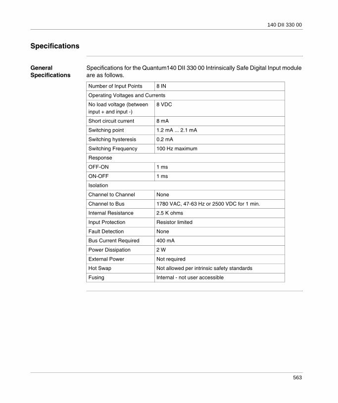
140 DII 330 00
Specifications
General Specifications
Specifications for the Quantum140 DII 330 00 Intrinsically Safe Digital Input module are as follows.
Number of Input Points 8 IN
Operating Voltages and Currents
No load voltage (between input + and input -)
8 VDC
Short circuit current 8 mA
Switching point 1.2 mA ... 2.1 mA
Switching hysteresis 0.2 mA
Switching Frequency 100 Hz maximum
Response
OFF-ON 1 ms
ON-OFF 1 ms
Isolation
Channel to Channel None
Channel to Bus 1780 VAC, 47-63 Hz or 2500 VDC for 1 min.
Internal Resistance 2.5 K ohms
Input Protection Resistor limited
Fault Detection None
Bus Current Required 400 mA
Power Dissipation 2 W
External Power Not required
Hot Swap Not allowed per intrinsic safety standards
Fusing Internal - not user accessible
563

140 DII 330 00
Parameter Configuration
Parameter and Default values
Parameter Configuration Window
Name Default Value Options Description
Mapping BIT (%I-1x) WORD (%IW-3X)
Inputs Starting Address
1 1
Inputs Ending Address
8 1
Input Type BINARY BCD
Task(Grayed if module in other than local)
MAST FASTAUX0AUX1AUX2AUX3
fixed to MAST if module in other than local
I.S. digital input
Config
Parameter Name ValueMAPPING BIT (%I-1X)INPUTS STARTING ADDRESS 1INPUTS ENDING ADDRESS 8INPUT TYPE BINARY
1 : Local Qu... 2 : 140 DDI...
TASK MAST
564

55
140 DIO 330 00: Safe Discrete OUT ModuleOverview
Purpose The following chapter provides information of the Quantum 140 DIO 330 00 Module.
What's in this Chapter?
This chapter contains the following topics:
Topic Page
Presentation 566
Indicators 567
Wiring Diagrams 568
Specification 573
140 DIO 330 00 Parameter Configuration 574
565

140 DIO 330 00
Presentation
Function The Quantum 140 DIO 330 00 Intrinsically Safe Digital Output module provides intrinsically safe power to a variety of components such as solenoid valves, LEDs, etc., located in a hazardous area. This module is for use with sink devices only.
Illustration The following figure shows the 140 DIO 330 00 module and its components.
1 Model Number, Module Description, Color Code
2 LED Display
3 Fuse Cutouts
4 Field Wiring Terminal Strip
5 Removable Door
6 Customer Identification Label (Fold label and place it inside door)
140DIO 330 00
X X
XXXXXXXXXXXXXXXXXXXX
XXXXXXXXXXXXXXXXXXXXX
23
6
8
10
1214
16
18
20
21
232527
29
31
3335
37
1
4
7
9
11
13
1517
19
22
24
26
28
30
32
34
3638
1
2
3
4 5
6
566

140 DIO 330 00
Indicators
Illustration The following table shows the LED indicators for the 140 DIO 330 00 module.
Descriptions The following table shows the LED descriptions for the 140 DIO 330 00 module.
Active
123
4
567
8
LEDs Color Indication When On
Active Green Bus communication is present
1 .. 8 Green The indicated point or channel is on
567

140 DIO 330 00
Wiring Diagrams
Celenec Approved Wiring Diagram
The following is a Celenec certified wiring diagram for this module.
CENELEC CERTIFICATIONEntity Parametersper Channel:Vo = 27.9 VdcIo = 121 mA/chPo = 840 mW/chCo = 84 nf/chLo =2.2 mH/ch
Note 1Only shielded cables should be used for connections. Shields should be left open at the field and connected to chassis ground at the module end.
Note 2Pins marked "N/C" are not electronically connected to the module.
Note 3All (-) outputs are connected together internally.
Non-Hazardous LocationHazardous LocationZone 1Group IIA, IIB, IIC
(See Notes 1 & 2)
I.S. FieldDevice
I.S. +8 Vdc
ChassisGround
I.S. ModuleDIO 330 00Blue Terminal Strip
Output 2 (+)
Output 3 (+)
Output 4 (+)
Output 5 (+)
Output 6 (+)
Output 7 (+)
Output 8 (+)
Output 2 (-)
Output 3 (-)
Output 4 (-)
Output 5 (-)
Output 6 (-)
Output 7 (-)
Output 8 (-)
N/C
N/C
N/C
N/C
N/C
N/C
N/C
N/C
N/C
N/C
N/C
N/C
Output 1 (+) Output 1 (-)
N/C
N/C
N/C
N/C
N/C
N/C
N/C
N/C
N/C
N/C
N/C
N/C
140 DIO 330 00 Wiring Diagram
568

140 DIO 330 00
CSA Approved Wiring Diagram
The following is a CSA certified wiring diagram for this module.
NON-HAZARDOUS LOCATION HAZARDOUS LOCATIONCLASS 1, DIVISION 1GROUPS A, B, C, D
I. S. FIELDDEVICE
See Notes 1 & 2
output 1(+)
output 3(-)
output 2(-)
output 4(+)
output 3(+)
output 2(+)
output 5(-)output 5(+)
output 4(-)
output 8(-)
output 7(-)
output 6(-)output 6(+)
output 7(+)
output 8(+)
output 1(-)
N/C
N/C
N/C
N/C
N/C
N/C
N/C
N/C
N/C
N/C
N/C
N/C
N/C
N/C
N/C
N/C
N/C
N/C
N/C
N/C
N/C
N/C
N/C
N/C
N/C
I. S. +24 V dc @ No Load
Note 1: Only shielded cables should be used for connections. Shields should be left open at the field and connected to chassis ground at the ground screws on the backplane.
Note 2. All negative ( - ) outputs [1 through 8] are internally connected to Intrinsically Safe ( I.S.) ground.
Note 3. Pins marked "N/C" are not electronically con-nected to the module.
Note 4. Only Quantum 140 XBP 0X 00 back-plane should be used when mounting this module.
Notes Related to CSA Certification for this module
Note 1 Entity parameters are provided per channel:Voc = 27.9 VIsc = 119 mACa = 84 nfLa = 1.0 mH
Note 2 Maximum non-hazardous area volt-age must not exceed 250 V.
Note 3In Canada, install in accordance with Canadian Electrical Code, Part I.
Note 4In the United States, install in accor-dance with the NEC (ANSI/NFPA 70) and ANSI / ISA RP 12.6.
Note 5 To maintain intrinsic safety, shield for each cable must be grounded and must extend as close to the termi-nals as possible.
Note 6 Intrinsically Safe (I.S.) cables of one module must be routed separately from I.S. cables of another module.
Note 7 I.S. devices when connected to I.S. terminals must satisfy the following conditions:Vcc < VmaxIsc < ImaxCa > Ci + CcableLa > Li + Lcable
Note 8This module is certified as a compo-nent for mounting in a suitable enclo-sure where the suitability of the final combination is subject to accep-tance by CSA or an inspection authority having the juridiction.
I.S. Module140 DIO 330 00Blue Terminal Strip
569

140 DIO 330 00
FM Approved Wiring Diagram
The following is a FM certified wiring diagram for this module.
Note 1: Only shielded cables should be used for connections. Shields should be left open at the field end, and connected to chassis ground at the module end.
Note 2: Pins marked "N/C" are not electronically connected to the module.
Note 3: To mount modules of this type, use only 140 XBP 0xx 00 backplanes.
Note 4: The Entity Concept allows interconnection of Intrin-sically Safe apparatus with associated apparatus not specif-ically examined in combination as a system when the approved values of Voc and Isc for the associated apparatus are less than or equal to Vmax and Imax for the I.S. appara-tus, and the approved values of Ca and La for the associated apparatus must be equal to or greater than Ci and Li for the I.S. apparatus, plus all cable parameters.Ca > Ci + Ccable; La > Li + Lcable; Voc < Vmax; lsc < Imax
Note 5: Simple apparatus is defined as a device which will neither generate nor store more than 1.2 V, 0.1 A, 20 mJ, or 25 mW; for example: switches, thermocouplers, LEDs, RTDs, etc. mount modules of this type, use only 140 XBP 0xx 00 back-planes.
Note 6: Wiring methods must be in accordance with National Electrical Code NFPA 70, Article 504 and ANSI/ISA RP12.6, “Wiring Practices for Hazardous (classified) Locations Instrumentation, Part I: Intrinsic Safety.”
Note 7: Control room equipment connected to associated appa-ratus should not use or generate more than 250 Vrms.
Note 8: All modules must be installed in an enclosure that meets the requirements of ANSI/ISA S82.01.
Note 9: No revision to this drawing without prior FMRC approval.
Note 10: For Schneider Electric internal use only. For control sheet, refer to 19-100986 Rev. 0.
Non-Hazardous Location
(See Notes 1 & 2)
I.S. FieldDevice
I.S. +24 VDC @ NO LOAD
ChassisGround
I.S. ModuleDIO 330 00Blue Terminal
Output 4 (+) Output 4 (-)
Output 1 (+) Output 1 (-)
N/C N/C
N/C N/C
Output 6 (+) Output 6 (-)
Output 5 (+) Output 5 (-)
Output 2 (+) Output 2 (-)
Output 7 (+) Output 7 (-)
Output 8 (+) Output 8 (-)
Output 3 (+) Output 3 (-)
N/C
N/C
N/C
N/C
N/C
N/C
N/C
N/C
N/C N/C
N/C N/C
N/C N/C
Hazardous LocationClass I Div. I Group A,B,C,DClass II Div. I Group E,F,GClass III Div. I
Notes Related to FM CertificationThis I.S. field device should meet Note 5, or be FM-approved with the Entity Concept, as oulined in Note 4, appropriate for connection with the I.S. RTD/TC IN module, with the Concept parameters listed below. Entity parameters provided are per channel.Voc = 27.9 VdcIsc = 121 mA/chCa = 84 nf/chLa = 2.2 mH/chPo = 840 mW/chN/C N/C
570

140 DIO 330 00
UL Approved Wiring Diagram
The following is a UL certified wiring diagram for this module.
Output 1 (+)
N/C
Output 1(-)
Output 2 (+)
N/C
Output 3 (+)
N/C
Output 4 (+)
N/C
N/C N/C
N/C N/C
N/C N/COutput 5 (+) Output 5 (-)
N/C
Output 6 (+) Output 6 (-)
N/C
Output 7 (+) Output 7 (-)
N/C
Output 8 (+) Output 8 (-)
N/C
N/C
I.S. Module
Blue Terminal Strip
ChassisGround
HAZARDOUS LOCATIONCLASS 1, DIVISION 1Group A, B, C, D
(See Notes 1 & 2)
I.S. Field
NON-HAZARDOUS LOCATION
.
Output 2 (-)
N/C
Output 3 (-)
Output 4 (-)
Device
I.S. +24 Vdc @ NO LOAD
N/C
N/C
N/C
N/C
N/C
N/C
N/C
N/C
140 DIO 330 00
140 DIO 330 00 Wiring Diagram31001366 Rev 00
Note 1Only shielded cables should be used for connections. Shields should be left open at the field end and con-nected to chassis ground at the ground screws on the backplane.
Note 2All negative output terminals [ Output 1 (-) thru Output 8 (-) ] are internally connected to I.S. ground.
Note 3Pins marked “N/C” (Not Connected) are not electronically connected to the module.
Note 4Only Quantum 140 XBP 0X 00 backplanes should be used for mounting this module along with the following UL listed modules: 140 CPU xxx xx 140 CPS xxx xx
Notes Related to UL Certifi-cation for this module
Note 1 Entity parameters are pro-vided per channel:Voc = 27.9 VIsc = 119 mACa = 84 nfLa = 1.0 mH
Note 2 Maximum non-hazardous area voltage must not exceed 250 V.
Note 3If the electrical parameters of the cable are unknown, the fol-lowing values must be used for Ccable and Lcable: Capacitance: 60 Pf/ft Inductance: 0.20 uH/ft
Note 4Install in accordance with the NEC (ANSI/NFPA 70) and ANSI/ISA RP 12.6 for installa-tion in the United States.
Note 5 To maintain intrinsic safety, shield for each cable must be grounded and must extend as close to the terminals as possible.
Note 6 Intrinsically Safe (I.S.) cables of one module must be routed separately from I.S. cables of another module.
Note 7 I.S. devices when connected to I.S. terminals must satisfy the following conditions:Vcc < VmaxIsc < ImaxCa > Ci + CcableLa > Li + Lcable
571

140 DIO 330 00
Fixed Wiring System
The Quantum 140 DIO 330 00 Intrinsically Safe Digital Output module is designed with a fixed wiring system where the field connections are made to a 40-pin, fixed position, blue terminal strip, which is plugged into the module.
Field Wiring Field wiring to the module consists of separate shielded, twisted pair wires. Acceptable field wire gauges go from AWG 20 to AWG 12. Wiring between the module and the intrinsically safe field device should follow intrinsically safe wiring practices, to avoid the transfer of unsafe levels of energy to the hazardous area.
Terminal Strip Color and Keying Assignment
The module’s 140 XTS 332 00 field wiring terminal strip is color-coded blue to identify it as an intrinsically safe connector.The terminal strip is keyed to prevent the wrong connector from being applied to the module. The keying assignment is given below.
Module Class Module Part Number
Module Coding
Terminal Strip Coding
Intrinsically Safe 140 DIO 330 00 CDE ABF
572
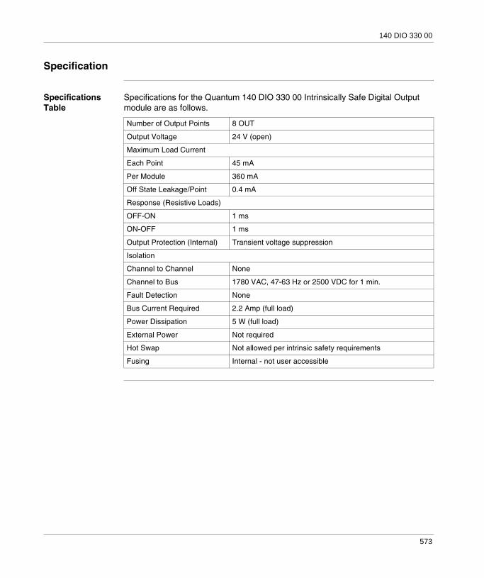
140 DIO 330 00
Specification
Specifications Table
Specifications for the Quantum 140 DIO 330 00 Intrinsically Safe Digital Output module are as follows.
Number of Output Points 8 OUT
Output Voltage 24 V (open)
Maximum Load Current
Each Point 45 mA
Per Module 360 mA
Off State Leakage/Point 0.4 mA
Response (Resistive Loads)
OFF-ON 1 ms
ON-OFF 1 ms
Output Protection (Internal) Transient voltage suppression
Isolation
Channel to Channel None
Channel to Bus 1780 VAC, 47-63 Hz or 2500 VDC for 1 min.
Fault Detection None
Bus Current Required 2.2 Amp (full load)
Power Dissipation 5 W (full load)
External Power Not required
Hot Swap Not allowed per intrinsic safety requirements
Fusing Internal - not user accessible
573

140 DIO 330 00
140 DIO 330 00 Parameter Configuration
Parameter Configuration Window
Parameter and Default Values
I.S. digital output
Config
Parameter Name ValueMAPPING BIT (%M-0X)OUTPUTS STARTING ADDRESS 1OUTPUTS ENDING ADDRESS 8
OUTPUT TYPE BINARY
1 : Local Qu... 2 : 140 DIO.
TIMEOUT STATE USER DEFINEDVALUE
TASK MAST
0
Name Default Value Options Description
Mapping BIT (%M-0x) WORD (%MW-4X)
Output Starting Address
1 1
Output Ending Address
8 1
Output Type BINARY BCD
Task(Grayed if module in other than local)
MAST FASTAUX0AUX1AUX2AUX3
fixed to MAST if module in other than local
Timeout State USERDEFINED HOLD LAST VALUE
Value 0 0-255 only enabled if Timeout State=USERDEFINED
574

CBAIndex
Numerics140 ACI 030 00, 59140 ACI 040 00, 69140 ACO 020 00, 117140 ACO 130 00, 127140 AII 330 00, 505140 AII 330 10, 527140 AIO 330 00, 541140 AMM 090 00, 149140 ARI 030 10, 79140 ATI 030 00, 91140 AVI 030 00, 103140 AVO 020 00, 137140 DAI 340 00, 225140 DAI 353 00, 233140 DAI 440 00, 241140 DAI 453 00, 249140 DAI 540 00, 257140 DAI 543 00, 265140 DAI 553 00, 273140 DAI 740 00, 281140 DAI 753 00, 289140 DAM 590 00, 487140 DAO 840 00, 379140 DAO 840 10, 389140 DAO 842 10, 399140 DAO 842 20, 409140 DAO 853 00, 419140 DDI 153 10, 167140 DDI 353 00, 175140 DDI 353 10, 183140 DDI 364 00, 191
140 DDI 673 00, 199140 DDI 841 00, 209140 DDI 853 00, 217140 DDM 390 00, 463140 DDM 690 00, 475140 DDO 153 10, 311140 DDO 353 00, 319140 DDO 353 01, 329140 DDO 353 10, 339140 DDO 364 00, 349140 DDO 843 00, 359140 DDO 885 00, 367140 DII 330 00, 555140 DIO 330 00, 565140 DRA 840 00, 429140 DRC 830 00, 437140 DSI 353 00, 297140 DVO 853 00, 447140DAI34000
Addressing, 41140DAI35300
Addressing, 43140DAI44000
Addressing, 41140DAI45300
Addressing, 43140DAI54000
Addressing, 41140DAI54300
Addressing, 41140DAI55300
Addressing, 43
575

Index
140DAI74000Addressing, 41
140DAI75300Addressing, 43
140DAO84000Addressing, 48
140DAO84010Addressing, 48
140DAO84210Addressing, 48
140DAO84220Addressing, 48
140DAO85300Addressing, 50
140DDI15310Addressing, 43
140DDI35300Addressing, 43
140DDI35310Addressing, 43
140DDI36400Addressing, 44
140DDI67300Addressing, 41
140DDI85300Addressing, 43
140DDO15310Addressing, 50
140DDO35300Addressing, 50
140DDO35301Addressing, 50
140DDO35310Addressing, 50
140DDO36400Addressing, 51
140DDO84300Addressing, 48
140DDO88500Addressing, 46
140DII33000Addressing, 40
140DRA84000Addressing, 48
140DRC83000Addressing, 46
576
140HLI34000Addressing, 41
AACI03000
Addressing, 66I/O map status byte, 67
ACI04000Addressing, 76I/O map status byte, 77
ACO02000Addressing, 124I/O map status byte, 124
ACO13000Addressing, 134I/O map status byte, 134

Index
Addressing140DAI34000, 41140DAI35300, 43140DAI44000, 41140DAI45300, 43140DAI54000, 41140DAI54300, 41140DAI55300, 43140DAI74000, 41140DAI75300, 43140DAO84000, 48140DAO84010, 48140DAO84210, 48140DAO84220, 48140DAO85300, 50140DDI15310, 43140DDI35300, 43140DDI35310, 43140DDI36400, 44140DDI67300, 41140DDI84100, 41140DDI85300, 43140DDO15310, 50140DDO35300, 50140DDO35301, 50140DDO35310, 50140DDO36400, 51140DDO84300, 48140DDO88500, 46140DII33000, 40140DRA84000, 48140DRC83000, 46140HLI34000, 41ACI03000, 66ACI04000, 76ACO02000, 124ACO13000, 134AII03010, 537AII33000, 520AIO33000, 551AMM09000, 157ARI03010, 86ATI03000, 98AVI03000, 111AVO02000, 144DDM69000, 53
DSI35300, 303DVO85300, 454Example, 35Flat, 30IODDT, 32Module Status Data, 37Topological, 31
Addressing Modes, 29AII03010
Addressing, 537I/O map status byte, 538
AII33000Addressing, 520I/O map status byte, 522wiring diagram (Celenec), 508wiring diagram (CSA), 510wiring diagram (FM), 512wiring diagram (UL), 514
AII33010wiring diagram (Cenelec), 530wiring diagram (CSA), 531wiring diagram (FM), 532wiring diagram (UL), 534
AIO33000Addressing, 551I/O map status byte, 551wiring diagram (Cenelec), 548wiring diagram (CSA), 544wiring diagram (FM), 545wiring diagram (UL), 547
AMM09000Addressing, 157I/O map status byte, 159wiring diagram, 152
Analog IN / OUT Module, 147Analog IN Module, 57Analog OUT Module, 115ARI03010
Addressing, 86I/O map status byte, 87
ATI03000Addressing, 98I/O map status byte, 100
AVI03000Addressing, 111I/O map status byte, 112
577

Index
AVO02000Addressing, 144I/O map status byte, 144
DDDM69000
Addressing, 53I/O map register (outputs), 54I/O map status byte (outputs), 55
DII33000wiring diagram (Celenec), 558wiring diagram (CSA), 559wiring diagram (FM), 560wiring diagram (UL), 561
DIO33000wiring diagram (Celenec), 568wiring diagram (CSA), 569wiring diagram (FM), 570wiring diagram (UL), 571
Discrete I/O Bit Numbering, 36Discrete IN / OUT Module, 459Discrete IN Module, 163Discrete OUT Module, 307DSI35300
Addressing, 303DVO85300
Addressing, 454
IIODDT
T_ANA_BI_VWE, 34T_ANA_IN_VE, 33T_ANA_IN_VWE, 33T_CNT_105, 34
QQuantum
Intrinsically Safe Analog/Digital Modules, 499Software Configuration, 25
Quantum Addressing Modes, 29
578
Wwiring diagram
AII33010, 530AMM09000, 152


![DYNAMICS OF A DISCRETE-TIME STOICHIOMETRIC ...hwang/DiscreteOptimalForaging.pdfstoichiometric optimal foraging model [15] with its discrete-time analog. We study the discrete-time](https://img.pdfslide.net/doc/110x75/60c2e22ddd4f9278ff1214c6/dynamics-of-a-discrete-time-stoichiometric-hwangdiscreteoptimalforagingpdf.jpg)