Embed Size (px)
Citation preview
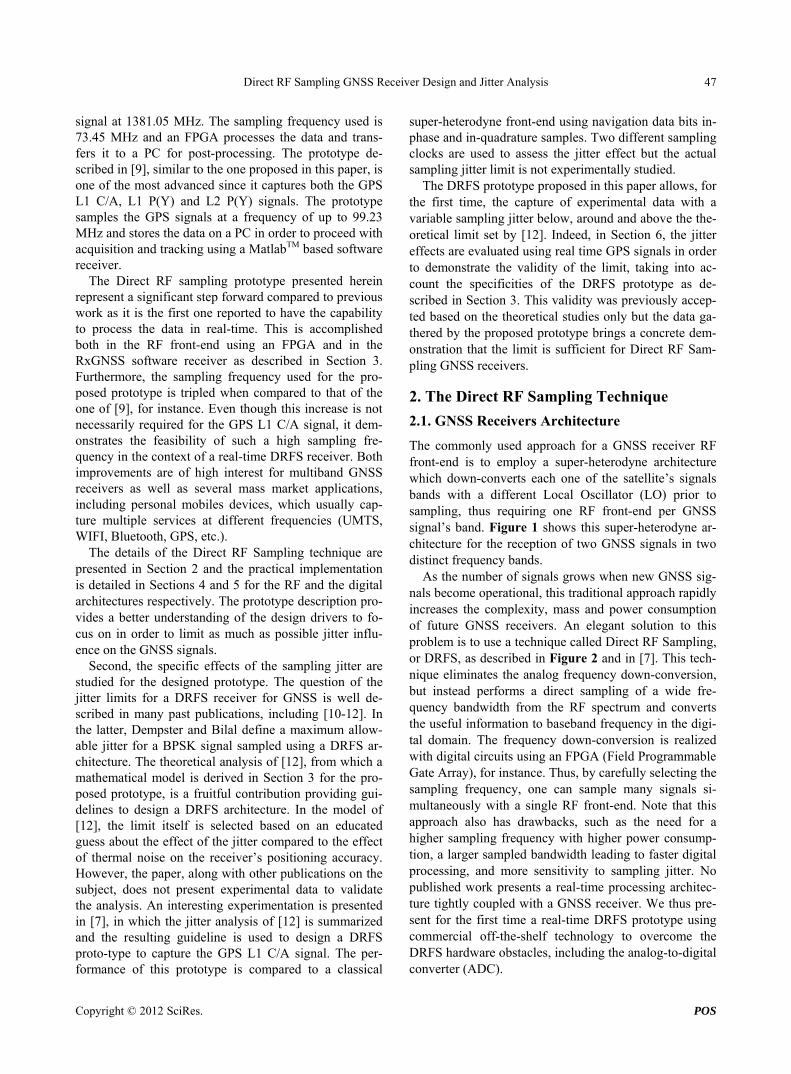
Positioning, 2012, 3, 46-61 http://dx.doi.org/10.4236/pos.2012.34007 Published Online November 2012 (http://www.SciRP.org/journal/pos)
Direct RF Sampling GNSS Receiver Design and Jitter Analysis
Guillaume Lamontagne1, René Jr. Landry2, Ammar B. Kouki2
1MDA Corporation, Satellite Systems Division, Sainte-Anne-de-Bellevue, Canada; 2École de technologie supérieure, LACIME Laboratory, Montréal, Canada. Email: [email protected], [email protected], [email protected] Received August 25th, 2012; revised September 30th, 2012; accepted October 17th 2012
ABSTRACT
This paper describes the design of a flexible Direct RF Sampling based GNSS receiver as well as its use for the verifi- cation of jitter effects on various performance metrics. The proposed architecture allows the sampling and the real-time digital signal processing of real GNSS signals. The analysis of the measurements obtained from this system validates theoretical formulations from which the sampling jitter limit is established in order not to impact the GNSS signal’s detection. Keywords: Direct RF Sampling; GNSS Receiver; Jitter
1. Introduction
Over the last decades, numerous governments invested a great deal of efforts and funds in designing, launching and operating complex Global Navigation Satellite Sys- tems (GNSS). Since the first experimental Global Posi- tioning Satellite (GPS) satellite was launched in 1978 by the United States of America (USA), many countries decided to join the race and are currently trying to gain independent access to global satellite navigation by laun- ching their own satellite constellation system. Russia was the second country to design such a system, called GLONASS, and recently enhanced its constellation with its latest launch at the end of 2011 [1]. The European Union is also developing its own constellation and cur- rently has two satellites deployed in orbit and they are going through their commissioning phase [2]. The latest to join the race is the Compass system, designed by Chi- na, which is currently ahead of the Galileo program, with eleven spacecrafts launched as of April 2012 [3].
Basically, the navigation signals transmitted by those systems follow the same trilateration positioning princi- ples as the GPS but they differ in terms of signal defini- tion (frequency, bandwidth and modulation). These dif- ferences result in GPS receivers’ design (RF front-end and digital signal processing) not being fully compatible with the other systems. On the other hand, users are looking for higher precision, better satellite visibility, greater integrity and more robustness. The combination of the various GNSS signals in a single GNSS receiver can help satisfy the users’ needs to some extent. There-
fore, the logical step is to design a universal GNSS re- ceiver that could receive and process the signals from various satellite navigation systems. However, one limi- tation in the design of a universal GNSS receiver is the RF front-end, which may be complex and/or technically limited for covering all potential GNSS bands and sig- nals. Furthermore, the sensitivity of the RF front-end is essential in several applications using high sensitivity receivers.
The objective of this paper is twofold. First, a proto- type using Direct RF Sampling (DRFS) is proposed as a first step towards a universal GNSS receiver. A wide- band RF front-end first amplifies and filters the GPS signals, which are later sampled by a high-speed ana- log-to-digital converter. The signals are then down-con- verted and filtered further in the digital domain and then sent to a custom GPS receiver. This GNSS receiver, to be referred to as the RxGNSS hereafter, performs the data demodulation required to find the Position, Velocity and Time (PVT) navigation solution. It was designed and built during previous studies at the LACIME laboratory of ÉTS as described in [4].
The first published work on DRFS that applied to the GPS dates back to 1994 [5] but the results were limited by the available sampling and processing technologies. Since then, many authors developed the concept, such as [6-9], proposing DRFS prototypes for GNSS signals along with detailed studies using post-processed data. In [6], Thor and Akos describe a DRFS prototype to capture both the GPS L1 C/A and the GPS L3 nuclear detection
Copyright © 2012 SciRes. POS
Direct RF Sampling GNSS Receiver Design and Jitter Analysis 47
signal at 1381.05 MHz. The sampling frequency used is 73.45 MHz and an FPGA processes the data and trans- fers it to a PC for post-processing. The prototype de- scribed in [9], similar to the one proposed in this paper, is one of the most advanced since it captures both the GPS L1 C/A, L1 P(Y) and L2 P(Y) signals. The prototype samples the GPS signals at a frequency of up to 99.23 MHz and stores the data on a PC in order to proceed with acquisition and tracking using a MatlabTM based software receiver.
The Direct RF sampling prototype presented herein represent a significant step forward compared to previous work as it is the first one reported to have the capability to process the data in real-time. This is accomplished both in the RF front-end using an FPGA and in the RxGNSS software receiver as described in Section 3. Furthermore, the sampling frequency used for the pro- posed prototype is tripled when compared to that of the one of [9], for instance. Even though this increase is not necessarily required for the GPS L1 C/A signal, it dem- onstrates the feasibility of such a high sampling fre- quency in the context of a real-time DRFS receiver. Both improvements are of high interest for multiband GNSS receivers as well as several mass market applications, including personal mobiles devices, which usually cap- ture multiple services at different frequencies (UMTS, WIFI, Bluetooth, GPS, etc.).
The details of the Direct RF Sampling technique are presented in Section 2 and the practical implementation is detailed in Sections 4 and 5 for the RF and the digital architectures respectively. The prototype description pro- vides a better understanding of the design drivers to fo- cus on in order to limit as much as possible jitter influ- ence on the GNSS signals.
Second, the specific effects of the sampling jitter are studied for the designed prototype. The question of the jitter limits for a DRFS receiver for GNSS is well de- scribed in many past publications, including [10-12]. In the latter, Dempster and Bilal define a maximum allow- able jitter for a BPSK signal sampled using a DRFS ar- chitecture. The theoretical analysis of [12], from which a mathematical model is derived in Section 3 for the pro- posed prototype, is a fruitful contribution providing gui- delines to design a DRFS architecture. In the model of [12], the limit itself is selected based on an educated guess about the effect of the jitter compared to the effect of thermal noise on the receiver’s positioning accuracy. However, the paper, along with other publications on the subject, does not present experimental data to validate the analysis. An interesting experimentation is presented in [7], in which the jitter analysis of [12] is summarized and the resulting guideline is used to design a DRFS proto-type to capture the GPS L1 C/A signal. The per- formance of this prototype is compared to a classical
super-heterodyne front-end using navigation data bits in- phase and in-quadrature samples. Two different sampling clocks are used to assess the jitter effect but the actual sampling jitter limit is not experimentally studied.
The DRFS prototype proposed in this paper allows, for the first time, the capture of experimental data with a variable sampling jitter below, around and above the the- oretical limit set by [12]. Indeed, in Section 6, the jitter effects are evaluated using real time GPS signals in order to demonstrate the validity of the limit, taking into ac- count the specificities of the DRFS prototype as de- scribed in Section 3. This validity was previously accep- ted based on the theoretical studies only but the data ga- thered by the proposed prototype brings a concrete dem- onstration that the limit is sufficient for Direct RF Sam- pling GNSS receivers.
2. The Direct RF Sampling Technique
2.1. GNSS Receivers Architecture
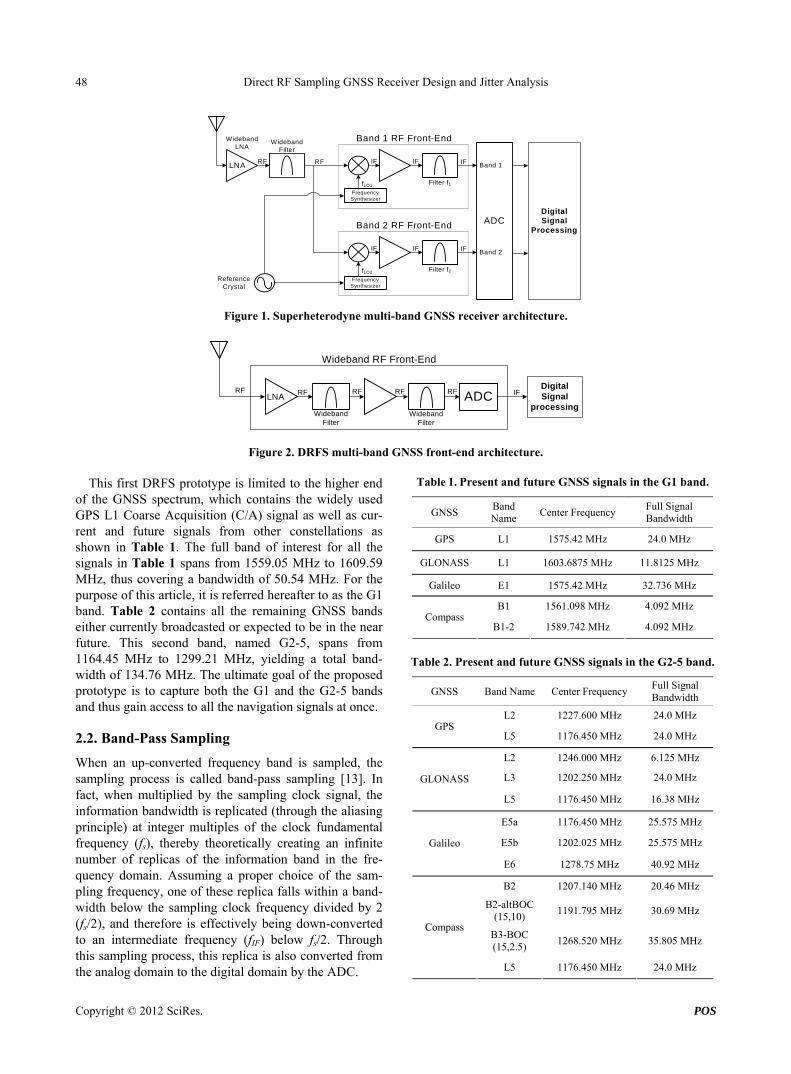
The commonly used approach for a GNSS receiver RF front-end is to employ a super-heterodyne architecture which down-converts each one of the satellite’s signals bands with a different Local Oscillator (LO) prior to sampling, thus requiring one RF front-end per GNSS signal’s band. Figure 1 shows this super-heterodyne ar- chitecture for the reception of two GNSS signals in two distinct frequency bands.
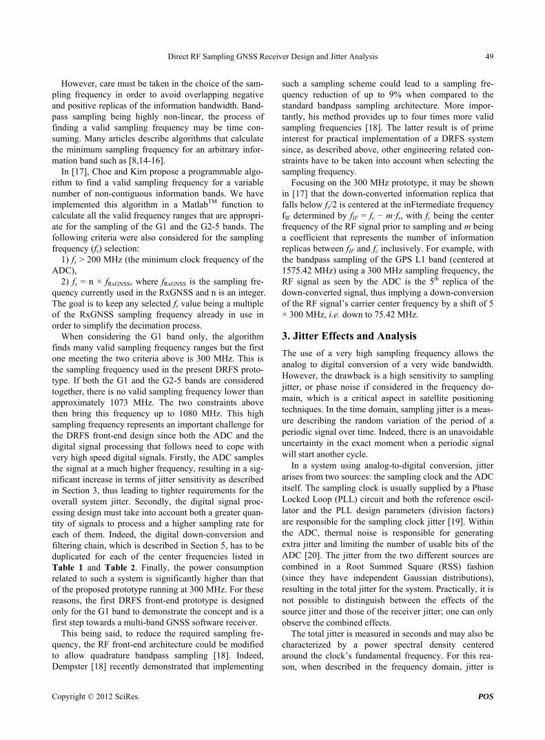
As the number of signals grows when new GNSS sig- nals become operational, this traditional approach rapidly increases the complexity, mass and power consumption of future GNSS receivers. An elegant solution to this problem is to use a technique called Direct RF Sampling, or DRFS, as described in Figure 2 and in [7]. This tech- nique eliminates the analog frequency down-conversion, but instead performs a direct sampling of a wide fre- quency bandwidth from the RF spectrum and converts the useful information to baseband frequency in the digi- tal domain. The frequency down-conversion is realized with digital circuits using an FPGA (Field Programmable Gate Array), for instance. Thus, by carefully selecting the sampling frequency, one can sample many signals si- multaneously with a single RF front-end. Note that this approach also has drawbacks, such as the need for a higher sampling frequency with higher power consump- tion, a larger sampled bandwidth leading to faster digital processing, and more sensitivity to sampling jitter. No published work presents a real-time processing architec- ture tightly coupled with a GNSS receiver. We thus pre- sent for the first time a real-time DRFS prototype using commercial off-the-shelf technology to overcome the DRFS hardware obstacles, including the analog-to-digital converter (ADC).
Copyright © 2012 SciRes. POS
Direct RF Sampling GNSS Receiver Design and Jitter Analysis
Copyright © 2012 SciRes. POS
48
Frequency Synthesizer
Digital Signal
Processing
IF IFRF RF
Band 1 RF Front-End
Reference Crystal
Filter f1
ADC
LNAIF
Frequency Synthesizer
IF IF
Band 2 RF Front-End
Filter f2
IF
Band 1
Band 2
Wideband Filter
Wideband LNA
fLO1
fLO2
Figure 1. Superheterodyne multi-band GNSS receiver architecture.
ADCRF RF
Wideband RF Front-End
Digital Signal
processingLNA
Wideband Filter
RF
Wideband Filter
RF RF IF
Figure 2. DRFS multi-band GNSS front-end architecture.
Table 1. Present and future GNSS signals in the G1 band. This first DRFS prototype is limited to the higher end of the GNSS spectrum, which contains the widely used GPS L1 Coarse Acquisition (C/A) signal as well as cur- rent and future signals from other constellations as shown in Table 1. The full band of interest for all the signals in Table 1 spans from 1559.05 MHz to 1609.59 MHz, thus covering a bandwidth of 50.54 MHz. For the purpose of this article, it is referred hereafter to as the G1 band. Table 2 contains all the remaining GNSS bands either currently broadcasted or expected to be in the near future. This second band, named G2-5, spans from 1164.45 MHz to 1299.21 MHz, yielding a total band- width of 134.76 MHz. The ultimate goal of the proposed prototype is to capture both the G1 and the G2-5 bands and thus gain access to all the navigation signals at once.
GNSS Band Name
Center Frequency Full Signal Bandwidth
GPS L1 1575.42 MHz 24.0 MHz
GLONASS L1 1603.6875 MHz 11.8125 MHz
Galileo E1 1575.42 MHz 32.736 MHz
B1 1561.098 MHz 4.092 MHz Compass
B1-2 1589.742 MHz 4.092 MHz
Table 2. Present and future GNSS signals in the G2-5 band.
GNSS Band Name Center Frequency Full Signal Bandwidth
L2 1227.600 MHz 24.0 MHz GPS
L5 1176.450 MHz 24.0 MHz
L2 1246.000 MHz 6.125 MHz
L3 1202.250 MHz 24.0 MHz GLONASS
L5 1176.450 MHz 16.38 MHz
E5a 1176.450 MHz 25.575 MHz
E5b 1202.025 MHz 25.575 MHz Galileo
E6 1278.75 MHz 40.92 MHz
B2 1207.140 MHz 20.46 MHz
B2-altBOC(15,10)
1191.795 MHz 30.69 MHz
B3-BOC (15,2.5)
1268.520 MHz 35.805 MHz Compass
L5 1176.450 MHz 24.0 MHz
2.2. Band-Pass Sampling
When an up-converted frequency band is sampled, the sampling process is called band-pass sampling [13]. In fact, when multiplied by the sampling clock signal, the information bandwidth is replicated (through the aliasing principle) at integer multiples of the clock fundamental frequency (fs), thereby theoretically creating an infinite number of replicas of the information band in the fre- quency domain. Assuming a proper choice of the sam- pling frequency, one of these replica falls within a band- width below the sampling clock frequency divided by 2 (fs/2), and therefore is effectively being down-converted to an intermediate frequency (fIF) below fs/2. Through this sampling process, this replica is also converted from the analog domain to the digital domain by the ADC.
Direct RF Sampling GNSS Receiver Design and Jitter Analysis 49
However, care must be taken in the choice of the sam- pling frequency in order to avoid overlapping negative and positive replicas of the information bandwidth. Band- pass sampling being highly non-linear, the process of finding a valid sampling frequency may be time con- suming. Many articles describe algorithms that calculate the minimum sampling frequency for an arbitrary infor- mation band such as [8,14-16].
In [17], Choe and Kim propose a programmable algo- rithm to find a valid sampling frequency for a variable number of non-contiguous information bands. We have implemented this algorithm in a MatlabTM function to calculate all the valid frequency ranges that are appropri- ate for the sampling of the G1 and the G2-5 bands. The following criteria were also considered for the sampling frequency (fs) selection:
1) fs > 200 MHz (the minimum clock frequency of the ADC),
2) fs = n × fRxGNSS, where fRxGNSS is the sampling fre- quency currently used in the RxGNSS and n is an integer. The goal is to keep any selected fs value being a multiple of the RxGNSS sampling frequency already in use in order to simplify the decimation process.
When considering the G1 band only, the algorithm finds many valid sampling frequency ranges but the first one meeting the two criteria above is 300 MHz. This is the sampling frequency used in the present DRFS proto- type. If both the G1 and the G2-5 bands are considered together, there is no valid sampling frequency lower than approximately 1073 MHz. The two constraints above then bring this frequency up to 1080 MHz. This high sampling frequency represents an important challenge for the DRFS front-end design since both the ADC and the digital signal processing that follows need to cope with very high speed digital signals. Firstly, the ADC samples the signal at a much higher frequency, resulting in a sig- nificant increase in terms of jitter sensitivity as described in Section 3, thus leading to tighter requirements for the overall system jitter. Secondly, the digital signal proc- essing design must take into account both a greater quan- tity of signals to process and a higher sampling rate for each of them. Indeed, the digital down-conversion and filtering chain, which is described in Section 5, has to be duplicated for each of the center frequencies listed in Table 1 and Table 2. Finally, the power consumption related to such a system is significantly higher than that of the proposed prototype running at 300 MHz. For these reasons, the first DRFS front-end prototype is designed only for the G1 band to demonstrate the concept and is a first step towards a multi-band GNSS software receiver.
This being said, to reduce the required sampling fre- quency, the RF front-end architecture could be modified to allow quadrature bandpass sampling [18]. Indeed, Dempster [18] recently demonstrated that implementing
such a sampling scheme could lead to a sampling fre- quency reduction of up to 9% when compared to the standard bandpass sampling architecture. More impor- tantly, his method provides up to four times more valid sampling frequencies [18]. The latter result is of prime interest for practical implementation of a DRFS system since, as described above, other engineering related con- straints have to be taken into account when selecting the sampling frequency.
Focusing on the 300 MHz prototype, it may be shown in [17] that the down-converted information replica that falls below fs/2 is centered at the inFtermediate frequency fIF determined by fIF = fc − m·fs, with fc being the center frequency of the RF signal prior to sampling and m being a coefficient that represents the number of information replicas between fIF and fc inclusively. For example, with the bandpass sampling of the GPS L1 band (centered at 1575.42 MHz) using a 300 MHz sampling frequency, the RF signal as seen by the ADC is the 5th replica of the down-converted signal, thus implying a down-conversion of the RF signal’s carrier center frequency by a shift of 5 × 300 MHz, i.e. down to 75.42 MHz.
3. Jitter Effects and Analysis
The use of a very high sampling frequency allows the analog to digital conversion of a very wide bandwidth. However, the drawback is a high sensitivity to sampling jitter, or phase noise if considered in the frequency do- main, which is a critical aspect in satellite positioning techniques. In the time domain, sampling jitter is a meas- ure describing the random variation of the period of a periodic signal over time. Indeed, there is an unavoidable uncertainty in the exact moment when a periodic signal will start another cycle.
In a system using analog-to-digital conversion, jitter arises from two sources: the sampling clock and the ADC itself. The sampling clock is usually supplied by a Phase Locked Loop (PLL) circuit and both the reference oscil- lator and the PLL design parameters (division factors) are responsible for the sampling clock jitter [19]. Within the ADC, thermal noise is responsible for generating extra jitter and limiting the number of usable bits of the ADC [20]. The jitter from the two different sources are combined in a Root Summed Square (RSS) fashion (since they have independent Gaussian distributions), resulting in the total jitter for the system. Practically, it is not possible to distinguish between the effects of the source jitter and those of the receiver jitter; one can only observe the combined effects.
The total jitter is measured in seconds and may also be characterized by a power spectral density centered around the clock’s fundamental frequency. For this rea- son, when described in the frequency domain, jitter is
Copyright © 2012 SciRes. POS
Direct RF Sampling GNSS Receiver Design and Jitter Analysis 50
commonly referred to as phase noise. Details on exact conversion from jitter to phase noise can be found in [11].
The effect of jitter on a sampled signal is the addition of noise to the sampled signal, thus reducing its Signal- to-Noise Ratio (SNR). This is particularly important in a DRFS system for GNSS signals, since the high sampled frequencies (in the L-band portion of the electro-mag- netic spectrum) render the SNR more susceptible to this jitter effect, as will be demonstrated below. The mathe- matical model itself was developed by [12] and is sum- marized here to provide a better understanding of the experimental results presented in Section 6.
For a Binary Phase Shift Keying signal, like the one generated by the GPS satellites for the GPA L1 C/A sig- nal, the noise power generated by the jitter can be calcu- lated using (1) as in [12], namely:
2 222π
πd cN A f f
2 2
(1)
where Nτ is the noise power generated by the jitter, fc is the carrier frequency of the GNSS signal at ADC input, fd is the BPSK data frequency, στ is the total system jitter and A is the constant carrier amplitude of the incoming BPSK signal at the ADC input. Equation (1) clearly shows that a higher sampling frequency will result in a higher noise power generated by the jitter.
Using the jitter as the only noise source, one can cal- culate the Signal to Jitter Ratio (SJR) of the sampled sig- nal. The total signal power (S) is considered to be the signal’s carrier power (A2/2) while the noise power is expressed by Nτ from (1), leading to the following ex- pression for the SJR:
2 2 2
1
22 2π
πd c
SSJR
Nf f
(2)
To constrain the power of the noise generated by the jitter, [12] proposes to limit the jitter noise power to 10 dB below that of the thermal noise (Nth) so that its effects can be neglected. This constraint is written as follows:
10th
SSJR
N (3)
According to [10], jitter will have more effect on the channel that conveys the GNSS data itself (as opposed, for example, to the dataless channel that conveys a pilot signal). Hence, a noise bandwidth Bd, equal to that of the GNSS signal (i.e. twice that of the GNSS data, given the double sideband spectrum), is used to calculate the ther- mal noise power (yielding kTBd [12]). Using the SJR definition of (2) and solving for στ, the jitter constraint is
expressed by:
2 22 2
2 2
80 8016π
π π
108π
d dc
d d
cd
f S ff
kTB kTB
Sf
kTB
S
(4)
where k is the Bolztmann constant (1.38 × 10⁻²³ J·K−1) and T is the noise temperature of the GNSS receiver.
The constraint given by (4) can be considered as a de- sign parameter for a GNSS DRFS receiver. As a nu- merical example, the values presented in Table 3 are used in (4) to calculate the maximum allowable jitter for the GPS L1 C/A signal. The result of this calculation is a jitter limit of 1.72 ps.
However, it is yet to be proven experimentally that the jitter limit expressed by (4) (i.e. 1.72 ps in this numerical example) actually results in the jitter having no contribu- tion to the SNR of the GNSS signal. The DRFS front-end described in this article was designed for a significantly lower total jitter in order to have a good reference in as- sessing the effects of intentionally degraded sampling jitter on the GNSS signals. A critical part of the proposed architecture is the analog-to-digital converter (ADC) and therefore a high frequency ADC from Atmel, the AT84AS004, was selected for this function because of its very low jitter (0.15 ps). The DRFS prototype was tested and analyzed in 2009 and presented in [21]. The signal’s demodulation and the data processing that follows are realized within the RxGNSS, which uses the Lyrtech VHS-ADC development board. This board, connected to a Personal Computer (PC) through a Compact PCI bus, includes a Virtex 4 FPGA from Xilinx as well as ana- log-to-digital converters and digital input/output inter- faces. The GNSS data processing implemented in the RxGNSS was developed at the LACIME laboratory in the form of a Software Defined Radio. The FPGA de- modulates 12 GPS channels in parallel with a 60 MHz clock frequency. A Microblaze microcontroller, from Xilinx, then proceeds with the acquisition and tracking of the signals in real-time using early, prompt and late cor- relators and the classical phase and delay locked loops each of which using a numerically controlled oscillator. Table 3. GPS L1 C/A parameters for maximum jitter con- straint.
Parameter Description Value
S Carrier power −158.5 dBW
T Reference noise temperature 290 K
fc Carrier nominal frequency 1575.42 MHz
fd Pseudo Random Noise (PRN) code rate 1.023 MHz
Bd Data bandwidth 100 Hz
Copyright © 2012 SciRes. POS
Direct RF Sampling GNSS Receiver Design and Jitter Analysis
Copyright © 2012 SciRes. POS
51
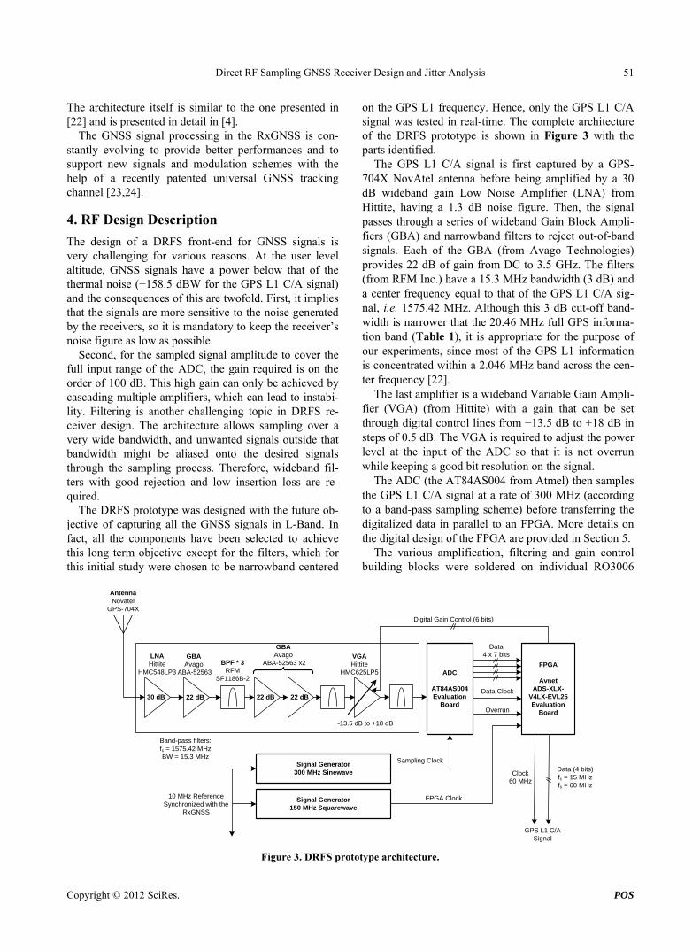
on the GPS L1 frequency. Hence, only the GPS L1 C/A signal was tested in real-time. The complete architecture of the DRFS prototype is shown in Figure 3 with the parts identified.
The architecture itself is similar to the one presented in [22] and is presented in detail in [4].
The GNSS signal processing in the RxGNSS is con- stantly evolving to provide better performances and to support new signals and modulation schemes with the help of a recently patented universal GNSS tracking channel [23,24].
The GPS L1 C/A signal is first captured by a GPS- 704X NovAtel antenna before being amplified by a 30 dB wideband gain Low Noise Amplifier (LNA) from Hittite, having a 1.3 dB noise figure. Then, the signal passes through a series of wideband Gain Block Ampli- fiers (GBA) and narrowband filters to reject out-of-band signals. Each of the GBA (from Avago Technologies) provides 22 dB of gain from DC to 3.5 GHz. The filters (from RFM Inc.) have a 15.3 MHz bandwidth (3 dB) and a center frequency equal to that of the GPS L1 C/A sig- nal, i.e. 1575.42 MHz. Although this 3 dB cut-off band- width is narrower that the 20.46 MHz full GPS informa- tion band (Table 1), it is appropriate for the purpose of our experiments, since most of the GPS L1 information is concentrated within a 2.046 MHz band across the cen- ter frequency [22].
4. RF Design Description
The design of a DRFS front-end for GNSS signals is very challenging for various reasons. At the user level altitude, GNSS signals have a power below that of the thermal noise (−158.5 dBW for the GPS L1 C/A signal) and the consequences of this are twofold. First, it implies that the signals are more sensitive to the noise generated by the receivers, so it is mandatory to keep the receiver’s noise figure as low as possible.
Second, for the sampled signal amplitude to cover the full input range of the ADC, the gain required is on the order of 100 dB. This high gain can only be achieved by cascading multiple amplifiers, which can lead to instabi- lity. Filtering is another challenging topic in DRFS re- ceiver design. The architecture allows sampling over a very wide bandwidth, and unwanted signals outside that bandwidth might be aliased onto the desired signals through the sampling process. Therefore, wideband fil- ters with good rejection and low insertion loss are re- quired.
The last amplifier is a wideband Variable Gain Ampli- fier (VGA) (from Hittite) with a gain that can be set through digital control lines from −13.5 dB to +18 dB in steps of 0.5 dB. The VGA is required to adjust the power level at the input of the ADC so that it is not overrun while keeping a good bit resolution on the signal.
The ADC (the AT84AS004 from Atmel) then samples the GPS L1 C/A signal at a rate of 300 MHz (according to a band-pass sampling scheme) before transferring the digitalized data in parallel to an FPGA. More details on the digital design of the FPGA are provided in Section 5.
The DRFS prototype was designed with the future ob- jective of capturing all the GNSS signals in L-Band. In fact, all the components have been selected to achieve this long term objective except for the filters, which for this initial study were chosen to be narrowband centered
The various amplification, filtering and gain control building blocks were soldered on individual RO3006
LNAHittite
HMC548LP3 ADC
AT84AS004 Evaluation
Board
Signal Generator300 MHz Sinewave
FPGA
AvnetADS-XLX-
V4LX-EVL25Evaluation
Board
Antenna Novatel
GPS-704X
GBAAvago
ABA-52563
10 MHz ReferenceSynchronized with the
RxGNSS
Data4 x 7 bits
Digital Gain Control (6 bits)
GPS L1 C/A Signal
Sampling Clock
30 dB
VGAHittite
HMC625LP5
-13.5 dB to +18 dB
22 dB 22 dB 22 dBData Clock
Overrun
Data (4 bits)fc = 15 MHzfs = 60 MHz
Clock60 MHz
GBAAvago
ABA-52563 x2BPF * 3RFM
SF1186B-2
Band-pass filters: fc = 1575.42 MHzBW = 15.3 MHz
Signal Generator150 MHz Squarewave
FPGA Clock
Figure 3. DRFS prototype architecture.
Direct RF Sampling GNSS Receiver Design and Jitter Analysis 52
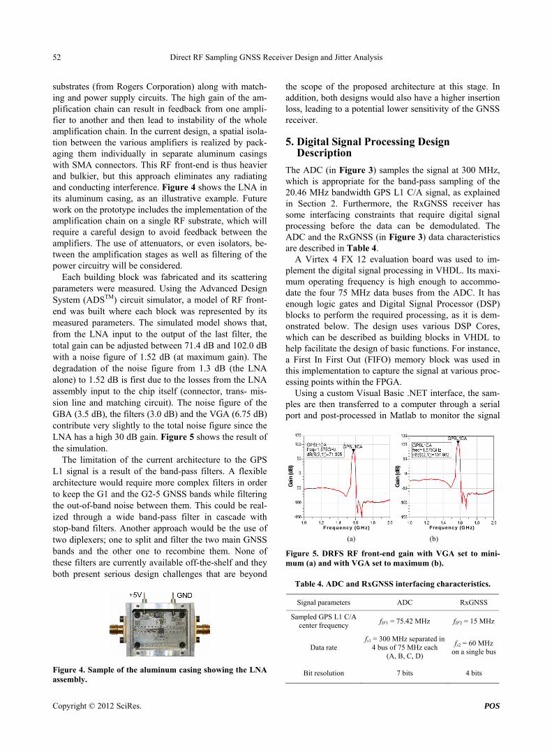
substrates (from Rogers Corporation) along with match- ing and power supply circuits. The high gain of the am- plification chain can result in feedback from one ampli-fier to another and then lead to instability of the whole amplification chain. In the current design, a spatial isola- tion between the various amplifiers is realized by pack- aging them individually in separate aluminum casings with SMA connectors. This RF front-end is thus heavier and bulkier, but this approach eliminates any radiating and conducting interference. Figure 4 shows the LNA in its aluminum casing, as an illustrative example. Future work on the prototype includes the implementation of the amplification chain on a single RF substrate, which will require a careful design to avoid feedback between the amplifiers. The use of attenuators, or even isolators, be- tween the amplification stages as well as filtering of the power circuitry will be considered.
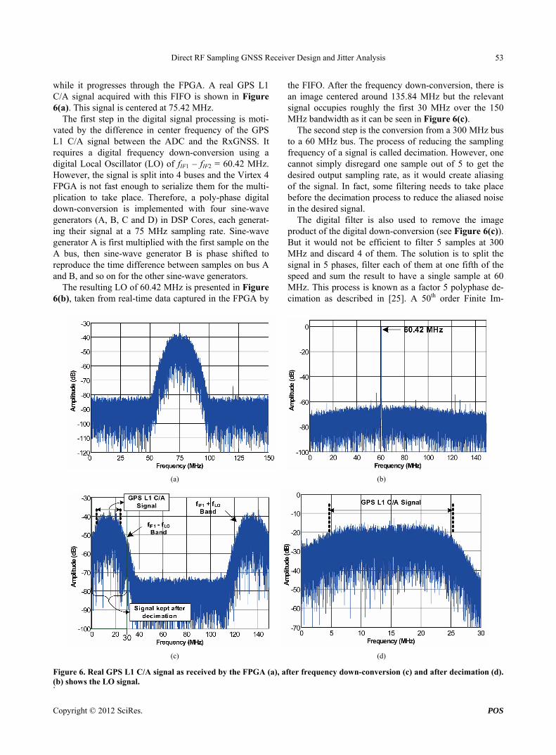
Each building block was fabricated and its scattering parameters were measured. Using the Advanced Design System (ADSTM) circuit simulator, a model of RF front- end was built where each block was represented by its measured parameters. The simulated model shows that, from the LNA input to the output of the last filter, the total gain can be adjusted between 71.4 dB and 102.0 dB with a noise figure of 1.52 dB (at maximum gain). The degradation of the noise figure from 1.3 dB (the LNA alone) to 1.52 dB is first due to the losses from the LNA assembly input to the chip itself (connector, trans- mis-sion line and matching circuit). The noise figure of the GBA (3.5 dB), the filters (3.0 dB) and the VGA (6.75 dB) contribute very slightly to the total noise figure since the LNA has a high 30 dB gain. Figure 5 shows the result of the simulation.
The limitation of the current architecture to the GPS L1 signal is a result of the band-pass filters. A flexible architecture would require more complex filters in order to keep the G1 and the G2-5 GNSS bands while filtering the out-of-band noise between them. This could be real- ized through a wide band-pass filter in cascade with stop-band filters. Another approach would be the use of two diplexers; one to split and filter the two main GNSS bands and the other one to recombine them. None of these filters are currently available off-the-shelf and they both present serious design challenges that are beyond
Figure 4. Sample of the aluminum casing showing the LNA assembly.
the scope of the proposed architecture at this stage. In addition, both designs would also have a higher insertion loss, leading to a potential lower sensitivity of the GNSS receiver.
5. Digital Signal Processing Design Description
The ADC (in Figure 3) samples the signal at 300 MHz, which is appropriate for the band-pass sampling of the 20.46 MHz bandwidth GPS L1 C/A signal, as explained in Section 2. Furthermore, the RxGNSS receiver has some interfacing constraints that require digital signal processing before the data can be demodulated. The ADC and the RxGNSS (in Figure 3) data characteristics are described in Table 4.
A Virtex 4 FX 12 evaluation board was used to im- plement the digital signal processing in VHDL. Its maxi- mum operating frequency is high enough to accommo- date the four 75 MHz data buses from the ADC. It has enough logic gates and Digital Signal Processor (DSP) blocks to perform the required processing, as it is dem- onstrated below. The design uses various DSP Cores, which can be described as building blocks in VHDL to help facilitate the design of basic functions. For instance, a First In First Out (FIFO) memory block was used in this implementation to capture the signal at various proc- essing points within the FPGA.
Using a custom Visual Basic .NET interface, the sam- ples are then transferred to a computer through a serial port and post-processed in Matlab to monitor the signal
Frequency (G H z)
Gai
n (d
B)
F requency (G Hz)
Gai
n (d
B)
(a) (b)
Figure 5. DRFS RF front-end gain with VGA set to mini- mum (a) and with VGA set to maximum (b).
Table 4. ADC and RxGNSS interfacing characteristics.
Signal parameters ADC RxGNSS
Sampled GPS L1 C/A center frequency
fIF1 = 75.42 MHz fIF2 = 15 MHz
Data rate fs1 = 300 MHz separated in
4 bus of 75 MHz each (A, B, C, D)
fs2 = 60 MHz on a single bus
Bit resolution 7 bits 4 bits
Copyright © 2012 SciRes. POS
Direct RF Sampling GNSS Receiver Design and Jitter Analysis 53
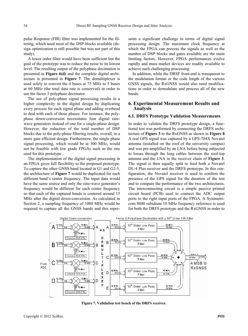
while it progresses through the FPGA. A real GPS L1 C/A signal acquired with this FIFO is shown in Figure 6(a). This signal is centered at 75.42 MHz.
The first step in the digital signal processing is moti- vated by the difference in center frequency of the GPS L1 C/A signal between the ADC and the RxGNSS. It requires a digital frequency down-conversion using a digital Local Oscillator (LO) of fIF1 – fIF2 = 60.42 MHz. However, the signal is split into 4 buses and the Virtex 4 FPGA is not fast enough to serialize them for the multi- plication to take place. Therefore, a poly-phase digital down-conversion is implemented with four sine-wave generators (A, B, C and D) in DSP Cores, each generat- ing their signal at a 75 MHz sampling rate. Sine-wave generator A is first multiplied with the first sample on the A bus, then sine-wave generator B is phase shifted to reproduce the time difference between samples on bus A and B, and so on for the other sine-wave generators.
The resulting LO of 60.42 MHz is presented in Figure 6(b), taken from real-time data captured in the FPGA by
the FIFO. After the frequency down-conversion, there is an image centered around 135.84 MHz but the relevant signal occupies roughly the first 30 MHz over the 150 MHz bandwidth as it can be seen in Figure 6(c).
The second step is the conversion from a 300 MHz bus to a 60 MHz bus. The process of reducing the sampling frequency of a signal is called decimation. However, one cannot simply disregard one sample out of 5 to get the desired output sampling rate, as it would create aliasing of the signal. In fact, some filtering needs to take place before the decimation process to reduce the aliased noise in the desired signal.
The digital filter is also used to remove the image product of the digital down-conversion (see Figure 6(c)). But it would not be efficient to filter 5 samples at 300 MHz and discard 4 of them. The solution is to split the signal in 5 phases, filter each of them at one fifth of the speed and sum the result to have a single sample at 60 MHz. This process is known as a factor 5 polyphase de- cimation as described in [25]. A 50th order Finite Im-
(a) (b)
(c) (d)
Figure 6. Real GPS L1 C/A signal as received by the FPGA (a), after frequency down-conversion (c) and after decimation (d). ) shows the LO signal. (b .
Copyright © 2012 SciRes. POS
Direct RF Sampling GNSS Receiver Design and Jitter Analysis 54
pulse Response (FIR) filter was implemented for the fil- tering, which used most of the DSP blocks available (de- sign optimization is still possible but was not part of this study).
A lower order filter would have been sufficient but the goal of the prototype was to reduce the noise to its lowest level. The resulting output of the polyphase decimation is presented in Figure 6(d) and the complete digital archi- tecture is presented in Figure 7. The demultiplexer is used solely to convert the 4 buses at 75 MHz to 5 buses at 60 MHz (the total data rate is conserved) in order to use the factor 5 polyphase decimator.
The use of poly-phase signal processing results in a higher complexity in the digital design by duplicating every process for each signal phase and adding overhead to deal with each of those phases. For instance, the poly- phase down-conversion necessitates four digital sine- wave generators instead of one for a single-phase design. However, the reduction of the total number of DSP blocks due to the poly-phase filtering results, overall, in a more gate efficient design. Furthermore, the single phase signal processing, which would be at 300 MHz, would not be feasible with low grade FPGAs such as the one used for this prototype.
The implementation of the digital signal processing in an FPGA gives full flexibility to the proposed prototype. To capture the other GNSS band located in G1 and G2-5, the architecture of Figure 7 would be duplicated for each different band’s center frequency. The input data would have the same source and only the sine-wave generator’s frequency would be different for each center frequency so that each of the captured bands is centered around 15 MHz after the digital down-conversion. As calculated in Section 2, a sampling frequency of 1080 MHz would be required to capture all the GNSS bands and this repre-
sents a significant challenge in terms of digital signal processing design. The maximum clock frequency at which the FPGA can process the signals as well as the number of DSP blocks and gates available are the main limiting factors. However, FPGA performances evolve rapidly and mass market devices are readily available to achieve such challenging processing.
In addition, while the DRSF front-end is transparent to the modulation format or the code length of the various GNSS signals, the RxGNSS would also need modifica- tions in order to demodulate and process all of the new bands.
6. Experimental Measurement Results and Analysis
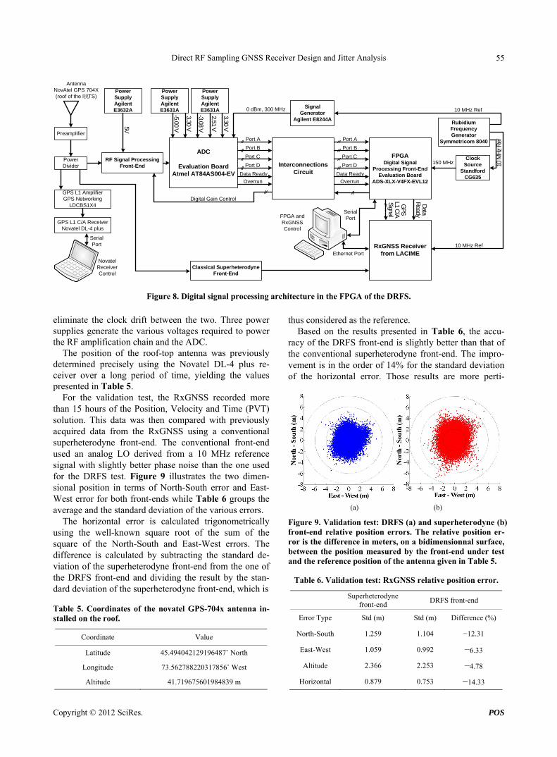
6.1. DRFS Prototype Validation Measurements
In order to validate the DRFS prototype design, a func- tional test was performed by connecting the DRFS archi- tecture of Figure 3 to the RxGNSS as shown in Figure 8. A real GPS signal was captured by a GPS-704X Novatel antenna (installed on the roof of the university campus) and was pre-amplified by an LNA before being subjected to losses through the long cables between the roof-top antenna and the LNA in the receiver chain of Figure 3. The signal is then equally split to feed both a Novatel DL-4 Plus receiver and the DRFS prototype. In this con- figuration, the Novatel receiver is used to confirm the presence of the GPS signal for the duration of the test and to compare the performance of the two architectures. The interconnecting circuit is a simple passive printed circuit board (PCB) used to connect the ADC output ports to the right input ports of the FPGA. A Symmetri- com 8040 rubidium 10 MHz frequency reference is used for both the DRFS prototype and the RxGNSS in order to
Figure 7. Validation test bench of the DRFS receiver.
Copyright © 2012 SciRes. POS
Direct RF Sampling GNSS Receiver Design and Jitter Analysis 55
Power SupplyAgilent E3632A
Power SupplyAgilent E3631A
Power SupplyAgilent E3631A
Signal Generator
Agilent E8244A
Clock Source
Standford CG635
GPS L1 C/A ReceiverNovatel DL-4 plus
RxGNSS Receiver from LACIME
RF Signal Processing Front-End
ADC
Evaluation BoardAtmel AT84AS004-EV
FPGA and RxGNSS Control
5V
Serial Port
Novatel Receiver Control
Antenna NovAtel GPS 704X(roof of the l捝TS)
3.30 V
3.30 V
0 dBm, 300 MHz
Interconnections Circuit
Port A
Port B
Port C
Port D
Data Ready
Overrun
Digital Gain Control GPS
L1 C/A
S
ignal
Data
Ready
Ethernet Port
-5.00 V
-3.08 V
2.51 V
150 MHz
Rubidium Frequency Generator
Symmetricom 8040
10 MHz Ref
10 MHz Ref
10 M
Hz
Ref
Serial Port
Preamplifier
GPS L1 AmplifierGPS Networking
LDCBS1X4
Power Divider
Classical Superheterodyne Front-End
FPGA Digital Signal
Processing Front-EndEvaluation Board
ADS-XLX-V4FX-EVL12
Port A
Port B
Port C
Port D
Data Ready
Overrun
Figure 8. Digital signal processing architecture in the FPGA of the DRFS. eliminate the clock drift between the two. Three power supplies generate the various voltages required to power the RF amplification chain and the ADC.
The position of the roof-top antenna was previously determined precisely using the Novatel DL-4 plus re- ceiver over a long period of time, yielding the values presented in Table 5.
For the validation test, the RxGNSS recorded more than 15 hours of the Position, Velocity and Time (PVT) solution. This data was then compared with previously acquired data from the RxGNSS using a conventional superheterodyne front-end. The conventional front-end used an analog LO derived from a 10 MHz reference signal with slightly better phase noise than the one used for the DRFS test. Figure 9 illustrates the two dimen- sional position in terms of North-South error and East- West error for both front-ends while Table 6 groups the average and the standard deviation of the various errors.
The horizontal error is calculated trigonometrically using the well-known square root of the sum of the square of the North-South and East-West errors. The difference is calculated by subtracting the standard de- viation of the superheterodyne front-end from the one of the DRFS front-end and dividing the result by the stan- dard deviation of the superheterodyne front-end, which is Table 5. Coordinates of the novatel GPS-704x antenna in-stalled on the roof.
Coordinate Value
Latitude 45.494042129196487˚ North
Longitude 73.562788220317856˚ West
Altitude 41.719675601984839 m
thus considered as the reference. Based on the results presented in Table 6, the accu-
racy of the DRFS front-end is slightly better than that of the conventional superheterodyne front-end. The impro- vement is in the order of 14% for the standard deviation of the horizontal error. Those results are more perti-
(a) (b)
(a) (b)
Figure 9. Validation test: DRFS (a) and superheterodyne (b) front-end relative position errors. The relative position er- ror is the difference in meters, on a bidimensionnal surface, between the position measured by the front-end under test and the reference position of the antenna given in Table 5.
Table 6. Validation test: RxGNSS relative position error.
Superheterodyne
front-end DRFS front-end
Error Type Std (m) Std (m) Difference (%)
North-South 1.259 1.104 −12.31
East-West 1.059 0.992 −6.33
Altitude 2.366 2.253 −4.78
Horizontal 0.879 0.753 −14.33
Copyright © 2012 SciRes. POS
Direct RF Sampling GNSS Receiver Design and Jitter Analysis 56
ment in the context of measuring a trend in relative terms, rather than absolute terms, considering the fact that the two front-ends are difficult to compare because of their significantly different architecture. Nevertheless, our va- lidation test demonstrated that a DRFS front-end can provide similar position accuracy when compared to a conventional superheterodyne front-end.
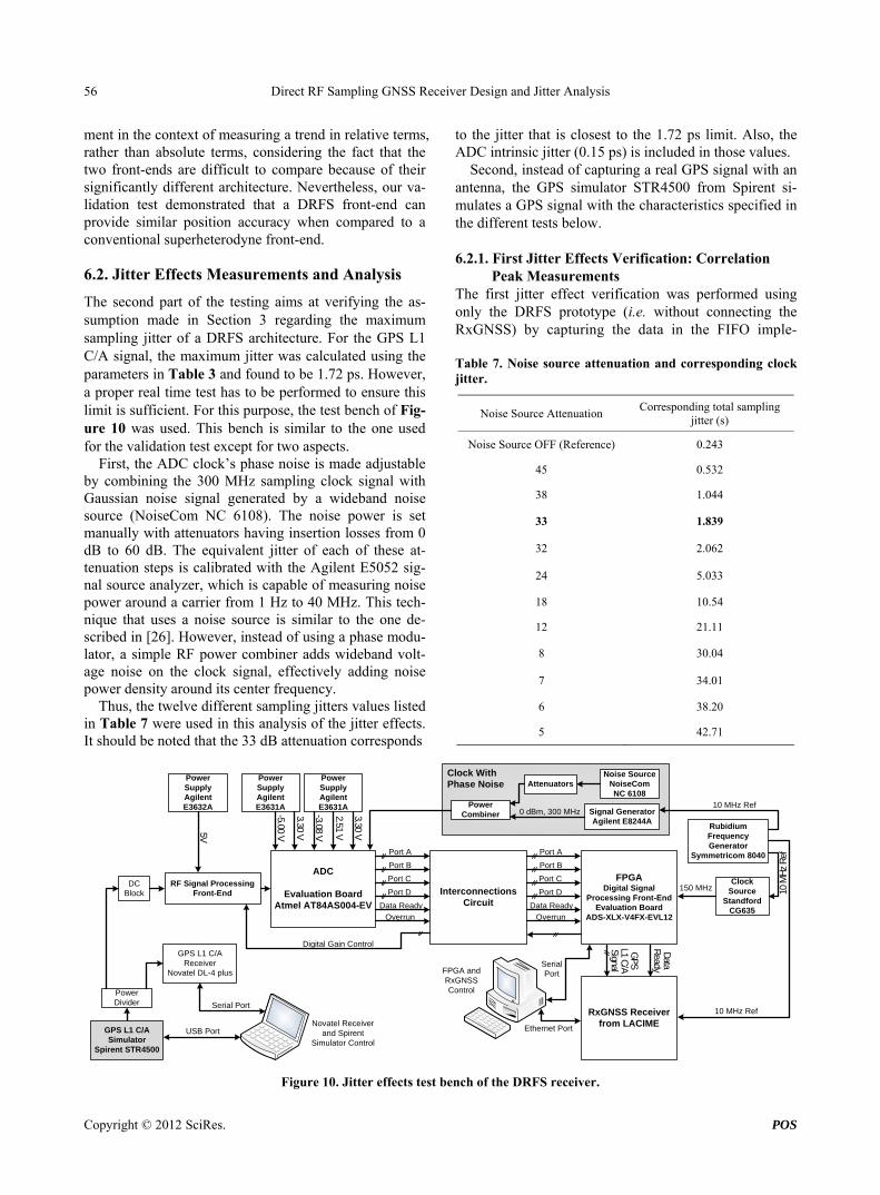
6.2. Jitter Effects Measurements and Analysis
The second part of the testing aims at verifying the as- sumption made in Section 3 regarding the maximum sampling jitter of a DRFS architecture. For the GPS L1 C/A signal, the maximum jitter was calculated using the parameters in Table 3 and found to be 1.72 ps. However, a proper real time test has to be performed to ensure this limit is sufficient. For this purpose, the test bench of Fig- ure 10 was used. This bench is similar to the one used for the validation test except for two aspects.
First, the ADC clock’s phase noise is made adjustable by combining the 300 MHz sampling clock signal with Gaussian noise signal generated by a wideband noise source (NoiseCom NC 6108). The noise power is set manually with attenuators having insertion losses from 0 dB to 60 dB. The equivalent jitter of each of these at- tenuation steps is calibrated with the Agilent E5052 sig- nal source analyzer, which is capable of measuring noise power around a carrier from 1 Hz to 40 MHz. This tech- nique that uses a noise source is similar to the one de- scribed in [26]. However, instead of using a phase modu- lator, a simple RF power combiner adds wideband volt- age noise on the clock signal, effectively adding noise power density around its center frequency.
Thus, the twelve different sampling jitters values listed in Table 7 were used in this analysis of the jitter effects. It should be noted that the 33 dB attenuation corresponds
to the jitter that is closest to the 1.72 ps limit. Also, the ADC intrinsic jitter (0.15 ps) is included in those values.
Second, instead of capturing a real GPS signal with an antenna, the GPS simulator STR4500 from Spirent si- mulates a GPS signal with the characteristics specified in the different tests below.
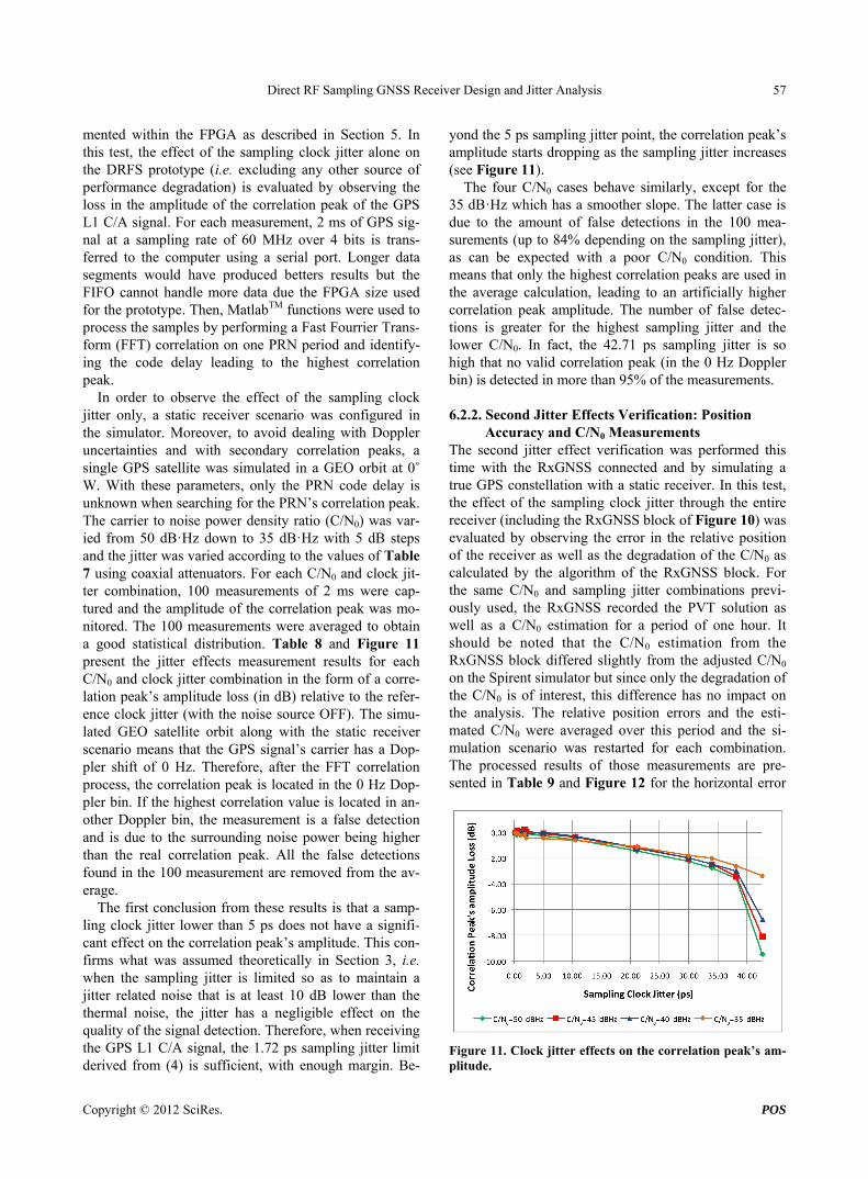
6.2.1. First Jitter Effects Verification: Correlation Peak Measurements
The first jitter effect verification was performed using only the DRFS prototype (i.e. without connecting the RxGNSS) by capturing the data in the FIFO imple- Table 7. Noise source attenuation and corresponding clock jitter.
Noise Source Attenuation Corresponding total sampling
jitter (s)
Noise Source OFF (Reference) 0.243
45 0.532
38 1.044
33 1.839
32 2.062
24 5.033
18 10.54
12 21.11
8 30.04
7 34.01
6 38.20
5 42.71
Power SupplyAgilent E3632A
Power SupplyAgilent E3631A
Power SupplyAgilent E3631A
Clock Source
Standford CG635
GPS L1 C/A Receiver
Novatel DL-4 plus
RxGNSS Receiver from LACIME
RF Signal Processing Front-End
ADC
Evaluation BoardAtmel AT84AS004-EV
FPGA and RxGNSS Control
5V
Serial Port
3.30 V
3.30 V
Interconnections Circuit
Port A
Port B
Port C
Port D
Data Ready
Overrun
Digital Gain Control GPS
L1 C/A
Signal
Data
Ready
Ethernet Port
-5.00 V
-3.08 V
2.51 V
150 MHz
10 MHz Ref
10 MHz Ref
10 M
Hz
Ref
Serial Port
Power Divider
FPGA Digital Signal
Processing Front-EndEvaluation Board
ADS-XLX-V4FX-EVL12
Port A
Port B
Port C
Port D
Data Ready
Overrun
Signal GeneratorAgilent E8244A
0 dBm, 300 MHzPower
Combiner
Noise SourceNoiseCom NC 6108
AttenuatorsClock With Phase Noise
Rubidium Frequency Generator
Symmetricom 8040
USB PortGPS L1 C/A Simulator
Spirent STR4500
DC Block
Novatel Receiver and Spirent
Simulator Control
Figure 10. Jitter effects test bench of the DRFS receiver.
Copyright © 2012 SciRes. POS
Direct RF Sampling GNSS Receiver Design and Jitter Analysis 57
mented within the FPGA as described in Section 5. In this test, the effect of the sampling clock jitter alone on the DRFS prototype (i.e. excluding any other source of performance degradation) is evaluated by observing the loss in the amplitude of the correlation peak of the GPS L1 C/A signal. For each measurement, 2 ms of GPS sig- nal at a sampling rate of 60 MHz over 4 bits is trans- ferred to the computer using a serial port. Longer data segments would have produced betters results but the FIFO cannot handle more data due the FPGA size used for the prototype. Then, MatlabTM functions were used to process the samples by performing a Fast Fourrier Trans- form (FFT) correlation on one PRN period and identify-ing the code delay leading to the highest correlation peak.
In order to observe the effect of the sampling clock jitter only, a static receiver scenario was configured in the simulator. Moreover, to avoid dealing with Doppler uncertainties and with secondary correlation peaks, a single GPS satellite was simulated in a GEO orbit at 0˚ W. With these parameters, only the PRN code delay is unknown when searching for the PRN’s correlation peak. The carrier to noise power density ratio (C/N0) was var- ied from 50 dB·Hz down to 35 dB·Hz with 5 dB steps and the jitter was varied according to the values of Table 7 using coaxial attenuators. For each C/N0 and clock jit- ter combination, 100 measurements of 2 ms were cap- tured and the amplitude of the correlation peak was mo- nitored. The 100 measurements were averaged to obtain a good statistical distribution. Table 8 and Figure 11 present the jitter effects measurement results for each C/N0 and clock jitter combination in the form of a corre- lation peak’s amplitude loss (in dB) relative to the refer- ence clock jitter (with the noise source OFF). The simu- lated GEO satellite orbit along with the static receiver scenario means that the GPS signal’s carrier has a Dop- pler shift of 0 Hz. Therefore, after the FFT correlation process, the correlation peak is located in the 0 Hz Dop- pler bin. If the highest correlation value is located in an- other Doppler bin, the measurement is a false detection and is due to the surrounding noise power being higher than the real correlation peak. All the false detections found in the 100 measurement are removed from the av- erage.
The first conclusion from these results is that a samp- ling clock jitter lower than 5 ps does not have a signifi- cant effect on the correlation peak’s amplitude. This con- firms what was assumed theoretically in Section 3, i.e. when the sampling jitter is limited so as to maintain a jitter related noise that is at least 10 dB lower than the thermal noise, the jitter has a negligible effect on the quality of the signal detection. Therefore, when receiving the GPS L1 C/A signal, the 1.72 ps sampling jitter limit derived from (4) is sufficient, with enough margin. Be-
yond the 5 ps sampling jitter point, the correlation peak’s amplitude starts dropping as the sampling jitter increases (see Figure 11).
The four C/N0 cases behave similarly, except for the 35 dB·Hz which has a smoother slope. The latter case is due to the amount of false detections in the 100 mea- surements (up to 84% depending on the sampling jitter), as can be expected with a poor C/N0 condition. This means that only the highest correlation peaks are used in the average calculation, leading to an artificially higher correlation peak amplitude. The number of false detec- tions is greater for the highest sampling jitter and the lower C/N0. In fact, the 42.71 ps sampling jitter is so high that no valid correlation peak (in the 0 Hz Doppler bin) is detected in more than 95% of the measurements.
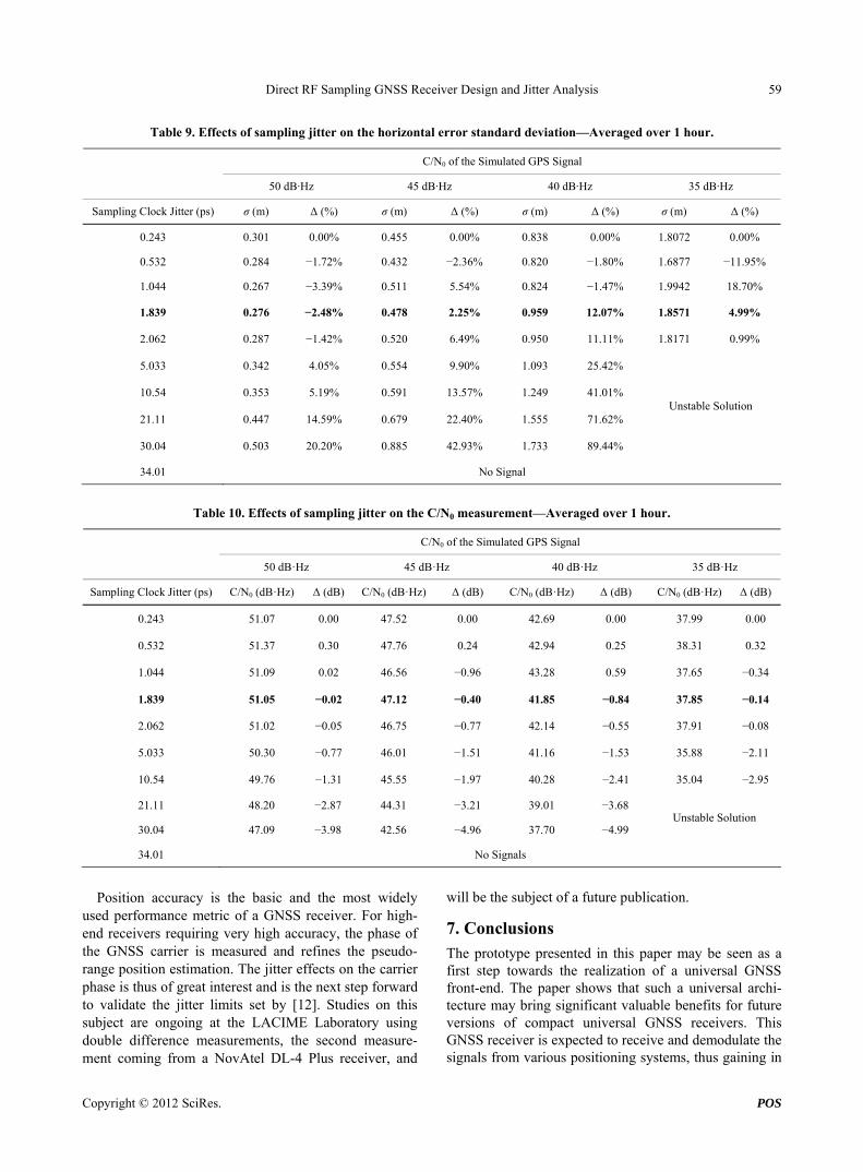
6.2.2. Second Jitter Effects Verification: Position Accuracy and C/N0 Measurements
The second jitter effect verification was performed this time with the RxGNSS connected and by simulating a true GPS constellation with a static receiver. In this test, the effect of the sampling clock jitter through the entire receiver (including the RxGNSS block of Figure 10) was evaluated by observing the error in the relative position of the receiver as well as the degradation of the C/N0 as calculated by the algorithm of the RxGNSS block. For the same C/N0 and sampling jitter combinations previ- ously used, the RxGNSS recorded the PVT solution as well as a C/N0 estimation for a period of one hour. It should be noted that the C/N0 estimation from the RxGNSS block differed slightly from the adjusted C/N0 on the Spirent simulator but since only the degradation of the C/N0 is of interest, this difference has no impact on the analysis. The relative position errors and the esti- mated C/N0 were averaged over this period and the si-mulation scenario was restarted for each combination. The processed results of those measurements are pre- sented in Table 9 and Figure 12 for the horizontal error
Figure 11. Clock jitter effects on the correlation peak’s am- litude. p
Copyright © 2012 SciRes. POS
Direct RF Sampling GNSS Receiver Design and Jitter Analysis 58
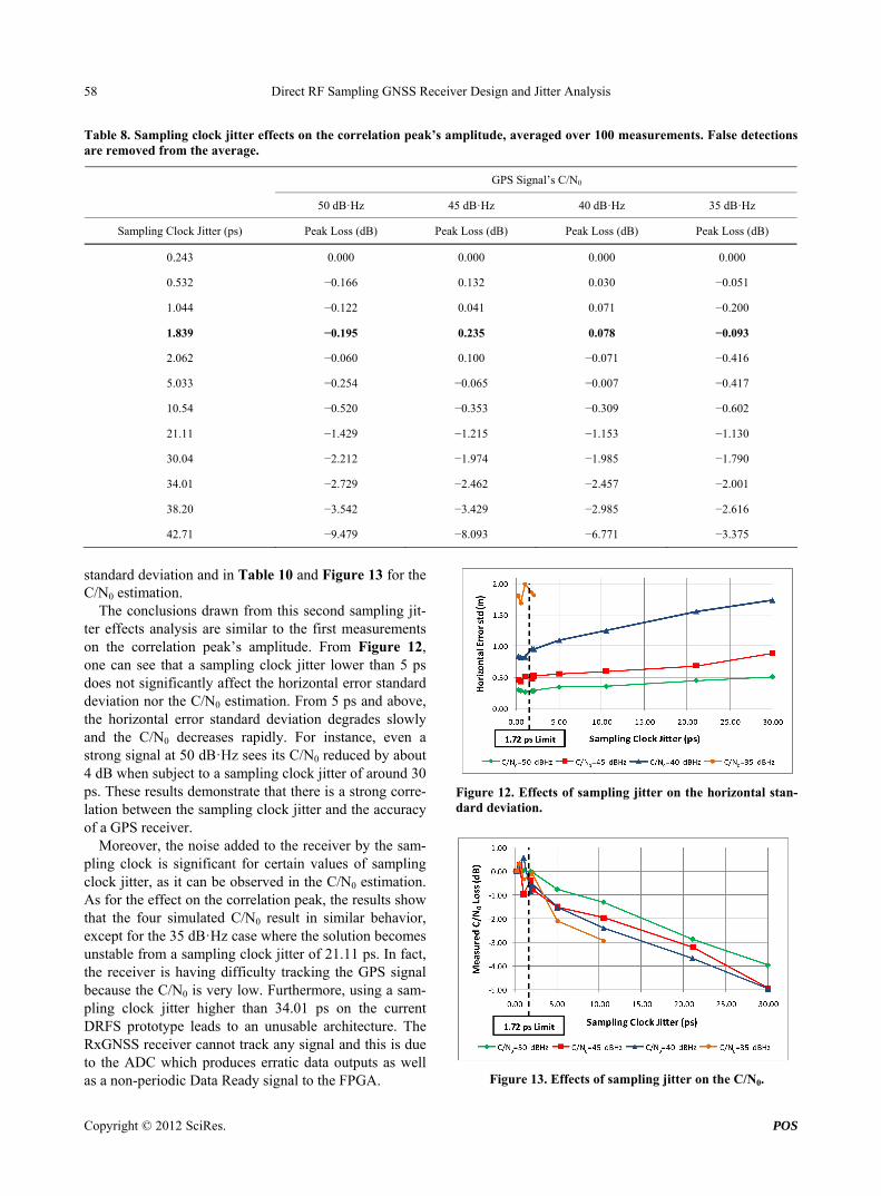
Table 8. Sampling clock jitter effects on the correlation peak’s amplitude, averaged over 100 measurements. False detections are removed from the average.
GPS Signal’s C/N0
50 dB·Hz 45 dB·Hz 40 dB·Hz 35 dB·Hz
Sampling Clock Jitter (ps) Peak Loss (dB) Peak Loss (dB) Peak Loss (dB) Peak Loss (dB)
0.243 0.000 0.000 0.000 0.000
0.532 −0.166 0.132 0.030 −0.051
1.044 −0.122 0.041 0.071 −0.200
1.839 −0.195 0.235 0.078 −0.093
2.062 −0.060 0.100 −0.071 −0.416
5.033 −0.254 −0.065 −0.007 −0.417
10.54 −0.520 −0.353 −0.309 −0.602
21.11 −1.429 −1.215 −1.153 −1.130
30.04 −2.212 −1.974 −1.985 −1.790
34.01 −2.729 −2.462 −2.457 −2.001
38.20 −3.542 −3.429 −2.985 −2.616
42.71 −9.479 −8.093 −6.771 −3.375
standard deviation and in Table 10 and Figure 13 for the C/N0 estimation.
The conclusions drawn from this second sampling jit- ter effects analysis are similar to the first measurements on the correlation peak’s amplitude. From Figure 12, one can see that a sampling clock jitter lower than 5 ps does not significantly affect the horizontal error standard deviation nor the C/N0 estimation. From 5 ps and above, the horizontal error standard deviation degrades slowly and the C/N0 decreases rapidly. For instance, even a strong signal at 50 dB·Hz sees its C/N0 reduced by about 4 dB when subject to a sampling clock jitter of around 30 ps. These results demonstrate that there is a strong corre- lation between the sampling clock jitter and the accuracy of a GPS receiver.
Moreover, the noise added to the receiver by the sam- pling clock is significant for certain values of sampling clock jitter, as it can be observed in the C/N0 estimation. As for the effect on the correlation peak, the results show that the four simulated C/N0 result in similar behavior, except for the 35 dB·Hz case where the solution becomes unstable from a sampling clock jitter of 21.11 ps. In fact, the receiver is having difficulty tracking the GPS signal because the C/N0 is very low. Furthermore, using a sam- pling clock jitter higher than 34.01 ps on the current DRFS prototype leads to an unusable architecture. The RxGNSS receiver cannot track any signal and this is due to the ADC which produces erratic data outputs as well as a non-periodic Data Ready signal to the FPGA.
Figure 12. Effects of sampling jitter on the horizontal stan-dard deviation.
Figure 13. Effects of sampling jitter on the C/N0.
Copyright © 2012 SciRes. POS
Direct RF Sampling GNSS Receiver Design and Jitter Analysis 59
Table 9. Effects of sampling jitter on the horizontal error standard deviation—Averaged over 1 hour.
C/N0 of the Simulated GPS Signal
50 dB·Hz 45 dB·Hz 40 dB·Hz 35 dB·Hz
Sampling Clock Jitter (ps) σ (m) Δ (%) σ (m) Δ (%) σ (m) Δ (%) σ (m) Δ (%)
0.243 0.301 0.00% 0.455 0.00% 0.838 0.00% 1.8072 0.00%
0.532 0.284 −1.72% 0.432 −2.36% 0.820 −1.80% 1.6877 −11.95%
1.044 0.267 −3.39% 0.511 5.54% 0.824 −1.47% 1.9942 18.70%
1.839 0.276 −2.48% 0.478 2.25% 0.959 12.07% 1.8571 4.99%
2.062 0.287 −1.42% 0.520 6.49% 0.950 11.11% 1.8171 0.99%
5.033 0.342 4.05% 0.554 9.90% 1.093 25.42%
10.54 0.353 5.19% 0.591 13.57% 1.249 41.01%
21.11 0.447 14.59% 0.679 22.40% 1.555 71.62%
30.04 0.503 20.20% 0.885 42.93% 1.733 89.44%
Unstable Solution
34.01 No Signal
Table 10. Effects of sampling jitter on the C/N0 measurement—Averaged over 1 hour.
C/N0 of the Simulated GPS Signal
50 dB·Hz 45 dB·Hz 40 dB·Hz 35 dB·Hz
Sampling Clock Jitter (ps) C/N0 (dB·Hz) Δ (dB) C/N0 (dB·Hz) Δ (dB) C/N0 (dB·Hz) Δ (dB) C/N0 (dB·Hz) Δ (dB)
0.243 51.07 0.00 47.52 0.00 42.69 0.00 37.99 0.00
0.532 51.37 0.30 47.76 0.24 42.94 0.25 38.31 0.32
1.044 51.09 0.02 46.56 −0.96 43.28 0.59 37.65 −0.34
1.839 51.05 −0.02 47.12 −0.40 41.85 −0.84 37.85 −0.14
2.062 51.02 −0.05 46.75 −0.77 42.14 −0.55 37.91 −0.08
5.033 50.30 −0.77 46.01 −1.51 41.16 −1.53 35.88 −2.11
10.54 49.76 −1.31 45.55 −1.97 40.28 −2.41 35.04 −2.95
21.11 48.20 −2.87 44.31 −3.21 39.01 −3.68
30.04 47.09 −3.98 42.56 −4.96 37.70 −4.99 Unstable Solution
34.01 No Signals
Position accuracy is the basic and the most widely
used performance metric of a GNSS receiver. For high- end receivers requiring very high accuracy, the phase of the GNSS carrier is measured and refines the pseudo- range position estimation. The jitter effects on the carrier phase is thus of great interest and is the next step forward to validate the jitter limits set by [12]. Studies on this subject are ongoing at the LACIME Laboratory using double difference measurements, the second measure- ment coming from a NovAtel DL-4 Plus receiver, and
will be the subject of a future publication.
7. Conclusions The prototype presented in this paper may be seen as a first step towards the realization of a universal GNSS front-end. The paper shows that such a universal archi- tecture may bring significant valuable benefits for future versions of compact universal GNSS receivers. This GNSS receiver is expected to receive and demodulate the signals from various positioning systems, thus gaining in
Copyright © 2012 SciRes. POS
Direct RF Sampling GNSS Receiver Design and Jitter Analysis 60
precision, availability and robustness. By using the direct RF sampling technique, the proposed prototype samples a wide frequency range, out of which the GPS L1 C/A signal is processed digitally in this paper. This approach has the advantage of eliminating the conventional super- heterodyne frequency down conversion and thus reduces the complexity of the RF front-end when capturing sig- nals in various frequency ranges. By using a high fre- quency analog-to-digital converter, wideband RF ampli- fying chain as well as high speed digital signal process- ing architecture, the prototype demonstrated the real-time feasibility of the DRFS technique for GNSS signals. In- deed, experimental results with a real GPS signal dem- onstrated that the prototype, with its outputs connected to the RxGNSS, has similar accuracy to that of the world- class state-of-the-art Novatel DL-4 Plus receiver, which uses the so-called conventional frequency down-conver- sion technique.
The DRFS is known to be more susceptible to sam- pling jitter than the conventional superheterodyne archi- tecture and various papers present mathematical models for the limit of the jitter in order not to deteriorate the GNSS signals’ C/N0. [12] sets an upper bound by limit- ing the jitter noise power to 10 dB below that of the thermal noise power in the data bandwidth of the GNSS signal being analyzed, corresponding to 1.72 ps for the GPS L1 C/A signal. Using the DRFS prototype, real GPS L1 C/A signals were captured using a clock source hav- ing various jitter levels down to 0.243 ps, thanks to the prototype’s very low intrinsic jitter. The experimentation demonstrated that the signal’s C/N0 as well as the hori- zontal error are both affected by the sampling jitter. Jitter adds noise to a GNSS receiver and thus decreases the C/N0, consequently reducing the positioning accuracy and limiting the number of satellites’ signals that can be captured. This also results in a higher time to first fix (TTFF). Nevertheless, the sampling jitter limit was proven to be sufficient since no significant degradation was observed for sampling jitters below 1.72 ps. Very high sampling jitter (higher than 30 ps) resulted in an unstable navigation solution, especially for a signal al- ready having a low C/N0 of around 35 dB·Hz.
The DRFS prototype presented in this paper is cur- rently under further developments in order to extend its capabilities by capturing more GNSS signals located in different frequency bands. In the end, the goal is to sam- ple the entire GNSS band (the combined G1 and G2-5 bands) and to use as many positioning signals as possible. Future work also includes the experimentation of the jitter effects on the carrier phase measurements using a double difference technique.
8. Acknowledgements
This work was supported financially with master school-
arships from the Natural Sciences and Engineering Re- search Council of Canada (NSERC), the Fonds Québé- cois de la Recherche sur la Nature et les Technologies (FQRNT), the École de Technologie Supérieure (ÉTS) and by the Laboratoire de Communication et D'intégra- tion de la Microélectronique (LACIME).
REFERENCES [1] S. Clark, “Soyuz Launch Restores Russian Navigation
System,” 2011. http://www.spaceflightnow.com/news/n1110/02soyuz/
[2] B. Peter de Selding, “Soyuz Lofts Two Galileo Satellites in Debut from European Spaceport,” 2011. http://www.spacenews.com/launch/111021-soyuz-lofts-galileo-sats-debut.html
[3] S. Clark, “Beidou Navigation Payload Launched by Chi- nese Rocket,” 2012. http://spaceflightnow.com/news/n1202/24longmarch/
[4] B. Sauriol, “Mise en Oeuvre en Temp-Réel d'un Récep- teur Hybride GPS-Galileo,” Master’s Thesis, École de Technologie Supérieure, Montréal, 2008.
[5] A. Brown and W. Sward, “Digital Down Conversion Test Results with a Broadband L-band GPS Receiver,” AIAA/ IEEE Digital Avionics Systems Conference, 13th DASC, Colorado Springs, 30 October-3 November 1994, pp. 426-431. doi:10.1109/DASC.1994.369446
[6] J. Thor and D. M. Akos, “A Direct RF Sampling Multi-frequency GPS Receiver,” IEEE Position Location and Navigation Symposium, Palm Springs, 15-18 April 2002, pp. 44-51. doi:10.1109/PLANS.2002.998887
[7] M. L. Psiaki, D. M. Akos and J. T. Thor, “A Comparison of ‘Direct RF Sampling’ and ‘Down-Convert and Sam- pling’ GNSS Receiver Architectures,” Journal of the In- stitute of Navigation, Vol. 52, No. 2, 2005, pp. 71-81.
[8] D. M. Akos, M. Stockmaster, J. B. Y. Tsui and J. Caschera, “Direct Bandpass Sampling of Multiple Distinct RF Sig- nals,” IEEE Transactions on Communications, Vol. 47, No. 7, 1999, pp. 983-988. doi:10.1109/26.774848
[9] M. L. Psiaki, S. P. Powell, H. Jung and P. M. Kintner, “Design and Practical Implementation of Multifrequency RF Front Ends Using Direct RF Sampling,” IEEE Trans- actions on Microwave Theory and Techniques, Vol. 53, No. 10, 2005, pp. 3082-3089. doi:10.1109/TMTT.2005.855127
[10] A. Dempster, “Aperture Jitter Effects in Software Radio GNSS Receivers,” Journal of Global Positioning Systems, Vol. 3, No. 1-2, 2004, pp. 45-48. doi:10.5081/jgps.3.1.45
[11] A. Dempster and A. Bilal, “Aperture Jitter Effects in Software Radio GNSS Receivers,” International Global Navigation Satellite Systems Society Symposium, Austra- lia, 17-21 July 2006, pp. 1-15.
[12] A. Dempster, “Aperture Jitter in BPSK Systems,” IEEE Electronics Letters, Vol. 41, No. 6, 2005, pp. 371-373. doi:10.1049/el:20057416
[13] M. Weeks, “Digital Signal Processing Using Matlab and Wavelets,” 1st Edition, Infinity Science Press, Hingham,
Copyright © 2012 SciRes. POS
Direct RF Sampling GNSS Receiver Design and Jitter Analysis
Copyright © 2012 SciRes. POS
61
2007.
[14] J. Bae and J. Park, “An Efficient Algorithm for Bandpass Sampling of Multiple RF Signals,” IEEE Signal Process- ing Letters, Vol. 13, No. 4, 2006, pp. 193-196. doi:10.1109/LSP.2005.863694
[15] S. Sen and V. M. Gadre, “An Algorithm for Minimum Bandpass Sampling Frequency for Multiple RF Signal in SDR System,” IEEE/SP 13th Workshop on Statistical Signal Processing, Bordeaux, 17-20 July 2005, pp. 327- 332. doi:10.1109/SSP.2005.1628615
[16] C.-H. Tseng and S.-C. Chou, “Direct Downconversion of Multiple RF Signals Using Bandpass Sampling,” IEEE International Conference on Communications, Anchorage, 11-15 May 2003, pp. 2003-2007. doi:10.1109/ICC.2003.1203950
[17] M. Choe and K. Kim, “Bandpass Sampling Algorithm with Normal and Inverse Placements for Multiple RF Signals,” IEICE Transactions on Communications, Vol. E88-B, No. 2, 2005, pp. 754-757. doi:10.1093/ietcom/E88-B.2.754
[18] A. G. Dempster, “Quadrature Bandpass Sampling Rules for Single and Multiband Communications and Satellite Navigation Receivers,” IEEE Transaction on Aerospace and Electronic Systems, Vol. 47, No. 4, 2011, pp. 2308- 2316. doi:10.1109/TAES.2011.6034634
[19] C. Barret, “Fractionnal/Integer-N PLL Basics,” Texas In-
struments Inc., Dallas, 1999.
[20] B. Le, T. W. Rondeau, J. H. Reed and C. W. Bostian, “Analog-to-Digital Converters,” IEEE Signal Processing Magazine, Vol. 22, No. 6, 2005, pp. 69-77. doi:10.1109/MSP.2005.1550190
[21] G. Lamontagne, “Conception et Mise en Oeuvre d’Une Tête de Réception à Échantillonnage Direct RF pour les Signaux de Radionavigation par Satellites,” Master The- sis in Electrical Engineering, École de Technologies Su- périeure, Montréal, 2009.
[22] E. D. Kaplan and C. Hegarty, “Understanding GPS Prin- ciples and Applications,” 2nd Edition, Artech House, Boston, 2006.
[23] M.-A. Fortin, J.-C. Guay and R. J. Landry, “Development of a Universal GNSS Tracking Channel,” Proceedings of the 22nd International Technical Meeting of the Satellite Division of the Institute of Navigation ION GNSS 2009, Savannah, 22-25 September 2009, pp. 259-272.
[24] R. Landry Jr., M.-A. Fortin and J.-C. Guay, “Universal Acquistion and Tracking Apparatus for Global Naviga- tion Satellite System (GNSS),” USPTO, Alexandria, 2010.
[25] T. Bose, “Digital Signal and Image Processing,” 1st Edi- tion, John Wiley and Sons Ltd., Hoboken, 2004.
[26] K. Yang, “Phase-Noise Profiles Aid System Testing,” RF Design, 2005. http://rfdesign.com/mag/511RFDF2.pdf