Embed Size (px)
Citation preview
ORIGINAL RESEARCHpublished: 26 July 2016
doi: 10.3389/fphy.2016.00031
Frontiers in Physics | www.frontiersin.org 1 July 2016 | Volume 4 | Article 31
Edited by:
Yanpeng Zhang,
Xi’an Jiaotong University, China
Reviewed by:
Feng Li,
University of Sheffield, UK
Lei Zhang,
National University of Singapore,
Singapore
*Correspondence:
Xinping Zhang
Specialty section:
This article was submitted to
Optics and Photonics,
a section of the journal
Frontiers in Physics
Received: 13 June 2016
Accepted: 08 July 2016
Published: 26 July 2016
Citation:
Zhang XP, Liu FF and Lin YH (2016)
Direct Transfer of Metallic Photonic
Structures Onto End Facets of Optical
Fibers. Front. Phys. 4:31.
doi: 10.3389/fphy.2016.00031
Direct Transfer of Metallic PhotonicStructures Onto End Facets ofOptical FibersXinping Zhang*, Feifei Liu and Yuanhai Lin
Institute of Information Photonics Technology and College of Applied Sciences, Beijing University of Technology, Beijing, China
We present a flexible approach to transfer metallic photonic crystals (MPCs) onto
end facets of optical fibers. The MPCs were initially fabricated on a glass substrate
with a spacer layer of indium tin oxide (ITO), which was used as a buffer layer in
the transferring process. The fiber ends were firstly welded on the top surface of the
MPCs by a drop of polymer solution after the solvent evaporated. The ITO layer was
then etched by hydrochloric acid (HCl), so that the MPCs got off the substrate and
were transferred to the fiber ends. Alternatively, the MPCs may be also etched off the
substrate first by immersing the sample in HCl. The ultra-thin MPC sheet consisting
of gold nanolines interlaced with photoresist gratings was then transferred to cap the
fiber ends. In the later approach, we can choose which side of the MPCs to be used
as the contact with the fiber facet. Such methods enabled convenient nano-structuring
on optical fiber tips and achieving miniaturized MPC devices with compact integration,
extending significantly applications of MPCs. In particular, the fabrications presented in
this manuscript enrich the lab-on-fiber engineering techniques and the resultant devices
have potential applications in remote sensing and detection systems.
Keywords: direct transfer, metallic photonic crystals, optical fibers, end facets, welding transfer, lift-off transfer
INTRODUCTION
Integration of photonic structures onto the end facets of optical fibers attracted extensive researchinterests for achieving miniaturized devices of multifold functions [1–6]. A variety of techniqueshave been reported for direct nano-structuring [7, 8] or indirect photonic nano-transferring on thefiber ends [9, 10]. However, due to the small area of the end facet of an optical fiber and difficultiesin managing flexible fibers in conventional nano-fabrication systems, multiple challenges needto be overcome in direct approaches. In contrast, it is much more convenient to fabricate high-quality large-area photonic structures on planar substrates than on fiber ends, therefore, the indirecttechniques generally facilitate more flexible and more promising device engineering. Furthermore,the indirect methods also lower the requirements on thematerials for nano-structuring. In this case,all of the challenges are moved to the transferring techniques. Nanoimprinting lithography [11, 12]and capping with mechanical contact [13, 14] are some typical methods for fiber-end-based nano-transferring techniques. We have also demonstrated nano-structuring techniques for sensing andlasing devices [15, 16].
Here we can define direct and indirect transfer methods, where direct transfer means that thetransferred photonic structures are the same as those initially fabricated, however, in the indirectprocesses the transferred structures are different from the precursor or the template in materials or
Zhang et al. Nano-Structuring Transfer to Fiber Tips
in the reversal configuration. Thus, nanoimprinting transfer[10] or masked etching transfer [17] are indirect techniques.In this work, we demonstrate practical techniques for directtransferring the precursor metallic photonic crystals (MPCs)originally fabricated on planar glass substrate to end facetsof optical fibers. A buffer layer of indium tin oxide (ITO) iscrucial for these nano-transferring techniques, which not onlyfavors high-quality nano-fabrication and nano-characterization,but also enables easy lift-off between the photonic structures andthe substrate due to its easy dissolution in hydrochloric acid. Inparticular, this technique is preferable for batch fabrication withhigh success rate.
FABRICATION OF METALLIC PHOTONICSTRUCTURES
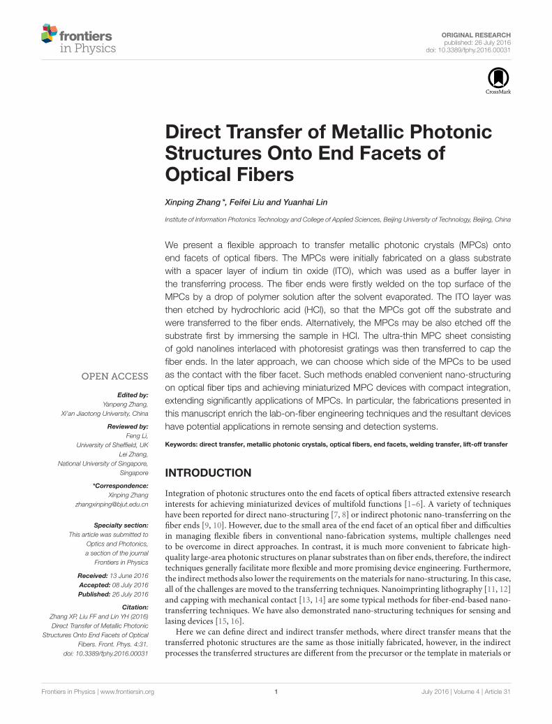
Figures 1A–C show schematically the fabrication proceduresof the MPCs using interference lithography and colloidal goldnanoparticles, as has been described in our previous publications[18–20]. Interference lithography using a UV laser at 325 nmand a positive photoresist (PR) S1805 produced grating structureswith a period of about 425 nm and a modulation depth of morethan 100 nm. Colloidal gold nanoparticles with a concentrationof 100mg/ml in xylene was spin-coated onto the PR grating. Afterthe sample was heated to about 350◦C for about 20 min, metallicgratings consisting of gold nanolines interlaced with PR lineswere produced. Figure 1D shows the SEM image of the fabricatedgold nanoline gratings, which is called as one-dimensionalMPCs and is used as the precursor for the subsequent transferprocedures.
“WELDING” TRANSFER
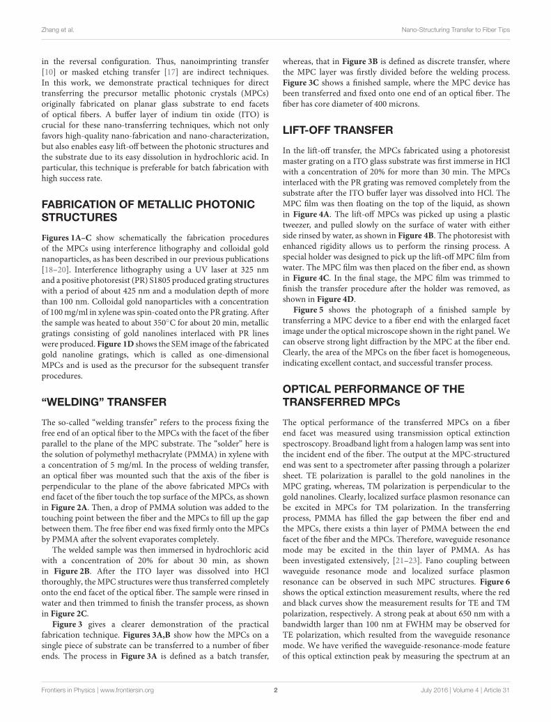
The so-called “welding transfer” refers to the process fixing thefree end of an optical fiber to the MPCs with the facet of the fiberparallel to the plane of the MPC substrate. The “solder” here isthe solution of polymethyl methacrylate (PMMA) in xylene witha concentration of 5 mg/ml. In the process of welding transfer,an optical fiber was mounted such that the axis of the fiber isperpendicular to the plane of the above fabricated MPCs withend facet of the fiber touch the top surface of the MPCs, as shownin Figure 2A. Then, a drop of PMMA solution was added to thetouching point between the fiber and the MPCs to fill up the gapbetween them. The free fiber end was fixed firmly onto the MPCsby PMMA after the solvent evaporates completely.
The welded sample was then immersed in hydrochloric acidwith a concentration of 20% for about 30 min, as shownin Figure 2B. After the ITO layer was dissolved into HClthoroughly, theMPC structures were thus transferred completelyonto the end facet of the optical fiber. The sample were rinsed inwater and then trimmed to finish the transfer process, as shownin Figure 2C.
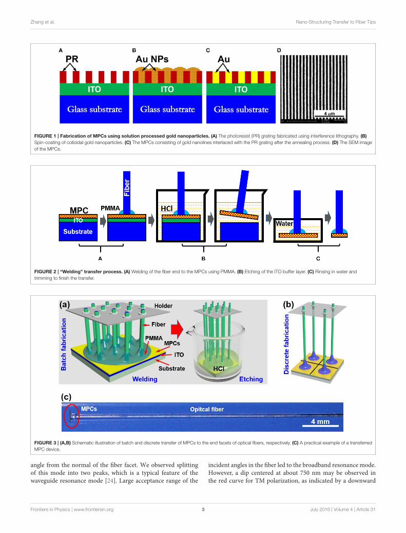
Figure 3 gives a clearer demonstration of the practicalfabrication technique. Figures 3A,B show how the MPCs on asingle piece of substrate can be transferred to a number of fiberends. The process in Figure 3A is defined as a batch transfer,
whereas, that in Figure 3B is defined as discrete transfer, wherethe MPC layer was firstly divided before the welding process.Figure 3C shows a finished sample, where the MPC device hasbeen transferred and fixed onto one end of an optical fiber. Thefiber has core diameter of 400 microns.
LIFT-OFF TRANSFER
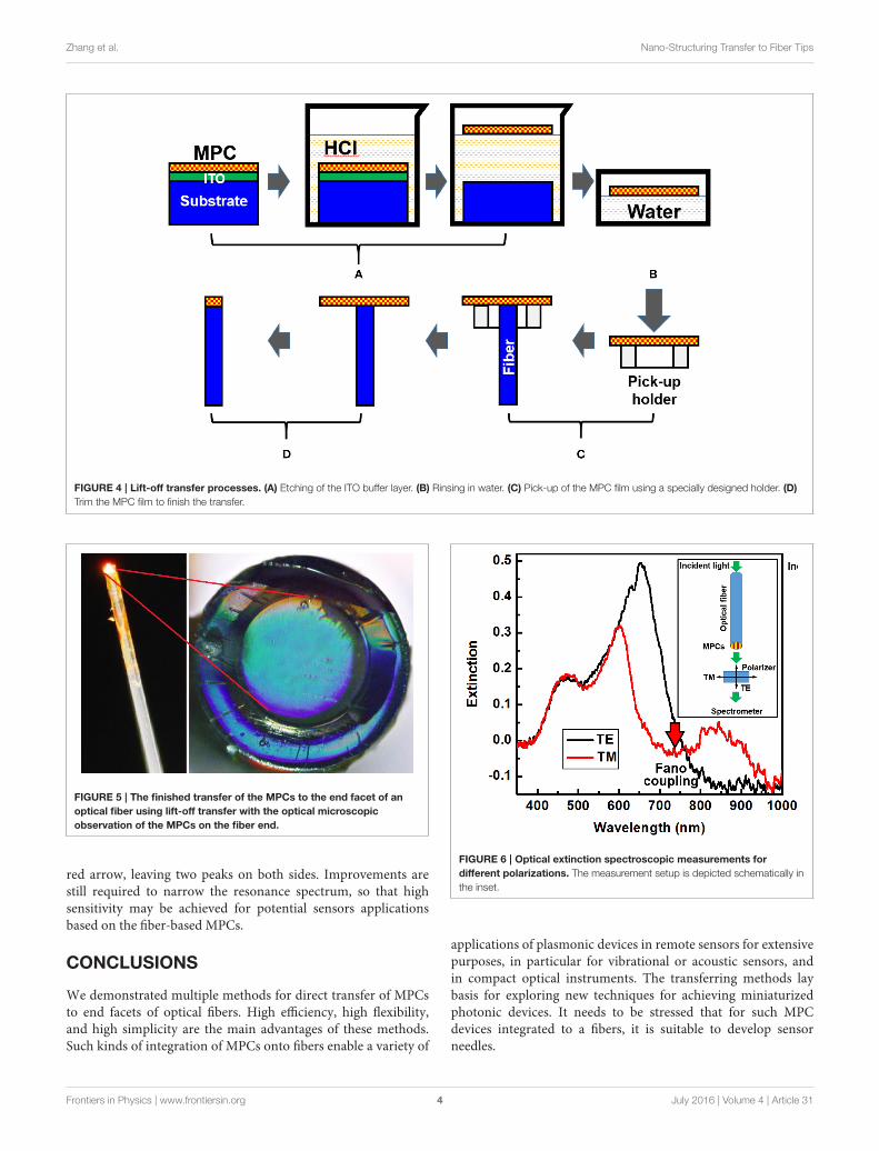
In the lift-off transfer, the MPCs fabricated using a photoresistmaster grating on a ITO glass substrate was first immerse in HClwith a concentration of 20% for more than 30 min. The MPCsinterlaced with the PR grating was removed completely from thesubstrate after the ITO buffer layer was dissolved into HCl. TheMPC film was then floating on the top of the liquid, as shownin Figure 4A. The lift-off MPCs was picked up using a plastictweezer, and pulled slowly on the surface of water with eitherside rinsed by water, as shown in Figure 4B. The photoresist withenhanced rigidity allows us to perform the rinsing process. Aspecial holder was designed to pick up the lift-off MPC film fromwater. The MPC film was then placed on the fiber end, as shownin Figure 4C. In the final stage, the MPC film was trimmed tofinish the transfer procedure after the holder was removed, asshown in Figure 4D.
Figure 5 shows the photograph of a finished sample bytransferring a MPC device to a fiber end with the enlarged facetimage under the optical microscope shown in the right panel. Wecan observe strong light diffraction by the MPC at the fiber end.Clearly, the area of the MPCs on the fiber facet is homogeneous,indicating excellent contact, and successful transfer process.
OPTICAL PERFORMANCE OF THETRANSFERRED MPCs
The optical performance of the transferred MPCs on a fiberend facet was measured using transmission optical extinctionspectroscopy. Broadband light from a halogen lamp was sent intothe incident end of the fiber. The output at the MPC-structuredend was sent to a spectrometer after passing through a polarizersheet. TE polarization is parallel to the gold nanolines in theMPC grating, whereas, TM polarization is perpendicular to thegold nanolines. Clearly, localized surface plasmon resonance canbe excited in MPCs for TM polarization. In the transferringprocess, PMMA has filled the gap between the fiber end andthe MPCs, there exists a thin layer of PMMA between the endfacet of the fiber and the MPCs. Therefore, waveguide resonancemode may be excited in the thin layer of PMMA. As hasbeen investigated extensively, [21–23]. Fano coupling betweenwaveguide resonance mode and localized surface plasmonresonance can be observed in such MPC structures. Figure 6shows the optical extinction measurement results, where the redand black curves show the measurement results for TE and TMpolarization, respectively. A strong peak at about 650 nm with abandwidth larger than 100 nm at FWHM may be observed forTE polarization, which resulted from the waveguide resonancemode. We have verified the waveguide-resonance-mode featureof this optical extinction peak by measuring the spectrum at an
Frontiers in Physics | www.frontiersin.org 2 July 2016 | Volume 4 | Article 31
Zhang et al. Nano-Structuring Transfer to Fiber Tips
FIGURE 1 | Fabrication of MPCs using solution processed gold nanoparticles. (A) The photoresist (PR) grating fabricated using interference lithography. (B)
Spin-coating of colloidal gold nanoparticles. (C) The MPCs consisting of gold nanolines interlaced with the PR grating after the annealing process. (D) The SEM image
of the MPCs.
FIGURE 2 | “Welding” transfer process. (A) Welding of the fiber end to the MPCs using PMMA. (B) Etching of the ITO buffer layer. (C) Rinsing in water and
trimming to finish the transfer.
FIGURE 3 | (A,B) Schematic illustration of batch and discrete transfer of MPCs to the end facets of optical fibers, respectively. (C) A practical example of a transferred
MPC device.
angle from the normal of the fiber facet. We observed splittingof this mode into two peaks, which is a typical feature of thewaveguide resonance mode [24]. Large acceptance range of the
incident angles in the fiber led to the broadband resonance mode.However, a dip centered at about 750 nm may be observed inthe red curve for TM polarization, as indicated by a downward
Frontiers in Physics | www.frontiersin.org 3 July 2016 | Volume 4 | Article 31
Zhang et al. Nano-Structuring Transfer to Fiber Tips
FIGURE 4 | Lift-off transfer processes. (A) Etching of the ITO buffer layer. (B) Rinsing in water. (C) Pick-up of the MPC film using a specially designed holder. (D)
Trim the MPC film to finish the transfer.
FIGURE 5 | The finished transfer of the MPCs to the end facet of an
optical fiber using lift-off transfer with the optical microscopic
observation of the MPCs on the fiber end.
red arrow, leaving two peaks on both sides. Improvements arestill required to narrow the resonance spectrum, so that highsensitivity may be achieved for potential sensors applicationsbased on the fiber-based MPCs.
CONCLUSIONS
We demonstrated multiple methods for direct transfer of MPCsto end facets of optical fibers. High efficiency, high flexibility,and high simplicity are the main advantages of these methods.Such kinds of integration of MPCs onto fibers enable a variety of
FIGURE 6 | Optical extinction spectroscopic measurements for
different polarizations. The measurement setup is depicted schematically in
the inset.
applications of plasmonic devices in remote sensors for extensivepurposes, in particular for vibrational or acoustic sensors, andin compact optical instruments. The transferring methods laybasis for exploring new techniques for achieving miniaturizedphotonic devices. It needs to be stressed that for such MPCdevices integrated to a fibers, it is suitable to develop sensorneedles.
Frontiers in Physics | www.frontiersin.org 4 July 2016 | Volume 4 | Article 31
Zhang et al. Nano-Structuring Transfer to Fiber Tips
AUTHOR CONTRIBUTIONS
XZ designed this research work, performed the fabrication andprocessed the data, and wrote the paper. FL measured themicroscopic and spectroscopic data. YL provided the 3D picturesillustrating the transferring principles.
ACKNOWLEDGMENTS
The authors acknowledge the 973 program (2013CB922404),the National Natural Science Foundation of China (11274031,11434016), and the Beijing Key Lab of Microstructure andProperty of Advanced Materials for the support.
REFERENCES
1. ChenW, HanW, Abeysinghe DC, Nelson RL, Zhan Q. Generating cylindrical
vector beams with subwavelength concentric metallic gratings fabricated on
optical fibers. J Opt. (2011) 13:015003. doi: 10.1088/2040-8978/13/1/015003
2. Ma N, Ashok PC, Stevenson DJ, Gunn-Moore FJ, Dholakia K. Integrated
optical transfection system using a microlens fiber combined with
microfluidic gene delivery. Biomed Opt Express (2010) 1:694–705. doi:
10.1364/BOE.1.000694
3. Bachelot R, Fares A, Fikri R, Barchiesi D, Lerondel G, Royer P. Coupling
semiconductor lasers into single-mode optical fibers by use of tips grown by
photopolymerization. Opt Lett. (2004) 29:1971–3. doi: 10.1364/OL.29.001971
4. Parkes W, Djakov V, Barton JS, Watson S, MacPherson WN, Stevenson JTM,
et al. Design and fabrication of dielectric diaphragm pressure sensors for
applications to shock wave measurement in air. J Micromech Microeng. (2007)
17:1334–42. doi: 10.1088/0960-1317/17/7/016
5. Kostovski G, White DJ, Mitchell A, Austin MW, Stoddart PR. Nanoimprinted
optical fibres: biotemplated nanostructures for SERS sensing. Biosens
Bioelectron. (2009) 24:1531–5. doi: 10.1016/j.bios.2008.10.016
6. Viets C, Hill W. Comparison of fibre-optic SERS sensors with differently
prepared tips. Sens Actuat B Chem. (1998) 51:92–9. doi: 10.1016/S0925-
4005(98)00170-1
7. WilliamsHE, FrepponDJ, Kuebler SM, Rumpf RC,MelinoMA. Fabrication of
three-dimensional micro-photonic structures on the tip of optical fibers using
SU-8. Opt Express (2011) 19:22910–22. doi: 10.1364/OE.19.022910
8. Feng S, Zhang X, Wang H, Xin M, Lu Z. Fiber coupled waveguide grating
structures. Appl Phys Lett. (2010) 96:133101. doi: 10.1063/1.3373422
9. Smythe EJ, Dickey MD, Whitesides GM, Capasso F. A technique to transfer
metallic nanoscale patterns to small and non-planar surfaces. ACS Nano
(2009) 3:59–65. doi: 10.1021/nn800720r
10. Kostovski G, Chinnasamy U, Jayawardhana S, Stoddart PR, Mitchell
A. Sub-15nm optical fiber nanoimprint lithography: a parallel, self-
aligned and portable approach. Adv Mater. (2011) 23:531–5. doi:
10.1002/adma.201002796
11. Jia PP, Yang J. A plasmonic optical fiber patterned by template transfer as
a high-performance flexible nanoprobe for real-time biosensing. Nanoscale
(2014) 6:8836–43. doi: 10.1039/C4NR01411A
12. Scheerlinck S, Taillaert D, Thourhout DV, Baets R. Flexible metal grating based
optical fiber probe for photonic integrated circuits. Appl Phys Lett. (2008)
92:031104. doi: 10.1063/1.2827589
13. Lipomi DJ, Martinez RV, Kats MA, Kang SH, Kim P, Aizenberg J, et al.
Patterning the tips of optical fibers with metallic nanostructures using
nanoskiving. Nano Lett. (2011) 11:632–6. doi: 10.1021/nl103730g
14. Wang B, Siahaan T, Dündar MA, Nötzel R, van der Hoek MJ, He
S, et al. Photonic crystal cavity on optical fiber facet for refractive
index sensing. Opt Lett. (2012) 37:833–5. doi: 10.1364/OL.37.
000833
15. Feng SF, Darmawi S, Henning T, Klar PJ, Zhang XP. A miniaturized sensor
consisting of concentric metallic nanorings on the end facet of an optical fiber.
Small (2012) 8:1937–44. doi: 10.1002/smll.201102290
16. Li ST, Wang L, Zhai TR, Xu ZY, Wang YL, Wang JY, et al. Plasmonic
random laser on the fiber facet. Opt Express (2015) 23:23985–91. doi:
10.1364/OE.23.023985
17. Smythe EJ, Dickey MD, Bao J, Whitesides GM, Capasso F. Optical antenna
arrays on a fiber facet for in situ surface-enhanced Raman scattering detection.
Nano Lett. (2009) 9:1132–8. doi: 10.1021/nl803668u
18. Zhang XP, Liu HM, Feng SF. Solution-processible fabrication of large-
area patterned and unpatterned gold nanostructures. Nanotechnology (2009)
20:425303. doi: 10.1088/0957-4484/20/42/425303
19. Zhang XP, Sun BQ, Guo HC, Tetreault N, Giessen H, Friend RH. Large-
area two-dimensional photonic crystals of metallic nanocylinders based
on colloidal gold nanoparticles. Appl Phys Lett. (2007) 90:133114. doi:
10.1063/1.2717567
20. Zhang XP, Sun BQ, Guo HC, Nau D, Giessen H, Friend RH. Metallic photonic
crystals based on solution-processible gold nanoparticles. Nano Lett. (2006)
6:651–5. doi: 10.1021/nl052361o
21. Christ A, Tikhodeev SG, Gippius NA, Kuhl J, Giessen H. Waveguide-
plasmon polaritons: strong coupling of photonic and electronic resonances
in a metallic photonic crystal slab. Phys Rev Lett. (2003) 91:1839011. doi:
10.1103/PhysRevLett.91.183901
22. Zhang XP, Ma XM, Dou F, Zhao PX, Liu HM. A biosensor based on metallic
photonic crystals for the detection of specific bioreactions. Adv Funct Mater.
(2011) 21:4219–27. doi: 10.1002/adfm.201101366
23. Zhang XP, Dou F, Liu H. Molecular concentration sensor based on the
diffraction resonance mode of gold nanowire gratings.Nanotechnology (2010)
21:335501. doi: 10.1088/0957-4484/21/33/335501
24. Rosenblatt D, Sharon A, Friesem AA. Resonant grating waveguide
structures. IEEE J Quantum Electron. (1997) 33:2038–59. doi: 10.1109/3.
641320
Conflict of Interest Statement: The authors declare that the research was
conducted in the absence of any commercial or financial relationships that could
be construed as a potential conflict of interest.
Copyright © 2016 Zhang, Liu and Lin. This is an open-access article distributed
under the terms of the Creative Commons Attribution License (CC BY). The use,
distribution or reproduction in other forums is permitted, provided the original
author(s) or licensor are credited and that the original publication in this journal
is cited, in accordance with accepted academic practice. No use, distribution or
reproduction is permitted which does not comply with these terms.
Frontiers in Physics | www.frontiersin.org 5 July 2016 | Volume 4 | Article 31