Embed Size (px)
Citation preview

Journal of Physics Conference Series
OPEN ACCESS
Discrimination of wireless electromagnetic signalsby electro-optic modulators using an array of patchantennas embedded with orthogonal gapsTo cite this article Yusuf Nur Wijayanto et al 2012 J Phys Conf Ser 379 012017
View the article online for updates and enhancements
You may also likePlasma As a ComplimentaryElectrochemical Reaction Process for ThinFilm Deposition in Preparing EnergyConversion and Storage DevicesYue Kuo
-
Water Motion Safety Recognition andMonitoring System Based on the WirelessSignal TransmissionGuobiao Yang Qiuping Yi Zhao Wang etal
-
(Invited) From Carbon Nanotubes toGraphene a Versatile Building Block inthe Nanoscale WorldCarter Kittrell and James M Tour
-
This content was downloaded from IP address 1211641143 on 16112021 at 1108
Discrimination of wireless electromagnetic signals by electro-
optic modulators using an array of patch antennas embedded
with orthogonal gaps
Yusuf Nur Wijayanto Hiroshi Murata and Yasuyuki Okamura
Graduate School of Engineering Science Osaka University
1-3 Machikaneyama Toyonaka Osaka 560-8531 Japan
E-mail wijayantoeceeesosaka-uacjp
Abstract We proposed a new wireless electromagnetic signal discrimination device using
electro-optic modulators and an array of planar patch antennas embedded with orthogonal
gaps Wireless electromagnetic signals can be detected and converted directly to lightwave
signals through optical modulation The magnitude phase and polarization of the wireless
signal can be measured precisely and identified By using meandering gap structures the
directivity of the wireless signal conversion can be tuned more precisely Furthermore the
directivity of the wireless signal conversion in two-dimensional space can also be obtained by
comparing two orthogonal modulated lightwave signals from two orthogonal optical
waveguides The design and analysis of the device and experiments at an operational frequency
of 26 GHz are presented
1 Introduction
Wireless-fibre technologies with low power consumption have been developed to establish a
sustainable society Wireless technologies provide convenience mobility and flexibility for users [1]
However the wireless microwave signals are easily affected by environmental noise and high
transmission loss Their allocated bandwidth is relatively narrow On the other hand optical fibre
technologies provide large bandwidth low transmission loss no inductance and no interference [2]
The combination of wireless microwave and optical fibre technologies has been developed in order to
exploit their advantages The combined technologies can be used for communication remote sensing
electromagnetic compatibility testing identification and so on
Conversion between wireless microwave and lightwave signals is important in wireless-fiber systems
which can be obtained using optical modulators and optical detectors with microwave antennas
Several converters composed of discrete optical modulators and discrete antennas have been reported
[3-4] The attenuation of the received signal through the cable becomes a problem in high-frequency
operation Electro-optic (EO) converters using antenna-coupled optical modulation electrodes were
also proposed for high-frequency operation with low distortion [5-8] They are composed of antennas
resonant electrodes and connection lines Good impedance matching conditions and precise frequency
tuning between the planar structures are required in order to obtain effective optical modulation
However complete matching and precise tuning are rather difficult
We have proposed EO wireless-optical converters using patch antennas embedded with a narrow gap
[910] The devices are composed of only patch antennas and there are no other planar elements on the
ECO-MATES 2011 IOP PublishingJournal of Physics Conference Series 379 (2012) 012017 doi1010881742-65963791012017
Published under licence by IOP Publishing Ltd 1
substrate The proposed devices have simple compact structures and are operated with no precise
tuning and no external power supply Optical modulation with extremely low distortion was
demonstrated We have also proposed EO wireless-optical converters using patch antennas embedded
with orthogonal gaps for dual-polarized wireless signal detection [11] However the modulation index
was low owing to the limitation by the lightwave transit-time effect [12 13]
In the present paper a new EO modulator using planar patch antennas embedded with orthogonal gaps
is proposed for wireless signal discrimination The modulation index of the proposed devices can be
enhanced by approximately three times by adding a number of the patch antennas in array form using
a new design for the compensation of the transit-time effects The magnitude and phase of the wireless
signal is obtainable at the same time The wireless directivity in the one-dimensional (1-D) plane and
two-dimensional (2-D) space can also be tuned by meandering gap structures for phase-reversal
Therefore the wireless electromagnetic signals can be identified and discriminated using the proposed
device
In the following sections we will discuss the proposed device structure and analyze its characteristics
in detail The preliminary experimental results and advanced measurement setup for identifying
wireless signals are also presented
2 Device structures
(a)
(b) (c)
Figure 1 (a) Basic structure of the wireless signal discrimination device using a
combination of patch antennas with gaps the entire device structure (b) the patch
antenna with a gap and (c) the patch antenna with orthogonal gaps
Figure 1 shows the basic structure of the proposed device which is fabricated on an EO crystal
substrate The proposed device is composed of two orthogonal optical waveguides one patch antenna
with orthogonal gaps and four patch antennas with a single gap The length L of each patch antenna
is set as a half wavelength for the designed wireless electromagnetic signal The patch antenna with
orthogonal gaps is set at the centre of the device where the size is set to LxL The patch antennas with
a single gap are set surrounding the patch antenna with orthogonal gaps where the size is set to LxW
The width W of the patch antennas with a single gap can be set to be longer than a half wavelength
but slightly shorter than one wavelength of the microwave signal in order to avoid unwanted higher-
order mode effects The width of the gaps is of micrometer order The orthogonal optical waveguides
are located under the edge of the gaps A buffer layer is inserted between the substrate and the
antennas The reverse side of the substrate is covered with a ground electrode
ECO-MATES 2011 IOP PublishingJournal of Physics Conference Series 379 (2012) 012017 doi1010881742-65963791012017
2
When a wireless signal at the design frequency with an arbitrary polarization is irradiated to the
proposed device a resonant standing-wave microwave current is induced on the patch antenna surface
The induced current can be separated into two components along the x- and y-axes In the proposed
device displacement currents are induced across the gap G1 normal to the x-axis and the gap G2
normal to the y-axis due to the continuity of the current flow As a result strong electric fields are also
induced across the gaps The strong electric field across the gaps can be used for optical modulation
Therefore the wireless signal can be converted to the lightwave signal through optical modulation by
the induced electric field across the gaps The modulated lightwaves are obtained from two orthogonal
optical waveguides The magnitude and phase of the wireless signal can be obtained by detecting the
modulated lightwaves The polarization of the wireless signal can also be identified by comparing the
two orthogonal modulated lightwaves Furthermore the directivity of the wireless signal conversion is
precisely controllable using meandering gap structures to compensate for the degradation of the
optical modulation owing to the transit-time effect Therefore the wireless signals with different
irradiation angles can be discriminated through optical modulation using the proposed device
3 Patch antennas
31 Patch antenna with a single gap
The patch antenna with a gap shown in Figure 1(b) is considered This antenna has a gap G1 parallel
to the y-axis When a wireless electromagnetic signal with a polarization in the x-axis is irradiated to
the patch antenna with a normal irradiation angle a standing-wave electromagnetic surface current is
induced on the patch antenna along the x-axis [14-17] The induced surface current along the x-axis
Kx can be expressed
Λ= xptKtxK
m
mxpx
πω
2cos)cos()( (1)
where Kxp is the amplitude of the surface current along the x-axis ωm is the wireless microwave signal
angular frequency and Λm is the microwave wavelength The patch antenna length L is set to the half
wavelength of the wireless electromagnetic signal when the fundamental mode is induced at the
resonant frequency ie p = 1 In a standard patch antenna with no gap the surface current for the
fundamental mode becomes maximum at x = 0 along the x-axis
In the patch antenna with a narrow gap the displacement current must be induced across the gap for
the current continuity requirement [18-20] The induced electric field Ex across the gap is obtained by
time integration of the displacement currents as
)sin()0()0(1
)0(1
tKdttKtDtEmxxxx
ωε
=prop= int (2)
where D is the electric flux density ( ED ε= ) and ε is the permittivity The strong electric field across
the gap can be used for optical modulation
The analysis of the patch antenna with the gap G2 parallel to the x-axis can be obtained using a
similar procedure When a wireless electromagnetic signal with polarization along the x-axis is
irradiated to the patch antenna a standing-wave electromagnetic surface current is induced on the
patch antenna along the y-axis The standing-wave electromagnetic surface current Ky along y-axis
and the induced electric field Ey across the gap for the half-wavelength patch antennas are expressed
as
Λ+= ytKtyK
m
myy
πϕω
2cos)cos()(
1 (3)
)sin()0()0(1
)0(1
ϕωε
+=prop= int tKdttKtDtEmyyyy (4)
ECO-MATES 2011 IOP PublishingJournal of Physics Conference Series 379 (2012) 012017 doi1010881742-65963791012017
3
where Ky1 is the amplitude of the surface current along the y-axis and ϕ is the mutual phase shift
between the x- and y-current components
An arbitrary polarization of the wireless signal can be also analyzed The standing-wave current
surface can be separated into two components along the x- and y-axes Therefore strong electric fields
are induced across the two orthogonal gaps in both patch antennas
32 Patch antenna with orthogonal gaps
A patch antenna with two orthogonal gaps is shown in Figure 1(c) the size of which was set to be LxL
for receiving dual polarization wireless signals When a wireless electromagnetic signal with an
arbitrary polarization is irradiated to the patch antenna with a normal irradiation angle a standing-
wave electromagnetic surface current is induced on the patch antenna along the x- and y-axes The
standing-wave electromagnetic surface currents Kx and Ky along the x- and y-axes can be expressed
by Equations (1) and (3) respectively Then displacement currents must be induced across both gaps
in order to satisfy the current continuity requirement Therefore the induced electric fields across the
gap Ex and Ey are obtained These electric fields can be also expressed by Equations (2) and (4)
respectively The strong electric field across the two gaps can be also used for optical modulation
By measuring the modulation indices and phases the polarization of the wireless signal can be
identified completely
33 Numerical analysis
The field distributions on the surfaces of the patch antennas were analyzed using HFSS 3-D
electromagnetic field analysis software Figure 2 shows the calculated electric field distributions on
the substrate surface when microwave signals with different polarization conditions are irradiated to
the device
(a) (b) (c)
(d) (e) (f)
Figure 2 (a) Top view of the patch antenna array Field distributions in the z-component on
the substrate surface with the polarization at (b) 0 degrees (c) 30 degrees (d) 45 degrees (e)
60 degrees and (f) 90 degrees
First when the wireless signal with a linear polarization along the x-axis (0 degrees) is irradiated to the
patch antenna array as shown in Figure 1(a) a strong electric field is induced across the gap G1
E
E
E E
E
ECO-MATES 2011 IOP PublishingJournal of Physics Conference Series 379 (2012) 012017 doi1010881742-65963791012017
4
normal to the x-axis and a negligible electric field is induced across the other gap G2 parallel to the x-
axis as shown in Figure 2(b) When a linear polarized wireless signal with an angle of 30 degrees to
the x-axis is irradiated to the device strong electric fields are induced across both orthogonal gaps as
shown in Figure 2(c) However the magnitudes of the electric fields across the gaps are different
Then when a linear polarized wireless signal with an angle of 45 degrees to the x-axis is irradiated to
the device strong electric fields are induced across both orthogonal gaps with almost the same
magnitude as shown in Figure 2(d) Figure 2(e) shows the electric field distribution when the wireless
signal with the 60-degree polarization condition is irradiated to the device The electric field
magnitudes along the gaps are the inverse of those for the 30-degree polarization condition Finally
when the polarization condition of the radiated wireless signal is rotated 90 degrees (along the y-axis)
a strong electric field is induced across the gap G2 normal to the y-axis and a negligible electric field
is induced across the gap G1 parallel to the y-axis as shown in Figure 2(f) Using these
characteristics the linear polarization condition of the wireless signals can be identified
Furthermore when a microwave signal with circular polarization states is irradiated to the device the
induced electric fields across all gaps have the same magnitude but their phases differ by 90 degrees
between the x- and y-axes Therefore the circular polarization of the wireless signals can be measured
using the proposed device
4 Optical modulation
41 Transit-time effect
In order to calculate modulation indices through the EO effect the microwave electric field that would
be observed by the lightwave propagating in the optical waveguides should be considered while taking
the transit-time effect into account
The transformation for considering the transit-time effect for a lightwave propagating in the optical
waveguide WG1 along the y-axis can be expressed by tvyyg1
minus= where yrsquo denotes the point of the
lightwave in the coordinate system moving with the lightwave and vg is the group velocity of the
lightwave Therefore the microwave electric fields would be observed by the lightwave propagating
along the waveguide WG1 at the h-th patch antenna in the array structure become
minus==
1
)(
g
x
opt
xv
yytEyE
minus+
minusprop
10
1
0sin)1(
sin θω yknhd
v
yyK
my
g
mx
)sin)1(sin(11010
ζθ +minus+= yknhdynkKymgmx (5)
where ng1 is the group index of the lightwave propagating in the waveguide WG1 (ng1 = cvg1) ζ is the
initial phase of the lightwave in waveguide WG1 (ζ = km ng1 yrsquo) and d is the distance of each unit cell
Using a similar method the microwave electric fields that would be observed by the lightwave
propagating Eopt
along waveguide WG2 in the unit cell device is expressed as
)sin)1(sin()(22020
ϕζθ ++minus+= xknhdxnkKxExmgmy
opt
y (6)
where ng2 is the group index of the lightwave propagating in WG2 (ng2 = cvg2) and ζ2 is the initial
phase of the lightwave in WG2 (ζ2 = km ng2 xrsquo)
42 Modulation index
The lightwaves propagating in the orthogonal optical waveguides WG1 and WG2 are modulated by
the induced electric field across gaps G1 and G2 through optical modulation The phase-modulated
lightwaves by the wireless signal are obtained The modulation indices ∆φ1 and ∆φ2 of the phase-
ECO-MATES 2011 IOP PublishingJournal of Physics Conference Series 379 (2012) 012017 doi1010881742-65963791012017
5
modulated lightwaves can be determined taking into account the overlapping between of the induced
electric fields across the gaps and the lightwave in the cross section which are expressed as
++Γ=∆ intintint
+
minusminus
+minus
minusminus
23
23
2
2
23
23
3
33
11)()()()(
Wd
Wd
opt
x
L
L
opt
x
Wd
Wd
opt
x
e dyyEdyyEdyyEnr
WGλ
πθφ (7)
++Γ=∆ intintint
+
minusminus
+minus
minusminus
23
23
2
2
23
23
3
33
22)()()()(
Wd
Wd
opt
y
L
L
opt
y
Wd
Wd
opt
y
e dxxEdxxEdxxEnr
WGλ
πθφ (8)
where λ is the wavelength of lightwave propagating in the optical waveguides r33 is the EO
coefficient ne is the extraordinary refractive index of the substrate Γ is a factor expressing the
overlapping between the induced microwave electric field and the lightwave and L and W are the
lengths of the patch antenna
The modulation indices ∆φ1 and ∆φ2 are function of the irradiation angle of the wireless signal as
shown in Equations (7) and (8) respectively These indices contain information of the irradiation
angle of the wireless signal along the yz- and xz-planes independently The 1-D directivities of the
wireless electromagnetic signal using the proposed device can be obtained The directivity can be
tuned using meandering gap structures for phase-reversal
43 Phase-reversal
The degradation of the optical modulation can be compensated by phase-reversal by considering the
transit-time effect As a result of the electric field distribution the direction of the z-component of the
electric field under the gap edge is reversed between the edges The characteristics of the z-component
can be used for phase-reversed structures We have proposed an EO wireless-optical converter using
quasi-phase-matching array of patch antennas with a gap [13] The degradation of the optical
modulation can be compensated for by shifting the position of the patch antennas with a gap along the
optical waveguide The device has been worked properly to increase the modulation index
(a) (b) (c)
Figure 3 (a) Patch antenna with a meandering gap (b) cross-sectional view along line-A
and (c) cross-sectional view along line-B
Here phase reversal by meandering gap structures is proposed The degradation of the optical
modulation with tuning for several wireless irradiation angles can be obtained using meandering gap
structures The typical structure of patch antennas with a meandering gap is shown in Figure 3 The
cross-sectional views for the structures A and B are also shown in Figures 3(b) and 3(c) respectively
The directions of the electric fields across the optical waveguide are reversed along the z-component
Therefore control of the modulation polarity along the optical waveguide is obtainable These
characteristics are very useful for the design of the directivity in the array structures
5 Experiments As a preliminary experiment a prototype device composed of only patch antennas embedded with
orthogonal gaps was designed and fabricated The prototype device was designed at a 26-GHz
microwave operational frequency using a 04-mm-thick z-cut LiTaO3 crystal The patch antennas were
08-mm squares having 5-microm-wide gaps at the centre In the device 4x4 patch antennas were aligned
with a separation of 55 mm
ECO-MATES 2011 IOP PublishingJournal of Physics Conference Series 379 (2012) 012017 doi1010881742-65963791012017
6
In the device fabrication 4x4 channel optical waveguides for single-mode operation at a wavelength
of 155 microm was fabricated in 12 hours using the annealed proton-exchange method with benzoic acid
at 513 K [2122] A thin SiO2 buffer layer was deposited on the surface of the substrate after optical
waveguide fabrication Then patch antennas with gaps were fabricated using a 1-microm-thick aluminium
film on the buffer layer by thermal vapour deposition a standard photolithography technique and a
lift-off process The edges of the gaps were placed on the optical waveguides for efficient conversion
Thermal annealing at 623 K was also performed for 1 hour in order to increase the optical waveguide
performance Finally a 1-microm-thick aluminium film was deposited on the reverse side of the substrate
as a ground electrode
In the device measurement two lightwaves of 155 microm in wavelength from a distributed-feedback
laser were coupled to the fabricated device A wireless microwave signal of 200 mW from a
microwave signal generator was irradiated to the fabricated device using a horn antenna The light
output spectra were observed and monitored using an optical spectrum analyzer
The measured lightwave spectra are shown in Figures 4(a) and 4(b) when the polarization of the
microwave signal was set to 0 degrees (x-polarization) In this case optical sidebands were clearly
observed in the output lightwave from the optical waveguide WG1 and no optical sideband was
observed from the waveguide WG2 as shown in Figures 4(a) and 4(b) Furthermore Figure 5 shows
the measured optical modulation for the wireless irradiation angle dependence The experimental
results approximately coincided with the calculation results
(a) (b)
Figure 4 Measured lightwave output spectra from optical waveguides (a) WG1 and (b)
WG2 when the wireless electromagnetic signal polarization was set to be 0 degrees
Figure 5 Measured optical
modulation for the wireless
irradiation angle dependence
Based on the measurement results the basic operations of the device were successfully confirmed The
polarization of the wireless electromagnetic signal can be identified The magnitude of the wireless
electromagnetic signal can be also measured The 1-D directivity of the wireless signal conversion was
also measured and confirmed
ECO-MATES 2011 IOP PublishingJournal of Physics Conference Series 379 (2012) 012017 doi1010881742-65963791012017
7
6 Advanced device for 2-D directivity
61 Design
In order to realize more advanced functionality with 2-D directivity for discriminating space-division-
multiplexed (SDM) or multiple-input-multiple-output (MIMO) wireless signals a new device using an
MxN array of the proposed device is also proposed as shown in Figure 6 The device is composed of
MxN orthogonal optical waveguides and an MxN array of patch antennas embedded with gaps as
shown in Figure 1(a) (dashed-line area in Figure 6) The optical waveguide is placed under the edge of
the gaps for effective modulation
Figure 6 Wireless signal discrimination device using MxN orthogonal optical waveguides
and patch antennas with gaps where the dashed-line area is as shown in Figure 1(a)
(a) (b)
Figure 7 (a) Several patterns of patch antenna arrays with meandering gap structures where the
thick line is Eopt
with phase-reversed structures and (b) the calculation results for the proposed
device according to the directivity in 1-D using the meandering gap patterns
When the polarization of the wireless signal at 45 degrees is irradiated to the device with an arbitrary
wireless irradiation angle strong electric fields are induced across all gaps with same magnitude
ECO-MATES 2011 IOP PublishingJournal of Physics Conference Series 379 (2012) 012017 doi1010881742-65963791012017
8
strength The induced electric fields can be converted to lightwaves through optical modulation Using
meandering structures the degradation of the optical modulation can be compensated for by tuning the
directivity The effective optical modulation function of the irradiation angle of the wireless signal can
be obtained by modifying Equations (7) and (8) for several array structures The electric field that
would be observed by the lightwave should be considered
In the device design the parameters were set as follows fm = 26 GHz no = 1 ng = 21 d = 55 mm L
= 08 mm and M = N = 5 First considering the 1-D directivity of the wireless signal conversion the
patch antennas with meandering gap structures for several wireless signal angles are shown in Figure
7(a) The calculation results with the meandering gap structures are shown in Figure 7(b) for 1-D
directivity analysis The 1-D directivity was analyzed independently along the yz-plane (θ2) and the
xy-plane (θ1)
62 Analysis
Based on the designed 1-D directivity of the wireless signal conversion the 2-D directivity can be
obtained by considering the two orthogonal modulated lightwaves The 2-D directivity can be
measured by multiplying or comparing the modulated lightwaves
(a) (b) (c)
Figure 8 Calculated 2-D directivity of the wireless signal conversion for wireless irradiation
angles of (a) θ1 = θ2 = 0 degrees (b) θ1 = θ2 = 30 degrees and (c) θ1 = θ2 = -15 degrees
Figure 8 shows the typical calculated 2-D directivity of the wireless signal conversion in the xy-plane
for several wireless irradiation angles The first combination of the two orthogonal modulated lights
was set to be effective for the normal wireless irradiation angle as shown in Figure 8(a) The other
combinations of the orthogonal modulated lights for wireless irradiation angle in the xz-plane (θ2) and
the yz-plane (θ1) are shown in Figure 8(b) for θ1 = θ2 = 30 degrees and Figure 8(c) for θ1 = θ2 = -15
degrees The proposed device has MxN 2-D directivity combinations of the wireless signal conversion
according to the number of orthogonal modulated lightwaves Therefore the proposed device can be
used for discriminating the wireless electromagnetic signals
7 Conclusion
The discrimination of the wireless electromagnetic signal by EO modulators using planar patch
antennas embedded with orthogonal gaps was proposed The wireless signal can be received
separated and converted to a lightwave directly and simultaneously using the device The directivity
of the wireless signal conversion can be tuned by controlling the phase reversal with meandering gap
structures The typical basic operations of the device were demonstrated successfully The magnitude
phase and polarization of the wireless signals can be measured and identified through optical
modulation The discrimination directivity of the wireless signal in two-dimensional space can be
obtained by considering the two orthogonal modulated lightwaves The proposed device can be
applied to SDM MIMO wireless signals and electromagnetic compatibility test systems
ECO-MATES 2011 IOP PublishingJournal of Physics Conference Series 379 (2012) 012017 doi1010881742-65963791012017
9
At present we are attempting to demonstrate and measure the performance of the device in wireless-
over-fibre links
Acknowledgments
The authors would like to thank Drs H Shiomi and K Kitatani for their valuable advice and
comments regarding the analysis and discussion The present study was supported in part by a Grant-
in-Aid for Scientific Research and a grant from the Osaka University Global COE Program ldquoCenter
for Electronics Device Innovationrdquo both from the Ministry of Education Culture Sports Science and
Technology (MEXT) of Japan
References
[1] Ramirez-Iniguez R Idrus S M Sun Z 2008 Optical Wireless Communications IR for Wireless
Connectivity (Florida CRC Press)
[2] Iezekiel S 2009 Microwave Photonics Device and Applications (Chichester John Wiley amp Sons)
[3] Kawanishi T Oikawa S Higuma K Sasaki M Izutsu M 2002 IEICE Trans Electron E85-C 1
[4] Murphy T E and Pagan V R Phase Modulated Radio-Over-Fiber Link with Electro-Optic Down
Conversion Using a Delay-Line Interferometer Proc SPIE (San Francisco USA 2011) 7936
79360L doi10111712875695
[5] Sheehy F T Bridges W B and Schaffner J H 1993 IEEE Photon Tech Lett 5 3
[6] Bridges W B Burrows L J Cummings U V Schaffner J H Scherer A and Sheehy F T Antenna-
Coupled Millimeter-Wave Electro-Optic Modulators For 20 to 100GHz Proc International
Topical Meeting on Microwave Photonics (Kyoto Japan Dec 1996) pp 21-24
[7] Shinada S Kawanishi T and Izutsu M 2007 IEEE Trans Electron E90-C 5
[8] Murata H Miyanaka R and Okamura Y Millimeter-Wave Wireless Signal Discrimination Device
Using Electro-Optic Modulator with Antenna-Coupled Electrodes and Polarization-Eeversed
Structures of Ferroelectric Optical Crystal Proc 41st European Microwave Conference
(Manchester UK October 2011) pp EuMCEuMIC11-1
[9] Wijayanto Y N Murata H and Okamura Y 2011 Novel Electro-Optic Microwave-Lightwave
Converters Utilizing a Patch Antenna Embedded with a Narrow Gap IEICE Electron Express 8 7
[10] Wijayanto Y N Murata H and Okamura Y 2012 Electron Lett 48 1
[11] Wijayanto Y N Murata H and Okamura Y 2011 Passive Electromagnetic Field Sensors Using
Electro-Optic Crystals with Metal Planar Antennas and Narrow Gaps Proc Int Sym Materials
Science and Innovation for Sustainable Society ECO-MATES (Osaka Japan Nov 2011) pp PT
7-13
[12] Murata H Matsunaga S Enokihara A and Okamura Y 2005 Electron Lett 41 8
[13] Yariv A 1989 Quantum electronics (New York Wiley)
[14] Balanis C A 1997 Antenna Theory Analysis and Design (New York John Wiley amp Sons Inc)
[15] Garg R Bartia P Bahl I and Ittipiboon A 2001 Microstrip Antenna Design Handbook (Norwood
Artech House Inc)
[16] Bahl I J and Bhartia P 1980 Microstrip Antennas (Dedham Artech House)
[17] Gupta V R and Gupta N 2004 Microwave and Optical Tech Lett 40 2 pp 158-160
[18] Gupta K C Garg R Bahl I and Bhartia P 1996 Microstrip Lines and Slotlines (Norwood Artech
House)
[19] Zhang K and Li D 2008 Electromagnetic Theory for Microwaves and Optoelectronics (Berlin
Heidelberg Springer-Verlag)
[20] Fitzpatrick R 2008 Maxwellrsquos Equation and the Principles of Electromagnetism (Hingham
Infinity Science Press)
[21] Savatinova I Tonchev S Todorov R Armenise M N Passaro V M N and Ziling C C 1996
Journal of Lightwave Tech 14 3 pp 403-409
[22] Tada K Murai T Nakabayashi T Iwashima T and Ishikawa T 1987 Japanese Journal of Applied
Physics 26 1 3 pp 503ndash504
ECO-MATES 2011 IOP PublishingJournal of Physics Conference Series 379 (2012) 012017 doi1010881742-65963791012017
10
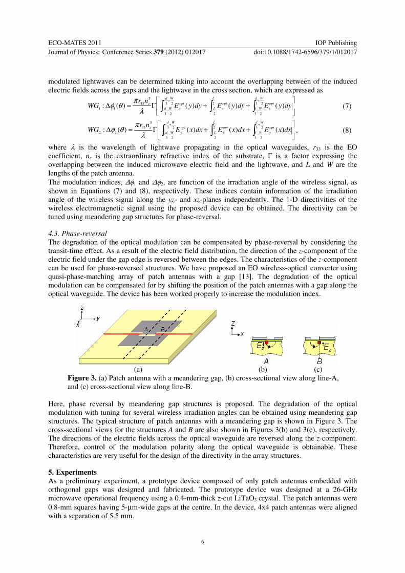