Embed Size (px)
Citation preview

DISSERTATION
IMPACT OF LIFETIME VARIATIONS AND SECONDARY BARRIERS ON
CdTe SOLAR-CELL PERFORMANCE
Submitted by
Jun Pan
Department of Physics
In partial fulfillment of the requirements
For the Degree of Doctor of Philosophy
Colorado State University
Fort Collins, Colorado
Summer 2007

ii
COLORADO STATE UNIVERSITY
June 21, 2007
WE HEREBY RECOMMEND THAT THE DISSERTATION PREPARED UNDER
OUR SUPERVISION BY JUN PAN ENTITLED “IMPACT OF LIFETIME
VARIATIONS AND SECONDARY BARRIERS ON CdTe SOLAR-CELL
PERFORMANCE” BE ACCEPTED AS FULFILLING IN PART REQUIREMENTS
FOR THE DEGREE OF DOCTOR OF PHILOSOPHY.
Committee on Graduate Work
Advisor
Department Head

iii
ABSTRACT OF DISSERTATION
Impact of Lifetime Variations and Secondary Barriers on CdTe Solar-cell
Performance
The thin-film CdTe solar cell (generally n-CdS/p-CdTe) is one of the leading
candidates for terrestrial photovoltaic applications due to its low cost and high
efficiency. However, compared with single-crystal cells of comparable band gap,
there remains a significant voltage difference, where the best CdTe cells are about
250 mV below the best GaAs cells when an appropriate adjustment is made for
bandgap. Therefore, the fabrication of high-voltage CdTe solar cells is one of the
major and critical challenges in recent years. From a device-physics point of view,
variations in carrier lifetime, carrier (hole) density, and other aspects such as a back
electron reflector, should be able to improve the voltage and efficiency.
This dissertation systematically studies the impact of lifetime variations and
secondary barriers on CdTe solar-cell performance. Numerical simulation is used to
evaluate how combinations of lifetime, carrier density, interfacial recombination, and
back barriers affect cell behaviors. Strategies to improve voltage and cell performance
are explored. The experimentally observed characteristics with significant back-
contact barrier (back-hole barrier) are explained. Current-voltage distortion which
would result from a front barrier is also discussed.

iv
In the absence of secondary barriers, higher voltage and fill factor should be
obtained, but only by a moderate amount, when the carrier lifetimes are increased
from today’s typical value (0.5 ns). Similarly, increased hole density (above the
typical 2 × 1014 cm-3) should lead to higher voltage, but with today’s lifetimes, low
collection outside the depletion region will lead to a drop in the current. Hence, both
higher lifetime and higher carrier density are needed to obtain significantly higher
voltage.
The effect of lifetimes with secondary back barriers is also explored. The
combination of a significant back-hole barrier and a typical CdTe carrier density leads
to two competing mechanisms that can alter the J-V characteristics in two different
ways depending on the lifetime. One is a hole limitation on current in forward bias,
which reduces fill-factor and efficiency. The second is a high electron contribution to
the forward diode current, which results in a reduced voltage. CdTe solar cells are
particularly prone to the latter, since the combination of a wide depletion region and
impedance of light-generated holes at the back contact increases electron injection at
the front diode. Simulated J-V curves illustrating the two major effects are in good
agreement with experimental curves that have been observed in recent years.
When an effective electron reflector is present at the back contact, the voltage
should be increased because of the reduced voltage-limiting back recombination, and
the lifetimes for high efficiency need not to be particularly high. A fully depleted
CdTe layer (hole density of 2 × 1013 cm-3) with such a back-electron reflector and
moderate lifetime should significantly increase voltage. The electron reflector could
of course be applied to CdTe that is not fully depleted. In this case, the benefit is

v
relatively small when the lifetime is moderate, because the carrier densities at the
back would not be large enough for back recombination to significantly lower the
voltage.
A secondary front barrier in CdS/CdTe solar cell may block the electron
current at both directions in the front. There are several possible causes for such a
front barrier: high conduction-band offset (CBO) between TCO and CdS, highly
photoconductive CdS layer, or a dipole CdS on the p-type CdTe layer. Numerical
simulations show that high front barrier caused by dipole CdS may result in fill-factor
and efficiency losses, thus J-V distortion. The maximum energy difference between
the conduction band and the quasi-Fermi level for electrons in the front is the key
parameter.
Jun Pan
Department of Physics
Colorado State University
Fort Collins, CO 80523
Summer 2007

vi
Acknowledgements
Grateful acknowledgment is expressed to Colorado State University for giving
me the opportunity to work and study as a part of the graduate program.
I am so thankful for all individuals who help me reach this point in my life,
although I only acknowledge a few people here. Sincere appreciation is extended to
all my committee members, including Prof. James Sites, Prof. Carl Patton, Prof.
Marty Gelfand, and Prof. Carmen Menoni. My sincerest gratitude is expressed to
Prof. Sites for serving as my advisor. He gave me many suggestions, encouragement,
and support throughout my research work, and showed me how to formulate
scientific ideas, carry out productive research, publish scientific work, and write this
dissertation.
I would like to thank Prof. Alan. Fahrenbruch for all scientific discussions and
suggestions which were very important in my research.
I also thank all the graduate students who worked or are still working in
CSU’s photovoltaic lab: Dr. Alex Pudov, Dr. Markus Gloeckler, Dr. Samuel Demtsu,
Dr. Caroline Corwine, Tim Nagle, Alan Davies, Ana Kanevce, and Galymzhan
Koishiyev.

vii
Finally my deepest affection and gratitude are due to my family members
including my husband, parents, and my sister. Their love is the best support for me to
finish study here.

viii
Contents
1 Motivation .............................................................................................................. 1
2 Background ........................................................................................................... 7
2.1 Solar-cell basics .................................................................................................... 7
2.1.1 Solar energy and solar cells ......................................................................... 7
2.1.2 p-n junction solar cells ................................................................................. 8
2.1.2.1 Fundamental semiconductor concepts .............................................. 8
2.1.2.2 Current-voltage characteristics ......................................................... 14
2.1.2.3 Current transport mechanisms .......................................................... 19
2.2 Thin-film CdTe solar cells .................................................................................... 22
2.3 Back contact of CdTe solar cells .......................................................................... 27
3 Numerical Simulations ......................................................................................... 31
3.1 Modeling ............................................................................................................... 31
3.1.1 Poisson’s equation ....................................................................................... 31
3.1.2 Continuity equations .................................................................................... 32
3.1.3 Boundary conditions .................................................................................... 35

ix
3.1.4 Solution technique ....................................................................................... 36
3.2 Software ................................................................................................................ 36
3.2.1 AMPS-1D .................................................................................................... 37
3.2.2 SCAPS-1D ................................................................................................... 38
3.3 Baseline parameters .............................................................................................. 38
4 Impact of CdTe carrier lifetime without a secondary barrier .......................... 43
4.1 Effect of carrier lifetime with typical carrier density ............................................ 43
4.1.1 Space-charge-region recombination ............................................................ 44
4.1.2 Dominating electron current ........................................................................ 44
4.1.3 Carrier-lifetime variations ............................................................................ 47
4.2 Effect of carrier lifetime with high carrier density ............................................... 52
4.3 Combination of carrier-lifetime and carrier-density variations ............................ 55
4.4 Effect of CdS/CdTe interfacial recombination and conduction-band offset ........ 56
5 Impact of CdTe carrier lifetime and secondary back barrier .......................... 59
5.1 Possible secondary back barrier for CdTe solar cells ........................................... 59
5.2 Effect of carrier lifetime with back hole barrier ................................................... 60
5.2.1 Back-barrier hole impedance ....................................................................... 61
5.2.2 Enhanced electron current ............................................................................ 66
5.2.3 Overlap of depletion regions ........................................................................ 72
5.3 Combination of carrier-lifetime and back-contact-barrier variations ................... 74
5.4 Effect of carrier lifetime with back electron reflector .......................................... 79

x
6 Impact of a secondary front barrier .................................................................... 85
6.1 Possible secondary front barrier for CdTe solar cells ........................................... 85
6.2 Impact of conduction-band offset at TCO/CdS interface ..................................... 86
6.3 Impact of CdS photoconductivity ......................................................................... 88
6.4 Impact of a dipole CdS layer ................................................................................ 91
7 Conclusions ............................................................................................................. 102

xi
List of Figures 1.1 Learning curves and estimated learning curves for all PV modules and thin-film PV modules in terms of year 2000 dollars ..................................... 5 2.1 Energy band diagram of a homojunction under thermal-equilibrium condition ........................................................................................................ 13 2.2 Energy band diagram of a heterojunction between n-CdS and p-CdTe under thermal-equilibrium condition ............................................................. 13 2.3 A p-n junction solar cell with a resistive load ................................................ 15 2.4 J-V characteristics of a p-n junction solar cell: (a) ideal dark and light J-V
curves and (b) non-ideal J-V behavior with series resistance, shunt resistance, and a diode quality factor greater than 1 ...................................... 16 2.5 Equivalent circuit model for a non-ideal solar cell ........................................ 17 2.6 Four-step J-V analysis .................................................................................... 18 2.7 Ideal solar-cell efficiency at 300 K for 1 sun ................................................. 23 2.8 Comparison of record CdTe cell with high-efficiency GaAs adjusted slightly for bandgap ....................................................................................... 24 2.9 Basic structure of a CdS/CdTe thin-film solar cell ........................................ 26 2.10 p-semiconductor/metal ohmic contact and rectifying (Schottky) contact ..... 28 2.11 Equivalent circuit model of a main diode in series with a reversed back diode ................................................................................................................ 30 2.12 Experiment J-V data and the simulated J-V curve of a typical CdTe solar cell with rollover ............................................................................................ 30 3.1 Intervals and grids used in numerical method. There are N intervals (dashed lines) and N + 1 major grid points (solid lines) ............................... 36

xii
3.2 Conduction and valence bands and quasi-Fermi levels for the baseline case under illumination at zero bias ............................................................... 41 3.3 Dark and light J-V curves for the baseline case ............................................. 42 4.1 Dark and light J-V curves with lifetimes decreased by a factor of 10 from the baseline (BL) case. Dashed line represents the light BL case ................. 44 4.2 Dark and light J-V curves with lifetimes increased by a factor of 10 from the baseline (BL) case. Dashed line represents the light BL case ................. 45 4.3 Forward currents in p-n junctions due to Shockley-Read-Hall recombination through midgap states (A = 2) and recombination in the bulk region or at the back-contact (A = 1). Depending on the carrier lifetime, Voc is limited by one or the other .................................................... 47 4.4 Simulated J-V curves for typical-carrier-density CdTe with varying lifetime .......................................................................................................... 48 4.5 Calculated Voc and fill-factor for typical-carrier-density CdTe as a function of lifetime ...................................................................................................... 49 4.6 Calculated diode quality factor A for typical-carrier-density CdTe as a function lifetime ............................................................................................. 50 4.7 dJ/dV vs. V for typical-carrier-density CdTe and different lifetime .............. 51 4.8 Collection efficiency for typical-carrier-density CdTe with varying lifetime. Also shown for reference is Voc for each lifetime ........................... 52 4.9 Conduction and valence bands and quasi-Fermi levels for high-carrier-density CdTe under illumination at zero bias ............................ 53 4.10 Simulated J-V curves for high-carrier-density CdTe with varying lifetime .......................................................................................................... 54 4.11 Calculated Voc and fill-factor for high-carrier-density CdTe as a function of lifetime ....................................................................................................... 55 4.12 Calculated Voc as a function of lifetime and carrier density ........................... 56 4.13 Dependence of Voc on CdS/CdTe band offset and interfacial recombination for (a) typical-carrier-density CdTe, (b) high-carrier-density CdTe ........................................................................ 58

xiii
5.1 Calculated dark and light J-V curves with lifetimes decreased by a factor of 10 from the baseline (BL) case and a large back-contact barrier of 0.5 eV. Dashed line represents the light BL case .......................................... 62 5.2 Conduction and valence bands and quasi-Fermi levels corresponding to Fig. 5.1 (low τ and high φb). (a) Light at zero bias, (b) dark in forward bias, and (c) light in forward bias .................................................................. 63 5.3 The voltage drop across the primary junction and the back contact as a function of applied bias corresponding to Fig. 5.1 (low τ and high φb) ........ 65 5.4 (a) Current flow in bulk CdTe layer, and (b) corresponding electron density in bulk CdTe layer corresponding to Fig. 5.1 (low τ and high φb) .... 66 5.5 Calculated dark and light J-V curves with lifetimes increased by a factor of 10 from the baseline (BL) case and a large back-contact barrier of 0.5 eV. Dashed line represents the light BL case .......................................... 67 5.6 Conduction and valence bands and quasi-Fermi levels corresponding to Fig. 5.5 (high τ and high φb). (a) Dark and (b) light, both in forward bias .... 68 5.7 The voltage drop across the primary junction and the back contact as a function of applied bias corresponding to Fig. 5.5 (high τ and high φb) ....... 69 5.8 (a) Current flow in bulk CdTe layer, and (b) corresponding electron density in bulk CdTe layer corresponding to Fig. 5.5 (high τ and high φb) ........................................................................................ 70 5.9 The apparent change in the collection efficiency caused by variations in the back-contact barrier when the conventional evaluation is applied. CdTe lifetimes are 10 times higher than that in BL case ............................... 72 5.10 (a) Conduction and valence bands for two absorber densities under illumination at zero bias. (b) Corresponding J-V curves ................................ 74 5.11 Division of back-contact-barrier/electron-lifetime plane into four regions. Fig. 4.1, Fig. 4.2, Fig. 5.1 and Fig. 5.5 are denoted by ×’s and located in region (a) to (d) correspondingly ................................................................... 76 5.12 J-V curves showing the transition between region (c) and (d) in Fig. 5.11. φb = 0.5 eV throughout.................................................................................... 77 5.13 Band diagram for low carrier density (n-i-p structure) with and without a back electron reflector..................................................................................... 80
xiv
5.14 Simulated J-V curves for n-i-p structure with and without a back electron reflector. CdTe minority lifetime is high at 10 ns........................................... 81
5.15 Voltage dependence on lifetime and back electron barrier for n-i-p structure .......................................................................................................... 82 5.16 Dependence of Voc on CdS/CdTe band offset and interfacial recombination for n-i-p structure ............................................................................................ 83 5.17 Comparison of record-cell J-V curve with possible curves using n-p an n-i-p strategies................................................................................................. 84 6.1 Calculated PV parameters as a function of ∆Ec at the TCO/CdS interface .......................................................................................................... 88 6.2 Conduction band calculated at zero bias in the dark and under illumination with different shallow donor densities ND in CdS layer ................................ 90 6.3 Dark and light J-V curves with different shallow donor densities ND in CdS layer ........................................................................................................ 91 6.4 Dipole CdS with negative and positive space charges at both sides of CdS; φf refers to the front barrier ................................................................... 93 6.5 Front barrier as a function of the dipole sheet charge density σ in the light at zero bias ...................................................................................................... 94 6.6 Light J-V curves resulting from a dipole CdS layer with different front barrier heights which are measured in the light at zero bias. The baseline case is shown for reference ............................................................................ 95 6.7 Calculated fill factor and efficiency as a function of front barrier ................. 95 6.8 Energy difference between conduction band and quasi-Fermi level for electrons in the light at zero bias for various front barriers ............................ 98 6.9 Energy difference between conduction band and quasi-Fermi level for electrons at TCO/CdS interface as a function of voltage bias in the light ..... 98 6.10 Calculated drift velocity at the TCO/CdS interface as a function of voltage bias .................................................................................................... 99 6.11 Comparison of fill factor and efficiency for different carrier densities in TCO layer........................................................................................................ 101

xv
List of Tables 2.1 Metal work functions φm and resulting back-contact barriers φb in CdTe ..... 29 3.1 SnO2/CdS/CdTe solar cell baseline parameters ........................................... 39

1
Chapter 1
Motivation
Why Solar Cells?
Traditional sources of energy, such as coal, liquid fossil fuels, and natural gas
will become scarce or run out as the present rates of use in the near future. Alternative
sources of energy may be developed to provide the energy requirements today and in
the future. Of all of these energy sources, solar energy is considered the most
consistent and abundant renewable source. The life of the sun is effectively infinite in
terms of human history, and its energy is being radiated to the earth whether it is used
or lost. Meanwhile, direct conversion of the solar energy produces no direct
contamination to the environment. In recognition of these advantages, photovoltaic
conversion of solar energy appears to be one of the most promising ways of meeting
the increasing energy demands of the future. Photovoltaic cells, commonly known as
solar cells, are devices made of semiconductor materials which convert solar energy
to electricity. To boost the power output of solar cells, individual cells are combined
to form a large scale photovoltaic system for terrestrial application. Today, the goal of
research and development in photovoltaic conversion is to produce commercially
2
viable solar cells that have the following mutually related features: (1) low cost, (2)
high conversion efficiency, and (3) long operating lifetime.
Photovoltaics (PV)
I. PV system
For a large scale PV system, the simple combination of cost per square meter
divided by output power per square meter yields the key parameter, $/Wp, which is
commonly used as the key PV metric. A peak watt, Wp, is the maximum power
generated by a cell in the course of an ideal day. There are two ways to lower the cost
of $/Wp: one is reducing the manufacturing cost $/m2 [1, 2], and the other is
increasing the output power Wp/m2. Reduction of manufacturing cost can be achieved
by using small amounts of material and inexpensive processing. Low fixed costs of
support equipment and maintenance are required as well. Increases in the output
power can be achieved by increasing the cell efficiency, which is the efficiency that a
PV cell can convert the incident solar power into electrical power. Even if an
extremely inexpensive cell with a comparable high efficiency is available, factories
capable of large-area modules and large-volume production are required. Besides, to
be effective, a PV cell must have a sufficiently long operation lifetime to repay both
the financial cost and the energy required for its initial production.
II. PV history
The first practical solar cell was developed by Chapin, Fuller, and Pearson in
1954 using a silicon single-crystal cell [3]. They reported a solar conversion

3
efficiency of 6%. Subsequently, the cadmium-sulfide solar cell with the same
conversion efficiency of 6% was developed by Raynolds et al [4]. The silicon single-
crystal cell became the first PV cell to have wide application for utilization in the
space program, and has been the primary focus of research and development for many
years. The cadmium-sulfide solar cell was the first thin-film PV system to receive
significant attention. To date, solar cells have been made in many other
semiconductors, using various device configurations, and employing single-crystal,
poly-crystal, and amorphous thin-film structures.
III. PV development
The development of terrestrial PV accelerated in response to the oil crises of the
1970s. Over the past 30 years, solar cell and module conversion efficiencies and
reliabilities have been increasing, manufacturing costs and prices of PV modules have
been decreasing, and markets have been growing at increasing rates. The
developments in the past 30 years can be divided by three decades [5]: (1) rapidly
increased funding for cost reductions in silicon single-crystal solar cell technology
and application development; (2) large development in solar-cell research progress; (3)
recognition of PV’s value as a major energy source. In the most recent decade, 24.7%
efficiency was achieved in crystalline silicon solar cells [6], 16.5% efficiency was
achieved in thin-film cadmium telluride (CdTe) solar cells [7], and 19.5% efficiency
was achieved in thin-film copper-indium-gallium-diselenide (CIGS) solar cells [8].
Although silicon single-crystal cells have enormous advantages in terms of high
efficiency and durability, it is doubtful that the single-crystal silicon technology can

4
reach module cost below $1/Wp. The transition to a less material-intensive thin-film
technology is essential to allow low costs required for PV to reach its full potential in
the long term, since thin films are cheaper for a given production volume.
Figure 1.1 compares the learning curves and estimated learning curves for both
all PV modules and thin-film PV modules in terms of year 2000 dollars. Data are
reproduced from references [9] and [10]. The solid lines in Fig. 1.1 represent the
learning curves for all PV modules with a learning rate of 22% and for thin-film PV
modules with a learning rate of 21%. Here, learning rate is defined as the percentage
by which the price is reduced for each doubling of cumulative production. Therefore,
the extrapolated learning curves, shown as the dashed lines, have the same learning
rates as present. For all PV modules, a further increase of cumulative production by a
factor of 100, which would reach 1% of the world’s electricity, should make the cost
the same as the current cost for fossil fuels. Thin-film PV modules should have a
greater price advantage since the learning curve starts at a lower price base, and
should achieve the target price with lower production volumes. Learning curves,
however, are somewhat unpredictable and may experience a change in slope once the
PV technology reaches maturity, and the price may stabilize.
IV. PV future
Thin-film PV modules currently have a worldwide production of about 12% of
the total PV module production, which is dominated by crystalline silicon technology.
Since the thin films offer the greatest potential for significant cost reductions in the
foreseeable future, a transition to thin-film technology is essential in the future. This

5
transition is well underway in the US, where thin-film production was approximately
equal to that of silicon in 2006.
Fig. 1.1: Learning curves and estimated learning curves for all PV modules and thin-film PV modules in terms of year 2000 dollars.
Besides the reduced cost potential in the future, thin films also have advantage
in the energy payback for PV. Energy payback means how long a PV system needs to
operate to recover the energy that went into making the system [11]. In reference [11],
a payback of about 4 years is calculated for current multicrystalline-silicon
technology, and projecting the next 10 years in the future, a payback of 2 years is
estimated. For thin-film technology, payback of about 3 years is calculated using
current technology, and 1 year is estimated by 2009 using anticipated technology and
production growth.

6
Producing PV modules requires commodity materials and specialty materials.
Hence, an additional question is: will we have enough materials for PV production in
the future? The answer is: reaching 20 GW of annual PV production in US would not
create any serious problems with material availability, but greater production levels
could be limited [12]. Improvements in PV technology will likely be the main driver:
technologies could use thinner layers, materials lost during layer fabrication could be
reclaimed and used, and elements could be substituted.

7
Chapter 2
Background
2.1 Solar-cell basics
2.1.1 Solar energy and solar cells
The sun has produced energy for billions of years, and very significant amounts
of the solar radiation reach the earth. The rate at which the solar energy is received on
a unit surface, perpendicular to the sun’s direction, in free space depends on the
average distance from the sun is defined as the solar constant with a value of 1353
W/m2. This source of energy is much greater than any projected energy needs.
Besides, it is renewable and non-polluting. Therefore, it has huge potential to meet
the energy demand in the world. Sunlight is composed of photons, or particles of
solar energy. These photons contain various amounts of energy corresponding to the
different wavelengths of the solar spectrum. When photons strike a solar cell, they
may be reflected, pass through, or be absorbed, depending on the property of the
semiconductor used in solar cell. Only the absorbed photons provide energy to
generate electrical energy.

8
A solar cell is generally a p-n junction device with no external voltage applied
across the junction. This p-n junction consists of a single energy-bandgap Eg. When
the solar cell is exposed to the solar spectrum, a photon with energy less than Eg
makes no contribution to the cell output. A photon with energy higher than Eg is
absorbed in the semiconductor and contributes an energy Eg to the cell output, but the
excess energy above Eg is wasted. Photons that are absorbed in the semiconductor
generate the electrons and holes, which are separated by the junction field. Therefore,
a solar cell converts the solar energy directly to electrical energy and delivers this
energy to a load.
2.1.2 p-n junction solar cells
2.1.2.1 Fundamental semiconductor concepts
For any semiconductor, there is a forbidden energy region in which electron
states cannot exist. Energy regions or energy bands only exist above and below this
energy gap. The upper bands are called conduction bands, and the lower bands are
called valence bands. The separation between the lowest conduction band and the
highest valence band is the bandgap Eg, which is the key parameter in semiconductor
physics.
Intrinsic semiconductor
Intrinsic semiconductors are essentially pure semiconductor materials. The
semiconductor material structure should not contain impurity atoms. At thermal
equilibrium, which implies that no external electric field is acting on the
semiconductor, the number of occupied electrons in the conduction band is given by

9
∫=top
C
E
E
dEEFENn )()( (2.1)
where EC is the energy at the bottom of the conduction band and the Etop is the energy
at the top. N(E) is the density of allowed quantum states in the conduction band, and
the Fermi-Dirac distribution function F(E) represents probability that a state is
occupied, which is given by
⎟⎠⎞
⎜⎝⎛ −
+=
kTEE
EFFexp1
1)( (2.2)
where k is Boltzmann’s constant, T is the absolute temperature, and EF is the Fermi
energy. As a consequence, the thermal-equilibrium electron concentration in the
conduction band can be written as
⎟⎠⎞
⎜⎝⎛ −−=
kTEE
Nn FCC exp (2.3)
where NC is the effective density of states in the conduction band. Similarly, we can
obtain the thermal-equilibrium concentration of holes near the top of the valence band
EV:
⎟⎠⎞
⎜⎝⎛ −−=
kTEE
Np VFV exp (2.4)
where NV is the effective density of states in the valence band. For intrinsic
semiconductors, when electrons are excited from the valence band to the conduction
band, an equal number of holes are left in the valence band, that is n = p = ni, where
ni is the intrinsic carrier density, which is given by
⎟⎟⎠
⎞⎜⎜⎝
⎛−=
kTE
NNn gVCi 2
exp (2.5)

10
Extrinsic semiconductor
An extrinsic semiconductor can be formed from an intrinsic semiconductor by
adding impurity atoms to crystal in a process known as doping. Once the specific
dopants have been added, the thermal-equilibrium electron and hole concentrations
are different from the intrinsic carrier concentration given by Eq. (2.5). One type of
carrier will generally predominate in an extrinsic semiconductor. Dopants that add
electrons to the crystal are known as donors ND, which are positive if ionized, and the
semiconductor material is said to be n-type, since electron carriers predominate.
Dopants that accept electrons and create holes are known as acceptors NA, which are
negative if ionized. This type of extrinsic semiconductor is known as p-type, since
positive hole carriers predominate. The expressions previously derived for the
thermal-equilibrium concentrations of electrons and holes, given by Eqs. (2.3) and
(2.4) are general equations for n and p in terms of Fermi energy.
When dopants are introduced, the Fermi level must adjust itself to preserve
charge neutrality. The charge neutrality condition is expressed by equating the density
of negative charges to the density of positive charge. If assuming complete ionization,
the charge neutrality condition can be written by:
DA NpNn +=+ (2.6)
If we consider an n-type semiconductor in which n ≈ ND, the Fermi level can be
determined by Eq. (2.3) as:
⎟⎟⎠
⎞⎜⎜⎝
⎛=−
D
CFC N
NkTEE ln (2.7)

11
As the donor concentration is increased, the Fermi level moves closer to the
conduction band. If we consider a p-type semiconductor in which p ≈ NA, the Fermi
level can be determined by Eq. (2.4) as:
⎟⎟⎠
⎞⎜⎜⎝
⎛=−
A
VVF N
NkTEE ln (2.8)
As the acceptor concentration increases, the Fermi level moves closer to the valence
band.
Non-equilibrium
When a semiconductor is not in thermal equilibrium, such as under illumination
or when a voltage is applied, the pn product is no longer given by 2in , and the Fermi
level is no longer the same for electrons and holes. The concept of separate quasi-
Fermi levels for electrons and holes are introduced. To calculate these levels, one
usually writes n and p in terms of quasi-Fermi levels:
⎟⎠⎞
⎜⎝⎛ −−=
kTEE
Nn FnCC exp (2.9)
⎟⎟⎠
⎞⎜⎜⎝
⎛ −−=
kTEE
Np VFpV exp (2.10)
Other basic information concerning semiconductors can be found in many
semiconductor textbooks [13, 14].
p-n junction
The basic structure formed by the intimate contact of p-type and n-type
semiconductors is the p-n junction. When these two layers of semiconductor are
intimately joined, an exchange of charges takes place so that the Fermi level (or
quasi-Fermi level) becomes the same in both layers. Majority-carrier electrons in the

12
n-region will diffuse into the p-region, and majority-carrier holes in the p-region will
diffuse into the n-region. The result is that positive donors are left in n-region, and
negative acceptors are left in p-region. An electric field is induced by the net positive
and negative charges in the region near the junction, with the direction from n to p
region. The two regions with positive and negative charges are referred to as the
space charge region (SCR). Since the SCR is depleted of any mobile charges, it is
also called depletion region.
A p-n junction can be a homojunction or a heterojunction, depending on
materials used to form the junction. A junction between n- and p-type layers of the
same material is called homojunction. Fig. 2.1 shows a homojunction under thermal-
equilibrium condition. The bandgaps are equal Eg1 = Eg2. The structure in Fig. 2.1
may not be optimal for a solar cell, since the light generation decreases exponentially
with penetration depth. If one assumes the light is incident from the n-side, most of
the generation occurs in the n-type quasi-neutral region (QNR) instead of SCR region,
where good collection would be ensured, because the generated carriers will be swept
out. If one thins the n-type material, the situation will be improved. This method is
often used in Si-based solar cells. Another method to improve the collection is to
utilize a different, larger-bandgap n-type material, which can shift the generation
directly to the SCR. A p-n junction formed between two different materials is called
heterojunction. Fig. 2.2 shows the heterojunction between n-CdS layer and p-CdTe
layer with Eg(CdS) > Eg(CdTe). Here, n-CdS layer is thin and highly doped, so that
the SCR is almost in CdTe layer. Vbi in both Fig. 2.1 and Fig. 2.2 is referred to as the

13
built-in potential, which is the height of the barrier for electrons in the conduction
band of the n region.
Fig. 2.1: Energy band diagram of a homojunction under thermal-equilibrium condition.
Fig. 2.2: Energy band diagram of a heterojunction between n-CdS and p-CdTe under thermal-equilibrium condition.

14
2.1.2.2 Current-voltage characteristics
Ideal-diode equation
When a forward bias voltage is applied across a p-n junction (p-type layer
positive and n-type layer negative), the built-in potential barrier Vbi is lowered, and
electrons in the n region can flow to the p region and holes in the p region can flow to
the n region. The injected electrons in the p region and the injected holes in the n
region now become excess minority carriers. The gradients of these minority carriers
can produce the minority-carrier diffusion currents in the p-n junction. The total
current throughout the p-n junction is the sum of the individual electron and hole
currents which are constant throughout the depletion region, and can be written as
⎥⎦
⎤⎢⎣
⎡−⎟
⎠⎞
⎜⎝⎛= 1exp0 kT
qVJJ (2.11)
where J0 is referred to as the reverse saturation current. This equation is known as the
ideal-diode equation, which often gives a reasonable description of the current-
voltage characteristics of the p-n junction.
Photovoltaic parameters of a solar cell
A solar cell is a p-n junction device with no external voltage applied. The solar
cell converts the solar power to electrical power and delivers this power to a load. Fig.
2.3 shows a p-n junction solar cell with a resistive load. Even with zero bias, there is
an electric field in the SCR. When the light is incident from the n side, the electron-
hole pairs are generated in the SCR, and will be swept out of the SCR and produce
the photocurrent JL in the direction of the electric field. As a consequence, JL
produces a voltage drop across the resistive load which forward biases the p-n
junction. The forward-bias voltage produces a forward-bias current JF with direction

15
opposite to JL as indicated in the figure. The net current of this pn-junction solar cell,
in the forward bias, is
LLF JkTqVJJJJ −⎥
⎦
⎤⎢⎣
⎡−⎟
⎠⎞
⎜⎝⎛=−= 1exp0 (2.12)
when the ideal-diode equation is used.
Fig. 2.3: A p-n junction solar cell with a resistive load.
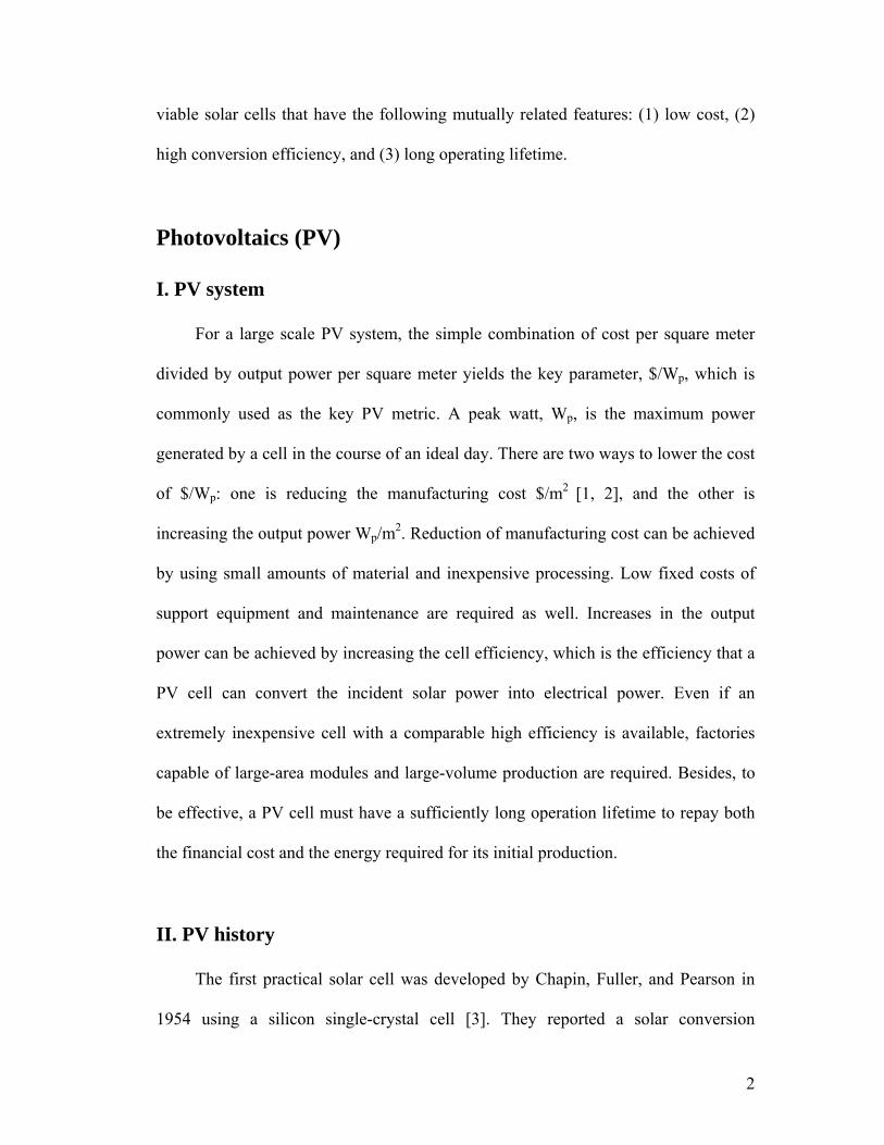
The current-voltage (J-V) behavior for an ideal solar cell is shown in Fig. 2.4(a).
When the applied voltage is zero, the current is called short-circuit current Jsc. For an
ideal solar cell, Jsc is equal to the photocurrent JL. When the total current is zero, the
voltage produced is the open-circuit voltage Voc. One can find the current and voltage
which deliver the maximum power to the load by setting the derivative of power
16
equal to zero, dP/dV = 0. Such current and voltage are referred to as the maximum-
power current Jmp and maximum-power voltage Vmp. Therefore, we can define a fill
factor FF by
ocsc
mpmp
VJVJ
FF = (2.13)
The conversion efficiency is given by
in
mpmp
PVJ
=η (2.14)
where Pin is the incident solar power on the solar cell.
Fig. 2.4: J-V characteristics of a p-n junction solar cell: (a) ideal dark and light J-V curves and (b) non-ideal J-V behavior with series resistance, shunt resistance, and a diode quality factor greater than 1.
However, for a non-ideal solar cell, the ideal J-V Eq. (2.12) must be modified
by including the series resistance Rs from ohmic loss, shunt resistance rsh from
17
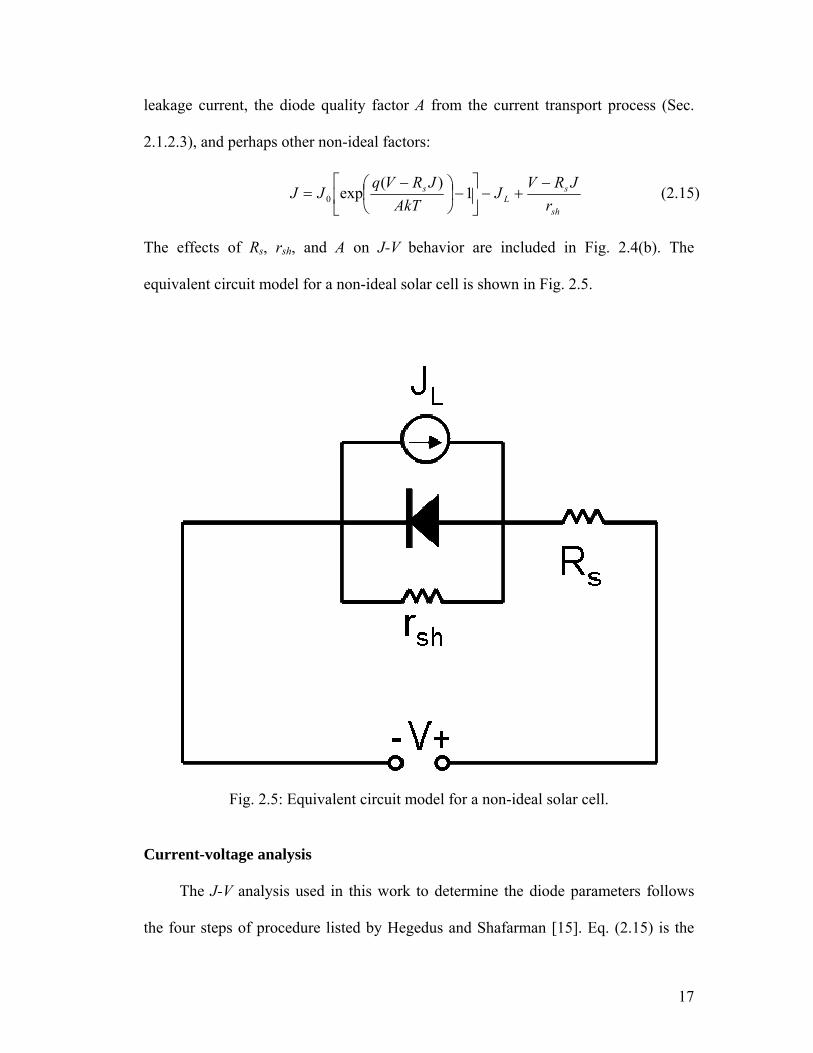
leakage current, the diode quality factor A from the current transport process (Sec.
2.1.2.3), and perhaps other non-ideal factors:
sh
sL
s
rJRV
JAkT
JRVqJJ
−+−⎥
⎦
⎤⎢⎣
⎡−⎟
⎠⎞
⎜⎝⎛ −
= 1)(
exp0 (2.15)
The effects of Rs, rsh, and A on J-V behavior are included in Fig. 2.4(b). The
equivalent circuit model for a non-ideal solar cell is shown in Fig. 2.5.
Fig. 2.5: Equivalent circuit model for a non-ideal solar cell.
Current-voltage analysis
The J-V analysis used in this work to determine the diode parameters follows
the four steps of procedure listed by Hegedus and Shafarman [15]. Eq. (2.15) is the

18
fundamental diode equation for this analysis procedure. The analysis process is
illustrated in Fig. 2.6(a) - (d).
Fig. 2.6: Four-step J-V analysis.
(a) The standard J-V curve. Jsc, Voc, FF and η can be derived from the J-V curve.
The next three plots are derived from this J-V curve.
(b) A plot of dJ/dV against V. If JL is constant, dJ/dV near Jsc and in reverse bias,
where the derivative of the diode term in Eq. (2.15) becomes negligible, will be flat

19
and the value in reverse bias equal to G = 1/rsh. There might be some noise
particularly under illumination.
(c) A plot of dV/dJ against (1 - dV/dJ * G) / (J + Jsc - GV). A linear fit to the
data gives an intercept of Rs and a slope of AkT/q, from which diode quality factor can
be calculated.
(d) A plot of J + Jsc - GV in a logarithmic scale against V - RsJ using the value of
Rs from plot (c). Then the intercept gives the value of J0, and the slope is q/AkT.
Therefore, A can be calculated and compared with the value from plot (c). For a well-
behaved polycrystalline solar cell, A is typically in the range 1.3 ≤ A ≤ 2, and the
values derived from plot (c) and (d) should agree well with each other.
2.1.2.3 Current transport mechanisms
In this section, the origin of the diode quality factor A will be discussed,
including why A is typically between 1 and 2. When one calculates the ideal-diode
equation (2.11), it is assumed that the electron and hole currents are constant
throughout the whole p-n junction. Then the total current is the sum of the minority-
electron diffusion current at the edge of the junction on the p-side and the minority-
hole diffusion current at the edge of the junction on the n-side. They can be written as
⎥⎦
⎤⎢⎣
⎡−⎟
⎠⎞
⎜⎝⎛= 1exp0
kTqV
LnqD
Jn
pnn (2.16)
⎥⎦
⎤⎢⎣
⎡−⎟
⎠⎞
⎜⎝⎛= 1exp0
kTqV
LpqD
Jp
npp (2.17)
where Dn and Dp are the electron and hole diffusion coefficients, np0 and pn0 are the
equilibrium electron concentration on the p-side and the equilibrium hole

20
concentration on the n-side respectively, and Ln and Lp are the electron and hole
diffusion lengths with τDL = , where τ is the lifetime. Then the reverse saturate
current J0 in the ideal-diode equation (2.11) is given by
p
np
n
pn
LpqD
LnqD
J 000 += (2.18)
Therefore the ideal-diode equation (2.11) calculates the diffusion current in a p-n
junction diode with a diode quality factor A equal to 1.
Under forward bias, the electrons and holes are injected across the space charge
region, and hence there are extra carriers in the space charge region. The possibility
exists that some of these electrons and holes will recombine within the space charge
region before they diffuse in the quasi-neutral region. The basic recombination
process can be the band-to-band recombination where an electron-hole pair
recombines, or more likely, it will be assisted by impurities. For the former process,
the transition of an electron from the conduction band to the valence band is possible
by emission of a photon (radiative process), or by transfer the energy to another free
electron or hole (Auger process). For the latter process, one or more trapping energy
levels are present in the bandgap, and the recombination can be described by electron
capture, electron emission, hole capture, and hole emission. The latter trap-assisted
recombination is generally referred to as Shockley-Read-Hall (SRH) recombination
[16, 17].
Under low injection conditions, that is, when the injected carriers are much less
than the majority carrier, the net SRH recombination rate for an n-type semiconductor
can be written as

21
p
pUτ∆
= (2.19)
and for a p-type semiconductor
n
nUτ∆
= (2.20)
where the minority-carrier lifetimes (hole lifetime τp in the n-type semiconductor and
electron lifetime τn in the p-type semiconductor) are
tthpp Nvσ
τ 1= (2.21)
and
tthnn Nvσ
τ 1= (2.22)
where σp and σn are the minority-hole and minority-electron capture cross sections, vth
is the carrier thermal velocity, and Nt is the trap density, which acts as the
recombination center for electrons and holes. The recombination rate approaches a
maximum as the energy level of the recombination center approaches midgap. Under
the assumption that the trap levels are located in the midgap and σp = σn = σ, the
recombination current in the space charge region under forward bias can be written as
⎟⎠⎞
⎜⎝⎛≈
kTqVnNvqWJ itthrec 2
exp2
σ (2.23)
where W is the width of the space charge region.
Then the total current in a p-n junction is the sum of the ideal diffusion current
and the recombination current:
)2
exp(2
)exp(0 kTqVnNvqW
kTqVJJJJ itthrecdiff σ+=+= (2.24)

22
The (-1) term in Eq. (2.11) is assumed to be negligible. In general, the diode current-
voltage relationship may be represented by
)exp(AkTqVJ ∝ (2.25)
The diode quality factor A is equal to 1 when the diffusion current dominates, and is
equal to 2 when the recombination is spatially uniform and the recombination current
dominates. When the currents are comparable, A has a value between 1 and 2.
2.2 Thin-film CdTe solar cells
Thin-film CdTe based solar cells are one of the most promising candidates for
photovoltaic energy conversion because of the great potential of low cost and high
efficiency. First, the cell is produced from polycrystalline materials and glass, which
are potentially much cheaper than bulk silicon. Second, the polycrystalline layers of a
CdTe solar cell can be deposited using a variety of different techniques [18], such as
close-space sublimation (CSS), which has been used to produce the highest efficiency
cells so far, chemical vapor deposition (CVD), and chemical bath deposition (CBD),
which is sometimes used for depositing CdS layer but not for high-efficiency CdTe
layer. Third, CdTe has a high absorption coefficient, so that approximately 99% of
the incident light is absorbed by a layer thickness of about 1µm. And finally, CdTe
has a band gap which is very close to the optimum bandgap for solar cells. Fig. 2.7
shows the ideal solar-cell efficiency at 300K under one-sun illumination as a function
of energy band gap. Note that the maximum value of ideal efficiency occurs near a
band gap of 1.5 eV, which is approximately the bandgap of CdTe. The corresponding
ideal efficiency for a CdTe solar cell is about 29%. Many factors will degrade the

23
ideal efficiency, so that efficiencies actually achieved should be lower. The record
laboratory efficiency for CdTe thin-film solar cell has reached 16.5% [7], and the
CdTe module performance is over 10% [19].
Fig. 2.7: Ideal solar-cell efficiency at 300 K for 1 sun. (Data reproduced from Sze [14].)
Fig. 2.7 also shows that GaAs crystalline solar cell with the comparable bandgap
(Eg = 1.42 eV) has the similar ideal efficiency about 29%. However, compared to the
16.5% record efficiency of CdTe thin-film solar cell, the laboratory efficiency for the
GaAs single-crystal solar cell is much higher around 26% to 27% [20]. This
difference is illustrated in Fig. 2.8. A modest mathematical modification was done to
adjust the GaAs bandgap to that of CdTe in Ref. [7], and hence the curve is labeled
“GaAs”. This adjustment increases the GaAs-cell voltage by 40 mV and decreases its

24
current density by 1 mA/cm2. There is a small current loss in CdTe cell, which has
been discussed in Ref. [21]. The largest contribution to the efficiency difference is the
voltage, where the value of the record CdTe cell is about 230 mV below the GaAs
cell. The analogous voltage difference for the other major thin-film polycrystalline
solar cell, Cu(In,Ga)Se2 (CIGS), is only about 30 mV when compared to crystalline
silicon. If the CdTe voltage deficit were reduced to the same 30 mV, with the same
current and fill-factor, CdTe cells would achieve the efficiency about 22%. The
reason for the relatively low voltage of CdTe solar cells is a combination of low
carrier density (~1014 cm-3) and low absorber lifetime (generally below 1 ns). In
practice, the voltage may be further compromised by the presence of a significant
back-contact barrier. The strategies for improving voltage and performance will be
explored and discussed in Chap. 4 and 5.
Fig. 2.8: Comparison of record CdTe cell with high-efficiency GaAs adjusted slightly for bandgap.

25
Fig. 2.9 shows the basic structure of the cross-section of a CdS/CdTe thin-film
solar cell, where the CdS layer and CdTe are deposited sequentially on a
glass/transparent-conducting-oxide (TCO) superstrate. It is called a superstrate
configuration.
Glass: transparent to the incident light. The outer face of the glass often has an
anti-reflective coat to enhance its optical properties.
TCO: an n+ transparent conductive oxide as a front contact with very high band
gap. It should have high optical transmittance and low resistivity. Usually the TCO
layer is made up of tin oxide (SnO2) or indium tin oxide (ITO). For low-temperature
CdS and CdTe deposition processes, ITO is the material of choice, and for CdS or
CdTe deposition requiring high temperature, SnO2 is the best material, since it is very
stable.
CdS: n-type layer as a part of the p-n heterojunction. The bandgap of CdS at
300K is 2.4 eV, which will absorb light in the short-wavelength region. CdS layer is
transparent for wavelengths above 520 nm, so it is often referred to as the window
layer. If the CdS is very thin (< 100 nm), much of the light with wavelengths below
520 nm will still pass through to the CdTe layer.
CdTe: p-type absorber layer with a high absorption coefficient. CdTe layer is
less highly doped than CdS layer, so the depletion region occurs mostly within the
CdTe. Therefore, CdTe is the active region of solar cell where most of carrier
generation and collection occur. The thickness of this layer is typically between 2 and
10 µm.
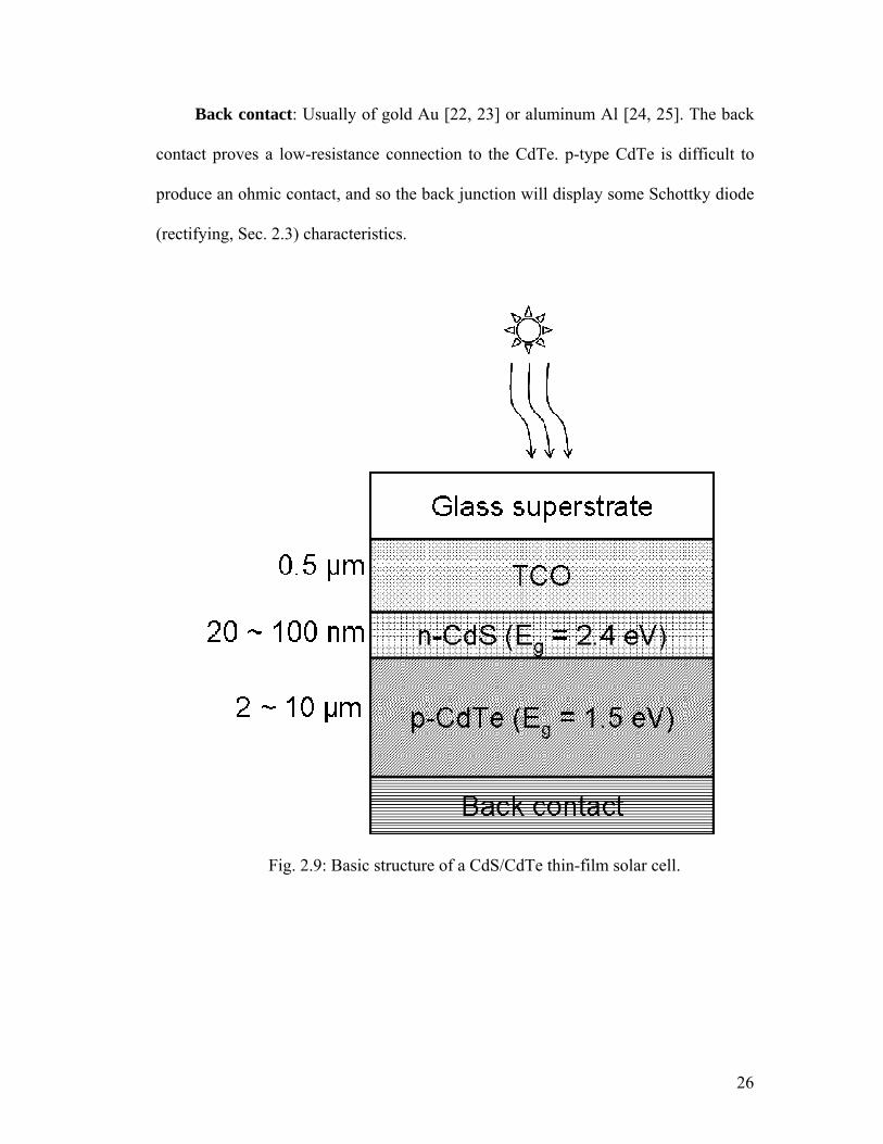
26
Back contact: Usually of gold Au [22, 23] or aluminum Al [24, 25]. The back
contact proves a low-resistance connection to the CdTe. p-type CdTe is difficult to
produce an ohmic contact, and so the back junction will display some Schottky diode
(rectifying, Sec. 2.3) characteristics.
Fig. 2.9: Basic structure of a CdS/CdTe thin-film solar cell.

27
2.3 Back contact of CdTe solar cells
When a metal contacts a semiconductor, the Fermi-level in the two materials
must line up so that the charge will flow from the semiconductor to the metal and
thermal equilibrium will be established. In general, the contact between metal and
semiconductor can be ohmic or rectifying (Schottky contact). An ohmic contact
should have a relative negligible contact resistance compared to the bulk
semiconductor, and it should not significantly perturb the device performance. A
Schottky contact, however, will be an obstacle for the charge carriers in the
semiconductor, and thus influence the device performance.
Both a p-type semiconductor/metal ohmic contact and a Schottky contact are
shown in Fig. 2.10. The electron affinity χ in semiconductor is measured from the
bottom of the conduction band to the vacuum level, and the work function φm is
defined as the energy difference between the vacuum level and the Fermi level of the
metal. An ohmic p-type semiconductor/metal contact is formed when
χφ +≥ gm E (2.26)
and a Schottky contact is formed when
χφ +< gm E (2.27)
The ohmic contact provides conduction between the semiconductor and the metal,
since there is no barrier for electrons and holes at the semiconductor/metal interface.
However, for the Schottky contact case, the majority-carrier holes meet a barrier
when they travel from the semiconductor to the metal. The contact-barrier height for
holes at the semiconductor/metal interface is given by the difference between the
edge of the valence band and the Fermi level in the metal:

28
mgb E φχφ −+= (2.28)
Fig. 2.10: p-semiconductor/metal ohmic contact and rectifying (Schottky) contact.
p-type CdTe has a high electron affinity χ = 4.5 eV, and a band gap Eg = 1.5 eV.
Therefore, a metal with a high work function φm ≥ 6.0 eV is required to make an
ohmic contact, which corresponds to a negative or zero back-contact barrier. In
practice, a back-contact barrier of 0.3 eV or lower is sufficient to effectively be an
ohmic contact. Most metals do not have sufficiently high work functions, and
therefore Schottky back contacts are generally present in CdTe solar cells. Table 2.1
lists the work functions of Ag, Al, Au and Cu, and the resulting back-contact barriers
for holes when these metals are deposited to CdTe layer.

29
Table 2.1: Metal work functions φm and resulting back-contact barriers φb in CdTe.
Metal Work function φm [eV] Back barrier φb [eV] Ag 4.26 1.74 Al 4.28 1.72 Au 5.1 0.9 Cu 4.65 1.35
The presence of a Schottky back contact in CdTe solar cell can significantly
affect the cell performance by limit the hole current flow, especially at operating
voltages and above. The results is that the J-V curve of a CdTe solar cell exhibits a
reduced FF blow Voc, and a limited forward current above Voc (referred to as rollover)
[26 – 28]. This mechanism can be approximated using circuit model (shown in Fig.
2.11) that places the main diode in series with a reverse back-contact diode. Fig. 2.12
shows the experimental J-V data and the simulated J-V curve of a typical CdTe cell
with rollover. (This work was done by S. Demtsu [29].) The parameters extracted
from the experimental data are J0 = 7x10⁻⁴ mA/cm2, JL = 24 mA/cm2, A = 2.9, Rs = 1.4
Ω-cm2, rsh = 1500 Ω-cm2. For this cell, the height of the back-contact barrier is 0.55
eV, which is much lower than the values shown in Table 2.1. Using these parameters
and a back diode shunt resistance of rbsh = 75 Ω-cm2, the J-V characteristic can be
simulated analytically. In practice, better performance of J-V curves can be achieved
with the inclusion of Cu in the back contact [30].
The accuracy of two-diode approach, however, is limited, because the
assumption that the two diodes do not interact does not hold in many cases. The flow
of minority-carrier electrons from the front diode to the back diode can cause a
substantial change in the device behavior and can help explain the experimentally
observed characteristics. We will discuss this in detail in Chap. 5.

30
Fig. 2.11: Equivalent circuit model of a main diode in series with a reversed back diode.
Fig. 2.12: Experiment J-V data and the simulated J-V curve of a typical CdTe solar cell with rollover. (Data reproduced from Demstu [29].)

31
Chapter 3
Numerical Simulations
3.1 Modeling
In general, any numerical program which can solve the basic semiconductor
equations can be used to simulate the thin-film solar cells. These basic semiconductor
equations are Poisson’s equation, the continuity equation for free electrons, and the
continuity equation for free holes. The physics of device transport can be achieved by
solving these three governing equations along with the appropriate boundary
conditions.
3.1.1 Poisson’s equation
Poisson’s equation relates the electric field E to the charge density. In one-
dimension space, Poisson’s equation is given by
ερ
=dxdE (3.1)
where ε is the permittivity [14]. Since the electric field E can be defined as –dΨ/dx,
where Ψ is the electrostatic potential, and the charge density ρ can be expressed by

32
the sum of free electron n, free hole p, ionized donor doping +DN , ionized acceptor
doping −AN , trapped electron nt, and trapped hole pt, Poisson’s equation can be written
as
( ))()()()()()()( xnxpxNxNxnxpqdxdx
dxd
ttAD −+−+−=⎟⎠⎞
⎜⎝⎛ Ψ− −+ε (3.2)
Free-electron density n(x) and free-hole density p(x) can be expressed by Fermi
level EF through Eq. (2.3) and (2.4) in thermal equilibrium. If a device is not in
thermal equilibrium, such as when it has an applied voltage bias, a light bias, or both,
the quantities n(x) and p(x) can be expressed by electron quasi-Fermi level EFn and
hole quasi-Fermi level EFp respectively through Eq. (2.9) and (2.10).
+DN and −
AN are the charge densities arising from the localized shallow doping
levels. These shallow doping levels are often purposefully present through intentional
introduction of impurities. The quantities of +DN and −
AN can also be expressed by
Fermi level EF in thermal equilibrium, or quasi-Fermi levels EFn and EFp under bias.
Trapped-electron density nt and trapped-hole density pt are determined from the
defect states which are inadvertently present. These defect states can be donor-like or
acceptor-like. The density of charged acceptor-like defect states is referred to as
trapped-electron density nt, and that of charged donor-like defect states as trapped-
hole density pt. Similar as the shallow doping levels, charged defect levels, nt and pt,
can still be calculated by Fermi level or quasi-Fermi levels.
3.1.2 Continuity equations
33
More information about free electrons and free holes is needed to determine
how they change across a device and under different biases. The equations that keep
track of changes in the conduction-band electrons and valence-band holes are the
continuity equations, which are given by [14]
→
•∇+−=∂∂
nnn Jq
UGtn 1 (3.3)
→
•∇−−=∂∂
ppp Jq
UGtp 1 (3.4)
where Gn and Gp are the electron and hole generation rates, which are result from a
external influence such as optical excitation. We assume that the device is in steady
state, which means the time rate of the change of free carriers is equal to zero. Then
in one-dimension space, the continuity equation for free electrons is given by
)()())(
(1 xUxGdx
xdJq nn
n +−= (3.5)
and the continuity equation for free holes is given by
)()())(
(1 xUxGdx
xdJq pp
p −= (3.6)
The electron current density Jn and hole current density Jp consist of the drift
component caused by the electric field and the diffusion component caused by the
gradient of the carrier concentration. For a one-dimension case, they are given by
dxdnqDnEqxJ nnn += µ)( (3.7)
dxdpqDpEqxJ ppp −= µ)( (3.8)
34
where µn and µp are the electron and hole mobility respectively, and Dn and Dp are the
electron and hole diffusion coefficient respectively, which are approximated by the
Einstein relationship in the low-density limits
nn qkTD µ= (3.9)
pp qkTD µ= (3.10)
Therefore, Eq. (3.7) and (3.8) can be written as
dxdE
ndxdn
qkTnEqxJ Fn
nnn µµ =+= )()( (3.11)
dxdE
pdxdp
qkTpEqxJ Fp
ppp µµ =−= )()( (3.12)
We assume that the electron and hole generation rates Gn(x) and Gp(x) are due
to the external illumination, and hence Gn(x) and Gp(x) are optical generation rates.
When a device is illuminated by a light source with a photon flux of Φ (hν ≥ Eg), the
photon flux enters the device, and the generation rate of electron-hole pairs in the
device is proportional to the spatial rate at which the photon flux decreases. Therefore,
the optical generation rate is given by
dxxdxG )()( Φ
−= (3.13)
and the photon flux Φ(x) by
( )xx α−Φ=Φ exp)( 0 (3.14)
Thus, Eq. (3.13) can be written as
)exp()( 0 xxG αα −Φ= (3.15)
35
where α is the absorption coefficient of the semiconductor material for the
wavelength used.
The recombination process in the device has been discussed in Sec. 2.1.2.3. The
net recombination rate in the device includes both the band-to-band recombination
(direct recombination), and the SRH recombination through the defect states (indirect
recombination).
3.1.3 Boundary conditions
The three governing equations should be solved in each position of a device.
The solutions to these three equations are the electrostatic potential Ψ(x), the electron
quasi-Fermi level EFn(x), and the hole quasi-Fermi level EFp(x), or equivalently Ψ(x),
n(x) and p(x). They should be defined at every position x, and hence the total system
can be defined and the transport characteristics can be determined. However, since
these three equations are non-linear differential and coupled, they cannot in general
be solved analytically. Therefore, numerical methods are often utilized to numerically
solve the three equations, and the boundary conditions have to be imposed in the
equations.
Assuming the device length is L, there are three sets of boundary conditions.
The first set is the electrostatic potential Ψ evaluated at x = 0 and x = L. The other
two sets of boundary conditions are the electron current density Jn and hole current
density Jp evaluated at x = 0 and x = L. Both Jn and Jp boundary conditions depend on
the surface recombination speed and the change of the carrier population at x = 0 and
x = L. Also, they must be matched by the continuity equations. All of the three sets of

36
boundary conditions should be valid for all structures for all situations whether in
thermal equilibrium or under light or voltage bias.
3.1.4 Solution technique
To numerically solve the three non-linear, coupled governing equations, the
one-dimension device with length L is divided into N intervals and N + 1 major grid
points, shown as in Fig. 3.1. The grid spacing need not be uniform. The Poisson’s
equation and the continuity equations will be solved for each interval along with the
appropriate boundary conditions, and the set of three variables Ψ, EFn, and EFp are
then solved at each particular grid point 1 to N + 1, represented by solid lines. Once
the variables Ψ, EFn, and EFp are determined under the light, voltage, and temperature
conditions, and other variables such as electric field, carrier concentration, or trapped
charges are defined, the recombination profiles, electron and hole current densities,
and other transport information may be obtained. Then the total J-V characteristic can
be obtained from J(x) = Jn(x) + Jp(x).
Fig. 3.1: Intervals and grids used in numerical method. There are N intervals (dashed lines) and N + 1 major grid points (solid lines).
3.2 Software

37
Numerical simulation of a solar cell is an important way to predict the effect of
physical changes on cell performance and to test the viability of the proposed
physical explanation. Several numerical programs have been developed and widely
used recently. In this dissertation, two software packages are utilized to simulate the
thin-film CdS/CdTe solar cells. One is AMPS software and another is SCAPS
software. Both are one-dimension device simulation programs.
3.2.1 AMPS-1D
AMPS-1D is a one-dimension device simulation program for the Analysis of
Microelectronic and Photonic Structures. It was developed by Prof. S. J. Fonash et al.
in the Electronic Materials and Processing Research Laboratory at Pennsylvania State
University. BETA version 1.0, which was revised in 1997, is used here. It can analyze
the transport in a variety of crystalline, polycrystalline, or amorphous solar-cell
materials, and device structures including homojunction, heterojunction, or multi-
junction solar cells and detectors [31 – 34].
The AMPS-1D program asks the user to input the specific parameters to build
the structure to be tested. When running the AMPS simulation, the program expects a
set of default parameters. The user can save the default case as the case name he/she
prefers and reset the parameters to be varied for a particular configuration. The
advantages of AMPS include its user friendliness and the stability in general. It also
has a very flexible plotting program, in which the user can generate output plots such
as J-V curves, spectral response, band diagrams, carrier concentrations and currents,
and recombination profiles under various bias conditions. This package allows the

38
user to explore the physical transport of the device directly. However, AMPS has
some disadvantages, such as the need to input all information including spectrum
parameters by hand and the lack of interface treatment so that an interface must be
approximated by thin layers.
3.2.2 SCAPS-1D
SCAPS-1D is a Solar cell Capacitance Simulator in one dimension. It is
developed by Prof. M. Burgelman et al. in the Department of Electronics and
Information Systems at University of Gent, Belgium. Version 2.4 used here was
developed in 2003. This program has been developed to realistically simulate the
electrical characteristics (dc or ac) of thin-film heterojunction solar cells. It has been
tested for thin-film CdTe and CIGS solar cells [35 – 39].
SCAPS is able to simulate standard characteristics such as current-voltage
curves and spectral response, as well as advanced measurements like capacitance-
voltage and capacitance-frequency relationships. It is also possible to specify the
external series resistance Rs. The other advantages include: all input files are text file
including the spectrum parameters and device definition files; the ability to have
abrupt interfaces; high speed; and when convergence fails, the points already
calculated are not lost. The disadvantages of SCAPS are that it can be unstable; all
model calculations need to be performed by hand in the action panel; and the plotting
interface is not friendly.
3.3 Baseline parameters
39
A three-layer device model of a SnO2/CdS/CdTe solar cell is the starting point
for the calculations in this dissertation. A baseline case [40] was discussed and
designed to approximate the highest-efficiency CdTe solar cells at that time [7], and it
is slightly modified in this dissertation. The material parameters of baseline case are
listed in Table 3.1, where S is the surface recombination velocity, d is the layer
thickness, ∆EC is the conduction band offset, NDG(AG) is the donor-like (acceptor-like)
defect density, ED(A) is the peak energy of defect state, and WG is the energy
distribution width of defect state. The other symbols in Table 3.1 have their usual
definitions.
Table 3.1: SnO2/CdS/CdTe solar cell baseline parameters.
General Device Properties Front Back
Barrier Height [eV] 0.1 (EC-EF) 0.3 (EF-EV) Sn [cm/s] 107 107 Sp [cm/s] 107 107
Reflectivity [1] 0.1 0.8 Layer Properties
SnO2 CdS CdTe d [nm] 500 25 4000 ε/ε0 [1] 9 10 9.4
µn [cm2/Vs] 100 100 320 µp [cm2/Vs] 25 25 40
NA, ND [cm-3] ND: 1017 ND: 1.1×10¹⁸ NA: 2×10¹⁴ Eg [eV] 3.6 2.4 1.5
NC [cm-3] 2.2×10¹⁸ 2.2×10¹⁸ 7.8×10¹⁷ NV [cm-3] 1.8×10¹⁹ 1.8×10¹⁹ 1.8×10¹⁹ ∆EC [eV] 0 -0.1
Gaussian (midgap) Defect States SnO2 CdS CdTe
NDG, NAG [cm-3] D: 1015 A: 1018 D: 2×10¹³ ED, EA [eV] midgap midgap midgap
WG [eV] 0.1 0.1 0.1 σn [cm2] 10-12 10-17 10-11 σp [cm2] 10-15 10-12 10-14

40
The optical absorption spectra are based on experimental results for
polycrystalline CdS and CdTe films [41], and a standard terrestrial illumination
spectrum is assumed [42]. SnO2 is used for the transparent conducting oxide. The
conduction bands at the SnO2/CdS interface are assumed to be aligned with ∆EC = 0,
since there appears to be no experimental evidence of a detrimental offset there. The
CdS layer is assumed to be compensated, but sufficiently photoconductive that its
detailed properties have little effect on the illuminated-cell-transport. Most
experimental and theoretical results show that the ∆EC at CdS/CdTe interface is
between zero to -0.3 eV. ∆EC = -0.1 eV, consistent with theoretical results [43], is
used. The baseline CdTe hole density is taken to be 2 × 1014 cm-3, and the baseline
deep-donor-level defect density is chosen to be 2 × 1013 cm-3 (Ref. [40] used 2 × 10¹⁴
cm-3 for both hole density and defect density). Although the defect density and
capture cross sections are independently specified, the resulting lifetimes for electrons
and holes, which are calculated from Eq. (2.21) and (2.22), are the key parameters.
The model parameters are chosen such that the SRH electron lifetime in the quasi-
neutral bulk region of the p-type CdTe absorber is 0.5 ns, and the resulting carrier
diffusion length of 0.6 µm is substantially shorter than the CdTe thickness (4 µm).
The baseline hole lifetime is taken to be three order of magnitude larger than that of
the electrons, because unlike for electrons, there is no electrostatic attraction between
the assumed donor-like defects and holes. In Chap. 4 and Chap. 5, we will discuss the
effects of the lifetime variation, when lifetimes are varied, but the τn/τp ratio is held
constant. The back-contact-barrier height φb = 0.3 eV is used as baseline, because this
value yields flat conduction and valence bands at the back contact. The band diagram

41
of the baseline case at zero bias under illumination is shown in Fig. 3.2. Low CdTe
hole density around 2 × 1014 cm-3 is typical of today’s cells and makes the CdTe
absorber intermediate between i-type (intrinsic) and p-type. As a consequence, the
depletion region extends over a large fraction, but not all, of the CdTe thickness.
Fig. 3.2: Conduction and valence bands and quasi-Fermi levels for the baseline case under illumination at zero bias.
Fig. 3.3 shows the dark/light J-V curves for the baseline case. With the 0.3-eV
back-contact barrier, the baseline Voc is slightly higher than that in Ref. [40]. The
solar-cell performance parameters for the baseline case are open-circuit voltage Voc =
0.89 V, short-circuit current density Jsc = 24.5 mA/cm2, fill factor FF = 79.5%, and
efficiency η = 17.3%. The diode quality factor A, determined from J-V analysis, is
approximately 1.7.

42
Fig. 3.3: Dark and light J-V curves for the baseline case.

43
Chapter 4
Impact of CdTe Carrier Lifetime Without
a Secondary Barrier
4.1 Effect of carrier lifetime with typical carrier density
The minority-carrier lifetime of the CdTe solar cells from time-resolved
photoluminescence has been reported [44 – 46], and the resulting lifetimes for typical
CdTe solar cells have ranged from 0.1 ns to 2 ns. To examine the impact of the CdTe
carrier lifetime on current-voltage curves, the numerical modeling methods, AMPS-
1D and SCAPS-1D, were used to simulate the effects. The baseline configuration
assigned a typical carrier density of 2 × 1014 cm-3, a lifetime of 0.5 ns, and a small
back-contact barrier φb = 0.3 eV. A 4-µm CdTe thickness was used in all the
simulations. Different thicknesses will alter the details, but in general not the form or
the magnitude of the results. The J-V curve was calculated as a function of the CdTe
recombination lifetime τ with the ratio of τn to τp held constant.
44
4.1.1 Space-charge-region recombination
First, the electron and hole lifetimes in CdTe layer were decreased by a factor
of 10 from the baseline case. The resulting CdTe minority-electron lifetime is 0.05 ns.
The calculated dark and light J-V curves with the lower lifetime and the baseline
reference (BL) are shown in Fig. 4.1. Without a significant back barrier, shorter
lifetime results in more recombination in the space-charge region and, therefore, a
higher forward current that leads to a lower Voc and fill factor. Space-charge-region
recombination with a diode quality factor of approximately 2 is assumed, which
corresponds to recombination centers deep in the band gap.
Fig. 4.1: Dark and light J-V curves with lifetimes decreased by a factor of 10 from the baseline (BL) case. Dashed line represents the light BL case.
4.1.2 Dominant electron current

45
Fig. 4.2 shows the calculated J-V curves when the electron and hole lifetimes
in CdTe layer are increased by a factor of 10 from the BL case, resulting in a CdTe
minority-electron lifetime of 5 ns. Longer CdTe lifetime will both reduce the forward
current due to lower SCR recombination and increase the forward flow of electrons to
the back contact. The net result, shown in Fig. 4.2, is a significant increase in fill
factor, with A approaching 1, but little effect on voltage.
Fig. 4.2: Dark and light J-V curves with lifetimes increased by a factor of 10 from the baseline (BL) case. Dashed line represents the light BL case.
Longer lifetime allows higher injection of minority carriers into the quasi-
neutral region where they recombine or, more likely, diffuse to the back-contact and
then recombine. This current is associated with a diode quality factor of 1, since the
recombination rate only depends on the electron density n. The diode quality factor
46
determined from the simulated long-lifetime J-V curve is about 1.2. Slightly higher
Voc is achieved, but the major improvement compared to the BL case is in the FF.
This is an indicator that the BL case with its diffusion length of 0.6 µm is already
relatively strongly influenced by the back-contact current. A substantial electron
current toward the back-contact must be expected, because the wide depletion width
(W) substantially narrows the quasi-neutral region and the relatively low doping
allows for higher minority-carrier injection levels at the edge of the main junction
depletion region.
Following the conventional presentation [14], the contrast between Fig. 4.1
and 4.2 can be illustrated by logarithmic plots of current vs. voltage as shown in Fig.
4.3. With moderate or short lifetime (solid lines), Voc is limited by SRH
recombination with a solid crossover above Jsc, and hence the diode quality factor is
about 2. This is generally assumed to be the case for CdTe solar cells. If the lifetime
is substantially increased (dashed lines), SCR recombination is reduced and the
bulk/back-contact recombination current is increased. In this situation, the crossover
of dashed lines occurs below Jsc, and the back-contact recombination with a diode
quality factor of approximately 1, will determine the open-circuit voltage. In this case,
Voc will change very little with the CdTe lifetime.

47
Fig. 4.3: Forward currents in p-n junctions due to Shockley-Read-Hall recombination through midgap states (A = 2) and recombination in the bulk region or at the back-contact (A = 1). Depending on the carrier lifetime, Voc is limited by one or the other.
4.1.3 Carrier-lifetime variations
A series of calculated light J-V curves for absorber lifetimes that span a range
somewhat larger than the 0.1 to 2 ns typical of current cells are shown in Fig. 4.4. The
CdTe electron lifetime is varied from 0.005 ns to 50 ns. The hole lifetime is in each
case taken to be 1000 times greater than the electron lifetime. The center J-V curve
corresponds to the BL case with electron lifetime of 0.5 ns, and the light J-V curves
for Fig. 4.1 and 4.2 correspond to two of the other curves. The “GaAs” curve, which
was shown in Fig. 2.8, is repeated here for reference. Increasing lifetime leads to

48
increasing fill-factor and increasing voltage up to a point. Physically, this
corresponds to a smaller number of recombination defect states.
Fig. 4.4: Simulated J-V curves for typical-carrier-density CdTe with varying lifetime.
Fig. 4.5 shows the calculated Voc and fill-factor as a function of CdTe electron
lifetime. For large lifetimes, the fill-factor approaches that of GaAs and corresponds
to a diode quality factor close to unity. The voltage, however, increases when the
lifetime is small, but then saturates at a value well below that of “GaAs”, in fact only
slightly above values of Voc that have been achieved experimentally. Hence,
increasing lifetime alone will not significantly raise the CdTe solar-cell voltage above
current values.

49
Fig. 4.5: Calculated Voc and fill-factor for typical-carrier-density CdTe as a function of lifetime.
The calculated diode quality factor A as a function of CdTe electron lifetime is
shown in Fig. 4.6. In the dark, A approaches 2 at low lifetime due to SRH
recombination, and approaches 1 at high lifetime due to high diffusion. Under
illumination, however, the values of A are artificially higher than that in the dark,
especially in the low lifetime region where the apparent value of A can be greater than
2. This is because the J-V analysis process Fig. 2.6(c) and (d) assumes a constant light
current JL with the magnitude equal to Jsc, however, when the lifetime is low, JL is no
longer constant but voltage dependent, and under such conditions, standard analysis
procedures do not yield the appropriate value of A.

50
Fig. 4.6: Calculated diode quality factor A for typical-carrier-density CdTe as a function lifetime.
The difference between the high and low lifetime regimes is well illustrated by
plotting dJ/dV vs. V as a function of lifetime, as shown in Fig. 4.7. If JL is constant,
dJ/dV near zero bias and in reverse bias will be constant with a value equal to G =
1/rsh. Fig. 4.7, however, shows that JL is not constant but voltage dependent when the
lifetime is low. As the lifetime is increased, JL becomes less voltage dependent, and in
the high lifetime region, it will be constant. Therefore, with moderate or high lifetime,
the calculation of diode quality factor A will be more reliable.
The reductions in fill factor shown in Fig. 4.5 can be attributed to a voltage-
dependent JL, and therefore a voltage-dependent collection efficiency. Ideally, a light
J-V curve is the dark curve shifted by the collected photocurrent, and the collection
efficiency CE can be defined as

51
0
)()(
L
DarkLight
JVJVJ
CE−
= (4.1)
where JL0 is the light-generated current [47, 48]. A similar expression, which
evaluates J-V curves at different intensities addresses possible changes to the band
structure induced by illumination [47], but assumes that the structure in the light is
independent of intensity. We have advocated caution in attributing dark/light non-
superposition to collection efficiency [48], especially when there is an obvious
crossover of light and dark curves and a likely influence of secondary front or back
barriers.
Fig. 4.7: dJ/dV vs. V for typical-carrier-density CdTe and different lifetime.
With a typical CdTe carrier density and the absence of a significant back barrier,
the dark J-V curves in the electron-lifetime range of 0.005 ns to 50 ns are well

52
behaved, and the light and dark J-V curves (Fig. 4.1 and Fig. 4.2) do not show
obvious crossover. Therefore the conventional evaluation of collection efficiency
works, at least for voltages not significantly above Voc. Collection-efficiency curves
deduced from Eq. (4.1) for various lifetimes are shown in Fig. 4.8. As the electron
lifetime is reduced, one clearly sees a significant decrease in collection efficiency as
the voltage approaches Voc. This accounts for the lower fill factors observed when
carrier lifetimes is small.
Fig. 4.8: Collection efficiency for typical-carrier-density CdTe with varying lifetime. Also shown for reference is Voc for each lifetime.
4.2 Effect of carrier lifetime with high carrier density
Fig. 4.9, where the CdTe hole density is increased by three orders of magnitude
to 2 × 1017 cm-3, is the classic n-p hetero-junction. With significantly high carrier

53
density, the depletion width will be much shorter than that in the BL case (Fig 3.2). It
is in fact very similar to what one would find with n-on-p GaAs, and we will explore
what might be altered with polycrystalline CdTe to achieve performance comparable
to GaAs.
Fig. 4.9: Conduction and valence bands and quasi-Fermi levels for high-carrier-density CdTe under illumination at zero bias.
Fig. 4.10 shows the simulated J-V results for various carrier lifetimes when the
CdTe hole density is increased to 2 × 1017 cm-3. The “GaAs” curve is still repeated
here for reference. The calculated Voc and fill-factor as a function of CdTe electron
lifetime are shown in Fig. 4.11. In this case, the voltage, as well as the fill factor,
approaches the “GaAs” values at the higher lifetimes. Another effect that becomes
more important at higher-carrier densities is the dependence of current density on

54
lifetime. This dependence results from the narrow depletion thickness at higher
carrier density relative to optical absorption depth. A narrow depletion and a low
lifetime lead to a small photocurrent collection and therefore, compared with typical
carrier density of 2 × 1014 cm-3 (Fig. 4.5), a photocurrent is significantly reduced with
narrow depletion. A large diffusion length, and hence a high lifetime, becomes
essential for reasonable collection of photo-generated electrons.
Fig. 4.10: Simulated J-V curves for high-carrier-density CdTe with varying lifetime.

55
Fig. 4.11: Calculated Voc and fill-factor for high-carrier-density CdTe as a function of lifetime.
4.3 Combination of carrier-lifetime and carrier-density
variations
Fig. 4.12 summarizes the combined effects of lifetime and carrier density on the
voltage. The carrier density is varied from 2 × 1014 cm-3 to 2 × 1017 cm-3. Fig. 4.12
shows graphically that both high lifetime and high carrier density are required for
high voltage in the n-p configuration. Physically, a reduction in the density of defects
is the likely key to both: increased lifetime though a smaller number of recombination
centers and increased carrier density through a smaller number of compensating states.
One risk, however, is that CdS/CdTe is a heterojunction with the potential for

56
interfacial recombination, which can become the voltage-limiting factor when the
bulk CdTe properties are significantly improved.
Fig. 4.12: Calculated Voc as a function of lifetime and carrier density.
4.4 Effect of CdS/CdTe interfacial recombination and
conduction-band offset
Interfacial recombination can be reasonably parameterized by an interfacial
recombination velocity vintf, but the J-V impact of such recombination is also strongly
affected by the magnitude of the CdS/CdTe conduction-band offset ∆Ec [49]. For
CdTe, ∆Ec has been shown experimentally [50] and theoretically [43] to be close to
zero and is probably slightly negative, the direction often referred to as a “cliff”.
Earlier work, which was focused on CIGS, showed that such a cliff, or a small

57
“spike” (∆Ec < +0.1 eV), can limit the ability of voltage to increase with band gap
even when vintf is several orders on magnitude less than the thermal velocity vth [49].
The conclusion was that it is important to engineer ∆Ec to produce a spike in the 0.1-
to 0.4-eV range.
Figure 4.13(a), for typical hole density (2 × 1014 cm-3) and large lifetime (τn = 10
ns), shows the calculated CdTe voltage as a function of ∆Ec, physically implying that
one might use an alternative window layer or alloy CdTe to reduce its band gap. The
four curves correspond to different values of vintf, and it is clear that even a very small
amount of interfacial recombination will severely limit Voc for a large cliff. At the
presumed value of ∆Ec equal to -0.1 eV, however, the effect on typical-density CdTe
cells is quite modest.
For higher hole density (2 × 1017 cm-3), as shown in figure 4.13(b), the voltage
with vintf = 0 is larger, but the voltage loss when vintf ≠ 0 can be very much larger and
at least partially negates the voltage gain from the carrier-density increase. Hence, an
alternative window or CdTe alloy is likely to be much more critical, even with small
vintf. The details, however, will depend on how the CdS and CdTe doping densities
affect the Fermi level at the interface. Fig 4.13(a) and (b) show that although the
CdS/CdTe conduction-band offset is not a significant voltage limitation at present, it
will very likely become more of an issue if carrier density and voltage are increased.

58
Fig. 4.13: Dependence of Voc on CdS/CdTe band offset and interfacial recombination for (a) typical-carrier-density CdTe, (b) high-carrier-density CdTe.

59
Chapter 5
Impact of CdTe Carrier Lifetime and
Secondary Back Barrier
5.1 Possible secondary back barrier for CdTe solar cells
Typical CdTe solar cells include an n+-type transparent conducting oxide, an n-
type buffer layer (typically CdS), 2–10 µm of p-CdTe, and a metal back-contact. As
mentioned in Chapter 2, since most metals do not have sufficiently high work
functions, it is difficult to produce an ohmic contact to p-type CdTe which would
require a back-contact barrier of 0.3 eV or lower. The CdTe/metal contact often forms
a blocking Schottky barrier that can limit the flow of holes and cause a substantial
change in the device performance.
It is also possible in principle to have a conduction-band barrier at the back of
the CdTe absorber which keeps the minority carriers away from the CdTe/metal
interface. This possible back barrier is referred to as a back electron reflector and
could reduce or eliminate recombination at the back contact. One possibility for

60
creating such a barrier is to add a layer of ZnTe [51] or other material with an
expanded gap in the conduction-band direction.
Since the back hole barrier is a critical issue for CdTe solar cells, the
following sections will evaluate CdTe solar cells with such a blocking barrier and a
large range of electron lifetimes. The details will be evaluated by numerical
simulations in one dimension, and the effect of a back electron reflector for voltage
performance will be evaluated briefly.
5.2 Effect of carrier lifetime with back hole barrier
In p-type CdTe material, the absorber thickness (d) is typically substantially
greater than the minority carrier diffusion length (Ln), and it is therefore commonly
assumed that minority electron currents at the back-contact are negligible. Despite the
apparent contradiction with Ln/d << 1, Niemegeers and Burgelman [27] showed that
in some cases non-negligible electron current can explain crossover of light and dark
J-V curves. Beier et al. [52] and Burgelman et al. [53] continued the development of
this approach and discussed several mechanisms that can lead to a voltage
dependence of the back-contact saturation current. Our results explicitly demonstrate
that minority-electron currents are significant even with Ln/d ~ 0.1. In fact, they can
substantially limit the device performance.
The combined effects of a significant back-contact barrier and a typical absorber
carrier density frequently alter the current-voltage (J-V) characteristics of CdTe solar
cells. This combination leads to two competing mechanisms that can alter the J-V
characteristics in two different ways. One is a majority-carrier (hole) limitation on
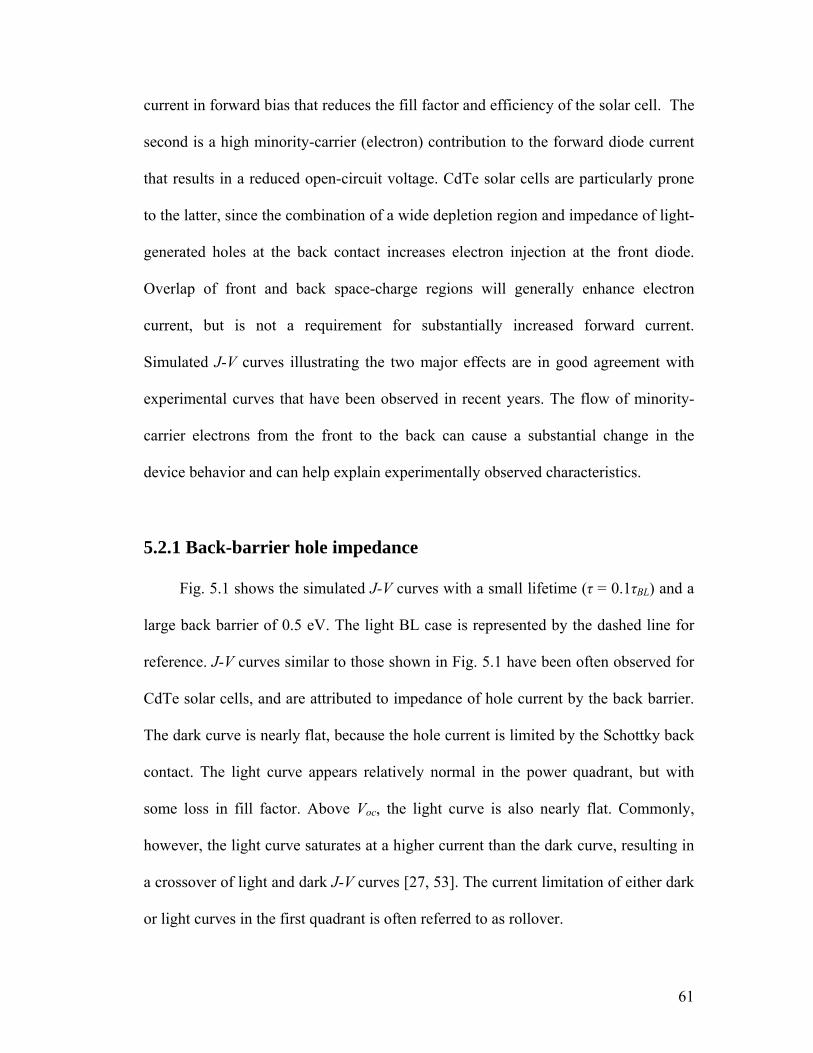
61
current in forward bias that reduces the fill factor and efficiency of the solar cell. The
second is a high minority-carrier (electron) contribution to the forward diode current
that results in a reduced open-circuit voltage. CdTe solar cells are particularly prone
to the latter, since the combination of a wide depletion region and impedance of light-
generated holes at the back contact increases electron injection at the front diode.
Overlap of front and back space-charge regions will generally enhance electron
current, but is not a requirement for substantially increased forward current.
Simulated J-V curves illustrating the two major effects are in good agreement with
experimental curves that have been observed in recent years. The flow of minority-
carrier electrons from the front to the back can cause a substantial change in the
device behavior and can help explain experimentally observed characteristics.
5.2.1 Back-barrier hole impedance
Fig. 5.1 shows the simulated J-V curves with a small lifetime (τ = 0.1τBL) and a
large back barrier of 0.5 eV. The light BL case is represented by the dashed line for
reference. J-V curves similar to those shown in Fig. 5.1 have been often observed for
CdTe solar cells, and are attributed to impedance of hole current by the back barrier.
The dark curve is nearly flat, because the hole current is limited by the Schottky back
contact. The light curve appears relatively normal in the power quadrant, but with
some loss in fill factor. Above Voc, the light curve is also nearly flat. Commonly,
however, the light curve saturates at a higher current than the dark curve, resulting in
a crossover of light and dark J-V curves [27, 53]. The current limitation of either dark
or light curves in the first quadrant is often referred to as rollover.

62
Fig. 5.1: Calculated dark and light J-V curves with lifetimes decreased by a factor of 10 from the baseline (BL) case and a large back-contact barrier of 0.5 eV. Dashed line represents the light BL case.
Band diagrams that help explain J-V rollover are shown in Fig. 5.2. Under
illumination, electron-hole pairs generated in CdTe separate the quasi-Fermi levels.
At voltages well below Voc (shown at V = 0 V in Fig. 5.2[a]), the voltage drop Vback
across the back contact is opposite to that which is induced by forward bias, but does
not significantly impede the photo-generated hole current of Jp ≈ Jsc. This negative
voltage drop adds to the externally applied bias, Vappl, so that the voltage of the
primary junction Vjctn ≈ Vappl + Vback. Under increasing forward bias, Vback becomes
less negative and is zero when the back-contact hole current is zero at Voc. The
perturbation in the diode junction voltage results in the fill-factor loss observed in Fig.
5.1. Niemegeers and Burgelman [27] gave a similar explanation and derived an
approximate expression for the fill-factor loss that occurs when the back-contact

63
saturation current is smaller than Jsc. The voltage difference between the J-V curve in
Fig. 4.1 (solid line) and the rollover curve below Voc is the back-contact voltage Vback.
At open circuit, the hole back-contact current and Vback are zero, and hence, J-V
curves that roll over generally do not show significant loss in Voc.
Fig. 5.2: Conduction and valence bands and quasi-Fermi levels corresponding to Fig. 5.1 (low τ and high φb). (a) Light at zero bias, (b) dark in forward bias, and (c) light in forward bias.

64
When applied bias exceeds Voc, shown in Fig. 5.2(b) for dark and 5.2(c) for light
conditions, the back-contact voltage is increasingly positive and the front-junction
voltage Vjctn increases less than the applied voltage and eventually saturates at a
voltage near Voc. The electron current at the back contact is nearly zero due to the low
front electron injection and the short electron diffusion length. In the dark, the
positive Vback reverse-biases the back contact and severely limits the hole current. In
the light, the injection of minority electron carriers from the main junction is also
severely restricted, and the J-V curve at high voltages is restricted to the saturation
current, or the leakage, of the back diode.
The relationships between the main-junction voltage Vjctn, back-contact voltage
Vback and the applied bias Vappl are shown in Fig. 5.3. In the light, when the applied
bias is below Voc, Vback is negative and Vjctn > Vappl; when the applied bias is above Voc,
Vback increases and becomes positive, then Vjctn < Vappl and saturates. In the dark, the
situation is similar, except that Vback is always positive and higher than that in the
light, and Vjctn ≤ Vappl.
The rollover effect is further illustrated in Fig. 5.4(a), which shows the voltage
dependence of the total current with the larger barrier, which is very nearly equal to
the saturated hole current, in contrast with the exponentially increasing current seen
in the low-barrier baseline case. Figure 5.4(b) shows the very large suppression of
electron density in the bulk of the absorber when the lifetime is low and the barrier is
significant. The increasingly positive Vback shown in Fig. 5.3 limits the junction
voltage and does not allow the diode to reach a sufficiently high electron-injection
level and the normal diode turn-on is suppressed.
65
Fig. 5.3: The voltage drop across the primary junction and the back contact as a function of applied bias corresponding to Fig. 5.1 (low τ and high φb).

66
Fig. 5.4: (a) Current flow in bulk CdTe layer, and (b) corresponding electron density in bulk CdTe layer corresponding to Fig. 5.1 (low τ and high φb).
5.2.2 Enhanced electron current
The illuminated J-V curves shown in Fig. 5.5 for cells with large lifetimes (τ =
10τBL) and an increased back barrier of 0.5 eV are somewhat counterintuitive, because
they show a lower Voc even though the lifetime is very high and the absorber is not
fully depleted (the width of the non-depleted region is more than 1 µm and increases
in forward bias). Voc decreases further with still higher back-barriers (also shown for
φb = 0.6 eV and 0.7 eV), and the J-V curves show substantial crossover between light
and dark curves. Figure 5.6, which shows the dark and light band-diagrams under

67
large forward bias, illustrates why the reduction of the open-circuit voltage and the
light/dark crossover (labeled ∆VXO in Fig. 5.5) occur.
Fig. 5.5: Calculated dark and light J-V curves with lifetimes increased by a factor of 10 from the baseline (BL) case and a large back-contact barrier of 0.5 eV. Dashed line represents the light BL case.
For both dark (Fig. 5.6[a]) and light (Fig. 5.6[b]), the quasi-Fermi level for
electrons is much closer to the conduction band than it is in Fig. 5.2 for low CdTe
lifetime. This simply means that the electron density is high throughout the CdTe, and
one can expect enhanced electron current. The relationships between Vjctn, Vback and
Vappl are shown in Fig. 5.7. Both light and dark primary-junction voltages are
continuously increased with applied bias even above Voc, and hence there is no
rollover.

68
Fig. 5.6: Conduction and valence bands and quasi-Fermi levels corresponding to Fig. 5.5 (high τ and high φb). (a) Dark and (b) light, both in forward bias.

69
Fig. 5.7: The voltage drop across the primary junction and the back contact as a function of applied bias corresponding to Fig. 5.5 (high τ and high φb).
Analysis of the current density and electron concentration shows that the hole
current (Fig. 5.8[a]), remains close to Jsc up to voltages substantially beyond the turn-
on voltage, because the recombination is low. The total current of the diode is
dominated by the back-contact electron recombination current, which increases with a
larger barrier and reduces Voc. For larger barriers, in fact, the incremental reduction in
Voc is equal to the increase in φb. The increase in electron injection can be calculated
at mid-absorber as shown in Fig. 5.8(b).

70
Fig. 5.8: (a) Current flow in bulk CdTe layer, and (b) corresponding electron density in bulk CdTe layer corresponding to Fig. 5.5 (high τ and high φb).
Recent work by Roussillon et al. [54] argues that a “reach through”
mechanism [14], which implies an overlap of the main junction and back-contact
depletion region, is responsible for the frequently observed low Voc. The numerical
simulations presented here not only confirm the prediction of low Voc, but also
demonstrate that the depletion overlap is not essential and the lowering of Voc is
primarily due to electron current at the back-contact.
A device with a very large back barrier (e.g., φb = 0.7 eV in Fig. 5.5) essentially
corresponds to the historical reach-through diode [14]. In the dark, the current turns

71
on at a forward bias well above Voc, where the overlap of main-junction depletion and
back-contact space-charge region occurs. However, overlap of the two depletion
regions is not required for high electron current under illumination. In this case,
impedance of the light-generated hole current by the back contact leads to additional
forward biasing of the main junction and, hence, the significantly enhanced forward
electron current and the lowering of the Voc.
The conventional evaluation of collection efficiency from J-V curves fails when
the back-contact barrier is high, where there is significant light-dark crossover. Fig.
5.9 shows the apparent change in the collection efficiency caused by variations in the
back-contact barrier from 0.3 eV to 0.6 eV if the conventional evaluation is applied.
All four curves have high electron and hole lifetimes which are increased by a factor
of 10 from the baseline values. The decrease in apparent collection efficiency
becomes extreme below Voc, and above Voc the curves become unphysically negative.
The actual collection can be deduced from Fig. 5.8(a), which shows that the hole
current remains negative up to 1 V. It is masked, however, by the large electron
current, and hence, Fig 5.9 does not depict a true collection efficiency.

72
Fig. 5.9: The apparent change in the collection efficiency caused by variations in the back-contact barrier when the conventional evaluation is applied. CdTe lifetimes are 10 times higher than that in BL case.
5.2.3 Overlap of depletion regions
Either low carrier density or thin CdTe can lead to an overlap of front and back
space-charge regions at operating voltages and, in extreme cases, to a full depletion of
the absorber layer. The built-in potential of the diode is reduced and the electron
current is increased. With a small back barrier of 0.3 eV, when the carrier density is
reduced from 2×1014 cm−3 to 2×1013 cm−3, the open-circuit voltage will be slightly
reduced, and there will be no crossover between dark and light J-V curves. This will
be evaluated in Sec. 5.4. Fig. 5.10(a) compares the band structures for two cases with
hole densities of 2×1014 cm−3 (solid lines) and 2×1013 cm−3 (dashed lines), under
illumination at zero bias. Both cases have a high back barrier of 0.5 eV and a high
73
carrier lifetime (τ = 10τBL). With the typical carrier density, the absorber has a flat
neutral region between the front and back depletion regions. When the carrier density
is reduced to 2×1013 cm−3, the absorber is fully depleted, which allows higher
minority-electron injection at the back contact, and therefore increased forward
current and smaller open-circuit voltage. The corresponding J-V curves are shown in
Fig. 5.10(b). With the typical carrier density, the J-V curves are the same as shown in
Fig. 5.5. As expected, when the carrier density is smaller, the open-circuit voltage and
the turn-on voltage in the dark are both further reduced. The crossover between dark
and light J-V curves is presented in both cases. A subtle distinction between a fully
depleted absorber and the photo-induced reduction in voltage from Sec. 5.2.2 is that
the crossover voltage decreases with a large barrier in the fully depleted case, but
increases when the voltage reduction is photo-induced.

74
Fig. 5.10: (a) Conduction and valence bands for two absorber densities under illumination at zero bias. (b) Corresponding J-V curves. 5.3 Combination of carrier-lifetime and back-contact-
barrier variations
Fig. 5.11 shows the boundaries between the four types of current-voltage
behavior in a back-contact-barrier/electron-lifetime plane. The locations of the
baseline case and the four cases shown in Fig. 4.1, Fig. 4.2, Fig. 5.1 and Fig. 5.5 are
75
denoted by ×’s. The transitions between the four regions (a), (b), (c), and (d) in Fig.
5.11 are defined as follows:
- Transition between (a) and (b): The current ratio Jn/Jtotal is the
operative parameter. In the SCR recombination region (a), it is small.
To the right of the nearly vertical line (at τn ~ 0.2 ns and Ln ~ 0.4 µm),
more than half of the current at a bias slightly above Voc is electron
current.
- Transition between (a) and (c): J-V curves are defined as “rollover” if
the sign of the second derivative of the J-V curve evaluated at Voc is
negative. In region (c), the dominant hole current is limited by the high
back-contact barrier, which leads to reductions in total-current
magnitude both above and below Voc.
- Transition between (b) and (d): The dashed line indicates the onset of
enhanced back-contact electron current. In region (d), the voltage drop
across the back contact Vback is more negative than kT/q for voltages
above Voc.
- Transition between (c) and (d): The transition between rollover and
electron-current enhancement. The transition region with lifetime near
0.2 ns produces J-V curves that show elements of both rollover and
enhanced electron current. In Fig. 5.12, three curves are shown, all
with φb = 0.5 eV, but with different lifetimes spanning the (c)-(d)
transition. For the intermediate case, the forward current is limited by
SCR recombination at lower voltages, leading to partial rollover, but at

76
higher biases the electron injection surpasses a critical level and the
back-contact recombination current increases steeply. Curves with
such characteristics have been observed in CdTe cells [21, 55].
Fig. 5.11: Division of back-contact-barrier/electron-lifetime plane into four regions. Fig. 4.1, Fig. 4.2, Fig. 5.1 and Fig. 5.5 are denoted by ×’s and located in region (a) to (d) correspondingly. (See discussion of complications in p. 78.)

77
Fig. 5.12: J-V curves showing the transition between region (c) and (d) in Fig. 5.11. φb = 0.5 eV throughout.
From Fig. 5.11 we conclude that devices that have very short carrier lifetimes
and low back-barriers operate in a mode that is well described by a single-junction
diode dominated by SCR recombination. If the lifetime is greater than 0.2 ns
(diffusion length greater than 0.4 µm), the electron current becomes substantial and
limits additional increases in Voc. In the presence of large back barriers, J-V curves
will roll over and exhibit reduced fill factor if the lifetimes are short, but will suffer
additional voltage losses due to the enhancement of the back-contact recombination if
the lifetimes are long.
The basic hole-impedance and electron-enhancement mechanisms that can alter
experimental J-V characteristics of CdTe solar cells have been discussed in the

78
preceding sections. There are, however, other parameters that can influence the
current-voltage curves.
The choice of carrier density and thickness will affect the details of the
simulations. Reduced CdTe carrier density will shift the transition boundaries in Fig.
5.11. The boundary between region (a) (SCR recombination) and region (b)
(dominating electron currents) will be shifted to the left, because the lower doping
increases the depletion width and allows higher minority electron current at the back
contact. The boundary between region (a) and rollover region (c) will be shifted
slightly upward, because the increased depletion width may cause increased SCR
recombination. The dashed line in Fig. 5.11, which delineates enhancement of the
back-contact electron current, will be nearly unaffected. A reduced CdTe thickness
has a similar effect on the (a)-(b) boundary. The boundary between (a) and (c),
however, should be shifted downward slightly, because reduced thickness increases
the electron current at the back contact. Conversely, if the CdTe carrier density or the
CdTe thickness is increased, the boundary shifts will be in the opposite directions.
Charged grain boundaries (GBs) can influence J-V curves in ways similar to
those discussed here. In particular, strongly charged GBs can lead to significant
voltage-dependent collection and, in the presence of a blocking back-contact, to
shunting of minority currents through GB channels and hence lower Voc. Two-
dimensional simulation, such as has been applied to Cu(In,Ga,)Se2 GBs [56] is
required to evaluate this in detail. If GBs are not charged, they should simply add to
the overall recombination, and the one-dimensional treatment is adequate [56].
Photoconductivity of the CdS layer is not discussed in this chapter. In real cells,
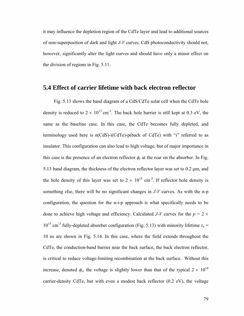
79
it may influence the depletion region of the CdTe layer and lead to additional sources
of non-superposition of dark and light J-V curves. CdS photoconductivity should not,
however, significantly alter the light curves and should have only a minor effect on
the division of regions in Fig. 5.11.
5.4 Effect of carrier lifetime with back electron reflector
Fig. 5.13 shows the band diagram of a CdS/CdTe solar cell when the CdTe hole
density is reduced to 2 × 1013 cm-3. The back hole barrier is still kept at 0.3 eV, the
same as the baseline case. In this case, the CdTe becomes fully depleted, and
terminology used here is n(CdS)-i(CdTe)-p(back of CdTe) with “i” referred to as
insulator. This configuration can also lead to high voltage, but of major importance in
this case is the presence of an electron reflector φe at the rear on the absorber. In Fig.
5.13 band diagram, the thickness of the electron reflector layer was set to 0.2 µm, and
the hole density of this layer was set to 2 × 1015 cm-3. If reflector hole density is
something else, there will be no significant changes in J-V curves. As with the n-p
configuration, the question for the n-i-p approach is what specifically needs to be
done to achieve high voltage and efficiency. Calculated J-V curves for the p = 2 ×
1013 cm-3 fully-depleted absorber configuration (Fig. 5.13) with minority lifetime τn =
10 ns are shown in Fig. 5.14. In this case, where the field extends throughout the
CdTe, the conduction-band barrier near the back surface, the back electron reflector,
is critical to reduce voltage-limiting recombination at the back surface. Without this
increase, denoted φe, the voltage is slightly lower than that of the typical 2 × 10¹⁴
carrier-density CdTe, but with even a modest back reflector (0.2 eV), the voltage

80
should increase significantly. Higher values of φe lead to only modest additional
improvement, and the thickness and carrier density of the reflector layer lead to only
minor variations in the J-V curves. Compare Fig. 5.14 with 5.10(b), one can find that
with the n-i-p configuration, when the lifetime is high, the presence of a large back
hole barrier φb only reduces the voltage, however, the presence of a back electron
reflector φe improve the voltage significantly.
Fig. 5.13: Band diagram for low carrier density (n-i-p structure) with and without a back electron reflector.
81
Fig. 5.14: Simulated J-V curves for n-i-p structure with and without a back electron reflector. CdTe minority lifetime is high at 10 ns.
Fig. 5.15 shows that when the electron-reflector barrier is present, the CdTe
lifetime needs to be respectable, but need not be particularly high, to achieve a high
voltage. One possibility for creating such a barrier is to add a layer of ZnTe or other
material with an expanded gap in the conduction-band direction. A potential
difficulty, however, is that even a small amount of recombination at the CdTe/ZnTe
or other reflector interface will compromise the advantage of keeping electrons away
from the metal interface. An electron barrier could of course be applied to CdTe that
is not fully depleted. In this case, however, the benefit of the barrier would be
relatively small, because the carrier densities at the back would not be large enough
for back recombination to significantly lower the voltage.

82
Fig. 5.15: Voltage dependence on lifetime and back electron barrier for n-i-p structure.
Fig. 5.16 shows the analogous effects of CdS/CdTe interfacial recombination
and conduction-band offset ∆Ec for the n-i-p structure compared with Fig. 4.13,
assuming the electron reflector discussed above is 0.2 eV. In the n-i-p case, the effect
of Voc with different interfacial recombination velocities vintf is intermediate, and at
the presumed value of ∆Ec (-0.1 eV), a small but finite vintf should be sufficient to
yield a high Voc.
Fig. 5.17 summarizes the two approaches to higher CdTe voltage. The
simulated n-p J-V curve corresponds to substantial increases in both CdTe lifetime
and hole density, τn = 100 ns and p = 2 ×1017 cm-3, the potential result of a greatly
reduced defect density as was described in Chap. 4. These parameters predict a
voltage of 1080 mV and an efficiency of 22% even if current losses in today’s record
cell are not reduced. This scenario, however, does assume that one can construct a

83
more favorable conduction band offset or hold interfacial recombination to extremely
low values. The n-i-p simulation yields a somewhat similar J-V curve with a voltage
of 1030 mV and an efficiency of 21% at a moderate lifetime of 2 ns. It requires an
electron reflector the order of 0.2 eV in height near the back contact. In this case,
although the n-i-p structure would predict a high voltage, the fill factor will remain
lower than optimal unless the CdTe lifetime is significantly increased. Nevertheless,
this is probably the more practical strategy for improving voltage and performance,
since it should not require a major improvement in the quality of thin-film CdTe to
reach a voltage of one volt and an efficiency above 20%.
Fig. 5.16: Dependence of Voc on CdS/CdTe band offset and interfacial recombination for n-i-p structure.

84
Fig. 5.17: Comparison of record-cell J-V curve with possible curves using n-p an n-i-p strategies.
85
Chapter 6
Impact of a Secondary Front Barrier
6.1 Possible secondary front barrier for CdTe solar cells
The formation of a low-resistance, low-barrier back contact, discussed in the
previous chapter, is one of the most challenging aspects in the fabrication of a high-
performance CdTe solar cell. In this chapter, we will move to the front part of a CdTe
solar cell, the TCO, CdS, and CdTe interfaces. The questions are whether it is
possible to have a secondary front barrier in CdTe solar cell, how we can distinguish
it from a back barrier, and what happens if such a front barrier exists?
In CIS and CIGS solar cells, secondary front barriers have been observed [33,
57], and are the result of the positive conduction-band discontinuity (spike) at the
CdS/CI(G)S interface. This front barrier is responsible for current limitation and can
significantly reduce the fill factor [57]. The energy difference between the conduction
band and quasi-Fermi level for electrons at CdS/CI(G)S interface is the key value to
explain the J-V distortion [33].

86
For CdTe based solar cells, from the theoretical point of view, there can be
several possible causes for a front barrier: (i) high conduction-band-offset (CBO)
between TCO and CdS layer; (ii) a highly photoconductive CdS layer; and (iii) a
dipole CdS layer with the electric field opposing that of the CdTe layer [58, 59]. We
will discuss the possibility of these three causes and their impact on cell performance
in the following.
6.2 Impact of conduction-band offset at TCO/CdS interface
Several TCO materials have been tested as a front contact for CdTe based solar
cells. The best energy conversion efficiencies to date have been obtained with SnO2
contacts. A negligible conduction-band-discontinuity was inferred from the
experiments by Niles et al. [60]. Additionally, the Fermi level at the SnO2/CdS
interface is 0.2 eV below the conduction band, and hence no large barrier height for
electron transport across the interface should be present. Therefore, the SnO2/CdS
contact can be a reasonably ideal front contact. Fritsche et al. [61, 62] confirm that
the band alignment at SnO2/CdS can be considered as ideal for front contact
formation, but the Fermi-level can be well below the conduction band edge at the
interface as a result of charged interface states. We will discuss the charged
SnO2/CdS interface states in the region of a possible dipole CdS layer. Here, the
question is that if the TCO layer is not an ideal contact, and the conduction-band-
offset at TCO/CdS interface is no longer negligible, what happens to the cell
performance.
87
Fig. 6.1 shows the calculated PV parameters as a function of ∆Ec at TCO/CdS
interface. Voc is almost unchanged with various conduction-band-offset. Jsc is also
almost constant except that the value becomes extremely low when ∆Ec is above 0.5
eV. This is because with such high, positive conduction-band-offset (big spike), the
depletion region in the bulk CdTe becomes very thin, which leads to a very small
photocurrent collection and therefore, a photocurrent is significantly reduced. Fill
factor and efficiency are almost constant when ∆Ec is in the range of -0.4 eV to 0.4
eV, and beyond this range, they begin to decrease due to critical barrier for both
forward and photogenerated reverse currents. The reduction of FF and η in the spike
region is much more critical than that in the cliff region, especially when ∆Ec is above
0.5 eV, where photocurrent is significantly lower.

88
Fig. 6.1: Calculated PV parameters as a function of ∆Ec at the TCO/CdS interface.
Ref. [60] predicts a negligible SnO2/CdS offset, and Fig. 6.1 shows that even if
the conduction-band-offset at TCO/CdS interface is not negligible, the cell
performance would not change much, at least in the range of -0.4 eV to 0.4 eV.

89
6.3 Impact of CdS photoconductivity
There appears to be little information on specific electronic properties of CdS
films in CdS/CdTe solar cells. The recipes for CdS in solar cells do not generally
include any intentional doping. Therefore the doping of the CdS is largely determined
during cell fabrication such as the post-deposition CdCl2 treatment and the inclusion
of Cu in the back contact. Pure CdS is an n-type material. However, Cl impurities,
which should form shallow donor states, and Cu impurities, which should form deep
acceptor defect states, are found in the typical CdS layer. A photoconductive region
in the CdS layer is produced by the diffusion of Cu into CdS, since it can compensate
the nomally n-type material. In the BL case, we assume that the CdS layer is highly
compensated n-type with the shallow donor density greater than the deep acceptor
defects density. In this section we will discuss the photoconductivity effects of CdS
due to the changes in net charge density.
Fig. 6.2 shows the conduction band calculated at zero bias in the dark and under
illumination with different shallow donor densities ND in CdS layer. The deep
acceptor defect density in CdS was unchanged for all the three cases (NAD = 1 × 10¹⁸
cm-3). With a small shallow donor density, CdS becomes more p-type, hence the
barrier in CdS layer is pushed up and the depletion width in CdTe is reduced. For
both the baseline case (ND = 1.1 × 1018 cm-3) and n+-CdS case (ND = 1 ×1019 cm-3),
there is no difference between the bands in the dark and in the light. However, when
the shallow donor density is reduced to 1× 1017 cm-3, the barrier in CdS is much lower
in the light than that in the dark since the light generates free electrons and neutralizes

90
a great number of deep defect accepters in CdS, which causes a less p-doped CdS and
a wider CdTe depletion width.
Fig. 6.2: Conduction band calculated at zero bias in the dark and under illumination with different shallow donor densities ND in CdS layer.
The resulting dark and light J-V curves are shown in Fig. 6.3. In the light, when
the shallow donor density is reduced, there is only a small amount of reduced fill
factor and reduced forward current. The former is due to the small amount of reduced
depletion width in CdTe, and the latter is due to the small amount of increased barrier
in CdS. In the dark, however, the current is greatly reduced in forward bias, since the
barrier in CdS is much higher when ND = 1× 1017 cm-3. The dark and light J-V curves
show a large crossover. In summary, the photoconductivity of CdS can lead to major
dark/light crossover, but it only has weak effect on light J-V performance.

91
Fig. 6.3: Dark and light J-V curves with different shallow donor densities ND in CdS layer.
6.4 Impact of a dipole CdS layer
A pressure effect referred as piezo-effect, which was observed by Shvydka et
al. [58], predicts a strong electric field throughout the CdS layer in the direction
opposite that of the junction field. Such a reverse electric field could cause a front
barrier, shown in Fig. 5(b) in ref. [58]. The physical model of CdS which undergoes
the piezo-effect was then explored by Cooray and Karpov [59]. They proposed a
metal-insulator-semiconductor (MIS) structure, where CdS plays the role of insulator
and the electric field throughout it is reversed. This physical model was solved
analytically and verified numerically. It explains some observed phenomena, such as
the lack of carrier collection from CdS, buffer layer effects, and crossover and
rollover of the J-V curves. In this section, we will use the numerical method to

92
simulate a dipole CdS layer with the reversed electric field, and the resulting J-V
performance as a function of the front barrier from a possible CdS dipole will be
evaluated.
For simulation of the dipole CdS model, the parameters used in the TCO
buffer layer and the bulk CdTe layer will generally be the same as the baseline case.
For the dipole itself, two narrow layers (5-nm thickness for each) containing high
concentrations of shallow acceptors (NA) or donors (ND) of equal magnitude were
added to the opposite sides of the CdS layer. Recombination centers were not
included in the two narrow interfacial layers. The negative and the positive charge
densities were therefore large and equal in magnitude, and hence forming two-
dimensional sheet charges each with area density σ. High concentrations of acceptors
at TCO/CdS interface are plausible, since Cu concentration can increase dramatically
at the TCO/CdS interface [63]. As a consequence, Fig. 6.4, a dipole CdS layer with
negative and positive charges at both sides may be established. The conduction band
is increased near TCO/CdS interface and reduced near CdS/CdTe interface, and the
electric field is reversed throughout the CdS layer. The front barrier φf is produced as
a result. Fig. 6.4 also shows that the Fermi-level is well below the conduction band
edge at the TCO/CdS interface as a result of charged interface states. This is also
possible and has been reported by Fritsche et al. [61, 62].

93
Fig. 6.4: Dipole CdS with negative and positive space charges at both sides of CdS; φf refers to the front barrier.
The calculated magnitude of front barrier as a function of the dipole sheet
charge density σ in the light at zero bias is shown in Fig. 6.5. φf (light, V = 0)
increases with the dipole charges more quite steeply above σ = 2 × 1012 cm-2. In the
following, the light J-V behavior will be discussed as a function of the front barrier in
the light at zero bias. The dark J-V curve with high front barrier still shows the greatly
reduced forward current and even cross-over between dark and light as expected, and
hence will not be discussed further in this section.
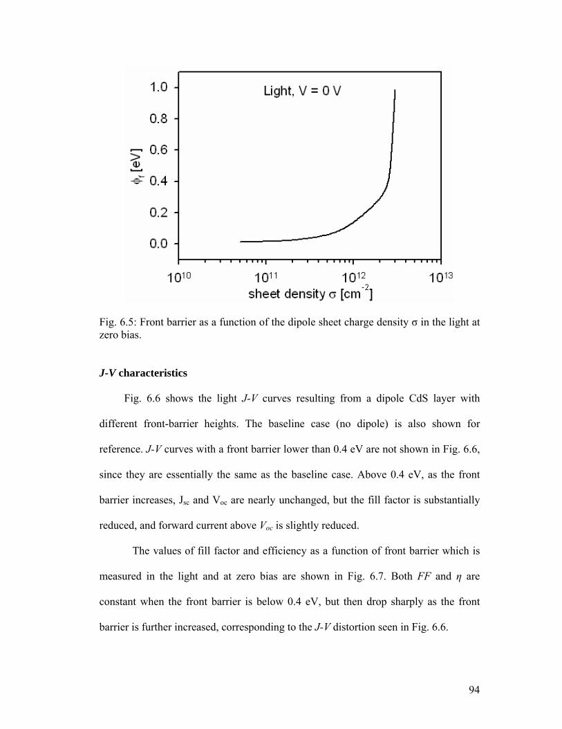
94
Fig. 6.5: Front barrier as a function of the dipole sheet charge density σ in the light at zero bias.
J-V characteristics
Fig. 6.6 shows the light J-V curves resulting from a dipole CdS layer with
different front-barrier heights. The baseline case (no dipole) is also shown for
reference. J-V curves with a front barrier lower than 0.4 eV are not shown in Fig. 6.6,
since they are essentially the same as the baseline case. Above 0.4 eV, as the front
barrier increases, Jsc and Voc are nearly unchanged, but the fill factor is substantially
reduced, and forward current above Voc is slightly reduced.
The values of fill factor and efficiency as a function of front barrier which is
measured in the light and at zero bias are shown in Fig. 6.7. Both FF and η are
constant when the front barrier is below 0.4 eV, but then drop sharply as the front
barrier is further increased, corresponding to the J-V distortion seen in Fig. 6.6.

95
Fig. 6.6: Light J-V curves resulting from a dipole CdS layer with different front barrier heights which are measured in the light at zero bias. The baseline case is shown for reference.
Fig. 6.7: Calculated fill factor and efficiency as a function of front barrier.
96
Explanation
Electron current can be significantly reduced by the front barrier, and is
responsible for the J-V distortion. The hole current has no direct role.
Assuming thermionic emission across the barrier, the electron current density Jn
can be calculated by integrating over the product of carrier density and carrier
velocities in the direction of transport. And the integral can be simplified by:
thn qnvJ = (6.1)
where vth is the thermal velocity of electrons about 107 cm/s, q is the electron charge
and n is the free electron density given by:
⎟⎠⎞
⎜⎝⎛ −−=
kTEE
Nn FnCC exp . (6.2)
NC is the effective density of states in the conduction band, k is the Boltzmann
constant, and T is the absolute temperature. Thus, at a fixed temperature, the electron
current through the junction is determined by n and therefore by the energy difference
between the conduction band and quasi-Fermi level. An increase of this energy
difference will result in fewer electrons, and hence possible current reduction.
Typical photocurrent density achieved in the power quadrant for CdS/CdTe
cells is about 24 mA/cm2 for 1-sun illumination. According to equation (6.1), the
minimum electron density to provide the current flow is 1.5 × 1010 cm-3, which
corresponds to 0.49-eV difference between conduction band and quasi-Fermi level
for electrons. If EC – EFn is lower than this value, n is sufficient to provide the
photocurrent, but if EC – EFn exceeds this value, additional drift fields are required to
help the electron transition. The values are calculated for the particular choice of

97
parameters used in simulations, and for lower temperatures, a smaller value of EC –
EFn is required.
Fig. 6.8 calculates the value of EC – EFn in the light at zero bias for various front
barriers. It shows that the maximum EC – EFn is located at or near TCO/CdS interface,
and it is therefore the key value for the electron current transport. The calculations of
EC – EFn at the TCO/CdS interface for different voltage bias in the light are shown in
Fig. 6.9. Below Voc, with front barrier of 0.4 eV, EC – EFn is constant and well below
0.49 eV at low biases, and then decreases as the voltage bias approaches Voc. The
decrease in EC – EFn results the increase forward electron current, and therefore a
somewhat reduced fill factor. For the 0.5-eV front barrier, the situation is similar,
except that the drop of EC – EFn is large, and the result is a greater reduction in fill
factor. When the front barrier is increased to 0.6 eV and 0.7 eV, EC – EFn increases
with voltage bias before it drops below Voc. This causes the reduced photocurrent and
thus still lower fill factor and more severe J-V distortion. Above Voc, EC – EFn
decreases sharply with voltage bias, corresponding to the steep increase in forward
current in forward bias. For higher front barriers, EC – EFn is higher, and hence the
forward current above Voc is lower.
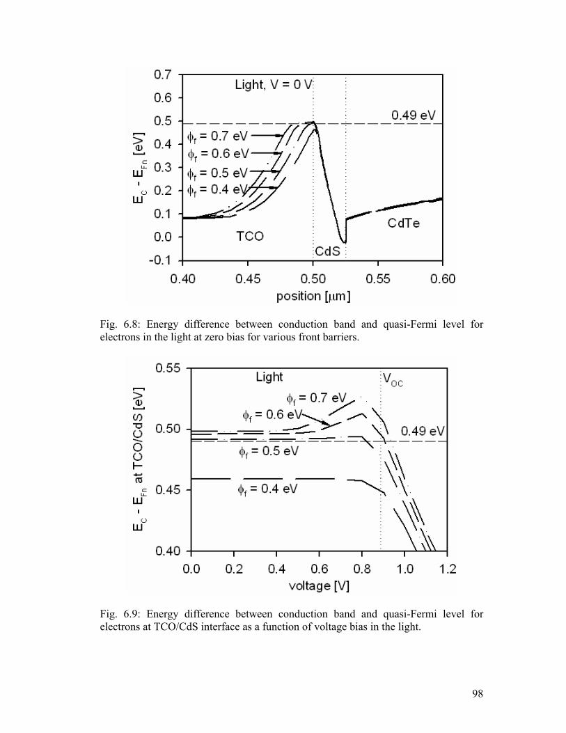
98
Fig. 6.8: Energy difference between conduction band and quasi-Fermi level for electrons in the light at zero bias for various front barriers.
Fig. 6.9: Energy difference between conduction band and quasi-Fermi level for electrons at TCO/CdS interface as a function of voltage bias in the light.
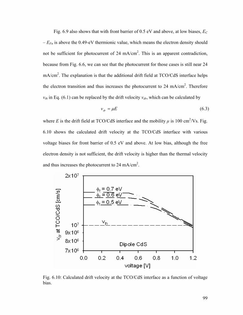
99
Fig. 6.9 also shows that with front barrier of 0.5 eV and above, at low biases, EC
– EFn is above the 0.49-eV thermionic value, which means the electron density should
not be sufficient for photocurrent of 24 mA/cm2. This is an apparent contradiction,
because from Fig. 6.6, we can see that the photocurrent for those cases is still near 24
mA/cm2. The explanation is that the additional drift field at TCO/CdS interface helps
the electron transition and thus increases the photocurrent to 24 mA/cm2. Therefore
vth in Eq. (6.1) can be replaced by the drift velocity vdr, which can be calculated by
Evdr µ= (6.3)
where E is the drift field at TCO/CdS interface and the mobility µ is 100 cm2/Vs. Fig.
6.10 shows the calculated drift velocity at the TCO/CdS interface with various
voltage biases for front barrier of 0.5 eV and above. At low bias, although the free
electron density is not sufficient, the drift velocity is higher than the thermal velocity
and thus increases the photocurrent to 24 mA/cm2.
Fig. 6.10: Calculated drift velocity at the TCO/CdS interface as a function of voltage bias.

100
Other variations
The above discussion mainly focused on a possible dipole CdS layer. If a
monopole CdS with only one type of interfacial space charge were present, it also
could produce the reversed electric field in CdS layer. Either a negative or a positive
monopole is possible. If only negative space charge is generated between TCO and
CdS, the situation will be similar to the dipole. If the negative charge generates a
reversed electric field in CdS layer and produces a high front barrier, the J-V curve
will show distortion. If only positive charge is generated between CdS and CdTe, the
J-V curve should be the same as the baseline case, since although there is field
reversal in CdS, no front barrier is generated in this situation.
If the total thickness of CdS is increased, the thickness of the two dipole charge
sheets will be increased to produce a strongly depleted CdS with the reversed electric
field. The details of J-V curves will be different, and the general features of the
distortion will be similar.
The TCO layer has been assumed to be conductive with a carrier density the
order of 1017 cm-3. If this layer has higher carrier density, the J-V characteristics are a
little bit different. Fig. 6.11 compares the fill factor and efficiency with different
carrier densities in TCO layer. When the carrier density in TCO is increased to 1020
cm-3, J-V distortion would require higher front barrier around 0.6 eV. Voc and Jsc
would still remain constant.
Variations in CdTe layer do not change the general principle discussed above,
and will not be discussed in detail here. In summary, a large secondary front barrier
formed by a possible dipole CdS layer could substantially reduce the fill factor and

101
efficiency, which is resulted from the severe J-V distortion below Voc, and slightly
reduce the forward current above Voc.
Fig. 6.11: Comparison of fill factor and efficiency for different carrier densities in TCO layer.

102
Chapter 7
Conclusions
Carrier lifetimes and secondary barriers are key factors governing J-V
behavior in CdTe solar cells. Here, the secondary barriers refer to: (i) the Schottky
back hole barrier, which is due to the low work function of the back metal contact; (ii)
the back electron reflector which could be created by adding a layer of ZnTe or other
material with an expanded gap in the conduction-band direction; and (iii) the front
barrier which could be produced by the high conduction-band offset at TCO/CdS
interface, a highly photoconductive CdS layer, or a dipole CdS layer in which the
electric field is reversed.
The carrier-lifetime/back-hole-barrier space can be divided into four regions
with four different types of J-V characteristics. When the back barrier is sufficiently
low to have little effect, the space can be divided into: (a) high recombination in the
space-charge region and reduced fill factor due to low carrier lifetimes, and (b) high
electron current and enhanced fill factor due to high carrier lifetimes. Increasing
lifetime leads to increasing fill factor and increasing voltage, but only up to a point

103
for typical carrier-density CdTe. If the CdTe carrier density is increased above the
typical 2 × 1014 cm-3, the voltage will increase, although the photocurrent can be
reduced due to narrow depletion region if the lifetime is not high. Hence, both high
lifetime and high carrier density are required for high voltage in the standard n-p
configuration. Compared with the 16.5% record CdTe solar cell, the simulated n-p J-
V curve calculated with substantial increases in CdTe lifetime (100 ns) and hole
density (2 × 1017 cm-3), has a voltage of 1080 mV and an efficiency of 22% even if
current losses in today’s record cell are not reduced. It does, however, assume that
one can construct a more favorable conduction band offset or hold interfacial
recombination to extremely low values.
When the back-contact barrier is large enough to affect the current transport,
the features of the remaining two regions are significantly altered. Under high SCR-
recombination conditions, region (c), in which the total current is limited by the hole
current at the back contact and saturates at forward bias, exhibits J-V “rollover”.
Under high electron-injection conditions, region (d) is defined as “back-contact
enhanced electron current” where J-V curves show reduced Voc and enhanced electron
current in the light. In this case, photo-generated holes are blocked by the high back
contact, and the electron injection at the front junction is enhanced. A significant
feature of region (d) is a crossover of light and dark J-V curves. Overlap of front and
back space-charge regions is a subset of region (d), but is not a requirement for
reduced Voc.
If the carrier density is reduced to 2 × 1013 cm-3, the absorber will be fully
depleted and the model is referred as the n-i-p configuration. This model allows

104
higher minority-electron injection at the back contact, and therefore results in
increased forward current and reduced voltage. However, if an effective electron
reflector can be constructed at the back contact, the voltage should be increased,
because the reflector would keep the minority carriers away from the back contact. In
this case, the lifetimes for high efficiency need not to be particularly high. The n-i-p
simulation yields a J-V curve with a voltage of 1030 mV and an efficiency of 21% at
a moderate lifetime of 2 ns. It requires an electron reflector the order of 0.2 eV in
height near the back contact. In this case, although the n-i-p structure would predict a
high voltage, the fill-factor will remain lower than optimal unless the CdTe lifetime is
increased somewhat over current values. Nevertheless, this is probably the more
practical strategy for improving voltage and performance, since it should not require a
major improvement in the quality of thin-film CdTe to reach one volt and 20%.
A secondary front barrier in CdS/CdTe solar cell may be produced by the
following ways: high conduction-band offset at TCO/CdS interface, highly
photoconductive CdS layer, or a dipole CdS layer. The cell performance would not
change much when the conduction band offset at TCO/CdS interface is in the range
of -0.4 eV to 0.4 eV, but beyond this region, J-V distortion would take place. The
reduction of fill factor and efficiency in the spike region is much more critical than
that in the cliff region. The photoconductivity of CdS can lead to dark and light
crossover, but it only has weak effect on light J-V performance. A large front barrier
formed by a dipole CdS layer could result in reduced fill factor and efficiency. When
the front barrier is above 0.4 eV, J-V distortion becomes appreciable. The key value is
the maximum energy difference between the conduction band and the quasi-Fermi

105
level for electrons at the TCO/CdS interface where the peak of the front barrier is
located. It determines if there are sufficient free electrons to provide the required
photocurrent. Otherwise, an additional drift field is required to help the electron
transition. The increase of EC – EFn with voltage bias causes the reduced photocurrent,
and hence the J-V distortion.
The CdS/CdTe cell is a very complex system. All of these mechanisms
mentioned above interact with each other to some degree, and many of them work
together to determine the cell performance. Therefore, during analysis process, which
mechanism dominates should depend on specific materials and geometric properties
as well as the operation conditions.

106
Bibliography
[1] K. Zweibel, Solar Energy Mat. and Solar Cells, 59, 1 (1999). [2] K. Zweibel, Solar Energy Mat. and Solar Cells, 63, 375(2000). [3] D. M. Chapin, C. S. Fuller, and G. L. Pearson, J. Appl. Phys., 25, 676 (1954). [4] D. C. Raynolds, G. Leies, L. L. Antes, and R. E. Marburger, Phys. Rev., 96, 533
(1954). [5] T. Surek, in Proceedings of the 3rd World Conference of Photovoltaic Energy
Conversion (2003), p. 8PL-E3-01. [6] J. Zhao, A. Wang, and M. A. Green, Prog. Photovoltaics 7, 471 (1999). [7] X. Wu, J. C. Keane, R. G. Dhere, C. DeHart, D. S. Albin, A. Duda, T. A. Gessert,
S. Asher, D. H. Levi, and P. Sheldon, in Proceedings of the 17th European Photovoltaic Solar Energy Conference (2001), p. 995.
[8] M. A. Contreras, K. Ramanathan, J. AbuShama, F. Hasoom, D. L. Young, B.
Egaas, and R. Noufi, Prog. Photovoltaics 13, 209 (2005). [9] M. A. Green, in Proceedings of the 3rd World Conference of Photovoltaic Energy
Conversion (2003), p. OPL-02. [10] V. Parente, J. Goldemberg, and R. Zilles, Prog. Photovoltaics 10, 571 (2002). [11] National Renewable Energy Laboratory, What is the energy payback for PV?
http://www.nrel.gov/docs/fy05osti/37322.pdf [12] National Renewable Energy Laboratory, Will we have enough materials for
energy-significant PV production? http://www.nrel.gov/docs/fy04osti/35098.pdf
[13] D. A. Neamen, Semiconductor Physics and Devices: Basic Principles, 3rd ed.
(McGraw-Hill, New York, 2003).

107
[14] S. M. Sze, Physics of Semiconductor Devices, 2nd ed. (Wiley, New York, 1981). [15] S. S. Hegedus and W. N. Shafarman, Prog. Photovoltaics 12, 155 (2004). [16] R. N. Hall, Phys. Rev. 83, 228 (1951). [17] W. Shockley and W. T. Read, Phys. Rev. 87, 835 (1952). [18] A. M. Hermann, Solar Energy Mat. and Solar Cells 55, 75 (1998). [19] H. S. Ullal, K. Zweibel, and B. von Roedern, in Proceedings of the 26th IEEE
Photovoltaic Specialists Conference (1997), p. 301.
[20] S. R. Kurtz, J. M. Olson, and A. Kibbler, in Proceedings of the 21st IEEE Photovoltaic Specialists Conference (1990), p. 138.
[21] S. H. Demtsu and J. R. Sites, in Proceedings of 31st IEEE Photovoltaic Specialists Conference (2005), p. 347.
[22] D. Friedman, I. Lindau, and W. Spicer, Phys. Rev. B 37, 731 (1987). [23] Y. Bilevych, A. Sukach, and V. Tetyorkin, Phys. Stat. Sol. C 1, 317 (2004). [24] T. Chu, S. Chu, and S. Ang, J. Appl. Phys. 58, 4296 (1985). [25] H. Toyoma et al., Jpn. J. Appl. Phys. 43, 6371 (2004). [26] G. Stollwerch and J. R. Sites, in Proceedings of the 13th European Photovoltaic
Solar Energy Conference (1995), p. 2020. [27] A. Niemegeers and M. Burgelman, J. Appl. Phys. 81, 2881 (1997). [28] B. E. McCandless, J. E. Phillips, and J. Titus, in Proceedings of the 15th
European Photovoltaic Solar Energy Conference (1998), p. 448. [29] S. H. Demtsu and J. R. Sites, Thin Solid Films 510, 320 (2006). [30] C. R. Corwine, A. O. Pudov, M. Gloeckler, S. H. Demtsu, and J. R. Sites, Solar
Energy Mat. and Solar Cells, 82, 481 (2004).
[31] H. Zhu, A. K. Kalkan, J. Hou, and S. J. Fonash, in Proceedings of National Center for Photovoltaics (NCPV) 15th Program Review Meeting (1999), 462, p. 309.
[32] M. Gloeckler and J. R. Sites, J. Appl. Phys. 95, 4438 (2004).
108
[33] A. Kanevce, M. Gloeckler, A. O. Pudov, and J. R. Sites, Mat. Res. Soc. Symp.
Proc. 865, 221 (2005).
[34] S. Tripathi, N. Venkataramani, R. O. Dusane, and B. Schroeder, Thin Solid Films 501, 295 (2006).
[35] A. Niemegeers and M. Burgelman, in Proceedings of 25th IEEE Photovoltaic
Specialists Conference (1996), p. 901.
[36] A. Niemegeers, S. Gillis, and M. Burgelman, in Proceedings of the 2nd World Conference on Photovoltaic Energy Conversion (1998), p. 672.
[37] M. Burgelman, P. Nollet, and S. Degrave, Thin Solid Films 361 – 362, 527
(2000). [38] M. Burgelman, J. Verschraegen, S. Degrave, and P. Nollet, Prog. Photovoltaics
12, 143 (2004). [39] S. Degrave, M. Burgelman, and P. Nollet, in Proceedings of 3rd World
Conference on Photovoltaic Energy Conversion (2003), p. 2P-D3-50.
[40] M. Gloeckler, A. L. Fahrenbruch, and J. R. Sites, in Proceedings of the 3rd World Conference on Photovoltaic Energy Conversion (2003), p. 491.
[41] Supplied by D. Albin, National Renewable Energy Laboratory. [42] K. Emery, Handbook of Photovoltaic Science and Engineering, edited by A.
Luque and S. S. Hegedus (Wiley, New York, 2003), p. 702 – 711. [Based on R. Bird, R. Hulstrom, and C. Riordan, Solar Cells 14, 193 (1985)].
[43] S. H. Wei, S. B. Zhang, and A. Zunger, J. Appl. Phys. 87, 1304 (2000).
[44] R. K. Ahrenkiel, B. M. Keyes, L. Wang, and S. P. Albright, in Proceedings of 22nd IEEE Photovoltaic Specialists Conference (1991), p. 940.
[45] R. K. Ahrenkiel and S. W. Johnston, Materials Science and Engineering B 102,
161 (2003). [46] W. K. Metzger, D. Albin, D. Levi, P. Sheldon, X. Li, B. M. Keyes, and R. K.
Ahrenkiel, J. Appl. Phys. 94, 3549 (2003). [47] S. S. Hegedus, Prog. Photovoltaics 5, 151 (1997). [48] M. Gloeckler and J. R. Sites, in Proceedings of 19th European Photovoltaic Solar
Energy Conference (2004), p. 1863.

109
[49] M. Gloeckler and J. R. Sites, Thin Solid Films 480 – 481, 241 (2005). [50] J. Fritsche, T. Schulmeyer, D. Kraft, A. Thissen, A. Klein, and W. Jaegermann,
Appl. Phys. Lett. 81, 2297 (2002).
[51] T. A. Gessert, M. J. Romero, S. Johnson, B. Keyes, and P. Dippo, in Proceedings of 29th IEEE Photovoltaic Specialists Conference (2002), p. 535.
[52] J. Beier, M. Köntges, P. Nollet, S. Degrave, and M. Burgelman, Mat. Res. Soc.
Symp. Proc. 668, H9.5.1 (2001). [53] M. Burgelman, P. Nollet, and S. Degrave, in Proceedings of 28th IEEE
Photovoltaic Specialists Conference (2000), p. 551.
[54] Y. Roussillon, V. G. Karpov, D. Shvydka, J. Drayton, and A. D. Compaan, J. Appl. Phys. 96, 7283 (2004).
[55] S. S. Hegedus and B. E. McCandless, Sol. Energy Mater. Sol. Cells 88, 75
(2005). [56] M. Gloeckler, J. R. Sites, and W. K. Metzger, J. Appl. Phys. 98, 113704 (2005).
[57] A. O. Pudov, A. Kanevce, H. A. Al-Thani, J. R. Sites, and F. S. Hasoon, J. Appl.
Phys. 97, 064901 (2005). [58] D. Shvydka, J. Drayton, A. D. Compaan, and V. G. Karpov, Appl. Phys. Lett. 87,
123505 (2005).
[59] L. Cooray and V. G. Karpov, Appl. Phys. Lett. 88, 093508 (2006). [60] D. W. Niles, D. Rioux, and H. Höchst, J. Appl. Phys. 73, 4586 (1993). [61] J. Fritsche, S. Gunst, A. Thiβen, R. Gegenwart, A. Klein, and W. Jaegermann,
Mat. Res. Soc. Symp. Proc. 668, H5.1.1 (2001). [62] J. Fritsche, D. Kraft, A. Thiβen, T. Mayer, A. Klein, and W. Jaegermann, Thin
Solid Films 403 – 404, 252 (2002). [63] Y. Yan, K. Jones, X. Wu, and M. Al-Jassim, MRS Spring Meeting (2007), Y4.9,
in press.