Embed Size (px)
Citation preview

The content and copyrights of the attached material are the property of its owner.
Distributed by:
www.Jameco.com ✦ 1-800-831-4242
1/29
¡ Semiconductor MSM80C85AHRS/GS/JS
GENRAL DESCRIPTION
The MSM80C85AH is a complete 8-bit parallel; central processor implemented in silicon gateC-MOS technology and compatible with MSM80C85A.It is designed with higher processing speed (max.5 MHz) and lower power consumptioncompared with MSM80C85A and power down mode is provided, thereby offering a high levelof system integration.The MSM80C85AH uses a multiplexed address/data bus. The address is split between the 8-bit address bus and the 8-bit data bus. The on-chip address latch : of a MSM81C55-5 memoryproduct allows a direct interface with the MSM80C85AH.
FEATURES
• Power down mode (HALT-HOLD)• Low Power Dissipation: 50mW(Typ)• Single + 3 to + 6 V Power Supply• –40 to + 85°C, Operating Temperature• Compatible with MSM80C85A• 0.8 ms instruction Cycle (VCC = 5V)• On-Chip Clock Generator (with External Crystal)• On-Chip System Controller; Advanced Cycle Status Information Available for Large System
Control• Bug operation in MSM80C85AH is fixed• Four Vectored interrupt (One is non-maskable) Plus the 8080A-compatible interrupt.• Serial, In/Serial Out Port• Decimal, Binary and Double Precision Arithmetic• Addressing Capability to 64K Bytes of Memory• TTL Compatible• 40-pin Plastic DIP(DIP40-P-600-2.54): (Product name: MSM80C85AHRS)• 44-pin Plastic QFJ(QFJ44-P-S650-1.27): (Product name: MSM80C85AHJS)• 44-pin Plastic QFP(QFP44-P-910-0.80-2K): (Product name: MSM80C85AHGS-2K)
¡ SemiconductorMSM80C85AHRS/GS/JS8-Bit CMOS MICROPROCESSOR
E2O0009-27-X2
This version: Jan. 1998Previous version: Aug. 1996
2/29
¡ Semiconductor MSM80C85AHRS/GS/JS
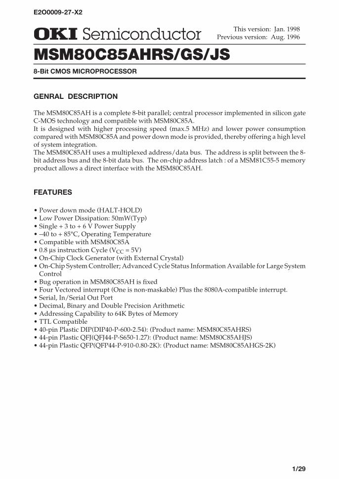
FUNCTIONAL BLOCK DIAGRAM
INTR INTA 5.5 6.5 7.5 TRAP SID SOD
RST
Power Down
Temporary Register(8)
Arithmetic Logic Unit
ALU(8)
Instruction Register (8)
InstructionDecoder
AndMachine
CycleEncoding
Flag (5)Flip Flops
CLKGEN
Timing And Control
Control Status DMA Reset Address Buffer (8)Data/Address
Buffer (8)
Stack Pointer (16)
Program Counter (16)
RegisterArray
Incrementer/Decrementer Address Latch (16)
H REG (8)
D REG (8)
B REG (8)
C REG (8)
E REG (8)
C REG (8)
8-Bit Internal Data Bus
X1
X2
CLKOUT
READY RD WR ALE S0 S1 IO / M HOLD HLDA RESET IN RESET OUT A15 - A8Address Bus
AD7 - AD0Address/Data Bus
Interrupt Control Serial I/O Control
Accumulator(8)
PowerSupply
+5VGND
3/29
¡ Semiconductor MSM80C85AHRS/GS/JS
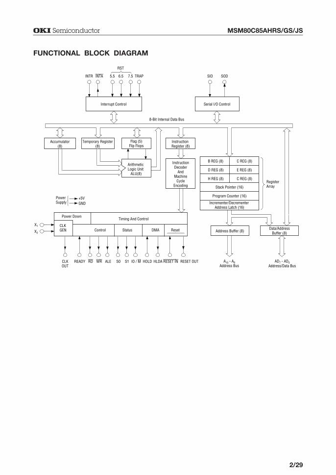
PIN CONFIGURATION (TOP VIEW)40 pin Plastic DIP
16151413
X1
20191817
GND
123456789
101112
32313029282726
37383940
36353433
25
A8
HOLDHLDACLK(OUT)RESET INREADYIO/MS1
RDWRALES0
A15
A14
A13
A12
A11
A10
A9
24232221
VCC
AD5
AD6
AD7
RST7.5RST6.5RST5.5
INTRINTAAD0
AD1
AD2
AD3
AD4
X2
RESET OUTSODSID
TRAP
44 pin Plastic QFP
39
38
37
36
35
34
33
READY
IO/M
S1
RD
WR
NC
ALE
TRAP
RST7.5
RST6.5
RST5.5
INTR
NC
INTA
18 19 20 21 22 23 24
AD4
NC
AD5
AD6
AD7
GN
D A 8
6 5 4 3 2 1 44
SID
SOD
RES
ET O
UT
X 2 X 1 NC
7
8
9
10
11
12
13
32
31
30
29
S0
A15
A14
AD0
AD1
AD2
AD3
14
15
16
17 A13
V CC
25 26 27 28
A 9 A 10
A 11
A 12
43 42 41 40
HO
LD
HLD
A
CLK(
OU
T)
RESE
T IN
44 pin Plastic QFJ
33
32
31
30
29
28
27
READY
IO/M
S1
RD
WR
ALE
S0
TRAP
RST7.5
RST6.5
RST5.5
INTR
INTA
AD0
12 13 14 15 16 17 18
AD4
AD5
AD6
AD7
GN
D
V CC A 8
44 43 42 41 40 39 38
SID
SOD
RES
ET O
UT
X 2 X 1 NC
1
2
3
4
5
6
7
26
25
24
23
A15
A14
A13
AD1
AD2
AD3
NC
8
9
10
11 A12
V CC
19 20 21 22
A 9 A 10
A 11
NC
37 36 35 34
HO
LD
HLD
A
CLK(
OU
T)
RESE
T IN
4/29
¡ Semiconductor MSM80C85AHRS/GS/JS
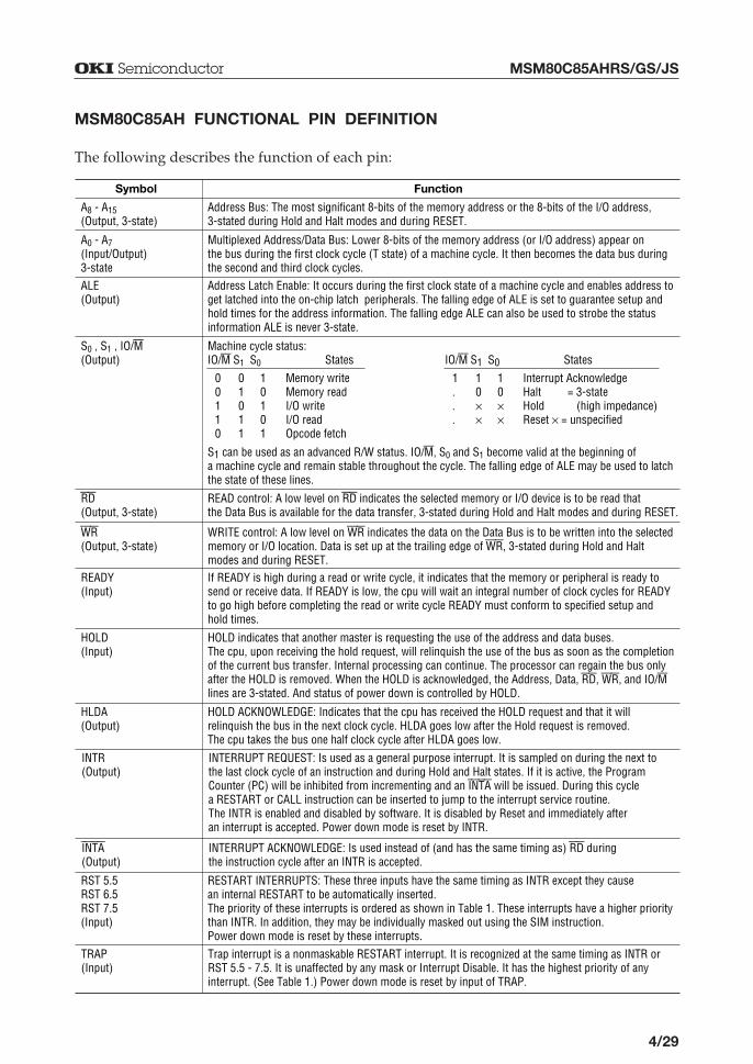
MSM80C85AH FUNCTIONAL PIN DEFINITION
The following describes the function of each pin:
A0 - A7(Input/Output)3-state
A8 - A15(Output, 3-state)
Multiplexed Address/Data Bus: Lower 8-bits of the memory address (or I/O address) appear on the bus during the first clock cycle (T state) of a machine cycle. It then becomes the data bus during the second and third clock cycles.
Address Bus: The most significant 8-bits of the memory address or the 8-bits of the I/O address, 3-stated during Hold and Halt modes and during RESET.
Symbol Function
ALE(Output)
Address Latch Enable: It occurs during the first clock state of a machine cycle and enables address to get latched into the on-chip latch peripherals. The falling edge of ALE is set to guarantee setup and hold times for the address information. The falling edge ALE can also be used to strobe the status information ALE is never 3-state.
S0 , S1 , IO/M(Output)
Machine cycle status: IO/M S1 S0 States
S1 can be used as an advanced R/W status. IO/M, S0 and S1 become valid at the beginning of a machine cycle and remain stable throughout the cycle. The falling edge of ALE may be used to latch the state of these lines.
RD(Output, 3-state)
READ control: A low level on RD indicates the selected memory or I/O device is to be read that the Data Bus is available for the data transfer, 3-stated during Hold and Halt modes and during RESET.
WR(Output, 3-state)
WRITE control: A low level on WR indicates the data on the Data Bus is to be written into the selected memory or I/O location. Data is set up at the trailing edge of WR, 3-stated during Hold and Halt modes and during RESET.
READY(Input)
If READY is high during a read or write cycle, it indicates that the memory or peripheral is ready to send or receive data. If READY is low, the cpu will wait an integral number of clock cycles for READY to go high before completing the read or write cycle READY must conform to specified setup and hold times.
HOLD(Input)
HLDA(Output)
HOLD ACKNOWLEDGE: Indicates that the cpu has received the HOLD request and that it will relinquish the bus in the next clock cycle. HLDA goes low after the Hold request is removed. The cpu takes the bus one half clock cycle after HLDA goes low.
HOLD indicates that another master is requesting the use of the address and data buses.The cpu, upon receiving the hold request, will relinquish the use of the bus as soon as the completion of the current bus transfer. Internal processing can continue. The processor can regain the bus only after the HOLD is removed. When the HOLD is acknowledged, the Address, Data, RD, WR, and IO/M lines are 3-stated. And status of power down is controlled by HOLD.
INTR(Output)
INTERRUPT REQUEST: Is used as a general purpose interrupt. It is sampled on during the next to the last clock cycle of an instruction and during Hold and Halt states. If it is active, the Program Counter (PC) will be inhibited from incrementing and an INTA will be issued. During this cycle a RESTART or CALL instruction can be inserted to jump to the interrupt service routine. The INTR is enabled and disabled by software. It is disabled by Reset and immediately after an interrupt is accepted. Power down mode is reset by INTR.
INTA(Output)
INTERRUPT ACKNOWLEDGE: Is used instead of (and has the same timing as) RD during the instruction cycle after an INTR is accepted.
RST 5.5RST 6.5RST 7.5(Input)
RESTART INTERRUPTS: These three inputs have the same timing as INTR except they cause an internal RESTART to be automatically inserted.The priority of these interrupts is ordered as shown in Table 1. These interrupts have a higher priority than INTR. In addition, they may be individually masked out using the SIM instruction. Power down mode is reset by these interrupts.
TRAP(Input)
Trap interrupt is a nonmaskable RESTART interrupt. It is recognized at the same timing as INTR or RST 5.5 - 7.5. It is unaffected by any mask or Interrupt Disable. It has the highest priority of any interrupt. (See Table 1.) Power down mode is reset by input of TRAP.
00110
01011
10101
Memory writeMemory readI/O writeI/O readOpcode fetch
IO/M S1 S0 States
1...
10¥¥
10¥¥
Interrupt AcknowledgeHalt = 3-stateHold (high impedance)Reset ¥ = unspecified
5/29
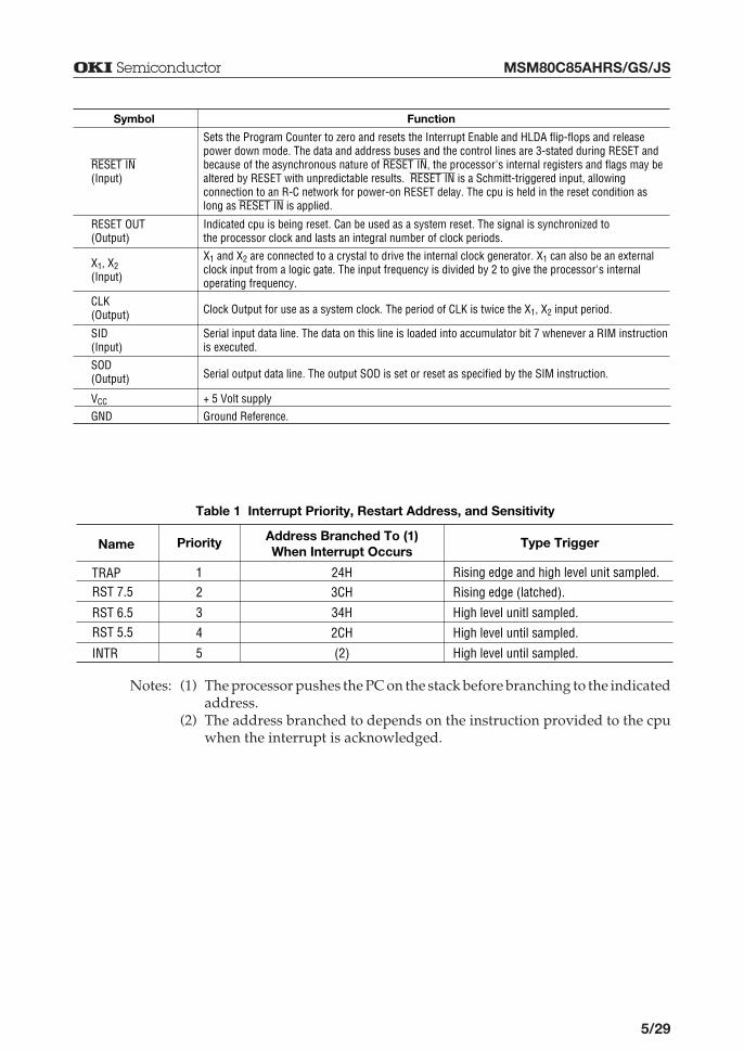
¡ Semiconductor MSM80C85AHRS/GS/JS
NameAddress Branched To (1)When Interrupt Occurs
Type Trigger
RST 7.5 3CH
34H
Rising edge (latched).
High level unitl sampled.RST 6.5RST 5.5 2CH
(2)
High level until sampled.
High level until sampled.INTR
TRAP
Priority
2
3
4
5
1 24H Rising edge and high level unit sampled.
Table 1 Interrupt Priority, Restart Address, and Sensitivity
Notes: (1) The processor pushes the PC on the stack before branching to the indicatedaddress.
(2) The address branched to depends on the instruction provided to the cpuwhen the interrupt is acknowledged.
RESET IN(Input)
Sets the Program Counter to zero and resets the Interrupt Enable and HLDA flip-flops and release power down mode. The data and address buses and the control lines are 3-stated during RESET and because of the asynchronous nature of RESET IN, the processor's internal registers and flags may be altered by RESET with unpredictable results. RESET IN is a Schmitt-triggered input, allowing connection to an R-C network for power-on RESET delay. The cpu is held in the reset condition as long as RESET IN is applied.
Symbol Function
RESET OUT(Output)
Indicated cpu is being reset. Can be used as a system reset. The signal is synchronized tothe processor clock and lasts an integral number of clock periods.
X1, X2(Input)
X1 and X2 are connected to a crystal to drive the internal clock generator. X1 can also be an external clock input from a logic gate. The input frequency is divided by 2 to give the processor's internal operating frequency.
SID(Input)
Serial input data line. The data on this line is loaded into accumulator bit 7 whenever a RIM instruction is executed.
SOD(Output) Serial output data line. The output SOD is set or reset as specified by the SIM instruction.
VCC + 5 Volt supply
GND Ground Reference.
CLK(Output) Clock Output for use as a system clock. The period of CLK is twice the X1, X2 input period.
6/29
¡ Semiconductor MSM80C85AHRS/GS/JS
FUNCTIONAL DESCRIPTION
The MSM80C85AH is a complete 8-bit parallel central processor. It is designed with silicon gateC-MOS technology and requires a single +5 volt supply. Its basic clock speed is 5 MHz, thusimproving on the present MSM80C85A's performance with higher system speed and powerdown mode. Also it is designed to fit into a minimum system of two IC's: The CPU(MSM80C85AH), and a RAM/IO (MSM81C55-5)
The MSM80C85AH has twelve addressable 8-bit register pairs. Six others can be usedinterchangeably as 8-bit registers or 16-bit register pairs. The MSM80C85AH register set is asfollows:
PC 16-bit address
8-bit ¥ 6 or 16-bits ¥ 3BC, DE, HLSP 16-bit address
5 flags (8-bit space)Flags or F
Program Counter
ACC or A 8-bitsAccumulator
Mnemonic ContentsRegister
General-Purpose Registers; data pointer (HL)
Stack Pointer
Flag Register
The MSM80C85AH uses a multiplexed Data Bus. The address is spilt between the higher 8-bitAddress Bus and the lower 8-bit Address/Data Bus. During the first T state (clock cycle) of amachine cycle the low order address is sent out on the Address/Data Bus. These lower 8-bitsmay be latched externally by the Address Latch Enable signal (ALE). During the rest of themachine cycle the data bus is used for mamory or I/O data.
The MSM80C85AH provides RD, WR, S0, S1, and IO/M signals for bus control. An InterruptAcknowledge signal (INTA) is also provided. Hold and all Interrupts are synchronized withthe processor's internal clock. The MSM80C85AH also provides Serial Input Data (SID) andSerial Output Data (SOD) lines for a simple serial interface.In addition to these features, the MSM80C85AH has three maskable, vector interrupt pins, onenonmaskable TRAP interrupt and power down mode with HALT and HOLD.
INTERRUPT AND SERIAL I/O
The MSM80C85AH has 5 interrupt inputs: INTR, RST 5.5 RST 6.5, RST 7.5, and TRAP. INTR isidentical in function to the 8080A INT. Each of the three RESTART inputs, 5.5, 6.5, and 7.5, hasa programmable mask. TRAP is also a RESTART interrupt but it is nonmaskable.
The three maskable interrupts cause the internal execution of RESTART ( saving the programcounter in the stack branching to the RESTART address) it the interrupts are enable and if theinterrupt mask is not set. The nonmaskable TRAP causes the internal execution of a RESTARTvector independent of the state of the interrupt enable or masks. (See Table 1.)
There are two different types of inputs in the restart interrupt. RST 5.5 and RST 6.5 are highlevel-sensitive like INTR (and INT on the 8080A) and are recognized with the same timing asINTR. RST 7.5 is rising edge-sensitive.

7/29
¡ Semiconductor MSM80C85AHRS/GS/JS
For RST 7.5, only a pulse is required to set an internal flip-flop which generates the internalinterrupt request. The RST 7.5 request flip-flop remains set until the request is serviced. Thenit is reset automatically, This flip-flop may also be reset by using the SIM instruction or byissuing a RESET␣ IN to the MSM80C85AH. The RST 7.5 internal flip-flop will be set by a pulseon the RST 7.5 pin even when the RST 7.5 interrupt is masked out.
The interrupts are arranged in a flixed priority that determines which interrupt is to berecognized if more than one is pending, as follows: TRAP-highest priority, RST 7.5, RST 6.5, RST5.5, INTR-lowest priority. This priority scheme does not take into account the priority of aroutine that was started by a higher priority interrupt. RST 5.5 can interrupt an RST 7.5 routineif the interrupt are re-enabled before the end of the RST 7.5 routine.
The TRAP interrupt is useful for catastrophic evens such as power failure or bus error. TheTRAP input is recognized just as any other interrupt but has the highest priority. It is notaffected by any flag or mask. The TRAP input is both edge and level sensitive. The TRAP inputmust go high and remain high until it is acknowledged. It will not be recognized again until itgoes low, then high again. This avoids any false triggering due to noise or logic glitches. Figure3 illustrates the TRAP interrupt request circuitry within the MSM80C85AH. Note that theservicing of any interrupt (TRAP, RST 7.5, RST 6.5, RST 5.5,INTR) disables all future interrupts(except TRAPs) until an El instruction is executed.
The TRAP interrupt is special in that it disables interrupts, but preserves the previous interruptenable status. Performing the first RIM instruction following a TRAP interrupt allows you todetermine whether interrupts were enabled or disabled prior to the TRAP. All subsequent RIMinstructions provide current interrupt enable status. Performing a RIM instruction followingINTR or RST 5.5-7.5 will provide current interrupt Enable status, revealing that Interrupts aredisabled.
The serial I/O system is also controlled by the RIM and SIM instructions. SID is read by RIM,and SIM sets the SOD data.
Inside the MSM80C85AHExternal TRAPInterrupt Request TRAP
SchmittTrigger
RESET IN RESETTRAP
InterruptRequest
+5 V D CLK
DQ
F/FClear
TRAP F.FInternalTRAP
Acknowledge
Figure 3 Trap and RESET IN Circuit
8/29
¡ Semiconductor MSM80C85AHRS/GS/JS
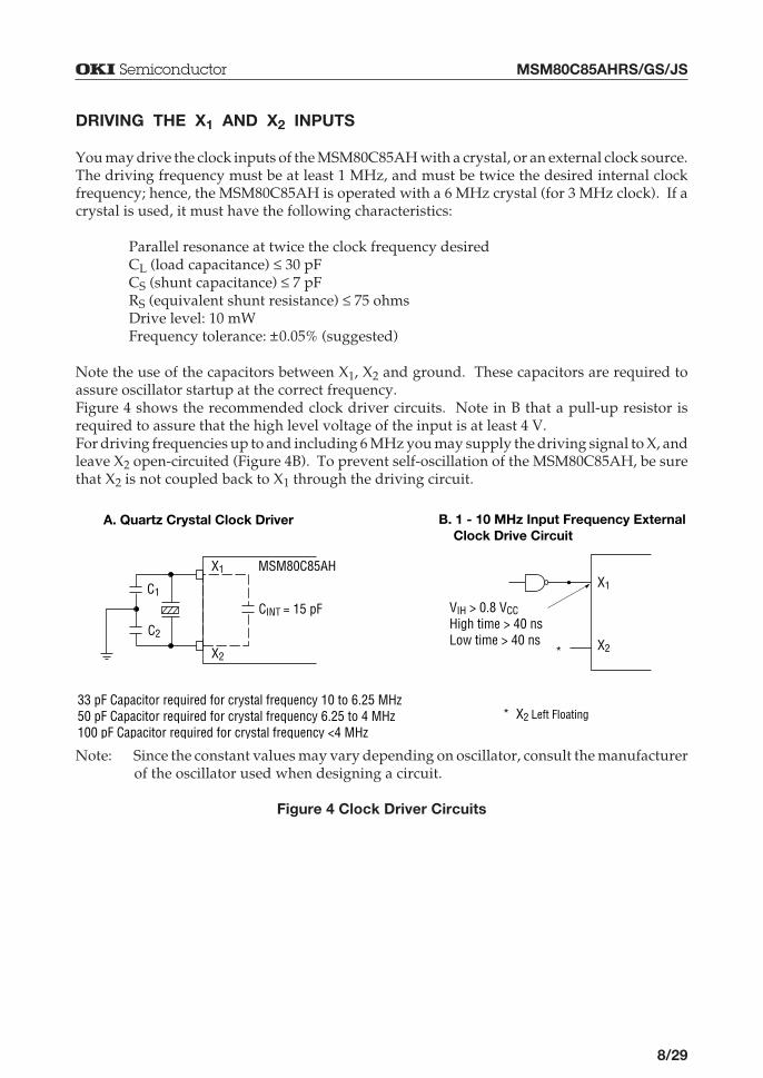
DRIVING THE X1 AND X2 INPUTS
You may drive the clock inputs of the MSM80C85AH with a crystal, or an external clock source.The driving frequency must be at least 1 MHz, and must be twice the desired internal clockfrequency; hence, the MSM80C85AH is operated with a 6 MHz crystal (for 3 MHz clock). If acrystal is used, it must have the following characteristics:
Parallel resonance at twice the clock frequency desiredCL (load capacitance) £ 30 pFCS (shunt capacitance) £ 7 pFRS (equivalent shunt resistance) £ 75 ohmsDrive level: 10 mWFrequency tolerance: ±0.05% (suggested)
Note the use of the capacitors between X1, X2 and ground. These capacitors are required toassure oscillator startup at the correct frequency.Figure 4 shows the recommended clock driver circuits. Note in B that a pull-up resistor isrequired to assure that the high level voltage of the input is at least 4 V.For driving frequencies up to and including 6 MHz you may supply the driving signal to X, andleave X2 open-circuited (Figure 4B). To prevent self-oscillation of the MSM80C85AH, be surethat X2 is not coupled back to X1 through the driving circuit.
Note: Since the constant values may vary depending on oscillator, consult the manufacturerof the oscillator used when designing a circuit.
Figure 4 Clock Driver Circuits
X1
CINT = 15 pF
X2
C1
C2
X1
X2
* X2 Left Floating
VIH > 0.8 VCCHigh time > 40 nsLow time > 40 ns
33 pF Capacitor required for crystal frequency 10 to 6.25 MHz50 pF Capacitor required for crystal frequency 6.25 to 4 MHz100 pF Capacitor required for crystal frequency <4 MHz
MSM80C85AH
A. Quartz Crystal Clock Driver B. 1 - 10 MHz Input Frequency External Clock Drive Circuit
*
9/29
¡ Semiconductor MSM80C85AHRS/GS/JS
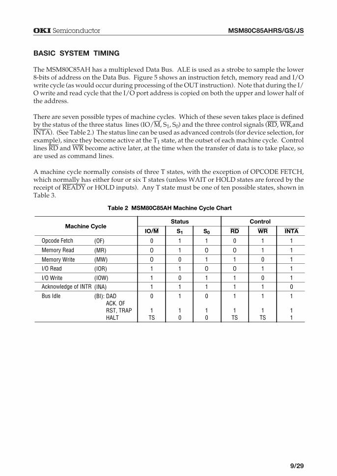
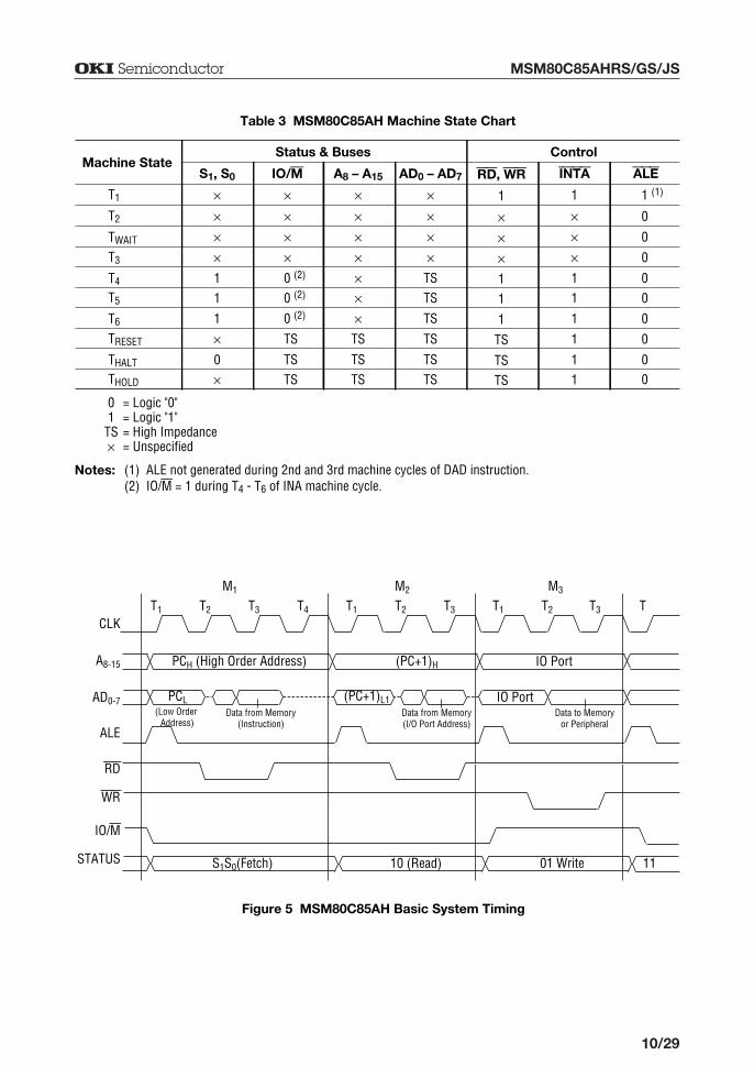
BASIC SYSTEM TIMING
The MSM80C85AH has a multiplexed Data Bus. ALE is used as a strobe to sample the lower8-bits of address on the Data Bus. Figure 5 shows an instruction fetch, memory read and I/Owrite cycle (as would occur during processing of the OUT instruction). Note that during the I/O write and read cycle that the I/O port address is copied on both the upper and lower half ofthe address.
There are seven possible types of machine cycles. Which of these seven takes place is definedby the status of the three status lines (IO/M, S1, S0) and the three control signals (RD, WR,andINTA). (See Table 2.) The status line can be used as advanced controls (for device selection, forexample), since they become active at the T1 state, at the outset of each machine cycle. Controllines RD and WR become active later, at the time when the transfer of data is to take place, soare used as command lines.
A machine cycle normally consists of three T states, with the exception of OPCODE FETCH,which normally has either four or six T states (unless WAIT or HOLD states are forced by thereceipt of READY or HOLD inputs). Any T state must be one of ten possible states, shown inTable 3.
Memory Read O
OMemory WriteI/O Read 1
1I/O Write
(MR)
Opcode Fetch 0(OF)
(MW)
(IOR)
Acknowledge of INTR 1(INA)(IOW)
Bus Idle 0
1TS
1
0
1
0
1
1
1
10
O
1
O
1
1
1
0
10
O
1
O
1
0
1
1
1TS
1
0
1
0
1
1
1
1TS
1
1
1
1
1
IO/M S1 S0 RD WR INTAMachine Cycle
Status Control
0
1
11
(BI): DAD ACK. OF RST, TRAP HALT
Table 2 MSM80C85AH Machine Cycle Chart
10/29
¡ Semiconductor MSM80C85AHRS/GS/JS
0
T2 ¥¥TWAIT
T3 ¥¥T4
T1 ¥
T5 ¥
¥¥¥
TS
¥
TS
¥¥¥1
1
1
¥¥¥1
1
1
0
0
0
0
1 (1)
0
A8 – A15 AD0 – AD7 RD, WR INTA ALEMachine State
Status & Buses Control
¥T6
TRESET TS
TSTHALT
THOLD TS
TS
TS
TSTS
1
TS
TSTS
1
1
11
0
0
0
¥¥¥1
¥
1
¥¥¥0 (2)
¥
0 (2)
S1, S0 IO/M
1
¥0¥
0 (2)
TS
TSTS
Table 3 MSM80C85AH Machine State Chart
0 = Logic "0"1 = Logic "1"
TS = High Impedance¥ = Unspecified
Notes: (1) ALE not generated during 2nd and 3rd machine cycles of DAD instruction.(2) IO/M = 1 during T4 - T6 of INA machine cycle.
T1
PCH (High Order Address) (PC+1)H A8-15
T2 T3 T4 T1 T2 T3 T1 T2
M3M2M1
T3 T
AD0-7
ALE
CLK
RD
WR
STATUS
IO/M
IO Port
IO PortPCL
S1S0(Fetch) 10 (Read) 01 Write 11
(Low Order Address)
Data from Memory(Instruction)
Data from Memory(I/O Port Address)
Data to Memoryor Peripheral
(PC+1)L1
Figure 5 MSM80C85AH Basic System Timing
11/29
¡ Semiconductor MSM80C85AHRS/GS/JS
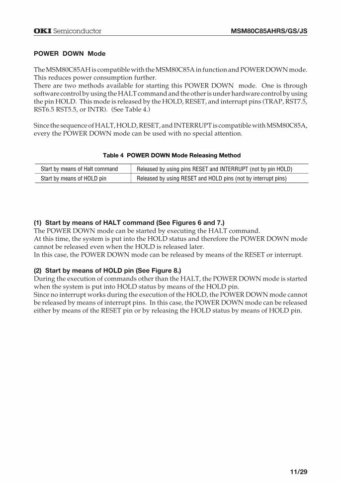
POWER DOWN Mode
The MSM80C85AH is compatible with the MSM80C85A in function and POWER DOWN mode.This reduces power consumption further.There are two methods available for starting this POWER DOWN mode. One is throughsoftware control by using the HALT command and the other is under hardware control by usingthe pin HOLD. This mode is released by the HOLD, RESET, and interrupt pins (TRAP, RST7.5,RST6.5 RST5.5, or INTR). (See Table 4.)
Since the sequence of HALT, HOLD, RESET, and INTERRUPT is compatible with MSM80C85A,every the POWER DOWN mode can be used with no special attention.
Start by means of Halt command
Start by means of HOLD pin
Released by using pins RESET and INTERRUPT (not by pin HOLD)
Released by using RESET and HOLD pins (not by interrupt pins)
Table 4 POWER DOWN Mode Releasing Method
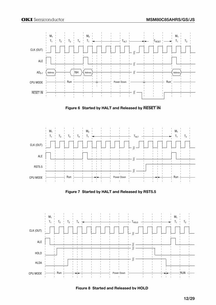
(1) Start by means of HALT command (See Figures 6 and 7.)The POWER DOWN mode can be started by executing the HALT command.At this time, the system is put into the HOLD status and therefore the POWER DOWN modecannot be released even when the HOLD is released later.In this case, the POWER DOWN mode can be released by means of the RESET or interrupt.
(2) Start by means of HOLD pin (See Figure 8.)During the execution of commands other than the HALT, the POWER DOWN mode is startedwhen the system is put into HOLD status by means of the HOLD pin.Since no interrupt works during the execution of the HOLD, the POWER DOWN mode cannotbe released by means of interrupt pins. In this case, the POWER DOWN mode can be releasedeither by means of the RESET pin or by releasing the HOLD status by means of HOLD pin.
12/29
¡ Semiconductor MSM80C85AHRS/GS/JS
T1
CLK (OUT)
ALE
Address
T2 T3 T4 T1
M1 M2
T1 T2
M1
THLT TRESET
Address AddressAD0-7
CPU MODE
RESET IN
Run Run
76H
Power Down
Figure 6 Started by HALT and Released by RESET IN
T1
CLK (OUT)
ALE
T2 T3 T4
M1
T1 T2
M1
THOLD
HOLD
CPU MODE Run RUN
HLDA
Power Down
Figure 8 Started and Released by HOLD
T1
CLK (OUT)
ALE
T2 T3 T4 T1
M1 M2
T1 T2
M1
THLT
CPU MODE
RST5.5
Run RunPower Down
Figure 7 Started by HALT and Released by RST5.5
13/29
¡ Semiconductor MSM80C85AHRS/GS/JS
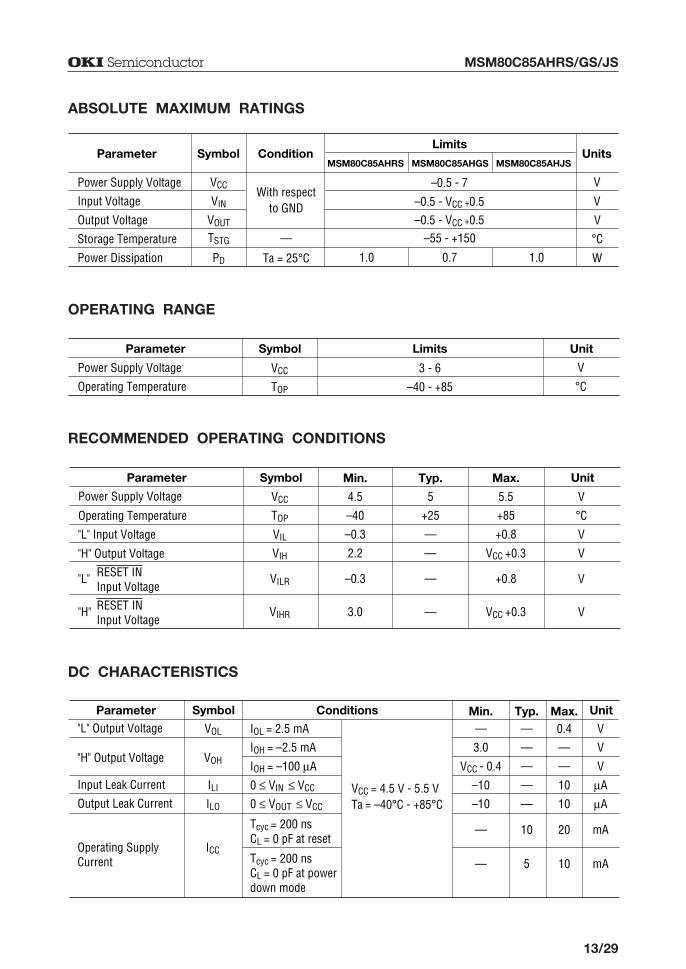
ABSOLUTE MAXIMUM RATINGS
–55 - +150
MSM80C85AHRS
Power Supply Voltage VCC –0.5 - 7 V
Input Voltage VIN –0.5 - VCC +0.5 V
Output Voltage VOUT –0.5 - VCC +0.5 V
Storage Temperature TSTG °C
Power Dissipation PD 0.7 W
Parameter UnitsSymbol
With respectto GND
—
Ta = 25°C
ConditionLimits
MSM80C85AHGS MSM80C85AHJS
1.01.0
OPERATING RANGE
Limits
Power Supply Voltage VCC 3 - 6 V
Operating Temperature TOP –40 - +85 °C
Parameter UnitSymbol
RECOMMENDED OPERATING CONDITIONS
DC CHARACTERISTICS
"L" VILR —–0.3 +0.8
Typ.
Power Supply Voltage VCC 5 V
TOP +25
"L" Input Voltage VIL —
"H" Output Voltage VIH —
Min.
4.5
–40
–0.3
2.2
Max.
5.5
+85
+0.8
VCC +0.3
Parameter UnitSymbol
°C
V
V
Operating Temperature
V
VIHR —3.0 VCC +0.3 V
RESET INInput Voltage
"H" RESET INInput Voltage
Typ. Max."L" Output Voltage VOL — 0.4 V
"H" Output Voltage VOH— — V
— — V
Parameter UnitSymbol Min.—
3.0
VCC - 0.4
IOL = 2.5 mA
IOH = –2.5 mA
IOH = –100 mA
Conditions
VCC = 4.5 V - 5.5 VTa = –40°C - +85°C
Input Leak Current ILI — 10 mA
Output Leak Current ILO — 10 mA
–10
–10
0 £ VIN £ VCC
0 £ VOUT £ VCC
Tcyc = 200 nsCL = 0 pF at reset
Operating SupplyCurrent
ICC
10 20 mA
5 10 mA
—
—Tcyc = 200 nsCL = 0 pF at power down mode
14/29
¡ Semiconductor MSM80C85AHRS/GS/JS
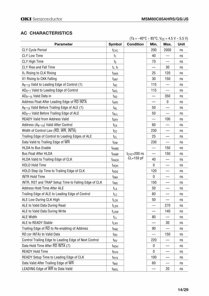
AC CHARACTERISTICS
Parameter Symbol Condition Min. Max. Unit
CLY Cycle Period tCYC
tCYC=200 ns CL=150 pF
200 2000 ns
CLY Low Time t1 40 — ns
CLY High Time t2 70 — ns
CLY Rise and Fall Time tr, tf — 30 ns
X1 Rising to CLK Rising tXKR 25 120 ns
X1 Rising to CKK Falling tXKF 30 150 ns
A8~15 Valid to Leading Edge of Control (1) tAC 115 — ns
AD0~7 Valid to Leading Edge of Control tACL 115 — ns
AD0~15 Valid Data in tAD — 350 ns
Address Float After Leading Edge of RD INTA tAFR — 0 ns
A8~15 Valid Before Trailing Edge of ALE (1) tAL 50 — ns
AD0~7 Valid Before Trailing Edge of ALE tALL 50 — ns
READY Valid from Address Valid tARY — 100 ns
Address (A8~15) Valid After Control tCA 60 — ns
Width of Control Law (RD, WR, INTA) tCC 230 — ns
Trailing Edge of Control to Leading Edges of ALE tCL 25 — ns
Data Valid to Trailing Edge of WR tDW 230 — ns
HLDA to Bus Enable tHABE — 150 ns
Bus Float After HLDA tHABF — 150 ns
HLDA Valid to Trailing Edge of CLK tHACK 40 — ns
HOLD Hold Time tHDH 0 — ns
HOLD Step Up Time to Trailing Edge of CLK tHDS 120 — ns
INTR Hold Time tINH 0 — ns
INTR, RST and TRAP Setup Time to Falling Edge of CLK tINS 150 — ns
Address Hold Time After ALE tLA 50 — ns
Trailing Edge of ALE to Leading Edge of Control tLC 60 — ns
ALE Low During CLK High tLCK 50 — ns
ALE to Valid Data During Read tLDR — 270 ns
ALE to Valid Data During Write tLDW — 140 ns
ALE Width tLL 80 — ns
ALE to READY Stable tLRY — 30 ns
Trailing Edge of RD to Re-enabling of Address tRAE 90 — ns
RD (or INTA) to Valid Data tRD — 150 ns
Control Trailing Edge to Leading Edge of Next Control tRV 220 — ns
Data Hold Time After RD INTA (7) tRDH 0 — ns
READY Hold Time tRYH 0 — ns
READY Setup Time to Leading Edge of CLK tRYS 100 — ns
Data Valid After Trailing Edge of WR tWD 60 — ns
LEADING Edge of WR to Data Vaild tWDL — 20 ns
(Ta = –40°C ~ 85°C, VCC = 4.5 V ~ 5.5 V)
15/29
¡ Semiconductor MSM80C85AHRS/GS/JS
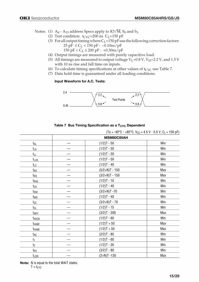
Notes: (1) A8 - A15 address Specs apply to IO/M, S0 and S1.(2) Test condition: tCYC=200 ns CL=150 pF(3) For all output timing where CL=150 pF use the following correction factors:
25 pF £ CL < 150 pF : –0.10ns/pF150 pF < CL £ 200 pF : +0.30ns/pF
(4) Output timings are measured with purely capacitive load.(5) All timings are measured to output voltage VL=0.8 V, VH=2.2 V, and 1.5 V
with 10 ns rise and fall time on inputs.(6) To calculate timing specifications at other values of tCYC use Table 7.(7) Data hold time is guaranteed under all loading conditions.
2.4
Test Points
2.2 2.2
0.8 0.80.45
Input Waveform for A.C. Tests:
(1/2)T - 50tAL Min
(Ta = -40°C - +85°C, VCC = 4.5 V - 5.5 V, CL = 150 pF)
(1/2)T - 50tLA Min
(1/2)T - 20tLL Min
(1/2)T - 50tLCK Min
(1/2)T - 40tLC Min
(5/2+N)T - 150tAD Max
(3/2+N)T - 150tRD Max
(1/2)T - 10tRAE Min
(1/2)T - 40tCA Min
(3/2+N)T -70tDW Min
(1/2)T - 40tWD Min
(3/2+N)T - 70tCC Min
(1/2)T - 75tCL Min
(3/2)T - 200tARY Max
(1/2)T - 60tHACK Min
(1/2)T + 50tHABF Max
(1/2)T + 50
(2/2)T - 85
tHABE Max
tAC Min
(1/2)T - 60t1 Min
(1/2)T - 30t2 Min
(3/2)T - 80tRV Min
tLDR Max
—
—
—
—
—
—
—
—
—
—
—
—
—
—
—
—
—
—
—
—
—
—
MSM80C85AH
Table 7 Bus Timing Specification as a TCYC Dependent
Note: N is equal to the total WAIT states.T = tCYC
(2+N)T -130
16/29
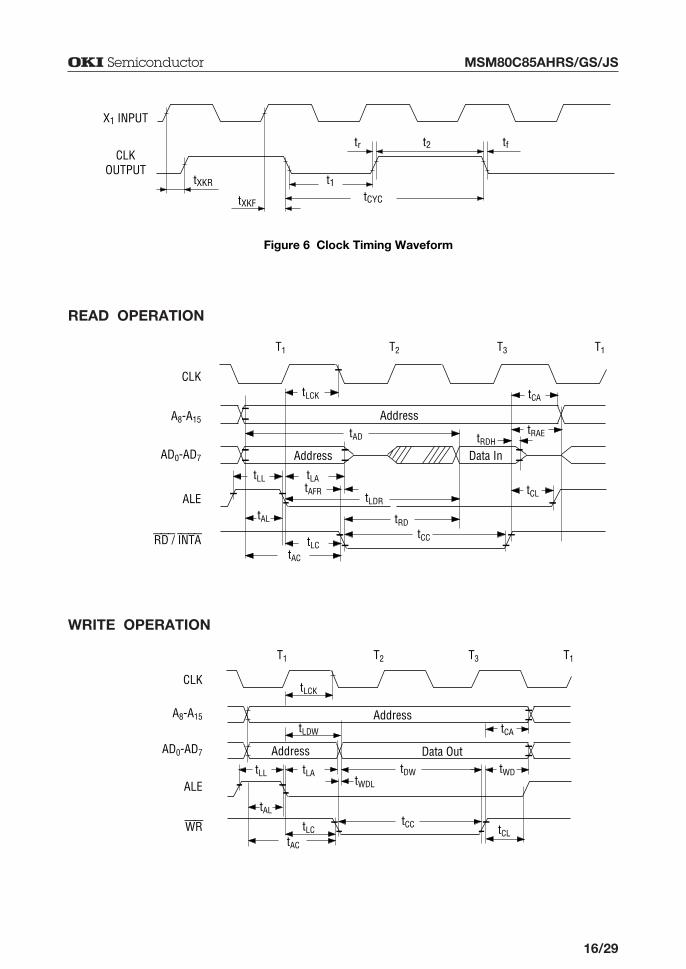
¡ Semiconductor MSM80C85AHRS/GS/JS
X1 INPUT
CLKOUTPUT
tXKR t1
tXKFtCYC
tr t2 tf
Figure 6 Clock Timing Waveform
READ OPERATION
CLK
A8-A15
AD0-AD7
ALE
RD / INTA
T1 T2 T3 T1
tLCK
tLL
tAL
Address
tAFR
tLCtAC
Address
tLA
tAD
tLDR
tRDtCC
tCA
tRAEtRDH
tCL
Data In
WRITE OPERATION
CLK
T1
tLDW
Address
tWDL
Data Out
A8-A15
AD0-AD7
ALE
WR
T2 T3 T1
Address
tLCK
tLA
tLC
tLL
tAL
tAC
tDW
tCC
tWD
tCL
tCA
17/29
¡ Semiconductor MSM80C85AHRS/GS/JS
CLK
A8~A15
AD0~AD7
ALE
RD / INTA
READY
T1 T2 TWAIT T3 T1
tLCK
tLL
tAL
Address
tAFR
tCLtACtARY
tLRY
tRYS tRYH
Address
tLA
tAD
tLDR
tRDtCC
tCA
tRAEtRDH
tCL
Data In
Note: READY must remain stable during setup and hold times.
Figure 7 MSM80C85AH Bus Timing, With and Without Wait
Read operation with Wait Cycle (Typical)–same READY timing applies to WRITE operation
CLK
T2
(Address, Controls)
tHDS
HOLD
HLDA
BUS
T3 THOLD THOLD T1
tHDH
tHABF
tHACK
tHABE
Figure 8 MSM80C85AH Hold Timing
HOLD OPERATION
18/29
¡ Semiconductor MSM80C85AHRS/GS/JS
T1
Call Inst
A8-15
tINS
T2 T4 T5 T6 THOLD T1 T2
AD0-7
ALE
RD
INTA
HOLD
HLDA
INTR
Bus Floating(1)
tINH
tHDS tHDH
tHACK tHABF
tHABE
NOTE: (1) IO/M is also floating during this time.
Figure 9 MSM80C85AH Interrupt and Hold Timing
19/29
¡ Semiconductor MSM80C85AHRS/GS/JS
MOVE, LOAD, AND STOREMOVr1 r2MOV M rMOV r MMVI rMVI MLXI BLXI DLXI HLXI SPSTAX BSTAX DLDAX BLDAX DSTALDASHLDLHLDXCHG
Mnemonic Description Instruction Code (1) Clock (2)Cycles
000000000000000001
111000000000000001
D1DD10011000011111
D1DD10101010111000
D0DD00000001101011
SS1110000000000000
SS1110000111111111
SS0001111000000001
D7 D6 D5 D4 D3 D2 D1 D0
4777
1010101010
7777
13131616
4
Move register to registerMove register to memoryMove memory to registerMove immediate registerMove immediate memoryLoad immediate register Pair B & CLoad immediate register Pair D & ELoad immediate register Pair H & LLoad immediate stack pointerStore A indirectStore A indirectLoad A indirectLoad A indirectStore A directLoad A directStore H & L directLoad H & L directExchange D & E H & L registers
STACK OPSPUSH BPUSH DPUSH HPUSH PSWPOP BPOP DPOP HPOP PSWXTHLSPHL
1111111111
1111111111
0011001111
0101010101
0000000001
1111000000
0000000010
1111111111
121212121010101016
6
Push register Pair B & C on stackPush register Pair D & E on stackPush register Pair H & L on stackPush A and Flags on stackPop register Pair B & C off stackPop register Pair D & E off stackPop register Pair H & L off stackPop A and Flags off stackExchange top of stack H & LH & L to stack pointer
JUMPJMPJCJNCJZJNZJPJMJPEJPOPCHL
1111111111
1111111111
0000011111
0110011000
0101001101
0000000000
1111111110
1000000001
107/107/107/107/107/107/107/107/10
6
Jump unconditionalJump on carryJump on no carryJump on zeroJump on no zeroJump on positiveJump on minusJump on parity evenJump on parity oddH & L to program counter
CALLCALLCCCNCCZCNZCPCMCPECPO
111111111
111111111
000001111
011001100
110100110
111111111
000000000
100000000
189/189/189/189/189/189/189/189/18
Call unconditionalCall on carryCall on no carryCall on zeroCall on no zeroCall on positiveCall on minusCall on parity evenCall on parity odd
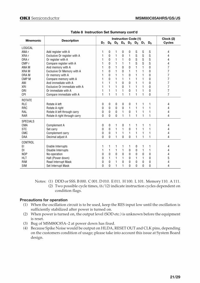
Table 8 Instruction Set Summary
20/29
¡ Semiconductor MSM80C85AHRS/GS/JS
RETURNRETRCRNCRZRNZRPRMRPERPO
Mnemonic Description Instruction Code (1) Clock (2)Cycles
111111111
111111111
000001111
011001100
110100110
000000000
000000000
100000000
D7 D6 D5 D4 D3 D2 D1 D0
106/126/126/126/126/126/126/126/12
Return Return on carryReturn on no carryReturn on zeroReturn on no zeroReturn on positiveReturn on minusReturn on parity evenReturn on parity odd
RESTARTRST 1 1 A A A 1 1 1 12Restart
INPUT/OUTPUTINOUT
11
11
00
11
10
00
11
11
1010
InputOutput
INCREMENT AND DECREMENTINR rDCR rINR MDCR MINX BINX DINX HINX SPDCX BDCX DDCX HDCX SP
000000000000
000000000000
DD1100110011
DD1101010101
DD0000001111
111100000000
000011111111
010111111111
44
101066666666
Increment registerDecrement registerIncrement memoryDecrement memoryIncrement B & C registersIncrement D & E registersIncrement H & L registersIncrement stack pointerDecrement B & CDecrement D & EDecrement H & LDecrement stack pointer
ADDADD rADC rADD MADC MADIACIDAD BDAD DDAD HDAD SP
1111110000
0000110000
0000000011
0000000101
0101011111
SS11110000
SS11110000
SS00001111
447777
10101010
Add register to AAdd register to A with carryAdd memory to AAdd memory to A with carryAdd immediate to AAdd immediate to A with carryAdd B & C to H & LAdd D & E to H & LAdd H & L to H & LAdd stack pointer to H & L
SUBTRACTSUB rSBB rSUB MSBB MSUISBI
111111
000011
000000
111111
010101
SS1111
SS1111
SS0000
447777
Subtract register from A Subtract register from A with borrowSubtract memory from ASubtract memory from A with borrowSubtract immediate from ASubtract immediate from A with borrow
Table 8 Instruction Set Summary cont'd
21/29
¡ Semiconductor MSM80C85AHRS/GS/JS
LOGICALANA rXRA rORA rCMP rANA MXRA MORA MCMP MANI XRIORICPI
Mnemonic Description Instruction Code (1) Clock (2)Cycles
111111111111
000000001111
111111111111
001100110011
010101010101
SSSS11111111
SSSS11111111
SSSS00000000
D7 D6 D5 D4 D3 D2 D1 D0
444477777777
Add register with AExclusive Or register with AOr register with ACompare register with AAnd memory with AExclusive Or Memory with AOr memory with ACompare memory with AAnd immediate with AExclusive Or immediate with AOr immediate with ACompare immediate with A
ROTATERLCRRCRALRAR
0000
0000
0000
0011
0101
1111
1111
1111
4444
Rotate A leftRotate A right Rotate A left through carryRotate A right through carry
SPECIALSCMASTCCMCDAA
0000
0000
1111
0110
1010
1111
1111
1111
4444
Complement ASet carryComplement carryDecimal adjust A
CONTROLEIDINOPHLTRIMSIM
110000
110100
110111
110101
100000
000100
110100
110000
444544
Enable InterruptsDisable InterruptsNo-operationHalt (Power down)Read Interrupt MaskSet Interrupt Mask
Table 8 Instruction Set Summary cont'd
Notes: (1) DDD or SSS. B 000. C 001. D 010. E 011. H 100. L 101. Memory 110. A 111.(2) Two possible cycle times, (6/12) indicate instruction cycles dependent on
condition flags.
Precautions for operation(1) When the oscillation circuit is to be used, keep the RES input low until the oscillation is
sufficiently stabilized after power is turned on.(2) When power is turned on, the output level (SOD etc.) is unknown before the equipment
is reset.(3) Bug of MSM80C85A–2 at power down has fixed.(4) Because Spike Noise would be output on HLDA, RESET OUT and CLK pins, depending
on the customers condition of usage; please take into account this issue at System Boarddesign.
22/29
¡ Semiconductor MSM80C85AHRS/GS/JS
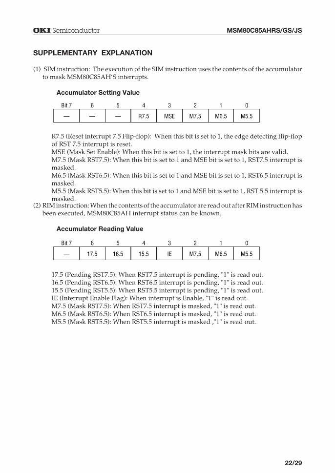
SUPPLEMENTARY EXPLANATION
(1) SIM instruction: The execution of the SIM instruction uses the contents of the accumulatorto mask MSM80C85AH’S interrupts.
Accumulator Setting Value
R7.5 (Reset interrupt 7.5 Flip-flop): When this bit is set to 1, the edge detecting flip-flopof RST 7.5 interrupt is reset.MSE (Mask Set Enable): When this bit is set to 1, the interrupt mask bits are valid.M7.5 (Mask RST7.5): When this bit is set to 1 and MSE bit is set to 1, RST7.5 interrupt ismasked.M6.5 (Mask RST6.5): When this bit is set to 1 and MSE bit is set to 1, RST6.5 interrupt ismasked.M5.5 (Mask RST5.5): When this bit is set to 1 and MSE bit is set to 1, RST 5.5 interrupt ismasked.
—
Bit 7
—
6
—
5
R7.5
4
MSE
3
M7.5
2
M6.5
1
M5.5
0
(2) RIM instruction: When the contents of the accumulator are read out after RIM instruction hasbeen executed, MSM80C85AH interrupt status can be known.
Accumulator Reading Value
—
Bit 7
17.5
6
16.5
5
15.5
4
IE
3
M7.5
2
M6.5
1
M5.5
0
17.5 (Pending RST7.5): When RST7.5 interrupt is pending, "1" is read out.16.5 (Pending RST6.5): When RST6.5 interrupt is pending, "1" is read out.15.5 (Pending RST5.5): When RST5.5 interrupt is pending, "1" is read out.IE (Interrupt Enable Flag): When interrupt is Enable, "1" is read out.M7.5 (Mask RST7.5): When RST7.5 interrupt is masked, "1" is read out.M6.5 (Mask RST6.5): When RST6.5 interrupt is masked, "1" is read out.M5.5 (Mask RST5.5): When RST5.5 interrupt is masked ,"1" is read out.
23/29
¡ Semiconductor MSM80C85AHRS/GS/JS
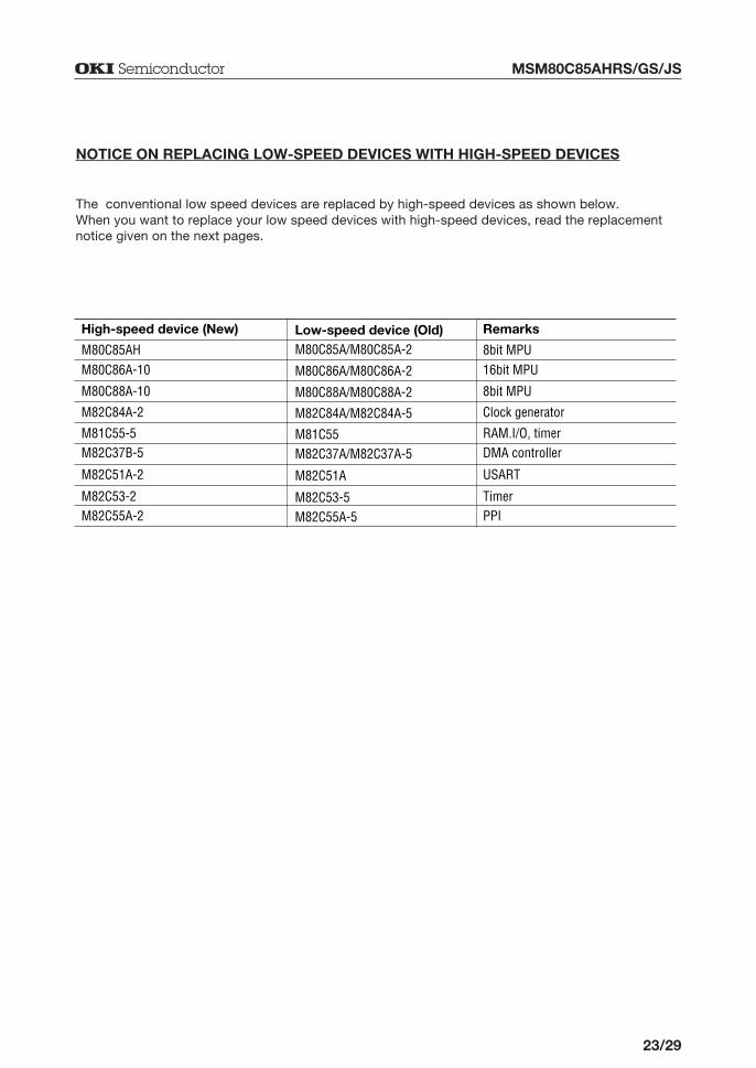
NOTICE ON REPLACING LOW-SPEED DEVICES WITH HIGH-SPEED DEVICES
The conventional low speed devices are replaced by high-speed devices as shown below.When you want to replace your low speed devices with high-speed devices, read the replacementnotice given on the next pages.
High-speed device (New) Low-speed device (Old) Remarks
M80C85AH M80C85A/M80C85A-2 8bit MPUM80C86A-10 M80C86A/M80C86A-2 16bit MPU
M80C88A-10 M80C88A/M80C88A-2 8bit MPU
M82C84A-2 M82C84A/M82C84A-5 Clock generator
M81C55-5 M81C55 RAM.I/O, timerM82C37B-5 M82C37A/M82C37A-5 DMA controller
M82C51A-2 M82C51A USART
M82C53-2 M82C53-5 TimerM82C55A-2 M82C55A-5 PPI
24/29
¡ Semiconductor MSM80C85AHRS/GS/JS
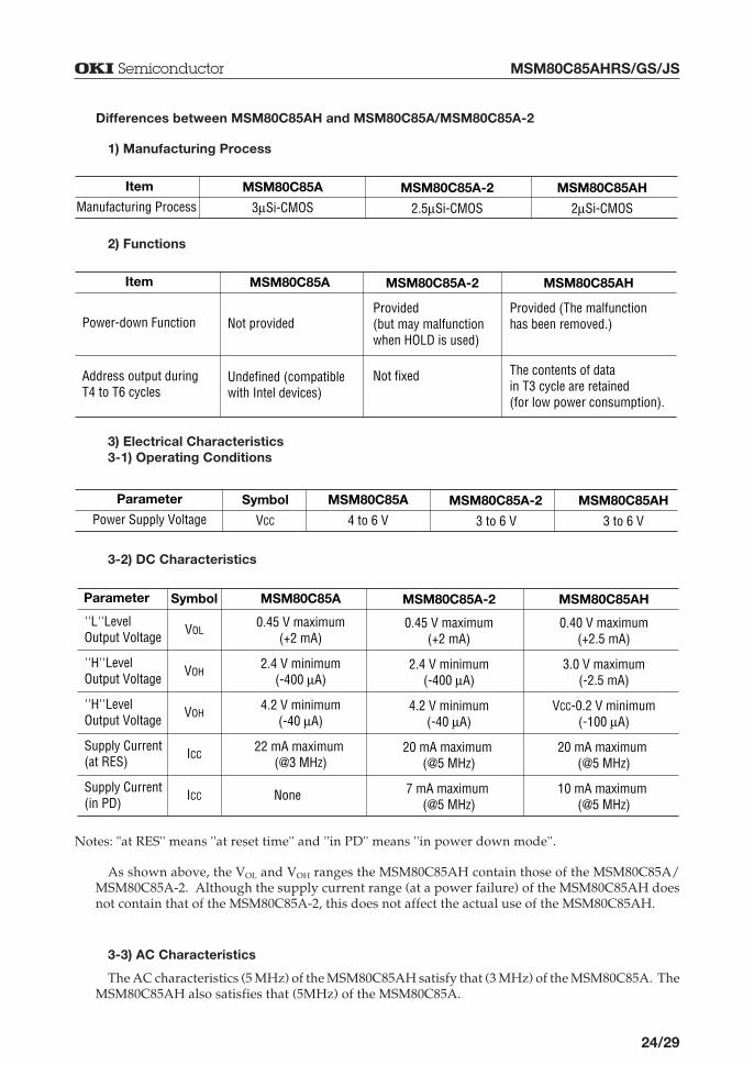
Differences between MSM80C85AH and MSM80C85A/MSM80C85A-2
1) Manufacturing Process
2) Functions
3) Electrical Characteristics3-1) Operating Conditions
3-2) DC Characteristics
Item MSM80C85A MSM80C85A-2 MSM80C85AHManufacturing Process 3mSi-CMOS 2.5mSi-CMOS 2mSi-CMOS
Notes: "at RES'' means ''at reset time'' and ''in PD'' means ''in power down mode''.
As shown above, the VOL and VOH ranges the MSM80C85AH contain those of the MSM80C85A/MSM80C85A-2. Although the supply current range (at a power failure) of the MSM80C85AH doesnot contain that of the MSM80C85A-2, this does not affect the actual use of the MSM80C85AH.
3-3) AC Characteristics
The AC characteristics (5 MHz) of the MSM80C85AH satisfy that (3 MHz) of the MSM80C85A. TheMSM80C85AH also satisfies that (5MHz) of the MSM80C85A.
Parameter MSM80C85A MSM80C85A-2 MSM80C85AHPower Supply Voltage 4 to 6 V 3 to 6 V 3 to 6 V
Symbol
VCC
Item MSM80C85A MSM80C85A-2 MSM80C85AH
Power-down Function Not providedProvided (but may malfunction when HOLD is used)
Provided (The malfunctionhas been removed.)
Address output during T4 to T6 cycles
Undefined (compatiblewith Intel devices)
Not fixed The contents of data in T3 cycle are retained(for low power consumption).
Parameter MSM80C85A MSM80C85A-2 MSM80C85AH
''L''Level Output Voltage
0.45 V maximum(+2 mA)
0.45 V maximum(+2 mA)
0.40 V maximum(+2.5 mA)
Symbol
VOL
''H''LevelOutput Voltage
2.4 V minimum(-400 mA)
2.4 V minimum(-400 mA)
3.0 V maximum(-2.5 mA)
VOH
''H''LevelOutput Voltage
4.2 V minimum(-40 mA)
4.2 V minimum(-40 mA)
VCC-0.2 V minimum(-100 mA)
VOH
Supply Current (at RES)
22 mA maximum (@3 MHz)
20 mA maximum (@5 MHz)
20 mA maximum (@5 MHz)
ICC
Supply Current (in PD)
None 7 mA maximum (@5 MHz)
10 mA maximum (@5 MHz)
ICC
25/29
¡ Semiconductor MSM80C85AHRS/GS/JS
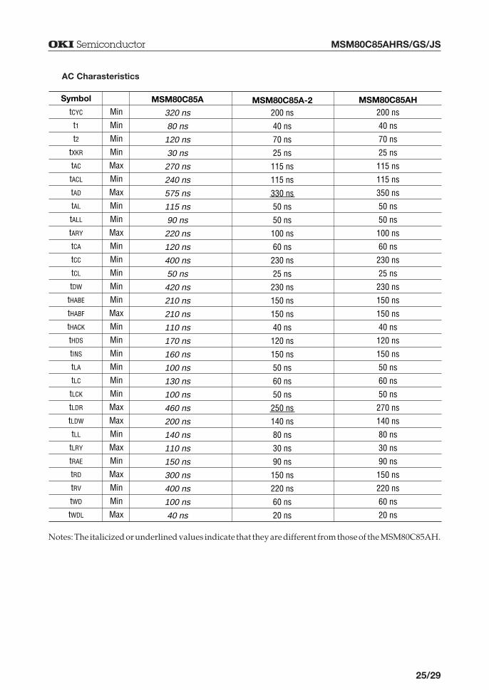
AC Charasteristics
Notes: The italicized or underlined values indicate that they are different from those of the MSM80C85AH.
MSM80C85ASymbol MSM80C85A-2 MSM80C85AH
320 nstCYC 200 ns 200 ns
80 nst1 40 ns 40 ns
120 nst2 70 ns 70 ns
30 nstXKR 25 ns 25 ns
270 nstAC 115 ns 115 ns
240 nstACL 115 ns 115 ns
575 nstAD 350 ns
115 nstAL 50 ns 50 ns
90 nstALL 50 ns 50 ns
220 nstARY 100 ns 100 ns
120 nstCA 60 ns 60 ns
400 nstCC 230 ns 230 ns
50 nstCL 25 ns 25 ns
420 nstDW 230 ns 230 ns
210 nstHABE 150 ns 150 ns
210 nstHABF 150 ns 150 ns
110 nstHACK 40 ns 40 ns
170 nstHDS 120 ns 120 ns
160 nstINS 150 ns 150 ns
100 nstLA 50 ns 50 ns
130 nstLC 60 ns 60 ns
100 nstLCK 50 ns 50 ns
460 nstLDR 270 ns
200 nstLDW 140 ns 140 ns
140 nstLL 80 ns 80 ns
110 nstLRY 30 ns 30 ns
150 nstRAE 90 ns 90 ns
300 nstRD 150 ns 150 ns
400 nstRV 220 ns 220 ns
100 nstWD 60 ns 60 ns
40 nstWDL 20 ns 20 ns
Min
Min
Min
Min
Max
Min
Max
Min
Min
Max
Min
Min
Min
Min
Min
Max
Min
Min
Min
Min
Min
Min
Max
Max
Min
Max
Min
Max
Min
Max
Min
330 ns
250 ns
26/29
¡ Semiconductor MSM80C85AHRS/GS/JS
4) Other notes
1) As the MSM80C85AH employs the 2 m process, its noise characteristics may be a little different fromthose of the MSM80C85A. When devices are replaced for upgrading, it is recommended to performnoise evaluation. Especially, HLDA, RESOUT, and CLKOUT pins must be evaluated.
2) The MSM80C85AH basically satisfies the characteristics of the MSM80C85A-2 and the MSM80C85A,but their timings are a little different, Therefore, when critical timing is required in designing, it isrecommended to evaluate operating margins at various temperatures and voltages.
27/29
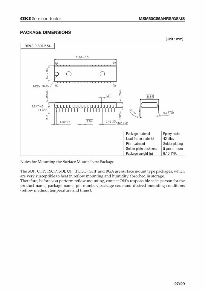
¡ Semiconductor MSM80C85AHRS/GS/JS
(Unit : mm)
PACKAGE DIMENSIONS
Notes for Mounting the Surface Mount Type Package
The SOP, QFP, TSOP, SOJ, QFJ (PLCC), SHP and BGA are surface mount type packages, whichare very susceptible to heat in reflow mounting and humidity absorbed in storage.Therefore, before you perform reflow mounting, contact Oki’s responsible sales person for theproduct name, package name, pin number, package code and desired mounting conditions(reflow method, temperature and times).
DIP40-P-600-2.54
Package materialLead frame materialPin treatmentSolder plate thicknessPackage weight (g)
Epoxy resin42 alloySolder plating5 mm or more6.10 TYP.
28/29
¡ Semiconductor MSM80C85AHRS/GS/JS
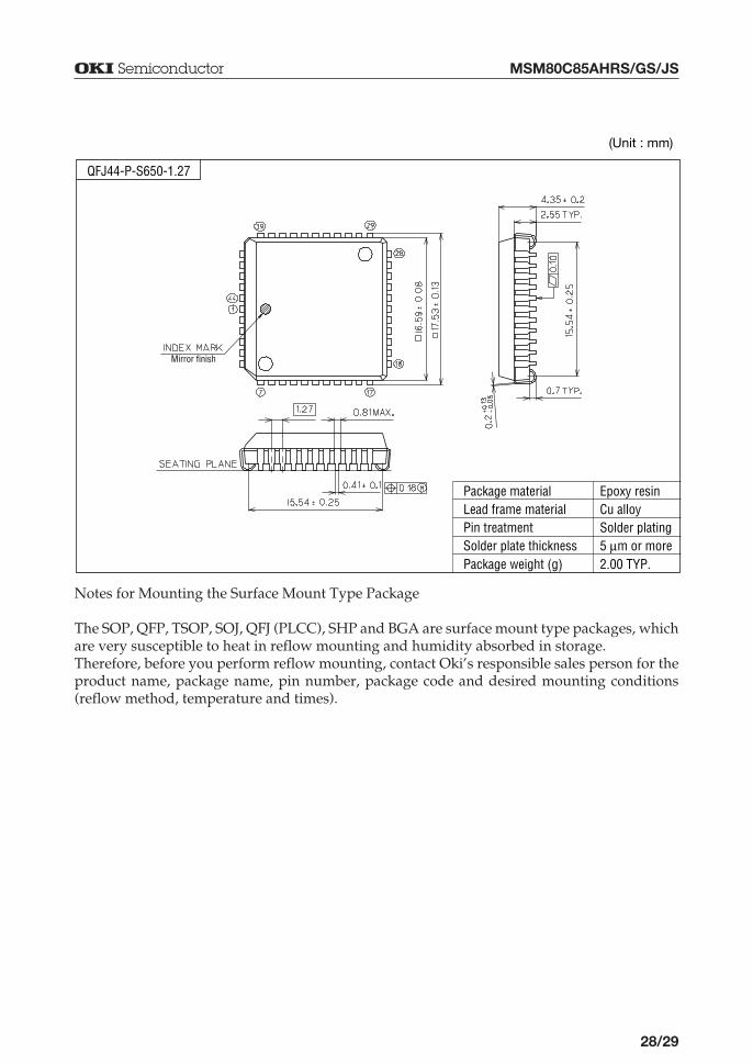
(Unit : mm)
Notes for Mounting the Surface Mount Type Package
The SOP, QFP, TSOP, SOJ, QFJ (PLCC), SHP and BGA are surface mount type packages, whichare very susceptible to heat in reflow mounting and humidity absorbed in storage.Therefore, before you perform reflow mounting, contact Oki’s responsible sales person for theproduct name, package name, pin number, package code and desired mounting conditions(reflow method, temperature and times).
QFJ44-P-S650-1.27
Package materialLead frame materialPin treatmentSolder plate thicknessPackage weight (g)
Epoxy resinCu alloySolder plating5 mm or more2.00 TYP.
Mirror finish
29/29
¡ Semiconductor MSM80C85AHRS/GS/JS
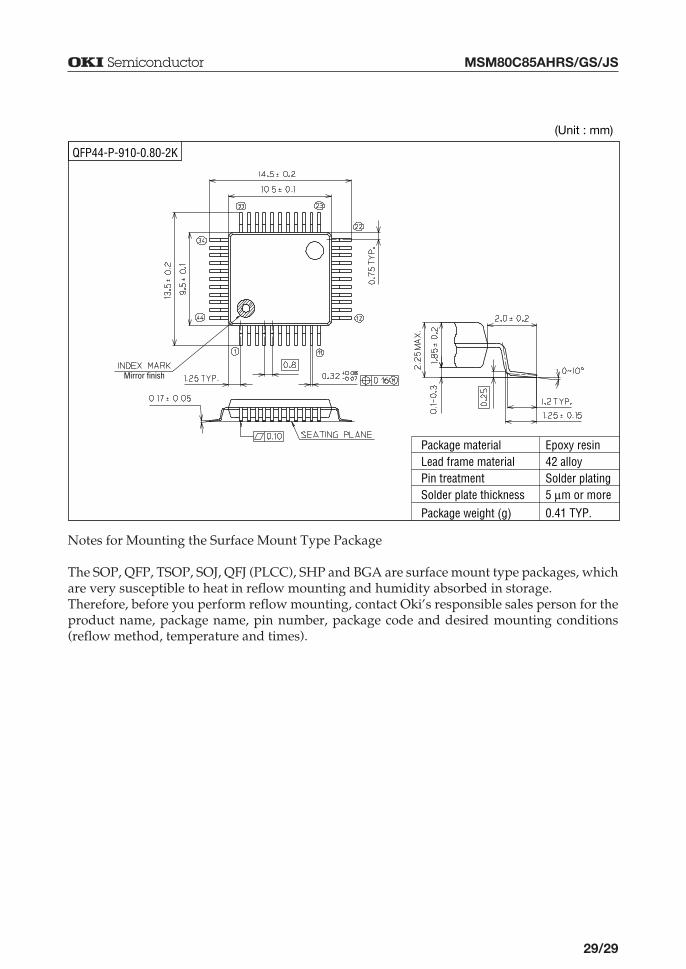
(Unit : mm)
Notes for Mounting the Surface Mount Type Package
The SOP, QFP, TSOP, SOJ, QFJ (PLCC), SHP and BGA are surface mount type packages, whichare very susceptible to heat in reflow mounting and humidity absorbed in storage.Therefore, before you perform reflow mounting, contact Oki’s responsible sales person for theproduct name, package name, pin number, package code and desired mounting conditions(reflow method, temperature and times).
Package materialLead frame materialPin treatmentSolder plate thickness
Package weight (g)
Epoxy resin42 alloySolder plating5 mm or more
0.41 TYP.
QFP44-P-910-0.80-2K
Mirror finish