Embed Size (px)
Citation preview

The content and copyrights of the attached material are the property of its owner.
Distributed by:
www.Jameco.com 1-800-831-4242
1/27December 2005
M48T08M48T08Y, M48T18
5V, 64 Kbit (8 Kb x8) TIMEKEEPER® SRAM
Rev 7.0
FEATURES SUMMARY INTEGRATED ULTRA LOW POWER SRAM,
REAL TIME CLOCK, POWER-FAIL CONTROL CIRCUIT, AND BATTERY
BYTEWIDE™ RAM-LIKE CLOCK ACCESS BCD CODED YEAR, MONTH, DAY, DATE,
HOURS, MINUTES, and SECONDS TYPICAL CLOCK ACCURACY OF ±1
MINUTE A MONTH, AT 25°C AUTOMATIC POWER-FAIL CHIP
DESELECT AND WRITE PROTECTION WRITE PROTECT VOLTAGES
(VPFD = Power-fail Deselect Voltage):– M48T08: VCC = 4.75 to 5.5V
4.5V ≤ VPFD ≤ 4.75V– M48T18/T08Y: VCC = 4.5 to 5.5V
4.2V ≤ VPFD ≤ 4.5V SOFTWARE CONTROLLED CLOCK
CALIBRATION FOR HIGH ACCURACY APPLICATIONS
SELF-CONTAINED BATTERY AND CRYSTAL IN THE CAPHAT™ DIP PACKAGE
PACKAGING INCLUDES A 28-LEAD SOIC AND SNAPHAT® TOP (to be ordered separately)
SOIC PACKAGE PROVIDES DIRECT CONNECTION FOR A SNAPHAT TOP WHICH CONTAINS THE BATTERY AND CRYSTAL
PIN AND FUNCTION COMPATIBLE WITH DS1643 and JEDEC STANDARD 8K x8 SRAMs
RoHS COMPLIANCELead-free components are compliant with the RoHS Directive.
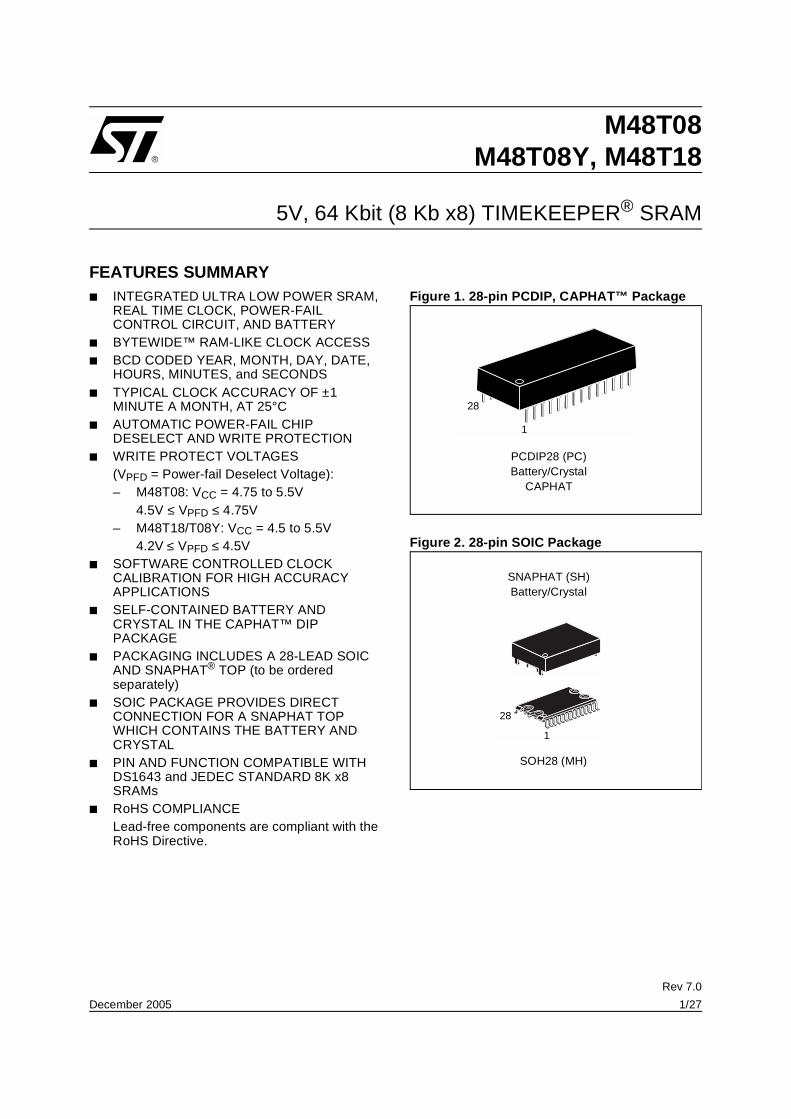
Figure 1. 28-pin PCDIP, CAPHAT™ Package
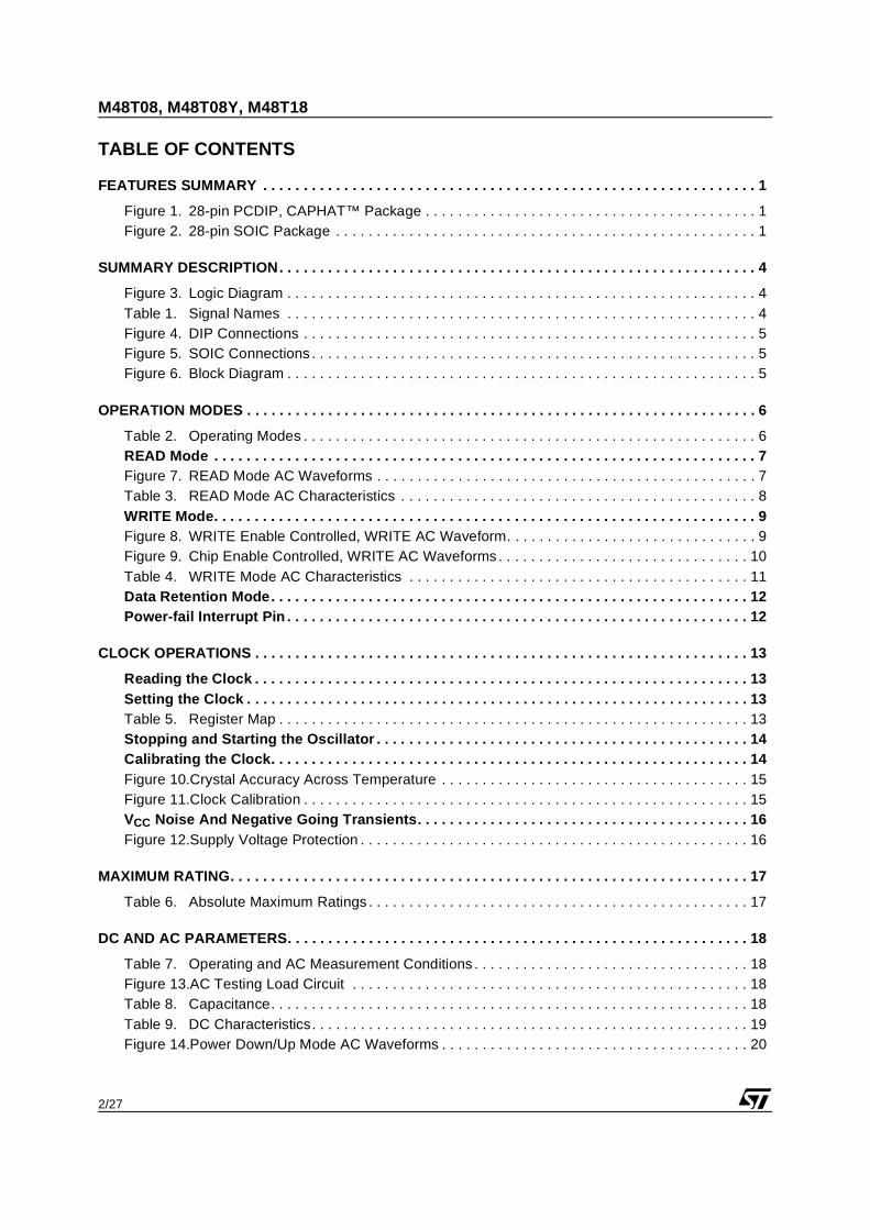
Figure 2. 28-pin SOIC Package
28
1
PCDIP28 (PC)Battery/Crystal
CAPHAT
28
1
SNAPHAT (SH)Battery/Crystal
SOH28 (MH)
M48T08, M48T08Y, M48T18
2/27
TABLE OF CONTENTS
FEATURES SUMMARY . . . . . . . . . . . . . . . . . . . . . . . . . . . . . . . . . . . . . . . . . . . . . . . . . . . . . . . . . . . . . 1
Figure 1. 28-pin PCDIP, CAPHAT™ Package . . . . . . . . . . . . . . . . . . . . . . . . . . . . . . . . . . . . . . . . . 1Figure 2. 28-pin SOIC Package . . . . . . . . . . . . . . . . . . . . . . . . . . . . . . . . . . . . . . . . . . . . . . . . . . . . 1
SUMMARY DESCRIPTION. . . . . . . . . . . . . . . . . . . . . . . . . . . . . . . . . . . . . . . . . . . . . . . . . . . . . . . . . . . 4
Figure 3. Logic Diagram . . . . . . . . . . . . . . . . . . . . . . . . . . . . . . . . . . . . . . . . . . . . . . . . . . . . . . . . . . 4Table 1. Signal Names . . . . . . . . . . . . . . . . . . . . . . . . . . . . . . . . . . . . . . . . . . . . . . . . . . . . . . . . . . 4Figure 4. DIP Connections . . . . . . . . . . . . . . . . . . . . . . . . . . . . . . . . . . . . . . . . . . . . . . . . . . . . . . . . 5Figure 5. SOIC Connections . . . . . . . . . . . . . . . . . . . . . . . . . . . . . . . . . . . . . . . . . . . . . . . . . . . . . . . 5Figure 6. Block Diagram . . . . . . . . . . . . . . . . . . . . . . . . . . . . . . . . . . . . . . . . . . . . . . . . . . . . . . . . . . 5
OPERATION MODES . . . . . . . . . . . . . . . . . . . . . . . . . . . . . . . . . . . . . . . . . . . . . . . . . . . . . . . . . . . . . . . 6
Table 2. Operating Modes . . . . . . . . . . . . . . . . . . . . . . . . . . . . . . . . . . . . . . . . . . . . . . . . . . . . . . . . 6READ Mode . . . . . . . . . . . . . . . . . . . . . . . . . . . . . . . . . . . . . . . . . . . . . . . . . . . . . . . . . . . . . . . . . . . 7Figure 7. READ Mode AC Waveforms . . . . . . . . . . . . . . . . . . . . . . . . . . . . . . . . . . . . . . . . . . . . . . . 7Table 3. READ Mode AC Characteristics . . . . . . . . . . . . . . . . . . . . . . . . . . . . . . . . . . . . . . . . . . . . 8WRITE Mode. . . . . . . . . . . . . . . . . . . . . . . . . . . . . . . . . . . . . . . . . . . . . . . . . . . . . . . . . . . . . . . . . . . 9Figure 8. WRITE Enable Controlled, WRITE AC Waveform. . . . . . . . . . . . . . . . . . . . . . . . . . . . . . . 9Figure 9. Chip Enable Controlled, WRITE AC Waveforms . . . . . . . . . . . . . . . . . . . . . . . . . . . . . . . 10Table 4. WRITE Mode AC Characteristics . . . . . . . . . . . . . . . . . . . . . . . . . . . . . . . . . . . . . . . . . . 11Data Retention Mode. . . . . . . . . . . . . . . . . . . . . . . . . . . . . . . . . . . . . . . . . . . . . . . . . . . . . . . . . . . 12Power-fail Interrupt Pin . . . . . . . . . . . . . . . . . . . . . . . . . . . . . . . . . . . . . . . . . . . . . . . . . . . . . . . . . 12
CLOCK OPERATIONS . . . . . . . . . . . . . . . . . . . . . . . . . . . . . . . . . . . . . . . . . . . . . . . . . . . . . . . . . . . . . 13
Reading the Clock . . . . . . . . . . . . . . . . . . . . . . . . . . . . . . . . . . . . . . . . . . . . . . . . . . . . . . . . . . . . . 13Setting the Clock . . . . . . . . . . . . . . . . . . . . . . . . . . . . . . . . . . . . . . . . . . . . . . . . . . . . . . . . . . . . . . 13Table 5. Register Map . . . . . . . . . . . . . . . . . . . . . . . . . . . . . . . . . . . . . . . . . . . . . . . . . . . . . . . . . . 13Stopping and Starting the Oscillator . . . . . . . . . . . . . . . . . . . . . . . . . . . . . . . . . . . . . . . . . . . . . . 14Calibrating the Clock. . . . . . . . . . . . . . . . . . . . . . . . . . . . . . . . . . . . . . . . . . . . . . . . . . . . . . . . . . . 14Figure 10.Crystal Accuracy Across Temperature . . . . . . . . . . . . . . . . . . . . . . . . . . . . . . . . . . . . . . 15Figure 11.Clock Calibration . . . . . . . . . . . . . . . . . . . . . . . . . . . . . . . . . . . . . . . . . . . . . . . . . . . . . . . 15VCC Noise And Negative Going Transients. . . . . . . . . . . . . . . . . . . . . . . . . . . . . . . . . . . . . . . . . 16Figure 12.Supply Voltage Protection . . . . . . . . . . . . . . . . . . . . . . . . . . . . . . . . . . . . . . . . . . . . . . . . 16
MAXIMUM RATING. . . . . . . . . . . . . . . . . . . . . . . . . . . . . . . . . . . . . . . . . . . . . . . . . . . . . . . . . . . . . . . . 17
Table 6. Absolute Maximum Ratings . . . . . . . . . . . . . . . . . . . . . . . . . . . . . . . . . . . . . . . . . . . . . . . 17
DC AND AC PARAMETERS. . . . . . . . . . . . . . . . . . . . . . . . . . . . . . . . . . . . . . . . . . . . . . . . . . . . . . . . . 18
Table 7. Operating and AC Measurement Conditions . . . . . . . . . . . . . . . . . . . . . . . . . . . . . . . . . . 18Figure 13.AC Testing Load Circuit . . . . . . . . . . . . . . . . . . . . . . . . . . . . . . . . . . . . . . . . . . . . . . . . . 18Table 8. Capacitance. . . . . . . . . . . . . . . . . . . . . . . . . . . . . . . . . . . . . . . . . . . . . . . . . . . . . . . . . . . 18Table 9. DC Characteristics. . . . . . . . . . . . . . . . . . . . . . . . . . . . . . . . . . . . . . . . . . . . . . . . . . . . . . 19Figure 14.Power Down/Up Mode AC Waveforms . . . . . . . . . . . . . . . . . . . . . . . . . . . . . . . . . . . . . . 20
3/27
M48T08, M48T08Y, M48T18
Table 10. Power Down/Up AC Characteristics . . . . . . . . . . . . . . . . . . . . . . . . . . . . . . . . . . . . . . . . 20Table 11. Power Down/Up Trip Points DC Characteristics . . . . . . . . . . . . . . . . . . . . . . . . . . . . . . . 20
PACKAGE MECHANICAL INFORMATION . . . . . . . . . . . . . . . . . . . . . . . . . . . . . . . . . . . . . . . . . . . . . 21
Figure 15.PCDIP28 – 28-pin Plastic DIP, battery CAPHAT, Package Outline . . . . . . . . . . . . . . . . 21Table 12. PCDIP28 – 28-pin Plastic DIP, battery CAPHAT, Package Mechanical Data. . . . . . . . . 21Figure 16.SOH28 – 28-lead Plastic Small Outline, 4-socket battery SNAPHAT, Package Outline. 22Table 13. SOH28 – 28-lead Plastic SO, 4-socket battery SNAPHAT, Package Mech. Data . . . . . 22Figure 17.SH – 4-pin SNAPHAT Housing for 48mAh Battery & Crystal, Package Outline . . . . . . . 23Table 14. SH – 4-pin SNAPHAT Housing for 48mAh Battery & Crystal, Package Mech. Data. . . . 23Figure 18.SH – 4-pin SNAPHAT Housing for 120mAh Battery & Crystal, Package Outline . . . . . . 24Table 15. SH – 4-pin SNAPHAT Housing for 120mAh Battery & Crystal, Package Mech. Data. . . 24
PART NUMBERING . . . . . . . . . . . . . . . . . . . . . . . . . . . . . . . . . . . . . . . . . . . . . . . . . . . . . . . . . . . . . . . 25
Table 16. Ordering Information Scheme . . . . . . . . . . . . . . . . . . . . . . . . . . . . . . . . . . . . . . . . . . . . . 25Table 17. SNAPHAT Battery Table . . . . . . . . . . . . . . . . . . . . . . . . . . . . . . . . . . . . . . . . . . . . . . . . . 25
REVISION HISTORY. . . . . . . . . . . . . . . . . . . . . . . . . . . . . . . . . . . . . . . . . . . . . . . . . . . . . . . . . . . . . . . 26
Table 18. Document Revision History . . . . . . . . . . . . . . . . . . . . . . . . . . . . . . . . . . . . . . . . . . . . . . . 26
M48T08, M48T08Y, M48T18
4/27
SUMMARY DESCRIPTIONThe M48T08/18/08Y TIMEKEEPER® RAM is an8K x 8 non-volatile static RAM and real time clockwhich is pin and functional compatible with theDS1643. The monolithic chip is available in twospecial packages to provide a highly integratedbattery backed-up memory and real time clock so-lution.The M48T08/18/08Y is a non-volatile pin and func-tion equivalent to any JEDEC standard 8K x 8SRAM. It also easily fits into many ROM, EPROM,and EEPROM sockets, providing the non-volatilityof PROMs without any requirement for specialWRITE timing or limitations on the number ofWRITEs that can be performed.The 28-pin, 600mil DIP CAPHAT™ houses theM48T08/18/08Y silicon with a quartz crystal and along- life lithium button cell in a single package.
The 28-pin, 330mil SOIC provides sockets withgold plated contacts at both ends for direct con-nection to a separate SNAPHAT® housing con-taining the battery and crystal. The unique designallows the SNAPHAT battery package to bemounted on top of the SOIC package after thecompletion of the surface mount process. Inser-tion of the SNAPHAT housing after reflow pre-vents potential battery and crystal damage due tothe high temperatures required for device surface-mounting. The SNAPHAT housing is keyed to pre-vent reverse insertion.The SOIC and battery/crystal packages areshipped separately in plastic anti-static tubes or inTape & Reel form. For the 28 lead SOIC, the bat-tery/crystal package (e.g., SNAPHAT) part num-ber is “M4T28-BR12SH” or “M4T32-BR12SH”(see Table 17., page 25).
Figure 3. Logic Diagram Table 1. Signal Names
AI01020
13
A0-A12
W
DQ0-DQ7
VCC
M48T08M48T08YM48T18
G
E2
VSS
8
E1 INT
A0-A12 Address Inputs
DQ0-DQ7 Data Inputs / Outputs
INT Power Fail Interrupt (Open Drain)
E1 Chip Enable 1
E2 Chip Enable 2
G Output Enable
W WRITE Enable
VCC Supply Voltage
VSS Ground
5/27
M48T08, M48T08Y, M48T18
Figure 4. DIP Connections Figure 5. SOIC Connections
Figure 6. Block Diagram
A1A0
DQ0
A7
A4A3A2
A6A5
E2
A10
A8A9
DQ7
W
A11G
E1
DQ5DQ1DQ2
DQ3VSS
DQ4
DQ6
A12INT VCC
AI01182
M48T08M48T188
1234567
91011121314
1615
282726252423222120191817
AI01021B
8
234567
91011121314
2221201918171615
282726252423
1
A1A0
DQ0
A7
A4A3A2
A6A5
E2
A10
A8A9
DQ7
W
A11G
E1
DQ5DQ1DQ2
DQ3VSS
DQ4
DQ6
A12INT VCC
M48T08Y
AI01333
LITHIUMCELL
OSCILLATOR ANDCLOCK CHAIN
VPFD
INTVCC VSS
32,768 HzCRYSTAL
VOLTAGE SENSEAND
SWITCHINGCIRCUITRY
8 x 8 BiPORTSRAM ARRAY
8184 x 8SRAM ARRAY
A0-A12
DQ0-DQ7
E1
E2
W
G
POWER
M48T08, M48T08Y, M48T18
6/27
OPERATION MODESAs Figure 6., page 5 shows, the static memory ar-ray and the quartz-controlled clock oscillator of theM48T08/18/08Y are integrated on one silicon chip.The two circuits are interconnected at the uppereight memory locations to provide user accessibleBYTEWIDE™ clock information in the bytes withaddresses 1FF8h-1FFFh.The clock locations contain the year, month, date,day, hour, minute, and second in 24 hour BCD for-mat. Corrections for 28, 29 (leap year - valid until2100), 30, and 31 day months are made automat-ically. Byte 1FF8h is the clock control register. Thisbyte controls user access to the clock informationand also stores the clock calibration setting.The eight clock bytes are not the actual clockcounters themselves; they are memory locationsconsisting of BiPORT™ READ/WRITE memory
cells. The M48T08/18/08Y includes a clock controlcircuit which updates the clock bytes with currentinformation once per second. The information canbe accessed by the user in the same manner asany other location in the static memory array.The M48T08/18/08Y also has its own Power-failDetect circuit. The control circuitry constantly mon-itors the single 5V supply for an out of tolerancecondition. When VCC is out of tolerance, the circuitwrite protects the SRAM, providing a high degreeof data security in the midst of unpredictable sys-tem operation brought on by low VCC. As VCC fallsbelow the Battery Back-up Switchover Voltage(VSO), the control circuitry connects the batterywhich maintains data and clock operation until val-id power returns.
Table 2. Operating Modes
Note: X = VIH or VIL; VSO = Battery Back-up Switchover Voltage.1. See Table 11., page 20 for details.
Mode VCC E1 E2 G W DQ0-DQ7 Power
Deselect
4.75 to 5.5Vor
4.5 to 5.5V
VIH X X X High Z Standby
Deselect X VIL X X High Z Standby
WRITE VIL VIH X VIL DIN Active
READ VIL VIH VIL VIH DOUT Active
READ VIL VIH VIH VIH High Z Active
Deselect VSO to VPFD(min)(1) X X X X High Z CMOS Standby
Deselect ≤ VSO(1) X X X X High Z Battery Back-up Mode
7/27
M48T08, M48T08Y, M48T18
READ Mode
The M48T08/18/08Y is in the READ Mode when-ever W (WRITE Enable) is high, E1 (Chip Enable1) is low, and E2 (Chip Enable 2) is high. The de-vice architecture allows ripple-through access ofdata from eight of 65,536 locations in the staticstorage array. Thus, the unique address specifiedby the 13 address inputs defines which one of the8,192 bytes of data is to be accessed. Valid datawill be available at the Data I/O pins within addressaccess time (tAVQV) after the last address inputsignal is stable, providing that the E1, E2, and Gaccess times are also satisfied. If the E1, E2 andG access times are not met, valid data will be
available after the latter of the Chip Enable Accesstimes (tE1LQV or tE2HQV) or Output Enable Accesstime (tGLQV).The state of the eight three-state Data I/O signalsis controlled by E1, E2 and G. If the outputs are ac-tivated before tAVQV, the data lines will be driven toan indeterminate state until tAVQV. If the addressinputs are changed while E1, E2 and G remain ac-tive, output data will remain valid for Output DataHold time (tAXQX) but will go indeterminate until thenext address access.
Figure 7. READ Mode AC Waveforms
Note: WRITE Enable (W) = High.
AI00962
tAVAV
tAVQV tAXQX
tE1LQV
tE1LQX
tE1HQZ
tGLQV
tGLQX
tGHQZ
VALID
A0-A12
E1
G
DQ0-DQ7
tE2HQV
tE2HQX
VALID
tE2LQZ
E2
M48T08, M48T08Y, M48T18
8/27
Table 3. READ Mode AC Characteristics
Note: 1. Valid for Ambient Operating Temperature: TA = 0 to 70°C; VCC = 4.75 to 5.5V or 4.5 to 5.5V (except where noted).
Symbol Parameter(1)
M48T08/M48T18/T08Y
Unit–100/–10 (T08Y) –150/–15 (T08Y)
Min Max Min Max
tAVAV READ Cycle Time 100 150 ns
tAVQV Address Valid to Output Valid 100 150 ns
tE1LQV Chip Enable 1 Low to Output Valid 100 150 ns
tE2HQV Chip Enable 2 High to Output Valid 100 150 ns
tGLQV Output Enable Low to Output Valid 50 75 ns
tE1LQX Chip Enable 1 Low to Output Transition 10 10 ns
tE2HQX Chip Enable 2 High to Output Transition 10 10 ns
tGLQX Output Enable Low to Output Transition 5 5 ns
tE1HQZ Chip Enable 1 High to Output Hi-Z 50 75 ns
tE2LQZ Chip Enable 2 Low to Output Hi-Z 50 75 ns
tGHQZ Output Enable High to Output Hi-Z 40 60 ns
tAXQX Address Transition to Output Transition 5 5 ns
9/27
M48T08, M48T08Y, M48T18
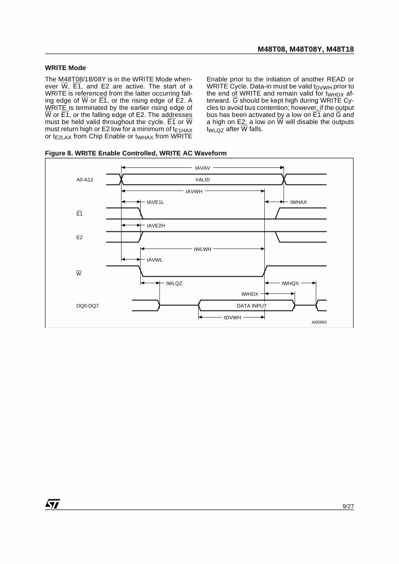
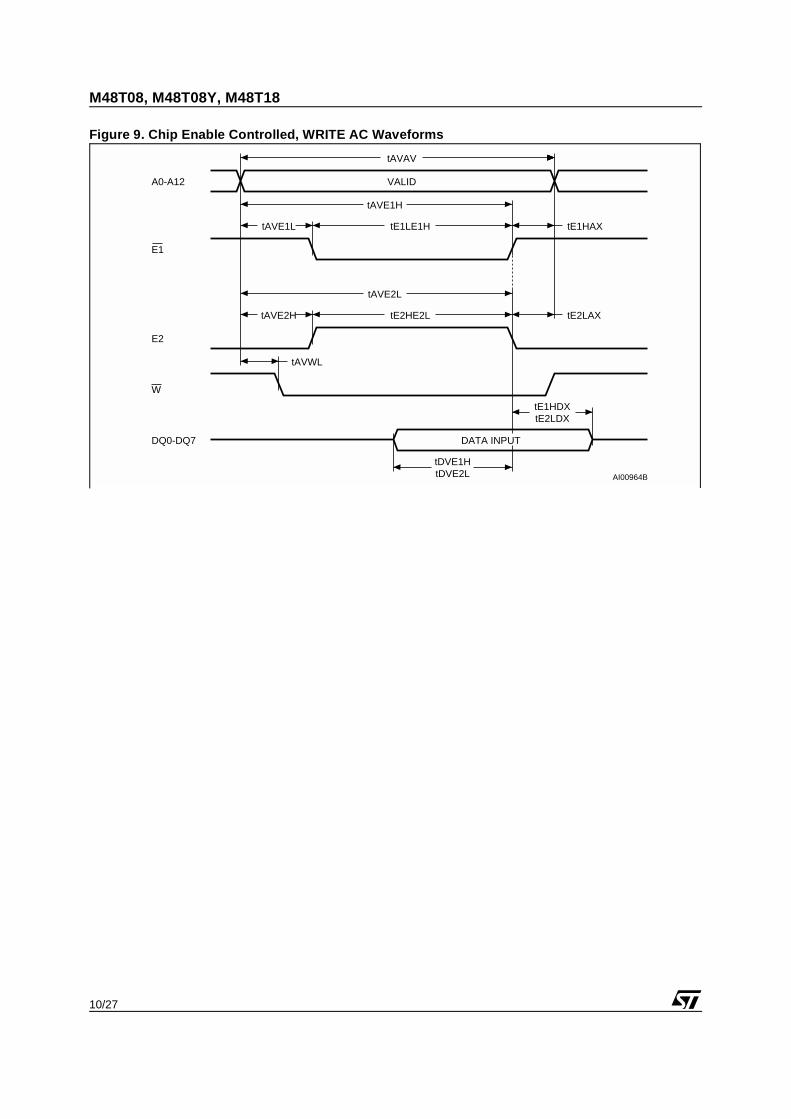
WRITE Mode
The M48T08/18/08Y is in the WRITE Mode when-ever W, E1, and E2 are active. The start of aWRITE is referenced from the latter occurring fall-ing edge of W or E1, or the rising edge of E2. AWRITE is terminated by the earlier rising edge ofW or E1, or the falling edge of E2. The addressesmust be held valid throughout the cycle. E1 or Wmust return high or E2 low for a minimum of tE1HAXor tE2LAX from Chip Enable or tWHAX from WRITE
Enable prior to the initiation of another READ orWRITE Cycle. Data-in must be valid tDVWH prior tothe end of WRITE and remain valid for tWHDX af-terward. G should be kept high during WRITE Cy-cles to avoid bus contention; however, if the outputbus has been activated by a low on E1 and G anda high on E2, a low on W will disable the outputstWLQZ after W falls.
Figure 8. WRITE Enable Controlled, WRITE AC Waveform
AI00963
tAVAV
tWHAX
tDVWH
DATA INPUT
A0-A12
E1
W
DQ0-DQ7
VALID
E2
tAVWH
tAVE1L
tAVE2H
tWLWH
tAVWL
tWLQZ
tWHDX
tWHQX
M48T08, M48T08Y, M48T18
10/27
Figure 9. Chip Enable Controlled, WRITE AC Waveforms
AI00964B
tAVAV
tE1HAX
tDVE1HtDVE2L
A0-A12
E1
W
DQ0-DQ7
VALID
E2
tAVE1H
tAVE1L
tAVWL
tAVE2L
tE1LE1H
tE2LAXtAVE2H tE2HE2L
tE1HDXtE2LDX
DATA INPUT
11/27
M48T08, M48T08Y, M48T18
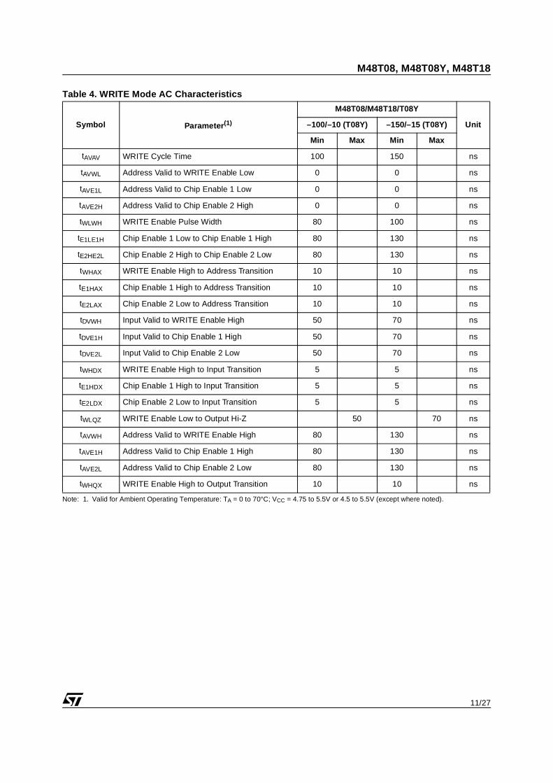
Table 4. WRITE Mode AC Characteristics
Note: 1. Valid for Ambient Operating Temperature: TA = 0 to 70°C; VCC = 4.75 to 5.5V or 4.5 to 5.5V (except where noted).
Symbol Parameter(1)
M48T08/M48T18/T08Y
Unit–100/–10 (T08Y) –150/–15 (T08Y)
Min Max Min Max
tAVAV WRITE Cycle Time 100 150 ns
tAVWL Address Valid to WRITE Enable Low 0 0 ns
tAVE1L Address Valid to Chip Enable 1 Low 0 0 ns
tAVE2H Address Valid to Chip Enable 2 High 0 0 ns
tWLWH WRITE Enable Pulse Width 80 100 ns
tE1LE1H Chip Enable 1 Low to Chip Enable 1 High 80 130 ns
tE2HE2L Chip Enable 2 High to Chip Enable 2 Low 80 130 ns
tWHAX WRITE Enable High to Address Transition 10 10 ns
tE1HAX Chip Enable 1 High to Address Transition 10 10 ns
tE2LAX Chip Enable 2 Low to Address Transition 10 10 ns
tDVWH Input Valid to WRITE Enable High 50 70 ns
tDVE1H Input Valid to Chip Enable 1 High 50 70 ns
tDVE2L Input Valid to Chip Enable 2 Low 50 70 ns
tWHDX WRITE Enable High to Input Transition 5 5 ns
tE1HDX Chip Enable 1 High to Input Transition 5 5 ns
tE2LDX Chip Enable 2 Low to Input Transition 5 5 ns
tWLQZ WRITE Enable Low to Output Hi-Z 50 70 ns
tAVWH Address Valid to WRITE Enable High 80 130 ns
tAVE1H Address Valid to Chip Enable 1 High 80 130 ns
tAVE2L Address Valid to Chip Enable 2 Low 80 130 ns
tWHQX WRITE Enable High to Output Transition 10 10 ns
M48T08, M48T08Y, M48T18
12/27
Data Retention Mode
With valid VCC applied, the M48T08/18/08Y oper-ates as a conventional BYTEWIDE™ static RAM.Should the supply voltage decay, the RAM will au-tomatically power-fail deselect, write protecting it-self when VCC falls within the VPFD (max), VPFD(min) window. All outputs become high imped-ance, and all inputs are treated as “Don't care.”Note: A power failure during a WRITE cycle maycorrupt data at the currently addressed location,but does not jeopardize the rest of the RAM's con-tent. At voltages below VPFD (min), the user can beassured the memory will be in a write protectedstate, provided the VCC fall time is not less than tF.The M48T08/18/08Y may respond to transientnoise spikes on VCC that reach into the deselectwindow during the time the device is samplingVCC. Therefore, decoupling of the power supplylines is recommended.When VCC drops below VSO, the control circuitswitches power to the internal battery which pre-serves data and powers the clock. The internalbutton cell will maintain data in the M48T08/18/08Y for an accumulated period of at least 10 yearswhen VCC is less than VSO.
Note: Requires use of M4T32-BR12SHSNAPHAT® top when using the SOH28 package.As system power returns and VCC rises aboveVSO, the battery is disconnected and the powersupply is switched to external VCC.Write protection continues until VCC reaches VPFD(min) plus trec (min). E1 should be kept high or E2low as VCC rises past VPFD (min) to prevent inad-vertent WRITE cycles prior to system stabilization.Normal RAM operation can resume trec after VCCexceeds VPFD (max).For more information on Battery Storage Life referto the Application Note AN1012.
Power-fail Interrupt Pin
The M48T08/18/08Y continuously monitors VCC.When VCC falls to the power-fail detect trip point,an interrupt is immediately generated. An internalclock provides a delay of between 10µs and 40µsbefore automatically deselecting the M48T08/18/08Y. The INT pin is an open drain output and re-quires an external pull up resistor, even if the inter-rupt output function is not being used.
13/27
M48T08, M48T08Y, M48T18
CLOCK OPERATIONS
Reading the Clock
Updates to the TIMEKEEPER® registers shouldbe halted before clock data is read to preventreading data in transition. The BiPORT™ TIME-KEEPER cells in the RAM array are only data reg-isters and not the actual clock counters, soupdating the registers can be halted without dis-turbing the clock itself.Updating is halted when a '1' is written to theREAD Bit, the seventh bit in the control register.As long as a '1' remains in that position, updatingis halted. After a halt is issued, the registers reflectthe count; that is, the day, date, and the time thatwere current at the moment the halt command wasissued.All of the TIMEKEEPER registers are updated si-multaneously. A halt will not interrupt an update inprogress. Updating is within a second after the bitis reset to a '0.'
Setting the Clock
The eighth bit of the control register is the WRITEBit. Setting the WRITE Bit to a '1,' like the READBit, halts updates to the TIMEKEEPER registers.The user can then load them with the correct day,date, and time data in 24 hour BCD format (on Ta-ble 5.). Resetting the WRITE Bit to a '0' then trans-fers the values of all time registers (1FF9h-1FFFh)to the actual TIMEKEEPER counters and allowsnormal operation to resume. The FT Bit and thebits marked as '0' in Table 5. must be written to '0'to allow for normal TIMEKEEPER and RAM oper-ation.See the Application Note AN923, “TIMEKEEPER®
Rolling Into the 21st Century” for information onCentury Rollover.
Table 5. Register Map
Keys: S = SIGN BitFT = FREQUENCY TEST Bit (Set to '0' for normal clock operation)R = READ BitW = WRITE BitST = STOP Bit0 = Must be set to '0'
Address Data Function/Range
BCD FormatD7 D6 D5 D4 D3 D2 D1 D0
1FFFh 10 Years Year Year 00-99
1FFEh 0 0 0 10 M Month Month 01-12
1FFDh 0 0 10 Date Date Date 01-31
1FFCh 0 FT 0 0 0 Day Day 01-07
1FFBh 0 0 10 Hours Hours Hours 00-23
1FFAh 0 10 Minutes Minutes Minutes 00-59
1FF9h ST 10 Seconds Seconds Seconds 00-59
1FF8h W R S Calibration Control
M48T08, M48T08Y, M48T18
14/27
Stopping and Starting the Oscillator
The oscillator may be stopped at any time. If thedevice is going to spend a significant amount oftime on the shelf, the oscillator can be turned off tominimize current drain on the battery. The STOPBit (ST) is the MSB of the seconds register. Settingit to a '1' stops the oscillator. The M48T08/18/08Y(in the PCDIP28 package) is shipped from STMi-croelectronics with the STOP Bit set to a '1.' Whenreset to a '0,' the M48T08/18/08Y oscillator startswithin one second.Note: To guarantee oscillator start-up after initialpower-up, first write the STOP Bit (ST) to '1,' thenreset to '0.'
Calibrating the Clock
The M48T08/18/08Y is driven by a quartz-con-trolled oscillator with a nominal frequency of32,768 Hz. A typical M48T08/18/08Y is accuratewithin 1 minute per month at 25°C without calibra-tion. The devices are tested not to exceed ± 35ppm (parts per million) oscillator frequency error at25°C, which equates to about ±1.53 minutes permonth. With the calibration bits properly set, theaccuracy of each M48T08/18/08Y improves tobetter than +1/–2 ppm at 25°C.The oscillation rate of any crystal changes withtemperature. Figure 10., page 15 shows the fre-quency error that can be expected at various tem-peratures. Most clock chips compensate forcrystal frequency and temperature shift error withcumbersome “trim” capacitors. The M48T08/18/08Y design, however, employs periodic countercorrection. The calibration circuit adds or subtractscounts from the oscillator divider circuit at the di-vide by 256 stage, as shown in Figure11., page 15. The number of times pulses areblanked (subtracted, negative calibration) or split(added, positive calibration) depends upon thevalue loaded into the five-bit Calibration Bytefound in the Control Register. Adding countsspeeds the clock up, subtracting counts slows theclock down.The Calibration Byte occupies the five lower orderbits in the Control register. This byte can be set torepresent any value between 0 and 31 in binaryform. The sixth bit is the Sign Bit; '1' indicates pos-itive calibration, '0' indicates negative calibration.Calibration occurs within a 64 minute cycle. Thefirst 62 minutes in the cycle may, once per minute,have one second either shortened by 128 or
lengthened by 256 oscillator cycles. If a binary '1'is loaded into the register, only the first 2 minutesin the 64 minute cycle will be modified; if a binary6 is loaded, the first 12 will be affected, and so on.Therefore, each calibration step has the effect ofadding 512 or subtracting 256 oscillator cycles forevery 125,829,120 actual oscillator cycles; that is+4.068 or –2.034 ppm of adjustment per calibra-tion step in the calibration register. Assuming thatthe oscillator is in fact running at exactly 32,768Hz,each of the 31 increments in the Calibration Bytewould represent +10.7 or –5.35 seconds permonth which corresponds to a total range of +5.5or –2.75 minutes per month.Two methods are available for ascertaining howmuch calibration a given M48T08/18/08Y may re-quire. The first involves simply setting the clock,letting it run for a month and comparing it to aknown accurate reference (like WWV broadcasts).While that may seem crude, it allows the designerto give the end user the ability to calibrate his clockas his environment may require, even after the fi-nal product is packaged in a non-user serviceableenclosure. All the designer has to do is provide asimple utility that accesses the Calibration Byte.The second approach is better suited to a manu-facturing environment, and involves the use ofstandard test equipment. When the FrequencyTest (FT) Bit, the seventh-most significant bit inthe Day Register, is set to a '1,' and the oscillatoris running at 32,768 Hz, the LSB (DQ0) of the Sec-onds Register will toggle at 512 Hz. Any deviationfrom 512 Hz indicates the degree and direction ofoscillator frequency shift at the test temperature.For example, a reading of 512.01024 Hz would in-dicate a +20 ppm oscillator frequency error, requir-ing a –10 (WR001010) to be loaded into theCalibration Byte for correction.Note: Setting or changing the Calibration Bytedoes not affect the Frequency Test output fre-quency. The device must be selected and ad-dresses must be stable at Address 1FF9h whenreading the 512 Hz on DQ0.The LSB of the Seconds Register is monitored byholding the M48T08/18/08Y in an extended READof the Seconds Register, but without having theREAD Bit set. The FT Bit MUST be reset to '0' fornormal clock operations to resume.For more information on calibration, see the Appli-cation Note AN934, “TIMEKEEPER® Calibration.”
15/27
M48T08, M48T08Y, M48T18
Figure 10. Crystal Accuracy Across Temperature
Figure 11. Clock Calibration
AI02124
-80
-60
-100
-40
-20
0
20
0 5 10 15 20 25 30 35 40 45 50 55 60 65 70
∆F = -0.038 (T - T0)2 ± 10%
FppmC2
T0 = 25 °C
ppm
°C
AI00594B
NORMAL
POSITIVECALIBRATION
NEGATIVECALIBRATION
M48T08, M48T08Y, M48T18
16/27
VCC Noise And Negative Going Transients
ICC transients, including those produced by outputswitching, can produce voltage fluctuations, re-sulting in spikes on the VCC bus. These transientscan be reduced if capacitors are used to store en-ergy which stabilizes the VCC bus. The energystored in the bypass capacitors will be released aslow going spikes are generated or energy will beabsorbed when overshoots occur. A ceramic by-pass capacitor value of 0.1µF (as shown in Figure12.) is recommended in order to provide the need-ed filtering.In addition to transients that are caused by normalSRAM operation, power cycling can generate neg-ative voltage spikes on VCC that drive it to valuesbelow VSS by as much as one volt. These negativespikes can cause data corruption in the SRAMwhile in battery backup mode. To protect fromthese voltage spikes, it is recommended to con-nect a schottky diode from VCC to VSS (cathodeconnected to VCC, anode to VSS). Schottky diode1N5817 is recommended for through hole andMBRS120T3 is recommended for surface mount.
Figure 12. Supply Voltage Protection
AI02169
VCC
0.1µF DEVICE
VCC
VSS
17/27
M48T08, M48T08Y, M48T18
MAXIMUM RATINGStressing the device above the rating listed in the“Absolute Maximum Ratings” table may causepermanent damage to the device. These arestress ratings only and operation of the device atthese or any other conditions above those indicat-ed in the Operating sections of this specification is
not implied. Exposure to Absolute Maximum Rat-ing conditions for extended periods may affect de-vice reliability. Refer also to theSTMicroelectronics SURE Program and other rel-evant quality documents.
Table 6. Absolute Maximum Ratings
Note: 1. For DIP package: Soldering temperature not to exceed 260°C for 10 seconds (total thermal budget not to exceed 150°C for longerthan 30 seconds).
2. For SO package, standard (SnPb) lead finish: Reflow at peak temperature of 225°C (total thermal budget not to exceed 180°C forbetween 90 to 150 seconds).
3. For SO package, Lead-free (Pb-free) lead finish: Reflow at peak temperature of 260°C (total thermal budget not to exceed 245°Cfor greater than 30 seconds).
CAUTION: Negative undershoots below –0.3V are not allowed on any pin while in the Battery Back-up mode.CAUTION: Do NOT wave solder SOIC to avoid damaging SNAPHAT sockets.
Symbol Parameter Value Unit
TA Ambient Operating Temperature 0 to 70 °C
TSTG Storage Temperature (VCC Off, Oscillator Off) –40 to 85 °C
TSLD(1,2,3) Lead Solder Temperature for 10 seconds 260 °C
VIO Input or Output Voltages –0.3 to 7 V
VCC Supply Voltage –0.3 to 7 V
IO Output Current 20 mA
PD Power Dissipation 1 W
M48T08, M48T08Y, M48T18
18/27
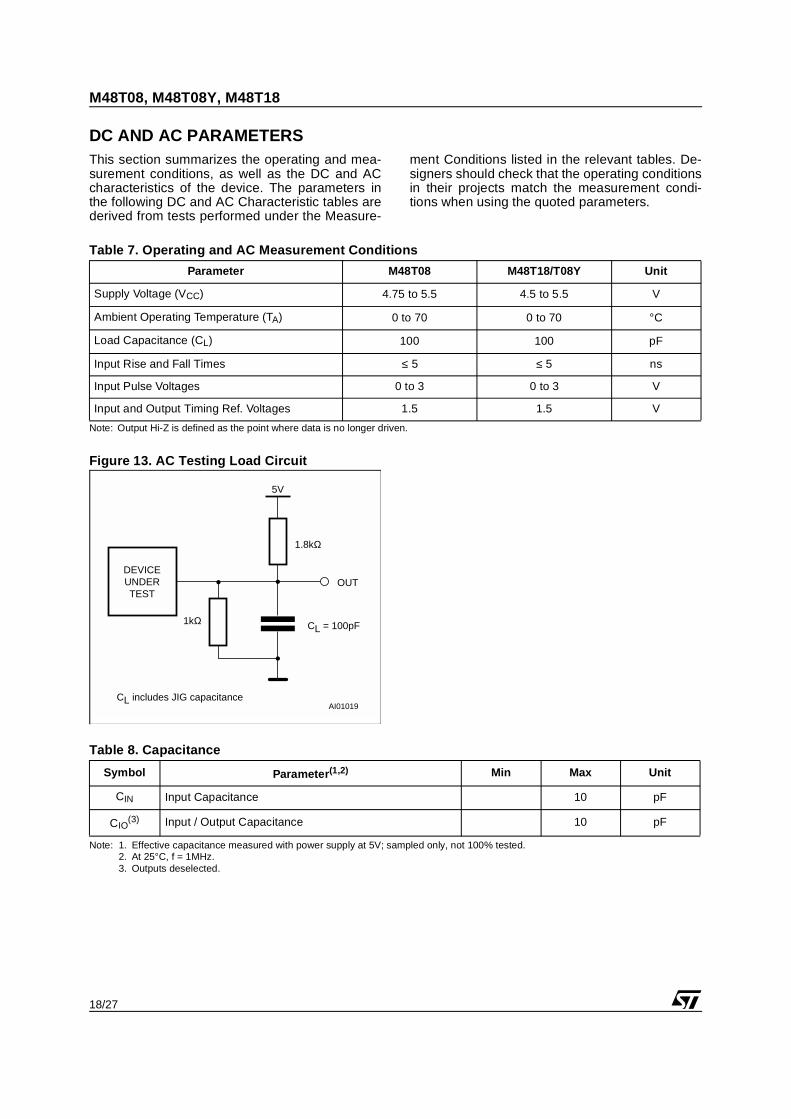
DC AND AC PARAMETERSThis section summarizes the operating and mea-surement conditions, as well as the DC and ACcharacteristics of the device. The parameters inthe following DC and AC Characteristic tables arederived from tests performed under the Measure-
ment Conditions listed in the relevant tables. De-signers should check that the operating conditionsin their projects match the measurement condi-tions when using the quoted parameters.
Table 7. Operating and AC Measurement Conditions
Note: Output Hi-Z is defined as the point where data is no longer driven.
Figure 13. AC Testing Load Circuit
Table 8. Capacitance
Note: 1. Effective capacitance measured with power supply at 5V; sampled only, not 100% tested.2. At 25°C, f = 1MHz.3. Outputs deselected.
Parameter M48T08 M48T18/T08Y Unit
Supply Voltage (VCC) 4.75 to 5.5 4.5 to 5.5 V
Ambient Operating Temperature (TA) 0 to 70 0 to 70 °C
Load Capacitance (CL) 100 100 pF
Input Rise and Fall Times ≤ 5 ≤ 5 ns
Input Pulse Voltages 0 to 3 0 to 3 V
Input and Output Timing Ref. Voltages 1.5 1.5 V
AI01019
5V
OUT
CL = 100pF
CL includes JIG capacitance
1.8kΩ
DEVICEUNDERTEST
1kΩ
Symbol Parameter(1,2) Min Max Unit
CIN Input Capacitance 10 pF
CIO(3) Input / Output Capacitance 10 pF
19/27
M48T08, M48T08Y, M48T18
Table 9. DC Characteristics
Note: 1. Valid for Ambient Operating Temperature: TA = 0 to 70°C; VCC = 4.75 to 5.5V or 4.5 to 5.5V (except where noted).2. Outputs deselected.3. Measured with Control Bits set as follows: R = '1'; W, ST, FT = '0.'4. The INT pin is Open Drain.
Symbol Parameter Test Condition(1)M48T08/M48T18/T08Y
UnitMin Max
ILI Input Leakage Current 0V ≤ VIN ≤ VCC ±1 µA
ILO(2) Output Leakage Current 0V ≤ VOUT ≤ VCC ±1 µA
ICC Supply Current Outputs open 80 mA
ICC1(3) Supply Current (Standby) TTL E1 = VIH, E2 = VIL 3 mA
ICC2(3) Supply Current (Standby) CMOS
E1 = VCC – 0.2V,E2 = VSS + 0.2V
3 mA
VIL Input Low Voltage –0.3 0.8 V
VIH Input High Voltage 2.2 VCC + 0.3 V
VOL
Output Low Voltage IOL = 2.1mA 0.4 V
Output Low Voltage (INT)(4) IOL = 0.5mA 0.4 V
VOH Output High Voltage IOH = –1mA 2.4 V
M48T08, M48T08Y, M48T18
20/27
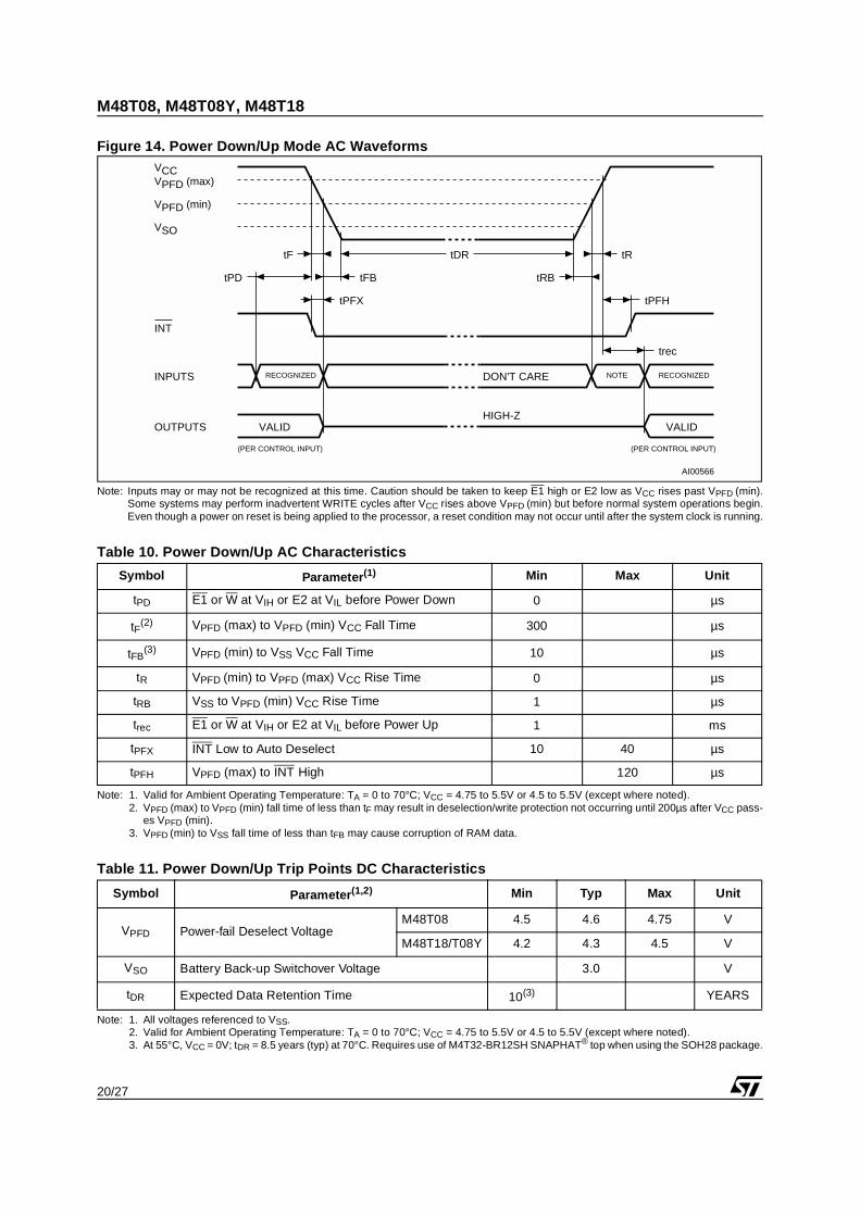
Figure 14. Power Down/Up Mode AC Waveforms
Note: Inputs may or may not be recognized at this time. Caution should be taken to keep E1 high or E2 low as VCC rises past VPFD (min).Some systems may perform inadvertent WRITE cycles after VCC rises above VPFD (min) but before normal system operations begin.Even though a power on reset is being applied to the processor, a reset condition may not occur until after the system clock is running.
Table 10. Power Down/Up AC Characteristics
Note: 1. Valid for Ambient Operating Temperature: TA = 0 to 70°C; VCC = 4.75 to 5.5V or 4.5 to 5.5V (except where noted).2. VPFD (max) to VPFD (min) fall time of less than tF may result in deselection/write protection not occurring until 200µs after VCC pass-
es VPFD (min).3. VPFD (min) to VSS fall time of less than tFB may cause corruption of RAM data.
Table 11. Power Down/Up Trip Points DC Characteristics
Note: 1. All voltages referenced to VSS.2. Valid for Ambient Operating Temperature: TA = 0 to 70°C; VCC = 4.75 to 5.5V or 4.5 to 5.5V (except where noted).3. At 55°C, VCC = 0V; tDR = 8.5 years (typ) at 70°C. Requires use of M4T32-BR12SH SNAPHAT® top when using the SOH28 package.
Symbol Parameter(1) Min Max Unit
tPD E1 or W at VIH or E2 at VIL before Power Down 0 µs
tF(2) VPFD (max) to VPFD (min) VCC Fall Time 300 µs
tFB(3) VPFD (min) to VSS VCC Fall Time 10 µs
tR VPFD (min) to VPFD (max) VCC Rise Time 0 µs
tRB VSS to VPFD (min) VCC Rise Time 1 µs
trec E1 or W at VIH or E2 at VIL before Power Up 1 ms
tPFX INT Low to Auto Deselect 10 40 µs
tPFH VPFD (max) to INT High 120 µs
Symbol Parameter(1,2) Min Typ Max Unit
VPFD Power-fail Deselect Voltage M48T08 4.5 4.6 4.75 V
M48T18/T08Y 4.2 4.3 4.5 V
VSO Battery Back-up Switchover Voltage 3.0 V
tDR Expected Data Retention Time 10(3) YEARS
AI00566
VCC
INPUTS
INT
(PER CONTROL INPUT)
OUTPUTS
DON'T CARE
HIGH-Z
tF
tFB
tPFX
tR
tPFH
trec
tPD tRB
tDR
VALID VALID
NOTE
(PER CONTROL INPUT)
RECOGNIZEDRECOGNIZED
VPFD (max)
VPFD (min)
VSO
21/27
M48T08, M48T08Y, M48T18
PACKAGE MECHANICAL INFORMATION
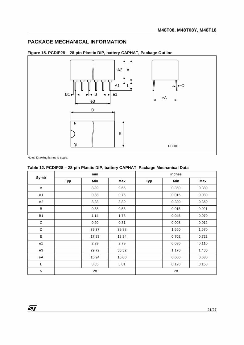
Figure 15. PCDIP28 – 28-pin Plastic DIP, battery CAPHAT, Package Outline
Note: Drawing is not to scale.
Table 12. PCDIP28 – 28-pin Plastic DIP, battery CAPHAT, Package Mechanical Data
Symbmm inches
Typ Min Max Typ Min Max
A 8.89 9.65 0.350 0.380
A1 0.38 0.76 0.015 0.030
A2 8.38 8.89 0.330 0.350
B 0.38 0.53 0.015 0.021
B1 1.14 1.78 0.045 0.070
C 0.20 0.31 0.008 0.012
D 39.37 39.88 1.550 1.570
E 17.83 18.34 0.702 0.722
e1 2.29 2.79 0.090 0.110
e3 29.72 36.32 1.170 1.430
eA 15.24 16.00 0.600 0.630
L 3.05 3.81 0.120 0.150
N 28 28
PCDIP
A2
A1
A
L
B1 B e1
D
E
N
1
C
eAe3
M48T08, M48T08Y, M48T18
22/27
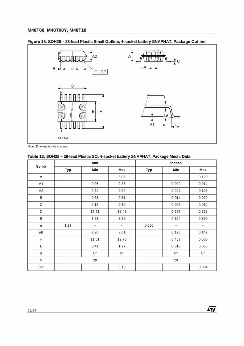
Figure 16. SOH28 – 28-lead Plastic Small Outline, 4-socket battery SNAPHAT, Package Outline
Note: Drawing is not to scale.
Table 13. SOH28 – 28-lead Plastic SO, 4-socket battery SNAPHAT, Package Mech. Data
Symbmm inches
Typ Min Max Typ Min Max
A 3.05 0.120
A1 0.05 0.36 0.002 0.014
A2 2.34 2.69 0.092 0.106
B 0.36 0.51 0.014 0.020
C 0.15 0.32 0.006 0.012
D 17.71 18.49 0.697 0.728
E 8.23 8.89 0.324 0.350
e 1.27 – – 0.050 – –
eB 3.20 3.61 0.126 0.142
H 11.51 12.70 0.453 0.500
L 0.41 1.27 0.016 0.050
α 0° 8° 0° 8°
N 28 28
CP 0.10 0.004
SOH-A
E
N
D
C
LA1 α1
H
A
CPB e
A2
eB
23/27
M48T08, M48T08Y, M48T18
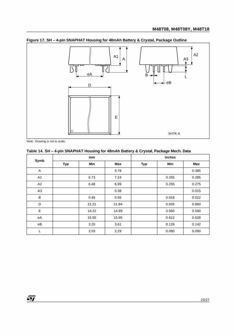
Figure 17. SH – 4-pin SNAPHAT Housing for 48mAh Battery & Crystal, Package Outline
Note: Drawing is not to scale.
Table 14. SH – 4-pin SNAPHAT Housing for 48mAh Battery & Crystal, Package Mech. Data
Symbmm inches
Typ Min Max Typ Min Max
A 9.78 0.385
A1 6.73 7.24 0.265 0.285
A2 6.48 6.99 0.255 0.275
A3 0.38 0.015
B 0.46 0.56 0.018 0.022
D 21.21 21.84 0.835 0.860
E 14.22 14.99 0.560 0.590
eA 15.55 15.95 0.612 0.628
eB 3.20 3.61 0.126 0.142
L 2.03 2.29 0.080 0.090
SHTK-A
A1A
D
E
eA
eB
A2
B L
A3
M48T08, M48T08Y, M48T18
24/27
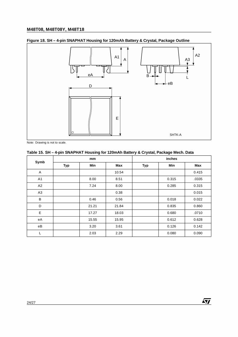
Figure 18. SH – 4-pin SNAPHAT Housing for 120mAh Battery & Crystal, Package Outline
Note: Drawing is not to scale.
Table 15. SH – 4-pin SNAPHAT Housing for 120mAh Battery & Crystal, Package Mech. Data
Symbmm inches
Typ Min Max Typ Min Max
A 10.54 0.415
A1 8.00 8.51 0.315 .0335
A2 7.24 8.00 0.285 0.315
A3 0.38 0.015
B 0.46 0.56 0.018 0.022
D 21.21 21.84 0.835 0.860
E 17.27 18.03 0.680 .0710
eA 15.55 15.95 0.612 0.628
eB 3.20 3.61 0.126 0.142
L 2.03 2.29 0.080 0.090
SHTK-A
A1A
D
E
eA
eB
A2
B L
A3
25/27
M48T08, M48T08Y, M48T18
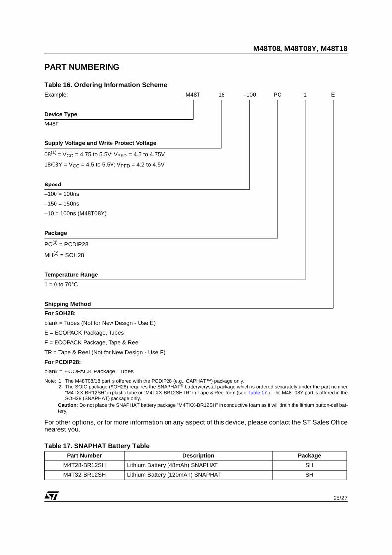
PART NUMBERING
Table 16. Ordering Information Scheme
Note: 1. The M48T08/18 part is offered with the PCDIP28 (e.g., CAPHAT™) package only.2. The SOIC package (SOH28) requires the SNAPHAT® battery/crystal package which is ordered separately under the part number
“M4TXX-BR12SH” in plastic tube or “M4TXX-BR12SHTR” in Tape & Reel form (see Table 17.). The M48T08Y part is offered in theSOH28 (SNAPHAT) package only.
Caution: Do not place the SNAPHAT battery package “M4TXX-BR12SH” in conductive foam as it will drain the lithium button-cell bat-tery.
For other options, or for more information on any aspect of this device, please contact the ST Sales Officenearest you.
Table 17. SNAPHAT Battery Table
Example: M48T 18 –100 PC 1 E
Device Type
M48T
Supply Voltage and Write Protect Voltage
08(1) = VCC = 4.75 to 5.5V; VPFD = 4.5 to 4.75V
18/08Y = VCC = 4.5 to 5.5V; VPFD = 4.2 to 4.5V
Speed
–100 = 100ns
–150 = 150ns
–10 = 100ns (M48T08Y)
Package
PC(1) = PCDIP28
MH(2) = SOH28
Temperature Range
1 = 0 to 70°C
Shipping Method
For SOH28:
blank = Tubes (Not for New Design - Use E)
E = ECOPACK Package, Tubes
F = ECOPACK Package, Tape & Reel
TR = Tape & Reel (Not for New Design - Use F)
For PCDIP28:
blank = ECOPACK Package, Tubes
Part Number Description Package
M4T28-BR12SH Lithium Battery (48mAh) SNAPHAT SH
M4T32-BR12SH Lithium Battery (120mAh) SNAPHAT SH
M48T08, M48T08Y, M48T18
26/27
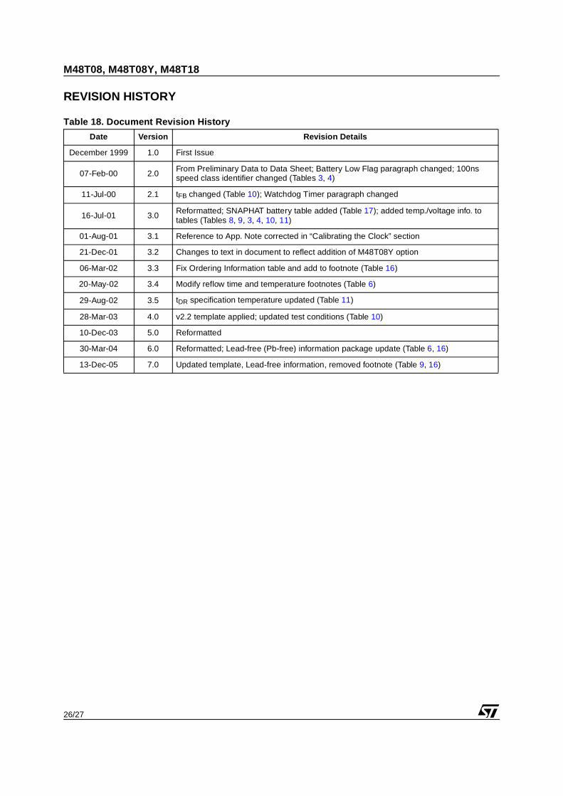
REVISION HISTORY
Table 18. Document Revision History
Date Version Revision Details
December 1999 1.0 First Issue
07-Feb-00 2.0From Preliminary Data to Data Sheet; Battery Low Flag paragraph changed; 100ns speed class identifier changed (Tables 3, 4)
11-Jul-00 2.1 tFB changed (Table 10); Watchdog Timer paragraph changed
16-Jul-01 3.0Reformatted; SNAPHAT battery table added (Table 17); added temp./voltage info. to tables (Tables 8, 9, 3, 4, 10, 11)
01-Aug-01 3.1 Reference to App. Note corrected in “Calibrating the Clock” section
21-Dec-01 3.2 Changes to text in document to reflect addition of M48T08Y option
06-Mar-02 3.3 Fix Ordering Information table and add to footnote (Table 16)
20-May-02 3.4 Modify reflow time and temperature footnotes (Table 6)
29-Aug-02 3.5 tDR specification temperature updated (Table 11)
28-Mar-03 4.0 v2.2 template applied; updated test conditions (Table 10)
10-Dec-03 5.0 Reformatted
30-Mar-04 6.0 Reformatted; Lead-free (Pb-free) information package update (Table 6, 16)
13-Dec-05 7.0 Updated template, Lead-free information, removed footnote (Table 9, 16)
27/27
M48T08, M48T08Y, M48T18
Information furnished is believed to be accurate and reliable. However, STMicroelectronics assumes no responsibility for the consequences of use of such information nor for any infringement of patents or other rights of third parties which may result from its use. No license is granted by implication or otherwise under any patent or patent rights of STMicroelectronics. Specifications mentioned in this publication are subject to change without notice. This publication supersedes and replaces all information previously supplied. STMicroelectronics products are not
authorized for use as critical components in life support devices or systems without express written approval of STMicroelectronics.
The ST logo is a registered trademark of STMicroelectronics.
All other names are the property of their respective owners
© 2005 STMicroelectronics - All rights reserved
STMicroelectronics group of companiesAustralia - Belgium - Brazil - Canada - China - Czech Republic - Finland - France - Germany - Hong Kong - India - Israel - Italy - Japan -
Malaysia - Malta - Morocco - Singapore - Spain - Sweden - Switzerland - United Kingdom - United States of Americawww.st.com