Embed Size (px)
Citation preview

The content and copyrights of the attached material are the property of its owner.
Distributed by:
www.Jameco.com 1-800-831-4242
1
2
3
4
5
6
7
8
VS GND
11
12
13
14
15
16
17
18
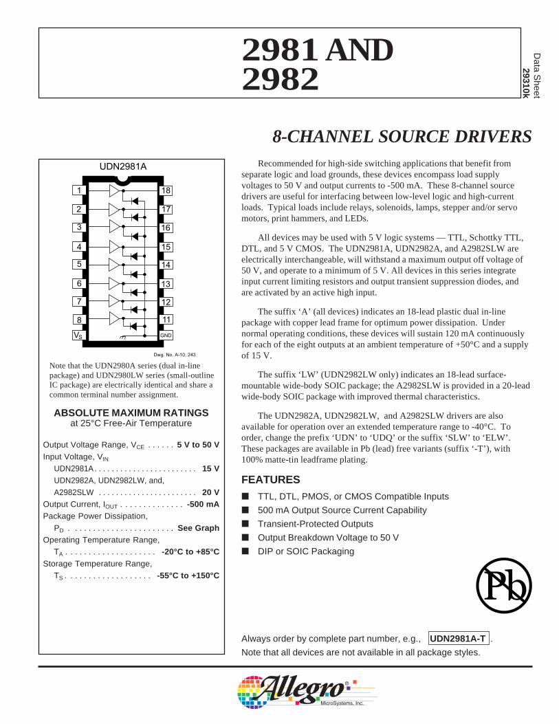
UDN2981A
Dwg. No. A-10, 243
Recommended for high-side switching applications that benefit fromseparate logic and load grounds, these devices encompass load supplyvoltages to 50 V and output currents to -500 mA. These 8-channel sourcedrivers are useful for interfacing between low-level logic and high-currentloads. Typical loads include relays, solenoids, lamps, stepper and/or servomotors, print hammers, and LEDs.
All devices may be used with 5 V logic systems — TTL, Schottky TTL,DTL, and 5 V CMOS. The UDN2981A, UDN2982A, and A2982SLW areelectrically interchangeable, will withstand a maximum output off voltage of50 V, and operate to a minimum of 5 V. All devices in this series integrateinput current limiting resistors and output transient suppression diodes, andare activated by an active high input.
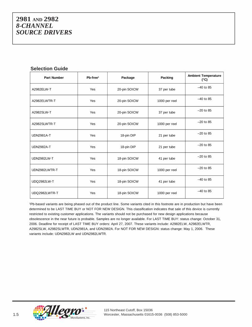
The suffix ‘A’ (all devices) indicates an 18-lead plastic dual in-linepackage with copper lead frame for optimum power dissipation. Undernormal operating conditions, these devices will sustain 120 mA continuouslyfor each of the eight outputs at an ambient temperature of +50°C and a supplyof 15 V.
The suffix ‘LW’ (UDN2982LW only) indicates an 18-lead surface-mountable wide-body SOIC package; the A2982SLW is provided in a 20-leadwide-body SOIC package with improved thermal characteristics.
The UDN2982A, UDN2982LW, and A2982SLW drivers are alsoavailable for operation over an extended temperature range to -40°C. Toorder, change the prefix ‘UDN’ to ‘UDQ’ or the suffix ‘SLW’ to ‘ELW’.These packages are available in Pb (lead) free variants (suffix ‘-T’), with100% matte-tin leadframe plating.
FEATURES TTL, DTL, PMOS, or CMOS Compatible Inputs
500 mA Output Source Current Capability
Transient-Protected Outputs
Output Breakdown Voltage to 50 V
DIP or SOIC Packaging
8-CHANNEL SOURCE DRIVERS
Always order by complete part number, e.g., UDN2981A-T .
Note that all devices are not available in all package styles.
ABSOLUTE MAXIMUM RATINGSat 25°C Free-Air Temperature
Output Voltage Range, VCE . . . . . . 5 V to 50 VInput Voltage, VIN
UDN2981A. . . . . . . . . . . . . . . . . . . . . . . . 15 VUDN2982A, UDN2982LW, and,
A2982SLW . . . . . . . . . . . . . . . . . . . . . . . 20 VOutput Current, IOUT . . . . . . . . . . . . . . -500 mAPackage Power Dissipation,
PD . . . . . . . . . . . . . . . . . . . . . . . See GraphOperating Temperature Range,
TA . . . . . . . . . . . . . . . . . . . . -20°C to +85°CStorage Temperature Range,
TS . . . . . . . . . . . . . . . . . . . -55°C to +150°C
Data S
heet29310k
2981 AND2982
Note that the UDN2980A series (dual in-linepackage) and UDN2980LW series (small-outlineIC package) are electrically identical and share acommon terminal number assignment.
2981 AND 29828-CHANNELSOURCE DRIVERS
115 Northeast Cutoff, Box 15036Worcester, Massachusetts 01615-0036 (508) 853-50002
1Pb-based variants are being phased out of the product line. Some variants cited in this footnote are in production but have been
determined to be LAST TIME BUY or NOT FOR NEW DESIGN. This classification indicates that sale of this device is currently
restricted to existing customer applications. The variants should not be purchased for new design applications because
obsolescence in the near future is probable. Samples are no longer available. For LAST TIME BUY: status change: October 31,
2006. Deadline for receipt of LAST TIME BUY orders: April 27, 2007. These variants include: A2982ELW, A2982ELWTR,
A2982SLW, A2982SLWTR, UDN2981A, and UDN2982A. For NOT FOR NEW DESIGN: status change: May 1, 2006. These
variants include: UDN2982LW and UDN2982LWTR.
Selection Guide
Part Number Pb-free1 Package PackingAmbient Temperature
(°C)
A2982ELW-T Yes 20-pin SOICW 37 per tube–40 to 85
A2982ELWTR-T Yes 20-pin SOICW 1000 per reel–40 to 85
A2982SLW-T Yes 20-pin SOICW 37 per tube–20 to 85
A2982SLWTR-T Yes 20-pin SOICW 1000 per reel–20 to 85
UDN2981A-T Yes 18-pin DIP 21 per tube–20 to 85
UDN2982A-T Yes 18-pin DIP 21 per tube–20 to 85
UDN2982LW-T Yes 18-pin SOICW 41 per tube–20 to 85
UDN2982LWTR-T Yes 18-pin SOICW 1000 per reel–20 to 85
UDQ2982LW-T Yes 18-pin SOICW 41 per tube–40 to 85
UDQ2982LWTR-T Yes 18-pin SOICW 1000 per reel–40 to 85
1.5
2981 AND 29828-CHANNELSOURCE DRIVERS
115 Northeas t C utoff, B ox 15036W orces ter, Mas s achus etts 01615-0036 (508) 853-50002
A2982SLW
50 75 100 125 150
2.5
0.5
0
AL
LO
WA
BL
EP
AC
KA
GE
PO
WE
RD
I SS
IPA
TIO
NIN
WA
TT
S
A MB IE NT T E MP E R A T UR E IN °°C
2.0
1.5
1.0
25
Dwg. G P -022-4A
18-LE AD S OIC , R J A = 94°C /W
20-LE AD S OIC , R J A = 90°C /W
18-P IN DIP , R θJ A = 65°C /W
One of Eight Drivers
OUT P UT
7.2 K
3 K
20 K
V 5
1.5 K
INP UT
G R OUND
9
Dwg. No. A-10,242USA
13
14
15
16
17
19
12
18
20
11NOC ONNE C T ION
1
2
3
8
9
4
5
6
7
10NOC ONNE C T ION
NCNC
Dwg. P P -064-2
G R OUND+VS
2981 AND 29828-CHANNEL
SOURCE DRIVERS
www.allegromicro.com 3
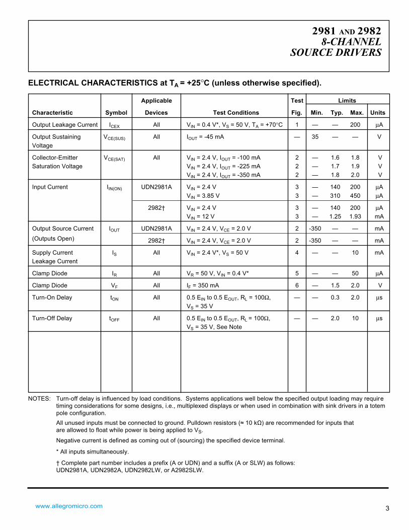
stimiLtseTelbacilppA
Characteristic Symbol Devices Test Conditions Fig. Min. Typ. Max. Units
Output Leakage Current ICEX All VIN = 0.4 V*, VS = 50 V, TA = +70°C 1 — — 200 µA
Output Sustaining VCE(SUS) All IOUT V——53—Am 54- = Voltage
Collector-Emitter VCE(SAT) All VIN = 2.4 V, IOUT = -100 mA 2 — 1.6 1.8 VVegatloV noitarutaS IN = 2.4 V, IOUT = -225 mA 2 — 1.7 1.9 VVIN = 2.4 V, IOUT = -350 mA 2 — 1.8 2.0 V
Input Current IIN(ON) UDN2981A VIN 002041—3V 4.2 = µAVIN 054013—3V 58.3 = µA
2982† VIN 002041—3V 4.2 = µAVIN Am39.152.1—3V 21 =
Output Source Current lOUT UDN2981A VIN = 2.4 V, VCE = 2.0 V 2 -350 — — mA
(Outputs Open) 2982† VIN = 2.4 V, VCE = 2.0 V 2 -350 — — mA
Supply Current IS All VIN = 2.4 V*, VS = 50 V 4 — — 10 mALeakage Current
Clamp Diode IR All VR = 50 V, VIN = 0.4 V* 5 — — 50 µA
Clamp Diode VF All IF V 0.25.1—6Am 053 =
Turn-On Delay tON All 0.5 EIN to 0.5 EOUT, RL = 100Ω, — — 0.3 2.0 µsVS = 35 V
Turn-Off Delay tOFF All 0.5 EIN to 0.5 EOUT, RL = 100Ω, — — 2.0 10 µsVS = 35 V, See Note
ELECTRICAL CHARACTERISTICS at TA = +25°C (unless otherwise specified).
NOTES: Turn-off delay is influenced by load conditions. Systems applications well below the specified output loading may requiretiming considerations for some designs, i.e., multiplexed displays or when used in combination with sink drivers in a totempole configuration.
Negative current is defined as coming out of (sourcing) the specified device terminal.
* All inputs simultaneously.
All unused inputs must be connected to ground. Pulldown resistors (≈ 10 kΩ) are recommended for inputs thatare allowed to float while power is being applied to VS.
† Complete part number includes a prefix (A or UDN) and a suffix (A or SLW) as follows:UDN2981A, UDN2982A, UDN2982LW, or A2982SLW.

2981 AND 29828-CHANNELSOURCE DRIVERS
115 Northeast Cutoff, Box 15036Worcester, Massachusetts 01615-0036 (508) 853-50004
TEST FIGURES
Figure 1 Figure 2 Figure 3
Dwg. No. A-11,083 Dwg. No. A-11,084 Dwg. No. A-11,085
V
VIN
CEXI
S
µAV
V
V
IOUT
IN
CE
S
VmA OPEN
V
VIN
INI
S
mA
Dwg. No. A-11,086 Dwg. No. A-11,087 Dwg. No. A-11,088
Figure 5 Figure 6Figure 4
OPEN
OPEN
V IFF V
VS
IR
VIN
µA
VIN
IS
SV
OPEN
mA
2981 AND 29828-CHANNEL
SOURCE DRIVERS
www.allegromicro.com 5
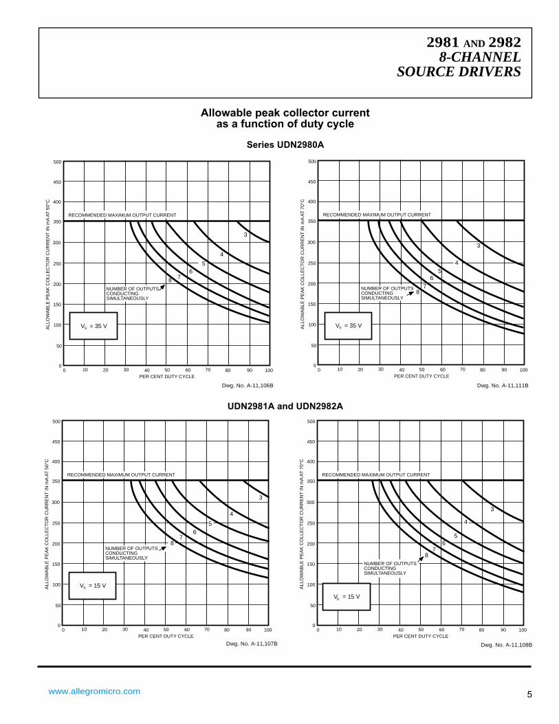
Allowable peak collector currentas a function of duty cycle
Series UDN2980A
100
V = 35 V
8 76
4
5
NUMBER OF OUTPUTSCONDUCTINGSIMULTANEOUSLY
90807060504030201000
50
100
150
200
250
300
350
400
450
500
RECOMMENDED MAXIMUM OUTPUT CURRENT
ALL
OW
AB
LE P
EA
K C
OLL
EC
TO
R C
UR
RE
NT
IN m
A A
T 5
0°C
PER CENT DUTY CYCLE
S
3
100
V = 35 V
87
6
45
NUMBER OF OUTPUTSCONDUCTINGSIMULTANEOUSLY
90807060504030201000
50
100
150
200
250
300
350
400
450
500
RECOMMENDED MAXIMUM OUTPUT CURRENT
ALL
OW
AB
LE P
EA
K C
OLL
EC
TO
R C
UR
RE
NT
IN m
A A
T 7
0°C
PER CENT DUTY CYCLE
S
3
Dwg. No. A-11,111BDwg. No. A-11,106B
UDN2981A and UDN2982A
100
V = 15 V
87
6
4
5
NUMBER OF OUTPUTSCONDUCTINGSIMULTANEOUSLY
90807060504030201000
50
100
150
200
250
300
350
400
450
500
RECOMMENDED MAXIMUM OUTPUT CURRENT
ALL
OW
AB
LE P
EA
K C
OLL
EC
TO
R C
UR
RE
NT
IN m
A A
T 5
0°C
PER CENT DUTY CYCLE
S
3
100
V = 15 V
87
6
4
5
NUMBER OF OUTPUTSCONDUCTINGSIMULTANEOUSLY
90807060504030201000
50
100
150
200
250
300
350
400
450
500
RECOMMENDED MAXIMUM OUTPUT CURRENT
ALL
OW
AB
LE P
EA
K C
OLL
EC
TO
R C
UR
RE
NT
IN m
A A
T 7
0°C
PER CENT DUTY CYCLE
S
3
Dwg. No. A-11,107B Dwg. No. A-11,108B
2981 AND 29828-CHANNELSOURCE DRIVERS
115 Northeast Cutoff, Box 15036Worcester, Massachusetts 01615-0036 (508) 853-50006
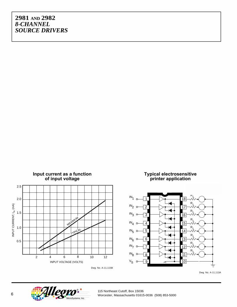
Input current as a functionof input voltage
Typical electrosensitiveprinter application
TYPICAL
2.5
INP
UT
CU
RR
EN
T, I
(m
A)
IN
2.0
1.5
1.0
0.5
2 4 6 8 10 12
INPUT VOLTAGE (VOLTS)
MAXIMUM
Dwg. No. A-11,115B
1
2
3
4
5
6
7
8
9
11
12
13
14
15
16
17
18
10
ELECTRODES
IN1
IN2
IN3
IN4
IN5
IN6
IN7
IN8
VS
RL
RL
RL
RL
RL
RL
RL
RL
Dwg. No. A-11,113A
2981 AND 29828-CHANNEL
SOURCE DRIVERS
www.allegromicro.com 7
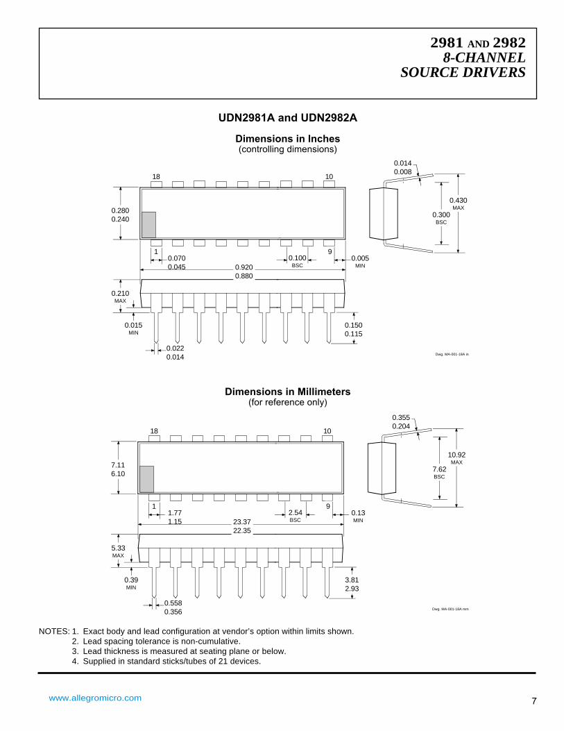
UDN2981A and UDN2982A
Dimensions in Inches(controlling dimensions)
Dimensions in Millimeters(for reference only)
0.0140.008
0.300BSC
Dwg. MA-001-18A in
0.430MAX
18
1 9
0.2800.240
0.210MAX
0.0700.045
0.015MIN
0.0220.014
0.100BSC
0.005MIN
0.1500.115
10
0.9200.880
NOTES: 1. Exact body and lead configuration at vendor’s option within limits shown.2. Lead spacing tolerance is non-cumulative.3. Lead thickness is measured at seating plane or below.4. Supplied in standard sticks/tubes of 21 devices.
0.3550.204
7.62BSC
Dwg. MA-001-18A mm
10.92MAX
18
1 9
7.116.10
5.33MAX
1.771.15
0.39MIN
0.5580.356
2.54BSC
0.13MIN
3.812.93
10
23.3722.35

2981 AND 29828-CHANNELSOURCE DRIVERS
115 Northeast Cutoff, Box 15036Worcester, Massachusetts 01615-0036 (508) 853-50008
UDN2982LW(add “TR” to part number for tape and reel)
Dimensions in Inches(for reference only)
Dimensions in Millimeters(controlling dimensions)
0° TO 8°1 2 30.020
0.013
0.0040 MIN.
0.01250.0091
0.0500.016
Dwg. MA-008-18A in
0.050BSC
18 10
0.4190.394
0.29920.2914
0.46250.4469
0.09260.1043
NOTES: 1. Exact body and lead configuration at vendor’s option within limits shown.2. Lead spacing tolerance is non-cumetive.3. Supplied in standard sticks/tubes of 41 devices or add “TR” to part number for tape and reel.
0° TO 8°1
18
2 30.510.33
0.10 MIN.
0.320.23
1.270.40
Dwg. MA-008-18A mm
1.27BSC
10
7.607.40
10.6510.00
11.7511.35
2.652.35
2981 AND 29828-CHANNEL
SOURCE DRIVERS
www.allegromicro.com 9
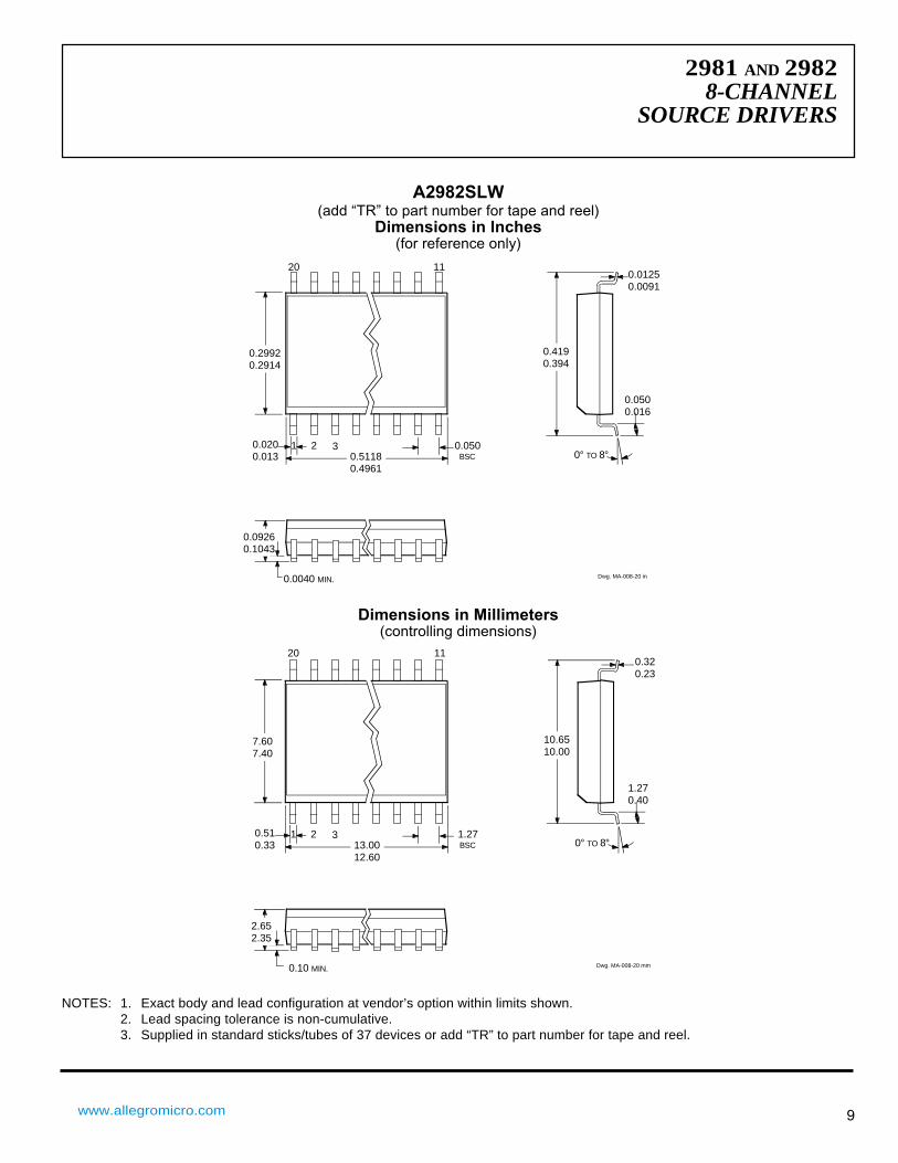
A2982SLW(add “TR” to part number for tape and reel)
Dimensions in Inches(for reference only)
Dimensions in Millimeters(controlling dimensions)
0° TO 8°1 2 30.020
0.013
0.0040 MIN.
0.01250.0091
0.0500.016
Dwg. MA-008-20 in
0.050BSC
20 11
0.29920.2914
0.4190.394
0.51180.4961
0.09260.1043
NOTES: 1. Exact body and lead configuration at vendor’s option within limits shown.2. Lead spacing tolerance is non-cumulative.3. Supplied in standard sticks/tubes of 37 devices or add “TR” to part number for tape and reel.
0° TO 8°1
20
2 30.510.33
0.10 MIN. Dwg. MA-008-20 mm
1.27BSC
110.320.23
1.270.40
7.607.40
10.6510.00
13.0012.60
2.652.35

2981 AND 29828-CHANNELSOURCE DRIVERS
115 Northeast Cutoff, Box 15036Worcester, Massachusetts 01615-0036 (508) 853-500010
Copyright ©1977, 2007, Allegro MicroSystems, Inc.
The products described here are manufactured under one or more U.S. patents or U.S. patents pending.
Allegro MicroSystems, Inc. reserves the right to make, from time to time, such departures from the detail specifications as may be required to
permit improvements in the performance, reliability, or manufacturability of its products. Before placing an order, the user is cautioned to verify
that the information being relied upon is current.
Allegro’s products are not to be used in life support devices or systems, if a failure of an Allegro product can reasonably be expected to cause the
failure of that life support device or system, or to affect the safety or effectiveness of that device or system.
The information included herein is believed to be accurate and reliable. However, Allegro MicroSystems, Inc. assumes no responsibility for its
use; nor for any infringement of patents or other rights of third parties which may result from its use.
For the latest version of this document, visit our website:www.allegromicro.com