Embed Size (px)
Citation preview
Distributed Power Conversion - An answer toPower Delivery Challenges in SoCs?
Rinkle Jain, Jim Tschanz, Vivek De
October 8 2014
Circuit Research Lab, Intel Corporation
Hillsboro, OR
Power Supply on Chip Workshop 2014
Acknowledgements
Vaibhav Vaidya
Stephen Kim
Seth Sanders
Krishnan Ravichandran
Chai Sutantavibul
Trang Ngyuen
Chung-ching Peng
Tri Huynh
Ken Ikeda
Carlos Tokunaga
Muhammad Khellah
Rick Forand
This research was, in part, funded by the U.S. Government (DARPA). The views and conclusions
contained in this document are those of the authors and should not be interpreted as representing
the official policies, either expressed or implied, of the U.S. Government.
2/ 24
Outline
Motivation for fully integrated VRs
Capability of Switched Capacitor Voltage Regulator (SCVR)
DVFS enabler with minimum area-power overhead
Co-design with load
Summary and Conclusion
3/ 24
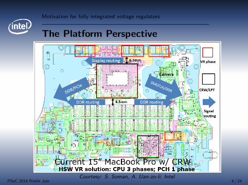
Motivation for fully integrated voltage regulators
The Platform Perspective
Courtesy: S. Soman, A. Uan-zo-li; IntelPSoC 2014 Rinkle Jain 4 / 24
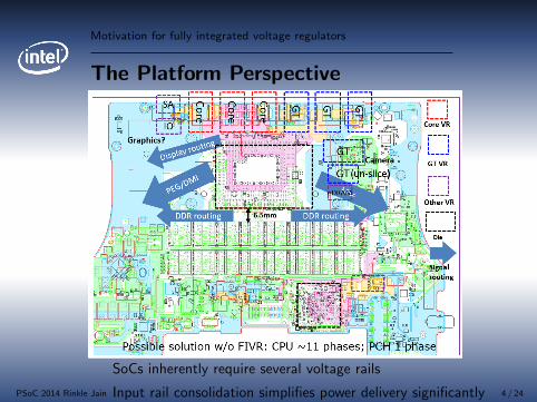
Motivation for fully integrated voltage regulators
The Platform Perspective
SoCs inherently require several voltage rails
Input rail consolidation simplifies power delivery significantlyPSoC 2014 Rinkle Jain 4 / 24
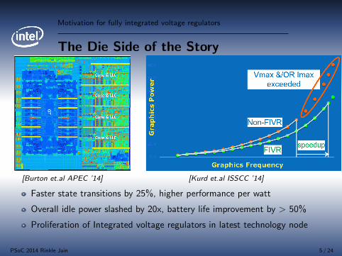
Motivation for fully integrated voltage regulators
The Die Side of the Story
[Burton et.al APEC ’14] [Kurd et.al ISSCC ’14]
Faster state transitions by 25%, higher performance per watt
Overall idle power slashed by 20x, battery life improvement by > 50%
Proliferation of Integrated voltage regulators in latest technology node
PSoC 2014 Rinkle Jain 5 / 24
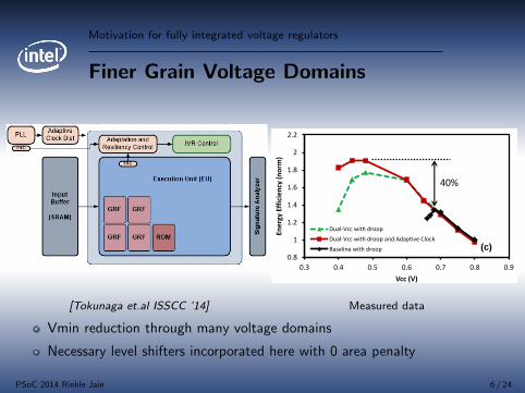
Motivation for fully integrated voltage regulators
Finer Grain Voltage Domains0
0.2
0.4
0.6
0.8
1
1.2
1.4
1.6
1.8
0 200 400 600 800 1000 1200
Po
wer
(n
orm
)
Frequency (MHz)
Dual-Vcc with droop
Dual-Vcc with droop and Adaptive Clock
Baseline with droop
0.8
1
1.2
1.4
1.6
1.8
2
2.2
0.3 0.4 0.5 0.6 0.7 0.8 0.9
Ene
rgy
Effi
cien
cy (
no
rm)
Vcc (V)
Dual-Vcc with droop
Dual-Vcc with droop and Adaptive Clock
Baseline with droop
Figure 6. (a) FMAX recovery for different Adaptive Clock Distribution lengths.
(b) Power vs. frequency for baseline design, baseline with adaptive clocking, and dual-VCC design with adaptive clocking.
(c) Energy efficiency vs. VCC.
(a)
(b)
(c)
0.0%
2.0%
4.0%
6.0%
8.0%
10.0%
12.0%
14.0%
1 2 3 4 5 6 7 8
FMax
De
grad
atio
n
ACD Delay in Clock Cycles
90% FMAX recovery
FMAX degradation without adaptive clocking
40%
0.67V
0.38V
27%
12.4%
0.8V
[Tokunaga et.al ISSCC ’14] Measured data
Vmin reduction through many voltage domains
Necessary level shifters incorporated here with 0 area penalty
PSoC 2014 Rinkle Jain 6 / 24
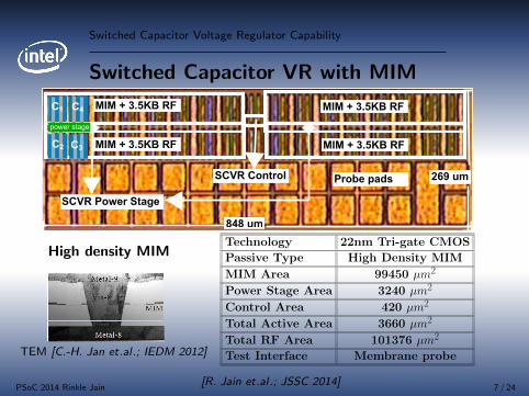
Switched Capacitor Voltage Regulator Capability
Switched Capacitor VR with MIM
MIM + 3.5KB RF
MIM + 3.5KB RF
MIM + 3.5KB RF
MIM + 3.5KB RF
SCVR Control
SCVR Power Stage
Probe pads
848 um
269 um
C1 C4
C3C2
power stage
High density MIM
TEM [C.-H. Jan et.al .; IEDM 2012]
Technology 22nm Tri-gate CMOS
Passive Type High Density MIM
MIM Area 99450 µm2
Power Stage Area 3240 µm2
Control Area 420 µm2
Total Active Area 3660 µm2
Total RF Area 101376 µm2
Test Interface Membrane probe
[R. Jain et.al .; JSSC 2014]PSoC 2014 Rinkle Jain 7 / 24
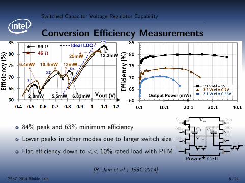
Switched Capacitor Voltage Regulator Capability
Conversion Efficiency Measurements
Vout (V)
99 Ω46 Ω 13.3mW
2.8mW 5.5mW 6.83mW
6.4mW 10.4mW 13mW25mW
2:1
3:25:4
1:1Ideal LDO
Output Power (mW)
84% peak and 63% minimum efficiency
Lower peaks in other modes due to larger switch size
Flat efficiency down to << 10% rated load with PFMS10
S11
S21
S31
Vin
Vout
C1 C2
Power Cell
S41
S51
S61
S71
S81S91
[R. Jain et.al .; JSSC 2014]
PSoC 2014 Rinkle Jain 8 / 24
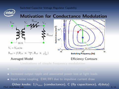
Switched Capacitor Voltage Regulator Capability
Motivation for Conductance ModulationVin Vo
m:n
++
--
Rout = f (Rfsl ∝ rdsond , Rssl ∝ 1
Cfsw)
Rload
Ve
Ve = Vinn/m
Rout
Averaged Model Efficiency Contours
Limitations of simple frequency modulation
Lower-than-optimal conversion efficiency at lower voltages
Increased output ripple and associated power loss at light loads
Input noise coupling. EMI/RFI due to impulsive current draw
Other knobs: 1/rdson (conductance), C (fly capacitance), d(duty)PSoC 2014 Rinkle Jain 9 / 24
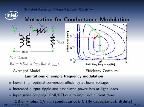
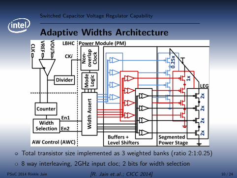
Switched Capacitor Voltage Regulator Capability
Adaptive Widths Architecture
Buffers + Level Shifters
SegmentedPower Stage
Wid
th A
sse
rt
0.2
5x
1x
2x
2x
2x
2x
En1
En2Width
Selection
VO
UT
VR
EF
CLK
Counter
Power Module (PM)
Divider
LBHC
AW Control (AWC)
LEGN
on
-o
ve
rla
pC
lockCKi
Mo
de
Lo
gic
Total transistor size implemented as 3 weighted banks (ratio 2:1:0.25)
8 way interleaving, 2GHz input cloc; 2 bits for width selection
[R. Jain et.al .; CICC 2014]PSoC 2014 Rinkle Jain 10 / 24
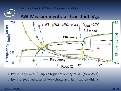
Switched Capacitor Voltage Regulator Capability
AW Measurements at Constant Vref
fsw < FthW = bW ′
a implies higher efficiency at W’ (W’=W/n)
fsw is a good indicator of low voltage and light load conditions
PSoC 2014 Rinkle Jain 11 / 24
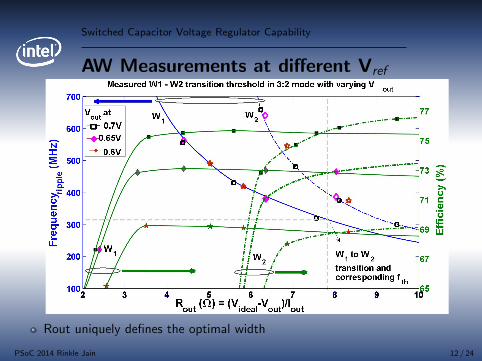
Switched Capacitor Voltage Regulator Capability
AW Measurements at different Vref
Rout uniquely defines the optimal width
PSoC 2014 Rinkle Jain 12 / 24
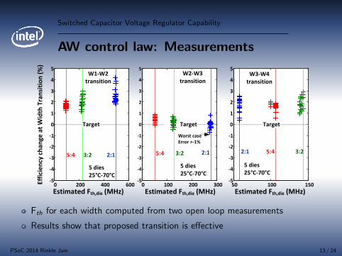
Switched Capacitor Voltage Regulator Capability
AW control law: Measurements
200 400 600 0 200 400 600 800-3
-2
-1
0
1
2
3
0 50 100 150 200-3
-2
-1
0
1
2
3
50 100 150-5
-4
-3
-2
-1
0
1
2
3
4
5
0 100 200 300-5
-4
-3
-2
-1
0
1
2
3
4
5
Target
0 200 400 600-5
-4
-3
-2
-1
0
1
2
3
4
5
3:25:42:1
Target
W3-W4
transition
5 dies
25°C-70°C
W2-W3
transition
3:25:4 2:1
5 dies
25°C-70°C
W1-W2
transition
2:13:25:4
Target
5 dies
25°C-70°C
Automatically switching to a smaller transistor size (or width, W1>W2>W3>W4) at lighter load, when
it becomes just as efficient as larger size (efficiency difference =0) :
Measured efficiency difference at automated transition frequency Fth, different dies/temperatures
Eff
icie
ncy
ch
an
ge
at
Wid
th T
ran
siti
on
(%
)
Worst case
Error >-1%
Estimated Fth,die (MHz) Estimated Fth,die (MHz)Estimated Fth,die (MHz)
Fth for each width computed from two open loop measurements
Results show that proposed transition is effective
PSoC 2014 Rinkle Jain 13 / 24
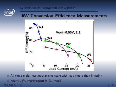
Switched Capacitor Voltage Regulator Capability
AW Conversion Efficiency Measurements
0 5 10 15 20 2570
75
80
85Vout=0.55V, 2:1
Effic
ienc
y(%
)
Load Current (mA)
W3
W4
W2
W1
All three major loss mechanisms scale with load (more than linearly)
Nearly 15% improvement in 2:1 modePSoC 2014 Rinkle Jain 14 / 24
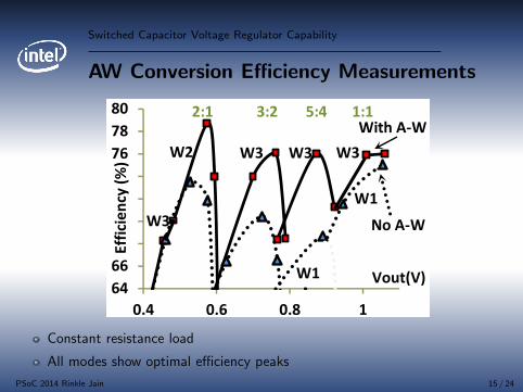
Switched Capacitor Voltage Regulator Capability
AW Conversion Efficiency Measurements
64
66
68
70
72
74
76
78
80
0.4 0.6 0.8 1
W3
W3
W3W3W2
W1
Vout(V)
Eff
icie
ncy
(%
)2:1 3:2 5:4 1:1
With A-W
No A-W
W1
Constant resistance load
All modes show optimal efficiency peaks
PSoC 2014 Rinkle Jain 15 / 24
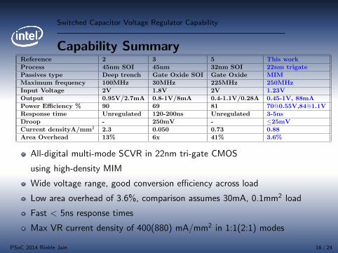
Switched Capacitor Voltage Regulator Capability
Capability SummaryReference 2 3 5 This workProcess 45nm SOI 45nm 32nm SOI 22nm trigatePassives type Deep trench Gate Oxide SOI Gate Oxide MIMMaximum frequency 100MHz 30MHz 225MHz 250MHzInput Voltage 2V 1.8V 2V 1.23VOutput 0.95V/2.7mA 0.8-1V/8mA 0.4-1.1V/0.28A 0.45-1V, 88mAPower Efficiency % 90 69 81 [email protected],[email protected] time Unregulated 120-200ns Unregulated 3-5nsDroop - 250mV - ≤25mVCurrent densityA/mm2 2.3 0.050 0.73 0.88Area Overhead 13% 6x 41% 3.6%
All-digital multi-mode SCVR in 22nm tri-gate CMOS
using high-density MIM
Wide voltage range, good conversion efficiency across load
Low area overhead of 3.6%, comparison assumes 30mA, 0.1mm2 load
Fast < 5ns response times
Max VR current density of 400(880) mA/mm2 in 1:1(2:1) modes
PSoC 2014 Rinkle Jain 16 / 24
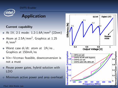
DVFS Enabler
Application
Current capability
At 1V, 2:1 mode: 1.2-1.6A/mm2 (22nm)
Atom at 2.5A/mm2, Graphics at 1.25A/mm2
Worst case di/dt: atom at 2A/ns ,Graphics at 150mA/ns
Vin=Vccmax feasible, downconversion isnot a must
Reuse power gates, hybrid solution withLDO
Minimum active power and area overhead
0.4 0.6 0.8 1Output Voltage [V]
1:1
5:43:2
2:1
3:1
Effic
ienc
y [%
]
Bypassmode
Digital LDOSCVR
100 200 300 400 500 600 7000
0.2
0.4
0.6
0.8
1
Frequency [MHz]Nor
mal
ized
Pow
er C
onsu
mpt
ion
DFS ext rail
0
0.2
0.4
0.6
0.8
1
Nor
mal
ized
Pow
er C
onsu
mpt
ion
DVFS SCVR with bypassDVFS ext railDVFS with IVR, 85% eff
PSoC 2014 Rinkle Jain 17 / 24
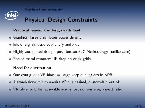
Distributed Implementation
Physical Design Constraints
Practical issues: Co-design with load
Graphics: large area, lower power density
lots of signals traverse x and y and x<y
Highly automated design, push button SoC Methodology (unlike core)
Shared metal resources, IR drop on weak grids
Need for distribution
One contiguous VR block ⇒ large keep-out-regions in APR
A stand-alone minimum-size VR tile desired, custom-laid out ok
VR tile should be reuse-able across loads of any size, aspect ratio
PSoC 2014 Rinkle Jain 18 / 24
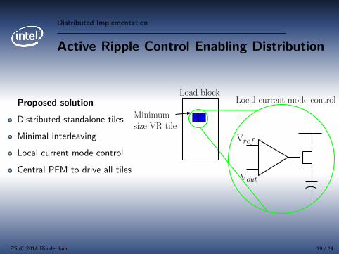
Distributed Implementation
Active Ripple Control Enabling Distribution
Proposed solution
Distributed standalone tiles
Minimal interleaving
Local current mode control
Central PFM to drive all tiles
Vref
Vout
Local current mode controlLoad block
Minimumsize VR tile
PSoC 2014 Rinkle Jain 19 / 24
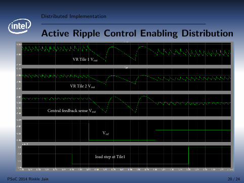
Distributed Implementation
Active Ripple Control Enabling Distribution
VR Tile 1 Vout
VR Tile 2 Vout
Central feedback sense Vout
Vref
load step at Tile1
PSoC 2014 Rinkle Jain 20 / 24
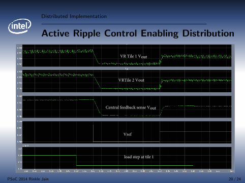
Distributed Implementation
Active Ripple Control Enabling Distribution
Vref
Central feedback sense
Tile 2 Vout
PSoC 2014 Rinkle Jain 20 / 24
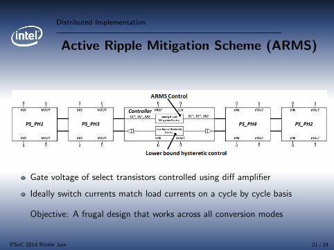
Distributed Implementation
Active Ripple Mitigation Scheme (ARMS)
Gate voltage of select transistors controlled using diff amplifier
Ideally switch currents match load currents on a cycle by cycle basis
Objective: A frugal design that works across all conversion modes
PSoC 2014 Rinkle Jain 21 / 24
Distributed Implementation
Active Ripple Mitigation Scheme (ARMS)
Powerstage Schematic
Adaptive Gate Driver (AD)
Low ‐Bound Hysteretic Control(LBHC )
ARMS in 2:1 Operation
VPVN
VB
AMP_OUT
MP
MN
S1
C1 C2 C3 C4VOUT
LEG
S2
S3
S4
LEG LEG LEG
VOUT
G42
G41
G81
G82
VOUT
VREF An
alo g
Mu x
Analo g
Swi tc
hAn a
logSw
i tch
G12
G11
G51
G52
ARMS Control (ARMC)
LEG
AD
AD
VOUT
VREF
CLK
D Q D Q D Q D Q
CK1 CK2 CK3 CK4
PSoC 2014 Rinkle Jain 21 / 24
Distributed Implementation
ARMS Ripple Measurements
0.020.040.060.080.10
0.45 0.55 0.65V_MIN (V)
V_PK
-PK
(V)
: ARMS ON CL: ARMS OFF: ARMS ON OL
2:1 3:2 5:4
50mV/Div. 100ns/Div.
ARMS OFF
ARMS Optimum Setting (OL)
ARM
S Sh
uttin
g Do
wn
0.70
0.75
0.80
0.850.90
0.20 0.30 0.40 0.50
PUF
V_MIN (V)
: ARMS OFF: ARMS ON OL
2:1 3:25:4
VOUT
VREF
CLK
ARMS Control
OLCL
PS_PH4
PS_PH3
PS_PH2
PS_PH1
LBHC
During OL, VREF can be tuned for optimum Condition for ARMS
0.020.040.060.080.10
0.45 0.55 0.65V_MIN (V)
V_PK
-PK
(V)
: ARMS ON CL: ARMS OFF: ARMS ON OL
50mV/Div. 100ns/Div.
ARMS OFF
ARMS Optimum Setting (OL)
ARM
S Sh
uttin
g Do
wn
0.70
0.75
0.80
0.850.90
0.20 0.30 0.40 0.50
PUF
V_MIN (V)
: ARMS OFF: ARMS ON OL
5:4
VOUT
VREF
CLK
ARMS Control
OLCL
PS_PH4
PS_PH3
PS_PH2
PS_PH1
LBHC
During OL, VREF can be tuned for optimum Condition for ARMS
3:22:1
2:1 3:2 5:40.2V
100
80
60
40
20
Vpkpk
(mV)
Vout (V)90
ARMS ON ARMS OFF
0.45 0.652:1 3:2 5:4
Load, Vout independent ripple
Minimum size VR tile
PSoC 2014 Rinkle Jain 22 / 24
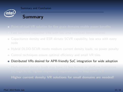
Summary and Conclusion
Summary
Point-of-load VR solution for fine grain domains enable power benefits
Fast switched capacitor VRs with low area overhead demonstrated
Capacitance density and ESR dictate SCVR capability, less area with everynode
Hybrid DLDO-SCVR meets medium current density loads, no power penalty
Control techniques ensure optimal efficiency and small VR tiles
Distributed VRs desired for APR-friendly SoC integration for wide adoption
High-current-density loads may have (i) few bumps or platform limitations.(ii) high di/dt, tighter impedance requirements ⇒ step down IVR
Higher current density VR solutions for small domains are needed!
PSoC 2014 Rinkle Jain 23 / 24

Thank you for your attention!
PSoC 2014 Rinkle Jain 24 / 24