Embed Size (px)
Citation preview

Distributed Power Conversion Architecture for
Microgrids and Integration of
Renewable Energy Sources
by
Junjian Zhao
A thesis submitted in partial fulfillment of
the requirement for the degree of
Master of Science
(Electrical and Computer Engineering)
at the
UNIVERSITY OF WISCONSIN-MADISON
2013

© Copyright by Junjian Zhao 2013
All Rights Reserved

Distributed Power Conversion Architecture for
Microgrids and Integration of
Renewable Energy Sources
by
Junjian Zhao
Under the supervision of Professor Yehui Han
at the University of Wisconsin – Madison
Approved by: ______________________
Yehui Han
Date: _____________________


I
ABSTRACT
This article focuses on distributed power conversion architecture for microgrid
and integration of renewable energy sources from the aspect of power electronics
converter.
It covers the following areas: Power Distribution and Control, Alternative Power
and Energy Technology, Energy Storage Technology, Energy Conversion and
Efficiencies.
The state-of-the-art research of microgrid, control algorithms and power
electronics building blocks are reviewed in this article. We propose a distributed power
conversion architecture for renewable energy sources in microgrids, which has
advantages including functionality, efficiency, reliability, and low manufacturing cost.
Its impact on future grids is investigated. The physical system in University of
Wisconsin-Milwaukee is studied. A family of DAB converter based power electronics
building block is proposed to realize the modular design consideration. The modeling
and control algorithms of the DC and AC power electronics building blocks are
developed and simulation results have verified the theoretical model.

II
This research also opens up new possibilities for how renewable energy sources
can be integrated and applied.
Keywords: Renewable Energy Power Conversion Microgrid
Power Electronics Building Blocks

III
ACKNOWLEDGMENTS
First and foremost, I would like to extend my deep appreciation towards my
advisor, Professor Yehui Han, for his generous support and guidance during the project.
His experience in the field of power electronics, and his willingness to share it with his
colleagues and students, remain as a great source of inspiration to me.
Secondly, I feel indebted to all other faculty members of Wisconsin Electric
Machinery and Power Electronics Consortium (WEMPEC). Their lectures furthered
my understanding of machines and power electronics and built the foundation of my
research.
I gratefully acknowledge Wisconsin Energy Research Consortium (WERC) for
the financial support of this project.
I would like to thank Prof. Yu’s group, especially Carl and Qiang from University
of Wisconsin-Milwaukee for their work from power system side and preparing the
final report of this project.
I appreciate the help of Liang Wang from Tsinghua University, he helped to
improve converter control algorithms.

IV
I would like to thank all my WEMPEC colleagues, especially Jiyao, Ye, Bo, Tim,
Kenton, Silong, Joyce, Di, Yingjie, Minjie, and Yukai for making my life in Madison
enjoyable and meaningful.
Finally, I would like to thank my parents and my girlfriend Emily X. Zhang for
their love and support all these years.

V
TABLE OF CONTENTS
ABSTRACT ……….…………………………………………………………..I
ACKNOWLEDGMENTS ..........................................................................III
TABLE OF CONTENTS ............................................................................ V
LIST OF FIGURES .................................................................................. IX
LIST OF TABLES ................................................................................. XIII
Chapter 1 Background ..........................................................................1
1.1 The picture of a Microgrid ...................................................................1
1.1.1 Distributed Generators ....................................................................2
1.1.2 Energy Storage Devices ..................................................................6
1.1.3 Distributed Power Conversion Architecture .....................................7
1.1.4 Microgrid Loads .............................................................................9
1.2 Technical Challenges for Power Conversion in Microgrids ...................9
1.3 Outline of the Thesis ......................................................................... 12
Chapter 2 State of the Art Review ...................................................... 15
2.1 System Level - Microgrid State of the Art .......................................... 15
2.1.1 AC Microgrid and Applications ..................................................... 15
2.1.2 DC Microgrid and Applications ..................................................... 21
2.1.3 Hybrid AC/DC Microgrid and Applications ................................... 24
2.2 Control Level - Droop Control in Microgrids State of the Art ............. 29
2.2.1 Droop Control in AC Microgrids ................................................... 31
2.2.2 Droop Control in DC Microgrids ................................................... 34
2.2.3 Droop Control in Hybrid AC/DC Microgrids ................................. 36
2.3 Converter Level - Power Electronics Building Block (PEBB) State of the
Art .......................................................................................................... 38
2.3.1 The Concept of PEBB ................................................................... 38
2.3.2 Plug and Play ................................................................................ 41

VI
2.3.3 Modeling and Hierarchical Control of PEBB ................................. 43
Chapter 3 PEBB Based Power Conversion Architecture for DC
Microgrids…….. ... ……………………………………………………………..49
3.1 Proposed Architecture ....................................................................... 49
3.2 Realization in UW-Milwaukee Microgrid ........................................... 53
3.3 DC Bus Voltage Level ....................................................................... 57
3.3.1 DC Bus Voltage Identification ...................................................... 57
3.3.2 The Advantages of 380V DC Bus Voltage ..................................... 59
3.4 PEBB Topology Selection – Bidirectional Dual Active Bridge ........... 62
3.4.1 The overview of PEBB Topology Candidates ................................ 62
3.4.2 Single-Stage Topologies ............................................................... 67
3.4.3 Two-Stage Topologies .................................................................. 73
3.4.4 PEBB Topology Identification ...................................................... 74
3.5 Modular Design Considerations ......................................................... 75
Chapter 4 Modeling of DAB Based PEBBs ......................................... 81
4.1 Modeling of DAB based DC/DC PEBBs ............................................ 82
4.1.1 Lossless Model of Single Phase DC/DC DAB ............................... 82
4.1.2 Average Model of Single Phase DC/DC DAB ................................ 83
4.1.3 Small Signal Model of Single Phase DC/DC DAB ......................... 84
4.1.4 Three Phase DAB based DC/DC PEBBs ........................................ 86
4.2 Modeling of DAB based AC/DC PEBBs ............................................ 86
4.2.1 Solution 1: Combination of Traditional AC/DC topology and DC/DC
DAB ...................................................................................................... 87
4.2.2 Solution 2: Pure Single Phase AC/DC DAB .................................. 89
Chapter 5 Control Algorithms and Simulation of PEBBs ..................... 91
5.1 Control Method for Single Phase DC/DC DAB .................................. 91
5.1.1 Phase Shift Modulation ................................................................. 91
5.1.2 Closed-loop Control ...................................................................... 93
5.2 Control Method for Traditional Three Phase AC/DC Converter .......... 94
5.3 Control Method for Single Phase AC/DC DAB .................................. 98
5.4 Control Method for Three Phase AC/DC DAB ................................. 100

VII
5.5 Simulation Results........................................................................... 102
5.5.1 Simulation of DC/DC Single Phase DAB .................................... 102
5.5.2 Simulation of AC/DC Single Phase DAB .................................... 109
5.5.3 Simulation of Traditional Three Phase AC/DC Converter ............ 113
5.5.4 Simulation of Three Phase AC/DC DAB ..................................... 124
Chapter 6 Conclusion and Future Work ............................................ 131
References………………. ......................................................................... 133

VIII

IX
LIST OF FIGURES
Figure 1.1 Centralized utility vs. distributed generator-based utility ......3
Figure 1.2 Global greenhouse gas (GHG) abatement cost curve 2030 [3]4
Figure 1.3 Centralized power conversion architecture .......................... 10
Figure 2.1 CERTS Microgrid Architecture ........................................... 16
Figure 2.2 Real power droop curve for power sharing .......................... 19
Figure 2.3 University of Wisconsin-Madison Microgrid Architecture ... 21
Figure 2.4 EPRI 380V-DC data center distribution [14] ....................... 23
Figure 2.5 (a) Typical AC distribution vs. (b) Standard 380V DC
distribution [14] ......................................................................................... 25
Figure 2.6 An example of hybrid AC/DC microgrid ............................. 27
Figure 2.7 Typical hybrid AC/DC microgrid structure ......................... 29
Figure 2.8 Active and reactive power droop characteristic for AC
microgrid……………… .............................................................................. 33
Figure 2.9 Active power droop characteristic for DC microgrid ........... 36
Figure 2.10 Power Electronics Building Block....................................... 39
Figure 2.11 PEBB concept for power electronics ................................... 46
Figure 3.1 Proposed distributed power conversion architecture ............ 50
Figure 3.2 University of Wisconsin-Milwaukee microgrid map ............ 53
Figure 3.3 DC bus voltage selection overview ..................................... 57
Figure 3.4 Comparison of energy usage for different system voltages .. 58
Figure 3.5 Comparison of conductor diameters (courtesy of UECorp)
[14]…………… .......................................................................................... 62
Figure 3.6 General structure of an isolated, bidirectional DC/DC
converter………………….. ......................................................................... 64
Figure 3.7 Family tree of single-stage and two-stage bidirectional isolated
DC/DC topologies ...................................................................................... 66
Figure 3.8 Single phase DAB converter ............................................... 68
Figure 3.9 Three phase DAB converter ................................................ 69
Figure 3.10 Voltage sourced full bridge with a current sourced full bridge

X
converter………….. .................................................................................... 70
Figure 3.11 Voltage sourced full bridge with a current doubler .............. 71
Figure 3.12 Voltage sourced full bridge with a push-pull structure on low
voltage side……. ........................................................................................ 71
Figure 3.13 Bidirectional series-parallel resonant LLC converter ........... 72
Figure 3.14 Bidirectional series-parallel resonant LCC converter ........... 72
Figure 3.15 Two stage converter with buck converter on high voltage
side……………………… ............................................................................ 74
Figure 3.16 DC/DC PEBB modular ....................................................... 76
Figure 3.17 AC/DC PEBB modular ....................................................... 76
Figure 3.18 AC/AC PEBB modular ....................................................... 77
Figure 4.1 Single phase DC/DC DAB .................................................. 82
Figure 4.2 Single phase DC/DC DAB lossless model ........................... 83
Figure 4.3 Traditional three phase AC/DC converter ............................ 87
Figure 4.4 Single phase AC/DC DAB .................................................. 89
Figure 4.5 Single phase AC/DC DAB based three phase AC/DC PEBB 90
Figure 5.1 Control schematic of single phase DC/DC DAB .................. 93
Figure 5.2 Control block diagram of single phase DC/DC DAB ........... 94
Figure 5.3 Block diagram of dq frame decouple control for traditional
three phase AC/DC converter ...................................................................... 96
Figure 5.4 Control block diagram of traditional AC/DC converter ........ 97
Figure 5.5 Control algorithm of single phase AC/DC DAB ................ 100
Figure 5.6 Block diagram of single phase AC/DC DAB with controller100
Figure 5.7 Control method for three phase AC/DC DAB .................... 101
Figure 5.8 Block diagram of three phase AC/DC DAB with controller102
Figure 5.9 Simulink model of single phase DC/DC DAB based PEBB 103
Figure 5.10 Simulink model of phase shift modulation signal generator for
DC/DC DAB…… ..................................................................................... 103
Figure 5.11 Simulink model of single phase DC/DC DAB with controller
and mathematical counterpart ................................................................... 104
Figure 5.12 Simulation result of output voltages of detailed DAB model and
XI
linearized model ....................................................................................... 106
Figure 5.13 Detailed view of output voltages of DC/DC DAB during source
and load disturbance ................................................................................. 107
Figure 5.14 Detailed view of output voltages of DC/DC DAB during start
period……………. .................................................................................... 108
Figure 5.15 Algorithm for obtaining d for AC/DC DAB ....................... 109
Figure 5.16 Simulink model of single phase AC/DC DAB based PEBB and
phase shift modulation signal generator .................................................... 110
Figure 5.17 Simulink model of phase shift modulation signal generator for
DC/DC DAB……… .................................................................................. 111
Figure 5.18 Waveform of LC filter ...................................................... 112
Figure 5.19 Simulink model of traditional three phase AC/DC converter113
Figure 5.20 Mathematical model of traditional three phase AC/DC
converter………. ...................................................................................... 114
Figure 5.21 Mathematical model of the controller traditional three phase
AC/DC converter ...................................................................................... 114
Figure 5.22 Traditional three phase AC/DC converter with controller and
mathematical counterpart (part 1) ............................................................. 116
Figure 5.23 Traditional three phase AC/DC converter with controller and
mathematical counterpart (part 2) ............................................................. 117
Figure 5.24 Simulation result of output voltages of detailed traditional three
phase AC/DC converter model and linearized model ................................. 118
Figure 5.25 Detailed view of output voltages of detailed traditional three
phase AC/DC converter model and linearized model during disturbance .... 119
Figure 5.26 Detailed view of output voltages of detailed traditional three
phase AC/DC converter model and linearized model during start up .......... 120
Figure 5.27 Simulation result of dq current of detailed traditional three
phase AC/DC converter model and linearized model ................................. 121
Figure 5.28 Detailed view of dq current of detailed traditional three phase
AC/DC converter model and linearized model during disturbance ............. 122
Figure 5.29 Detailed view of dq current of detailed traditional three phase
AC/DC converter model and linearized model during start up ................... 123
Figure 5.30 Simulink model of three phase AC/DC DAB with controller125

XII
Figure 5.31 Simulation result of output voltages of detailed three phase
AC/DC DAB model and linearized model ................................................. 126
Figure 5.32 Detailed view of output voltages of detailed three phase AC/DC
DAB model and linearized model during disturbance ................................ 127
Figure 5.33 Detailed view of output voltages of detailed three phase AC/DC
DAB model and linearized model during start up ...................................... 128
Figure 5.34 Voltage and current waveforms after low-pass filter.......... 129

XIII
LIST OF TABLES
Table 1.1 Emission and Efficiency Comparison w/ and w/o CHP ..........5
Table 1.2 Typical interfaces used with DER .........................................8
Table 3.1 Summary of loading and solar capacity per building ........... 54
Table 3.2 Bus summary of loading and solar capacity ......................... 56
Table 3.3 Detailed specifications of power converters ........................ 63

XIV

1
Chapter 1 Background
Conservation of energy resources, environmental protection and sustainable
development have been viewed as three most important challenges for decades [1].
The growing demand of energy needs urges collective and long-term efforts on energy
development with an emphasis on protecting natural resources and the environment.
Building upon the existing electrical infrastructure, the use of low cost renewable
energy sources for electric power generation seems to be an effective and reasonable
approach to address the challenges we face.
Distributed power conversion architecture and the use of microgrids represent
better alternatives compared to centralized generation especially when renewable
energy sources are located close to end users.
1.1 The picture of a Microgrid
Microgrids are emerging as a critical feature of the future smart-grid based power
systems. A microgrid is constituted of three major components: integrating loads,
distributed generators (DG) and energy storage devices [2].
Renewable energy sources can also be integrated into various types of microgrid.
As an attractive approach for addressing the growing demand of energy, the role of

2
renewable energy sources is unique and important. Microgrids can operate either in
parallel with the grid, or as an autonomous and independent power island; it could also
be in a transition between grid-connected mode and islanded mode of operation [2].
1.1.1 Distributed Generators
Centralized electricity generation, transmission and distribution in Figure 1.1(a)
has dominated almost all large integrated power systems in the world such as
large-scale hydro, coal, natural gas and nuclear power plants. They have been used for
decades and seem to be the only resources which power generation could rely on.
However, the centralized solution has numerous drawbacks comparing to the merging
distributed DG-based power system which is shown in Figure 1.1(b), including
long-distance between supply (natural resources) and demand (where people live and
factories locate), lossy high-voltage transmission carried the power to the customers
from centralized sources.
Moreover, the distributed power systems which are enabled by DGs, especially
the DG-based microgrids have met a growing demand for clean, reliable and
affordable electricity generation, which have constituted a huge driving force on
changing the current power generation situation which heavily relies on centralized
power generation, transmission and distribution architecture in to a DG-based new
generation.

3
(a) Conventional centralized utility
(b) DG-based utility
Figure 1.1 Centralized utility vs. distributed generator-based utility
Transmission Line (~ 100 miles)
CONVENTIONAL UTILITY
Substation
Distribution Transformer
Distribution Line (~ 10 miles)
Power Plant(~ 1000MW)
Transmission Line (~ 100 miles)
DISTRIBUTED GENENRATOR BASED DISRIBUTION
Substation
Distribution Transformer
Distribution Line (~ 10 miles)
Power Plant(~ 1000MW)
M
Distributed Utility Provides Local Reliability, Intentional Islanding
and CHP
Robust Generation and Distribution

4
There are some well-established generation technologies, for instance, induction
generators and synchronous generators; as well as emerging technologies, such as
combined heat and power (CHP, also known as cogeneration), fuel cells, wind turbines,
photovoltaic (PV), micro-turbines can be used as the generation technologies
applicable for a microgrid. Among the distributed generators, the fuel cell,
micro-turbines and internal combustion-engine generator belong to dispachable
sources due to the mature control techniques for these kinds of DGs; whereas wind
turbines and PV belong to intermittent sources, since the wind speed and solar
irradiance are hard to predict. Nevertheless, it is important to note that CHP, wind
power generation and photovoltaic have shown a rapid growth in technological
research and applied industry products in past two decades.
Figure 1.2 Global greenhouse gas (GHG) abatement cost curve 2030 [3]
5
The economic costs of reducing carbon emissions are illustrated in Figure 1.2. It
indicated that industrial efficiency improvements as CHP had been found to make
noticeable improvements in carbon emissions while at the same time making profits
for users because they were negative costs in the chart.
Table 1.1 showed the emission and efficiency comparison with and without CHP.
Table 1.1 Emission and Efficiency Comparison w/ and w/o CHP
Energy source type
(lb./kWh)
NOx CO2 Efficiency
Micro-turbine 0.0011 (0.0004) 1.19 (0.45) 30% (~80%)
Gas Turbine 0.0022 (0.001) 1.15 (0.50) 35% (~80%)
Fuel cell 0 0.95 (0.45) 38% (~80%)
Gas Adv. Engine 0.005 (0.0024) 0.94 (0.45) 38% (~80%)
(…) indicates use of waste heat: combined heat and power (CHP)
“Air pollution emission impacts associated with economic market potential of DG in
California”, June 2000
Renewable energy sources like wind and PV are also able to reduce a large
amount of carbon emissions; however they require huge costs to implement.
Different microgrid technologies serve as a platform upon which CHP systems, PV and

6
wind power systems can be integrated, hence, microgrid technologies are particularly
attractive in the near future. Given the advantages of microgrid technologies certain
renewable energy sources and CHP systems can operate in either a grid-tied or a
stand-alone mode, or it could function as part of a microgrid.
1.1.2 Energy Storage Devices
Energy storage devices, a major component of microgrid, are very critical for
successful operation of microgrids. Taking care of balancing the power and energy
demand with generation is the main function of the energy storage devices in a typical
microgrid application [4]. Energy storage devices take this responsibility in three
different approaches:
1. Insure the power balance in a microgrid for the purpose of avoiding load
fluctuations as well as DGs’ improper responses to these disturbances because of their
lower inertia.
2. When there are dynamic variations in intermittent energy sources, energy story
devices provide ride-through capability and allows the DGs to operate as dispatchable
units.
3. Provides the initial energy requirement for a seamless transition between
grid-connected to/from islanded operation of microgrids.
Among the available energy storage technologies [5] [6], batteries, fly-wheels and
super-capacitors seem to be more applicable for microgrid type of setup [7]. In the use

7
of a flywheel, it can be used as a central storage system for the whole microgrid. In the
use of batteries, either storage can be mounted on the DC bus of each micro-source or
can be used as a central storage system. Batteries provide extra function being able to
reserve energy for future demand. Super capacitors would be an expensive choice
compared to both batteries and flywheels [5]. Another option is to have a large
traditional generation having considerable inertia along with the micro-sources in the
system [4].
1.1.3 Distributed Power Conversion Architecture
There are a variety of distributed power conversion architectures that could be
used for microgrids and renewable energy systems. They can be classified as direct
current (DC), alternating current (AC), and hybrid of DC and AC. The terminology of
distributed power conversion architectures refers to the hierarchy and interface of
distributed energy resources (DER), representing both DG and energy storage
technologies.
Most of the emerging DER technologies require an inverter interface for the
purpose of converting the energy into grid-compatible AC power. This interfacing
consists of both DC/DC converter and DC/AC inverter. It could also be made up of
only an inverter [4].
The power electronics interface will be accommodated with filters, control blocks
and necessary protection systems. The converter’s capability of voltage and frequency

8
control allow these DER units to support the microgrid operation. Table 1.2
summarizes the interfacing and power flow control options of common DER.
Table 1.2 Typical interfaces used with DER
Primary energy source type Typical interface
DG CHP Synchronous generator
Internal combustion engine Synchronous or induction generator
Small hydro Synchronous or induction generator
Fixed speed wind turbine Induction generator
Variable speed wind turbine Power electronics converter (AC–DC–AC)
Micro-turbine Power electronics converter (AC–DC–AC)
Photovoltaic (PV) Power electronics converter (DC–DC–AC)
Fuel cell Power electronics converter (DC–DC–AC)
Energy storage Battery Power electronics converter (DC–DC–AC)
Fly-wheel Power electronics converter (AC–DC–AC)
Super capacitor Power electronics converter (DC–DC–AC)
Hence, distributed power conversion architectures based on power electronics are
essential for future grids.

9
1.1.4 Microgrid Loads
A microgrid could serve various customers, such as residential, commercial and
industrial. Defined as critical/sensitive loads, commercial and industrial users demand
high degree of power quality and reliability, which puts special requests on the
microgrid setup in order to achieve the expected operating strategy:
1. Facilitate load/generation shedding within the microgrid in order to meet the net
import/export power in grid connected mode.
2. Facilitate load/generation shedding in order to stabilize the voltage and
frequency in the autonomous operation.
3. Improve both the power quality and reliability of specified critical and sensitive
loads.
4. Balance or reduces the peak load to optimize the ratings of DER.
Part of the non-sensitive loads can be used as controllable loads to achieve the
above operating strategies in a microgrid [8-10].
1.2 Technical Challenges for Power Conversion in Microgrids
Just as mentioned in section 1.1.3, most of DER requires a power electronics
interface in order to be compatible with traditional AC power grid.
Nowadays, like the centralized power utility systems which is shown in Fig. 1.1(a),
huge numbers of different type of renewable energy sources and energy storage

10
devices have been largely integrated into traditional AC power grids by centralized
power electronics such as DC/AC converters or/and AC/AC converters, as shown in
Fig. 1.3. This kind of structures which are also known as centralized power conversion
architectures.
Figure 1.3 Centralized power conversion architecture
However, the centralized power conversion architecture has numerous severe
limitations including low efficiency, low reliability, low power density and high cost,
which can be elaborated as below:
3 phase AC System
Loads or Diesel
Battery Banks
Centralized DC/AC
Converters
PVWind Power

11
1. Centralize converters perform all the functions of power conversion,
management and integration. As the number of functions increase, these converters are
overworked; as a result, their performance and reliability degrade.
2. Centralized converters are unable to reduce mismatches within solar modules or
battery cells. The output capacity of renewable sources cannot be fully utilized.
3. Converters cannot be modularized and mass-produced, accordingly, their
manufacturing cost is high.
4. The whole system reliability relies heavily on centralized converters. Any
malfunction of a centralized converter could lead to the shutdown of the entire power
generation from all the renewable sources that are connected to it.
5. Without a common DC buffer for all the renewable sources, power flow in ac
buses (output) would experience a large fluctuation due to the uncertainty power
output from renewable energies.
6. Centralized converters often need a line frequency transformer which is heavy
and expensive: with an extra cost associated with site preparation and installations of
10, 0000 lbs. of equipment.
This architecture seems to be inadequate to satisfy the needs of future grids of
being smarter and affordable, as well as of being able to integrate renewable energy
sources.

12
1.3 Outline of the Thesis
In order to better solve this problem, distributed power conversion architecture is
proposed.
Chapter 2 provides a detailed review of previous research studies relevant to the
current study. Their strengths and limitations will be examined, which serves as the
basis for the current study. The state-of-the-art of system level research, control level
research and converter level research, i.e. microgrid, droop control and power
electronics building blocks will be examined.
The motivation for using the proposed distributed power conversion architecture
for microgrid and integration of renewable energy sources will also be presented.
Chapter 3 provides a research approach and the detailed structure of proposed
distributed power conversion architecture. The realization of the proposed power
conversion architecture in University of Wisconsin-Milwaukee campus microgrid is
introduced and the system parameters are also given in this chapter. Proper DC bus
voltage which offers a better efficiency and reliability will be discussed also.
Moreover, the topology selection of power electronics building blocks for
proposed architecture is elaborated also. Possible candidates are listed and examined
one by one.
Some modular design considerations inspired by power electronics building
blocks are given at the end of this chapter.

13
Chapter 4 documents the modeling of dual active bridge based power electronics
building blocks.
Chapter 5 provides the control algorithms and simulation results for the operation
of dual active bridge based power electronics building blocks in the proposed
distributed power conversion architecture.
Chapter 6 summarizes the key conclusions and thesis contributions as well as
proposes follow-up research.

14

15
Chapter 2 State of the Art Review
2.1 System Level - Microgrid State of the Art
Microgrids have received a considerable amount of attention in recent years,
including several applications installed around the world. Most of the work has been
focusing on safe, stable and reliable operation during both grid-tied and stand-alone
operation.
As identified by existing literature, there are mainly three different categories of
architectures for microgrids: AC microgrid, DC microgrid and hybrid AC/DC
microgrid. The droop control is the most widely used control method in all types of
microgrids.
2.1.1 AC Microgrid and Applications
Thematically speaking, the AC microgrid concept presented by the Consortium
for Electric Reliability Technology Solutions (CERTS) is being recognized as an
advanced approach for enabling integration of an unlimited quantity of distributed
resources into the electricity power grid in a cost-effective manner. The terminology
CERTS microgrid [11] indicates a collection of sensitive loads and micro-sources
connected to power utility by a static switch which is shown in Figure. 2.1. By using

16
micro grids, the quality of power seen from the demand side and the reliability of the
supply could be significantly improved.
Figure 2.1 CERTS Microgrid Architecture
Static Switch
Load Bank6And Fault
Load
500kVA480V/480V
15MVA13.2kV/480V
Fault Load 2
112kVA480V/480V
Converter Based Source
Drive by Natural gas
60kW
Load Bank 5And Fault
Load
Converter Based Source
Drive by Natural gas
60kW
Load Bank 3And Fault
Load
Converter Based Source
Drive by Natural gas
60kW
Load Bank 4And Fault
Load

17
The major features of the CERTS AC microgrid could be summarized as [11]:
1. Peer-to-peer environment
In the CERTS microgrid, there was no central controller, this special characteristic
allowed the power sources to be operated in a peer-to-peer way. The peer-to-peer
function did not allow any components, like a master controller or central storage unit
that was critical or necessary for operation of the microgrid, suggesting that the
microgrid was able to continue operating even with loss of any component or generator.
Under this circumstance, with one additional source (N+1), the complete functionality
of the CERTS AC microgrid could be guaranteed even with the loss of any source.
2. No explicit communication system
Combine loads with sources, most current microgrid implementations permitted
intentional islanding and attempt to use the available waste heat. These solutions were
contingent on complex communication and control. However, CERTS microgrid
needed to provides these features without a complex control. Via providing
generator-based controls that enabled a plug-and-play model without communication
or custom engineering, this approach outweighed CERTS microgrid in terms of
simplicity and efficiency.
3. Plug-and-play
Plug-and-play was referred to as a unit which could be placed at any point on the
electrical system without reengineering the controls. One of the most important

18
features of the plug-and-play model was that it facilitated placing generators near the
heat loads, therefore allowing more effective use of waste heat without complex heat
distribution systems such as steam and chilled water pipes.
4. Integration with CHP to improve efficiency
By adopting the unit power control configuration, each DG regulates the voltage
would magnitude at the connection point and the power that the source is injecting.
This was the power that flowed from the micro source. Employing this configuration
means that extra powers from the grid would follow if a load increase anywhere in the
microgrid because every unit regulated to constant output power.
This configuration fitted CHP applications because production of power relying
on the heat demand. It was not until the waste heat had been utilized, that electricity
production could be referred as making high efficiencies. The power was balanced
within the island when the system islands the local power vs. frequency droop function
was ensured.
5. Smooth transfer between island and grid-tied operation
The thyristor based static switch was able to autonomously island the MG because
of grid congestion or disturbances such as faults, IEEE 1547 events or power quality
events. When the established re-connect criteria being satisfied, the reconnection of the
MG would be autonomously achieved. Resynchronization was achieved by using the
frequency difference between the islanded microgrid and the utility grid. As shown in

19
Figure 2.2, each micro source could seamlessly balance using the reactive power
versus voltage droop, therefore providing local stability, and at the meantime
guaranteed that there were no circulating reactive currents between sources.
Figure 2.2 Real power droop curve for power sharing
[12] demonstrated the control of inverter-based micro sources for operation in a
micro grid environment using both real and reactive power droop controllers. It was
necessary for static micro sources such as fuel cells and PV to use the inverter-based
approach because it would convert the DC voltage to AC voltage acceptable by the
electric power grid or local load. For dynamic micro sources such as high-speed
permanent magnet synchronous generators, [12] reported the cascaded inverters with
1.025
1.0
0.975
0.5 1.0
Real Power (p.u.)
Frequency (p.u.)

20
droop controls. The following section of 2.2 contained more details about the droop
control.
The CERTS microgrid concept was implemented in a proof-of-concept hardware
setup in Wisconsin Electric Machine and Power Electronic Consortium (WEMPEC)
lab at the University of Wisconsin-Madison. This Microgrid included two sources, five
sets of three phase loads and a static switch to allow connection to the grid. Figure 2.3
showed the component layout.
Notice the overall 100 yd. cable between the sources in order to better capture the
voltage drops that normally exist on feeders [13]. A custom made board allowing
interface with a Digital Signal Processor (DSP) replaced the off-the-shelf inverter’s
control card. The control was digitally implemented in the DSP to drive the behavior
of the power inverter. The measurement of the currents flowing on the local feeder was
used in the feeder flow control option.
Notice that during feeder flow control, the measure of the currents injected by the
unit was also needed to calculate the reactive power and the active power to enforce its
limits.

21
Figure 2.3 University of Wisconsin-Madison Microgrid Architecture
2.1.2 DC Microgrid and Applications
Compared to AC microgrids, DC microgrids have not been developing for many
decades. DC technology has changed significantly over the last more than one hundred
and twenty years since T. E. Edison and Westinghouse publicly battled over DC power
grid versus AC power grid in the War of Currents.
Static Switch
Utility System
480V
208V
4 Wire Cable4 Wire
Cable, 75yd
4 Wire Cable, 25yd
Load Load Load480V
MS1
480V
MS2

22
Since transformers could solve the problem of obtaining power more than a
kilometer from a centralized power station in a cheap and effective way, AC managed
to be the dominant force in power distribution design in the 19th century even with
ongoing rapid technology development. However, today ac seems not being able to
satisfy the need of market in power distribution of higher efficiency, better reliability,
and more intelligence.
It has long been recognized that at the end of the power chain is marked by DC
loads. Since the 1960s, semiconductors (natively DC) have come to dominate our
electrical devices such that the majority of the load base will be natively DC soon.
Since most carbon-free energy sources and energy storage systems are natively dc.
They are being deployed in a distributed manner. Therefore, assumptions underlying
AC power distribution need to be reexamined.
In order to achieve DC voltage requirements, the current widely accepted practice
of AC power distribution was to add layers of power conversion However, these
conversions brought about inefficiencies, possible series fault points, and maintenance
complexity in getting from the AC drop to the critical load.
Report of Edison Redux [14] looked at low-voltage DC (LVDC) at 380 V, the new
industry specification and the single worldwide standard in data centers (and one
envisioned for all future commercial buildings as well). A 380Vdc building level

23
power grid enabled high efficiency appliances like lighting and supporting the current
industry interest in 380Vdc data loads.
Starting with the motivations by looking at the development of 380 Vdc, its
current implementation as a ±190-Vdc distribution with midpoint resistive grounding
(shown in Figures 2.4), and the associated benefits. That led to articulating the case for
LVdc as well as debunking several common myths that no longer apply. Some notable
examples of 380-Vdc data centers from around the world.
Figure 2.4 EPRI 380V-DC data center distribution [14]

24
There had been an increased attention in the field of alternative energy on the
input side of the distribution side along with the development of the load side of a DC
distribution system. The systems aspect of the microgrid allowed for intelligent
interaction with the various national grids for things like grid load shedding and peak
cost avoidance. Compared to AC distribution systems, with smart DC interconnection
of DC loads such as lighting, appliances, IT equipment, and cooling systems along
with PV and wind energy sources, building energy use could be optimized. For
instance, according to the investigation of Lawrence Berkeley National Laboratory
(LBNL) on the efficiency of power distribution in data centers, "a 28% improvement
in efficiency if DC distribution is adopted." Figure 2.5 compared the two approaches,
with ac presented in (a) and DC in (b) [14].
2.1.3 Hybrid AC/DC Microgrid and Applications
Because increasing people were more aware of environment problems caused by
coal or gas fired generators, recently, more renewable power sources were connected
in low voltage distribution systems which operated as distributed generations or as AC
microgrids in order to reduce various environmental problems [15]. Conventionally,
the distributed renewable sources were connected to local AC utility grid to supply
local loads. In this case it was unnecessary to use long distance high voltage
transmission [16].

25
Figure 2.5 (a) Typical AC distribution vs. (b) Standard 380V DC distribution [14]

26
In an AC microgrid [17, 18], DC power from PV and fuel cell systems was
converted into AC power using DC/AC inverters and wind turbine generators (WTGs)
were usually connected into the AC power grid using power electronics AC/AC
conversion technique. In such case, DC loads were connected to AC micro grids using
AC/DC converters.
Under this condition, conversion steps were necessary for DC loads in an AC
microgrid with PV sources. The DC micro grids were proposed in [19, 20] in order to
reduce the conversion from DC to AC. However, AC sources in a DC grid needed to be
converted into DC, in the meantime AC loads were connected into DC grid using
DC/AC inverters, as a result, and the efficiency was significantly reduced due to
multistage reverse conversions in an AC or a DC grid.
In order to minimize the energy loss resulted from reverse conversion; the concept
of a hybrid ac/dc micro-grid was generated, as demonstrated in Figure 2.6.
AC and DC networks in a hybrid grid were typically connected together through a
four-quadrant operating three phase converter which could serve as an inverter or
rectifier. AC power sources such as wind turbine generators, conventional AC loads
and diesel generators were connected to the AC grid. DC sources such as photovoltaic
arrayed with boost converters, fuel cell generators and DC loads were tied to the DC
grid.

27
Voltages at the AC and DC grids were controlled, in order to satisfy the
corresponding AC and DC loads requirements. The main converter was designed to
operate at bidirectional power flow operation mode to incorporate complementary
characteristic of wind and solar sources [21].
Figure 2.6 An example of hybrid AC/DC microgrid
Just like traditional AC or DC microgrid, the hybrid AC/DC microgrid can also
operate in two modes. In grid-tied mode, the main converter’s responsibility is to
exchange energy between the AC and DC buses as well as provide some reactive
Static Switch(Open during Islanding Mode)
Utility System
LocalizedAC Loads
AC Sub-Grid
InterlinkingConverters
LocalizedDC Loads
DC Sub-Grid
Other Loads
Hybrid Microgird
+–
+–

28
power when necessary. The converter acts as an inverter and inject power to the AC
side or vice versa when the output power of the DC sources is greater than the DC
loads. The hybrid micro-grid will inject power to the utility grid when the total output
power of DC and AC sources is greater than the total DC and AC load. If the
renewable sources cannot produce adequate power, the hybrid grid will receive energy
from the utility grid. In off-grid mode, the ac voltage reference cannot be provided by
the utility grid. Under this situation, battery becomes quite critical for both energy
balance and voltage stability requirements through appropriate battery banks charging
and discharging control. In order to demonstrate the plug and play feature of the hybrid
grid, other sources and energy storages can also be added to AC and DC buses. In both
operating modes, the Maximum Power Point Tracking (MPPT) control of PV and
WTG systems under variable weather conditions had also been implemented in order
to harness the maximum power.
Figure 2.7 showed a typical hybrid system configuration which consists of AC
grid on the left panel and DC grid on the right. The AC and DC grids had their
corresponding sources, loads and energy storage elements, and were interconnected by
a three phase converter. The AC bus was connected to the utility grid through a
transformer and circuit breaker.

29
Figure 2.7 Typical hybrid AC/DC microgrid structure
2.2 Control Level - Droop Control in Microgrids State of the Art
Control algorithm was critical for all types of microgrid. As a significant part of
every power conversion architecture, control method was essential for integrating
renewable energy to the microgrids [22].
Distributed sources and loads were clustered together in microgrids, providing the
benefits of large number of controllable variables. Apart from this advancement in
microgrids, there had been a rapid development of various essential power
conditioning interfaces and their associated control algorithms for integrating multiple
LocalizedDC Loads
DC BUSAC BUS
Bidirectional AC/DC Main
Converter
Ultra-Capacitor
M
Wind Power
PV
Battery
Diesel Generator
Utility Grid
LocalizedAC Loads
Charging and Discharging Converter
Breaker
DC/DC Converter with MPPT
DC/AC Converter with Controller
DC/AC Converter with Controller

30
micro sources to the microgrids, and then integrating the microgrids to the traditional
AC power utility [22]. Given such degree of freedom, microgrid operation became
highly flexible, which allowed it to operate freely in the grid-connected or islanded
mode of operation [23 - 26].
As for the grid-connected mode of operation, only when the power grid is much
larger in capacity, each micro source can be operated like a current source with
maximum power transferred to the grid. In contrast, the islanded mode of operation
with more stringent supply–demand balancing requirements would be triggered and
the control objectives would change if the mains grid was not comparatively larger or
was simply disconnected resulted from the occurrence of a fault. Because there was
not a strong grid and a firm system voltage, each micro source needed regulate its own
terminal voltage within an allowed range based on its internally generated reference
[27 –30].
As a result, the micro source resembled a controlled voltage source, in which the
output shared the load demand with the other sources. In order not to overstress any
individual entity, the sharing should at best be proportional to their power ratings.
Moreover, if the overall system operation failed, the sharing should be achieved with
no or minimal communication link, thereby resulting in the minimum or even no
detrimental effect to the overall system operation.

31
This was particularly important because most micro sources were widely
dispersed making it impractical to link them by wires. Avoiding the wiring would lead
to the constrain measurements being taken only within the local vicinity of each micro
source.
Up to now, these criteria could only be satisfied by the droop control method (both
for AC and DC microgrids), in which virtual inertia was intentionally added to each
micro source [27 - 31].
2.2.1 Droop Control in AC Microgrids
Since AC distribution dominated traditional grids, most existing droop control
techniques focused mainly on AC microgrids [27 – 37].
Researchers had done a lot of work investigating droop control applied to an AC
sub grid with at least two paralleled sources In principle, each source, employed two
droop control equations for the purpose of determining its reference frequency 𝑓 and
voltage amplitude 𝑉𝑎 from its locally measured active 𝑃𝑎 and reactive 𝑄𝑎 power
values, respectively., the two droop equations assigned to unit 𝑥 can appropriately be
written as the following equation if subscript 𝑥 was used for representing the source
index in the AC sub grid.
* '
,x x x a xf f m P (2.1)

32
* '
, , ,a x a x x a xV V n Q (2.2)
where 𝑓𝑥 and 𝑉𝑎,𝑥 were the maximum frequency and voltage amplitude at no
load, and 𝑚𝑥 and 𝑛𝑥 were the negative droop coefficients included for
representing the gradual, negatively tilting gradients presented in Figure 2.8.
According to (2.4), the droop coefficients should rightfully be tuned in order to make
the sources share the load demand in proportion to their ratings𝑆𝑎,𝑥 .
, 2 ,2 1 ,1x a x a am S m S m S (2.3)
, 2 ,2 1 ,1x a x a an S n S n S (2.4)
Once the network reached a steady state, it would have only one prevailing
frequency, which was represented by the single dashed horizontal line drawn in Figure
2.8(a). At that frequency, the sum of active powers from all sources would satisfy the
total demand requested by the loads.
Moreover, the fractional contribution of active power produced by each source
would also be in line with its rating normalized by the total capacity of the sub grid.
However, this is not the case for reactive power sharing, where different line
impedances between the sources and point of common coupling (PCC) commonly
cause the source voltage amplitudes to be different.

33
(a)
(b)
Figure 2.8 Active and reactive power droop characteristic for AC microgrid
1.025
1.0
0.975
0.5 1.0
Real Power (p.u.)
Frequency (p.u.)
Unit 1Unit 2
Steady-State Points(Single Network Frequency)
1.025
1.0
0.975
0.5 1.0
Reactive Power (p.u.)
Voltagte (p.u.)
Unit 1Unit 2
Steady-State Points(Different Terminal Voltage)

34
Other system mismatches could also lead to differences, which were demonstrated
in Figure 2.8(b), where two dashed horizontal lines drawn. Because of these
differences, reactive power sharing became parameter dependent, and even deviated
slightly from the intended.
As suggested in [35] and [37], approaches aiming compensating the deviation had
already been explored
2.2.2 Droop Control in DC Microgrids
Though rarely known, it is possible to droop control applied to dc microgrids In
fact, this has been discussed more than a decade back in [38]. The proliferation of
photovoltaic (PV) generation, fuel cells, and energy storages such as batteries and
other capacitive alternatives are unable to prohibit the growing interest in DC
microgrids.
A DC sub grid is simpler because it has no reactive power, frequency, and phase
considerations compared with an AC sub grid. The active power was represented as
𝑃𝑑,𝑦 and voltage magnitude𝑉𝑑,𝑦 , where subscript 𝑦 indicating the source unit
number in the dc sub grid. When related by (2.5), these two quantities formed the
droop equation for the dc sub grid [38]
* '
, , ,d y d y y a yV V v P (2.5)

35
Where 𝑉𝑑,𝑦 indicated the maximum source output voltage under no load
condition and 𝑣𝑦 represented the droop coefficient. When applied to more sources,
(2.5) would roughly lead to proportional active power sharing if their droop
coefficients were tuned as to that of (2.6), where 𝑆𝑑,𝑦 represented the kVA rating of
source unit 𝑦
, 2 ,2 1 ,1y d y d dv S v S v S (2.6)
Figure 2.9 illustrated an example of how (2.5) operated for the simple case of two
dc sources. Different from an AC sub grid where a single steady-state frequency
dominated, voltage magnitudes of the dc sources were usually different mainly due to
finite line impedances between them and the PCC and parameter mismatches. Similar
to reactive power sharing an AC sub grid, these differences caused power sharing
among the sources to deviate slightly from the intended proportional distribution. Thus,
techniques for improving dc source sharing could be borrowed from those for ac
reactive power sharing, which presumably were more established [35 - 37].

36
Figure 2.9 Active power droop characteristic for DC microgrid
2.2.3 Droop Control in Hybrid AC/DC Microgrids
The control algorithm for hybrid AC/DC microgrid was also a new and heated
topic for researchers. However, since the extension to a hybrid spanned across at least
two subgrades of either ac or dc form, it was generally more complicated Hence, the
droop control in hybrid microgrid was unable to be realized by solely depending on the
droop-controlled sources. Equal attention should be given to the interlinking
converters, whose responsibility was to link the two types of subgrades together in a
1.025
1.0
0.975
0.5 1.0
Real Power (p.u.)
Voltagte (p.u.)
Unit 1Unit 2
Steady-State Points(Different Terminal Voltage)

37
properly managed manner. Such interlinking control was more challenging because of
the following reasons:
1) The requirement of bidirectional power flow: Different from unidirectional
sources, the interlinking converters needed to take care of bidirectional active power
flow between the two types of sub grids, where positive and negative polarities
referred to forward dc–ac and reverse ac–dc energy flows, respectively.
2) Double job: The interlinking converters had two roles to fulfill at every
moment. On the one hand, they appeared as sources to one sub grid where energy
being injected, on the other hand, they served as loads to the other sub grid where
energy was taken.
3) Coordinated control scheme: Before arriving at the final active power
command being transferred by the interlinking converters for proportional active
power sharing, there were two different sets of droop equations for merging.
Designing a coordinated droop control scheme for the purpose of controlling the
hybrid microgrid so that power would be shared among the sources proportional to
their power ratings instead of physical placements within the hybrid microgrid. Such
sharing could be achieved solely by controlling the interlinking converters to transfer
the right amount of energy between the two types of subgrids, in which the value was
decided by the designed droop control scheme.

38
As mentioned earlier, ac distribution had been presently dominant, and would be
so for many more decades. Hence the most favorable scenario would be the presence
of both dc and ac subgrids with sources, storages, and loads appropriately distributed
between them. The subgrids could subsequently be tied together through interlinking
converters to form hybrid ac–dc microgrid. Therefore, the control of hybrid microgrid
would gain more attention in the near future.
2.3 Converter Level - Power Electronics Building Block (PEBB)
State of the Art
2.3.1 The Concept of PEBB
As illustrated in Figure 2.10, PEBB -Power Electronics Building Block was a
generic strategic ONR concept incorporating several technology aspects, which were
viewed as essential to reduce cost, losses, size and weight of power electronics. By
adopting building blocks that could be used for multiple applications, volume
production would increase, and engineering effort, design testing, onsite installation
and maintenance work for specific customer applications would reduce. Mature
applications required continued costs reduction, which might be achieved at this stage
through a reasonable standardization on product or system level [39].
There were two key functional components enabling a platform-based approach in
power electronics. One was the Power Electronics Building Block (PEBB); the other
39
was the control (PEBB Power Electronics controller), which contained the control
hardware and software.
Power electronic systems today asked for a completed and commissioned system
to validate the design cycle. Unfortunately, paper documents were unable to meet the
requirement of the complexity of the next generation power electronic systems. A
critical part of physics based design was validation and incremental prototyping. A
new design of power electronics system that used the same PEBB as a previous design
needed only to validate the new application function and design elements.
Figure 2.10 Power Electronics Building Block
As a broad strategic concept, Power Electronics Building Block (PEBB)
incorporated progressive integration of power devices, gate drives, and other
components into building blocks with defined functionality and interfaces serving

40
multiple applications resulting in reduced cost, losses, weight, size, and engineering
effort for the application and maintenance of power electronics systems. The corner
stones of the Power Electronics Building Block concept were modular and hierarchical
design principles. Based on functional specifications of power electronics building
blocks that related to the performance requirements of intended applications, the
designing of PEBB addressed the details of the device stresses, stray inductances and
switching speed, losses, thermal management, protection, measurements of required
variables, control interfaces, and potential integration issues at all levels [39].
The idea of open plug-and-play architecture entailed building power systems
similar to that of personal computers. The system was familiar with the PEBB
capabilities, its manufacturer, and its operational requirements. In order to support the
integration of these PEBBs, the overall control architecture was supposed to have the
inherent capability regardless of in which way they were configured together. Each
PEBB maintained its own safe operating limits. In the long run, PEBBs might be
plugged into power electronics systems and operational settings automatically.
Speaking of the next generations of power electronics, key technology aspects
included providing economic and performance rich solutions [40]:
Standard PEBB designs to cover wider market base
advanced devices,
integrated packaging,

41
progressive integration from device level to PEBB level,
snubber-less design,
advanced converters that provide control of reactive power,
can act as active filters,
minimum filter requirements,
standardized control and protection architecture
defined interfaces that allow "plug and play",
Advanced interactive simulation tools.
The single switch cell had a power switch section, a gate or base control, heat
removal, and a capacitive, inductive, resistive interconnection between its neighboring
cells. Hence, a building block process was fundamental to power electronic systems.
2.3.2 Plug and Play
Open plug and play architecture referred to building power electronics systems in
much the same way as personal computers. Power modules would be plugged into
their applications and operational settings made automatically. The application was
aware of what to plug into it, who made it, and how to operate with it. Each power
module maintained its own safe operating limits. Realization of this vision required a
community to develop standard interfaces and protocols.
One purpose for plug and play architecture was to reduce cost and increase
application. However, the resources to supply the demand for new power electronics
42
products were lacking and capable people who were proficient at it were harder to find.
As a consequence, the next generation engineer wanted to replace a power electronic
engineer with a computer or software engineer. Their desire was to design systems on
their computers, and similar to how their PC components came together, they also
hoped that power parts could come together.
With the application expertise built into the equipment, open architecture asked
for more designer efforts, in the meantime made his expertise available for many more
applications. Moreover, the partitioning needed to implement plug and play, which
allowed concentrated efforts within the partitions and the development of high volume
processes for partitioned technologies. Therefore, the availability of power electronic
engineers and resources were further leveraged to meet a broader range of market
opportunities. Both the increased utilization of resources and high volume processes
resulted in a reduction of cost.
One advantage of plug and play is allowing each section of the power equipment
to function independently from others. For instance, the topology controller permitted
complex topologies to be transparent to the user, like soft switching, the application
controller generated pulse width modulation, PWM, and drove the topology controller
with the resultant signals. Soft or hard switching topologies were selected based upon
performance trades. The user would drive soft switching topologies in the same

43
fashion as he/she did hard switching. The extra complexity and control needed for soft
switching was designed into the topology controller.
Similarly, power-switching blocks could be applied regardless of which type of
switching device was used. The type of switching device could be selected on the basis
of the best type for the job. Though taking into account the device, the power switch
controller would adjust appropriately. There was no need for topology controller to be
concerned with the type of the device. The topology controller managed the switch
block in the same manner even if a different type of device of used. The user reaped
the benefits of the best device for the job without worrying about any eccentricities
specific to a particular device. [39]
2.3.3 Modeling and Hierarchical Control of PEBB
Integration and snapping elements together required intelligence and hierarchical
control. Control partitions were supposed to compliment the spatial partitions or blocks.
Enough intelligence and control embedded into a switch cell or two-terminal PEBB
were needed to enable them to be snapped together to form higher order PEBBs.
Beginning with a switch cell, in order to allow two cells to be snapped together to form
a voltage source or current source phase leg, the embedded intelligence was needed. A
next layer of intelligence would allow two voltage-source phase legs to form an
H-bridge or three voltage source phase legs to form a three-phase bridge.

44
Moreover, control architecture was temporal as well as spatial. The six main
sections of power converters included the power switches, gate drive, power circuit or
topology manager, application or load manager, system controller and filters. Each
section operated predominately in a time as well as spatial domain.
The gate drive or power switch controller governed the domain no longer than
10psec. A circuit or topology controller is defined at a slower period, greater than
10psec and less than 1m sec. An application or load controller is defined from 1 ms to
seconds, finally, the system controller addressed the final power electronic domain.
The power switch and the gate drive sections could be taken as one through
applying the requirement of Plug and Play. Knowledge on both sides of the interface
was required for Plug and play. Moreover, an exchange of knowledge across the
interface allowed the sections to be put together and their interrelated functions
enabled automatically. In a personal computer, software drivers and BIOS programs
(Basic Input Output System) were employed to effect plug and play. Microprocessors
and programmable logic devices enabled controllers to exist in any number of
hardware and software manifestations. The application controller could be a software
program in a microprocessor and had no hardware manifestation at all.
The task was to define the functions and interface requirements for each of these
partitions. Not only did Protocols for information transmitted across each interface
need to be defined; but BIOS and operating systems that apply to power equipment

45
also need to be developed. At the beginning existing computer operating systems could
be used. However, power electronic necessity and sufficiency must be established.
Furthermore, I/O and operating systems for power electronics need to be highly
reliable and capable of real time performance.
At this point, a generalized control hierarchy boiled down to the following four
controllers, in which all of them were programmable and multifunctional [39]:
Power switch controller
Topology or circuit controller
Application controller
System controller
The functionality of a PEBB [41, 42] as a basic building block was defined on
Figure 2.11 as power conversion (single phase or multiple phases) including:
power supply for gate drives & sensors
stack or module assembly including gate drives
voltage, current and temperature sensors including A/D conversion of
sensor signals
switching control incl. pulse generation for gate drive
communication with control and
Primary protection.

46
Figure 2.11 PEBB concept for power electronics
System Control
Application Control
αβ to dq TransformationsId/Iq Current Control
Modulator
Converter Switching Logic
A/DD/A
Gate Drives& Protections
A/DD/A
filterL
filterC
Second Level
Protection
Application Control-overriding control and
measurement
1ms ~1s
Converter Control-dq Transformation
-id, iq current control10μs ~1ms
PEBB Control-Modulator
-Converter Switching Logic-Second Level Protection
1μs ~10μs
PEBBs-Stack or Module Assembly
-Snubbers for Safe Commutation
-Gate Drive and Feedbacks-First Level Device Protection
-A/D and D/A conversion-Gate Drive Power Supply
-Thermal Management-AC/DC Power Terminals
0.1μs ~1μs

47
The interfaces of a PEBB were defined as following [40]:
Auxiliary power interface
Control interface
Cooling interface
Power interface

48

49
Chapter 3 PEBB Based Power Conversion Architecture for
DC Microgrids
3.1 Proposed Architecture
To solve this problem, a distributed power conversion architecture, which has
been adopted for power supplies in communications and computing industry for years
is proposed [43 -46]. In those applications, distributed power conversion architectures
can reduce system cost and increase efficiencies by moving from a centralized
single-stage power conversion to a distributed multistage power conversion [44 - 46].
These concepts have not been applied or investigated in current power systems with
renewable sources yet and they will have a great potential for microgrids or other
electrical energy systems. Shown in Fig. 1.4, the proposed architecture is applied in a
microgrid and different renewable energy source and loads can be integrated into it as
many as possible [47 - 49].

50
Figure 3.1 Proposed distributed power conversion architecture

51
Battery banks can be deployed locally near to wind generators, solar farms and
micro turbines. Functions of centralized converters have been assigned and distributed
to different stages. A stage is a collection of similar sub functions and connected to
other stages by DC buses of different voltage levels. Power electronics converters in
the same stage perform similar functions but much less and simpler compared to
centralize converters. For instance, converters in the first stage reduce mismatches
among solar modules and battery cells, draw maximum power from these sources and
deliver it to the next stage. Voltage transformation and instantaneous energy storage are
realized in the second stage. Power converters in the third stage provide real and
reactive ac power to the grids, enhance power quality and reliability, support grid
voltages, correct voltage sags, and provide uninterruptible power supply functions to
the loads when the grids are faulty [47]. Communications among these converters are
unnecessary for basic operations. But there will be a centralized controller called
Energy Manager to coordinate the whole operation [47].
Compared to the conventional centralized design, this architecture has the
following advantages:
1. Power electronics converters in the same stage only need to perform a few
simple tasks. Their performance can be optimized independently and won’t degrade as
tasks increases in the future.

52
2. Mismatches among solar modules or battery cells can be significantly reduced.
The output capacity of renewable sources will be increased.
3. The total power extracted from renewable energy sources can be boosted with
individual maximum power point tracking (MPPT).
4. Reliability is improved because functions of each converter have been
simplified. Meanwhile, because converter modules are in parallel, failures of a few of
them will not shut down the whole system.
5. Converters can be modularized. Manufacturing cost will be reduced by massive
production.
6. DC buses acts as a buffer among individual renewable sources, batteries and
micro-grid, so ac buses (output) will experience a smoother power flow.
7. The proposed distributed architecture can enhance the reliability of power
delivery and also increase the penetration of renewable energy into the grid. As the
complexity of each dc-dc converters has been reduced, high efficiency resonant
converters can be adopted in this architecture, and the total efficiency could be higher
than AC micro grids [44].
8. This architecture can replace heavy and costly line frequency transformers with
lightweight and less expensive high frequency transformers. Extra cost with the
installation and site preparation can be saved.

53
Among various options for the distributed power conversion architecture, the
DAB uniform design represents an inexpensive means for converting energy from
renewable sources into electrical energy for interface to the grid. The primary
drawback of the DAB uniform design is high initial cost.
3.2 Realization in UW-Milwaukee Microgrid
Using the techniques and methodologies from the previous chapters, a 12 bus
system model is created for the University of Wisconsin - Milwaukee campus. Figure
3.2 shows the physical layout of the system.
Each number represents a bus. Bus 1 represents the collection point for multiple
offshore wind turbines located in Lake Michigan. It provides around 3 MW.
Figure 3.2 University of Wisconsin-Milwaukee microgrid map

54
In order to complete the model, system parameters calculated from the physical
dimensions are needed. The areas for the buildings are estimated from satellite images;
the solar capacity and load estimate are created based on the square footage and
techniques described in previous sections, which is shown in Table 3.1.
Table 3.1 Summary of loading and solar capacity per building
Name Area (ft2) Stories Total Area (ft
2) Load (kW) Solar(kW) Bus #
Physics Building 1 12500 4 50000 245 90 11
Physics Building 2 7500 1 7500 36.75 54 11
EMS 5000 11 55000 269.5 36 12
EMS small 7500 3 22500 110.25 54 12
Knuckle Center 28125 3 84375 413.4375 202.5 11
UWM Union 75000 3 225000 1102.5 540 10
Vogel and Curtin 10000 9 90000 441 72 9
Mitchell Hall 22500 3 67500 330.75 162 9
Mel encamp Hall 10000 2 20000 98 72 9
Art Building 30000 3 90000 441 216 9
Pearse and Garland Hall 15000 4 60000 294 108 8
Johnston and Holton Hall 10000 3 30000 147 72 2
Sabin Hall 10000 4 40000 196 72 6

55
Klatches 20000 2 40000 196 144 6
Pavilion 30000 2 60000 294 216 6
Library 80000 2 160000 784 576 3
Ender Hall 10000 11 110000 539 72 3
Norris Health Center 2500 2 5000 24.5 18 3
Chapman Hall 625 4 2500 12.25 4.5 4
Architecture Building 7500 4 30000 147 54 5
Engleman and Cuningham
Hall
28125 3 84375 413.4375 202.5 5
Lapham Hall 7500 5 37500 183.75 54 7
Lubar Hall 25000 5 125000 612.5 180 7
Chemistry Building 11250 4 45000 220.5 81 12
Total
7552.125 3270
Table 3.2 shows the solar capacity and load per bus. The resistance is calculated
using load in kW and the bus voltage of 380 V.
The capacitance is calculated using the number of converters and an individual
converter capacitance of 1 mF.

56
Table 3.2 Bus summary of loading and solar capacity
Bus Bus Load (kW) Rload (ohms) Generation (kW) # of Converters C (F)
1 Line Parasitic 1000 3000 15 0.015
2 147 0.982 147 7 0.007
3 1347.5 0.107 650 33 0.033
4 12.25 11.788 0 1 0.001
5 560.44 0.258 250 13 0.013
6 686 0.210 420 21 0.021
7 796.25 0.181 230 12 0.012
8 294 0.491 100 5 0.005
9 1310.75 0.110 510 26 0.026
10 1102.5 0.131 540 27 0.027
11 695.2 0.208 34 2 0.002
12 600.25 0.241 160 8 0.008

57
3.3 DC Bus Voltage Level
3.3.1 DC Bus Voltage Identification
When the physical layout has been determined, the most important properties of
the system shift to the voltage level. It is difficult to select the appropriate system
voltage because of many competing factors, such as efficiency, safety, and various
standards. Figure 3.3 illustrates various voltage levels, standards, implementations, and
benefits. The main voltage constraint in the US is the NEC’s 600 V, the maximum for
low voltage for residential areas. It is important to note that equipment becomes much
more expensive when the voltage rating goes above 600V.
Figure 3.3 DC bus voltage selection overview
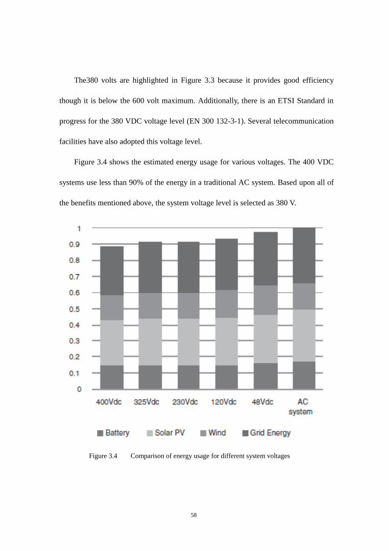
58
The380 volts are highlighted in Figure 3.3 because it provides good efficiency
though it is below the 600 volt maximum. Additionally, there is an ETSI Standard in
progress for the 380 VDC voltage level (EN 300 132-3-1). Several telecommunication
facilities have also adopted this voltage level.
Figure 3.4 shows the estimated energy usage for various voltages. The 400 VDC
systems use less than 90% of the energy in a traditional AC system. Based upon all of
the benefits mentioned above, the system voltage level is selected as 380 V.
Figure 3.4 Comparison of energy usage for different system voltages

59
3.3.2 The Advantages of 380V DC Bus Voltage
Subsequent R&D is able to fully articulate the benefits and advantages of 380 Vdc.
They show that 380 Vdc:
28% more efficient than 208 Vac systems
15% less up-front capital cost in production volumes
33% less floor space
36% lower lifetime cost
20-100 times less copper than -48V DC systems
Higher Reliability:
Higher reliability is the most outstanding advantage of 380 Vdc. By eliminating
the unnecessary conversion architectures, such as the PDUs and transformers, the front
end of the PSU , and in particular, the inverter that is on the output side of the UPS in
the ac design, the reliability of the power delivery chain is improved by 1000%. This
should not come as a surprise because telecommunications companies have been using
-48Vdc systems for decades. In fact, in 2010 when Intel surveyed its manufacturing
organization, it was found that a plenty of critical failures that year was the failures in
the data centers that supported manufacturing [14].
Additionally, the vast majority of these failures were resulted from errors with
manufacturing organization.
Higher Efficiency:

60
380 Vdc is 28% more efficient than the current practice of 208 Vac. The Green
Grid did a peer review of the LBNL findings and concluded that the efficiency findings
were real. The report especially emphasized that if certain techniques be adopted by ac
distribution on 380 Vdc, then the efficiency could be improved by 5–7%. In the Intel,
HP/EY P, and Emerson Network Power study, the improvement of efficiency was
about 7% for dual-corded installations and 8% otherwise compared to 415 Vac. Real
implementations at Duke Energy and Green.ch found 15% and 10% efficiency
improvements, respectively. So an existing legacy data center power distribution
system is replaced, the efficiency gain could be as high as 28%. The gain could be
achieved at least 7–8% for a Greenfield data center, depending on whether it uses a
dual-corded design or not [14].
Lower Cost:
Given that the power distribution system and eliminating components have been
vastly simplified, the cost in volume production is expected to be 15% less. ABB and
Green.ch reported that the cost for the 380-Vdc system built in Zurich in 2010 was 10%
less than for the ac system. (The Green.ch data center has both.)
In fact, lower capital and operating cost are the reasons explaining why 380 Vdc is
the ideal voltage. Another important component in making a cost-effective, efficient
voltage distribution standard is to stay below 420 V so that other parts can share the
volume economics with desktop personal computer PSU s. The final reason of why the

61
industry selected 380 Vdc is because of a specification that requires operation up to
400 Vdc and successful survival when exposure to up to 410 Vdc) [14].
Less Space and Fewer Materials:
The Intel, HP/EY P, and Emerson Network Power study found that the footprint of
the dc power distribution system was 33% smaller than for ac. The power supply was
also reduced 30% by volume due to the elimination of components.
Although this is unlikely to make PSU s smaller since the servers will desire to
use either ac or dc PSU s during the changeover, it will make the 380-Vdc PSU s more
sustainable. They use less of the earth’s resources, and there is less to recycle at the
end of their lives.
With respect to the wiring plant, 380 Vdc uses less copper than ac, even 415 Vac.
Figure 3.5 shows that at the same power conducted, relative conductor diameter for
380V DC uses less copper than even the high-efficiency 415V AC. Conductors for
380V DC are much smaller than -48V DC with much less weight and less copper cost.
Because of skin effect and the reactive current overhead, ac conductors need to be
sized bigger than dc for the same voltage and power capacity. We can see why
telecommunications companies and the island nation of Japan are looking to replace
–48Vdc with 380 Vdc across the board. In fact, some organizations are thinking about
paying for the conversion simply because of the salvage value of the–48Vdc copper
bus bars and conductors that will be replaced.

62
Figure 3.5 Comparison of conductor diameters (courtesy of UECorp) [14]
3.4 PEBB Topology Selection – Bidirectional Dual Active Bridge
3.4.1 The overview of PEBB Topology Candidates
In order to respond to the increasing demand for an intermediate storage of
electrical energy in battery systems as well as the request for using renewable energy,
PEBBs have developed to be able to handle bidirectional power flow and in the same
time provide galvanic isolation. Battery charging systems, photovoltaic equipment and

63
auxiliary power supplies in proposed DC microgrid applications are quintessential
examples that have been created to address these concerns.
Just as mentioned in chapter 2, qualified DC/DC converter candidates of PEBB
should be able to fulfill the requirements of the following general specifications:
Galvanic isolation
Bidirectional power flow ability
High conversion efficiency in the target operating range
Low converter volume
Constant switching frequency
More detailed specifications for the proposed power conversion architecture are
listed in Table 3.3
Table 3.3 Detailed specifications of power converters
Converter
Description
Input Voltage Output Voltage Power (kW)
DC-DC PV 48 VDC 380 VDC (±190 VDC) 2kW
DC-DC Battery 48 VDC 380 VDC (±190 VDC) 2kW(Bidirectional)
AC-DC Wind Based on Power 380 VDC (±190 VDC) 2kW
DC-DC Load Step
Down
380 VDC (±190 VDC) 48 VDC 2kW

64
DC-AC Grid
Connection
380 VDC (±190 VDC) 480 VAC 7.5MW(Total)
From what has shown in Table 3.3, it is not difficult to differentiate the family of
isolated bidirectional DC/DC converter from others having the potential to realize
PEBB concept in the proposed power conversion architecture. The different
components of a bidirectional DC/DC converter with galvanic isolation are depicted in
Figure 3.6.
Figure 3.6 General structure of an isolated, bidirectional DC/DC converter
Different blocks in the diagram represent different components required for an
isolated bidirectional DC/DC converter [50]:
Filter networks provide smooth terminal voltages and current.
DC/AC converter is a switch network which provides AC power to the HF
transformer and the AC/DC converter supplies DC power to the receiving
port; both converters allow for bidirectional power transfer.
Filter
NetworkDC/AC
Resonant
High
Frequency
Network
High
Frequency
Transformer
Resonant
High
Frequency
Network
AC/DCFilter
Network
HighVoltage
Side
Low Voltage
Side
+
-inV
+
-outV

65
The reactive HF networks are used to modify the shapes of the switch
current waveforms in order to achieve low switching losses.
The HF transformer is required in order to achieve electric isolation; it
further enables large voltage and current transfer ratios.(small volume at
HF)
Bidirectional DC/DC converter topologies with a system configuration based on
Figure 3.6, are called Single-Stage Topologies because they contain a minimum
number of conversion stages. Accordingly, the total number of required components is
comparably low.
However, the operation within wide input and output voltage ranges causes
ineffective transformer and switched utilization. Improved transformer and switch
utilization will be achieved with multi-stage topologies, which contain an additional
power converter in order to adjust voltage and current levels [50].
Here, the single-stage topologies are discussed first, and the issue of multi-stage
topologies will be stressed in the following section.
The family tree of the single-stage and two-stage bidirectional and isolated
DC-DC converter topologies are illustrated in Figure 3.7.

66
Figure 3.7 Family tree of single-stage and two-stage bidirectional isolated DC/DC topologies
Bidirectional, two port DC/DC converters with galvanic isolation
Single-Stage Topologies
Basic Single-Stage Converters
Isolated and Bidirectional Flyback
Isolated and Bidirectional Forward
Isolated and Bidirectional Ćuk
Dual Bridge Converters without Resonant Network
Two Voltage Sourced Ports
Single Phase Dual Active Bridge
Three Phase Dual Active Bridge
Voltage and Current Sourced Ports
Voltage sourced full bridge with a current sourced full bridge
Voltage sourced full bridge with a current
doubler
Voltage sourced full bridge with a push-
pull structure
Dual Bridge Converters without Resonant Network
Bidirectional series-parallel resonant LLC
converter
Bidirectional series-parallel resonant LCC
converter
Two-Stage Topologies

67
3.4.2 Single-Stage Topologies
A. Basic single-stage converters
In the family tree of the single-stage bidirectional and isolated DC-DC converter
topologies in Figure 3.7, the first group contains isolated and bidirectional fly back,
forward, and Ćuk converter topologies which are typically employed for applications
with an output power well below 2 kW. Hence, for the proposed PEBB based power
conversion architecture where the modular power rating is 2 kW, the first group of
single stage converters with low numbers of switches is less attractive.
B. Dual Bridge converters without resonant network
The second big branch in the family tree of single stage topologies is the dual
bridge converters without resonant network. There are two subgroups that have been
categorized by the type of voltage source converter or current source converter. One
belongs to the two voltage sourced ports and the other belongs to a mixed voltage and
current sourced ports.
The first category contains a single phase dual active bridge (DAB) converter and
three phase dual active bridges.
The single phase DAB converter is shown in Figure 3.8 and it has the following
characteristics [50]:
Due to the symmetric circuit structure, the DAB readily allows for
bidirectional power transfer.

68
Some other main advantages of the DAB include the low number of
passive components, the evenly shared currents in the switches, and its soft
switching properties. With the DAB converter topology, high power
density is feasible
However, very large low voltage sides RMS capacitor current.
The actual DAB employs full bridge circuits on the HIGH VOLTAGE side
and on the LOW VOLTAGE side. Within the regarded DC/AC converter
topologies (full bridge, half bridge, and push-pull), the full bridge circuits
allow for the best converter utilization.
Figure 3.8 Single phase DAB converter
The three phase DAB converter shown in Figure 3.9 have the following
characteristics [50]:
A low total transformer VA rating, low switch VA ratings and a low
magnetic energy storage capability. In particular, compared to the
single-phase DAB, it has considerably smaller RMS capacitor currents
inV
1T3T
2T4T
+
-
L
5T+
-
outV
6T
7T
8T
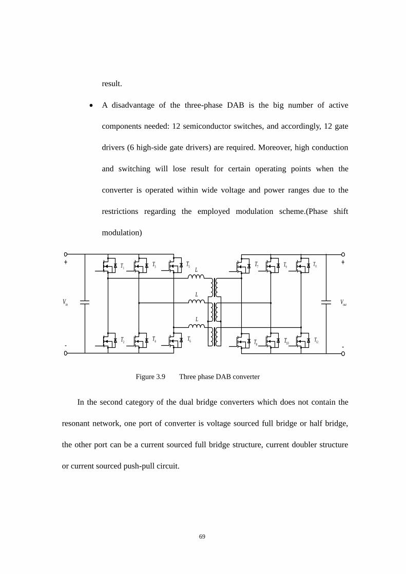
69
result.
A disadvantage of the three-phase DAB is the big number of active
components needed: 12 semiconductor switches, and accordingly, 12 gate
drivers (6 high-side gate drivers) are required. Moreover, high conduction
and switching will lose result for certain operating points when the
converter is operated within wide voltage and power ranges due to the
restrictions regarding the employed modulation scheme.(Phase shift
modulation)
Figure 3.9 Three phase DAB converter
In the second category of the dual bridge converters which does not contain the
resonant network, one port of converter is voltage sourced full bridge or half bridge,
the other port can be a current sourced full bridge structure, current doubler structure
or current sourced push-pull circuit.
inV
1T 3T
2T 4T
+
-
9T
+
-
outV
L
L
L
5T
6T
7T
8T 10T
11T
12T

70
For the bidirectional and isolated full bridge converter in Figure 3.10, though
isolated full bridge converter has the merit of achieving a smooth current and therefore
resulting in a considerably lower capacitor RMS current compared to the DAB, it
needs additional required volume for the DC inductor, and a snubber circuit which
makes this topology less appropriate for the proposed architecture.
Figure 3.10 Voltage sourced full bridge with a current sourced full bridge converter
The bidirectional and isolated full bridge converter with a current doubler on the
low voltage side in Figure 3.11 will lead to an increased transformer VA rating.
Moreover, the current doubler requires two (low-side) switches with a rated voltage of
twice the rated voltage of the full bridge switches, making this topology less favorable
for the proposed architecture.
inV
1T3T
2T4T
+
-
L
5T
+
-
outV
6T
7T
8T
DCL

71
Figure 3.11 Voltage sourced full bridge with a current doubler
The third category is the bidirectional and isolated full bridge converter with a
push-pull structure on low voltage side, which is shown in figure 3.12. However, the
push-pull structure will result in an increased transformer VA rating.
Moreover, each of these windings conducts current only during half a switching
period and consequently, ineffective transformer utilization and the occurrence of a
higher VA rating. Since two (low side) switches with a rated voltage equal to twice the
rated voltage of the full bridge switches are required, this topology seems not to be
perfect for the proposed architecture [50].
Figure 3.12 Voltage sourced full bridge with a push-pull structure on low voltage side
inV
1T3T
2T4T
+
-
L
5T
+
-
outV
6T
1DCL 2DCL
inV
1T3T
2T4T
+
-
L
5T
+
-
outV
6T
DCL

72
C. Dual bridge converters with resonant network
The final big branch on single stage bidirectional and isolated converters is the
family of dual bridge converters with resonant network, which is represented by
series-parallel resonant converters in Figure 3.13 and 3.14. Figure 3.13 demonstrates
the bidirectional series-parallel resonant LLC converter while Figure 3.14 shows the
bidirectional series-parallel resonant LCC converter.
Figure 3.13 Bidirectional series-parallel resonant LLC converter
Figure 3.14 Bidirectional series-parallel resonant LCC converter
It should be noted that the load dependent property of the resonant converters
heavily affects the performance of the dual bridge converters with resonant network,
inV
1T3T
2T4T
+
-
L
5T
+
-
outV
6T
7T
8T
ML
C
inV
1T3T
2T4T
+
-
L
5T
+
-
outV
6T
7T
8T
PC
C

73
therefore making this group less appropriate for applications with large operating
voltage and power ranges or for applications where the converter is most often
operated considerably below its rated power. Moreover, additional hardware is
required to enable bidirectional power flow and frequency control, which is far more
complicated than traditional modulation techniques.
Hence, the family of dual bridge converters with resonant network will not be
considered in the following discussions.
3.4.3 Two-Stage Topologies
The isolated DC/DC converter topologies that have been discussed above are
operated most efficiently if the input to output voltage ratio 𝑉1
𝑉2 is close to the
transformer turns ratio n. Thus, an additional buck or boost converter is employed to
adjust the voltage applied to the isolated DC/DC converter stage, which is also known
as voltage matching [50].
Thus, within the specified input and output voltage ranges, a more evenly
distributed converter efficiency is expected for a two-stage solution which employs an
additional buck and/or boost converter without galvanic isolation to adjust the voltage
applied to the isolated DC/DC converter stage. However, the total number of required
power components is bigger for the two-stage converter. Thus, the additional DC/DC
converter needs to be highly efficient in order to achieve a higher efficiency with the
two-stage converter than with the respective single-stage converter.

74
There are mainly four different arrangements of a bidirectional buck or boost and
a single stage isolated bidirectional DC/DC converter. They are high voltage side buck
converter, high voltage side boost converter, low voltage side buck converter, and low
voltage side boost converter. The high voltage side buck converter is depicted in
Figure 3.15.
Figure 3.15 Two stage converter with buck converter on high voltage side
3.4.4 PEBB Topology Identification
Based on these findings, the single-phase DAB converter topology is considered
to be the most favorable application with respect to its achievable converter efficiency,
the achievable power density due to the low number of inductors, and the employed
capacitive filters on the HIGH VOLTAGE side and on the LOW VOLTAGE side.
In order to compare the efficiencies achieved with the two-stage topologies to the
efficiencies achieved with the single-stage DAB converter, the two most promising
inV
1T
2T
+
-
L
Bidirectional
Isolated
DC/DC
Converter
+
-
outV

75
converter configurations are investigated. However, in average, the additional loss of
the buck-or-boost converter is higher than the loosed reduction achieved so as to the
DAB converter. Hence, the two stage topologies will not be discussed further.
Therefore, the DAB is selected to realize the PEBB concept in proposed power
conversion architecture. Compared to three phase DAB, single phase DAB possess
more merits in modular design, and it will be further discussed in the following
sections.
3.5 Modular Design Considerations
The modular design consideration is the most important advantage of PEBB
concept. Modular design could make PEBBs:
Programmable, extendable, and updatable through software.
Reduce maintenance via plug and play modules.
Reduce cost via increased product development efficiency.
Reduce time to market.
Reduce design and development risk.
Standard PEBB designs cover wider market base.
Same topology for all applications is the key idea in proposed power conversion
architecture. The DAB based upon PEBB converter uses only DAB topology to realize
different application requirements in the system. DC/DC, DC/AC (since the DAB

76
based PEBBs are bidirectional, the DC/AC modal can also be used as AC/DC modular)
and AC/AC are the three types of DAB based on PEBBs, and they are depicted in
Figure 3.16, 3.17 and 3.18 respectively [51].
Figure 3.16 DC/DC PEBB modular
Figure 3.17 AC/DC PEBB modular
inV
1T3T
2T4T
+
-
L
5T
+
-
outV
6T
7T
8T
filterL
filterC

77
Figure 3.18 AC/AC PEBB modular
The function of DC/DC DAB based upon PEBB modular is to regulate the input
and output of solar panels and battery banks for the purpose of maintaining the proper
connection between storage and renewable energy. The function of AC/DC modular is
to regulate the wind power and micro turbines. Moreover, the connection between the
DC bus in the proposed microgrid and AC utility is also ensured by AC/DC modular
[51]. The AC/AC modular is not used in this project; however, it could be used in other
AC microgrid application in the near future.
filterL
filterC
+
-
outV

78
The advantages of modular design include:
Desirable redundancy with increasing reliability.
Same design for all applications shortens the development time.
Same hardware enables fast replacement of broken part which lower
maintance cost.
Programmable, extendable for different applications.
The unified structure will result in a desirable system redundancy without
increasing the cost, since the main cost in renewable energy system is related with the
design and maintained. With the help of modular design, the specified design can be
abolished, for instance, the time and cost for production development for new
application will be significantly shortened. The hardware for different applications is
the same, like the DAB based PEBBs. However, the different functions are achieved
by reprogramed of the controller software. If one part of the converter power circuit is
not working properly, it would not be difficult to replace it, since the hardware is
exactly the same because of the modular design. Hence, the cost of maintains will be
significantly reduced.
When it comes to the broad impact, the solutions for achieving more efficient and
more reliable system architectures and modernized converters for renewable
applications will bring about lower overall costs and greater renewable energy
penetration in the market.

79
The modeling, control and simulations of all types of DAB based PEBBs will be
discussed in detail in the following chapters.

80

81
Chapter 4 Modeling of DAB Based PEBBs
In Section 3.4.4, the single phase DAB converter topology is regarded as the most
promising one among all the topologies with respect to its achievable converter
efficiency and the low converter volume. Moreover, with the advantages of modular
design, the single phase DAB has been identified as the most suitable topology to
realize the PEBB concept in the distributed power conversion architecture for DC
microgrid and integration of renewable energy.
DAB bidirectional DC/DC converter is a topology with the merits of a decreased
number of devices, soft-switching commutations, low cost, and high efficiency. The
use of this topology is proposed for distributed power conversion applications where
the power density, cost, weight, and reliability are critical factors.
In this chapter the steady-state analysis of the single phase and three phase DAB
converter have been carried out. Moreover, the small-signal models of the topologies
have also been developed, providing some guidelines for the controller design.
Simulations results will also be presented to verify the theoretical modeling.

82
4.1 Modeling of DAB based DC/DC PEBBs
4.1.1 Lossless Model of Single Phase DC/DC DAB
Single phase DAB (shown in Figure 4.1) is a bidirectional DC/DC converter
based on two active bridges interfaced through a high-frequency transformer. The
leakage inductance L of the high frequency transformer has a great influence on the
performance of this topology. The symmetrical structure of DAB enables power flow
in both directions in case of the active load.
Figure 4.1 Single phase DC/DC DAB
Under the classical phase shift modulations that will be further discussed in the
following section, each bridge is controlled with constant 0.5 duty cycle to generate a
high-frequency square-wave voltage at its transformer terminals. Considering the
presence of the leakage inductance of the transformer, with a controlled and known
value, the two square waves can be appropriately phase shifted to control the power
ini
inv
outi
outv
P

83
flow from one dc-source to the other, thus bidirectional power transfer can be achieved.
Power is delivered from the bridge which generates the leading square wave [52].
For the simplest electric DAB converter model, assuming low voltage side
quantities are referred to the high voltage side [50]:
All losses are neglected,
The transformer magnetizing inductance and parasitic capacitances are
neglected
𝑉𝑖𝑛 and 𝑉𝑜𝑢𝑡 are treated as constant supplies.
Hence, the resulting lossless DAB model is depicted in Figure 4.2.
Figure 4.2 Single phase DC/DC DAB lossless model
4.1.2 Average Model of Single Phase DC/DC DAB
The average DC/DC DAB model can be written as:
+
-
,sectransformer ondarynV
L+
-
,transformer primaryV

84
1
2
in outd d v vP
fL
(8.1)
1
2
in
out
d d vi
fL
(9.1)
1
2
out
in
d d vi
fL
(10.1)
This average model is used for design control algorithm for DAB converter [52].
If the property of bidirectional power flow is considered, the equation (5.1) ~ (5.3)
should be revised. Equation (5.4) ~ (5.6) provide the revised version.
1
2
in outd d v vP
fL
(5.4)
1
2
in
out
d d vi
fL
(5.5)
1
2
out
in
d d vi
fL
(5.6)
A complete study of the steady-state and the small signal model will be
described in the following sections.
4.1.3 Small Signal Model of Single Phase DC/DC DAB
The small-signal modeling of the DAB converter has been achieved via using the
well-known average techniques described in [9] and [10]. Perturbing equations (8) and

85
(10) of the average output current and the average input current respectively, their
small signal model can be obtained. This model is represented by the following
equations [53],
2
2
1 1 1 11 1
22 2
1
22 2
1 1 2 1
2 2
2 110
22
s s s s
ss
D D Dv
vr C Lf C r C Lf Cv v sv v DD D dv
Lf CLf C RC
(5.4)
The key point of small signal model is the linearization on the operating point;
this can be done by Taylor series expansion.
The small signal models are mainly used to study the dynamic performance and
dynamic stiffness around the specific static operating point.
It should be noted that there are some small differences between the small signal
model derived here and the average model in the last section. These differences are
resulted from the different types of mathematical model: The previous average model
is current type model of DAB, but the small signal model is voltage type model of
DAB, for instance, the state space variable are either current or voltage. If the currents
of high frequency transformer are used as the state variables, a new small signal model
would be derived. In conclusion, they both illustrate the dynamic performance
characteristics of the DAB converter equally.

86
[The Dynamic Model and Hybrid Phase-Shift Control of a Dual-Active-Bridge
Converter]
4.1.4 Three Phase DAB based DC/DC PEBBs
The three phase DC/DC PEBBs is the simple combination of three single phase
DAB. The modeling of three phases DC/DC PEBB is identical to three single phase
DAB.
The control of three phase DAB will be elaborated in the following chapter.
4.2 Modeling of DAB based AC/DC PEBBs
Here in this article, two possible solutions for AC/DC PEBBs are proposed. One is
based on traditional AC/DC converter and the other one is based on AC/DC DAB.
The former one enjoy the advantages of mature topology and control algorithms,
however, this design a little bit violates the principle of modular design, since the DAB
topologies are no longer the only structure in the system. The latter one 100% realize
the modular design consideration, but AC/DC DAB is a relatively new topology, not so
much work had been done. There are still many uncertainty and unknowns of the
characteristics of this type of converter. Moreover, the control technique for this kind
of converter is not fully fledged. There would be some risk, when huge amount of this
kind of converter exist in proposed distributed power conversion architecture.

87
4.2.1 Solution 1: Combination of Traditional AC/DC topology and DC/DC
DAB
The first option is build the AC/DC PEBB via combination of traditional AC/DC
topology and DC/DC DAB. This solution make more sense when three phase PEBBs
are used. The traditional three phase AC/DC converter are shown in Figure 4.3.
Figure 4.3 Traditional three phase AC/DC converter
The mathematical model of the traditional three phase AC/DC converter in da frame is
shown by equation (5.5) and (5.6) [54].
1 0 1 01 1
0 1 0 1
d
qd d
q q d
q
e
ei iR L
i iL R uL L
u
(5.5)
Loadi
CvC
L
ai
aE

88
d d q q Load
dc
dc
u i u i iv
Cv C
(5.6)
It is important to note that the reference voltage in the dq frame should be divide
by half of 𝑉𝑑𝑐 in the controller of traditional three phase AC/DC converter. This
method could prevent the turbulence of DC bus voltage which could influence the AC
side, which will be elaborated in the following sections of control algorithm.
The linearization form of equation (5.5) and (5.6) is the small signal model of
traditional three phase AC/DC converter, as shown by equation (5.7) and (5.8).
1 0 1 01 1
0 1 0 1
d
qd d
q q d
q
e
ei iR L
i iL R uL L
u
(5.7)
d d q q d d q q Load
dc
dc
u i u i u i u i iv
Cv C
(5.8)
It can be seen in the following chapter that the small signal will draw a big
influence on controller design for the traditional three phase AC/DC converter. Since
the control algorithm in dq frame are relatively more complex than the model in
conventional abc frame, special care should be address during the controller design,
this issue will be covered in detail in chapter 5.

89
4.2.2 Solution 2: Pure Single Phase AC/DC DAB
The second option of building AC/DC PEBB is only use single phase AC/DC
DAB as topology candidate. This solution offers a better match of modular design
consideration since the inherent pure DAB module inside the single phase AC/DC
DAB. The single phase AC/DC DAB converter is shown in Figure 4.4. It is obviously
that only one topology is integrated in the proposed converter.
Figure 4.4 Single phase AC/DC DAB
filterL
filterC

90
Just like the three phase DC/DC PEBBs, the three phase AC/DC PEBBs is the
simple combination of three single phase AC/DC DAB. The modeling of three phase
AC/DC PEBB is identical to three single phase AC/DC DAB which is shown clearly in
Figure 4.5.
The control of three phase AC/DC DAB based PEBBs will be elaborated in
chapter 5.
Figure 4.5 Single phase AC/DC DAB based three phase AC/DC PEBB
Single
Phase
AC-DC
DAB

91
Chapter 5 Control Algorithms and Simulation of PEBBs
In Section 3.4.4, the single phase DAB converter topology is regarded as the most
favorable topology with respect to the achievable converter efficiency and with respect
to a low converter volume. Moreover, with the advantages of modular design, the
single phase DAB has been identified as the most suitable topology to realize the
PEBB concept in the distributed power conversion architecture for DC microgrid and
integration of renewable energy.
5.1 Control Method for Single Phase DC/DC DAB
5.1.1 Phase Shift Modulation
The phase shift modulation is the most common modulation principle for DAB
converters. The so called phase shift modulation operates the DAB with a maximum
duty cycles, i.e. D1 = D2 = 0.5, under a constant switching frequency.
The only variable in phase shift modulation controller is the phase shift angle φ
between input side bridge and output side bridge. The phase angle is used to control
the power transfer direction and value. The power always flows from the leading side
to the lagging side of the DAB controller.
92
For the lossless model of the DAB converter, the voltage of both sides of the high
frequency transformer and the leakage inductance current repeat every half-cycle with
reversed signs during the steady state operation.
Since phase shift modulation is a well-developed technique and has been
demonstrated in detail in many publications, it is not elaborated in this article.
The great advantage of the phase shift modulation is its simplicity: only one
control variable in this type of modulation, the phase shift angleφ, is required to adjust
the DAB power level. The simplicity of this modulation method and the possibility of
using half bridge circuits to generate the high frequency transformer voltages are the
main reasons for the wide use of this modulation method.
Disadvantages are a limited operating range with low switching losses, i.e. soft
switching range is limited compared to alternative modulation methods. Moreover,
large RMS currents in the high frequency transformer for most operating points also
causes problem when the DAB is operated in a wide voltage range.
Under phase shift modulation, a special selection of transformer turns ratio and
transformer leakage inductance is the only way to achieve a reduced RMS value of the
transformer current, since it is not possible to modify the shape of the transformer
current, the transformer current waveform solely depends on the DC voltages and on
the phase shiftφ, under the assumption of a constant switching frequency.
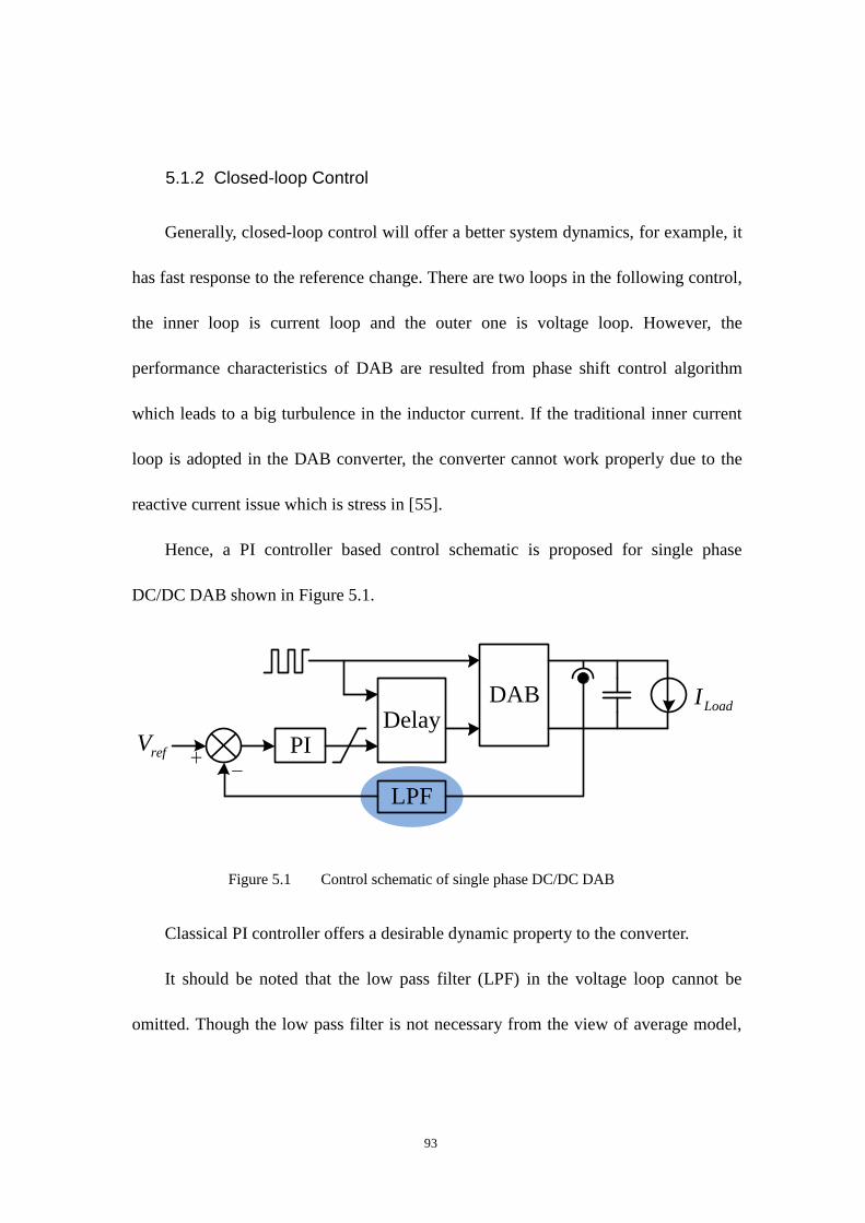
93
5.1.2 Closed-loop Control
Generally, closed-loop control will offer a better system dynamics, for example, it
has fast response to the reference change. There are two loops in the following control,
the inner loop is current loop and the outer one is voltage loop. However, the
performance characteristics of DAB are resulted from phase shift control algorithm
which leads to a big turbulence in the inductor current. If the traditional inner current
loop is adopted in the DAB converter, the converter cannot work properly due to the
reactive current issue which is stress in [55].
Hence, a PI controller based control schematic is proposed for single phase
DC/DC DAB shown in Figure 5.1.
Figure 5.1 Control schematic of single phase DC/DC DAB
Classical PI controller offers a desirable dynamic property to the converter.
It should be noted that the low pass filter (LPF) in the voltage loop cannot be
omitted. Though the low pass filter is not necessary from the view of average model,
-+
PIDelay
DAB
refV
LoadI
LPF

94
the existence of high frequency ripple in the output voltage will result in the instability
of DAB converter.
Generally speaking, the low pass filter limits the band width of the control system,
which will exert a negative influence to the dynamic of the system. Therefore, the
selection of the bandwidth of the low pass filter deserves more attention. In this project,
the second order butterworth low pass filter is selected. The cutoff frequency is chosen
at 0.1~0.2 times of switching frequency.
Base on the discussions above, the control block diagram of the single phase DAB
converter is illustrated in Figure 5.2.
Figure 5.2 Control block diagram of single phase DC/DC DAB
5.2 Control Method for Traditional Three Phase AC/DC Converter
For the traditional three phase AC/DC converter, the most popular control
algorithms are dq frame decouple algorithm and space vector control algorithm. Since
the space vector method is adopted primarily in the application where electrical
-+refV i
p
KK
s
-+
LoadI
1
sCbusV
1
2
ind d v
fL
d
2
2 22s s

95
machine plays a dominant role, the dq frame decouple is selected for this power
conversion architecture. The control block diagram is depicted in Figure 5.3.
It should be noted that the phase angle which is used in park transform and inverse
transform is the phase angle ofeabc. It can be obtained from the phase-locked loop.
Since the converter model is built in dq frame, the controller is also built in the
same frame as the converter, which is shown in Figure 5.4.
It should also be noted that there are block +edq and block of multiply dc voltage
in the diagram of controller, at the same time, the block of −edq and block of divide
dc voltage also exist in the diagram of converter. Hence, they are eliminated in Figure
5.4.
The simulation in the following section shows that this model offers an accurate
estimation of the real system.

96
Figure 5.3 Block diagram of dq frame decouple control for traditional three phase AC/DC converter
PI-
+re
fV
dcv
PI
di 0
qi
PI
+- - -
L
Park
Inve
rse
Tra
ns.
abc
e
2 dcv
abc
m-
+
-+
Cont
roll
erCo
nver
ter
2dcv _
out
abc
u

97
Figure 5.4 Control block diagram of traditional AC/DC converter
PI-
+re
fV
dcv
PI
di 0qi
PI
+- - -
L
-+
-+
1L
1L
+- - -
1s
Load
i
1s
× ×+ +
1C
×÷
-+
1s
dcvL
R R
- -Co
ntro
ller
Conv
erte
r
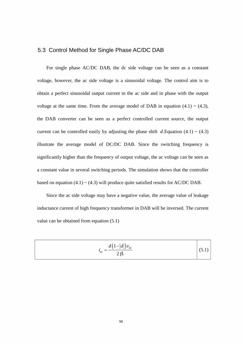
98
5.3 Control Method for Single Phase AC/DC DAB
For single phase AC/DC DAB, the dc side voltage can be seen as a constant
voltage, however, the ac side voltage is a sinusoidal voltage. The control aim is to
obtain a perfect sinusoidal output current in the ac side and in phase with the output
voltage at the same time. From the average model of DAB in equation (4.1) ~ (4.3),
the DAB converter can be seen as a perfect controlled current source, the output
current can be controlled easily by adjusting the phase shift 𝑑.Equation (4.1) ~ (4.3)
illustrate the average model of DC/DC DAB. Since the switching frequency is
significantly higher than the frequency of output voltage, the ac voltage can be seen as
a constant value in several switching periods. The simulation shows that the controller
based on equation (4.1) ~ (4.3) will produce quite satisfied results for AC/DC DAB.
Since the ac side voltage may have a negative value, the average value of leakage
inductance current of high frequency transformer in DAB will be inversed. The current
value can be obtained from equation (5.1)
1
2
dc
ac
d d vi
fL
(5.1)

99
It is obviously that if the output current on the AC side is to be controlled as a
sinusoidal waveform, the 𝑑(1 − |𝑑|) should be sinusoidual. The sign of 𝑑 is
determined by the voltage on ac side.
Assume
(1 ) sin , 0, 0,sin 0d d a t d a t (5.2)
(1 ) sin , 0, 0,sin 0d d a t d a t (5.3)
Since −0.5 < 𝑑 < 0.5, −0.25 < 𝑎 < 0.25. And 𝑎 sin(𝜔𝑡 + 𝜃) should in pahse
with input voltge waveform.
Hence,
1 1 4 sin, sin 0
2
a td a t
(5.4)
1 1 4 sin, sin 0
2
a td a t
(5.5)
The control block diagram is depicted in Figure 5.5.

100
Figure 5.5 Control algorithm of single phase AC/DC DAB
With the help of above control method, the single phase AC/DC DAB model with
controller can be further reduce to Figure 5.6.
Figure 5.6 Block diagram of single phase AC/DC DAB with controller
It should be noted that the instantaneous power on the dc side has a twice line
frequency ripple in single phase DAB, the “third port” method can reduce this kind of
ripple, and it will not be further discussed here.
However, this ripple will not exist in three phase AC/DC DAB, which will be
discussed in the following sections due to the symmetrical three phase voltage.
5.4 Control Method for Three Phase AC/DC DAB
Based on the modular design concerns, three single phase AC/DC DAB
converters are combined in parallel to build three phase AC/DC DAB. The control
-+
PI
LPdcv
refV a
Calculation d
sin t
-+
PI
LP
dcvrefV
sin t
a
acv
1
sC
1
2 fL
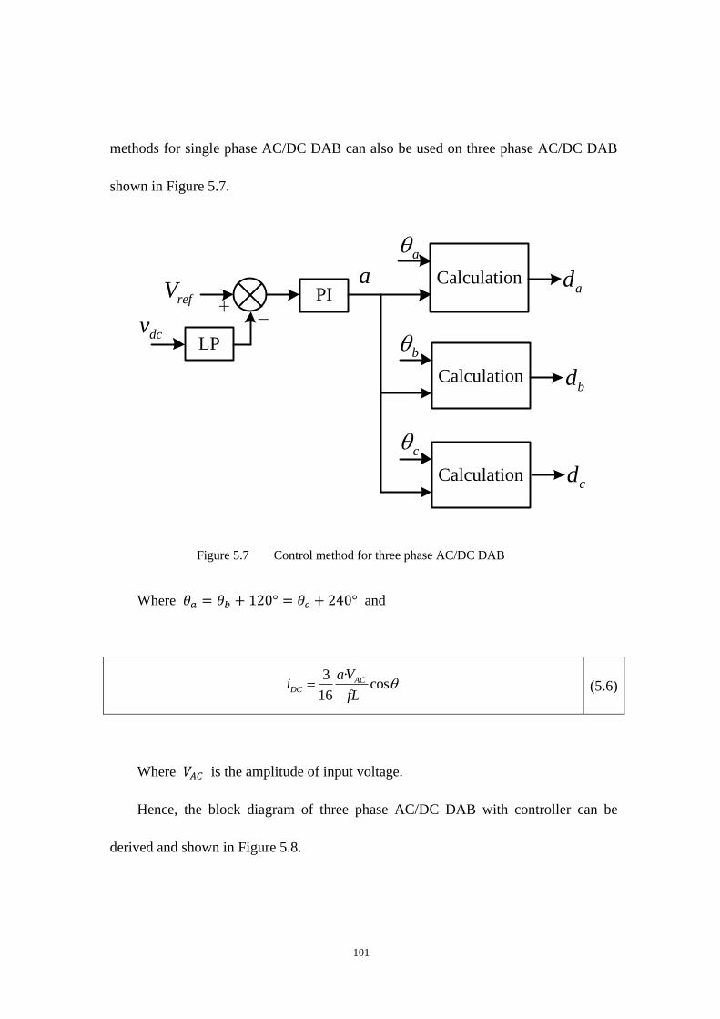
101
methods for single phase AC/DC DAB can also be used on three phase AC/DC DAB
shown in Figure 5.7.
Figure 5.7 Control method for three phase AC/DC DAB
Where 𝜃𝑎 = 𝜃𝑏 + 120° = 𝜃𝑐 + 240° and
·3cos
16
ACDC
aVi
fL (5.6)
Where 𝑉𝐴𝐶 is the amplitude of input voltage.
Hence, the block diagram of three phase AC/DC DAB with controller can be
derived and shown in Figure 5.8.
Calculationada
a
PI
-+refV
LPdcv
Calculationbd
b
Calculationcd
c

102
Figure 5.8 Block diagram of three phase AC/DC DAB with controller
5.5 Simulation Results
5.5.1 Simulation of DC/DC Single Phase DAB
The Simulink model of the single phase DC/DC DAB based PEBB is shown in
Figure 5.9. The realization of phase shift modulation of DC/DC DAB is illustrated by
Figure 5.10.
Figure 5.10 shows that the phase shift modulation signals are obtained by
waveform comparison. The phase shift angle φ is calculated by the outside loop and
feedforward into the phase shift modulation signals generator.
The overall system is depicted in the Figure 5.11. The power circuit of the DAB
converter, current source and load are in the upper part of Figure 5.11. It should be
noted that, there are two intended step change for source and load. These two step
changes are used for testing the dynamic response of the converter.
-+
PI
LP
dcvrefVa
acV
1
sC
3cos
16
ACa V
fL

103
Figure 5.9 Simulink model of single phase DC/DC DAB based PEBB
Figure 5.10 Simulink model of phase shift modulation signal generator for DC/DC DAB
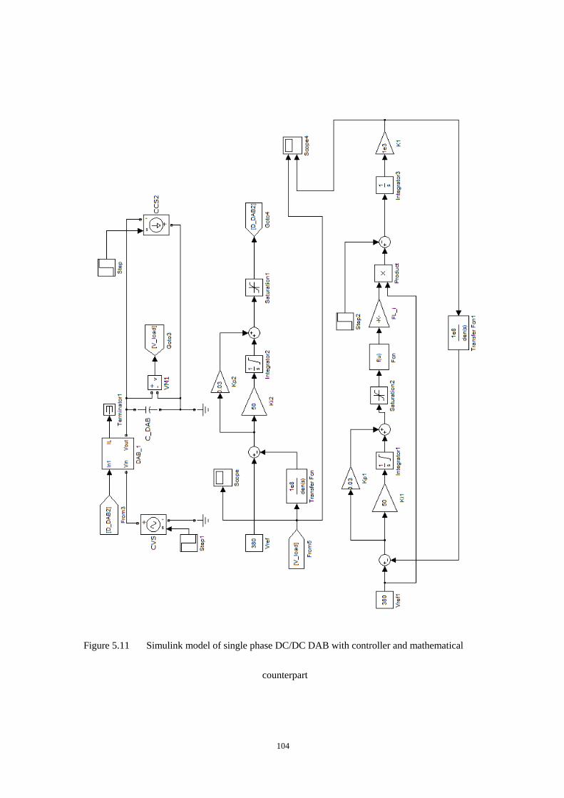
104
Figure 5.11 Simulink model of single phase DC/DC DAB with controller and mathematical
counterpart

105
The controller of DAB is in the middle part of the picture, the phase shift angle φ
is calculated based on the mathematical relationship between phase shift angle φ and
power transferred from the leading side to the lagging side.
In order to compare the performance of detailed real switched based model shown
in Figure 5.9 to the theoretical mathematical linearized DAB and controller model, the
mathematical counterpart of the real switched based model is built at the bottom of
Figure 5.11. The comparison of simulation results are shown in Figure 5.12.
It can be seen easily that the output voltage waveforms of detailed model and the
mathematical linearized model are 100% identical in the Figure 5.12, which verifies
that the controller works properly and the linearized model has achieved a very
accurate estimation of the behavior of real system.
It should be noted that there are step changes at 0.1s for load and source, which is
shown as the small sag in Figure 5.12 and the zoomed view is shown in Figure 5.13.
Moreover, the dynamic responses of the starting period are also shown in detailed in
Figure 5.14.
The identical dynamic responses of both models verify the model and proposed
control theory again. And the switching frequency voltage ripples shown in each upper
waveform of Figure 5.13 and Figure 5.14 are caused by the switch characteristic in the
detailed real switch based model.

106
Figure 5.12 Simulation result of output voltages of detailed DAB model and linearized model

107
Figure 5.13 Detailed view of output voltages of DC/DC DAB during source and load disturbance
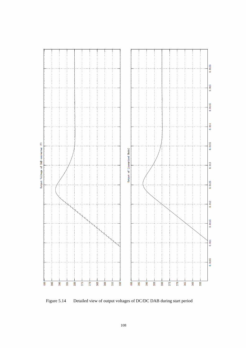
108
Figure 5.14 Detailed view of output voltages of DC/DC DAB during start period

109
5.5.2 Simulation of AC/DC Single Phase DAB
The phase shift modulation signals of AC/DC single phase DAB are obtained by
exactly same way compared to DC/DC phase shift modulation signal generator. The
algorithm for obtaining d is shown in Figure 5.15.
Figure 5.15 Algorithm for obtaining d for AC/DC DAB
The Simulink model of the single phase AC/DC DAB based PEBB and the
realization of phase shift modulation of AC/DC DAB is shown in Figure 5.16.
The overall system is depicted in the Figure 5.17. The power circuit of the AC/DC
DAB converter, AC voltage source and load are in the upper part of Figure 5.17.
The capacitor voltage and inductor current of the LC filter are shown in Figure
5.18. It can be seen that the controller works properly to get a sinusoidal waveform.
The switching frequency ripple will decay continuously when system keeps going to
steady state operation.

110
Figure 5.16 Simulink model of single phase AC/DC DAB based PEBB and phase shift modulation
signal generator

111
Figure 5.17 Simulink model of phase shift modulation signal generator for DC/DC DAB

112
Figure 5.18 Waveform of LC filter

113
5.5.3 Simulation of Traditional Three Phase AC/DC Converter
The Simulink model of the traditional three phase AC/DC converter is shown in
Figure 5.19.
Figure 5.19 Simulink model of traditional three phase AC/DC converter

114
The mathematical model of traditional three phase AC/DC converter and
controller is shown in Figure 5.20.
Figure 5.20 Mathematical model of traditional three phase AC/DC converter
The mathematical model of the controller of traditional three phase AC/DC
converter is shown in Figure 5.21
Figure 5.21 Mathematical model of the controller traditional three phase AC/DC converter

115
The overall system is depicted in the Figure 5.22 and Figure 5.23. The power
circuit of the traditional three phase AC/DC converter and mathematical theoretical
model are in the first part. The controller is depicted in the second part.
It should be noted that, the park transformation in both Figure 5.22 and Figure
5.23 are based on the control algorithm in dq frame which has been illustrated in the
previous section.
The comparison of simulation results of DC voltage of real switch based model
(upper one) and mathematical model (lower one) are shown in Figure 5.24.
It can be seen that the output voltage waveforms of detailed model and the
mathematical linearized model are similar in the Figure 5.24, which verifies that the
controller works properly and the linearized model has achieved a very accurate
estimation of the behavior of real system.
It should be noted that the zoom view of the small sag is shown in Figure 5.25 and
the zoomed view of starting performance is shown in Figure 5.26. The same dynamic
responses of both models verify the model and proposed control theory again.
For the same story, the current of both detailed model and the mathematical
linearized model in dq frame are compared to verify the controller and modeling. The
waveforms are shown in Figure 5.27 and the zoomed version under load turbulence
and startup are shown in figure 5.28 and Figure 5.29. Same results are expected, the
model follow the real system nearly perfect.

116
Figure 5.22 Traditional three phase AC/DC converter with controller and mathematical counterpart
(part 1)

117
Figure 5.23 Traditional three phase AC/DC converter with controller and mathematical counterpart
(part 2)

118
Figure 5.24 Simulation result of output voltages of detailed traditional three phase AC/DC converter
model and linearized model

119
Figure 5.25 Detailed view of output voltages of detailed traditional three phase AC/DC converter
model and linearized model during disturbance
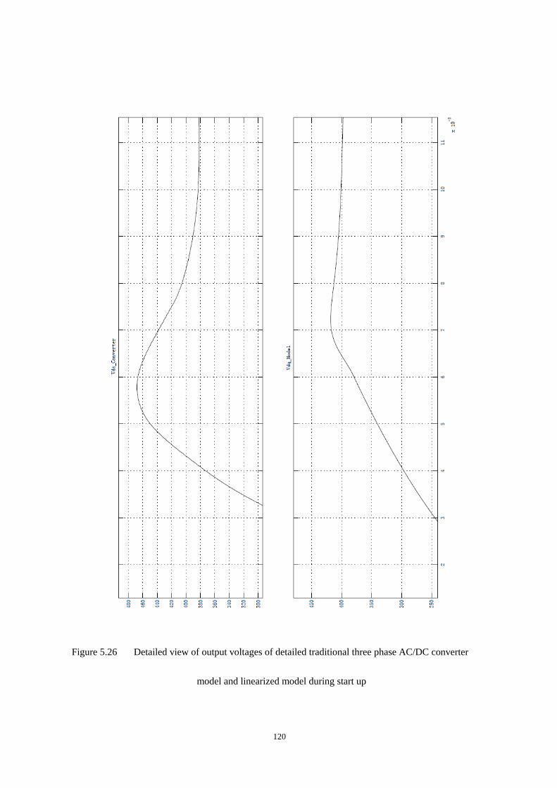
120
Figure 5.26 Detailed view of output voltages of detailed traditional three phase AC/DC converter
model and linearized model during start up

121
Figure 5.27 Simulation result of dq current of detailed traditional three phase AC/DC converter
model and linearized model

122
Figure 5.28 Detailed view of dq current of detailed traditional three phase AC/DC converter model
and linearized model during disturbance
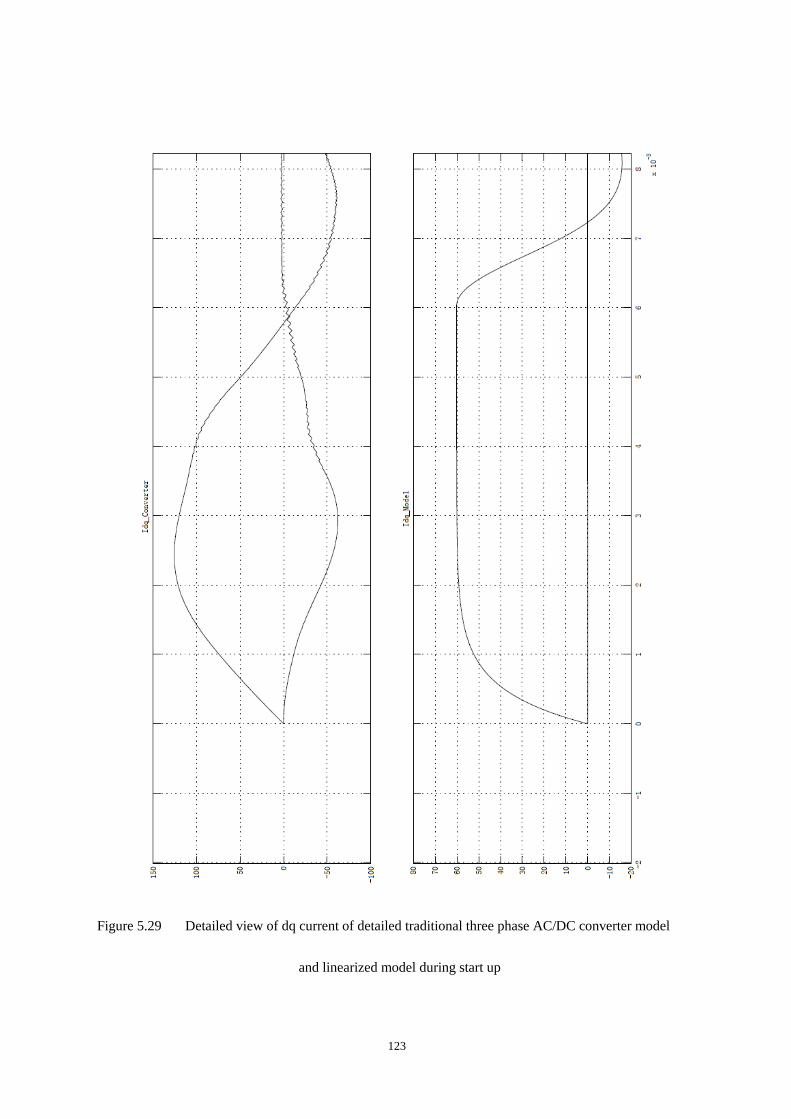
123
Figure 5.29 Detailed view of dq current of detailed traditional three phase AC/DC converter model
and linearized model during start up

124
5.5.4 Simulation of Three Phase AC/DC DAB
The Simulink model of the three phase AC/DC DAB with controller is shown in
Figure 5.30.
The comparison of simulation results of DC voltage of real switch based model
(upper one) and mathematical model (lower one) are shown in Figure 5.31.
It can be seen that the output voltage waveforms of detailed model and the
mathematical linearized model are similar in the Figure 5.31, which verifies that the
controller works properly and the linearized model has achieved a very accurate
estimation of the behavior of real system.
It should be noted that the zoom view of the small sag is shown in Figure 5.32 and
the zoomed view of starting performance is shown in Figure 5.33. The same dynamic
responses of both models verify the model and proposed control theory again.
The voltage and current waveforms after the special designed low pass filter are
also being examed. The simulation results are shown in Figure 5.34. Figure 5.34
illustrates that the low pass filter is well design and desired voltage and current
waveforms are obtained.
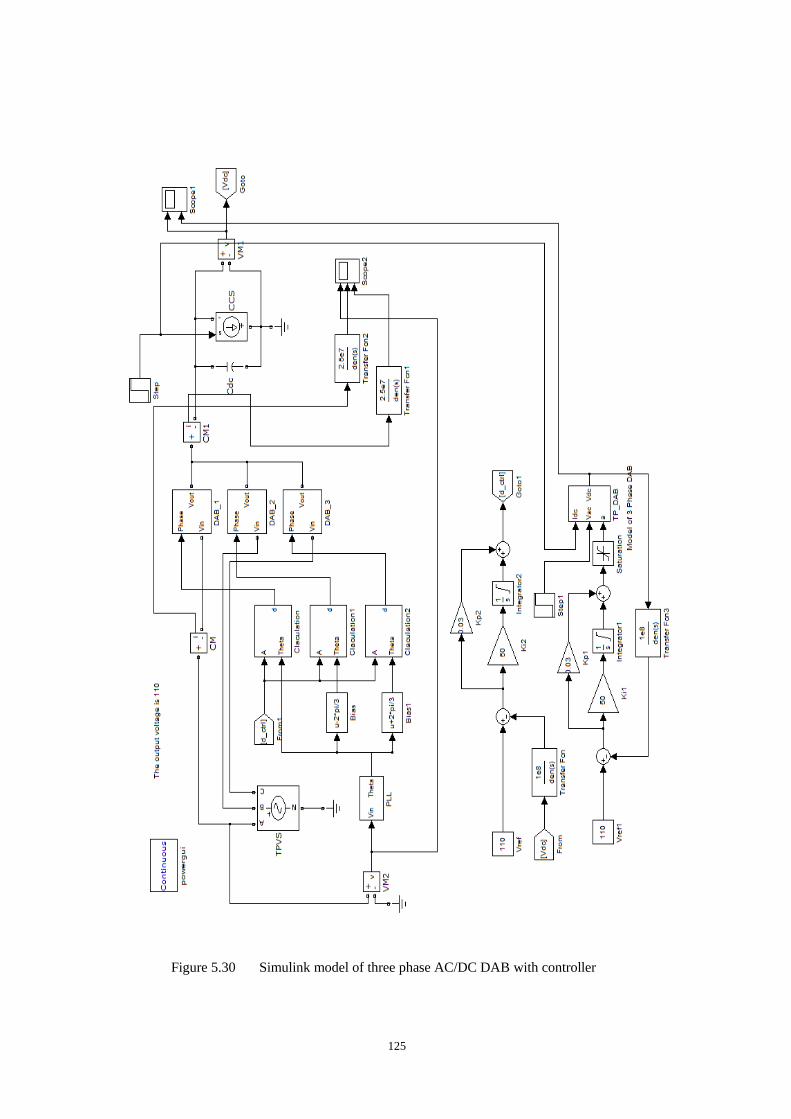
125
Figure 5.30 Simulink model of three phase AC/DC DAB with controller

126
Figure 5.31 Simulation result of output voltages of detailed three phase AC/DC DAB model and
linearized model

127
Figure 5.32 Detailed view of output voltages of detailed three phase AC/DC DAB model and
linearized model during disturbance

128
Figure 5.33 Detailed view of output voltages of detailed three phase AC/DC DAB model and
linearized model during start up

129
Figure 5.34 Voltage and current waveforms after low-pass filter

130

131
Chapter 6 Conclusion and Future Work
The three main objectives of this project is to propose new distributed power
conversion architecture for microgrid and integration of renewable energy sources; to
identify proper topology for realizing DC/DC and AC/DC PEBB concept, and to
develop suitable converter models and control algorithms for microgrid system
simulation.
It has been approved that the proposed the distributed power conversion
architecture enjoys far more advantages than traditional power conversion architecture,
such as higher reliability, higher efficiency and lower cost. Moreover, the DAB based
PEBBS would enable the modular design in the proposed distributed architecture,
which offers the ability to be reprogrammable and extendable for different applications.
Modular design can also reduce maintenance cost by plug-and play and standard
design.
Three challenges remain for future research. Firstly, since this research is an
entirely theoretical study of the characteristics of distributed power conversion
architecture for microgrid and integration of renewable energy sources from the view
of power electronics converter, in which many parameters’ non-linearity and other

132
detailed performance of converter have not been taken into consideration; for the
future work, more detailed model of all types of PEBBs definitely deserves more
attention. In a practical manner, I would suggest taking the first step to build a
prototype of the PEBBs; and then to consider the more complicated characteristics of
the PEBBs, especially the AC/DC PEBB.
Secondly, it is desirable to develop a whole novel system that minimizes the loss
control. The traditional phase shift modulation control algorithm do not offer an
optimized operating point for the PEBB converter, the soft switching range is limited
by phase shift modulation. Due to the modular design consideration, DAB topology is
the only structure in the proposed system. If each modular suffers from the softs
witching problem, the system cannot operating in a big range of operating conditions.
The losses of other parts of the system, for example, thermal losses, have not being
taken into account. Hence, there is a high likelihood to develop a
whole-system-loss-minimize-control algorithm that examines the big picture of overall
efficiency.
Finally, a perfect way to figure out how to combine PEBBs would be to achieve
the goal of optimizing the whole power conversion architecture.
133
References
[1] L. L. Lai and T. F. Chan, “Distributed Generation: Induction and Permanent
Magnet Generators”, Wiley, 2007
[2] Steven Fredette, “Squirrel cage induction machines in distributed generation and
microgrids”, Ph.D Thesis, University of Wisconsin-Madison, 2009.
[3] “Impact of the financial crisis on carbon economics, viersion 2.1 of the global
greenhouse gas abatement cost curve.”, Executive Report, McKinsey &
Company, December 2010.
[4] N. W. A. Lidula, A. D. Rajapakse, “Microgrids research: A review of
experimental microgrids and test systems”, Renewable and Sustainable Energy
Reviews, 15 (2011) pp. 186-202
[5] Sels T, Dragu C, Van Craenenbroeck T, Belmans R. Electrical energy storage
systems: existing systems versus newest systems—an overview. In: Power
generation and stainable development international conference.2001. p. 215–
20.
[6] E.A. Technology. Review of Electrical Energy Storage Technologies and
Systems and of their Potential for the UK. DTI 2004. URN 04/1876.
[7] Kroposki B, Lasseter R, Ise T, Morozumi S, Papatlianassiou S, Hatziargyriou N.
A look at microgrid technologies and testing projects from around the world,

134
Making Microgrids work. IEEE Power Energy Magazine 2008; May/June: 40–
53.
[8] Katiraei F, Iravani R, Hatziargyriou N, Dimeas A. Microgrids management:
controls and operation aspects of microgrids. IEEE Power Energy Magazine
2008; May/June: 54–65.
[9] DTI. Micro-generation strategy and low carbon buildings programme–
consultation. June 2005.
[10] Driesen J, Katiraei F. Design for distributed energy resources. IEEE Power
Energy Magazine 2008; (May/June):30–40.
[11] “Integration of Distributed Energy Resources, The CERTS Microgrid
Concept”, Consultant Report, Oct. 2003.
[12] R. H. Lasseter, “Microgrids and ditributed generation,” in Journal of Energy
Engineering., American Society of Civil Engineerings, Sept. 2007.
[13] Venkataramanan, G., Illindala, M. S., Houle, C., Lasseter, R. H. (2002).
Hardware Development of a Laboratory-Scale Microgrid Phase 1: Single
Inverter in Island Mode Operation. NREL Report No. SR-560-32527 Golden,
CO: National Renewable Energy Laboratory.
[14] G. AlLee and W. Tschudi, “Edison Redux”, IEEE Power and Energy Magazine,
Nov. Dec. 2012.
[15] X. Liu, P. Wang, P. C. Loh, “A hybrid AC/DC Micro-grid” , IPEC, 2010
Conference Proceedings, pp.467-451.

135
[16] R. H. Lasseter, “MicroGrids,” in Power Engineering Society Winter Meeting,
2002. IEEE, 2002, pp.305-308 vo1.1. (2.13)
[17] Y. Zoka, H. Sasaki, N. Yorino, K. Kawahara, and C. C. Liu, “An interaction
problem of distributed generators installed in a MicroGrid,” in Electric Utility
Deregulation, Restructuring and Power Technologies, 2004. (DRPT 2004).
Proceedings of the 2004 IEEE International Conference on, 2004, pp. 795-799
Vol.2.
[18] R. H. Lasseter and P. Paigi, “Microgrid: a conceptual solution,” in Power
Electronics Specialists Conference, 2004. PESC 04. 004 IEEE 35th Annual,
2004, pp. 4285-4290 vol.6.
[19] M. E. Baran and N. R. Mahajan, “DC distribution for industrial systems:
Opportunities and challenges,” IEEE Transactions on Industry Applications, vol.
39, pp. 1596-1601, 2003.
[20] D. J. Hammerstrom, “AC versus DC distribution systems-did we get it right?” in
2007 IEEE Power Engineering Society General Meeting, PES, 2007.
[21] Y. M. Chen, C. S. Cheng, and H. C. Wu, “Grid-connected hybrid PV/Wind
power generation system with improved DC bus voltage regulation strategy,” in
Conference Proceedings - IEEE Applied Power Electronics Conference and
Exposition - APEC, 2006, pp. 1088-1094.
[22] P. C. Loh, D. Li, Y. K. Chai and F. Blaabjerg, “Autonomous operation of hybrid
microgrid with AC and DC subgrids” , IEEE Transactions onPower Electronics,
vol. 28, no. 5, pp. 2214-2223, May 2013.

136
[23] P. Chiradeja and R. Ramakumar, “An approach to quantify the technical benefits
of distributed generation,” IEEE Trans. Energy Convers., vol. 19, no. 4, pp. 764–
773, Dec. 2004.
[24] R. C. Dugan and T. E. McDermott, “Distributed generation,” IEEE Ind. Appl.
Mag., vol. 8, pp. 19–25, Mar./Apr. 2002.
[25] R. H. Lasseter and P. Paigi, “Microgrid: A conceptual solution,” in Proc. IEEE
Power Electron. Spec. Conf., Jun. 2004, pp. 4285–4290.
[26] H. Nikkhajoei and R. H. Lasseter, “Distributed generation interface to the
CERTS microgrid,” IEEE Trans. Power Del., vol. 24, no. 3, pp. 1598– 1608, Jul.
2009.
[27] J. M. Guerrero, J. C. Vasquez, J. Matas, L. G. de Vicuna, and M. Castilla,
“Hierarchical control of droop-controlled ac and dc microgrids—A general
approach toward standardization,” IEEE Trans. Ind. Electron., vol. 58, no. 1, pp.
158–172, Jan. 2011.
[28] J. M. Guerrero, L. Hang, and J. Uceda, “Control of distributed uninterruptible
power supply systems,” IEEE Trans. Ind. Electron., vol. 55, no. 8, pp. 2845–
2859, Aug. 2008.
[29] K. D. Brabandere, B. Bolsens, J. V. D. Keybus, A. Woyte, J. Driesen, and R.
Belmans, “A voltage and frequency droop control method for parallel inverters,”
IEEE Trans. Power Electron., vol. 22, no. 4, pp. 1107–1115, Jul. 2007.

137
[30] M. Prodanovic and T. C. Green, “High-quality power generation through
distributed control of a power parkmicrogrid,” IEEE Trans. Ind. Electron., vol.
53, no. 5, pp. 1471–1482, Oct. 2006.
[31] M. N. Marwali, J. W. Jung, and A. Keyhani, “Control of distributed generation
systems: Part II. Load sharing control,” IEEE Trans. Power Electron., vol. 19,
no. 6, pp. 1551–1561, Nov. 2004.
[32] T. L. Lee and P. T. Cheng, “Design of a new cooperative harmonic filtering
strategy for distributed generation interface converters in an islanding network,”
IEEE Trans. Power Electron., vol. 22, no. 5, pp. 1919–1927, Sep. 2007.
[33] R. Majumder, A. Ghosh, G. Ledwich, and F. Zare, “Load sharing and power
quality enhanced operation of a distributed microgrid,” IET Renew. Power
Gener., vol. 3, no. 2, pp. 109–119, Jun. 2009.
[34] A. Tuladhar, H. Jin, T. Unger, and K.Mauch, “Control of parallel inverters in
distributed ac power systems with consideration of line impedance effect,” IEEE
Trans. Ind. Appl., vol. 36, no. 1, pp. 131–137, Jan./Feb. 2000.
[35] J. M. Guerrero, L. G. Vicu˜na, J. Matas, M. Castilla, and J. Miret, “Output
impedance design of parallel-connected UPS inverters with wireless loadsharing
control,” IEEE Trans. Ind. Electron., vol. 52, no. 4, pp. 1126–1135, Aug. 2005.
[36] R. Majumder, B. Chaudhuri, A. Ghosh, R. Majumder, G. Ledwich, and F. Zare,
“Improvement of stability and load sharing in an autonomous microgrid using
supplementary droop control loop,” IEEE Trans. Power Sys., vol. 25, no. 2, pp.
796–808, Jul. 2010.

138
[37] Y. Mohamed and E. F. El-Saadany, “Adaptive decentralized droop controller to
preserve power sharing stability of paralleled inverters in distributed generation
microgrids,” IEEE Trans. Power Electron., vol. 23, no. 6, pp. 2806–2816, Nov.
2008.
[38] B. K. Johnson, R. H. Lasseter, F. L. Alvarado, and R. Adapa, “Expandable
multiterminal dc systems based on voltage droop,” IEEE Trans. Power Del., vol.
8, no. 4, pp. 1926–1932, Oct. 1993.
[39] T. Ericsen, “Power Electronics Building Blocks – a Systematic Approach to
Power Electronics”, Power Engineering Society Summer Meeting, Machine
and Drives, 2000, pp. 1216-1218, vol. 2.
[40] T. Ericsen, N. Hingorani, Y. Khersonsky, “PEBB – Power Electronics Building
Blocks From Concept to Reality”, The 3rd
IET International Conference on
Power Electronics, Machine and Drives, 2006, pp. 12-16.
[41] T. Ericsen, “Power Electronics Building Blocks”, Electric Warship Conference,
IME/IEE/SEE, London, 1997.
[42] Power Electronics Building Block (PEBB) Concepts", IEEE publication 04TPI
70 prepared by the Task Force 2 of the working Group i8, 2004
[43] S. Kjaer, J. Pedersen, and F. Blaabjerg, “A review of single-phase
grid-connected inverters for photovoltaic modules,” IEEE Trans. Industry App.,
vol. 41, no. 5, Sept./Oct. 2005.
[44] D. Morrison, “Distributed power architectures evolve and reconfigure,” Power
Electronics Technology, May 2004.

139
[45] R. White, “Emerging on-board power architectures,” IEEE Applied Power
Electron. Conf., vol. 2, pp. 799-804, Feb. 2003.
[46] F. Lee, S. Wang, P. Kong, C. Wang, D. Fu, “Power architecture design with
improved system efficiency, EMI and power density,” IEEE Power Electronics
Specialists Conference, pp. 4131-4137, June 2008.
[47] R. Lasseter, “MicroGrids,” IEEE Power Engineering Society Winter Meeting,
vol. 1, pp. 305-308, 2002.
[48] B. Kroposki, R. Lasseter, T. Ise, S. Morozumi, S. Papatlianassiou, and N.
Hatziagyriou, Making microgrids work,” IEEE Power and Energy Magazine,
vol. 6, iss. 3, pp. 40-53, May-June 2008.
[49] N. Hatziargyriou, H. Asano, R. Iravani, and C. Marnay, “Microgrids,” IEEE
Power and Energy Magazine, vol. 5, iss. 4, pp. 78-94, Jul. 2007.
[50] Florian Krismer, “Modeling and Optimization of Bidirectional Dual Active
Bridge DC/DC Converter Topologies”, Ph.D Thesis, ETH Zurish, 2010.
[51] Hengsi Qin, “Dual active bridgeconverters in solid state transformers”, Ph.D
Thesis, Missouri University of Science and Technology, 2012.
[52] A.R. Alonso, J. Sebastian, D.G. Lamar, M.M. Hernando and A. Vazquez, “An
overall study of a Dual Active Bridge for bidirectional DC/DC conversion” ,
Energy Conversion Congress and Exposition (ECCE) , 2010, pp. 1129-1135
[53] H. Bai, C. Mi, C. Wang, S. Gargies, “The Dynamic Model and Hybrid
Phase-Shift Control of a Dual-Active-Bridge Converter”, IEEE 34th Annual
Conference of Industrial Electronics (IECON), 2008.

140
[54] P. Rioual, H. Pouliguen, J. Louis, “Regulation of a PWM Rectifier in the
Unbalanced Network State Using a Generalized Model”, IEEE Transactions on
Power Electronics. Vol. 11, issue 3, 1996, pp. 495-502
[55] H. Qing and J. W. Kimball, “Closed-loop Control of DC-DC Dual Active
Bridge Converters Driving Single-Phase Inverters” ,Energy Conversion
Congress and Exposition (ECCE) , 2012, pp. 173-197