Embed Size (px)
Citation preview

J Nanostruct 7(4): 309-322, Autumn 2017
RESEARCH PAPER
DMMP Sensing Performance of Undoped and Al Doped Nanocrystalline ZnO Thin Films Prepared by Ultrasonic Atomization and Pyrolysis MethodShanabhau Damu Bagul, Dhanashree Gajanan Patil and Lalchand Avachit Patil*
Nanomaterial Research Laboratory, Department of Physics, Pratap College Amalner, Jalgaon, India
* Corresponding Author Email: [email protected]
ARTICLE INFO
Article History:Received 07 August 2017Accepted 15 September 2017 Published 01 October 2017
Keywords:Al dopingDMMP gas sensorsNanocrystalline thin filmsSimulantsUltrasonic atomization and pyrolysisZinc oxide
ABSTRACT
How to cite this articleBagul S. D, Patil D. G, Patil L. A. DMMP Sensing Performance of Undoped and Al Doped Nanocrystalline ZnO Thin Films Prepared by Ultrasonic Atomization and Pyrolysis Method. J Nanostruct, 2017; 7(4):309-322.
Highly textured undoped (pure) and Al doped ZnO nanocrystalline thin films prepared by ultrasonic atomization and pyrolysis method are reported in this paper. ZnCl2 water solution was converted into fine mist by ultrasonic atomizer (Gapusol 9001 RBI Meylan, France). The mist was pyrolyzed on the glass substrates in horizontal quartz reactor placed in furnace. The Structural and microstructural properties of the films were characterized by X-Ray Diffractometer (XRD), Field Emission Scanning Electron Microscopy (FESEM) and Transmission Electron Microscopy (TEM). FESEM and TEM analysis revealed that the ZnO thin films prepared were porous monodisperse and nanocrystalline in nature, with average particle size of 15 nm. The optical properties of thin films were characterized by UV-Visible and Photoluminescence (PL) spectroscopy. The films were cut in typical size and electrical contactswere made using silver paste and copper wires. The thin film based sensors so prepared were tested on exposing the simulants of chemical warfare agent (CWA) like: DMMP, CEES and CEPS. Sensors showed better response to DMMP (a simulant of sarin gas) as compared with its responses to CEES and CEPS. Al (1 at%) doped ZnO thin film based sensor showed highest response to DMMP (2 ppm). The simulant response, selectivity and response-recovery time of the sensors were measured and presented. The role of Al dopant in ZnO to enhance DMMP response is discussed.
INTRODUCTION There is an urgent need for detectors and sensors
that are able to warn about imminent chemical warfare agents (CWAs) danger, to enable people to safely leave a contaminated zone or to protect themselves. Accordingly, highly selective sensitive sensors to CWAs have to be the primary focus, i.e. they have to respond to low concentrations of agents—considerably lower than immediately dangerous to life or health concentrations (IDLH). They also have to detect CWAs on the other chemicals’ background and in the environment [1,
2]. The uses of CWAs for research are restricted because they are highly toxic. The research is carried out on chemicals which have similar chemical properties as like CWAs but they are non-toxic called as simulant compounds [3-5]. Although a number of compounds have been used as CWA simulants, no individual compound is ideal because a single simulant cannot satisfactorily represent all environmental properties of a given CWA. Thus a number of different chemicals have been used as simulants of CWA depending on their physical and chemical properties of interest.
This work is licensed under the Creative Commons Attribution 4.0 International License.To view a copy of this license, visit http://creativecommons.org/licenses/by/4.0/.

310
L. A Patil et al/ DMMP Sensing Performance of ZnO Thin Films
J Nanostruct 7(4): 309-322, Autumn 2017
2-Chloroethyl ethyl sulfide (2-CEES, C4H9ClS) and 2-chloroethyl phenyl sulfide (CEPS, C8H9ClS) are the simulants of sulfur mustard and dimethyl methyl phosphonate (DMMP, C3H9O3P) is the simulant of sarin, etc. Our main interest is to develop the semiconducting metal oxides (SMO) based sensors to detect the sarin gas which is too toxic to handle. We, therefore, have to make investigations on the simulant of sarin gas, that is, DMMP.
Now days, there are several techniques and analytical methods used to detect the CWA [6-23]. Metal oxide semiconductor (MOS) gas sensor, as one of the most important conductometric sensors, has attracted dramatic attentions due to their numerous positive features [24, 25]. Chemiresistive sensors offer a wide variety of advantages over other analytical instruments such as low cost, short response time, easy manufacturing, and small size.
In nanoparticulate materials, the enhanced surface area and interconnected particles give rise to a large number of energy traps on the surface and grain boundaries [26-29]. Research into thermally driven heterogeneous reactions on nanoparticulate metal-oxide surfaces is of fundamental importance in the development of new materials for chemical catalysis, including the decontamination of chemical warfare agents (CWAs) [30]. Activation of lattice oxygen from semiconductor oxides is the key step in the mechanism that drives the thermal decomposition of a variety of organic adsorbates, including CWAs, in the absence of gas phase oxygen [31-36]. Doping is another effective and simple way to improve the gas sensing performance of the sensor by increasing the response, selectivity and stability. Effect of doping also reduces the operating temperature and decreases the response-recovering times [37-42].
Ultrasonic atomization and pyrolysis technique for thin film preparation is easier to produce highly textured porous thin films, requiring no vacuum for processing than other coating methods. Additionally, this coating technique features the ability to control desired morphology characteristics. Uniform, thin, well textured and crack free thin films with high transmittance and conductive properties are possible using coating by pyrolysis. The technique used here produces highly uniform film because the pressure inside the quartz reactor furnace is maintained by the trap system at rear end. Mist of the solution is
flowed uniformly on the surface of the substrates which are placed inside the quartz reactor at particular temperature.
There are few reports on nanocrystalline Al-doped ZnO thin film based sensors to detect DMMP simulant. Pure and Al doped nanocrystalline ZnO thin films were therefore prepared by ultrasonic atomization and pyrolysis technique. Sensors were fabricated from the prepared thin films and the sensing performance was studied on exposure of DMMP, CEES and CEPS simulants in this work.
MATERIALS AND METHODSUltrasonic atomization and pyrolysis system
The ultrasonic atomization and pyrolysis system is shown in Fig.1. It consists of ultrasonic atomizer (Gapusol 9001 RBI Meylan, France with frequency of 2.1-2.3MHz), double zone quartz reactor, furnace, thermocouple with temperature indicator and trap system. Ultrasonic generator produces high frequency waves having frequency of 2.1-2.3MHz. This high frequency signal is supplied to piezoelectric transducers. The transducers convert a high frequency into mechanical energy. This energy is used to convert the precursor solution into the fine mist or smoke. The mist is pushed into the quartz reactor placed into horizontal furnace by air compressor connected to chamber of ultrasonic generator. The mistwas pyrolyzed onto the previously kept glass substrates in horizontal furnace.
Preparation of undoped ZnO thin filmsUltrasonic atomization and pyrolysis technique
(Fig. 1) was used to prepare highly textured pure (undoped) and Al doped nanocrystalline ZnO thin films. ZnCl2 solution (300 ml) of 0.05M was prepared in double distilled water and 0.1 ml HCl was added to get clear solution. This stock solution was stored into vertical cylindrical flask connected to ultrasonic atomizer. Ultrasonic atomizer (Gapusol 9001 RBI Meylan, France) with frequency of operation 2.1-2.3MHz was used to convert the solution into fine mist droplets. The mist droplets were pushed, by using air compressor, into horizontal quart reactor placed into the double zone horizontal furnace. The glass substrates were placed in line into the quart reactor (in IInd zone of the furnace) so that mist particles could pass from the top surface and be pyrolyzed. The carrier airflow rate was optimized as 20 kg/cm2 to prevent segregation of mist droplets. The Ist and IIndzone of the furnace was kept at 500oC. In first

311J Nanostruct 7(4): 309-322, Autumn 2017
L. A Patil et al/ DMMP Sensing Performance of ZnO Thin Films
zone, the water from mist droplets was removed partially and in second zone mists was pyrolyzed on glass substrates. The mist droplets were passed for optimized time interval of 30 minutes to get uniform film. Due to trapping system attached to rear end of reactor, the rate of flow of mist was uniformly controlled which would help to get highly uniform thin films [43]. After successful deposition of material, the films were removed and fired at 500oC for 1 hour in muffle furnace. In this way unmodified (pure) ZnO thin films were prepared.
Preparation of Al doped ZnO thin filmsThree different solutions were prepared by
mixing: 1, 2 and 4 atomic % of aluminum chloride (0.05M) solutions into zinc chloride (0.05M) solution. The solutions were atomized and pyrolyzed to obtain Al doped ZnO thin films by adopting the same procedure used to prepare ZnO films. Thus three different types of Al doped ZnO thin films were obtained.Preparation of simulant gases
The chemical warfares are highly toxic and dangerous. It is so difficult to handle them for research and development processes. Therefore, the simulants (shown in Table 1) have been used as test gases. Simulants are the chemicals having
similar chemical properties like CWAs except toxicity.
At ambient conditions, DMMP, CEES and CEPS simulants exist in liquid phase. These liquids were heated in flask to convert into gases before testing sensors. Particularly 0.5 μl of any typical simulant was taken in 250 ml volume of conical flask and flask was heated at constant temperature of 80oC to obtain concentration of 2 ppm of simulant. Typical amount of simulant gas was sucked into the syringe, exposed on the sensor surface at different operating temperatures and sensing performance of the sensors was studied.
Sensor fabrication and performanceThe undoped and Al doped ZnO films were cut
into particular dimension and electrical contacts of copper wire were made by using silver paste. Gas sensing performance of the sensors was studied in static gas sensing system. The details of gas sensing system are explained in elsewhere [44]. At constant applied voltage across the sensor, the current through sensor in air and on exposure of simulantswas measured. The sensor response (R) was defined as,
𝐼𝐼𝑔𝑔 − 𝐼𝐼𝑎𝑎𝐼𝐼𝑎𝑎
Fig. 1. Ultrasonic atomization and pyrolysis system.
Agent Chemical gas Simulant gas
Nerve Sarin (GB) DMMP (dimethyl methyl phosphonate)
Blister Distilled mustered (HD) CEES (2-chloroethyl ethyl sulfide)
CEPS (2-chloroethyl phenyl sulfide)
Table 1. Used simulants as test gases.
312
L. A Patil et al/ DMMP Sensing Performance of ZnO Thin Films
J Nanostruct 7(4): 309-322, Autumn 2017
where and are the current through sensor on exposure of simulant gas and air environment respectively.
Characterization of doped and undoped ZnO thin films
The phase and structural studies of nanostructured thin films were studied by X-Ray diffraction (Bruker D8 Advance) technique with CuKα1 radiation (λ= 1.5406 Ao) operating at 40kV, 30 mA over the 2θ range of 20-80o. Morphology of the films were investigated by using field emission scanning electron microscopy (FE-SEM: Hitachi S-4800) coupled with energy dispersive spectrometer. To know exact size of nanoparticles, microstructural analysis was performed using transmission electron microscope (TEM: Philips CM 200) with an acceleration voltage of 200 kV. The film thickness was determined by FE-SEM cross section image.The chemical composition of the films was investigated by using energy dispersive spectrum (EDAX). The optical properties (band gap) were measured by using ultraviolet-visible spectrophotometry (UV-Visible spectrophotometer: Shimadzu, Japan) and photoluminescence spectrophotometer (PL, Perkin Elmer).
RESULTS AND DISCUSSIONCrystalline structure of undoped and Al doped ZnO thin films
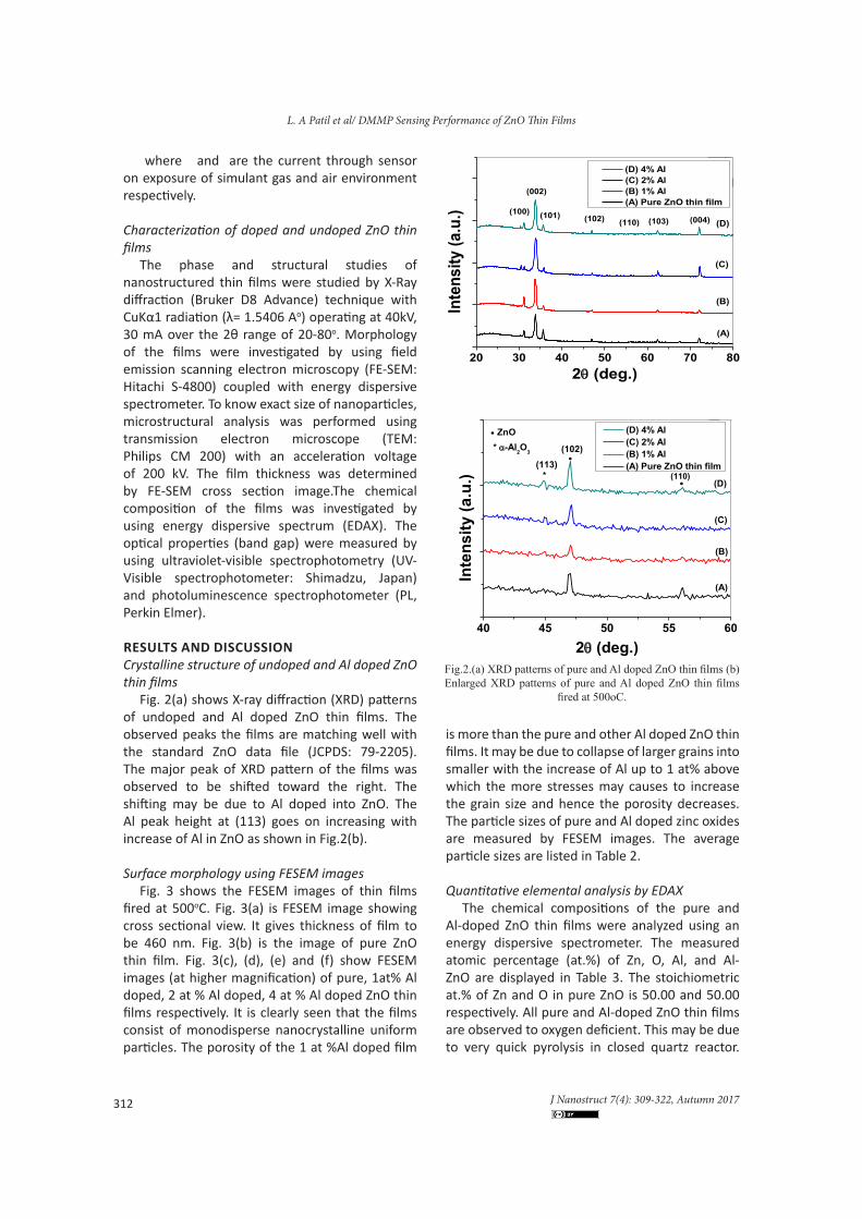
Fig. 2(a) shows X-ray diffraction (XRD) patterns of undoped and Al doped ZnO thin films. The observed peaks the films are matching well with the standard ZnO data file (JCPDS: 79-2205). The major peak of XRD pattern of the films was observed to be shifted toward the right. The shifting may be due to Al doped into ZnO. The Al peak height at (113) goes on increasing with increase of Al in ZnO as shown in Fig.2(b).
Surface morphology using FESEM imagesFig. 3 shows the FESEM images of thin films
fired at 500oC. Fig. 3(a) is FESEM image showing cross sectional view. It gives thickness of film to be 460 nm. Fig. 3(b) is the image of pure ZnO thin film. Fig. 3(c), (d), (e) and (f) show FESEM images (at higher magnification) of pure, 1at% Al doped, 2 at % Al doped, 4 at % Al doped ZnO thin films respectively. It is clearly seen that the films consist of monodisperse nanocrystalline uniform particles. The porosity of the 1 at %Al doped film
is more than the pure and other Al doped ZnO thin films. It may be due to collapse of larger grains into smaller with the increase of Al up to 1 at% above which the more stresses may causes to increase the grain size and hence the porosity decreases. The particle sizes of pure and Al doped zinc oxides are measured by FESEM images. The average particle sizes are listed in Table 2.
Quantitative elemental analysis by EDAXThe chemical compositions of the pure and
Al-doped ZnO thin films were analyzed using an energy dispersive spectrometer. The measured atomic percentage (at.%) of Zn, O, Al, and Al-ZnO are displayed in Table 3. The stoichiometric at.% of Zn and O in pure ZnO is 50.00 and 50.00 respectively. All pure and Al-doped ZnO thin films are observed to oxygen deficient. This may be due to very quick pyrolysis in closed quartz reactor.
20 30 40 50 60 70 80
Inte
nsity
(a.u
.)
2 (deg.)
(D) 4% Al (C) 2% Al (B) 1% Al (A) Pure ZnO thin film
(100)
(002)
(101) (102) (110) (103) (004)
(A)
(B)
(C)
(D)
40 45 50 55 60
Inte
nsity
(a.u
.)
2 (deg.)
(D) 4% Al (C) 2% Al (B) 1% Al (A) Pure ZnO thin film
*
(113)(102)
(110)
(A)
(B)
(C)
(D)
ZnO* -Al2O3
Fig.2.(a) XRD patterns of pure and Al doped ZnO thin films (b)Enlarged XRD patterns of pure and Al doped ZnO thin films
fired at 500oC.

313J Nanostruct 7(4): 309-322, Autumn 2017
L. A Patil et al/ DMMP Sensing Performance of ZnO Thin Films
The fine mist may not get sufficient time to gets completely oxidize. The Al-doped ZnO thin films were observed to more oxygen deficient than pure ZnO thin film. It is from EDAX results that atomic percentage (at.%) of Al goes on increasing while at.% of oxygen goes on decreasing with the increase of Al in ZnO host material.
Microstructure using TEMTEM images were carried out to know exact grain
size and microstructure. Figs. 4(a)-(c) are TEM images of 1 at.% Al doped ZnO thin film. From TEM images, it is seen that the particles are uniform in size. The selected-area electron diffraction (SAED) pattern of sample (Fig. 4d) shows nanocrystalline structure of the film.
Fig. 3. FESEM images of: undoped (a-c), 1 at %Al (d), 2 at %Al (e) and 4 at % Al (f) doped ZnO thin filmsTable 3 Chemical composition of pure and Al-doped ZnO thin films
Sr.No FESEM Images Type of Film Particle size (nm)
1 Figs. 3 (a),(b),(c) Pure ZnO 15.1
2 Fig. 3 (d) 1 at % Al ZnO 15.4
3 Fig. 3 (e) 2 at % Al ZnO 20.3
4 Fig. 3 (f) 4 at % Al ZnO 22.7
Table 2. Average particle size of pure and Al-doped zinc oxide

314
L. A Patil et al/ DMMP Sensing Performance of ZnO Thin Films
J Nanostruct 7(4): 309-322, Autumn 2017
UV-Visible spectroscopyOptical absorption spectra of pure and Al
doped ZnO films annealed at 500oC in air for 1 h are depicted in Fig. 5. The edge of absorbance is observed in the region of 330-370 nm for all the films. The absorption edge is observed to be shifted longer wavelength side with the increase of Al doping concentration. The band gap energy values observed to be decreasing with the increase of Al doping concentration are presented in Table 4.
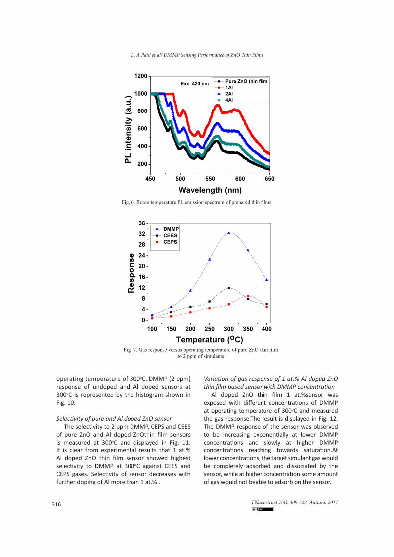
Photoluminescence spectroscopyTo measure the surface defects of the thin films,
room temperature photoluminescence (PL) spectra were carried outas shown in Fig. 6. There is broad emission spectrum in the visible range, which is caused by the structural defects [45, 46], such as interstitial of metals and oxygen vacancies. It is seen
from that PL spectrum, that the emission intensity increases with in ZnO up to 1 at.% Al. Further increase the amount of Al decay the emission intensity of thin films. Generally, stronger visible emission indicates more surface defects and thus higher gas response. It has been suggested that gas response can be remarkably enhanced with the increase of surface defects, especially electron donor ones, because much more oxygen ions can be chemisorbed and ionized on the surface of metal oxide semiconductors [47-49]. The nanoparticles with large surface-to-volume ratios have a lot of defects on the surface, which can adsorb the O2− and O− ions to form the O2−/ O− surface system. Schoenmakers et al. [50] have demonstrated that this O2−/O− surface system is the predominant trapper of the holes in the valence band, which play a key role in the formation of the visible emission centers.
Fig. 4. TEM images (a-c) and SAED image (d) of 1 at.% Al ZnO thin film.
Elements Atomic %
Pure ZnO 1 at.% Al ZnO 2 at.% Al ZnO 4 at.% Al ZnO
Zn 52.31 52.56 52.89 52.97
O 47.69 46.48 45.24 43.12
Al 0 0.96 1.87 3.91
Al-ZnO 100 100 100 100
Table 3. Chemical composition of pure and Al-doped ZnO thin films

315J Nanostruct 7(4): 309-322, Autumn 2017
L. A Patil et al/ DMMP Sensing Performance of ZnO Thin Films
Gas sensing performance of undoped and Al doped ZnOthin film based sensors
Sensing performance of the undoped and Al doped nanostructured ZnO thin film was studied by exposing them with DMMP, CEES and CEPS- the simulants of chemical warfares.
Undoped ZnO thin film based sensorsSensing performance of Undoped ZnO
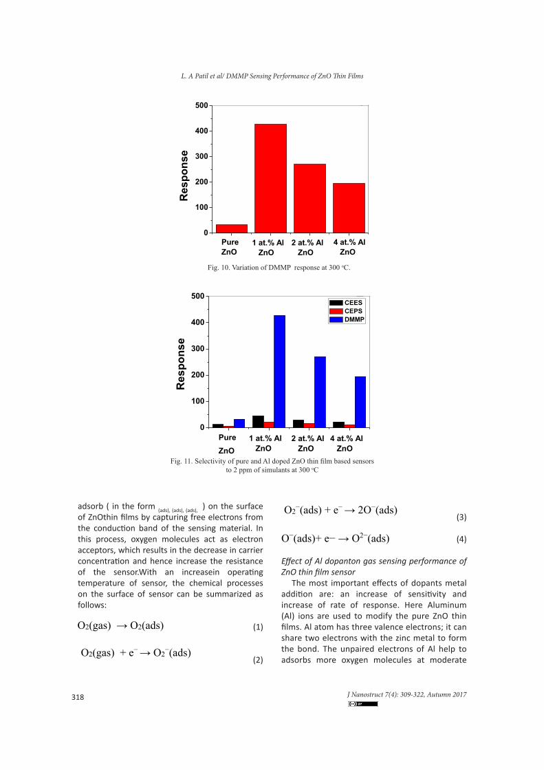
The gas sensing performance of undoped nanostructured ZnO film was investigated by exposing 2 ppm of DMMP, CEES and CEPS each separately at particular operating temperatures and gas responses of the sensor were measured. Similarly the variation of gas response of sensor with operating temperature was measured. It is clear from Fig. 7 that undoped ZnO thin film gives highest response (32.4) to DMMP at optimum operating temperature of 300oC as compared to the responses to CEES and CEPS simulants.
Selectivity of pure ZnO sensorSelectivity is important parameter of the sensor.
Selectivity of sensor is defined as the ability to selective response to particular gas in presence of other gases. Selectivity of pure ZnO thin film to DMMP against CEES and CEPS is measured at
300oC (Fig. 8). The ZnO thin film sensor showed good selectivity to DMMP as compared to CEES and CEPS gases.
Sensing performance of Al-doped ZnO thin filmsThere are two general methods to improve the
gas response of the sensor; one is by reducing the particle size of the sensor material and the other is addition of activators or dopants in the host material of sensor. Here we have adopted both methods. As prepared films are nanostructured and Al metal was used as dopants to improve the gas response of the ZnO based thin film sensor.
Gas response of Aldoped ZnO sensorThe gas response of Al doped ZnO thin film
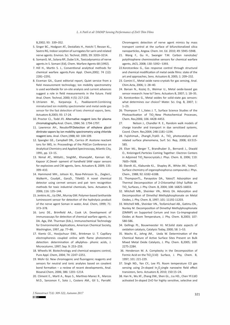
based sensors was measured by exposing 2 ppm of DMMP, CEES and CEPS each separately at different operating temperatures. Each sensor showed relatively higher response to DMMP as compared to CEES and CEPS simulants. Therefore, DMMP (2 ppm) sensing performance of each sensor was tested. Fig. 9 shows DMMP responses of different Al doped sensors at various operating temperatures. The sensor fabricated from 1 at.% Al doped ZnO thin film showed highest DMMP response (427) at an
200 300 400 500 600 700 8000.4
0.6
0.8
1.0
1.2
1.4
1.6
Abs
. (a.
u.)
Wavelength (nm)
Pure ZnO thin film 1Al 2Al 4Al
Fig. 5. Optical absorbance spectra of pure and Al doped ZnO films fired at 500 °C.
Sr.No Type of Film Spectrum Colour Band Gap Energy eV
1 Pure ZnO Black 3.06
2 1 at % Al ZnO Red 2.81
3 2 at % Al ZnO Blue 2.75
4 4 at % Al ZnO Green 2.70
Table 4. The band gap energy values calculated from absorbance spectra
316
L. A Patil et al/ DMMP Sensing Performance of ZnO Thin Films
J Nanostruct 7(4): 309-322, Autumn 2017
operating temperature of 300oC. DMMP (2 ppm) response of undoped and Al doped sensors at 300oC is represented by the histogram shown in Fig. 10.
Selectivity of pure and Al doped ZnO sensorThe selectivity to 2 ppm DMMP, CEPS and CEES
of pure ZnO and Al doped ZnOthin film sensors is measured at 300oC and displayed in Fig. 11. It is clear from experimental results that 1 at.% Al doped ZnO thin film sensor showed highest selectivity to DMMP at 300oC against CEES and CEPS gases. Selectivity of sensor decreases with further doping of Al more than 1 at.% .
Variation of gas response of 1 at.% Al doped ZnO thin film based sensor with DMMP concentration
Al doped ZnO thin film 1 at.%sensor was exposed with different concentrations of DMMP at operating temperature of 300oC and measured the gas response.The result is displayed in Fig. 12. The DMMP response of the sensor was observed to be increasing exponentially at lower DMMP concentrations and slowly at higher DMMP concentrations reaching towards saturation.At lower concentrations, the target simulant gas would be completely adsorbed and dissociated by the sensor, while at higher concentration some amount of gas would not beable to adsorb on the sensor.
450 500 550 600 650
200
400
600
800
1000
1200
PL in
tens
ity (a
.u.)
Wavelength (nm)
Pure ZnO thin film 1Al 2Al 4Al
Exc. 420 nm
Fig. 6. Room temperature PL emission spectrum of prepared thin films.
100 150 200 250 300 350 400048
12162024283236
Res
pons
e
Temperature (oC)
DMMP CEES CEPS
Fig. 7. Gas response versus operating temperature of pure ZnO thin film to 2 ppm of simulants

317J Nanostruct 7(4): 309-322, Autumn 2017
L. A Patil et al/ DMMP Sensing Performance of ZnO Thin Films
Response-recovery of the sensorThe gas response-recovery time of sensor is
also an important parameter from the practical point of view. Response time is defined as the time required to the sensor to reach 90 % of its maximum response and recovery time is the time required to get back to sensor response to 90 % of its initial state. Fig. 13 shows the 4 cycles of response-recovery curve of 1 at.% Al ZnO thin film sensor exposed to 2 ppm of DMMP at operating temperature of 300oC. The measured response and recovery time of the sensor was found to be 11 sec and 27 sec respectively. The fast response-recovery time of the sensor may be due to large surface to volume ratio of nanoparticles associated with the sensor. The nanoparticle’s surfaces are highly active to give and receive electron while
reaction take place on the surface.In present investigation, the gas response
enhancement of sensor was attempted by combining the effect of following important properties of the ZnO films: (i) its nanocrystalline nature, (ii) porous nature of thin films, and (c) activators (Al) incorporation. In recent years, ZnO and doped ZnO films have been widely used in various fields [51-53].
Oxygen adsorption on surfaces of pure and Al doped ZnOthin films
Semiconductor Metal Oxide based gas sensors give response to the gases due to change in its resistance by surface interactions [54-56]. When the sensor is exposed to air atmosphere at moderate temperatures, oxygen molecules
DMMP CEES CEPS0
5
10
15
20
25
30
35
Res
pons
e
Simulant gases (2 ppm)Fig. 8. Selectivity of pure ZnO thin film at 300 oC
100 150 200 250 300 350 400
0
100
200
300
400
500
Res
pons
e
Temperature (oC)
Pure ZnO 1 at.% Al 2 at.% Al 4 at.% Al
Fig. 9.Gas response of sensors to 2 ppm DMMP at various temperatures
318
L. A Patil et al/ DMMP Sensing Performance of ZnO Thin Films
J Nanostruct 7(4): 309-322, Autumn 2017
adsorb ( in the form (ads), (ads), (ads), ) on the surface of ZnOthin films by capturing free electrons from the conduction band of the sensing material. In this process, oxygen molecules act as electron acceptors, which results in the decrease in carrier concentration and hence increase the resistance of the sensor.With an increasein operating temperature of sensor, the chemical processes on the surface of sensor can be summarized as follows:
O2(gas) → O2(ads)
(1)
O2(gas) + e− → O2−(ads)
(2)
O2−(ads) + e− → 2O−(ads)
(3)
O−(ads)+ e− → O2−(ads)
(4)
Effect of Al dopanton gas sensing performance of ZnO thin film sensor
The most important effects of dopants metal addition are: an increase of sensitivity and increase of rate of response. Here Aluminum (Al) ions are used to modify the pure ZnO thin films. Al atom has three valence electrons; it can share two electrons with the zinc metal to form the bond. The unpaired electrons of Al help to adsorbs more oxygen molecules at moderate
0
100
200
300
400
500
4 at.% Al ZnO
2 at.% Al ZnO
Res
pons
e
Pure ZnO
1 at.% Al ZnO
Fig. 10. Variation of DMMP response at 300 oC.
0
100
200
300
400
500
4 at.% Al ZnO
2 at.% Al ZnO
Res
pons
e
CEES CEPS DMMP
PureZnO
1 at.% Al ZnO
Fig. 11. Selectivity of pure and Al doped ZnO thin film based sensors to 2 ppm of simulants at 300 oC

319J Nanostruct 7(4): 309-322, Autumn 2017
L. A Patil et al/ DMMP Sensing Performance of ZnO Thin Films
temperature on the surface of the sensor. It is seen that anoptimum amount of doping of Al(1 at.%) in ZnOenhances DMMP response. Optimum amount of Al in host would produce less crystallization of ZnO thin films (One can confirm this effect from XRD spectrum of prepared films.). Al doped ZnO thin films are found to be oxygen deficient by EDAX measurement. Hence the more oxygen molecules would be ionized and adsorbed on surface of sensor. Larger the oxygen ions adsorbed, faster would be dissociation of DMMP on Al doped films than undoped ZnO.DMMP would be adsorbed and then dissociated into MMP and MP on aluminum ions. These
fragments would then react with surface adsorbed oxygen ions and volatile components like CO2, H3PO4 and H2O would be produced.The Al doping would increase the capacity of ZnO base material to adsorb and dissociate the exposed gas-DMMP.
Gas sensing mechanism of DMMP: adsorption, dissociation and oxidation
In first step, the DMMP would be adsorbed on the surface of ZnO thin film through OP bonds and dissociated into MMP. In second step, MMP would be oxidized and converted to MP. The reaction mechanism is shown in following equations:
0 5 10 15 20 40 60 80 1000
100200300400500600700800900
Res
pons
e
DMMP conc. (ppm)Fig. 12. Variation of DMMP Response with concentration at 300 oC.
0 25 50 75 100 125 150 175 200 225
0
500
1000
1500
2000
2500
3000
OFFOFFOFF
GasON
GasON
GasON
Res
ista
nce
(k
)
Time (sec)
GasON
OFF
Fig. 13. Response-recovery of the sensor (1 at.% Al ZnO) tested at 300 oC to 2 ppm DMMP.

320
L. A Patil et al/ DMMP Sensing Performance of ZnO Thin Films
J Nanostruct 7(4): 309-322, Autumn 2017
[CH3PO(OCH3)2]ads + O−ads→ [(CH3PO2)(OCH3)]ads + (H3CO)¯ads
DMMP MMP Methoxy
[CH3PO(OCH3)2]ads + O−ads→ [(CH3PO2)(OCH3)]ads + (H3CO)¯ads
DMMP MMP Methoxy
(5)
[(CH3PO2)(OCH3)]ads+ O−ads→ [(CH3PO3)]ads+(H3CO)−ads
MMP MP Methoxy
[(CH3PO2)(OCH3)]ads+ O−ads→ [(CH3PO3)]ads+(H3CO)−ads
MMP MP Methoxy
(6)
[(CH3PO3)] ads+2(H3CO) − ads+8O−ads→3CO2+3H2O+H3PO4+8e−
MP Methoxy
[(CH3PO3)] ads+2(H3CO) − ads+8O−ads→3CO2+3H2O+H3PO4+8e−
MP Methoxy
(7)
The above reactions could be summarized as:
[(CH3PO (CH3O)2)]ads +10O− ads→H3PO4+3CO2+3H2O+10e−
[(CH3PO (CH3O)2)]ads +10O− ads→H3PO4+3CO2+3H2O+10e− (8)
The DMMP first reacts with the sensor surface through the phosphoryl oxygen, which are electron rich and can act as a Lewis base. DMMP can interact with Lewis acid sites of Zn2+, Al3+, Al2+. This results into adsorption of DMMP through PO bonds on the surface of sensor. Once DMMP is adsorbed on surface of sensor, it gets dissociated by the catalytic degradation. The dissociated DMMP diffused towards the base material where they are oxidized by adsorbed oxygen species (O -, O2
-, O2-)and finally converted into the volatile parts. It is showed [57] that DMMP (C3H9O3P) decomposes on surface of semiconducting metal oxide surface in two steps: DMMP–MMP–MP, where MMP = methyl methylphosphonate (CH3P(O2)(OCH3)) and MP= methylphosphonate (CH3PO3) with CH3O emitted at each decomposition step. In first step, DMMP would be adsorbed on ZnO surface, partially oxidized by the pre-adsorbed oxygen species and converted into residual gases.By this
process electrons get back to the conduction band of the ZnO nanoparticles and hence the resistance of the sensor decreases. In case of Al doped ZnO nanoparticles the Al particles play an important role of catalyst to adsorbed more oxygen species. These Al dopants can act as preferential adsorption sites for DMMP molecules. Also addition of Al produces more defects on the surface of the ZnO nanospheres, which can be seen from PL emission (Fig. 6). Defects enhance the gas response of the sensor.
CONCLUSIONSUndoped and Al doped nanocrystalline ZnO thin
films were successfully prepared by an ultrasonic atomization and pyrolysis method. The films consist of monodisperse particles having average particle size of 15 nm. The Al doping enhances the gas response of the ZnO sensor. The sensors exhibited high response values, fast response-recovery and good selectivity to DMMP simulant. The high DMMP response of Al doped thin films may be due to surface defects, high capability to adsorb oxygen speciesand due to presence of Al as activator and nanocrystalline nature of ZnO – the host material. Al doped (1%) ZnO thin films based sensors are observed to be promising for detection of DMMP.
ACKNOWLEDGEMENTSThe authors are thankful to the Head,
Department of Physics and Principal, Pratap College, Amalner for providing laboratory facilities for this work.
CONFLICT OF INTERESTThe author declares that there is no conflict
of interests regarding the publication of this manuscript.
REFERENCES1. Tomchenko AA., Harmer GP., Marquis BT. Detection of
chemical warfare agents using nanostructured metal oxide sensors. Sens. Actuators B, 2005; 108: 41–55.
2. Olguina C, Laguarda-Miro N, Pascual L, Garcia-Breijo E, Martinez-Manez R, Soto J., An electronic nose for the detection of Sarin, Soman and Tabun mimics and interfering agents. Sens. Actuators B,2014; 202: 31– 37.
3. Wagner GW., Bartram BW. Reactions of VX, HD and their simulants with NaY and AgY zeolites: desulfurization of VX on AgY. Langmuir,1999; 15: 8113–8118.
4. Raber E., McGuire R. Oxidative decontamination of chemical and biological warfare agents using L-Gel. J.Hazard.Mater.
321J Nanostruct 7(4): 309-322, Autumn 2017
L. A Patil et al/ DMMP Sensing Performance of ZnO Thin Films
B,2002; 93: 339–352. 5. Singer BC., Hodgson AT., Destallats H., Hotchi T, Revzan KL.,
Sextro RG, Indoor sorption of surrogates for sarin and related nerve agents. Environ. Sci. Technol, 2005; 39: 3203–3214.
6. SomaniS. M., Solana RP., Dube S.N., Toxicodynamics of nerve agents.In S. Somani (Ed), Chem. Warfare Agents 68 (1992).
7. Hill H., Martin S. J., Conventional analytical methods for chemical warfare agents.Pure Appl. Chem,2002; 74 (12): 2281–2291.
8. Eiceman GA., Guest editorial report, Quiet service from a field measurement technology; Ion mobility spectrometry is used worldwide for on-site analysis and current advances suggest a role in field measurements in the future. Field Anal. Chem. Technol, 2000; 4 (5): 217-218.
9. Utrianen M., Karpanoja E., PaakkanenH.Combining miniaturized ion mobility spectrometer and metal oxide gas sensor for the fast detection of toxic chemical vapors, Sens. Actuators B,2003; 93: 17-24.
10. Proctor CJ., Todd JFJ. Alternative reagent ions for plasma chromatography.Anal. Chem, 1984; 56: 1794-1797.
11. Lawrence AH., NeudorflP.Detection of ethylene glycol dinitrate vapors by ion mobility spectrometry using chloride reagent ions. Anal. Chem,1988; 60: 104-109.
12. Spangler GE., Campbell DN., Carrico JP. Acetone reactant ions for IMS, in: Proceedings of the PittCon Conference on Analytical Chemistry and Applied Spectroscopy, Atlantic City, 1991, pp. 13–15.
13. Nimal AT., MittalU., SinghM., KhanejaM., Kannan GK., Kapoor JC.Devel- opment of handheld SAW vapor sensors for explosives and CW agents, Sens. Actuators B, 2009; 135: 399–410.
14. Hammond MH., Johson KJ., Rose-Pehrsson SL., ZieglerJ., WalkerH., CoudyK., GaryD., TillettD. A novel chemical detector using cermet sensors and pat- tern recognition methods for toxic industrial chemicals, Sens. Actuators B, 2006; 116: 135–144.
15. Jenkins AL., Uy OM., Murray GM. Polymer-based lanthanide luminescent sensor for detection of the hydrolysis product of the nerve agent Soman in water, Anal. Chem, 1999; 71: 373–378.
16. Lenz DE., Brimfield AA., Cook LA. Development of immunoassays for detection of chemical warfare agents, in: DA. Aga, EM. Thurman (Eds.), Immunochemical Technology for Environmental Applications, American Chemical Society, Washington, 1997, pp. 77–86.
17. Kientz CE., Hooijschuur EWJ., Brinkman U. T. Capillary electrophoresis coupled online with flame photometric detection: determination of alkylphos- phonic acids, J. Microcolumn, 1997; Sep. 9: 253–259.
18. Wheelis M. Biotechnology and chemical weapons control, Pure Appl. Chem, 2004; 74: 2247–2251.
19. Mohr GJ. New chromogenic and fluorogenic reagents and sensors for neutral and ionic analytes based on covalent bond formation – a review of recent developments, Anal.Bioanal.Chem, 2006; 386: 1201–1214.
20. Climent E., Marti A., Royo S., Martínez-Manez R., Marcos M.D., Sancenon F., Soto J., Costero AM., Gil S., ParraM.
Chromogenic detection of nerve agent mimics by mass transport control at the surface of bifunctionalized silica nanoparticles, Angew. Chem. Int. Ed. 2010; 49: 5945–5948.
21. Wang F., Gu H., Swanger T.M. Carbon nanotube/polythiophene chemiresistive sensors for chemical warfare agents, JACS, 2008; 130: 5392– 5393.
22.Korotcenkov G., Gas response control through structural and chemical modification of metal oxide films: state of the art and approaches, Sens. Actuators B, 2005; 1: 209–232.
23. Comini E., Metal oxide nano-crystals for gas sensing, Anal. Chim.Acta, 2006; 1: 28–40.
24. Barsan N., Koziej D., Weimar U., Metal oxide-based gas sensor research: how to? Sens. Actuators B, 2007; 1: 18–35.
25. Korotcenkov G., Metal oxides for solid-state gas sensors: what determines our choice? Mater. Sci. Eng. B, 2007; 1: 1–23.
26. Thompson T. L.,Yates J. T., Surface Science Studies of the Photoactivation of TiO2-New Photochemical Processes, Chem. Rev,2006; 106: 4428–4453.
27. Nelson J., Chandler R. E., Random walk models of charge transfer and transport in dye sensitized systems, Coord. Chem. Rev,2004; 248:1181–1194.
28. FujishimaA., ZhangX.,TrykD. A., TiO2 photocatalysis and related surface phenomena, Surf. Sci. Rep, 2008; 63:515-585.
29. Elser MJ., Berger T., Brandhuber D., Bernardi J., Diwald O., KnözingerE.Particles Coming Together: Electron Centers in Adjoined TiO2 Nanocrystals.J. Phys. Chem. B, 2006; 110: 7605–7608.
30. Ekerdt JG., Klabunde KJ., Shapley JR., White JM., YatesJT.Surface chemistry of organophosphorus compounds.J. Phys. Chem., 1988; 92: 6182–6188.
31. ThompsonTL., Panayotov DA., YatesJT. Adsorption and Thermal Decomposition of 2-Chloroethyl Ethyl Sulfide on TiO2 Surfaces, J. Phy. Chem. B, 2004; 108: 16825-16833.
32. Mitchell MB., Sheinker VN., Mintz EA. Adsorption and Decomposition of Dimethyl Methylphosphonate on Metal Oxides, J. Phy. Chem. B, 1997; 101: 11192-11203.
33. Mitchell MB., Sheinker VN., Tesfamichael AB., Gatimu EN., Nunley M. Decomposition of Dimethyl Methylphosphonate (DMMP) on Supported Cerium and Iron Co-Impregnated Oxides at Room Temperature, J. Phy. Chem. B,2003; 107: 580-586.
34. Gellings PJ., Bouwmeester HJ. M.Solid state aspects of oxidation catalysis, Catalysis Today, 2000; 58: 1–53.
35. Wachs IE., Jehng JM., Ueda W. Determination of the Chemical Nature of Active Surface Sites Present on Bulk Mixed Metal Oxide Catalysts, J. Phy. Chem. B,2005; 109: 2275-2284.
36. Henderson M. A. Complexity in the Decomposition of Formic Acid on the TiO2(110) Surface, J. Phy. Chem. B, 1997; 101: 221-229.
37. Singh ND., Yan CY., Lee PS. Room temperature CO gas sensing using Zn-doped In2O3single nanowire field effect transistors, Sens. Actuators B, 2010; 150:15–24.
38. Han N., Wu XF., Zhang DW., Shen GL., Liu HD., Chen YF.CdO activated Sn-doped ZnO for highly sensitive, selective and

322
L. A Patil et al/ DMMP Sensing Performance of ZnO Thin Films
J Nanostruct 7(4): 309-322, Autumn 2017
stable formaldehyde sensor, Sens. Actuators B, 2011; 152: 324–329.
39. Song P., Wang Q., Yang ZX. Preparation, characterization and acetone sensing g properties of Ce-doped SnO2 hollow spheres, Sens. Actuators B, 2012; 173: 839–846.
40. Azmy N., Abdullah H., Naim NM., Hamid AA., ShaariS., MokhtarW.H.M.W., Gamma irradiation effect on the structural, morphology and electrical proper-ties of ZnO–CuO doped PVA nanocomposite thin films for Escherichia coli sensor, Radiat. Phys. Chem, 2014; 103: 108–113.
41. Bi L., Dong XT., Yu YH., Room-temperature phosphorescence sensor based on manganese doped zinc sulfide quantum dots for detection of urea, J. Lumin, 2014; 153: 356–360.
42. Han D, Song P, Zhang S, Zhang H, Xu Q, Wang W., Enhanced methanol gas-sensing performance of Ce-doped In2O3 porous nanospheres prepared by hydrothermal method, Sens. Actuators B, 2015; 216: 488–496.
43. Patil LA., Shinde MD., Bari AR., Deo VV.Novel trapping system for size wise sorting of SnO2 nanoparticles synthesized from pyrolysis of ultrasonically atomized spray for gas sensing, Sens. Actuators B, 2009; 143: 316–324.
44. Patil LA., Deo VV., Shinde MD., Bari AR., Kaushik MP., Sensing of 2-chloroethyl ethyl sulfide (2-CEES) – a CWA simulant – using pure and platinum doped nanostructured CdSnO3 thin films prepared from ultrasonic spray pyrolysis technique, Sens. Actuators B, 2011; 160: 234– 243.
45. McCluskey MD, Jokela SJ. “Defects in ZnO,” JApplied Physics, 2009; 106: 071101-071113.
46. Ilican S., Caglar Y., CaglarM. (Preparation and characterization of ZnO thin films
deposited by sol-gel spin coating method), J. Optoelectron. Adv. Mater., 2008; 10: 2578-2583.
47. Ahn MW., Park KS., Heo JH., Park JG., Kim DW., Choi KJ., Lee JH., Hong SH. “Gas sensing properties of defect-controlled ZnO-nanowire gas sensor,” App. Phys. Letters,
2008; 93(26): 263103-263105.48. Han N., Hu P., Zuo A., Zhang D., Tian Y., Chen Y.
“Photoluminescence investigation on the gas sensing property of ZnOnanorods prepared by plasma enhanced CVD method,” Sens. Actuators B, 2010;145(1): 114–119.
49. Zhang T., Zeng Y., Fan HT., Wang LJ., Wang R., Fu WY.,Yang HB., “Synthesis, optical and gas sensitive properties of large-scale aggregative flowerlike ZnO nanostructures via simple route hydrothermal process,” J.of Physics D: Appl.Phys, 2009; 42(4): 045103-045110.
50. Schoenmakers GH., Vanmaekelbergh D., Kelly JJ.Study of charge carrier dynamics at illuminated ZnO photoanodes, J. Phys. Chem, 1996; 100: 3215-3220.
51. Zhezhe W., Hongchao S., Rongjun Z., Xinxin X., Yude W., ZnO Nanoparticles as Sensing Materials with High Gas Response for Detection of n-butanol Gas, J Nanostruct, 2017; 7(2): 103-11.
52. Mohammad HM, Mehdi A., Mohammad S.,Preparation and Characterization of ZnO Thin Layers with Various Percentages of Gallium Impurities, JNanostruct, 2017; 7(3): 194-199.
53. Xu L, Yan Y, Yunfei H, Lihong W, Gang C, Xuechun X, Yude W, H2O2-based Green Corrosion Route to ZnOMicrorodsPhotocatalysts on Zn Plate, J Nanostruct, 2017; 7(1): 82-87.
54. Morrison S. Roy, Semiconductor gas sensors, 1982Sens. Actuators, 1982; 2: 329-341.
55. Yamazoe N., New approaches for improving semiconductor gas sensors Sens. Actuators B, 1991; 5(1-4): 7-19.
56. Egashira M., Shimizu Y., Takao Y., Sako S., Variations in I–V characteristics of oxide semiconductors induced by oxidizing gases, 1996 Sens. Actuators B, 1996; 35:62-67.
57. Kohl D. The role of noble metals in the chemistry of solid-state gas sensors, Sens. Actuators B, 1990; 1: 158–165.