Embed Size (px)
Citation preview
DMA Controller(8237 Programming Examples)
Dr A SahuDept of Comp Sc & Engg.
IIT Guwahati
Outline• 8259 Control and Operation word• 8259 programming and interrupts• Nested Interrupts • DMA controller• DMA Architecture• Introduction to Programming DMA (Next
class)• Next class will be in Room 1201
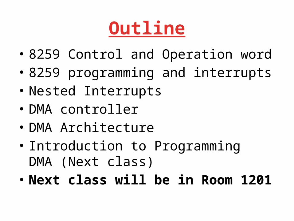
Block Diagram of 8259
8259A Programmable
Interrupt Controller
IRQ0
IRQ1
IRQ2IRQ3
IRQ4
IRQ5
IRQ6
IRQ7
8 bitData Bus
RDb
WRb
CSb
A0
INTINTAb
SPb/ENb
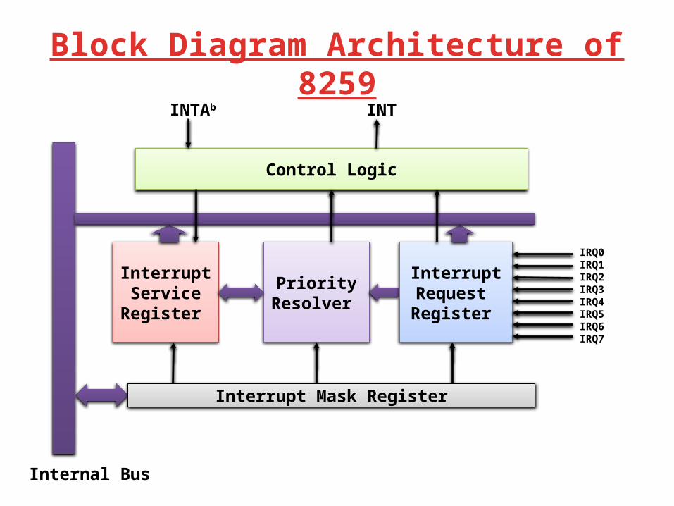
Control Logic
Interrupt Service
Register
Priority Resolver
Interrupt Request Register
IRQ0IRQ1IRQ2IRQ3IRQ4IRQ5IRQ6IRQ7
Interrupt Mask Register
Internal Bus
INTAb INT
Block Diagram Architecture of 8259
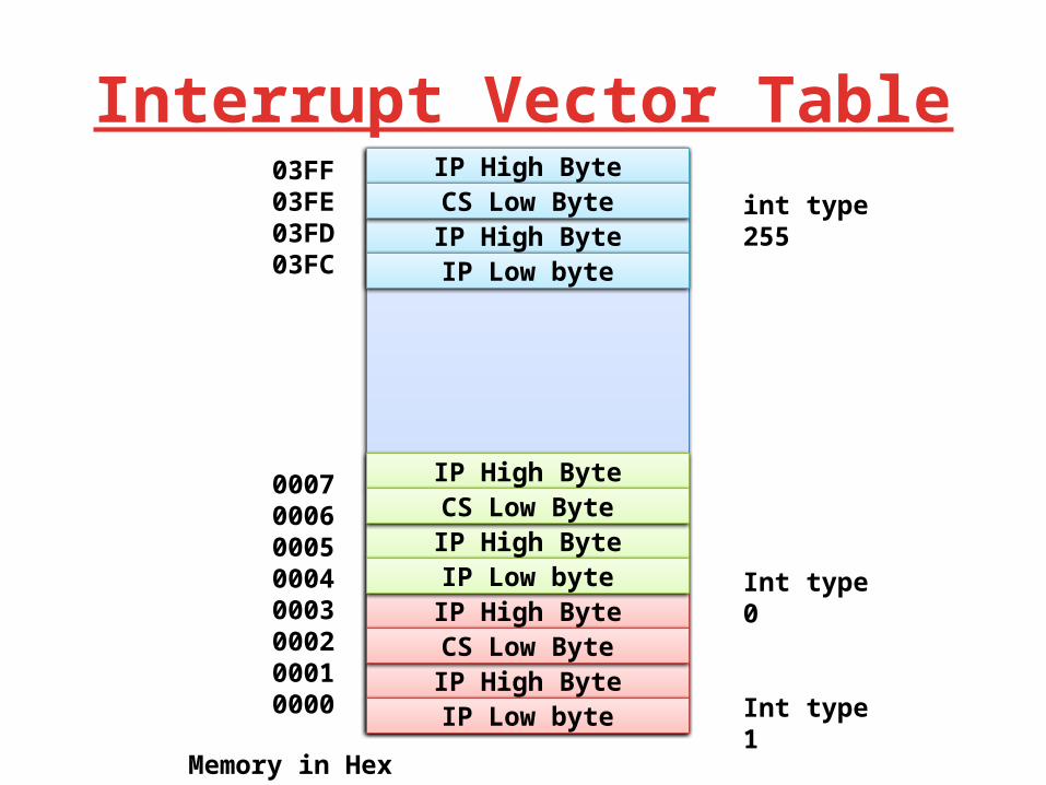
Interrupt Vector Table03FF03FE03FD03FC
00070006000500040003000200010000
int type 255
Int type 0
Int type 1
Memory in Hex
IP High ByteIP Low byte
IP High ByteCS Low Byte
IP High ByteIP Low byte
IP High ByteCS Low Byte
IP High ByteIP Low byte
IP High ByteCS Low Byte
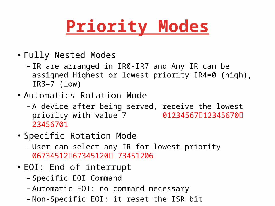
Priority Modes
• Fully Nested Modes– IR are arranged in IR0-IR7 and Any IR can be assigned Highest
or lowest priority IR4=0 (high), IR3=7 (low)• Automatics Rotation Mode– A device after being served, receive the lowest priority with
value 7 0123456712345670 23456701 • Specific Rotation Mode– User can select any IR for lowest priority
0673451267345120 73451206 • EOI: End of interrupt– Specific EOI Command– Automatic EOI: no command necessary– Non-Specific EOI: it reset the ISR bit
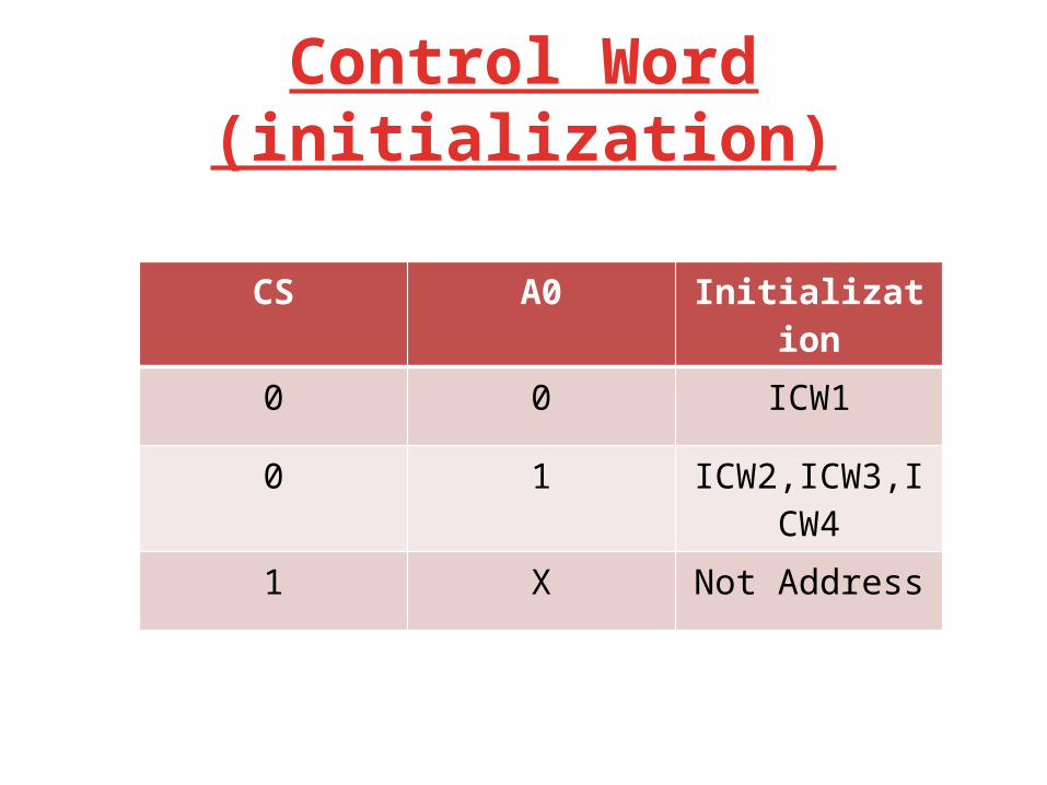
Control Word (initialization)
CS A0 Initialization
0 0 ICW1
0 1 ICW2,ICW3,ICW4
1 X Not Address
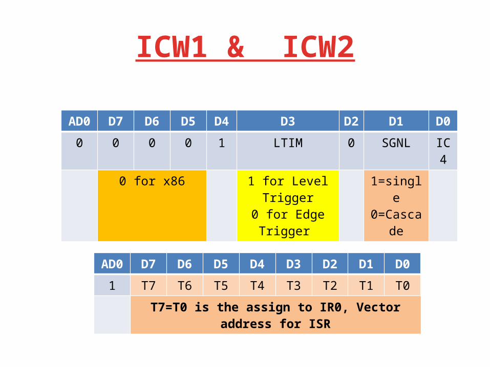
ICW1 & ICW2
AD0 D7 D6 D5 D4 D3 D2 D1 D0
0 0 0 0 1 LTIM 0 SGNL IC4
0 for x86 1 for Level Trigger0 for Edge Trigger
1=single0=Cascade
AD0 D7 D6 D5 D4 D3 D2 D1 D0
1 T7 T6 T5 T4 T3 T2 T1 T0
T7=T0 is the assign to IR0, Vector address for ISR
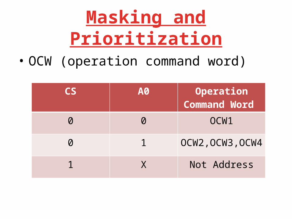
Masking and Prioritization
• OCW (operation command word)
CS A0 Operation Command Word
0 0 OCW1
0 1 OCW2,OCW3,OCW4
1 X Not Address
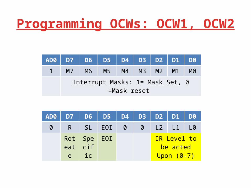
Programming OCWs: OCW1, OCW2
AD0 D7 D6 D5 D4 D3 D2 D1 D0
1 M7 M6 M5 M4 M3 M2 M1 M0
Interrupt Masks: 1= Mask Set, 0 =Mask reset
AD0 D7 D6 D5 D4 D3 D2 D1 D0
0 R SL EOI 0 0 L2 L1 L0
Roteate
Specific
EOI IR Level to be acted Upon (0-7)
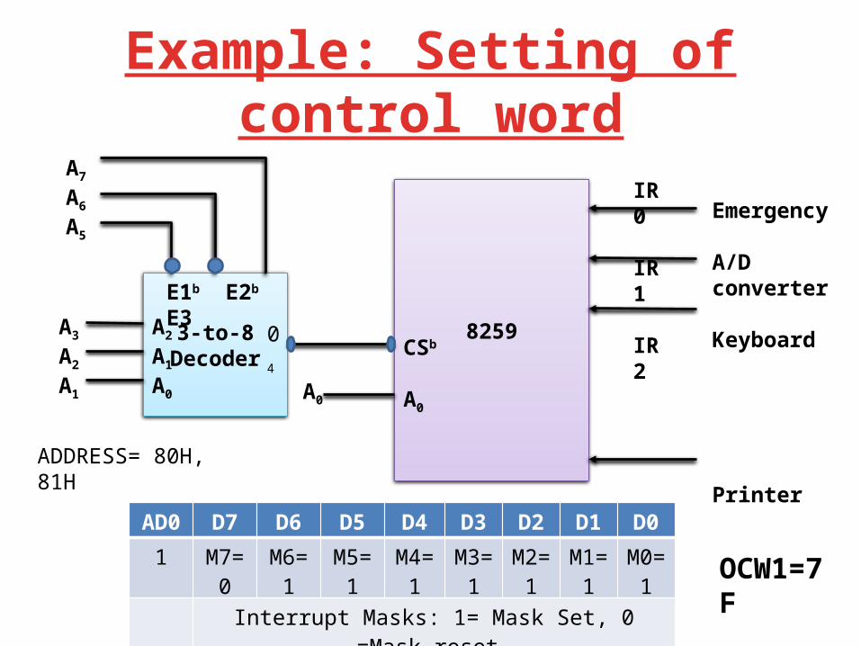
Example: Setting of control word
8259
IR0
IR1
IR2
IR6
Emergency
A/D converter
Keyboard
Printer
3-to-8Decoder CSb
A0
E1b E2b E3
A2
A1
A0
A3
A2
A1
A7
A6
A5
A0
AD0 D7 D6 D5 D4 D3 D2 D1 D0
1 M7=0
M6=1
M5=1
M4=1
M3=1
M2=1
M1=1
M0=1
Interrupt Masks: 1= Mask Set, 0 =Mask reset
OCW1=7F
ADDRESS= 80H, 81H
04
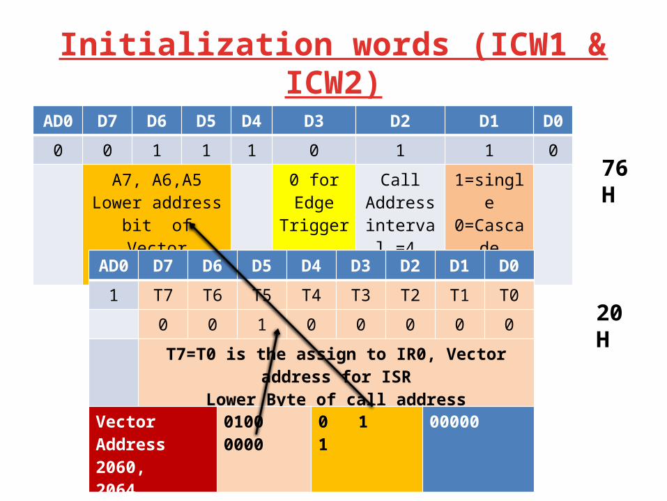
Initialization words (ICW1 & ICW2)AD0 D7 D6 D5 D4 D3 D2 D1 D0
0 0 1 1 1 0 1 1 0
A7, A6,A5Lower address bit of Vector Address
0 for Edge Trigger
Call Address
interval =4
1=single0=Cascade
AD0 D7 D6 D5 D4 D3 D2 D1 D0
1 T7 T6 T5 T4 T3 T2 T1 T0
0 0 1 0 0 0 0 0
T7=T0 is the assign to IR0, Vector address for ISRLower Byte of call address
76H
20H
Vector Address 2060, 2064….
0100 0000 0 1 1 00000
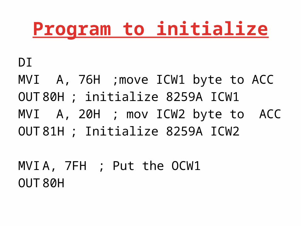
Program to initialize
DIMVI A, 76H ;move ICW1 byte to ACCOUT 80H ; initialize 8259A ICW1MVI A, 20H ; mov ICW2 byte to ACCOUT 81H ; Initialize 8259A ICW2
MVI A, 7FH ; Put the OCW1OUT 80H
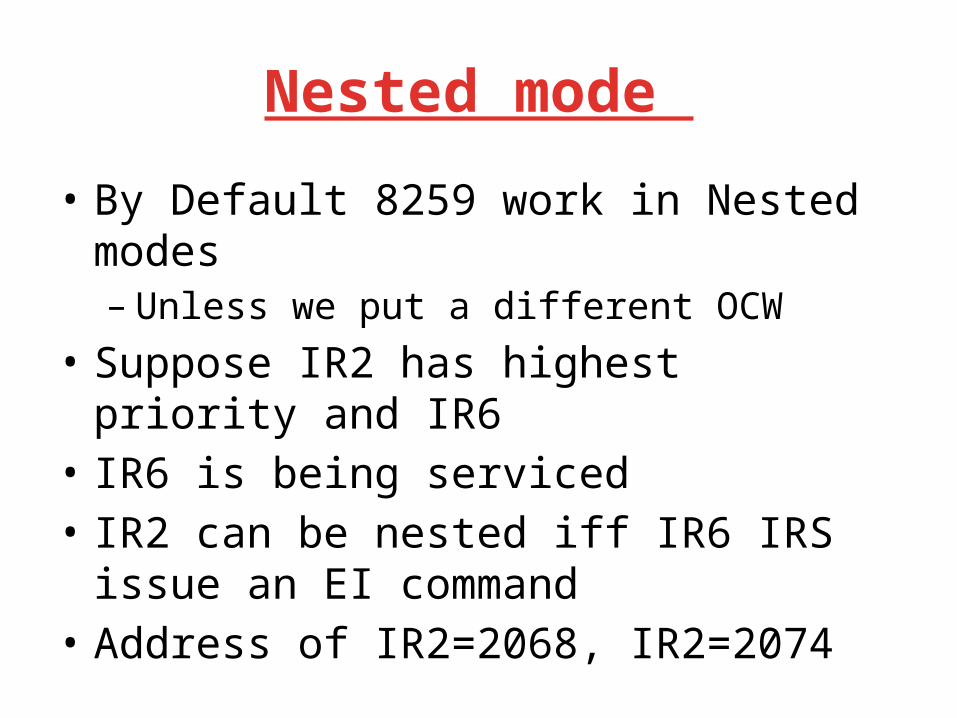
Nested mode
• By Default 8259 work in Nested modes– Unless we put a different OCW
• Suppose IR2 has highest priority and IR6• IR6 is being serviced• IR2 can be nested iff IR6 IRS issue an EI
command• Address of IR2=2068, IR2=2074
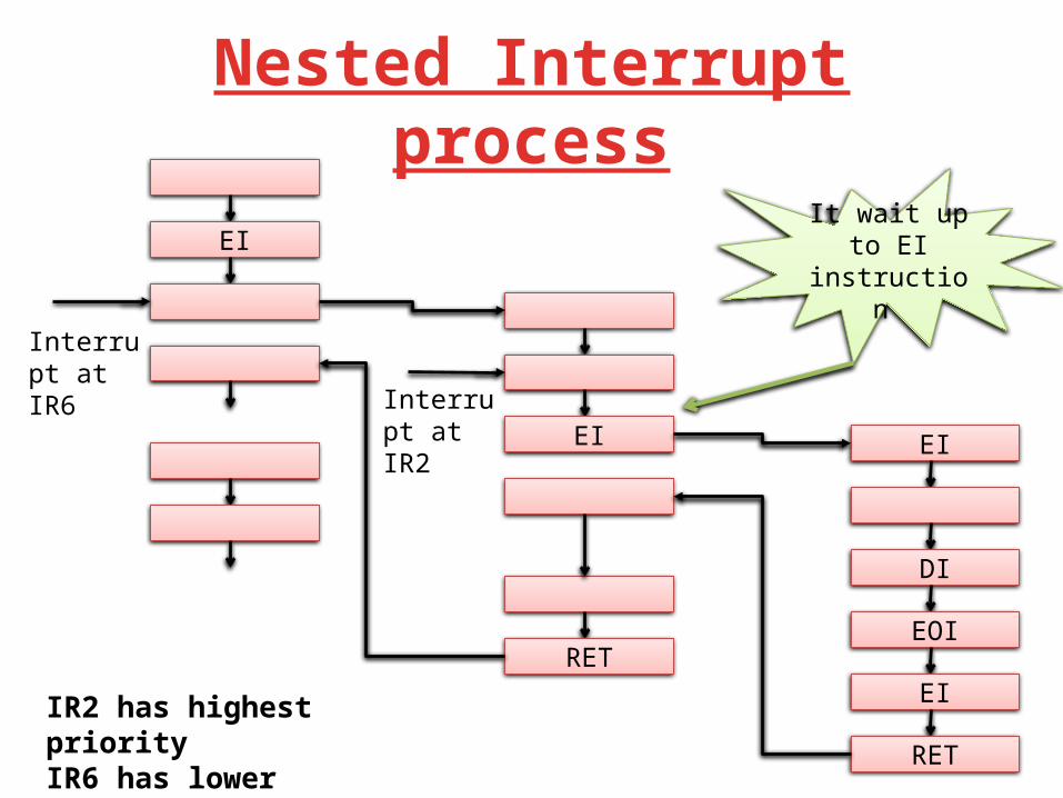
Nested Interrupt process
EI
EI
RET
EI
DI
EOI
EI
RET
Interrupt at IR6
Interrupt at IR2
It wait up to EI instruction
IR2 has highest priorityIR6 has lower priority
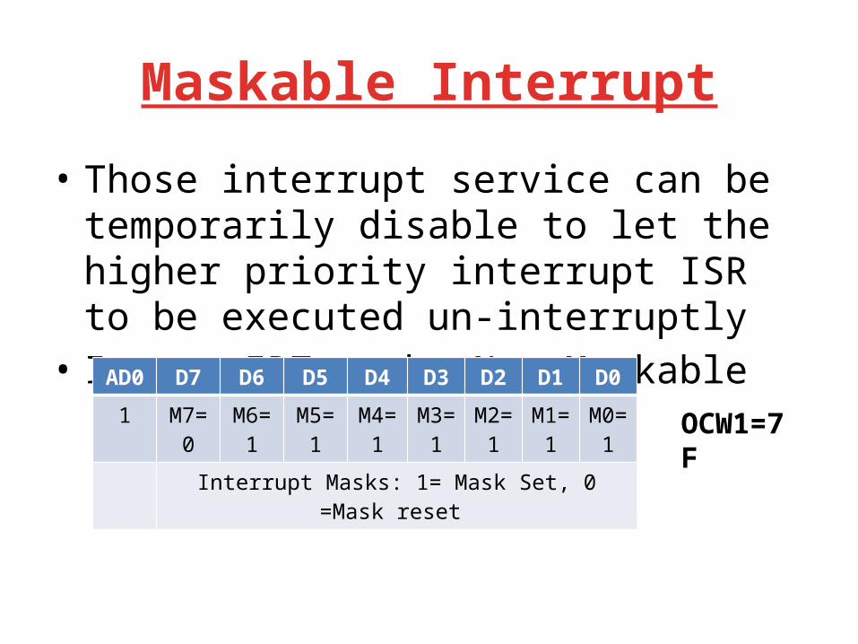
Maskable Interrupt
• Those interrupt service can be temporarily disable to let the higher priority interrupt ISR to be executed un-interruptly
• I want IR7 to be Non Maskable AD0 D7 D6 D5 D4 D3 D2 D1 D0
1 M7=0
M6=1
M5=1
M4=1
M3=1
M2=1
M1=1
M0=1
Interrupt Masks: 1= Mask Set, 0 =Mask reset OCW1=7F
DMA
• Direct memory access • DMA Controller • DMA mode of I/O• Programmed mode I/O vs DMA mode I/O
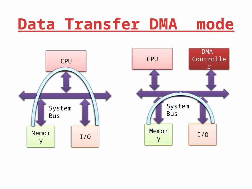
Data Transfer DMA mode
Memory
CPU DMA ControllerCPU
I/O
System Bus
Memory I/O
System Bus
Data Transfer
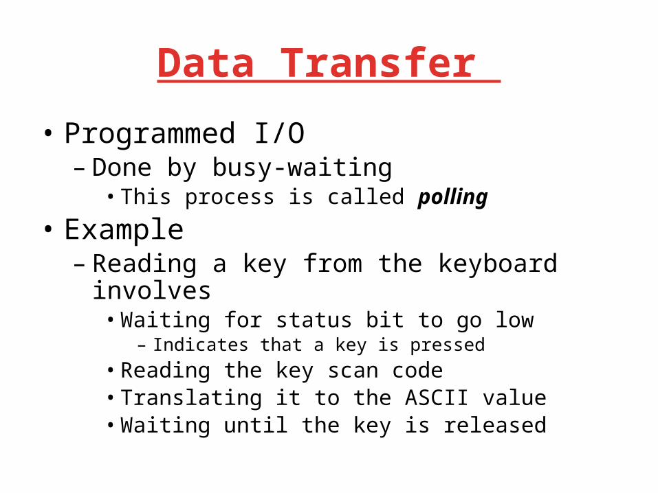
• Programmed I/O– Done by busy-waiting• This process is called polling
• Example– Reading a key from the keyboard involves• Waiting for status bit to go low
– Indicates that a key is pressed• Reading the key scan code• Translating it to the ASCII value• Waiting until the key is released
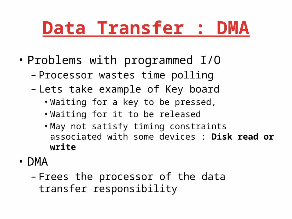
Data Transfer : DMA
• Problems with programmed I/O– Processor wastes time polling– Lets take example of Key board
• Waiting for a key to be pressed, • Waiting for it to be released• May not satisfy timing constraints associated with some
devices : Disk read or write
• DMA– Frees the processor of the data transfer
responsibility
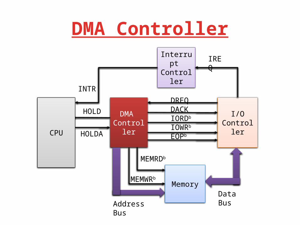
DMA Controller
Interrupt Controller
I/O Controller
DMA Controller
IREQ
DREQDACKIORDb
IOWRb
EOPb
MEMRDb
MEMWRb
INTR
HOLD
HOLDA
Data BusAddress Bus
CPU
Memory
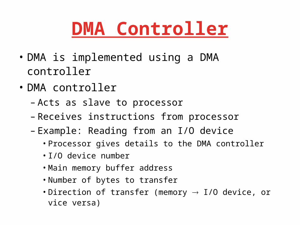
DMA Controller• DMA is implemented using a DMA controller• DMA controller– Acts as slave to processor– Receives instructions from processor– Example: Reading from an I/O device
• Processor gives details to the DMA controller• I/O device number• Main memory buffer address• Number of bytes to transfer• Direction of transfer (memory I/O device, or vice versa)
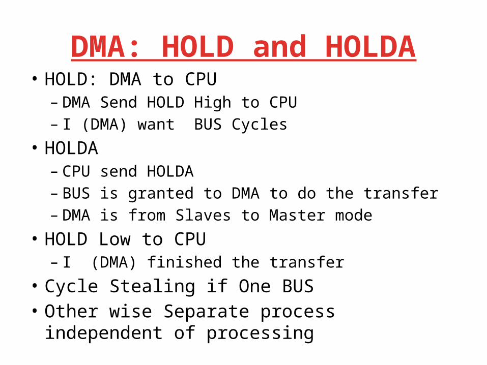
DMA: HOLD and HOLDA• HOLD: DMA to CPU– DMA Send HOLD High to CPU – I (DMA) want BUS Cycles
• HOLDA– CPU send HOLDA– BUS is granted to DMA to do the transfer– DMA is from Slaves to Master mode
• HOLD Low to CPU – I (DMA) finished the transfer
• Cycle Stealing if One BUS • Other wise Separate process independent of
processing
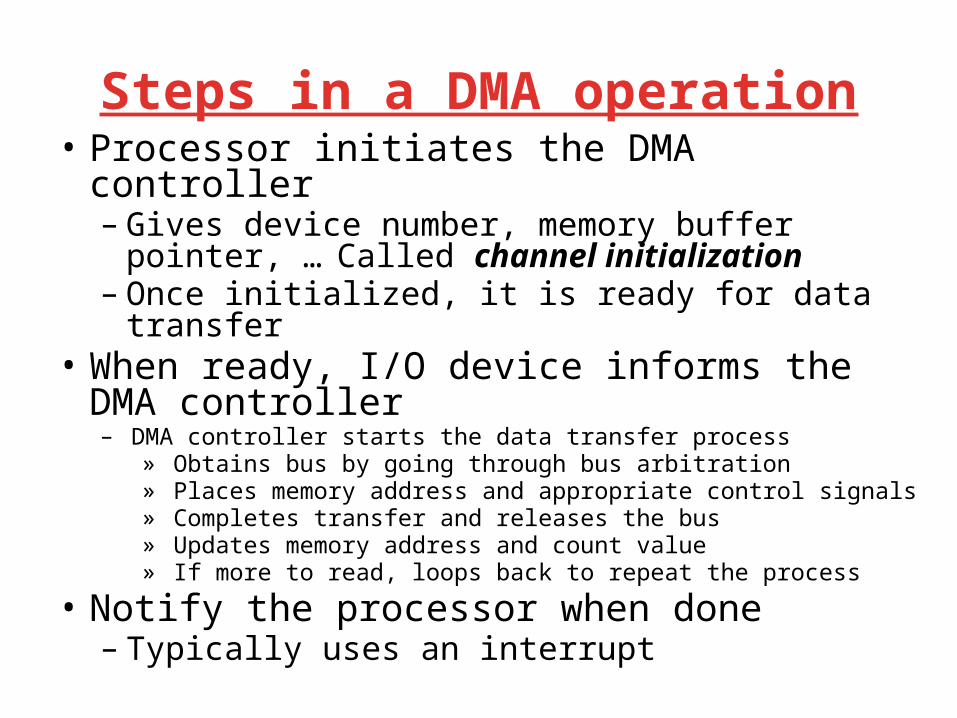
Steps in a DMA operation• Processor initiates the DMA controller – Gives device number, memory buffer pointer, …
Called channel initialization– Once initialized, it is ready for data transfer
• When ready, I/O device informs the DMA controller – DMA controller starts the data transfer process
» Obtains bus by going through bus arbitration» Places memory address and appropriate control signals» Completes transfer and releases the bus» Updates memory address and count value» If more to read, loops back to repeat the process
• Notify the processor when done– Typically uses an interrupt
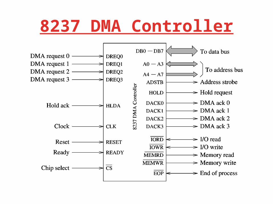
8237 DMA Controller
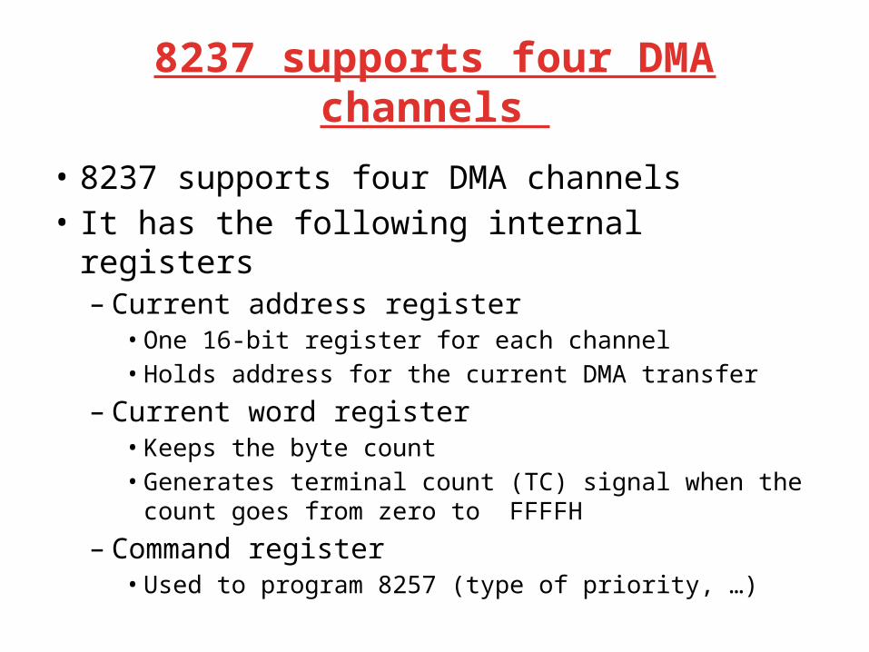
8237 supports four DMA channels
• 8237 supports four DMA channels • It has the following internal registers– Current address register
• One 16-bit register for each channel• Holds address for the current DMA transfer
– Current word register• Keeps the byte count• Generates terminal count (TC) signal when the count
goes from zero to FFFFH
– Command register• Used to program 8257 (type of priority, …)
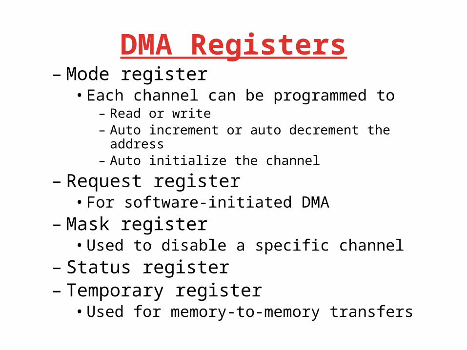
DMA Registers– Mode register• Each channel can be programmed to
– Read or write– Auto increment or auto decrement the address– Auto initialize the channel
– Request register• For software-initiated DMA
– Mask register• Used to disable a specific channel
– Status register– Temporary register• Used for memory-to-memory transfers
Type of Data Transfer using 8237 DMA• Single cycle transfer – Only single transfer takes place – Useful for slow devices
• Block transfer mode – Transfers data until TC is generated or external EOPb
signal is received• Demand transfer mode – Similar to the block transfer mode – In addition to TC and EOP, transfer can be
terminated by deactivating DREQ signal• Cascade mode– Useful to expand the number channels beyond four

Programming DMA
• Next Class…

Next class will be in Room 12017 Sept 2010 onwards
Reference
• R S Gaonkar, “Microprocessor Architecture”, Chapter 15

Thanks


![INJNTU...Draw the Inter facing diagram of 8257 DMA with 8086 CPU and explain its operation. [8M) Explain ICW's and OCW's of 8259 Priority interrupt controller. [8M] Draw the 8257 DMA](https://img.pdfslide.net/doc/110x75/5e65f7e1da78ad43396912bf/injntu-draw-the-inter-facing-diagram-of-8257-dma-with-8086-cpu-and-explain-its.jpg)