Embed Size (px)
Citation preview
HAL Id: tel-01499842https://tel.archives-ouvertes.fr/tel-01499842
Submitted on 1 Apr 2017
HAL is a multi-disciplinary open accessarchive for the deposit and dissemination of sci-entific research documents, whether they are pub-lished or not. The documents may come fromteaching and research institutions in France orabroad, or from public or private research centers.
L’archive ouverte pluridisciplinaire HAL, estdestinée au dépôt et à la diffusion de documentsscientifiques de niveau recherche, publiés ou non,émanant des établissements d’enseignement et derecherche français ou étrangers, des laboratoirespublics ou privés.
DRC et LVS pour la conception photonique sur siciliumRuping Cao
To cite this version:Ruping Cao. DRC et LVS pour la conception photonique sur sicilium. Autre. Université de Lyon,2016. Français. �NNT : 2016LYSEC009�. �tel-01499842�
N° ordre : 2016LYSEC009
Thèse de l'Université de Lyon
Délivrée par l’Ecole Centrale de Lyon Spécialité : Conception des Systèmes hétérogènes
Soutenue publiquement le 25 Mars 2016
par
Mme. Ruping Cao
Préparée à l’Institut des Nanotechnologies de Lyon (INL) (UMR5270), Mentor Graphics Ireland Ltd French Branch
DRC et LVS pour la Conception
Photonique sur Silicium
Ecole Doctorale Electronique, Electrotechnique, Automatique
Composition du jury : Prof. Eric Cassan, Université Paris-Sud, en qualité de Président Dr. Marie-Minerve Louërat, Université Paris 6, en qualité de Rapporteur Prof. Dries Van Thourhout, Ghent University, en qualité de Rapporteur Dr. Charles Baudot, STMicroelectronics, en qualité d’Examinateur Prof. Ian O’Connor, Ecole Centrale de Lyon, en qualité de Directeur Alexandre Arriordaz, Mentor Graphics, en qualité d’Encadrant
1
Abstract
Silicon with its mature integration platform has brought electronic circuits to mass-market
applications; silicon photonics will most probably follow this evolution. However, there are still
many technological challenges to be addressed in order to realize silicon photonics technology.
One of the key challenges is building a complete design environment interfaced with standard
EDA tools; as in microelectronics, this would enable the creation of photonic libraries and
photonic IP blocks. In this study, we focus on developing a physical verification (PV) flow for
the silicon photonics technology.
There are a number of components from the traditional CMOS IC physical verification world
that can be borrowed. All, however, will require some modification due to the distinct nature of
photonic circuits. We study the photonic circuit PV requirements, in comparison with those for
traditional IC designs. The most significant limitation of current PV tools is to handle non-
Manhattan layout designs. We adapt industrial standard PV tools to perform efficient and
reliable design rule checking (DRC) that validates non-Manhattan like layout. We also propose
methodologies and develop a layout versus schematic (LVS) checking flow specific to the non-
Manhattan characteristics and photonic circuit verification requirements. The flow is capable
of verifying photonic circuit layout implementation (or even manufactured silicon) with regard
to the intended design. The developed flows are demonstrated with Mentor Graphics Pyxis
design environment and Calibre® PV tool suit. As generic methodologies, they can also be in
principle adopted in other EDA tool environments in order to verify the physical
implementation of the photonic designs. Such a PV flow is essential for bringing the silicon
photonics technology onto the real CMOS streamline.
Résumé
La plate-forme d'intégration silicium est arrivée à maturité, et a amené les circuits intégrés
électroniques (IC) aux applications du marché de masse ; la photonique sur silicium va suivre
probablement cette évolution. Pourtant, il y a encore de nombreux défis technologiques à
relever pour réaliser la technologie photonique sur silicium. Parmi les principaux défis, il est
essentiel de se concentrer sur la construction d'un environnement de conception complet
interfacé avec les outils EDA standards ; comme dans la microélectronique, il permettrait la
création de librairies photoniques et des blocs IP photoniques. Dans cette étude, nous nous
concentrons sur l’adaptation et le développement du flot de vérification physique (PV, ou «
physical verification ») pour la conception photonique sur silicium.
Il y a un certain nombre de concepts de PV existant pour le CMOS traditionnel qui peuvent être
empruntés. Tous, cependant, nécessiteront quelques modifications en raison de la nature
distincte du circuit photonique. Nous étudions les exigences de PV pour les circuits photoniques,
en comparaison avec celles de la conception de circuits intégrés traditionnels. La limitation la
plus importante des outils de PV actuels est de traiter les layout « non-Manhattan ». Nous
adaptons des outils industriels standards pour effectuer un « design rule checking » (DRC)

2
efficace et fiable qui valide les layout non-Manhattan. Nous proposons également des
méthodologies et développons un flot « layout versus schematic » (LVS) spécifique aux
caractéristiques non-Manhattan et aux exigences de vérification de circuits photoniques. Le flot
est capable de vérifier le layout du circuit photonique (ou même le silicium fabriqué du circuit)
en ce qui concerne la conception cible. Les flots développés sont démontrées avec les outils de
Mentor Graphics – Pyxis (l’environnement de dessin) et Calibre® (les outils de PV). Comme
les méthodologies génériques, ils peuvent aussi être en principe adoptés dans d'autres outils
EDA afin d'effectuer la vérification de la réalisation de la conception du circuit photonique. Un
tel flot de PV est essentiel pour amener la technologie photonique sur silicium sur la ligne de
production réelle de CMOS.
3
Table of Contents
Chapter 1 INTRODUCTION & BACKGROUND .................................................................. 8
1.1 Silicon Photonics ........................................................................................................ 8
1.1.1 Bringing light to the chip ...................................................................................... 8
1.1.2 Leveraging silicon platform for integrated photonics ............................................. 12
1.1.3 Challenges ahead .............................................................................................. 15
1.2 Design Tools for PIC................................................................................................. 17
1.2.1 CAD tools for photonic designs ........................................................................... 17
1.2.2 Leveraging EDA for photonic designs .................................................................. 20
1.2.3 The EDA methodology and the PDK .................................................................... 21
1.2.4 Review of current integrated design environments ................................................. 23
1.3 The PV Methodology ................................................................................................. 29
Chapter 2 PHYSICAL VERIFICATION FOR PHOTONIC DESIGNS – REQUIREMENTS
AND LIMITATIONS ............................................................................................................. 32
2.1 Design Rule Checking ............................................................................................... 32
2.1.1 The non-Manhattan layout geometry .................................................................... 33
2.1.2 Curvilinear design in GDS format ........................................................................ 35
2.1.3 Dimensional measurement on snapped polygons ................................................... 35
2.1.4 DRC false error and missed error ........................................................................ 36
2.1.5 Handling advanced fabrication constraints ........................................................... 38
2.1.6 Density and fill insertion ..................................................................................... 39
2.2 Layout vs. Schematic Checking ................................................................................... 39
2.2.1 Curvilinear features in PICs ............................................................................... 41
2.2.2 Handling curvilinear data in standard layout format .............................................. 44
2.2.3 Representation of photonic device feature in standard netlist format ........................ 44
2.2.4 Representation of waveguide interconnect in standard netlist format........................ 45
2.2.5 Photonic device and connectivity definition ........................................................... 45
2.2.6 Device parameter comparison ............................................................................. 47
2.3 Design for Manufacturing .......................................................................................... 48
2.3.1 Process impact on photonic designs ..................................................................... 48
2.3.2 Lithographic checking ........................................................................................ 49
2.4 Considerations on Post-Layout Flow ........................................................................... 50
Chapter 3 DESIGN RULE CHECKING (DRC) .................................................................. 53
3.1 Solutions to DRC on Non-Manhattan Designs .............................................................. 53

4
3.1.1 Conditional DRC result post-filtering ................................................................... 53
3.1.2 Multi-dimensional rule check .............................................................................. 54
3.1.3 Enable measurement of non-conventional dimensions ............................................ 56
3.2 Experiments & Results .............................................................................................. 56
3.2.1 False error filtering ........................................................................................... 56
3.2.2 Multi-dimensional rule check with physical model ................................................. 59
3.2.3 Measurement on non-conventional dimensions ...................................................... 63
3.2.4 Performance test ................................................................................................ 64
3.3 Testcase Summary and Conclusions ............................................................................ 65
Chapter 4 LAYOUT VS. SCHEMATIC (LVS) CHECKING ................................................. 67
4.1 Black-Box LVS ......................................................................................................... 67
Experiment & result ......................................................................................................... 68
4.2 Waveguide Interconnect Validation ............................................................................. 70
4.2.1 Method I ........................................................................................................... 70
4.2.2 Method II .......................................................................................................... 72
4.2.3 LVS and ORC enabled by PERC-LDL framework .................................................. 75
Experiments & results ...................................................................................................... 78
Comparison and summary − Property extraction methods .................................................... 81
4.3 Photonic Device Validation ........................................................................................ 83
4.3.1 Device Context Detection.................................................................................... 84
4.3.2 Fixed cell in-context validation ............................................................................ 84
a) Cell geometry equivalence DRC check .................................................................... 84
b) Pattern matching method ...................................................................................... 85
c) Signature matching method ................................................................................... 87
4.3.3 Parameterized cell in-context validation ............................................................... 87
Experiments & result ................................................................................................... 93
Comparison & summary – Photonic device validation methods ............................................. 95
4.3.4 Litho-aware photonic device validation ................................................................ 98
Experiments & result ................................................................................................. 101
Comparison and Summary – Shape-Matching Methods ................................................ 102
Chapter 5 DISCUSSIONS AND RECOMMENDATIONS – PHYSICAL VERIFICATION
FLOW FOR PHOTONIC DESIGNS ..................................................................................... 104
Chapter 6 CONCLUSIONS ............................................................................................. 109

5
Acknowledgement
My special thanks to those who accompanied me through this rewarding journey.
6
Glossary
EDA electronic design automation
Datacom data communication
IC integrated circuit
EIC electronic integrated circuit
IT information technology
HPC high performance computing
SoC system-on-chip
SiP system-in-package
WDM wavelength division multiplexing
CDN clock distribution network
ONoC optical network-on-chip
VCSEL vertical-cavity surface-emitting laser
TSV through-silicon via
MCM multi-chip module
SOI silicon-on-insulator
PIC photonic integrated circuit
Si silicon
AOC active optical cable
IDM integrated device manufacturer
MPW multi-project wafer
CAD computer-aided design
FDTD finite-difference time-domain
BPM beam propagation method
EME eigen mode expansion
MoL methods of lines
CMT coupled mode theory
TMM transfer matrix method
FBT Floquet-Bloch theory
DFB distributed feedback laser
TCAD technology CAD
SPICE simulation program with integrated circuit emphasis
s-matrix scattering matrix
P&R place-and-route
IP intellectual property
VLSI very-large-scale integration
PDK process design kit
pCell parameterized cell
BB building block
PDA photonic design automation
DFM design for manufacturing
EMI early manufacturing involvement
7
DRC design rule checking
LVS layout vs. schematic
PEX parasitic extraction
LPC litho process checking
LFD litho friendly design
CMPA chemical-mechanical polish analysis
TIR total internal reflection
GDS graphic data system
OASIS open artwork system interchange standard
DBU database unit
CMP chemical-mechanical polish
MZI Mach-Zehnder interferometer
AWG array waveguide grating
RoC radius of curvature
DUV deep-ultraviolet
OPC optical proximity correction
LRC litho rule check
LPC litho print check
MDP mask data preparation
MRC mask rule check
MEMS microelectromechanical system
DRM design rule manual
TFT thin film transistor
SDL schematic-driven layout
CBC correct-by-construction
ORC optical rule check
ERC electric rule check
LDL logic-driven layout
ESD electrostatic discharge
XML extensible markup language
PV-band process variation band
8
Chapter 1 INTRODUCTION & BACKGROUND
In this chapter, we will first introduce the background of this study – the rise of silicon photonics
technology. Using light as a carrier of information to be transmitted over long distances is not
a new concept. People keep on exploiting the physics of light and now propose the integration
of photonic components at the chip-scale, in the hope of solving key bottlenecks to the further
advancement of semiconductor technology performance and Moore's Law. Silicon photonics
holds the promise of being the next product of the economy of scale by leveraging the
considerable investments in the semiconductor industry infrastructure.
We will review available software design tools for photonic designs at various abstraction levels.
Then we introduce the electronic design automation (EDA) methodology, as an essential part
of the existing semiconductor industry ecosystem. We analyze why an automated design flow
and integrated design environment is essential for silicon photonics technology, and review
currently available dedicated design frameworks. Finally we will introduce the importance of
physical verification flows embedded in the design process, and envision such a flow for the
validation of silicon photonics physical designs.
1.1 Silicon Photonics
1.1.1 Bringing light to the chip
Communication over distance using light has a long history: from ancient times when people
used fire beacons or smoke signals to transmit news over long distance, to more modern times
when signaling lamps were used as beacons to transmit encoded messages. The invention of the
telephone in the 19th century has boomed everyday human communications. Voice data is
modulated into electronic signals carried by copper cables. As the amount of data increases, the
need for higher bandwidth signal transmission media also increases. Fiber optics technology
has been a breakthrough advancement enabled by light communication. Instead of using
electronics, it transmits information based on optical frequency modulation as the carrier of
information. Thanks to advances in technology, key components have been made available such
as efficient and cheap lasers; optical fibers with low loss and efficient amplifying mechanisms
allow the communication of light over long distances. By replacing metallic cables with single
mode optical fibers for long distance telecommunication, data can be transferred with a much
higher bandwidth, i.e. the amount of information that is transmitted per unit time. A comparison
of bandwidth offered by copper wire, wireless and optical fiber technologies is shown in Table
1.
Table 1. Comparison of bandwidth offered by different technologies.
Means Copper wire Wireless Optical fiber
9
Bandwidth 1Gbps
(e.g.1000BASE-T)
10Gbps
(e.g.10GBASE-T)
1Gbps (e.g.4G) 10Gbps
(e.g.10GBASE-PR)
100Gbps
(e.g.100GBASE-
LR4)
Nowadays, we are faced with the same bottleneck of managing data flow in the information
explosion era, brought by the invention of the modern computer and networks. To take the
example of data communication (datacom), incredibly huge amounts of text, image, audio and
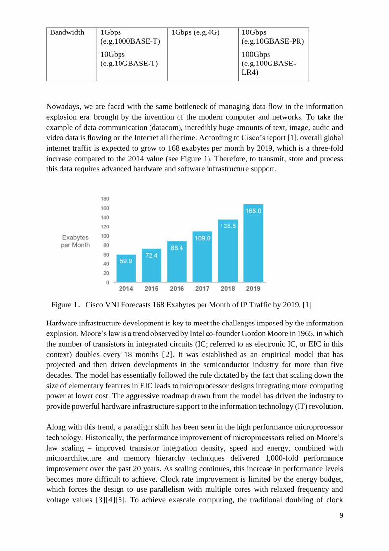
video data is flowing on the Internet all the time. According to Cisco’s report [1], overall global
internet traffic is expected to grow to 168 exabytes per month by 2019, which is a three-fold
increase compared to the 2014 value (see Figure 1). Therefore, to transmit, store and process
this data requires advanced hardware and software infrastructure support.
Hardware infrastructure development is key to meet the challenges imposed by the information
explosion. Moore’s law is a trend observed by Intel co-founder Gordon Moore in 1965, in which
the number of transistors in integrated circuits (IC; referred to as electronic IC, or EIC in this
context) doubles every 18 months [2]. It was established as an empirical model that has
projected and then driven developments in the semiconductor industry for more than five
decades. The model has essentially followed the rule dictated by the fact that scaling down the
size of elementary features in EIC leads to microprocessor designs integrating more computing
power at lower cost. The aggressive roadmap drawn from the model has driven the industry to
provide powerful hardware infrastructure support to the information technology (IT) revolution.
Along with this trend, a paradigm shift has been seen in the high performance microprocessor
technology. Historically, the performance improvement of microprocessors relied on Moore’s
law scaling – improved transistor integration density, speed and energy, combined with
microarchitecture and memory hierarchy techniques delivered 1,000-fold performance
improvement over the past 20 years. As scaling continues, this increase in performance levels
becomes more difficult to achieve. Clock rate improvement is limited by the energy budget,
which forces the design to use parallelism with multiple cores with relaxed frequency and
voltage values [3][4][5]. To achieve exascale computing, the traditional doubling of clock
Figure 1.Cisco VNI Forecasts 168 Exabytes per Month of IP Traffic by 2019. [1]
10
speeds every 18-24 month is being replaced by a doubling of cores, threads or other parallelism
mechanisms. It cannot be realized without an efficient way of moving data between the cores
[6]. As pointed out some years ago by Miller D. et al. [7], there is a limit on the bit-rate capacity
of electrical interconnects that depends only on the “aspect ratio” of the interconnect, i.e., the
ratio of interconnect length to the square root of its total cross-sectional area. Multi-processing
unit architectures require high aspect ratio interconnects, while scaling does not impact this
factor. As a consequence, high speed and large scale computing systems are limited by
interconnect bandwidth capacity [ 8 ]. On the other hand, what does scale with smaller
interconnect is the energy dissipation [9][10], which rises with every technology node and
imposes higher constraints on the power budget of the design.
As early as 1984, Goodman J.W. et al. [11] predict and propose the future usage of an optical
link as intra-chip, inter-chip and inter-board communication to replace copper metallic
communication media. Optical links can potentially defeat their electrical counterparts with
high speed, high bandwidth, low energy dissipation and electromagnetic immunity, as well as
other benefits. When interconnect bandwidth and power concerns became a reality in many-
core architectures for high performance computing (HPC) applications, using light to route
signal around the chip emerges as an increasingly attractive option over copper-based
interconnects that is potentially able to resolve the bottleneck [12].
2015 is the 50th year since the Moore’s law was formulated, and in the past decades there have
been debates over whether the industry can or should continue to follow the model – it remains
questionable whether squeezing more and smaller transistors into chips can really bring better
performance or economic return at advanced technology nodes. For example, with 22-
nanometer transistor feature sizes, the power consumption constraint starts to limit further chip
clock rate improvement; and to upgrade the design and fabrication infrastructure requires
investments that are greater than ever [13].
To adjust the model according to new technology limitations and economic constraints,
Moore’s law has been divided into “More Moore” and “More than Moore” [14][15][16]. The
former focuses on further scaling with CMOS or with alternative options (materials, processes
and device structures); and the latter aims at integrating more functions into the system. The
main driver for the semiconductor business during the 80s and 90s was the performance and
cost expectations of the memories and microprocessors. However, since the beginning of the
21st century, systems-on-chip (SoC) and systems-in-package (SiP) have emerged as design
houses have started to make customized designs rather than standard components to address
specific applications. As applications evolve, they drive further requirements for heterogeneous
integration – the key goal becomes realizing a system that meets the technology requirements
for a specific application. New requirements emerge from applications such as data centers,
mobility, context-aware computing [17], and they appear as the new driver for EIC products
that contribute to shaping the future evolution of the semiconductor industry.
The afore-mentioned technology and industry paradigm shift has brought great opportunity to
optics. The insertion of photonics in on-chip global interconnect structures can leverage the
unique advantages of optical communication that has already benefited applications such as
long-haul and metropolitan networks. Intra-chip optical links have been reviewed in [18] by
11
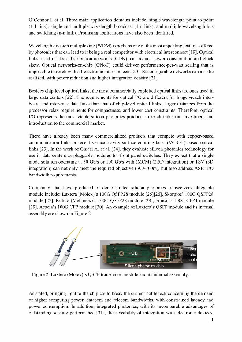
O’Connor I. et al. Three main application domains include: single wavelength point-to-point (1-1 link); single and multiple wavelength broadcast (1-n link); and multiple wavelength bus and switching (n-n link). Promising applications have also been identified. Wavelength division multiplexing (WDM) is perhaps one of the most appealing features offered by photonics that can lead to it being a real competitor with electrical interconnect [19]. Optical links, used in clock distribution networks (CDN), can reduce power consumption and clock skew. Optical networks-on-chip (ONoC) could deliver performance-per-watt scaling that is impossible to reach with all-electronic interconnects [20]. Reconfigurable networks can also be realized, with power reduction and higher integration density [21]. Besides chip level optical links, the most commercially exploited optical links are ones used in large data centers [22]. The requirements for optical I/O are different for longer-reach inter-board and inter-rack data links than that of chip-level optical links; larger distances from the processor relax requirements for compactness, and lower cost constraints. Therefore, optical I/O represents the most viable silicon photonics products to reach industrial investment and introduction to the commercial market. There have already been many commercialized products that compete with copper-based communication links or recent vertical-cavity surface-emitting laser (VCSEL)-based optical links [23]. In the work of Ghiasi A. et al. [24], they evaluate silicon photonics technology for use in data centers as pluggable modules for front panel switches. They expect that a single mode solution operating at 50 Gb/s or 100 Gb/s with (MCM) (2.5D integration) or TSV (3D integration) can not only meet the required objective (300-700m), but also address ASIC I/O bandwidth requirements. Companies that have produced or demonstrated silicon photonics transceivers pluggable module include: Luxtera (Molex)’s 100G QSFP28 module [25][26], Skorpios’ 100G QSFP28
module [27], Kotura (Mellanox)’s 100G QSFP28 module [28], Finisar’s 100G CFP4 module
[29], Acacia’s 100G CFP module [30]. An example of Luxtera’s QSFP module and its internal assembly are shown in Figure 2.
As stated, bringing light to the chip could break the current bottleneck concerning the demand of higher computing power, datacom and telecom bandwidths, with constrained latency and power consumption. In addition, integrated photonics, with its incomparable advantages of outstanding sensing performance [31], the possibility of integration with electronic devices,
Figure 2. Luxtera (Molex)’s QSFP transceiver module and its internal assembly.
PCB
Silicon photonics chip
Fiber-optic cable
12
compactness, metal-free operation, low-cost and electromagnetic immunity, is a good candidate
for sensing instrumentation in various applications such as industrial and space sensing,
biotechnology and bio-medical applications [32][33].
1.1.2 Leveraging silicon platform for integrated photonics
Since 1985 when pioneering studies found that single-crystal silicon can be used as optical
transmission media at telecom wavelength ranges (λ=1.3 and 1.55 μm) [ 34], integrating
photonics components using the CMOS platform has attracted interest from both research and
industry. The potential to leverage the considerable investments in the semiconductor industry
promises an economy of scale for the silicon photonics market and is consequently an attractive
return on investment. Also, the possibility of fabricating photonic circuits side-by-side with ICs
has actually inspired research in using silicon waveguides as intra-chip optical links and various
other applications as mentioned before. The following facts have made it possible to combine
photonic integrated circuits with silicon technology:
Si can serve as a waveguide at telecom wavelengths
SiO2 is naturally available, which serves as an excellent insulation and passivation
material; also, combined with Si, it provides high optical index difference for efficient
light confinement, which contributes to compact photonics circuit designs
Silicon-on-Insulator (SOI) wafers are available, which provide a SiO2 layer beneath the
Si
Mature CMOS platforms provide access to an immense infrastructure for yield
improvement, metrology and process control. This allows a high level of integration,
where photonic components are built within a single chip, as opposed to discrete optical
modules, and also allows the possibility to co-integrate electronic circuits with photonic
circuits on the same chip [35][36]. Combined with CMOS, MEMS, and 3D stacking
technologies, silicon photonics can bring forth a range of exciting applications as well
as performance improvement to the entire system.
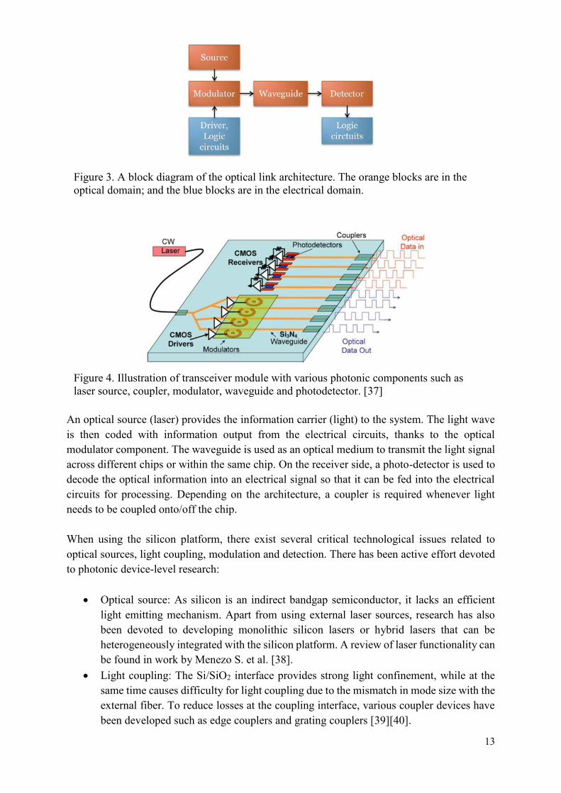
To build a photonic circuit or system, various active and passive components are required to
manipulate light on the chip. Examples include: laser sources, fiber/waveguide couplers,
waveguide interconnects, power splitters, modulators and detectors. These components can be
found in an optical link application, as illustrated in the block diagram in Figure 3 and a
transceiver module in Figure 4 [37].
13
An optical source (laser) provides the information carrier (light) to the system. The light wave is then coded with information output from the electrical circuits, thanks to the optical modulator component. The waveguide is used as an optical medium to transmit the light signal across different chips or within the same chip. On the receiver side, a photo-detector is used to decode the optical information into an electrical signal so that it can be fed into the electrical circuits for processing. Depending on the architecture, a coupler is required whenever light needs to be coupled onto/off the chip. When using the silicon platform, there exist several critical technological issues related to optical sources, light coupling, modulation and detection. There has been active effort devoted to photonic device-level research:
Optical source: As silicon is an indirect bandgap semiconductor, it lacks an efficient light emitting mechanism. Apart from using external laser sources, research has also been devoted to developing monolithic silicon lasers or hybrid lasers that can be heterogeneously integrated with the silicon platform. A review of laser functionality can be found in work by Menezo S. et al. [38].
Light coupling: The Si/SiO2 interface provides strong light confinement, while at the same time causes difficulty for light coupling due to the mismatch in mode size with the external fiber. To reduce losses at the coupling interface, various coupler devices have been developed such as edge couplers and grating couplers [39][40].
Figure 3. A block diagram of the optical link architecture. The orange blocks are in the optical domain; and the blue blocks are in the electrical domain.
Figure 4. Illustration of transceiver module with various photonic components such as laser source, coupler, modulator, waveguide and photodetector. [37]
14
Light modulation: Unstrained crystalline silicon does not exhibit a linear electro-optic
effect (Pockels effect). It is this mechanism that produces the refractive index change of
material and is key to controlling transmission properties in the photonic devices,
thereby controlling the flow of light in the circuit (components performing such
functions include modulators and switches). Similar to the laser and photodetector, two
general paths of development are pursued: one based on exploring alternative
modulation mechanisms with silicon [ 41 ], the other based on the integration of
alternative materials such as germanium [42].
Light detection: The transparency of silicon material at a given operational wavelength
also implies the fact that photodetection cannot be done (or can only be done very
inefficiently) with the same material. Popular solutions include photodetector devices
based on germanium integration [43], and III-V heterogeneous integration [44].
The above mentioned issues have been widely studied and significant success has been achieved
in device innovation and optimization, driven by the promise of low cost and high volume of
silicon photonics. Evaluations of various metrics such as efficiency/loss and cost are key to
enable a silicon photonics system that can justify its performance superiority over traditional
copper-based methods, discrete optical component-based methods, or other integrated
photonics technologies. Other photonic integrated circuit (PIC) platforms include glass,
polymer, III-V compounds (like InP and GaAs), etc. Some technologies can be stand-alone
platforms; technologies are also exploited as heterogeneously integrated on a silicon substrate;
and the rest takes silicon material on its substrate [45].
The InP platform is the most competitive technology against Si photonics [46][47]. Because of
its efficient mechanism for photon-electron conversion, it is possible to integrate both passive
and active components (such as laser, modulator and detector) onto the same die. In contrast,
laser integration is more complex with silicon; and in order to create a photodetector on a Si
chip, alternative process steps are required like Germanium. However, compared to the Si
platform, InP does not hold the advantage of maturity and is not as widely available. Also, the
waveguide interface characteristics (Si/SiO2) provided by silicon technology allow very narrow
waveguides to be built, which results in a much smaller circuit footprint than that provided by
InP.
The two technologies find their positions in the current market by the balance of performance
and cost. InP-based components are mainly adopted in telecommunication markets (relatively
smaller market size and higher performance requirements). In other applications such as data
centers and computing applications, the market is extremely sensitive to cost while some
performance can be sacrificed because the communication distance is smaller [ 48 ]. No
semiconductor can compete with Si in terms of cost and device size, and it has a better chance
to win these markets. As its potential of CMOS compatibility promises a significant cost
advantage, research effort and investment continue to drive silicon photonics. Therefore, it is
not unrealistic to expect that silicon photonics can deliver equally good or even better
performance than its counterpart.
15
1.1.3 Challenges ahead
Potential compatibility with the standard CMOS process is the primary advantage offered by
the silicon photonics technology. However, bringing the design concepts from research to
volume production requires a collective effort from the scientific and industrial communities.
There are various investment activities in this field over the past years that have pursued the
industrialization of the technology:
Existing telecom and datacom companies continue to explore this alternative technology in
addition to their existing solutions. This can be done with:
o Dedicated research and development, usually in collaboration with research institutes.
These include system providers like IBM, NTT, Oracle, HP, Alcatel-Lucent, Fujitsu;
module providers such as Intel, STMicroelectronics, Corning, Acacia Communications,
Chiral Photonics, TeraXion, Finisar, Omega Optics.
o Acquisition of existing silicon photonics companies: BinOptics and Photonic Controls
by M/A-COM [49][50]; Caliopa by Huawei [51]; CyOptics by Avago [52]; Kotura by
Mellanox [53]; Lightwire by Cisco Systems [54]; Luxtera’s silicon photonics-based
active optical cable (AOC) business by Molex [55].
Companies that debut with their proprietary silicon photonics technologies, including:
o Those that have been acquired by telecom and datacom companies mentioned
previously;
o Other companies like Skorpios, Aurrion, Compass-EOS, etc.
Government investment has also seen a rise in the past few years world-wide which supports
research projects involving academic and/or industrial efforts:
o European projects such as the currently running Photonic Libraries And Technology
for Manufacturing (Plat4M) (2012) [56], pHotonics ELectronics functional Integration
on CMOS (Helios) (2008) [57];
o US projects such as the current Integrated Photonics Institute for Manufacturing
Innovation (IP-IMI) (2015) [ 58 ], Ultraperformance Nanophotonic Intrachip
Communication (UNIC) (2007) [59];
o Japanese research association Photonics and Electronics Converged Devices and
Systems (PETRA) (2009) [60] which runs several projects;
o Chinese research programs under 973 [61] and 863 [62] project.
Despite the significant cost advantage gained through the prospect of economy of scale,
accessing CMOS facilities is difficult. Developing a custom silicon photonics process requires
huge investment. Big industrial leaders – integrated device manufacturers (IDMs), and
academic institution leaders are able to develop their own fabs and processes to perform in-
house manufacturing. Further, some of them provide their manufacturing capability to design
houses as a foundry service. This is similar to the eco-system that was formed in the
semiconductor industry as the so-called “fabless-foundry” model. The foundry can either be
part of the IDM business, or as a pure-play foundry.
16
Such an eco-system appeared as semiconductor technology became more and more complex,
and a focused effort on either design or fabrication became the key to the success of a
semiconductor company. The outcome is that it further revolutionized the industry by dividing
highly specialized tasks; and the fact that design innovations were encouraged by the
decoupling of expensive fabrication from fabless companies. The silicon photonics community
can also benefit from such an eco-system [63][64].
Prior to commercial fabrication, there also exists a gap to be bridged between academic research
and expensive manufacturing facilities. The semiconductor industry has also created a model
to help small organizations to reach industry-level platforms through so-called multi-project
wafer (MPW) runs, where wafer space and fabrication costs of prototype designs are shared
between multiple users. Listed below are MPW shuttle runs and custom run facilities for silicon
photonics technology. A review of some of the foundry silicon photonics technologies can be
found in a report by Lim A.E.-J. [65] :
MPW shuttle run:
Imec, CEA-Leti, Global Foundries, IHP, VTT, BAE Systems, accessed either through their
own organization, or through MPW service brokers like EUROPRACTICE, CMC, and
MOSIS. These projects and services also organize silicon photonics design training programs
(like SiEPIC [66] and ePIXfab [67][68] workshop).
Foundry custom run:
In addition to the above-mentioned MPW shuttle runs provided by foundries that have
developed silicon photonics manufacturing, there are also a few foundries that already
collaborate with specific customers for customized processes and runs: Freescale
[69][70][71], STMicroelectronics [72][73], Global Foundries [74], Texas Instrument [75]
and undisclosed foundry partners of a few design companies.
As a result of the growing eco-system, start-up fabless silicon photonics companies are
appearing rapidly: VLC Photonics, OneChip, Rockley Photonics, etc.
CMOS compatibility has been a hot topic of industrial investigation [76][77], proved with many
successful demonstrations like the above-mentioned industrial or academic organizations.
Another key challenge lies on the design tool side. Leveraging the CMOS infrastructure for
silicon photonics means not only including the re-use of manufacturing facilities, but also of
design tools with flow compatibility. Automated design tools and flows which are highly
coupled to the entire chip production process, is the key enabler of the modern semiconductor
industry. It ensures the scalability and reliability of EIC design and manufacturing. Therefore,
in order to be able to port silicon photonics designs to CMOS platforms, as well as to fully
benefit from its efficiency and guarantee of yield, the software tool infrastructure must be
assessed for silicon photonics design capability.
17
1.2 Design Tools for PIC
1.2.1 CAD tools for photonic designs
Computer-aided design (CAD) is the use of computer systems to assist in the creation,
modification, analysis, or optimization of a design. As in many industrial fields, photonic
component designers rely on dedicated software tools that exploit the computing power of the
machine to realize their design concepts. They create the component designs virtually,
formulate the operating conditions, run simulations based on certain algorithms, and visualize
and analyze the results.
Most of the existing commercial photonics CAD tools are dedicated to physical level simulation.
They help designers create and optimize photonic building block designs based on physical
model simulations (device geometry, topography, material properties, etc.). These tools offer a
range of modeling and simulation solutions based on different computation methods, dedicated
to time domain or frequency domain analysis [78][79][80][81]:
Finite-difference time-domain (FDTD) which solves Maxwell equations numerically;
Beam propagation method (BPM) which solves an approximation of the exact wave
equation;
Eigenmode Expansion (EME) which simulates electromagnetic propagation by solving
Maxwell's equations in each local cross-section of the device;
Methods of lines (MoL) which is a semi-analytical algorithm that solves partial
differential equations;
Coupled mode theory (CMT), transfer matrix methods (TMM), and Floquet-Bloch
theory (FBT) methods, which are used for analysis of periodic structures like photonic
crystals and distributed feedback lasers (DFB).
These tools are often known as TCAD (Technology CAD), and they are available from:
Commercial companies like Lumerical, PhoeniX Software, Luceda Photonics,
Synopsys RSoft, Photon Design, OptiWave, VPIphotonics, RP Photonics, Weidlinger,
JCMwave, Appollo Photonics, PHOTOSS, Simphotek, Silvaco, and COMSOL;
Free software tools like MEEP, CAMFR, IPKISS, EM Explorer, SiIO, 2D-Waveguide,
LIGHTS, MIT Photonic Bands, MOF, openEMS, RODIS, WAVEGUIDE and
WOLFSIM.
With the device models resolved, process device parameters and operating conditions can be
fed into the model and the output is produced which is monitored by instrumentation or drives
other models.
Physical level simulation is intended to be accurate and often takes a long time, and is thus not
suitable for circuit- or system-level design. However, it is essential to device level design and
technology development – device designers use these techniques to create novel devices or to
optimize existing devices. Once the physical characteristics of the components are defined, the
device design and process technology can be considered as frozen. Compact models can then
18
be created which are suitable for the simulation of large and complex circuits or systems.
Compact models are built based on physical models, theory, and parameters extracted from
measurements, and are expressed as analytical equations or scattering matrices (s-matrix)
[82][83]. Using such models, circuit simulation can be performed with balanced accuracy and
runtime. The following tools provide photonic circuit simulation capability:
Commercial photonic circuit simulation engines like Lumerical INTERCONNECT,
ASPIC, Caphe, Optiwave OptiSystem, Photon Design PICWave, RSoft OptSim Circuit
and ModeSYS, VPIsystems VPItransmissionMaker and VPIcomponentMaker Photonic
Circuit;
Verilog-A is also an industry standard modeling language for analog electrical circuits.
Photonic device behavioral models can be represented by Verilog-A, and the circuit is
then simulated with commercial SPICE (Simulation Program with Integrated Circuit
Emphasis) simulators. Electrical and optical characteristics are captured from the circuit
simultaneously [84][85][86][87], and this method offers the advantage of co-simulating
the electro-optical circuit in an EDA standard environment.
The availability of compact device models enables the design at a higher abstraction level
compared to physical device modeling. High-level means being more abstract and low-level
means being more detailed: for example, designing a circuit at register-transfer level (RTL)
using Verilog language, versus designing a circuit from the transistor level. From high-level to
low-level, simulation becomes more accurate, as well as progressively more complex and time-
consuming. Circuit designers can directly use created photonic devices to create circuits without
starting from the bottom physical level [88].
Depending on applications, modeling and design at the circuit level can suffice, for example,
for a small circuit such as a 4-channel optical transceiver, which is composed of a few tens of
photonic devices. However, when larger and more complex designs appear, design
methodologies at a higher abstraction level are needed. It is not possible to create a complex
design such as an ONoC without the help of high level (system/network/architecture level)
design, simulation and analysis tools [89]. Available photonic system and network simulation
environments include [90]:
Commercial tools like RSoft OptSim, as well as free tools like OMNeT++, PhoenixSim
and MIT-DSENT;
Integration of optical network models with generic system hardware simulation
languages such as SystemC, which is an abstract modeling language.
There are also system-level design tools for physical synthesis and optimization, such as
Columbia's Optical Interconnect Library (OIL), a synthesis-like tool for latency and insertion
loss optimization [91]; Minz J.R. et al. [92] presented a synthesis tool for timing and congestion-
driven waveguide routing optimization; PROTON [93] is a place-and-route (P&R) for ONoC
optical components which is able to minimize propagation and crossing loss; VANDAL [94] is
also a P&R tool for on-chip photonic architectures which uses a library of modeled and
characterized components, and includes automation tools for rapid design and synthesis.
O’Connor I. [95] presented a link-level simulation environment for heterogeneous photonic
19
integrated circuits which leverages detailed synthesizable models of building-block components
for the purpose of determining interconnect density, area, link delay, and link power
requirements.
Most of the above reviewed photonic CAD tools are dedicated to designs at a specific
abstraction level: device, circuit, system or architecture; and currently researchers and designers
use a combination of these individual tools to realize a design. Research in photonic device
optimization has made a lot of progress and is an active area. Circuit and system designers not
only concentrate on their own field of expertise, but also keep a close eye on the latest
advancements in device innovation so that they can improve their designs with updated
component specifications. In fact, most photonic designers are much like analog electronic
circuit designers: they build the circuit from the device construction – a bottom-up approach.
This comes from two aspects:
Most photonic circuit designs need careful phase engineering which depends on how
the waveguides are routed. Parasitic effects such as crosstalk and loss must be avoided
or minimized, and designers therefore need to be aware of device physics in addition to
circuit or system design knowledge;
There lacks an integrated design and data flow, which is able to bridge the designs at
different abstraction levels in an efficient way – currently, design construction is mostly
manual and design data is also managed manually.
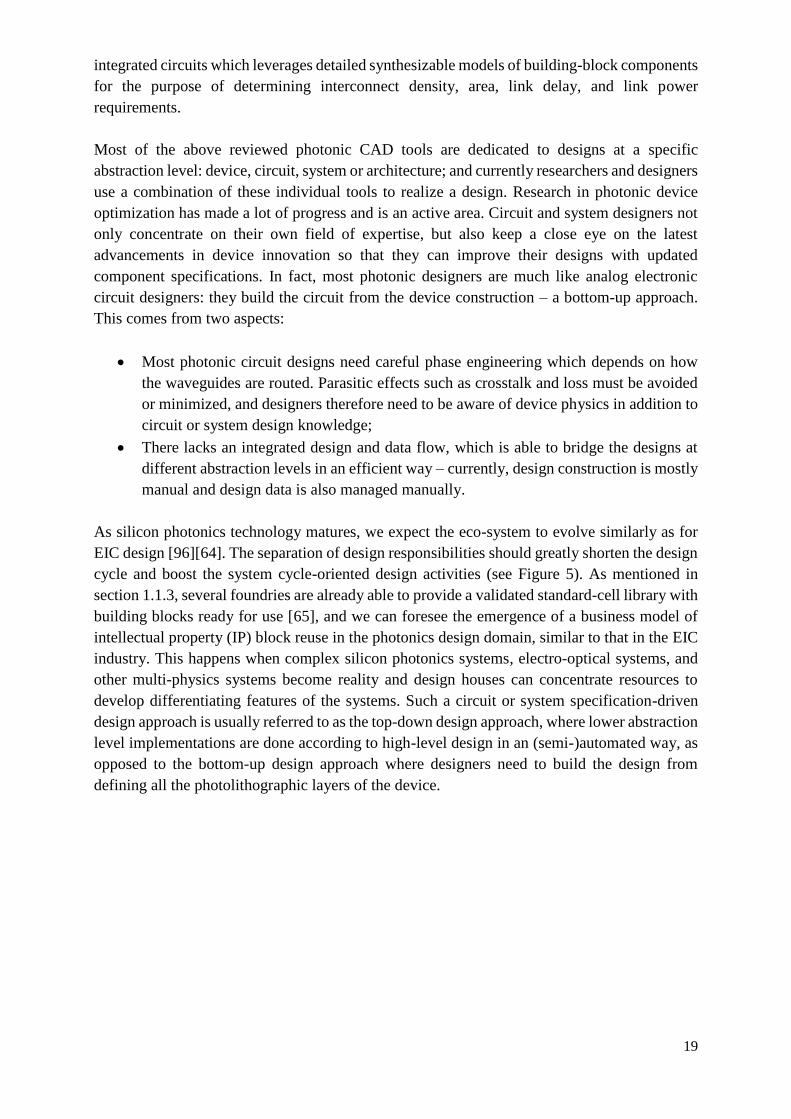
As silicon photonics technology matures, we expect the eco-system to evolve similarly as for
EIC design [96][64]. The separation of design responsibilities should greatly shorten the design
cycle and boost the system cycle-oriented design activities (see Figure 5). As mentioned in
section 1.1.3, several foundries are already able to provide a validated standard-cell library with
building blocks ready for use [65], and we can foresee the emergence of a business model of
intellectual property (IP) block reuse in the photonics design domain, similar to that in the EIC
industry. This happens when complex silicon photonics systems, electro-optical systems, and
other multi-physics systems become reality and design houses can concentrate resources to
develop differentiating features of the systems. Such a circuit or system specification-driven
design approach is usually referred to as the top-down design approach, where lower abstraction
level implementations are done according to high-level design in an (semi-)automated way, as
opposed to the bottom-up design approach where designers need to build the design from
defining all the photolithographic layers of the device.
20
Whether the design is performed with a top-down or a bottom-up approach, corresponding design automation methods and integrated design environments are indispensable. They are the key to
Filling the gap between technology offerings and circuit and system design innovations; Improving design process efficiency by separation of responsibilities – designers work
in their field of expertise on device, circuit, system or physical layout; potential failures can also be better managed within this modular workflow.
In this section, we have introduced the current status of silicon photonics CAD tools, most of which are highly specialized at a certain abstraction level; and we identified one of the most important challenges preventing photonic designers today from designing as efficiently and reliably as in the EIC industry, as the lack of a mature design automation flow. In the next section, we will introduce the concept of EDA, which is a CAD methodology in the EIC domain. We will review current efforts in leveraging the EDA methodology for photonic designs, and the promise of its impact (as it contributes to the success of the EIC industry). In the next chapter, we will concentrate on a key part in an EDA design flow – the physical verification stage – and analyze the challenges in its adoption for the PIC design.
1.2.2 Leveraging EDA for photonic designs EDA is a category of CAD tools that is specialized in the design of EIC chips. It includes a large collection of software tools that enhance and aid the development of complex electronic systems. Before EDA, integrated circuits were designed by hand and manually laid out. In fact, the success of the EIC industry is largely due to the development of the EDA approach. Software tools were developed to automate the design. This includes design and place-and-route tools that help draft the design from electronics to graphics; techniques which use programming
a) b)
Figure 5. a) Traditional photonic design approach: single designer using multiple individual CAD tools to perform design at various abstraction levels. b) Integrated photonic design flow: different designers performing dedicated tasks at different abstraction levels within an integrated design environment.
21
language to describe a design concept, and compile it to silicon; as well as design verification
tools. As an immediate outcome, designs were easier to layout, and more likely to function
correctly with the thorough application of simulation and verification tools during all stages of
design prior to fabrication. Very-large-scale integration (VLSI) EIC design is today not possible
without the help of these software tools. Throughout its history, EDA development has gone
hand in hand with EIC technology advancement. Following the trend of migrating to the next
generation or next technology "node", there is increasing demand for more advanced EDA tools.
The EDA technique is a key part of the semiconductor infrastructure and is integral to the
semiconductor industry.
We indicated in section 1.1 “Silicon Photonics” that significant success has been made in silicon
photonics technology, especially in the areas of device innovation and technology integration,
and has already demonstrated successful products. A critical remaining challenge is to bring the
technology to a level that can compete with other traditional and alternative technologies, or
prove that the introduction of silicon photonics can really bring performance improvements that
justify the additional cost. The key to shift the industry choice towards the silicon photonics
technology is thus whether it can deliver its promise of CMOS platform reuse, and it depends
on the maturity of the ecosystem, where a similar fabless model as in EIC industry can guarantee
productivity and investment effectiveness that lets small fabless companies access
semiconductor design.
Historically, EDA has enabled the EIC industry to follow a rapid development phase, by
automating the design, verification, and testing flows of the EIC chips. Without its contributions,
the ICs that today comprise billions of transistors would not have been possible. Along with the
fabless revolution, commercial EDA made it possible for hundreds of companies to design
semiconductors, as opposed to the very few that could afford large internal CAD operations and
fabs. It has brought forth plenty of creativity and EICs have reached a new level of
sophistication and intelligence. The same holds true for PIC – in order to duplicate the success
of the EIC industry for PICs, the industry must fully adapt the technology platform, including
the usage of automation tools that address photonic-specific requirements. On the other hand,
it is also economically beneficial to leverage the existing well-developed EDA tool suite and
design flows, which also represents significant industry investments. The semiconductor
ecosystem is used to well-developed methodologies and design flows developed together
between EDA tool vendors and their customers (design houses, foundries, and IDMs).
Therefore, the reuse of the CMOS platform for PIC not only means the integration of fabrication
technology, but also the reuse of tools and integration of design flow. Moreover, due to the wide
industrial adoption and the maturity of EDA technology, it can be leveraged for photonic
designs that promise high efficiency and quality in design, and high yield and reliability in
manufacturing.
Therefore, we identified that one of the key success factors for the silicon photonics industry
lies in whether it can leverage the existing EDA infrastructure.
1.2.3 The EDA methodology and the PDK
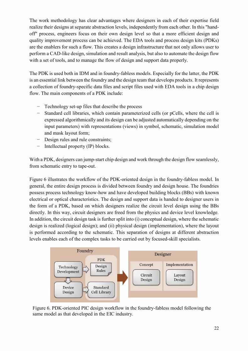
22
The work methodology has clear advantages where designers in each of their expertise field realize their designs at separate abstraction levels, independently from each other. In this "hand-off" process, engineers focus on their own design level so that a more efficient design and quality improvement process can be achieved. The EDA tools and process design kits (PDKs) are the enablers for such a flow. This creates a design infrastructure that not only allows user to perform a CAD-like design, simulation and result analysis, but also to automate the design flow with a set of tools, and to manage the flow of design and support data properly. The PDK is used both in IDM and in foundry-fabless models. Especially for the latter, the PDK is an essential link between the foundry and the design team that develops products. It represents a collection of foundry-specific data files and script files used with EDA tools in a chip design flow. The main components of a PDK include:
− Technology set-up files that describe the process − Standard cell libraries, which contain parameterized cells (or pCells, where the cell is
expressed algorithmically and its design can be adjusted automatically depending on the input parameters) with representations (views) in symbol, schematic, simulation model and mask layout form;
− Design rules and rule constraints; − Intellectual property (IP) blocks.
With a PDK, designers can jump-start chip design and work through the design flow seamlessly, from schematic entry to tape-out. Figure 6 illustrates the workflow of the PDK-oriented design in the foundry-fabless model. In general, the entire design process is divided between foundry and design house. The foundries possess process technology know-how and have developed building blocks (BBs) with known electrical or optical characteristics. The design and support data is handed to designer users in the form of a PDK, based on which designers realize the circuit level design using the BBs directly. In this way, circuit designers are freed from the physics and device level knowledge. In addition, the circuit design task is further split into (i) conceptual design, where the schematic design is realized (logical design); and (ii) physical design (implementation), where the layout is performed according to the schematic. This separation of designs at different abstraction levels enables each of the complex tasks to be carried out by focused-skill specialists.
Figure 6. PDK-oriented PIC design workflow in the foundry-fabless model following the same model as that developed in the EIC industry.
23
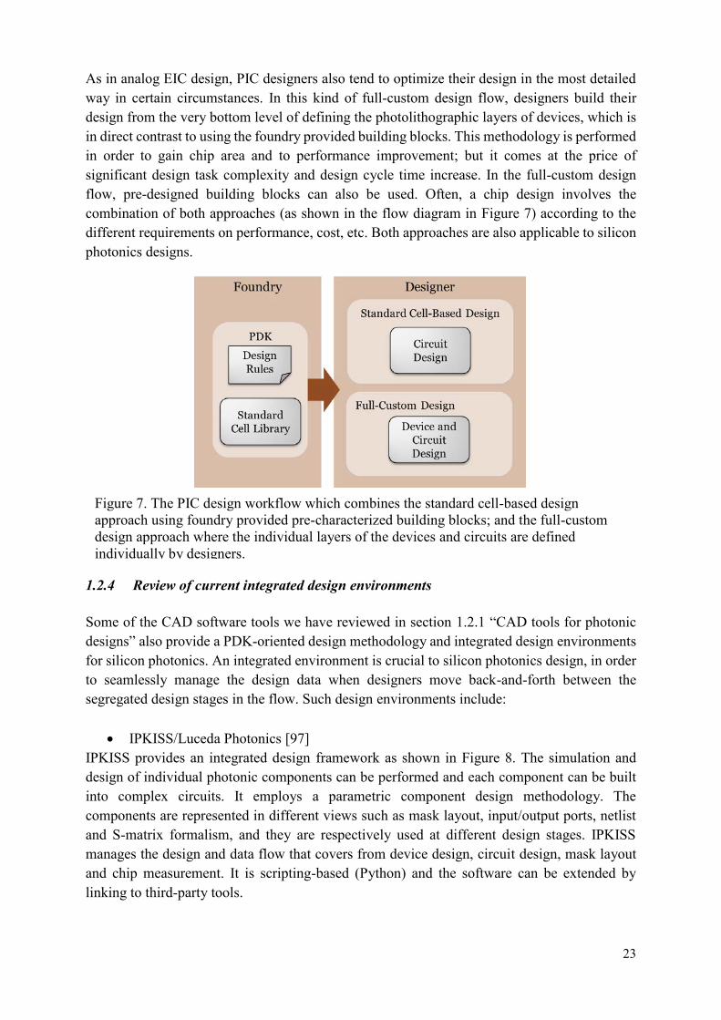
As in analog EIC design, PIC designers also tend to optimize their design in the most detailed way in certain circumstances. In this kind of full-custom design flow, designers build their design from the very bottom level of defining the photolithographic layers of devices, which is in direct contrast to using the foundry provided building blocks. This methodology is performed in order to gain chip area and to performance improvement; but it comes at the price of significant design task complexity and design cycle time increase. In the full-custom design flow, pre-designed building blocks can also be used. Often, a chip design involves the combination of both approaches (as shown in the flow diagram in Figure 7) according to the different requirements on performance, cost, etc. Both approaches are also applicable to silicon photonics designs.
1.2.4 Review of current integrated design environments Some of the CAD software tools we have reviewed in section 1.2.1 “CAD tools for photonic designs” also provide a PDK-oriented design methodology and integrated design environments for silicon photonics. An integrated environment is crucial to silicon photonics design, in order to seamlessly manage the design data when designers move back-and-forth between the segregated design stages in the flow. Such design environments include:
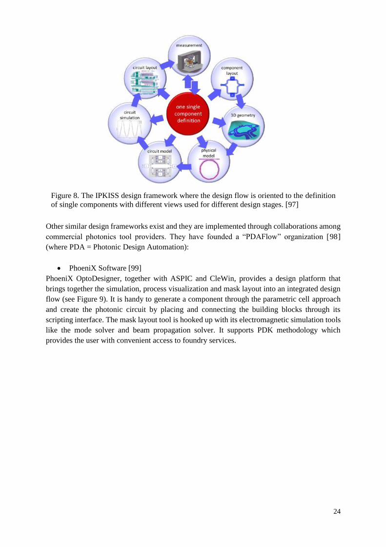
IPKISS/Luceda Photonics [97] IPKISS provides an integrated design framework as shown in Figure 8. The simulation and design of individual photonic components can be performed and each component can be built into complex circuits. It employs a parametric component design methodology. The components are represented in different views such as mask layout, input/output ports, netlist and S-matrix formalism, and they are respectively used at different design stages. IPKISS manages the design and data flow that covers from device design, circuit design, mask layout and chip measurement. It is scripting-based (Python) and the software can be extended by linking to third-party tools.
Figure 7. The PIC design workflow which combines the standard cell-based design approach using foundry provided pre-characterized building blocks; and the full-custom design approach where the individual layers of the devices and circuits are defined individually by designers.
24
Other similar design frameworks exist and they are implemented through collaborations among
commercial photonics tool providers. They have founded a “PDAFlow” organization [98]
(where PDA = Photonic Design Automation):
PhoeniX Software [99]
PhoeniX OptoDesigner, together with ASPIC and CleWin, provides a design platform that
brings together the simulation, process visualization and mask layout into an integrated design
flow (see Figure 9). It is handy to generate a component through the parametric cell approach
and create the photonic circuit by placing and connecting the building blocks through its
scripting interface. The mask layout tool is hooked up with its electromagnetic simulation tools
like the mode solver and beam propagation solver. It supports PDK methodology which
provides the user with convenient access to foundry services.
Figure 8. The IPKISS design framework where the design flow is oriented to the definition
of single components with different views used for different design stages. [97]
25
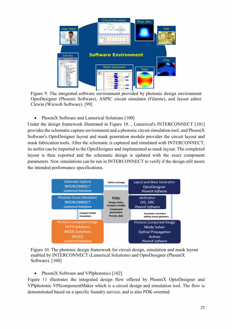
PhoeniX Software and Lumerical Solutions [100] Under the design framework illustrated in Figure 10. , Lumerical's INTERCONNECT [101] provides the schematic capture environment and a photonic circuit simulation tool; and PhoeniX Software's OptoDesigner layout and mask generation module provides the circuit layout and mask fabrication tools. After the schematic is captured and simulated with INTERCONNECT, its netlist can be imported to the OptoDesigner and implemented as mask layout. The completed layout is then exported and the schematic design is updated with the exact component parameters. New simulations can be run in INTERCONNECT to verify if the design still meets the intended performance specifications.
PhoeniX Software and VPIphotonics [102]
Figure 11 illustrates the integrated design flow offered by PhoeniX OptoDesigner and VPIphotonic VPIcomponentMaker which is a circuit design and simulation tool. The flow is demonstrated based on a specific foundry service, and is also PDK-oriented.
Figure 9. The integrated software environment provided by photonic design environment OptoDesigner (Phoenix Software), ASPIC circuit simulator (Filarete), and layout editor Clewin (Wieweb Software). [99]
Figure 10. The photonic design framework for circuit design, simulation and mask layout enabled by INTERCONNECT (Lumerical Solutions) and OptoDesigner (PhoeniX Software). [100]

26
IPKISS/Luceda Photonics and Tanner EDA [103],
Tanner is an EDA company that develops a full design tool flow. Its product extends to
applications such as analog and mixed-signal circuits, MEMS, and silicon photonics. MEMS
design is similar to photonics design in term of its all-angle and curvilinear layout. To deal with
the non-Manhattan layout, Tanner’s L-Edit offers powerful editing capabilities, such as defining
circles, arc and curves, and component rotation at any angle. By linking the photonics
component simulation and design flow of IPKISS to Tanner’s advanced layout editing
environment, they provide an integrated PIC design solution.
The above reviewed integrated design flows dedicated to PIC designs are mostly driven by
photonics tool providers. A similar design methodology as for EIC is often referred to as
photonic design automation (PDA). These tools are specialized in photonic modeling and
simulations, so they usually have powerful front-end design capability (like IPKISS, Lumerical
and PhoeniX); however, the back-end design flow is usually complemented by bringing in EDA
software (like Tanner’s L-Edit) into the flow. In the meantime, there are also efforts from the
EDA community to embrace photonics inside existing design platforms. Compared to the PDA
flow, the EDA-oriented flow offers several advantages: EDA tool developments have been
heavily invested. The EDA methodology is an inseparable part of the CMOS platform –
historically, the design is only valid for foundry access if it is performed by using the qualified
Figure 11. The design framework enabled by VPIcomponentMaker (VPIphotonics) and
OptoDesigner (PhoeniX Software) for photonic design, simulation and mask layout. [102]
Figure 12. A non-Manhattan photonic layout design realized by Tanner EDA’s L-Edit
layout editor. [103]
27
EDA design tools and flows. Reusing mature EDA design flows is more economically viable
in terms of cost-saving for tool R&D, and promises better design efficiency and reliability. The
automation provided by PDA greatly improves design productivity with integrated design
environments. However, its level of maturity and flow integration cannot be compared with the
EDA software.
From the EDA point of view, because of the difference between fundamental physics of
photonics and electronics, the EDA tools that have been developed for ICs do not lend all of
their concepts to the PIC design methodology, especially at the front-end design stage. Bogaert
W. et al. [104] identifies several important aspects where EDA tools are challenged by
electronic and photonic co-design problems:
o The information an optical waveguide can carry, and which needs to be analyzed,
includes power, phase, wavelength, and mode (or a subset of these parameters
depending on the application). It is suggested that there is no straight-forward way of
incorporating the richness of photonic signals into a standard electrical circuit simulator;
and the better solution is to interface simulators for the electronic and photonic domain.
o Photonics design is multi-physics and it involves not only the optical domain, but also
temperature, electronic carrier density, and the intrinsic nonlinear optical effect of
silicon. The circuit modeling must take all these factors into consideration.
o Waveguide behavior is very sensitive to the actual geometry of the cross section – and
thus the process variability. Photonic circuit simulation with process variability can be
done with Monte-Carlo, but with many more effects than are covered in electronic
design.
Leveraging the EDA framework for photonics design was first demonstrated by Mentor
Graphics Pyxis design environment interfaced with photonics software tools [105]. This effort
has answered most of the front-end design requests raised previously by introducing the
photonic modeling and simulation capability of photonic tools into the EDA framework. The
back-end design (physical layout) is also enhanced as compared to classical EDA tool. The
physical implementation impact on the photonic circuit behavior is significant, such that it
requires careful validation and sometimes needs to be taken care of in early design stages.
Mentor Graphics Pyxis [105]
Mentor Graphics Pyxis is an IC design platform. It offers a mainstream EDA design
environment linked to photonic simulation software provided by Lumerical and PhoeniX to
create a unified design flow for silicon photonics (Figure 13).
28
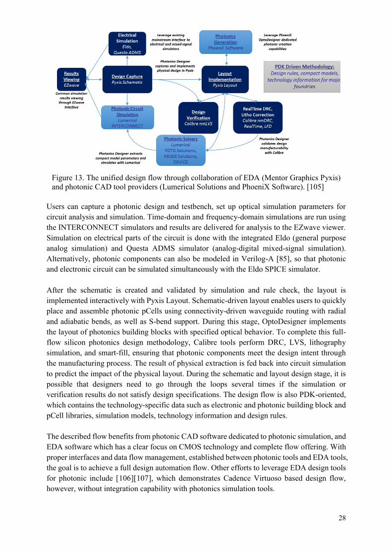
Users can capture a photonic design and testbench, set up optical simulation parameters for circuit analysis and simulation. Time-domain and frequency-domain simulations are run using the INTERCONNECT simulators and results are delivered for analysis to the EZwave viewer. Simulation on electrical parts of the circuit is done with the integrated Eldo (general purpose analog simulation) and Questa ADMS simulator (analog-digital mixed-signal simulation). Alternatively, photonic components can also be modeled in Verilog-A [85], so that photonic and electronic circuit can be simulated simultaneously with the Eldo SPICE simulator. After the schematic is created and validated by simulation and rule check, the layout is implemented interactively with Pyxis Layout. Schematic-driven layout enables users to quickly place and assemble photonic pCells using connectivity-driven waveguide routing with radial and adiabatic bends, as well as S-bend support. During this stage, OptoDesigner implements the layout of photonics building blocks with specified optical behavior. To complete this full-flow silicon photonics design methodology, Calibre tools perform DRC, LVS, lithography simulation, and smart-fill, ensuring that photonic components meet the design intent through the manufacturing process. The result of physical extraction is fed back into circuit simulation to predict the impact of the physical layout. During the schematic and layout design stage, it is possible that designers need to go through the loops several times if the simulation or verification results do not satisfy design specifications. The design flow is also PDK-oriented, which contains the technology-specific data such as electronic and photonic building block and pCell libraries, simulation models, technology information and design rules. The described flow benefits from photonic CAD software dedicated to photonic simulation, and EDA software which has a clear focus on CMOS technology and complete flow offering. With proper interfaces and data flow management, established between photonic tools and EDA tools, the goal is to achieve a full design automation flow. Other efforts to leverage EDA design tools for photonic include [106][107], which demonstrates Cadence Virtuoso based design flow, however, without integration capability with photonics simulation tools.
Figure 13. The unified design flow through collaboration of EDA (Mentor Graphics Pyxis) and photonic CAD tool providers (Lumerical Solutions and PhoeniX Software). [105]
29
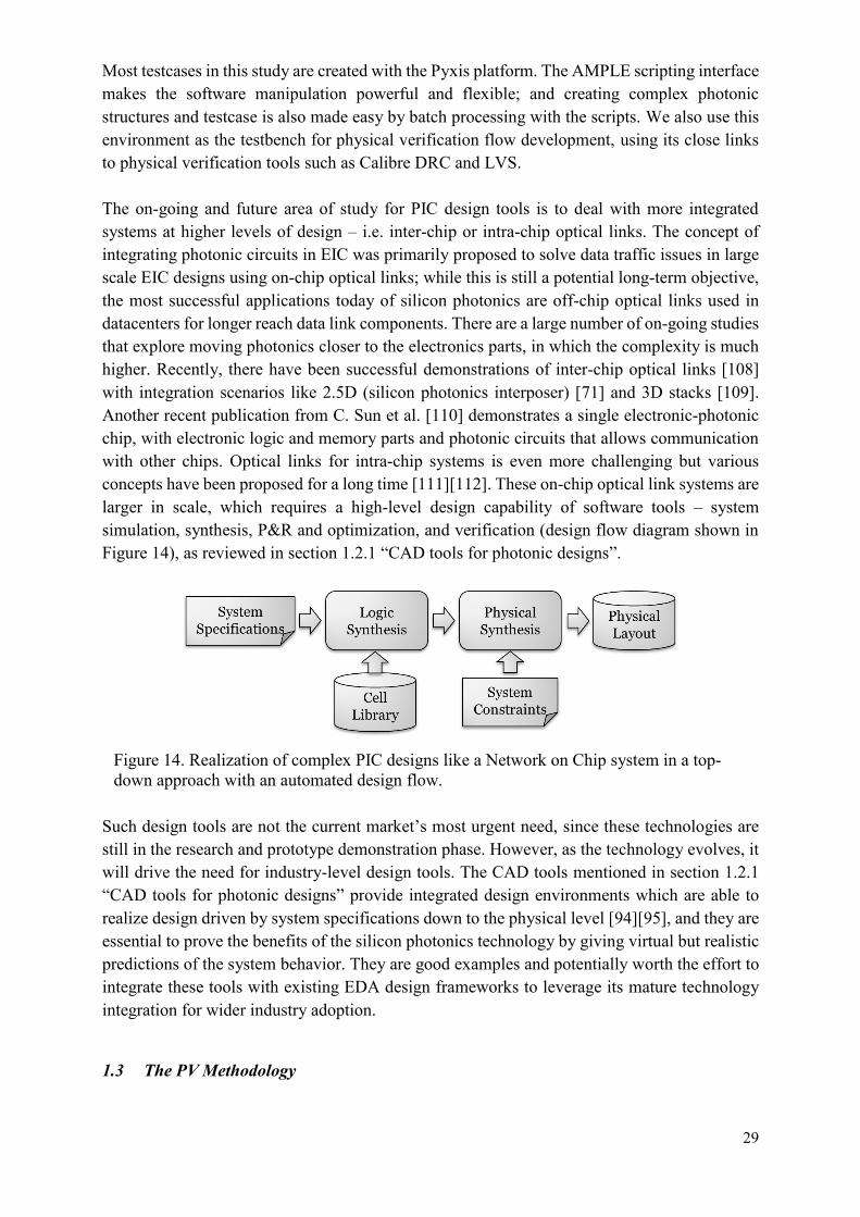
Most testcases in this study are created with the Pyxis platform. The AMPLE scripting interface makes the software manipulation powerful and flexible; and creating complex photonic structures and testcase is also made easy by batch processing with the scripts. We also use this environment as the testbench for physical verification flow development, using its close links to physical verification tools such as Calibre DRC and LVS. The on-going and future area of study for PIC design tools is to deal with more integrated systems at higher levels of design – i.e. inter-chip or intra-chip optical links. The concept of integrating photonic circuits in EIC was primarily proposed to solve data traffic issues in large scale EIC designs using on-chip optical links; while this is still a potential long-term objective, the most successful applications today of silicon photonics are off-chip optical links used in datacenters for longer reach data link components. There are a large number of on-going studies that explore moving photonics closer to the electronics parts, in which the complexity is much higher. Recently, there have been successful demonstrations of inter-chip optical links [108] with integration scenarios like 2.5D (silicon photonics interposer) [71] and 3D stacks [109]. Another recent publication from C. Sun et al. [110] demonstrates a single electronic-photonic chip, with electronic logic and memory parts and photonic circuits that allows communication with other chips. Optical links for intra-chip systems is even more challenging but various concepts have been proposed for a long time [111][112]. These on-chip optical link systems are larger in scale, which requires a high-level design capability of software tools – system simulation, synthesis, P&R and optimization, and verification (design flow diagram shown in Figure 14), as reviewed in section 1.2.1 “CAD tools for photonic designs”.
Such design tools are not the current market’s most urgent need, since these technologies are still in the research and prototype demonstration phase. However, as the technology evolves, it will drive the need for industry-level design tools. The CAD tools mentioned in section 1.2.1 “CAD tools for photonic designs” provide integrated design environments which are able to realize design driven by system specifications down to the physical level [94][95], and they are essential to prove the benefits of the silicon photonics technology by giving virtual but realistic predictions of the system behavior. They are good examples and potentially worth the effort to integrate these tools with existing EDA design frameworks to leverage its mature technology integration for wider industry adoption.
1.3 The PV Methodology
Figure 14. Realization of complex PIC designs like a Network on Chip system in a top-down approach with an automated design flow.
30
In section 1.2 “Design Tools for PIC”, we have discussed the software tool requirements for
realizing PIC designs, and reviewed the state-of-art of integrated design flows that help to port
the technology from research lab to industry. Design efficiency and cost constraints are
improved by leveraging the EDA methodology and environment; photonic simulation is
performed by integrating specialized CAD tools into the framework.
The design concept can be conducted effectively and correctly within the integrated design tool
framework. Nevertheless, this process involves a large amount of human intervention that can
induce error. Moreover, the manufacturing process can further deviate the printed silicon result
from the original design intent. After the initial design is realized, it is mandatory to validate at
various design stages whether there is human error or unacceptable levels of process-induced
distortion. In fact, the design cycle is closed for tape-out only after the design goes through the
physical verification (PV) flow. It is one of the key components of the EDA design flow.
A PV flow secures the design yield by checking essentially:
− If the design layout is appropriate for manufacturing given the target foundry or fab;
− If the design layout implementation meets the original design intent (conceptual design).
The PV flow has been well-developed to answer those questions for electronic design, i.e.
securing the design and fabrication yield of extremely large scale and complex EIC design at
advanced technology nodes that impose unprecedented verification challenges. There are a
number of components from the traditional CMOS physical verification world that can be
borrowed. All, however, will require some modification. The purpose of this study is to analyze
the PV requirements for photonic designs, and propose solutions to accomplish a reliable PV
flow that is able to secure photonic design yield. As we introduce new PV requirements, these
in turn also introduce new requirements to the upstream design flow.
Design for manufacturing (DFM) or early manufacturing involvement (EMI) will also be
discussed. These concepts are not new in industrial product design – in the case of the EIC
industry, it has adopted this methodology to meet the trend of rapid increase of technology
complexity. DFM allows potential manufacturing-related problems to be fixed in the design
phase, which is the least expensive place to address them. In the EIC domain, it addresses the
yield dropout issues such as random defects due to impurities, systematic defects contributed
by lithographic limitation and density induced planarity issues, etc.
The main tasks associated with PV and DFM can vary slightly from process to process but
typically consist of the following: design rule checking (DRC), fill insertion, layout vs.
schematic (LVS), parasitic extraction (PEX), litho process verification or checking (LPC) and
litho-friendly design (LFD), and chemical-mechanical polish analysis (CMPA). Enabling this
level of verification requires both process-specific information, as well as details of the expected
behavior for the components implemented into the design layout. This information is typically
provided by the foundry or foundry-targeted for manufacture of the design in the form of rule
files. Rule files are typically ASCII files, written in tool proprietary syntaxes, which may be left
readable to the user or may be encrypted. Their role is to specify minimum layer object
dimensions or spacing to guarantee an acceptable level of yield.
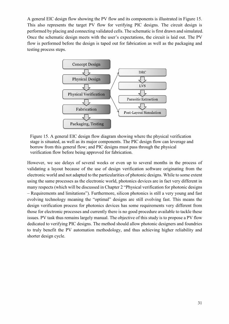
31
A general EIC design flow showing the PV flow and its components is illustrated in Figure 15. This also represents the target PV flow for verifying PIC designs. The circuit design is performed by placing and connecting validated cells. The schematic is first drawn and simulated. Once the schematic design meets with the user’s expectations, the circuit is laid out. The PV flow is performed before the design is taped out for fabrication as well as the packaging and testing process steps.
However, we see delays of several weeks or even up to several months in the process of validating a layout because of the use of design verification software originating from the electronic world and not adapted to the particularities of photonic designs. While to some extent using the same processes as the electronic world, photonics devices are in fact very different in many respects (which will be discussed in Chapter 2 “Physical verification for photonic designs – Requirements and limitations”). Furthermore, silicon photonics is still a very young and fast evolving technology meaning the “optimal” designs are still evolving fast. This means the
design verification process for photonics devices has some requirements very different from those for electronic processes and currently there is no good procedure available to tackle these issues. PV task thus remains largely manual. The objective of this study is to propose a PV flow dedicated to verifying PIC designs. The method should allow photonic designers and foundries to truly benefit the PV automation methodology, and thus achieving higher reliability and shorter design cycle.
Figure 15. A general EIC design flow diagram showing where the physical verification stage is situated, as well as its major components. The PIC design flow can leverage and borrow from this general flow; and PIC designs must pass through the physical verification flow before being approved for fabrication.
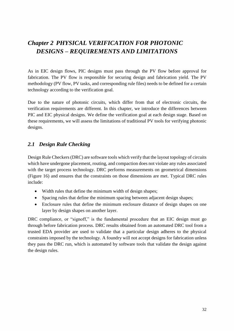
32
Chapter 2 PHYSICAL VERIFICATION FOR PHOTONIC
DESIGNS – REQUIREMENTS AND LIMITATIONS
As in EIC design flows, PIC designs must pass through the PV flow before approval for
fabrication. The PV flow is responsible for securing design and fabrication yield. The PV
methodology (PV flow, PV tasks, and corresponding rule files) needs to be defined for a certain
technology according to the verification goal.
Due to the nature of photonic circuits, which differ from that of electronic circuits, the
verification requirements are different. In this chapter, we introduce the differences between
PIC and EIC physical designs. We define the verification goal at each design stage. Based on
these requirements, we will assess the limitations of traditional PV tools for verifying photonic
designs.
2.1 Design Rule Checking
Design Rule Checkers (DRC) are software tools which verify that the layout topology of circuits
which have undergone placement, routing, and compaction does not violate any rules associated
with the target process technology. DRC performs measurements on geometrical dimensions
(Figure 16) and ensures that the constraints on those dimensions are met. Typical DRC rules
include:
Width rules that define the minimum width of design shapes;
Spacing rules that define the minimum spacing between adjacent design shapes;
Enclosure rules that define the minimum enclosure distance of design shapes on one
layer by design shapes on another layer.
DRC compliance, or “signoff,” is the fundamental procedure that an EIC design must go
through before fabrication process. DRC results obtained from an automated DRC tool from a
trusted EDA provider are used to validate that a particular design adheres to the physical
constraints imposed by the technology. A foundry will not accept designs for fabrication unless
they pass the DRC run, which is automated by software tools that validate the design against
the design rules.
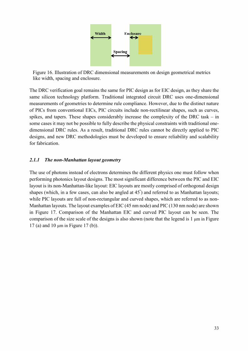
33
The DRC verification goal remains the same for PIC design as for EIC design, as they share the same silicon technology platform. Traditional integrated circuit DRC uses one-dimensional measurements of geometries to determine rule compliance. However, due to the distinct nature of PICs from conventional EICs, PIC circuits include non-rectilinear shapes, such as curves, spikes, and tapers. These shapes considerably increase the complexity of the DRC task – in some cases it may not be possible to fully describe the physical constraints with traditional one-dimensional DRC rules. As a result, traditional DRC rules cannot be directly applied to PIC designs, and new DRC methodologies must be developed to ensure reliability and scalability for fabrication.
2.1.1 The non-Manhattan layout geometry The use of photons instead of electrons determines the different physics one must follow when performing photonics layout designs. The most significant difference between the PIC and EIC layout is its non-Manhattan-like layout: EIC layouts are mostly comprised of orthogonal design shapes (which, in a few cases, can also be angled at 45º) and referred to as Manhattan layouts; while PIC layouts are full of non-rectangular and curved shapes, which are referred to as non-Manhattan layouts. The layout examples of EIC (45 nm node) and PIC (130 nm node) are shown in Figure 17. Comparison of the Manhattan EIC and curved PIC layout can be seen. The comparison of the size scale of the designs is also shown (note that the legend is 1 μm in Figure 17 (a) and 10 μm in Figure 17 (b)).
Figure 16. Illustration of DRC dimensional measurements on design geometrical metrics like width, spacing and enclosure.
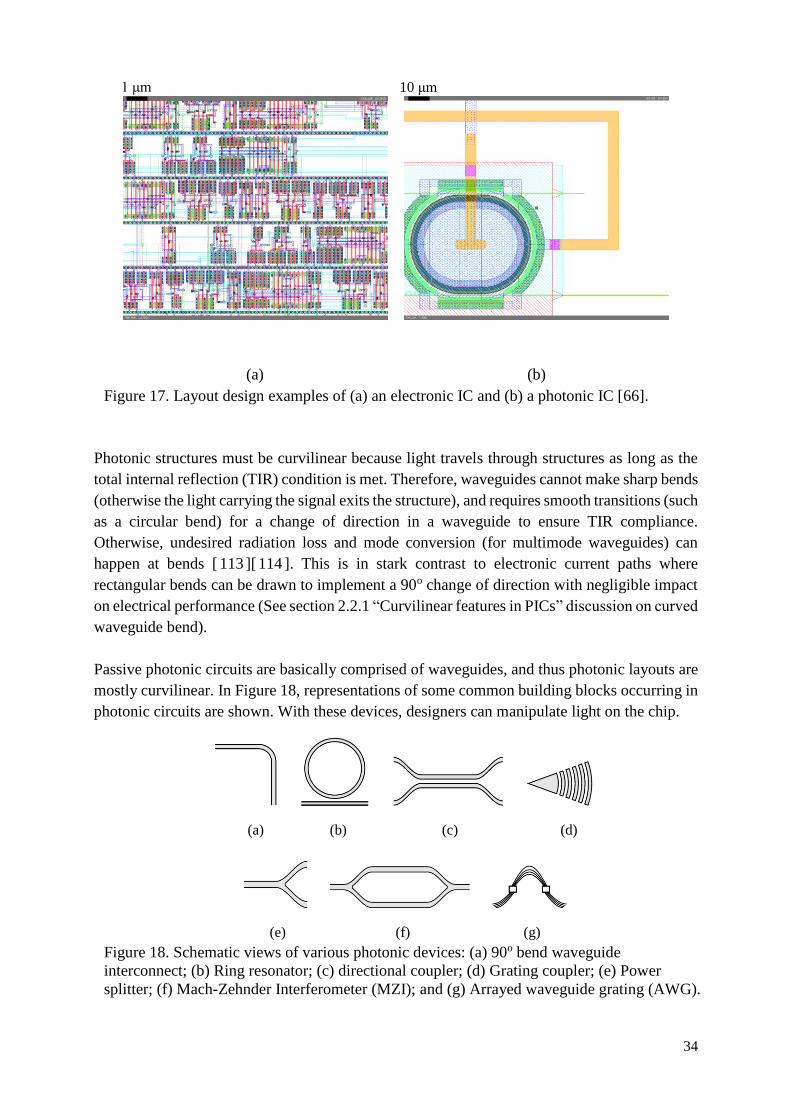
34
Photonic structures must be curvilinear because light travels through structures as long as the
total internal reflection (TIR) condition is met. Therefore, waveguides cannot make sharp bends
(otherwise the light carrying the signal exits the structure), and requires smooth transitions (such
as a circular bend) for a change of direction in a waveguide to ensure TIR compliance.
Otherwise, undesired radiation loss and mode conversion (for multimode waveguides) can
happen at bends [ 113 ][ 114 ]. This is in stark contrast to electronic current paths where
rectangular bends can be drawn to implement a 90o change of direction with negligible impact
on electrical performance (See section 2.2.1 “Curvilinear features in PICs” discussion on curved
waveguide bend).
Passive photonic circuits are basically comprised of waveguides, and thus photonic layouts are
mostly curvilinear. In Figure 18, representations of some common building blocks occurring in
photonic circuits are shown. With these devices, designers can manipulate light on the chip.
(a) (b)
Figure 17. Layout design examples of (a) an electronic IC and (b) a photonic IC [66].
(a) (b) (c) (d)
(e) (f) (g)
Figure 18. Schematic views of various photonic devices: (a) 90o bend waveguide
interconnect; (b) Ring resonator; (c) directional coupler; (d) Grating coupler; (e) Power
splitter; (f) Mach-Zehnder Interferometer (MZI); and (g) Arrayed waveguide grating (AWG).
10 μm 1 μm
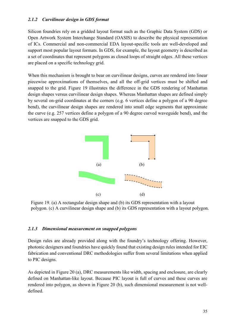
35
2.1.2 Curvilinear design in GDS format Silicon foundries rely on a gridded layout format such as the Graphic Data System (GDS) or Open Artwork System Interchange Standard (OASIS) to describe the physical representation of ICs. Commercial and non-commercial EDA layout-specific tools are well-developed and support most popular layout formats. In GDS, for example, the layout geometry is described as a set of coordinates that represent polygons as closed loops of straight edges. All these vertices are placed on a specific technology grid. When this mechanism is brought to bear on curvilinear designs, curves are rendered into linear piecewise approximations of themselves, and all the off-grid vertices must be shifted and snapped to the grid. Figure 19 illustrates the difference in the GDS rendering of Manhattan design shapes versus curvilinear design shapes. Whereas Manhattan shapes are defined simply by several on-grid coordinates at the corners (e.g. 6 vertices define a polygon of a 90 degree bend), the curvilinear design shapes are rendered into small edge segments that approximate the curve (e.g. 257 vertices define a polygon of a 90 degree curved waveguide bend), and the vertices are snapped to the GDS grid.
2.1.3 Dimensional measurement on snapped polygons Design rules are already provided along with the foundry’s technology offering. However, photonic designers and foundries have quickly found that existing design rules intended for EIC fabrication and conventional DRC methodologies suffer from several limitations when applied to PIC designs. As depicted in Figure 20 (a), DRC measurements like width, spacing and enclosure, are clearly defined on Manhattan-like layout. Because PIC layout is full of curves and these curves are rendered into polygon, as shown in Figure 20 (b), such dimensional measurement is not well-defined.
(a) (b)
(c) (d)
Figure 19. (a) A rectangular design shape and (b) its GDS representation with a layout polygon. (c) A curvilinear design shape and (b) its GDS representation with a layout polygon.
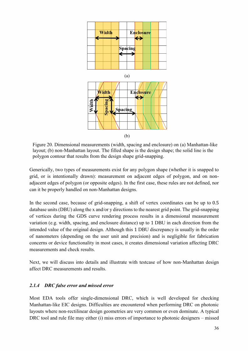
36
Generically, two types of measurements exist for any polygon shape (whether it is snapped to grid, or is intentionally drawn): measurement on adjacent edges of polygon, and on non-adjacent edges of polygon (or opposite edges). In the first case, these rules are not defined, nor can it be properly handled on non-Manhattan designs. In the second case, because of grid-snapping, a shift of vertex coordinates can be up to 0.5 database units (DBU) along the x and/or y directions to the nearest grid point. The grid-snapping of vertices during the GDS curve rendering process results in a dimensional measurement variation (e.g. width, spacing, and enclosure distance) up to 1 DBU in each direction from the intended value of the original design. Although this 1 DBU discrepancy is usually in the order of nanometers (depending on the user unit and precision) and is negligible for fabrication concerns or device functionality in most cases, it creates dimensional variation affecting DRC measurements and check results. Next, we will discuss into details and illustrate with testcase of how non-Manhattan design affect DRC measurements and results.
2.1.4 DRC false error and missed error Most EDA tools offer single-dimensional DRC, which is well developed for checking Manhattan-like EIC designs. Difficulties are encountered when performing DRC on photonic layouts where non-rectilinear design geometries are very common or even dominate. A typical DRC tool and rule file may either (i) miss errors of importance to photonic designers – missed
(a)
(b)
Figure 20. Dimensional measurements (width, spacing and enclosure) on (a) Manhattan-like layout; (b) non-Manhattan layout. The filled shape is the design shape; the solid line is the polygon contour that results from the design shape grid-snapping.
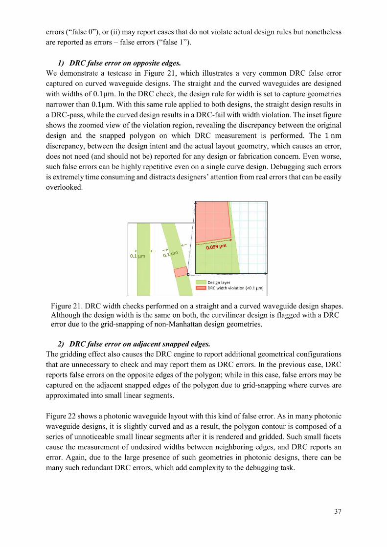
37
errors (“false 0”), or (ii) may report cases that do not violate actual design rules but nonetheless are reported as errors – false errors (“false 1”).
1) DRC false error on opposite edges. We demonstrate a testcase in Figure 21, which illustrates a very common DRC false error captured on curved waveguide designs. The straight and the curved waveguides are designed with widths of 0.1μm. In the DRC check, the design rule for width is set to capture geometries narrower than 0.1μm. With this same rule applied to both designs, the straight design results in a DRC-pass, while the curved design results in a DRC-fail with width violation. The inset figure shows the zoomed view of the violation region, revealing the discrepancy between the original design and the snapped polygon on which DRC measurement is performed. The 1 nm discrepancy, between the design intent and the actual layout geometry, which causes an error, does not need (and should not be) reported for any design or fabrication concern. Even worse, such false errors can be highly repetitive even on a single curve design. Debugging such errors is extremely time consuming and distracts designers’ attention from real errors that can be easily overlooked.
2) DRC false error on adjacent snapped edges.
The gridding effect also causes the DRC engine to report additional geometrical configurations that are unnecessary to check and may report them as DRC errors. In the previous case, DRC reports false errors on the opposite edges of the polygon; while in this case, false errors may be captured on the adjacent snapped edges of the polygon due to grid-snapping where curves are approximated into small linear segments. Figure 22 shows a photonic waveguide layout with this kind of false error. As in many photonic waveguide designs, it is slightly curved and as a result, the polygon contour is composed of a series of unnoticeable small linear segments after it is rendered and gridded. Such small facets cause the measurement of undesired widths between neighboring edges, and DRC reports an error. Again, due to the large presence of such geometries in photonic designs, there can be many such redundant DRC errors, which add complexity to the debugging task.
Figure 21. DRC width checks performed on a straight and a curved waveguide design shapes. Although the design width is the same on both, the curvilinear design is flagged with a DRC error due to the grid-snapping of non-Manhattan design geometries.
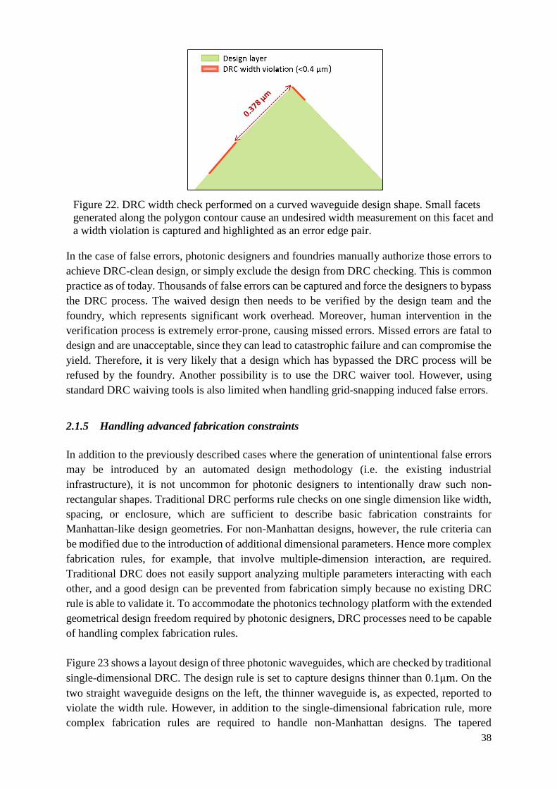
38
In the case of false errors, photonic designers and foundries manually authorize those errors to
achieve DRC-clean design, or simply exclude the design from DRC checking. This is common
practice as of today. Thousands of false errors can be captured and force the designers to bypass
the DRC process. The waived design then needs to be verified by the design team and the
foundry, which represents significant work overhead. Moreover, human intervention in the
verification process is extremely error-prone, causing missed errors. Missed errors are fatal to
design and are unacceptable, since they can lead to catastrophic failure and can compromise the
yield. Therefore, it is very likely that a design which has bypassed the DRC process will be
refused by the foundry. Another possibility is to use the DRC waiver tool. However, using
standard DRC waiving tools is also limited when handling grid-snapping induced false errors.
2.1.5 Handling advanced fabrication constraints
In addition to the previously described cases where the generation of unintentional false errors
may be introduced by an automated design methodology (i.e. the existing industrial
infrastructure), it is not uncommon for photonic designers to intentionally draw such non-
rectangular shapes. Traditional DRC performs rule checks on one single dimension like width,
spacing, or enclosure, which are sufficient to describe basic fabrication constraints for
Manhattan-like design geometries. For non-Manhattan designs, however, the rule criteria can
be modified due to the introduction of additional dimensional parameters. Hence more complex
fabrication rules, for example, that involve multiple-dimension interaction, are required.
Traditional DRC does not easily support analyzing multiple parameters interacting with each
other, and a good design can be prevented from fabrication simply because no existing DRC
rule is able to validate it. To accommodate the photonics technology platform with the extended
geometrical design freedom required by photonic designers, DRC processes need to be capable
of handling complex fabrication rules.
Figure 23 shows a layout design of three photonic waveguides, which are checked by traditional
single-dimensional DRC. The design rule is set to capture designs thinner than 0.1μm. On the
two straight waveguide designs on the left, the thinner waveguide is, as expected, reported to
violate the width rule. However, in addition to the single-dimensional fabrication rule, more
complex fabrication rules are required to handle non-Manhattan designs. The tapered
Figure 22. DRC width check performed on a curved waveguide design shape. Small facets
generated along the polygon contour cause an undesired width measurement on this facet and
a width violation is captured and highlighted as an error edge pair.
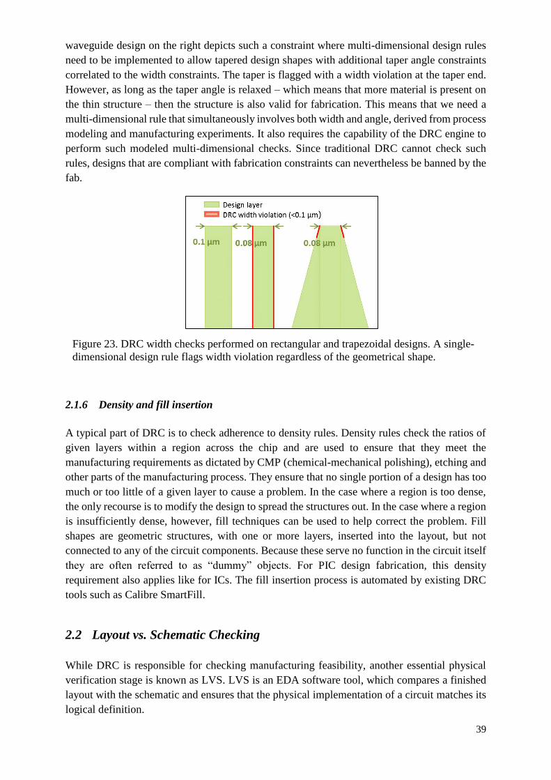
39
waveguide design on the right depicts such a constraint where multi-dimensional design rules
need to be implemented to allow tapered design shapes with additional taper angle constraints
correlated to the width constraints. The taper is flagged with a width violation at the taper end.
However, as long as the taper angle is relaxed – which means that more material is present on
the thin structure – then the structure is also valid for fabrication. This means that we need a
multi-dimensional rule that simultaneously involves both width and angle, derived from process
modeling and manufacturing experiments. It also requires the capability of the DRC engine to
perform such modeled multi-dimensional checks. Since traditional DRC cannot check such
rules, designs that are compliant with fabrication constraints can nevertheless be banned by the
fab.
2.1.6 Density and fill insertion
A typical part of DRC is to check adherence to density rules. Density rules check the ratios of
given layers within a region across the chip and are used to ensure that they meet the
manufacturing requirements as dictated by CMP (chemical-mechanical polishing), etching and
other parts of the manufacturing process. They ensure that no single portion of a design has too
much or too little of a given layer to cause a problem. In the case where a region is too dense,
the only recourse is to modify the design to spread the structures out. In the case where a region
is insufficiently dense, however, fill techniques can be used to help correct the problem. Fill
shapes are geometric structures, with one or more layers, inserted into the layout, but not
connected to any of the circuit components. Because these serve no function in the circuit itself
they are often referred to as “dummy” objects. For PIC design fabrication, this density
requirement also applies like for ICs. The fill insertion process is automated by existing DRC
tools such as Calibre SmartFill.
2.2 Layout vs. Schematic Checking
While DRC is responsible for checking manufacturing feasibility, another essential physical
verification stage is known as LVS. LVS is an EDA software tool, which compares a finished
layout with the schematic and ensures that the physical implementation of a circuit matches its
logical definition.
Figure 23. DRC width checks performed on rectangular and trapezoidal designs. A single-
dimensional design rule flags width violation regardless of the geometrical shape.
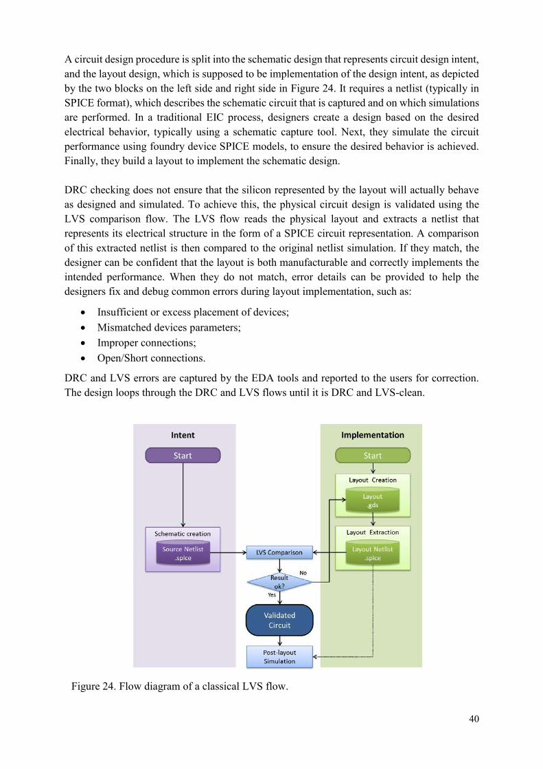
40
A circuit design procedure is split into the schematic design that represents circuit design intent, and the layout design, which is supposed to be implementation of the design intent, as depicted by the two blocks on the left side and right side in Figure 24. It requires a netlist (typically in SPICE format), which describes the schematic circuit that is captured and on which simulations are performed. In a traditional EIC process, designers create a design based on the desired electrical behavior, typically using a schematic capture tool. Next, they simulate the circuit performance using foundry device SPICE models, to ensure the desired behavior is achieved. Finally, they build a layout to implement the schematic design. DRC checking does not ensure that the silicon represented by the layout will actually behave as designed and simulated. To achieve this, the physical circuit design is validated using the LVS comparison flow. The LVS flow reads the physical layout and extracts a netlist that represents its electrical structure in the form of a SPICE circuit representation. A comparison of this extracted netlist is then compared to the original netlist simulation. If they match, the designer can be confident that the layout is both manufacturable and correctly implements the intended performance. When they do not match, error details can be provided to help the designers fix and debug common errors during layout implementation, such as:
Insufficient or excess placement of devices; Mismatched devices parameters; Improper connections; Open/Short connections.
DRC and LVS errors are captured by the EDA tools and reported to the users for correction. The design loops through the DRC and LVS flows until it is DRC and LVS-clean.
Figure 24. Flow diagram of a classical LVS flow.
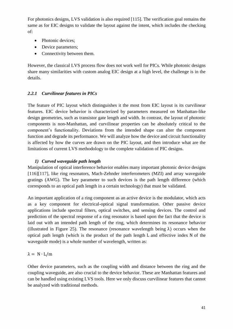
41
For photonics designs, LVS validation is also required [115]. The verification goal remains the
same as for EIC designs to validate the layout against the intent, which includes the checking
of:
Photonic devices;
Device parameters;
Connectivity between them.
However, the classical LVS process flow does not work well for PICs. While photonic designs
share many similarities with custom analog EIC design at a high level, the challenge is in the
details.
2.2.1 Curvilinear features in PICs
The feature of PIC layout which distinguishes it the most from EIC layout is its curvilinear
features. EIC device behavior is characterized by parameters measured on Manhattan-like
design geometries, such as transistor gate length and width. In contrast, the layout of photonic
components is non-Manhattan, and curvilinear properties can be absolutely critical to the
component’s functionality. Deviations from the intended shape can alter the component
function and degrade its performance. We will analyze how the device and circuit functionality
is affected by how the curves are drawn on the PIC layout, and then introduce what are the
limitations of current LVS methodology to the complete validation of PIC designs.
1) Curved waveguide path length
Manipulation of optical interference behavior enables many important photonic device designs
[116][117], like ring resonators, Mach-Zehnder interferometers (MZI) and array waveguide
gratings (AWG). The key parameter to such devices is the path length difference (which
corresponds to an optical path length in a certain technology) that must be validated.
An important application of a ring component as an active device is the modulator, which acts
as a key component for electrical-optical signal transformation. Other passive device
applications include spectral filters, optical switches, and sensing devices. The control and
prediction of the spectral response of a ring resonator is based upon the fact that the device is
laid out with an intended path length of the ring, which determines its resonance behavior
(illustrated in Figure 25). The resonance (resonance wavelength being λ) occurs when the
optical path length (which is the product of the path length L and effective index N of the
waveguide mode) is a whole number of wavelength, written as:
λ = N ∙ L/m
Other device parameters, such as the coupling width and distance between the ring and the
coupling waveguide, are also crucial to the device behavior. These are Manhattan features and
can be handled using existing LVS tools. Here we only discuss curvilinear features that cannot
be analyzed with traditional methods.
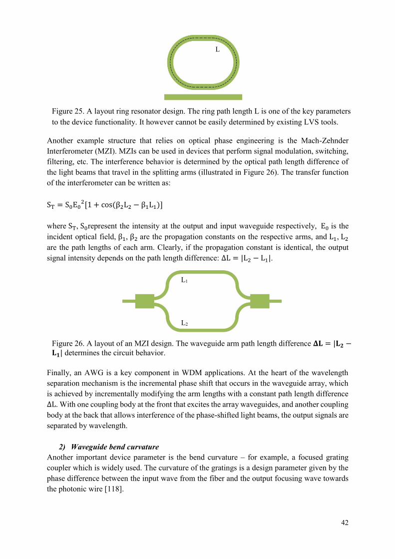
42
Another example structure that relies on optical phase engineering is the Mach-Zehnder Interferometer (MZI). MZIs can be used in devices that perform signal modulation, switching, filtering, etc. The interference behavior is determined by the optical path length difference of the light beams that travel in the splitting arms (illustrated in Figure 26). The transfer function of the interferometer can be written as: ST = S0E0
2[1 + cos(β2L2 − β1L1)] where ST, S0represent the intensity at the output and input waveguide respectively, E0 is the incident optical field, β1, β2 are the propagation constants on the respective arms, and L1, L2 are the path lengths of each arm. Clearly, if the propagation constant is identical, the output signal intensity depends on the path length difference: ΔL = |L2 − L1|.
Finally, an AWG is a key component in WDM applications. At the heart of the wavelength separation mechanism is the incremental phase shift that occurs in the waveguide array, which is achieved by incrementally modifying the arm lengths with a constant path length difference ΔL. With one coupling body at the front that excites the array waveguides, and another coupling body at the back that allows interference of the phase-shifted light beams, the output signals are separated by wavelength.
2) Waveguide bend curvature Another important device parameter is the bend curvature – for example, a focused grating coupler which is widely used. The curvature of the gratings is a design parameter given by the phase difference between the input wave from the fiber and the output focusing wave towards the photonic wire [118].
Figure 25. A layout ring resonator design. The ring path length L is one of the key parameters to the device functionality. It however cannot be easily determined by existing LVS tools.
Figure 26. A layout of an MZI design. The waveguide arm path length difference 𝚫𝐋 = |𝐋𝟐 −𝐋𝟏| determines the circuit behavior.
L
L1
L2
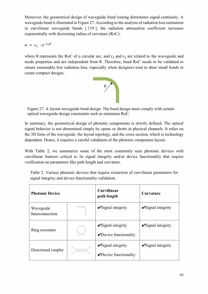
43
Moreover, the geometrical design of waveguide bend routing determines signal continuity. A waveguide bend is illustrated in Figure 27. According to the analysis of radiation loss estimation in curvilinear waveguide bends [ 119 ], the radiation attenuation coefficient increases exponentially with decreasing radius of curvature (RoC): α = c1 ∙ e−c2𝑅 where R represents the RoC of a circular arc, and c1 and c2 are related to the waveguide and mode properties and are independent from R. Therefore, bend RoC needs to be validated to ensure reasonably low radiation loss, especially when designers tend to draw small bends to create compact designs.
In summary, the geometrical design of photonic components is strictly defined. The optical signal behavior is not determined simply by opens or shorts in physical channels. It relies on the 3D form of the waveguide: the layout topology, and the cross-section, which is technology dependent. Hence, it requires a careful validation of the photonic component layout. With Table 2, we summarize some of the most commonly seen photonic devices with curvilinear features critical to its signal integrity and/or device functionality that require verification on parameters like path length and curvature.
Photonic Device Curvilinear path length Curvature
Waveguide Interconnection
✔ Signal integrity ✔ Signal integrity
Ring resonator
✔ Signal integrity
✔ Device functionality
✔ Signal integrity
Directional coupler
✔ Signal integrity
✔ Device functionality
✔ Signal integrity
Figure 27. A layout waveguide bend design. The bend design must comply with certain optical waveguide design constraints such as minimum RoC.
Table 2. Various photonic devices that require extraction of curvilinear parameters for signal integrity and device functionality validation.
R
44
Focused grating coupler
✔ Device functionality
Y-junction splitter
✔ Signal integrity
✔ Signal integrity
Mach-Zehnder interferometer (MZI)
✔ Signal integrity
✔ Device functionality
✔ Signal integrity
Array waveguide grating (AWG)
✔ Signal integrity
✔ Device functionality
✔ Signal integrity
2.2.2 Handling curvilinear data in standard layout format As discussed in section 2.1 “Design Rule Checking”, current commercial EDA tools are well-suited for Manhattan layouts; and the current layout format accepted by fabs are raster image data like GDS, in which the layout geometries are stored as a series of discrete coordinates. This being said, they do not support an appropriate curve representation methodology, nor any curve parameter extraction capability, for verifying curvilinear designs. In this context, we need to handle curvilinear design shape and photonic device curvilinear properties based on the discrete layout database.
2.2.3 Representation of photonic device feature in standard netlist format As introduced in the beginning, a netlist file is used to store source and extracted circuit descriptions. When matching the two netlists, both device parameters as well as circuit topology are compared. For EIC designs, a SPICE netlist is a commonly used netlist format for analog integrated circuit simulation tools. A MOSFET transistor, for example, is represented as followed:
where M1 is the name of the specific transistor instance; Drain, Gate, Source, Bulk denote the transistor’s drain, gate, source and bulk nodes respectively; NMOS specifies the device model being the built-in N-type MOSFET; and W and L are the width and length properties ("u" indicates a micro, or 10-6, dimension multiplier) of the NMOS transistor. This property set is sufficient to describe Manhattan-like EIC designs. It is also possible to describe a simple curvilinear device, such as a regular 90° circular bend waveguide (model WG_BEND) with its width (W), length (L), bend radius (R) properties written as (for example):
M1 Drain Gate Source Bulk NMOS W = 0.25u L = 0.25u
45
Here, the radial bend can be characterized with a unique RoC value R. However, the syntax is
severely limited when trying to describe more complex devices with critical curvilinear
properties. In the case of a design with non-unique RoC along the curve for example, like a
spline bend [120] or a sinusoidal bend [121], it cannot be represented easily with a set of
parameters stored in the described way.
2.2.4 Representation of waveguide interconnect in standard netlist format
In the EIC world, extraction and comparison of the circuit is not sufficient to ensure that the
circuit will meet the intended behavior. This is because metal interconnects have resistive and
capacitive impacts (termed "parasitics") on the circuit. In traditional LVS, these interconnects
are treated as ‘ideal’. There is nothing to compare them to as there is no place in the historic
SPICE format to hold the parameters. As such, the parasitic extraction flow is used to
characterize the interconnects to identify and insert them into an extracted netlist where these
parasitic resistors or capacitors may reside. This extracted netlist can then be used in subsequent
simulations (post-layout simulation step) to validate whether their impact has invalidated the
design behavior beyond expectation.
While the transport mechanisms in the optics world are very different to those in the electronics
world, there may be an equivalent to the parasitic extraction flow for photonics. If a photonic
layout is generated using traditional EDA tools, it is likely that the waveguide interconnects are
also not considered as devices when passing to simulation. The waveguides will therefore need
to be extracted and passed to get the most accurate post-layout simulation results, as discussed
in section 2.1.4 “Curvilinear features in PICs”. In some practices, photonic designers may prefer
to build strictly from the layout, forgoing any schematic capture from the start. In this situation,
post-layout simulations can rely only on what is extracted out. Of course, this makes debugging
of shorts and opens dependent on simulation results only, increasing debug time.
2.2.5 Photonic device and connectivity definition
The typical LVS flow goes through three stages: recognition of the devices in the layout,
characterization of the devices, and comparison of the device connectivity and parameters with
those in the schematics.
The device is the basic component with its ports (as pins when it is placed into the circuit) and
simulation model that can be placed and connected into the circuit. Most LVS tools are
developed under the assumption that an analysis of the layout can rely on logic properties of
individual CMOS gates described in widely available libraries. The basic elements of a photonic
circuit, such as resonators, modulators and multiplexers, are quite different. Until silicon
photonics reaches greater maturity, it is unlikely that common LVS tools will support all the
basic photonic devices as "native devices" at the same level as they support MOSFETs and
CMOS gates. Instead, the LVS tool must support user-defined devices and circuit patterns.
B1 Optical_in Optical_out WG_BEND W=0.5u L=7.85u R=5u
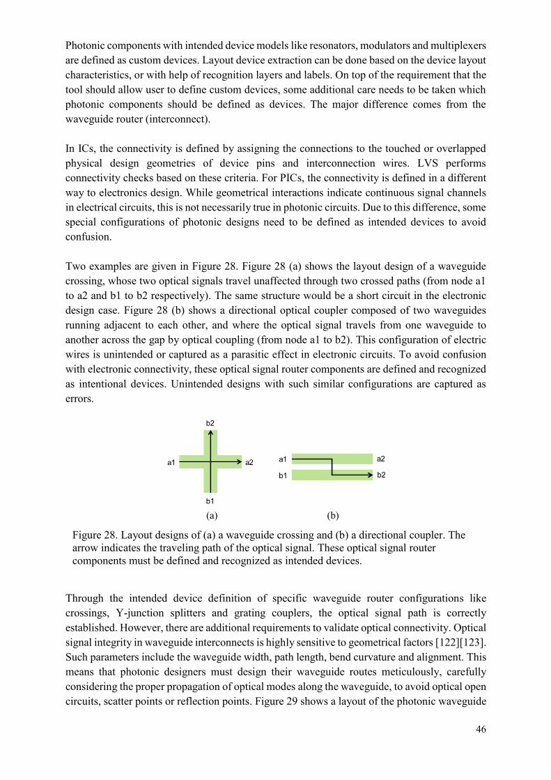
46
Photonic components with intended device models like resonators, modulators and multiplexers are defined as custom devices. Layout device extraction can be done based on the device layout characteristics, or with help of recognition layers and labels. On top of the requirement that the tool should allow user to define custom devices, some additional care needs to be taken which photonic components should be defined as devices. The major difference comes from the waveguide router (interconnect). In ICs, the connectivity is defined by assigning the connections to the touched or overlapped physical design geometries of device pins and interconnection wires. LVS performs connectivity checks based on these criteria. For PICs, the connectivity is defined in a different way to electronics design. While geometrical interactions indicate continuous signal channels in electrical circuits, this is not necessarily true in photonic circuits. Due to this difference, some special configurations of photonic designs need to be defined as intended devices to avoid confusion. Two examples are given in Figure 28. Figure 28 (a) shows the layout design of a waveguide crossing, whose two optical signals travel unaffected through two crossed paths (from node a1 to a2 and b1 to b2 respectively). The same structure would be a short circuit in the electronic design case. Figure 28 (b) shows a directional optical coupler composed of two waveguides running adjacent to each other, and where the optical signal travels from one waveguide to another across the gap by optical coupling (from node a1 to b2). This configuration of electric wires is unintended or captured as a parasitic effect in electronic circuits. To avoid confusion with electronic connectivity, these optical signal router components are defined and recognized as intentional devices. Unintended designs with such similar configurations are captured as errors.
Through the intended device definition of specific waveguide router configurations like crossings, Y-junction splitters and grating couplers, the optical signal path is correctly established. However, there are additional requirements to validate optical connectivity. Optical signal integrity in waveguide interconnects is highly sensitive to geometrical factors [122][123]. Such parameters include the waveguide width, path length, bend curvature and alignment. This means that photonic designers must design their waveguide routes meticulously, carefully considering the proper propagation of optical modes along the waveguide, to avoid optical open circuits, scatter points or reflection points. Figure 29 shows a layout of the photonic waveguide
(a) (b)
Figure 28. Layout designs of (a) a waveguide crossing and (b) a directional coupler. The arrow indicates the traveling path of the optical signal. These optical signal router components must be defined and recognized as intended devices.
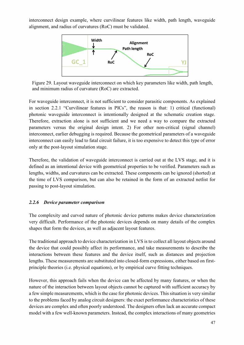
47
interconnect design example, where curvilinear features like width, path length, waveguide alignment, and radius of curvatures (RoC) must be validated.
For waveguide interconnect, it is not sufficient to consider parasitic components. As explained in section 2.2.1 “Curvilinear features in PICs”, the reason is that: 1) critical (functional) photonic waveguide interconnect is intentionally designed at the schematic creation stage. Therefore, extraction alone is not sufficient and we need a way to compare the extracted parameters versus the original design intent. 2) For other non-critical (signal channel) interconnect, earlier debugging is required. Because the geometrical parameters of a waveguide interconnect can easily lead to fatal circuit failure, it is too expensive to detect this type of error only at the post-layout simulation stage. Therefore, the validation of waveguide interconnect is carried out at the LVS stage, and it is defined as an intentional device with geometrical properties to be verified. Parameters such as lengths, widths, and curvatures can be extracted. These components can be ignored (shorted) at the time of LVS comparison, but can also be retained in the form of an extracted netlist for passing to post-layout simulation.
2.2.6 Device parameter comparison The complexity and curved nature of photonic device patterns makes device characterization very difficult. Performance of the photonic devices depends on many details of the complex shapes that form the devices, as well as adjacent layout features. The traditional approach to device characterization in LVS is to collect all layout objects around the device that could possibly affect its performance, and take measurements to describe the interactions between these features and the device itself, such as distances and projection lengths. These measurements are substituted into closed-form expressions, either based on first-principle theories (i.e. physical equations), or by empirical curve fitting techniques. However, this approach fails when the device can be affected by many features, or when the nature of the interaction between layout objects cannot be captured with sufficient accuracy by a few simple measurements, which is the case for photonic devices. This situation is very similar to the problems faced by analog circuit designers: the exact performance characteristics of these devices are complex and often poorly understood. The designers often lack an accurate compact model with a few well-known parameters. Instead, the complex interactions of many geometries
Figure 29. Layout waveguide interconnect on which key parameters like width, path length, and minimum radius of curvature (RoC) are extracted.
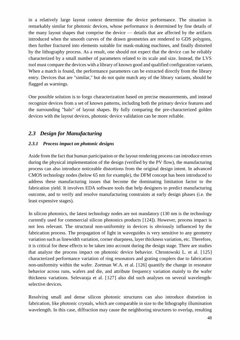
48
in a relatively large layout context determine the device performance. The situation is
remarkably similar for photonic devices, whose performance is determined by fine details of
the many layout shapes that comprise the device — details that are affected by the artifacts
introduced when the smooth curves of the drawn geometries are rendered to GDS polygons,
then further fractured into elements suitable for mask-making machines, and finally distorted
by the lithography process. As a result, one should not expect that the device can be reliably
characterized by a small number of parameters related to its scale and size. Instead, the LVS
tool must compare the devices with a library of known good and qualified configuration variants.
When a match is found, the performance parameters can be extracted directly from the library
entry. Devices that are "similar," but do not quite match any of the library variants, should be
flagged as warnings.
One possible solution is to forgo characterization based on precise measurements, and instead
recognize devices from a set of known patterns, including both the primary device features and
the surrounding "halo" of layout shapes. By fully comparing the pre-characterized golden
devices with the layout devices, photonic device validation can be more reliable.
2.3 Design for Manufacturing
2.3.1 Process impact on photonic designs
Aside from the fact that human participation or the layout rendering process can introduce errors
during the physical implementation of the design (verified by the PV flow), the manufacturing
process can also introduce noticeable distortions from the original design intent. In advanced
CMOS technology nodes (below 65 nm for example), the DFM concept has been introduced to
address these manufacturing issues that become the dominating limitation factor to the
fabrication yield. It involves EDA software tools that help designers to predict manufacturing
outcome, and to verify and resolve manufacturing constraints at early design phases (i.e. the
least expensive stages).
In silicon photonics, the latest technology nodes are not mandatory (130 nm is the technology
currently used for commercial silicon photonics products [124]). However, process impact is
not less relevant. The structural non-uniformity in devices is obviously influenced by the
fabrication process. The propagation of light in waveguides is very sensitive to any geometry
variation such as linewidth variation, corner sharpness, layer thickness variation, etc. Therefore,
it is critical for these effects to be taken into account during the design stage. There are studies
that analyze the process impact on photonic device behavior. Chrostowski L. et al. [125]
characterized performance variation of ring resonators and grating couplers due to fabrication
non-uniformity within the wafer. Zortman W.A. et al. [126] quantify the change in resonator
behavior across runs, wafers and die, and attribute frequency variation mainly to the wafer
thickness variations. Selevaraja et al. [127] also did such analyses on several wavelength-
selective devices.
Resolving small and dense silicon photonic structures can also introduce distortion in
fabrication, like photonic crystals, which are comparable in size to the lithography illumination
wavelength. In this case, diffraction may cause the neighboring structures to overlap, resulting
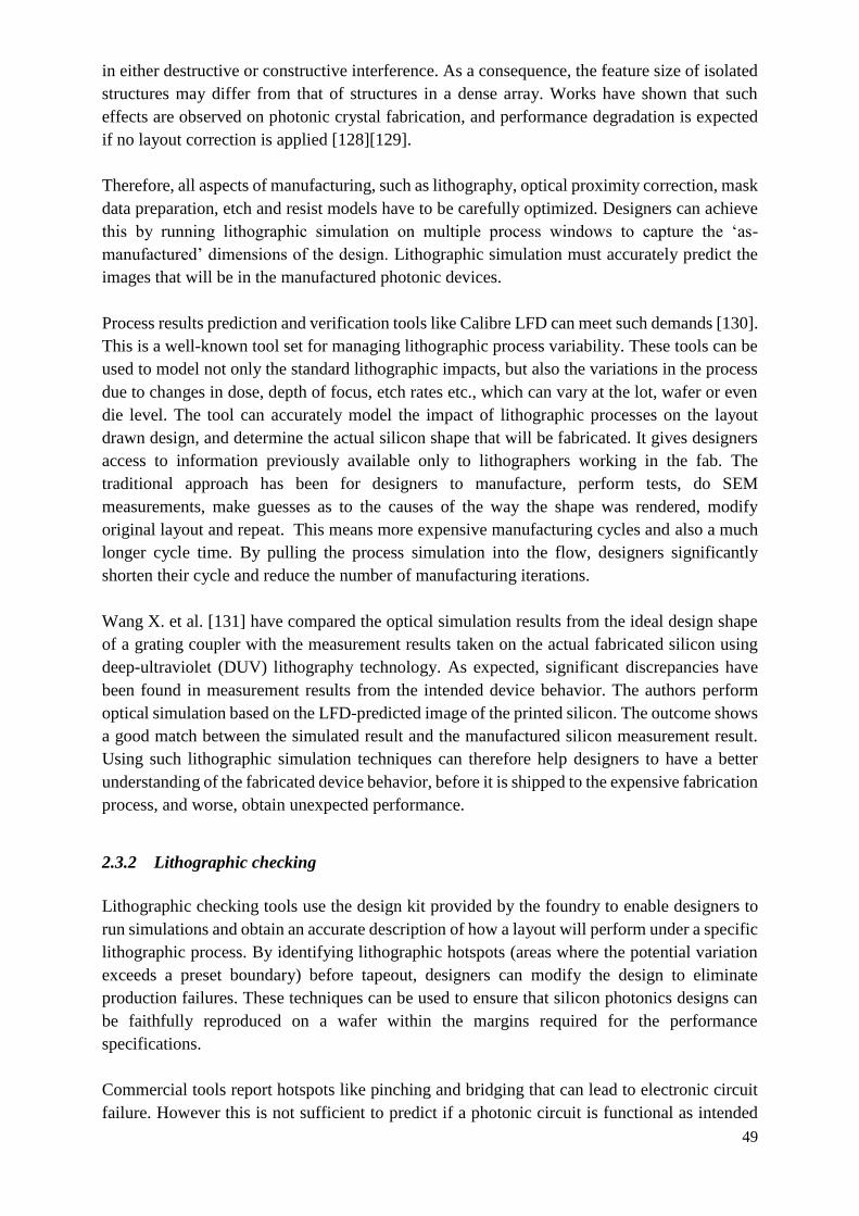
49
in either destructive or constructive interference. As a consequence, the feature size of isolated
structures may differ from that of structures in a dense array. Works have shown that such
effects are observed on photonic crystal fabrication, and performance degradation is expected
if no layout correction is applied [128][129].
Therefore, all aspects of manufacturing, such as lithography, optical proximity correction, mask
data preparation, etch and resist models have to be carefully optimized. Designers can achieve
this by running lithographic simulation on multiple process windows to capture the ‘as-
manufactured’ dimensions of the design. Lithographic simulation must accurately predict the
images that will be in the manufactured photonic devices.
Process results prediction and verification tools like Calibre LFD can meet such demands [130].
This is a well-known tool set for managing lithographic process variability. These tools can be
used to model not only the standard lithographic impacts, but also the variations in the process
due to changes in dose, depth of focus, etch rates etc., which can vary at the lot, wafer or even
die level. The tool can accurately model the impact of lithographic processes on the layout
drawn design, and determine the actual silicon shape that will be fabricated. It gives designers
access to information previously available only to lithographers working in the fab. The
traditional approach has been for designers to manufacture, perform tests, do SEM
measurements, make guesses as to the causes of the way the shape was rendered, modify
original layout and repeat. This means more expensive manufacturing cycles and also a much
longer cycle time. By pulling the process simulation into the flow, designers significantly
shorten their cycle and reduce the number of manufacturing iterations.
Wang X. et al. [131] have compared the optical simulation results from the ideal design shape
of a grating coupler with the measurement results taken on the actual fabricated silicon using
deep-ultraviolet (DUV) lithography technology. As expected, significant discrepancies have
been found in measurement results from the intended device behavior. The authors perform
optical simulation based on the LFD-predicted image of the printed silicon. The outcome shows
a good match between the simulated result and the manufactured silicon measurement result.
Using such lithographic simulation techniques can therefore help designers to have a better
understanding of the fabricated device behavior, before it is shipped to the expensive fabrication
process, and worse, obtain unexpected performance.
2.3.2 Lithographic checking
Lithographic checking tools use the design kit provided by the foundry to enable designers to
run simulations and obtain an accurate description of how a layout will perform under a specific
lithographic process. By identifying lithographic hotspots (areas where the potential variation
exceeds a preset boundary) before tapeout, designers can modify the design to eliminate
production failures. These techniques can be used to ensure that silicon photonics designs can
be faithfully reproduced on a wafer within the margins required for the performance
specifications.
Commercial tools report hotspots like pinching and bridging that can lead to electronic circuit
failure. However this is not sufficient to predict if a photonic circuit is functional as intended

50
after manufacturing, due to the fact that photonic device behavior is determined by more details
in geometry. Photonic design hotspot detection should be able to compare the ‘as manufactured’
simulation results with the original intended device and determine if the device geometrical
dimensions are within requirements, and if the manufacturing variance is within an acceptable
range. Addressing these issues during design allows for correction before manufacturing.
2.4 Considerations on Post-Layout Flow
The post-tapeout flow is not within the scope of this study. However, it involves crucial steps
that allow silicon photonic design to be sent for fabrication, and some of these aspects need to
be taken into consideration at prior design stages. So we will briefly introduce the main post-
tapeout steps and the challenges as suggestions for future area of exploration.
A post-tapeout flow is mainly comprised of following components:
OPC (Optical Proximity Correction)
LRC (Litho Rule Check) or LPC (Litho Print Check)
MDP (Mask Data Preparation)
MRC (Mask Rule Check)
At this stage, the foundry obtains the layout input from designers or design houses (in GDSII
or OASIS format), and it is usually the foundry’s responsibility to correct, verify and transform
the layout into the appropriate data for photomask fabrication. The main difference between
PIC and EIC layouts is the presence of abundant non-Manhattan features. As with conventional
physical verification tools, post-layout tools are not designed to handle non-Manhattan features.
Adding to the complexity is the sensitivity of photonic device behavior to its geometrical
topology, which requires the data manipulation process to retain as much original information
as possible.
1) OPC (Optical Proximity Correction)
While it is useful to visualize geometric differences between layout and manufacturing, as is
capturing behavioral simulation differences (as discussed in section 2.3.2 Lithographic
checking), this does not help the designer to know what to do in the case when the circuit layout
does not meet the desired behavior. Some methods to determine the structures and suggest or
even automate changes to the layout that can result in the intended designed representation in
the manufactured structure are required. In the EIC world this is often referred to as retargeting.
Retargeting generally takes the form of adding or subtracting small shapes at the corners of a
Manhattan wire or device shape. By creating these shapes, known as serifs, of a size too small
to manufacture, their presence (or removal) can pull the lithographic optical imaging of those
shapes to more closely meet the original design. This retargeting may be done by the foundry,
or in some cases by the designer if required for accurate simulation.
In the work of Bogaerts W. et al. [132], they showed device performance differences given by
the simulation results on the original design and on the OPC corrected design. An example of
the actual fabricated silicon image of a Bragg grating device is shown in Figure 30, of which
the contour is corrugated compared to the original layout design. Figure 31 (a) and (b) show the
51
ideal layout design of the Bragg grating as well as its corrected layout after an OPC correction.
The measured performance results of the corrected and uncorrected device are demonstrated in
[131].
The benefit of performing OPC on photonic layout can be clearly observed. The closer the
printed silicon image is to the original intended design shape, the closer is the fabricated device
performance to that of the intent. While this approach may help for Manhattan design structures
such as the Bragg grating example, it does not lend itself easily to the curved shapes in typical
photonics circuits. A new retargeting method is required. Early results research suggests that
modifying a curve or skew edge to be comprised of small stair-steps, may work to keep the
original integrity of the intended shape. However, the modified staircase-like layout risks
degrading device performance. There are layout image processing tools based on pixels instead
of edge fragments, like Calibre pxOPC, which can be exploited for implementations on curved
layouts like silicon photonics.
2) MDP (Mask Data Preparation)
MDP is the procedure of translating a file containing the intended set of polygons from a layout
into a set of instructions that a photomask writer can use to generate a physical mask. MDP
involves mask fracturing, where complex polygons are translated into simpler shapes, often
rectangles and trapezoids that can be handled by the mask writing hardware.
Mask discretization also has a very large impact on the performance characteristics of photonic
devices. Research reports that mask discretization can introduce significant degradation in
device performance, like AWGs [133][134]. When creating non-Manhattan geometries for
Figure 30. The fabricated silicon image of a bragg grating device. The dotted line is the
mask layout contour. [132]
(a)
(b)
Figure 31. (a) A design layout of Bragg gratings. (b) The retargeted layout of the design.
The printed silicon image is closer to the original design intent with such processing.
52
photonic designs, it approximates the design using abutted rectangular shots or small shapes to
smooth out line edge roughness. To remain faithful to the original pattern, this approach results
in unacceptably large volumes of mask data, thus leading to increased mask cost and processing
runtime. There are studies dedicated to mask writing time optimization for non-Manhattan
designs, such as algorithms for optimizing mask fracturing combined with e-beam writer
modifications [135]. In the future, as silicon photonic devices share more and more silicon area
with conventional CMOS devices, a radically different approach may be required. The state-of-
the-art computational geometry library, Computational Geometry Algorithms Library (CGAL),
supports curves for the construction of arrangements and 2-D intersection of curves [136], but
performance is not comparable to standard scan line implementations. Recent advances in
processing parameterized curves are needed for an effective solution.
3) LRC (Litho Rule Check) and MRC (Mask Rule Check)
While DRC is used to verify the manufacturability of the design layout, MRC is used to perform
similar verifications, like dimensional checking on width, spacing and enclosure. MRC is
responsible for checking the mask data processed by MDP. The MDP process contains many
types of data conversion and modification such as fracturing, rotation, mirroring, sizing and job
deck arrangement. During this data conversion, there is a possibility that some errors might be
generated and a photomask might be manufactured with erroneous data. Therefore, the MRC
step is essential, in addition to DRC. Similar challenges are met in MRC as in DRC, originating
in the non-Manhattan design geometries of photonic designs (as introduced in section 2.1
Design Rule Checking).
LRC also performs geometrical measurements and checks like DRC or MRC, while its target
is the predicted silicon image given by the lithographic simulation. Violations like pinching and
bridging due to lithographic limitations can be found by LRC. As discussed in section 2.3.2
Lithographic checking, photonic design imposes different checking requirements: for example,
CD variation and corner rounding can be critical to photonic device behavior.
In summary, the post-layout flow is handled separately by the foundry, and they report to
upstream designers any failures detected during OPC, LRC, MDP, or MRC steps. For photonic
layout, the most common failures are related to processing non-Manhattan geometries, which
can lead to huge volumes of mask data, and possible deviations of mask shapes from the original
design intent. This introduces the demand for designer awareness of mask data at early design
phases [137]. As introduced in section 2.3 Design for Manufacturing, incorporating process
variation effects at design and physical verification stages can shorten the silicon photonics
design cycle. The same could be true for mask data preparation. Considering downstream
photomask manufacturing effects at the design stage can potentially help control photomask
costs and cycle time while ensuring the emphasis is placed on addressing performance issues.
Currently, such a mechanism does not yet exist. Designers are only aware of post-layout
constraints when the post-layout team informs them of any issues occurred (which is very often
in the case of photonic design ). This remains a future area of study.

53
Chapter 3 DESIGN RULE CHECKING (DRC)
Design rules are a set of rules that restrict the parameters of layout design geometries. These
rules are set to allow designers to exploit full fabrication capability while avoiding potential
fabrication failure. Design rules are specific to a particular technology and are prescribed by the
foundry or fabrication facility. Adherence to design rules helps ensure acceptable yield of the
layout designs. The DRC methodology is well-established in EIC designs. With the automated
flow, any design feature that is non-compliant with the design rules is captured and is reported
for correction.
However, as analyzed in Chapter 2 “PV for Photonic Designs–Requirements and Limitations”,
the presence of all-angle and curvilinear design shapes causes difficulties and incapability of
the classical tool when handling photonic layout. In this chapter, we will propose solutions to
address these challenges.
3.1 Solutions to DRC on Non-Manhattan Designs
To adapt to the complex geometrical design of photonic circuits, we need real-world design
rules and more sophisticated DRC tools to handle such design rules. Here, we take advantage
of a programmable modeling engine interfaced with traditional DRC, known as equation-based
DRC (Calibre eqDRC). It extends the capability of traditional DRC that enables users to analyze
complex, multi-dimensional interactions that are difficult or impossible to verify using
traditional DRC methods. Its development was originally motivated by the EIC physical
verification difficulty at advanced technology nodes [138][139], but eqDRC is equally adept at
resolving photonic layout geometrical verification requirements. It helps to filter false errors by
applying proper filtering conditions that can be composed of various geometrical measurements,
mathematical operations, and conditions. False errors are thus effectively suppressed. We
explore and propose filtering criteria to distinguish snapped geometries from Manhattan ones,
and we compare the results by applying traditional DRC and eqDRC respectively. The
interaction of multiple dimensional parameters can be modeled by a mathematical function and
transformed into a single rule check. As a result, greater geometrical design freedom is
permitted, and at the same time, yield is ensured by a more accurate description of the
manufacturing rules.
3.1.1 Conditional DRC result post-filtering
A quick workaround to avoid gridding-induced false errors is to relax dimensional check
constraints by applying a DRC tolerance factor. Juneidi et al. [140] presented a method to solve
some similar DRC problems on microelectromechanical system (MEMS) designs, which also
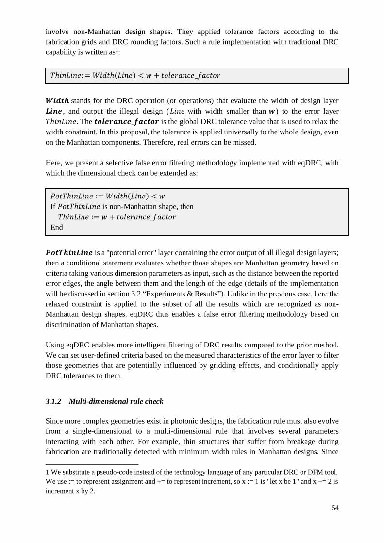
54
involve non-Manhattan design shapes. They applied tolerance factors according to the
fabrication grids and DRC rounding factors. Such a rule implementation with traditional DRC
capability is written as1:
𝑾𝒊𝒅𝒕𝒉 stands for the DRC operation (or operations) that evaluate the width of design layer
𝑳𝒊𝒏𝒆 , and output the illegal design (𝐿𝑖𝑛𝑒 with width smaller than 𝒘 ) to the error layer
𝑇ℎ𝑖𝑛𝐿𝑖𝑛𝑒. The 𝒕𝒐𝒍𝒆𝒓𝒂𝒏𝒄𝒆_𝒇𝒂𝒄𝒕𝒐𝒓 is the global DRC tolerance value that is used to relax the
width constraint. In this proposal, the tolerance is applied universally to the whole design, even
on the Manhattan components. Therefore, real errors can be missed.
Here, we present a selective false error filtering methodology implemented with eqDRC, with
which the dimensional check can be extended as:
𝑷𝒐𝒕𝑻𝒉𝒊𝒏𝑳𝒊𝒏𝒆 is a "potential error" layer containing the error output of all illegal design layers;
then a conditional statement evaluates whether those shapes are Manhattan geometry based on
criteria taking various dimension parameters as input, such as the distance between the reported
error edges, the angle between them and the length of the edge (details of the implementation
will be discussed in section 3.2 “Experiments & Results”). Unlike in the previous case, here the
relaxed constraint is applied to the subset of all the results which are recognized as non-
Manhattan design shapes. eqDRC thus enables a false error filtering methodology based on
discrimination of Manhattan shapes.
Using eqDRC enables more intelligent filtering of DRC results compared to the prior method.
We can set user-defined criteria based on the measured characteristics of the error layer to filter
those geometries that are potentially influenced by gridding effects, and conditionally apply
DRC tolerances to them.
3.1.2 Multi-dimensional rule check
Since more complex geometries exist in photonic designs, the fabrication rule must also evolve
from a single-dimensional to a multi-dimensional rule that involves several parameters
interacting with each other. For example, thin structures that suffer from breakage during
fabrication are traditionally detected with minimum width rules in Manhattan designs. Since
1 We substitute a pseudo-code instead of the technology language of any particular DRC or DFM tool.
We use := to represent assignment and += to represent increment, so x := 1 is "let x be 1" and x += 2 is
increment x by 2.
𝑇ℎ𝑖𝑛𝐿𝑖𝑛𝑒: = 𝑊𝑖𝑑𝑡ℎ(𝐿𝑖𝑛𝑒) < 𝑤 + 𝑡𝑜𝑙𝑒𝑟𝑎𝑛𝑐𝑒_𝑓𝑎𝑐𝑡𝑜𝑟
𝑃𝑜𝑡𝑇ℎ𝑖𝑛𝐿𝑖𝑛𝑒 ∶= 𝑊𝑖𝑑𝑡ℎ(𝐿𝑖𝑛𝑒) < 𝑤
If 𝑃𝑜𝑡𝑇ℎ𝑖𝑛𝐿𝑖𝑛𝑒 is non-Manhattan shape, then
𝑇ℎ𝑖𝑛𝐿𝑖𝑛𝑒 ∶= 𝑤 + 𝑡𝑜𝑙𝑒𝑟𝑎𝑛𝑐𝑒_𝑓𝑎𝑐𝑡𝑜𝑟
End
55
photonic structures are not all rectilinear, the fabrication rule must evolve. The rule to ensure the structural robustness of non-Manhattan shapes (like tapers) can be described using, for example, a combination of the minimum width and the angle of the taper, as depicted in Figure 32.
eqDRC is capable of integrating multiple dimension measurement results in a single rule, which can be used to distinguish and filter small facet false errors and enable traditionally uncheckable multi-dimensional design rules. As described above, both problems require an additional parameter to filter out the good designs that would have failed with only the width rule. eqDRC allows such a rule to be formulated that involves both width and angle:
Here, 𝑨𝒏𝒈𝒍𝒆 stands for the DRC operation that evaluates the including angle of the taper design 𝑻𝒂𝒑𝒆𝒓. The width check will report illegal 𝑻𝒉𝒊𝒏𝑻𝒂𝒑𝒆𝒓 results, subject to the updated width constraint 𝒘𝜶 check, which is defined according to the angle measurement result 𝜶. In this way, the user can define a set of DRC rules, and apply different constraint values to the design depending on the additional geometrical parameters such as 𝑨𝒏𝒈𝒍𝒆. As such, non-Manhattan designs (like tapered and spike waveguides) that need to be characterized with multi-dimensional parameters such as width and angle can be validated by eqDRC. eqDRC determines if “the combination of width and angle” is good or bad. As a result, multi-dimensional fabrication constraints can be described by this advanced DRC method, giving designers more freedom in geometrical design, with yield secured by proper DRC. A more accurate DRC rule can be implemented by integrating the physical model into the previous taper check:
Here, the function 𝒇 is the model relating the critical width 𝒘𝒄 at each angle of value 𝜶 (relaxed width constraint at greater angle value). The width constraint 𝑤𝑐|𝛼 is applied to the taper based on the measured angle value. The modeled rule allows taper designs to be validated and be more accurately checked by actual fabrication constraints given by a physical model expressed as a continuous function. At the same time, it reduces the rule count (only one in this case) as
Figure 32. A tapered design geometry. The design rule to ensure the robustness of such structures can involve both the angle parameter 𝛂 in addition to the width parameter 𝐰.
𝛼 = 𝐴𝑛𝑔𝑙𝑒(𝑇𝑎𝑝𝑒𝑟) 𝑇ℎ𝑖𝑛𝑇𝑎𝑝𝑒𝑟 ∶= 𝑊𝑖𝑑𝑡ℎ(𝑇𝑎𝑝𝑒𝑟) < 𝑤𝛼
𝛼 = 𝐴𝑛𝑔𝑙𝑒(𝑇𝑎𝑝𝑒𝑟) 𝑤𝑐 = 𝑓(𝛼) 𝑇ℎ𝑖𝑛𝑇𝑎𝑝𝑒𝑟 ∶= 𝑊𝑖𝑑𝑡ℎ(𝑇𝑎𝑝𝑒𝑟) < 𝑤𝑐|𝛼
56
compared to the previous case, where users need to specify manually a set of rules that define
the correlation of the multiple parameters.
3.1.3 Enable measurement of non-conventional dimensions
The integration of mathematical expressions in a rule check allows users to check non-
conventional dimensions (in addition to existing checks on width, spacing, enclosure, etc.) such
as curved path length and bend radius, which describes the curvilinear feature of the photonic
components. This type of check validates device function rather than manufacturability, but by
using an existing utility like eqDRC, we prove the feasibility of verifying those parameters
based on multiple geometry characteristics and integrated algorithms, in a manner similar to a
DRC pass/fail check.
Here, 𝑨𝒓𝒆𝒂 stands for the DRC operation that evaluates the polygon of the design shape
𝑪𝒖𝒓𝒗𝒆; the length of the waveguide is given by the measured area and width of the 𝑪𝒖𝒓𝒗𝒆,
and is compared with the pre-defined length constraint value 𝒍.
3.2 Experiments & Results
3.2.1 False error filtering
This experiment demonstrates the use of eqDRC to filter false DRC errors, which are caused
by dimension variations due to the gridding of curvilinear designs. For comparison, traditional
DRC and eqDRC width checks are both performed on a concentric circular arc design testcase.
Both the intended design width and spacing are 1𝜇𝑚. The arc radius varies from 2𝜇𝑚 to 48𝜇𝑚
with 2𝜇𝑚 step increase.
Figure 33 shows the layout design along with highlighted DRC violations, which result from
the traditional DRC width and spacing checks written as:
Here, 𝑾𝒊𝒅𝒕𝒉𝑬𝒓𝒓𝒐𝒓 and 𝑺𝒑𝒂𝒄𝒊𝒏𝒈𝑬𝒓𝒓𝒐𝒓 are the reported errors that do not comply with the
width and spacing constraints respectively.
𝐴 = 𝐴𝑟𝑒𝑎(𝐶𝑢𝑟𝑣𝑒)
𝑊 = 𝑊𝑖𝑑𝑡ℎ(𝐶𝑢𝑟𝑣𝑒)
𝐿𝑜𝑛𝑔𝑊𝑎𝑣𝑒𝑔𝑢𝑖𝑑𝑒: = 𝐴/𝑊 > 𝑙
𝑊𝑖𝑑𝑡ℎ𝐸𝑟𝑟𝑜𝑟: = 𝑊𝑖𝑑𝑡ℎ(𝑤𝑎𝑣𝑒𝑔𝑢𝑖𝑑𝑒) < 1𝜇𝑚
𝑆𝑝𝑎𝑐𝑖𝑛𝑔𝐸𝑟𝑟𝑜𝑟: = 𝑆𝑝𝑎𝑐𝑖𝑛𝑔(𝑤𝑎𝑣𝑒𝑔𝑢𝑖𝑑𝑒) < 1𝜇𝑚
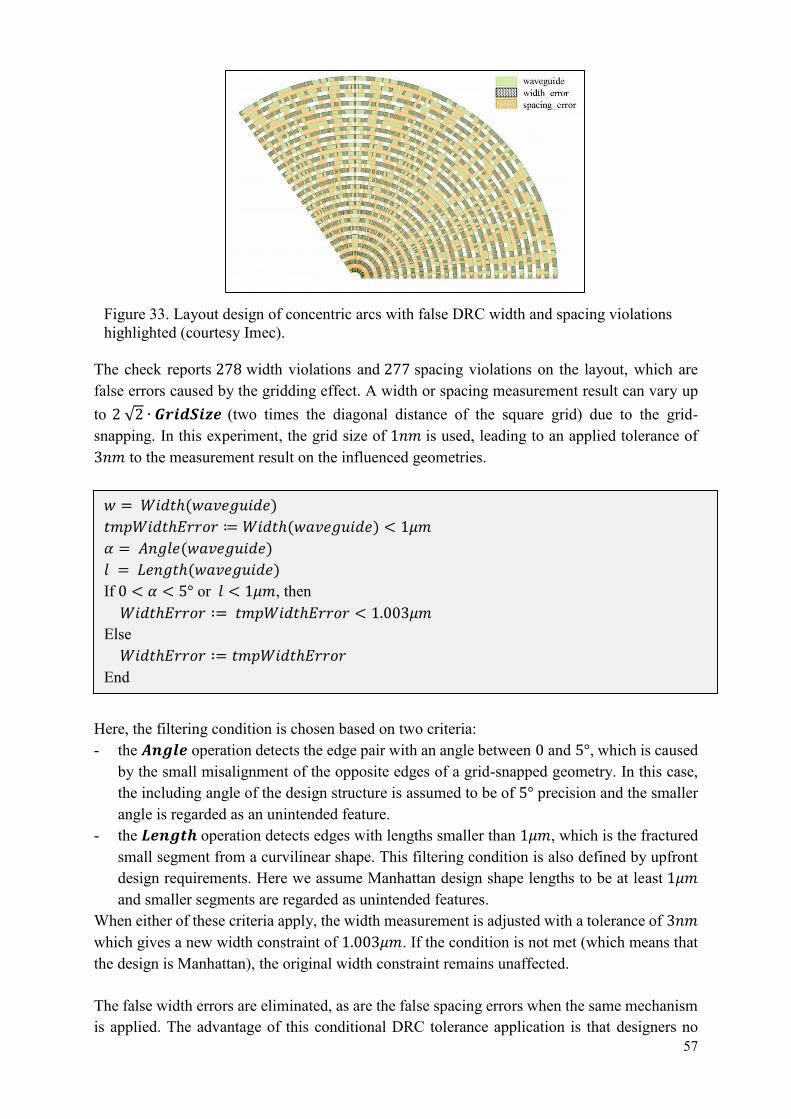
57
The check reports 278 width violations and 277 spacing violations on the layout, which are false errors caused by the gridding effect. A width or spacing measurement result can vary up to 2 √2 ∙ 𝑮𝒓𝒊𝒅𝑺𝒊𝒛𝒆 (two times the diagonal distance of the square grid) due to the grid-snapping. In this experiment, the grid size of 1𝑛𝑚 is used, leading to an applied tolerance of 3𝑛𝑚 to the measurement result on the influenced geometries.
Here, the filtering condition is chosen based on two criteria: - the 𝑨𝒏𝒈𝒍𝒆 operation detects the edge pair with an angle between 0 and 5°, which is caused
by the small misalignment of the opposite edges of a grid-snapped geometry. In this case, the including angle of the design structure is assumed to be of 5° precision and the smaller angle is regarded as an unintended feature.
- the 𝑳𝒆𝒏𝒈𝒕𝒉 operation detects edges with lengths smaller than 1𝜇𝑚, which is the fractured small segment from a curvilinear shape. This filtering condition is also defined by upfront design requirements. Here we assume Manhattan design shape lengths to be at least 1𝜇𝑚 and smaller segments are regarded as unintended features.
When either of these criteria apply, the width measurement is adjusted with a tolerance of 3𝑛𝑚 which gives a new width constraint of 1.003𝜇𝑚. If the condition is not met (which means that the design is Manhattan), the original width constraint remains unaffected. The false width errors are eliminated, as are the false spacing errors when the same mechanism is applied. The advantage of this conditional DRC tolerance application is that designers no
Figure 33. Layout design of concentric arcs with false DRC width and spacing violations highlighted (courtesy Imec).
𝑤 = 𝑊𝑖𝑑𝑡ℎ(𝑤𝑎𝑣𝑒𝑔𝑢𝑖𝑑𝑒) 𝑡𝑚𝑝𝑊𝑖𝑑𝑡ℎ𝐸𝑟𝑟𝑜𝑟 ≔ 𝑊𝑖𝑑𝑡ℎ(𝑤𝑎𝑣𝑒𝑔𝑢𝑖𝑑𝑒) < 1𝜇𝑚 𝛼 = 𝐴𝑛𝑔𝑙𝑒(𝑤𝑎𝑣𝑒𝑔𝑢𝑖𝑑𝑒) 𝑙 = 𝐿𝑒𝑛𝑔𝑡ℎ(𝑤𝑎𝑣𝑒𝑔𝑢𝑖𝑑𝑒) If 0 < 𝛼 < 5° or 𝑙 < 1𝜇𝑚, then
𝑊𝑖𝑑𝑡ℎ𝐸𝑟𝑟𝑜𝑟 ∶= 𝑡𝑚𝑝𝑊𝑖𝑑𝑡ℎ𝐸𝑟𝑟𝑜𝑟 < 1.003𝜇𝑚 Else
𝑊𝑖𝑑𝑡ℎ𝐸𝑟𝑟𝑜𝑟 ∶= 𝑡𝑚𝑝𝑊𝑖𝑑𝑡ℎ𝐸𝑟𝑟𝑜𝑟 End
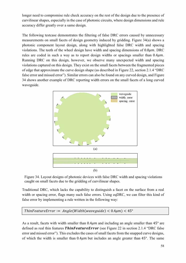
58
longer need to compromise rule check accuracy on the rest of the design due to the presence of curvilinear shapes, especially in the case of photonic circuits, where design dimensions and rule accuracy differ greatly over a same design. The following testcase demonstrates the filtering of false DRC errors caused by unnecessary measurements on small facets of design geometry induced by gridding. Figure 34(a) shows a photonic component layout design, along with highlighted false DRC width and spacing violations. The teeth of the wheel design have width and spacing dimensions of 0.8𝜇𝑚. DRC rules are coded in such a way as to report design widths or spacings smaller than 0.4𝜇𝑚. Running DRC on this design, however, we observe many unexpected width and spacing violations captured on this design. They exist on the small facets between the fragmented pieces of edge that approximate the curve design shape (as described in Figure 22, section 2.1.4 “DRC false error and missed error”). Similar errors can also be found on any curved design, and Figure 34 shows another example of DRC reporting width errors on the small facets of a long curved waveguide.
Traditional DRC, which lacks the capability to distinguish a facet on the surface from a real width or spacing error, flags many such false errors. Using eqDRC, we can filter this kind of false error by implementing a rule written in the following way:
As a result, facets with width smaller than 0.4𝜇𝑚 and including an angle smaller than 45° are defined as real thin features 𝑻𝒉𝒊𝒏𝑭𝒆𝒂𝒕𝒖𝒓𝒆𝑬𝒓𝒓𝒐𝒓 (see Figure 22 in section 2.1.4 “DRC false error and missed error”). This excludes the cases of small facets from the snapped curve designs, of which the width is smaller than 0.4𝜇𝑚 but includes an angle greater than 45°. The same
(a)
(b)
Figure 34. Layout designs of photonic devices with false DRC width and spacing violations caught on small facets due to the gridding of curvilinear shapes.
𝑇ℎ𝑖𝑛𝐹𝑒𝑎𝑡𝑢𝑟𝑒𝐸𝑟𝑟𝑜𝑟 ∶= 𝐴𝑛𝑔𝑙𝑒(𝑊𝑖𝑑𝑡ℎ(𝑤𝑎𝑣𝑒𝑔𝑢𝑖𝑑𝑒) < 0.4𝜇𝑚) < 45°
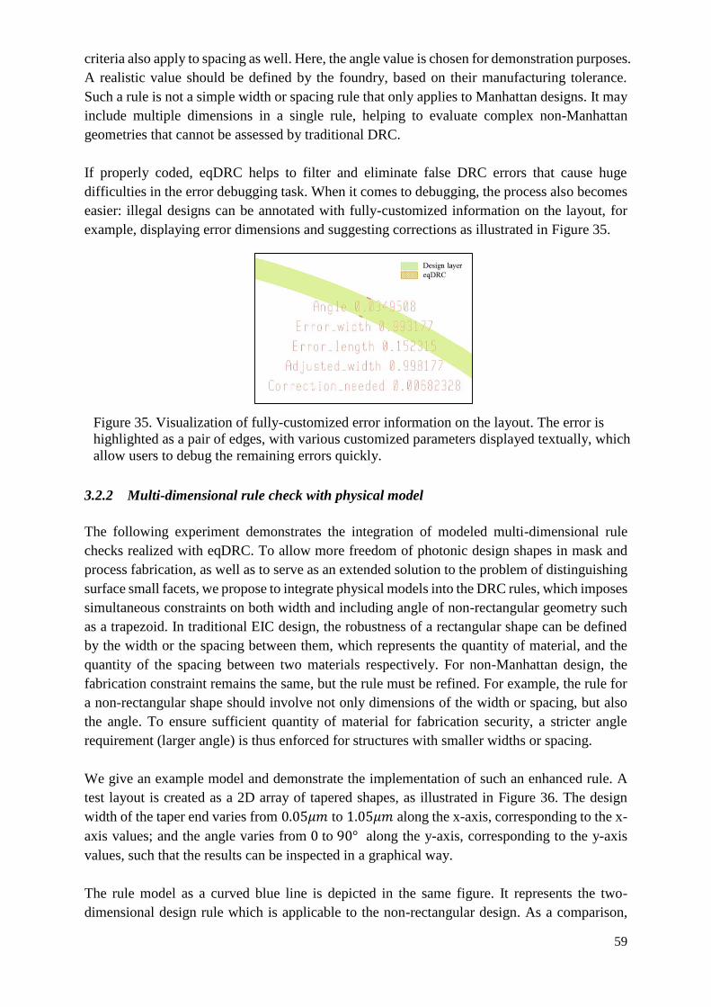
59
criteria also apply to spacing as well. Here, the angle value is chosen for demonstration purposes.
A realistic value should be defined by the foundry, based on their manufacturing tolerance.
Such a rule is not a simple width or spacing rule that only applies to Manhattan designs. It may
include multiple dimensions in a single rule, helping to evaluate complex non-Manhattan
geometries that cannot be assessed by traditional DRC.
If properly coded, eqDRC helps to filter and eliminate false DRC errors that cause huge
difficulties in the error debugging task. When it comes to debugging, the process also becomes
easier: illegal designs can be annotated with fully-customized information on the layout, for
example, displaying error dimensions and suggesting corrections as illustrated in Figure 35.
3.2.2 Multi-dimensional rule check with physical model
The following experiment demonstrates the integration of modeled multi-dimensional rule
checks realized with eqDRC. To allow more freedom of photonic design shapes in mask and
process fabrication, as well as to serve as an extended solution to the problem of distinguishing
surface small facets, we propose to integrate physical models into the DRC rules, which imposes
simultaneous constraints on both width and including angle of non-rectangular geometry such
as a trapezoid. In traditional EIC design, the robustness of a rectangular shape can be defined
by the width or the spacing between them, which represents the quantity of material, and the
quantity of the spacing between two materials respectively. For non-Manhattan design, the
fabrication constraint remains the same, but the rule must be refined. For example, the rule for
a non-rectangular shape should involve not only dimensions of the width or spacing, but also
the angle. To ensure sufficient quantity of material for fabrication security, a stricter angle
requirement (larger angle) is thus enforced for structures with smaller widths or spacing.
We give an example model and demonstrate the implementation of such an enhanced rule. A
test layout is created as a 2D array of tapered shapes, as illustrated in Figure 36. The design
width of the taper end varies from 0.05𝜇𝑚 to 1.05𝜇𝑚 along the x-axis, corresponding to the x-
axis values; and the angle varies from 0 to 90° along the y-axis, corresponding to the y-axis
values, such that the results can be inspected in a graphical way.
The rule model as a curved blue line is depicted in the same figure. It represents the two-
dimensional design rule which is applicable to the non-rectangular design. As a comparison,
Figure 35. Visualization of fully-customized error information on the layout. The error is
highlighted as a pair of edges, with various customized parameters displayed textually, which
allow users to debug the remaining errors quickly.
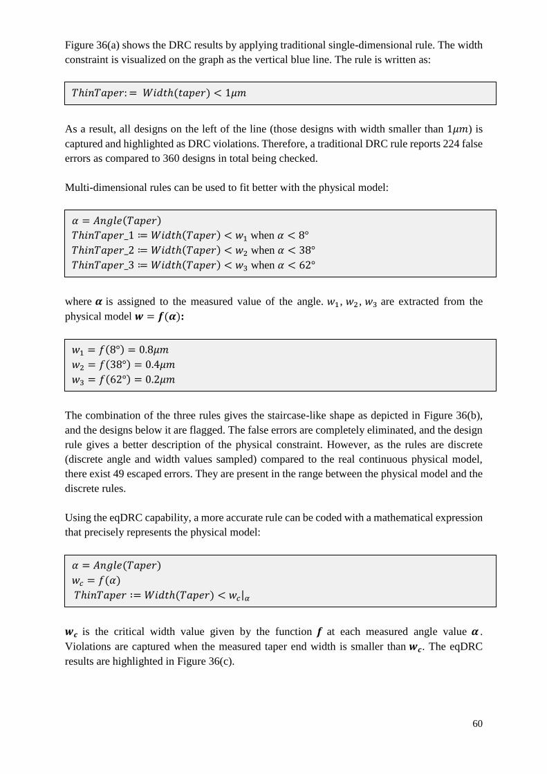
60
Figure 36(a) shows the DRC results by applying traditional single-dimensional rule. The width
constraint is visualized on the graph as the vertical blue line. The rule is written as:
As a result, all designs on the left of the line (those designs with width smaller than 1𝜇𝑚) is
captured and highlighted as DRC violations. Therefore, a traditional DRC rule reports 224 false
errors as compared to 360 designs in total being checked.
Multi-dimensional rules can be used to fit better with the physical model:
where 𝜶 is assigned to the measured value of the angle. 𝑤1, 𝑤2 , 𝑤3 are extracted from the
physical model 𝒘 = 𝒇(𝜶):
The combination of the three rules gives the staircase-like shape as depicted in Figure 36(b),
and the designs below it are flagged. The false errors are completely eliminated, and the design
rule gives a better description of the physical constraint. However, as the rules are discrete
(discrete angle and width values sampled) compared to the real continuous physical model,
there exist 49 escaped errors. They are present in the range between the physical model and the
discrete rules.
Using the eqDRC capability, a more accurate rule can be coded with a mathematical expression
that precisely represents the physical model:
𝒘𝒄 is the critical width value given by the function 𝒇 at each measured angle value 𝜶 .
Violations are captured when the measured taper end width is smaller than 𝒘𝒄. The eqDRC
results are highlighted in Figure 36(c).
𝑇ℎ𝑖𝑛𝑇𝑎𝑝𝑒𝑟: = 𝑊𝑖𝑑𝑡ℎ(𝑡𝑎𝑝𝑒𝑟) < 1𝜇𝑚
𝛼 = 𝐴𝑛𝑔𝑙𝑒(𝑇𝑎𝑝𝑒𝑟)
𝑇ℎ𝑖𝑛𝑇𝑎𝑝𝑒𝑟_1 ≔ 𝑊𝑖𝑑𝑡ℎ(𝑇𝑎𝑝𝑒𝑟) < 𝑤1 when 𝛼 < 8°
𝑇ℎ𝑖𝑛𝑇𝑎𝑝𝑒𝑟_2 ≔ 𝑊𝑖𝑑𝑡ℎ(𝑇𝑎𝑝𝑒𝑟) < 𝑤2 when 𝛼 < 38°
𝑇ℎ𝑖𝑛𝑇𝑎𝑝𝑒𝑟_3 ≔ 𝑊𝑖𝑑𝑡ℎ(𝑇𝑎𝑝𝑒𝑟) < 𝑤3 when 𝛼 < 62°
𝑤1 = 𝑓(8°) = 0.8𝜇𝑚
𝑤2 = 𝑓(38°) = 0.4𝜇𝑚
𝑤3 = 𝑓(62°) = 0.2𝜇𝑚
𝛼 = 𝐴𝑛𝑔𝑙𝑒(𝑇𝑎𝑝𝑒𝑟)
𝑤𝑐 = 𝑓(𝛼)
𝑇ℎ𝑖𝑛𝑇𝑎𝑝𝑒𝑟 ∶= 𝑊𝑖𝑑𝑡ℎ(𝑇𝑎𝑝𝑒𝑟) < 𝑤𝑐|𝛼
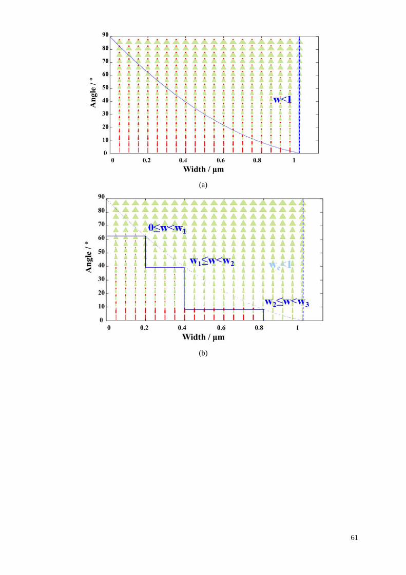
61
(a)
(b)
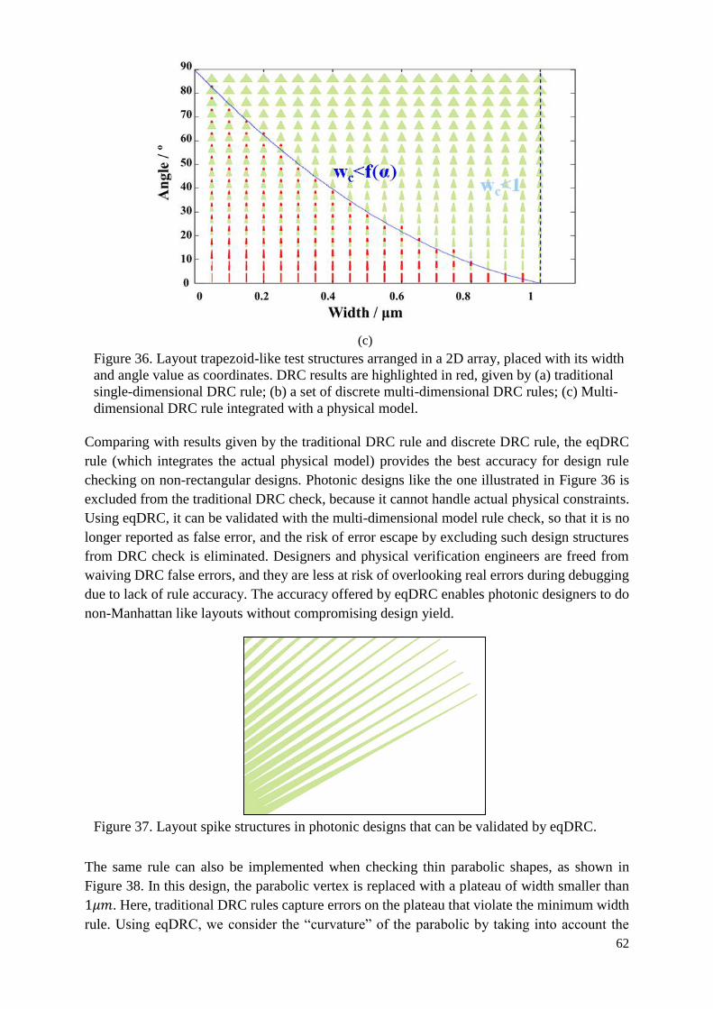
62
Comparing with results given by the traditional DRC rule and discrete DRC rule, the eqDRC
rule (which integrates the actual physical model) provides the best accuracy for design rule
checking on non-rectangular designs. Photonic designs like the one illustrated in Figure 36 is
excluded from the traditional DRC check, because it cannot handle actual physical constraints.
Using eqDRC, it can be validated with the multi-dimensional model rule check, so that it is no
longer reported as false error, and the risk of error escape by excluding such design structures
from DRC check is eliminated. Designers and physical verification engineers are freed from
waiving DRC false errors, and they are less at risk of overlooking real errors during debugging
due to lack of rule accuracy. The accuracy offered by eqDRC enables photonic designers to do
non-Manhattan like layouts without compromising design yield.
The same rule can also be implemented when checking thin parabolic shapes, as shown in
Figure 38. In this design, the parabolic vertex is replaced with a plateau of width smaller than
1𝜇𝑚. Here, traditional DRC rules capture errors on the plateau that violate the minimum width
rule. Using eqDRC, we consider the “curvature” of the parabolic by taking into account the
(c)
Figure 36. Layout trapezoid-like test structures arranged in a 2D array, placed with its width
and angle value as coordinates. DRC results are highlighted in red, given by (a) traditional
single-dimensional DRC rule; (b) a set of discrete multi-dimensional DRC rules; (c) Multi-
dimensional DRC rule integrated with a physical model.
Figure 37. Layout spike structures in photonic designs that can be validated by eqDRC.
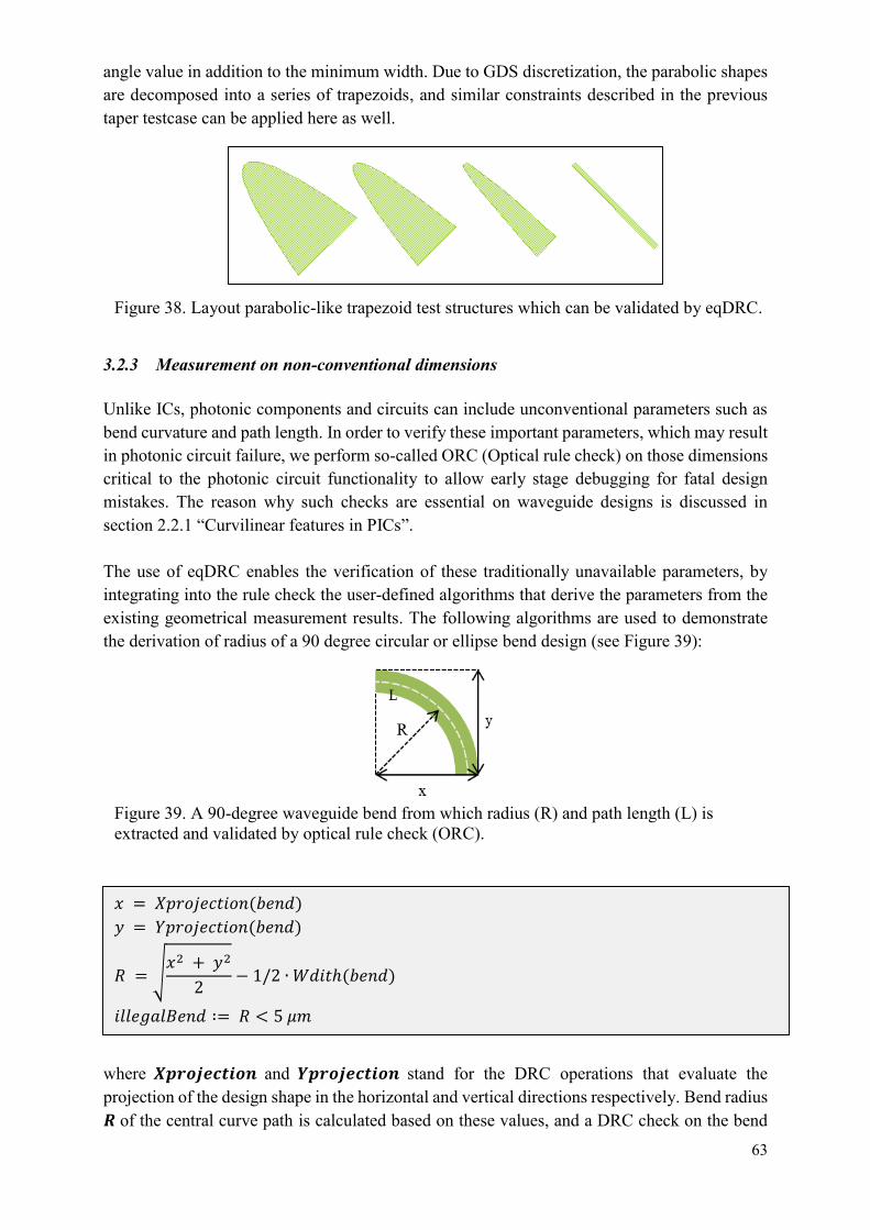
63
angle value in addition to the minimum width. Due to GDS discretization, the parabolic shapes are decomposed into a series of trapezoids, and similar constraints described in the previous taper testcase can be applied here as well.
3.2.3 Measurement on non-conventional dimensions Unlike ICs, photonic components and circuits can include unconventional parameters such as bend curvature and path length. In order to verify these important parameters, which may result in photonic circuit failure, we perform so-called ORC (Optical rule check) on those dimensions critical to the photonic circuit functionality to allow early stage debugging for fatal design mistakes. The reason why such checks are essential on waveguide designs is discussed in section 2.2.1 “Curvilinear features in PICs”. The use of eqDRC enables the verification of these traditionally unavailable parameters, by integrating into the rule check the user-defined algorithms that derive the parameters from the existing geometrical measurement results. The following algorithms are used to demonstrate the derivation of radius of a 90 degree circular or ellipse bend design (see Figure 39):
where 𝑿𝒑𝒓𝒐𝒋𝒆𝒄𝒕𝒊𝒐𝒏 and 𝒀𝒑𝒓𝒐𝒋𝒆𝒄𝒕𝒊𝒐𝒏 stand for the DRC operations that evaluate the projection of the design shape in the horizontal and vertical directions respectively. Bend radius 𝑹 of the central curve path is calculated based on these values, and a DRC check on the bend
Figure 38. Layout parabolic-like trapezoid test structures which can be validated by eqDRC.
Figure 39. A 90-degree waveguide bend from which radius (R) and path length (L) is extracted and validated by optical rule check (ORC).
𝑥 = 𝑋𝑝𝑟𝑜𝑗𝑒𝑐𝑡𝑖𝑜𝑛(𝑏𝑒𝑛𝑑) 𝑦 = 𝑌𝑝𝑟𝑜𝑗𝑒𝑐𝑡𝑖𝑜𝑛(𝑏𝑒𝑛𝑑)
𝑅 = √𝑥2 + 𝑦2
2− 1/2 ∙ 𝑊𝑑𝑖𝑡ℎ(𝑏𝑒𝑛𝑑)
𝑖𝑙𝑙𝑒𝑔𝑎𝑙𝐵𝑒𝑛𝑑 ∶= 𝑅 < 5 𝜇𝑚
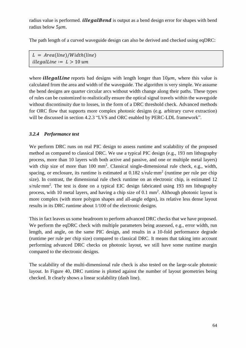
64
radius value is performed. 𝒊𝒍𝒍𝒆𝒈𝒂𝒍𝑩𝒆𝒏𝒅 is output as a bend design error for shapes with bend
radius below 5𝜇𝑚.
The path length of a curved waveguide design can also be derived and checked using eqDRC:
where 𝒊𝒍𝒍𝒆𝒈𝒂𝒍𝑳𝒊𝒏𝒆 reports bad designs with length longer than 10𝜇𝑚, where this value is
calculated from the area and width of the waveguide. The algorithm is very simple. We assume
the bend designs are quarter circular arcs without width change along their paths. These types
of rules can be customized to realistically ensure the optical signal travels within the waveguide
without discontinuity due to losses, in the form of a DRC threshold check. Advanced methods
for ORC flow that supports more complex photonic designs (e.g. arbitrary curve extraction)
will be discussed in section 4.2.3 “LVS and ORC enabled by PERC-LDL framework”.
3.2.4 Performance test
We perform DRC runs on real PIC design to assess runtime and scalability of the proposed
method as compared to classical DRC. We use a typical PIC design (e.g., 193 nm lithography
process, more than 10 layers with both active and passive, and one or multiple metal layers)
with chip size of more than 100 mm2. Classical single-dimensional rule check, e.g., width,
spacing, or enclosure, its runtime is estimated at 0.182 s/rule∙mm2 (runtime per rule per chip
size). In contrast, the dimensional rule check runtime on an electronic chip, is estimated 12
s/rule∙mm2. The test is done on a typical EIC design fabricated using 193 nm lithography
process, with 10 metal layers, and having a chip size of 0.1 mm2. Although photonic layout is
more complex (with more polygon shapes and all-angle edges), its relative less dense layout
results in its DRC runtime about 1/100 of the electronic designs.
This in fact leaves us some headroom to perform advanced DRC checks that we have proposed.
We perform the eqDRC check with multiple parameters being assessed, e.g., error width, run
length, and angle, on the same PIC design, and results in a 10-fold performance degrade
(runtime per rule per chip size) compared to classical DRC. It means that taking into account
performing advanced DRC checks on photonic layout, we still have some runtime margin
compared to the electronic designs.
The scalability of the multi-dimensional rule check is also tested on the large-scale photonic
layout. In Figure 40, DRC runtime is plotted against the number of layout geometries being
checked. It clearly shows a linear scalability (dash line).
𝐿 = 𝐴𝑟𝑒𝑎(𝑙𝑖𝑛𝑒)/𝑊𝑖𝑑𝑡ℎ(𝑙𝑖𝑛𝑒)
𝑖𝑙𝑙𝑒𝑔𝑎𝑙𝐿𝑖𝑛𝑒 ∶= 𝐿 > 10 𝑢𝑚
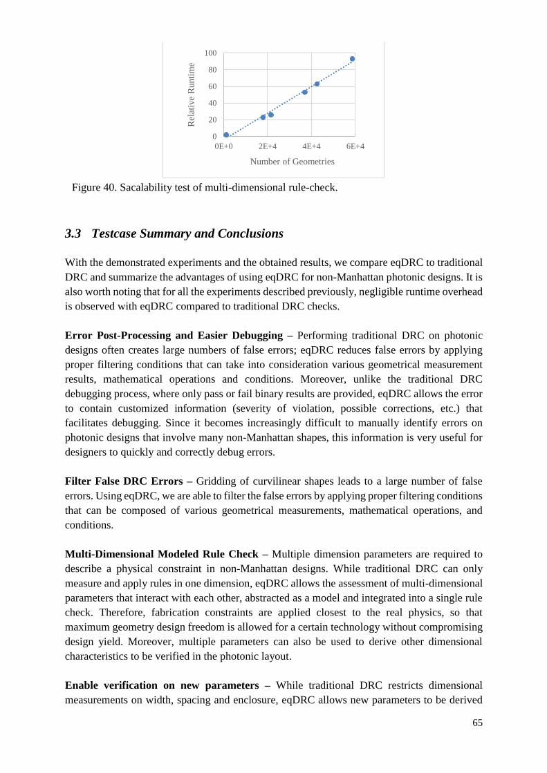
65
3.3 Testcase Summary and Conclusions
With the demonstrated experiments and the obtained results, we compare eqDRC to traditional
DRC and summarize the advantages of using eqDRC for non-Manhattan photonic designs. It is
also worth noting that for all the experiments described previously, negligible runtime overhead
is observed with eqDRC compared to traditional DRC checks.
Error Post-Processing and Easier Debugging – Performing traditional DRC on photonic
designs often creates large numbers of false errors; eqDRC reduces false errors by applying
proper filtering conditions that can take into consideration various geometrical measurement
results, mathematical operations and conditions. Moreover, unlike the traditional DRC
debugging process, where only pass or fail binary results are provided, eqDRC allows the error
to contain customized information (severity of violation, possible corrections, etc.) that
facilitates debugging. Since it becomes increasingly difficult to manually identify errors on
photonic designs that involve many non-Manhattan shapes, this information is very useful for
designers to quickly and correctly debug errors.
Filter False DRC Errors – Gridding of curvilinear shapes leads to a large number of false
errors. Using eqDRC, we are able to filter the false errors by applying proper filtering conditions
that can be composed of various geometrical measurements, mathematical operations, and
conditions.
Multi-Dimensional Modeled Rule Check – Multiple dimension parameters are required to
describe a physical constraint in non-Manhattan designs. While traditional DRC can only
measure and apply rules in one dimension, eqDRC allows the assessment of multi-dimensional
parameters that interact with each other, abstracted as a model and integrated into a single rule
check. Therefore, fabrication constraints are applied closest to the real physics, so that
maximum geometry design freedom is allowed for a certain technology without compromising
design yield. Moreover, multiple parameters can also be used to derive other dimensional
characteristics to be verified in the photonic layout.
Enable verification on new parameters – While traditional DRC restricts dimensional
measurements on width, spacing and enclosure, eqDRC allows new parameters to be derived
Figure 40. Sacalability test of multi-dimensional rule-check.
0
20
40
60
80
100
0E+0 2E+4 4E+4 6E+4
Rel
ativ
e R
unti
me
Number of Geometries
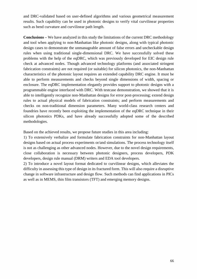
66
and DRC-validated based on user-defined algorithms and various geometrical measurement
results. Such capability can be used in photonic designs to verify vital curvilinear properties
such as bend curvature and curvilinear path length.
Conclusions – We have analyzed in this study the limitations of the current DRC methodology
and tool when applying to non-Manhattan like photonic designs, along with typical photonic
design cases to demonstrate the unmanageable amount of false errors and uncheckable design
rules when using traditional single-dimensional DRC. We have successfully solved these
problems with the help of the eqDRC, which was previously developed for EIC design rule
check at advanced nodes. Though advanced technology platforms (and associated stringent
fabrication constraints) are not required (or suitable) for silicon photonics, the non-Manhattan
characteristics of the photonic layout requires an extended capability DRC engine. It must be
able to perform measurements and checks beyond single dimensions of width, spacing or
enclosure. The eqDRC implementation elegantly provides support to photonic designs with a
programmable engine interfaced with DRC. With testcase demonstration, we showed that it is
able to intelligently recognize non-Manhattan designs for error post-processing; extend design
rules to actual physical models of fabrication constraints; and perform measurements and
checks on non-traditional dimension parameters. Many world-class research centers and
foundries have recently been exploiting the implementation of the eqDRC technique in their
silicon photonics PDKs, and have already successfully adopted some of the described
methodologies.
Based on the achieved results, we propose future studies in this area including:
1) To extensively verbalize and formulate fabrication constraints for non-Manhattan layout
designs based on actual process experiments or/and simulations. The process technology itself
is not as challenging as other advanced nodes. However, due to the novel design requirements,
close collaboration is necessary between photonic designers, process developers, PDK
developers, design rule manual (DRM) writers and EDA tool developers.
2) To introduce a novel layout format dedicated to curvilinear designs, which alleviates the
difficulty in assessing this type of design in its fractured form. This will also require a disruptive
change in software infrastructure and design flow. Such methods can find applications in PICs
as well as in MEMS, thin film transistors (TFT) and emerging memory designs.

67
Chapter 4 LAYOUT VS. SCHEMATIC (LVS) CHECKING
Due to lack of the LVS methodologies specific to photonic design validation requirements,
current LVS flows run by silicon photonics foundries have very limited verification capabilities,
or are simply not used due to the lack of an appropriate LVS tool or rule deck.
We will start this chapter by introducing a black-box LVS flow, from which users can detect
circuit topology corruptions such as unintended shorts or opens that may otherwise be missed.
According to the circuit validation requirements analyzed in Chapter 2 “PV for Photonic
Designs – Requirements and Limitations”, we introduce LVS methods and flows that are
dedicated to verifying photonic layouts. Corresponding methods are proposed to validate
different photonic layout elements: critical or non-critical waveguide interconnect, and photonic
devices with curved features. With such validation, it is now possible to ensure the drawn
elements in the layout correctly match the user-specified design intent, and follow certain
optical design rules.
4.1 Black-Box LVS
Although many features are missing for photonic device and circuit validation due to the distinct
nature of photonic designs, a primary step that performs circuit topology check for unintended
shorts or opens can be implemented by classical LVS tools. This requires the development of
the LVS rule deck and imposes some requirements on the upstream design flow.
We recommend black-box LVS to be implemented for photonic circuit validation as a minimum
requirement. The goal of black-box LVS is to check the device type, count, and the pin
connections. At this stage, the content of the cell is ignored and is treated as a primitive device
with pins. Photonic-specific verification requirements are not yet considered, and thereby the
related difficulties are avoided.
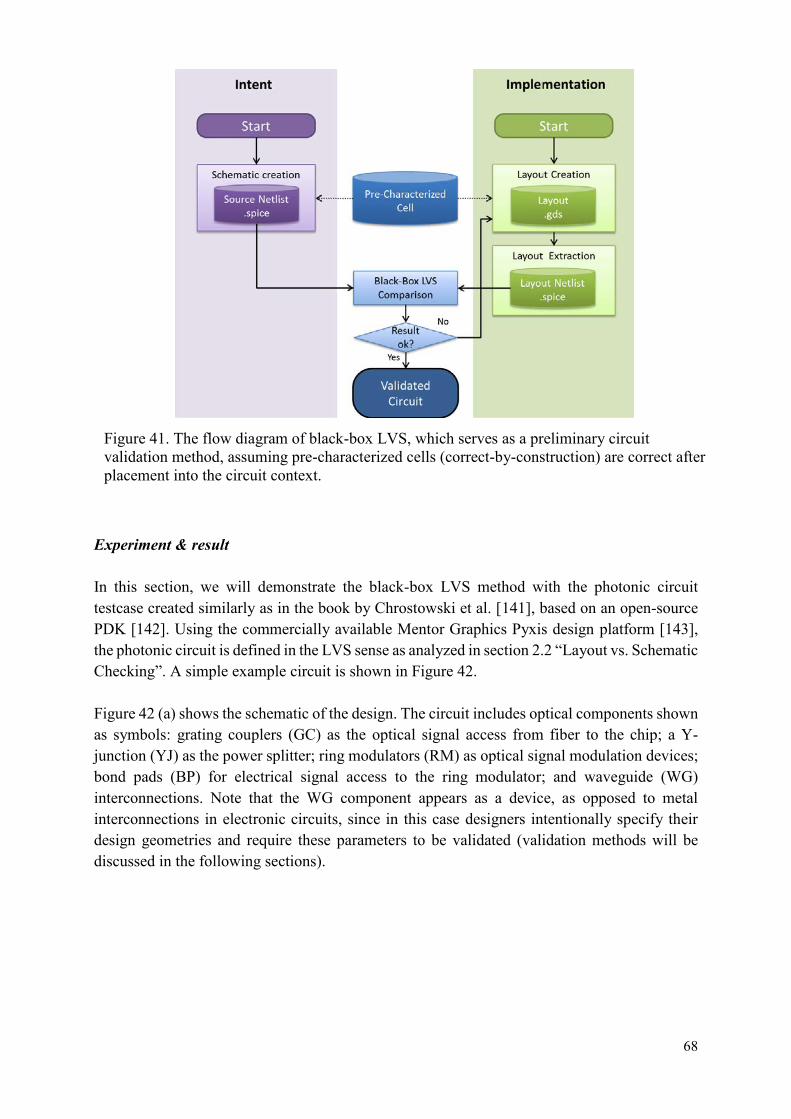
68
Experiment & result In this section, we will demonstrate the black-box LVS method with the photonic circuit testcase created similarly as in the book by Chrostowski et al. [141], based on an open-source PDK [142]. Using the commercially available Mentor Graphics Pyxis design platform [143], the photonic circuit is defined in the LVS sense as analyzed in section 2.2 “Layout vs. Schematic Checking”. A simple example circuit is shown in Figure 42. Figure 42 (a) shows the schematic of the design. The circuit includes optical components shown as symbols: grating couplers (GC) as the optical signal access from fiber to the chip; a Y-junction (YJ) as the power splitter; ring modulators (RM) as optical signal modulation devices; bond pads (BP) for electrical signal access to the ring modulator; and waveguide (WG) interconnections. Note that the WG component appears as a device, as opposed to metal interconnections in electronic circuits, since in this case designers intentionally specify their design geometries and require these parameters to be validated (validation methods will be discussed in the following sections).
Figure 41. The flow diagram of black-box LVS, which serves as a preliminary circuit validation method, assuming pre-characterized cells (correct-by-construction) are correct after placement into the circuit context.
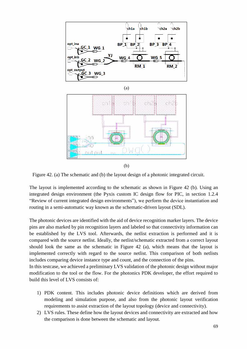
69
The layout is implemented according to the schematic as shown in Figure 42 (b). Using an
integrated design environment (the Pyxis custom IC design flow for PIC, in section 1.2.4
“Review of current integrated design environments”), we perform the device instantiation and
routing in a semi-automatic way known as the schematic-driven layout (SDL).
The photonic devices are identified with the aid of device recognition marker layers. The device
pins are also marked by pin recognition layers and labeled so that connectivity information can
be established by the LVS tool. Afterwards, the netlist extraction is performed and it is
compared with the source netlist. Ideally, the netlist/schematic extracted from a correct layout
should look the same as the schematic in Figure 42 (a), which means that the layout is
implemented correctly with regard to the source netlist. This comparison of both netlists
includes comparing device instance type and count, and the connection of the pins.
In this testcase, we achieved a preliminary LVS validation of the photonic design without major
modification to the tool or the flow. For the photonics PDK developer, the effort required to
build this level of LVS consists of:
1) PDK content. This includes photonic device definitions which are derived from
modeling and simulation purpose, and also from the photonic layout verification
requirements to assist extraction of the layout topology (device and connectivity).
2) LVS rules. These define how the layout devices and connectivity are extracted and how
the comparison is done between the schematic and layout.
(a)
(b)
Figure 42. (a) The schematic and (b) the layout design of a photonic integrated circuit.
70
Black-box LVS performs analysis by comparing only the connections at the top level of the box
cells. The error is detected in basic circuit topologies, such as wrong or missing/excess
placement of devices, or wrong connections. Generally, the black box approach is not
recommended for tape-out LVS verification runs, as black boxes can obscure design
discrepancies. Although the placed cells are foundry-approved building blocks that are “correct-
by-construction” (CBC), errors can happen, i.e. during the cell placement into the circuit context.
In case of photonic designs, since there is no existing methodology to validate photonic device
content, we recommend this black-box LVS as the primary circuit verification method. We will
introduce more advanced methods that are developed based on this flow.
4.2 Waveguide Interconnect Validation
In the proposed black-box LVS method, device content is screened from validation due to the
lack of tool capabilities to verify curved features. In this section, we first demonstrate the
developed approach for measuring waveguide interconnect with curvilinear geometry. It is
based on the classical LVS tools and the commonly used SPICE netlist that is the standard
netlist format in the EIC design flow.
Layout waveguide interconnect can be characterized by its width, path length, and bend radius
values (as described in section 2.2.3 “Representation of photonic device feature in standard
netlist format”). Once these parameters are measured, they are then validated by
1) Comparison to the source parameters, when the waveguide interconnect is critical to the
circuit behavior (e.g. in an MZI phase shifter circuit) and designers carefully place those
interconnects with specified source parameters.
2) Checks against optical design constraints, or optical rule check (ORC) as we proposed.
In the case of non-critical waveguide interconnect, the design geometry is not
intentionally specified and there is no source information. Nevertheless, optical signal
integrity related design constraints must be obeyed (section 2.2.1 “Curvilinear features
in PICs”) and should be considered in post-layout simulation if needed.
In both cases, the curvilinear features of the waveguide interconnect must first be measured,
which is not available from the existing LVS tools. We will first introduce the methods
developed that extend the tool capability to measure waveguide interconnect curvilinear
features like path length and curvature. Then we will present the flow integrations for validating
waveguide interconnect designs based on these measurement results, considering different
design and verification goals.
4.2.1 Method I
We explore various methods for curvilinear feature extraction and will conclude the pros and
cons for each. We demonstrate this method using the Calibre nmLVS tool, using its
programmable interface for computing the measurable dimensions obtained from the graphical
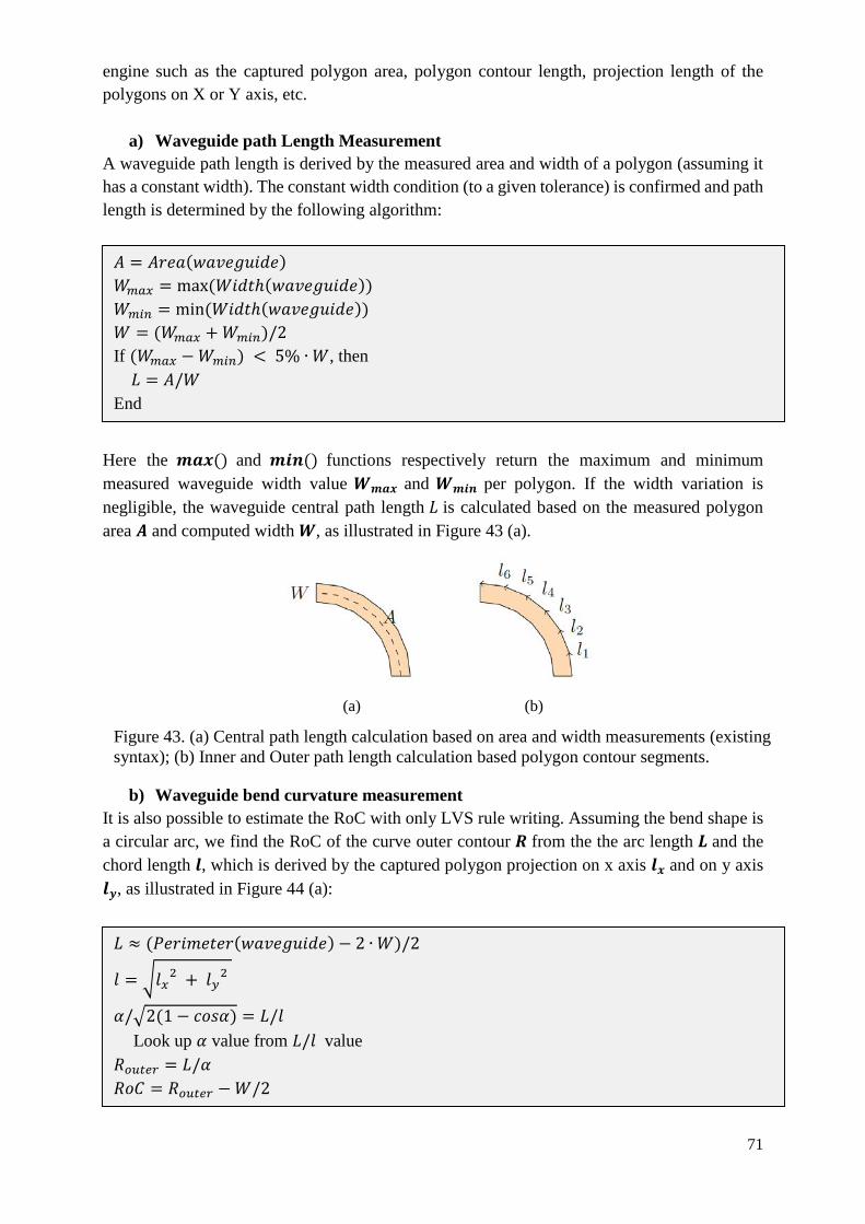
71
engine such as the captured polygon area, polygon contour length, projection length of the
polygons on X or Y axis, etc.
a) Waveguide path Length Measurement
A waveguide path length is derived by the measured area and width of a polygon (assuming it
has a constant width). The constant width condition (to a given tolerance) is confirmed and path
length is determined by the following algorithm:
Here the 𝒎𝒂𝒙 () and 𝒎𝒊𝒏() functions respectively return the maximum and minimum
measured waveguide width value 𝑾𝒎𝒂𝒙 and 𝑾𝒎𝒊𝒏 per polygon. If the width variation is
negligible, the waveguide central path length 𝐿 is calculated based on the measured polygon
area 𝑨 and computed width 𝑾, as illustrated in Figure 43 (a).
b) Waveguide bend curvature measurement
It is also possible to estimate the RoC with only LVS rule writing. Assuming the bend shape is
a circular arc, we find the RoC of the curve outer contour 𝑹 from the the arc length 𝑳 and the
chord length 𝒍, which is derived by the captured polygon projection on x axis 𝒍𝒙 and on y axis
𝒍𝒚, as illustrated in Figure 44 (a):
𝐴 = 𝐴𝑟𝑒𝑎(𝑤𝑎𝑣𝑒𝑔𝑢𝑖𝑑𝑒)
𝑊𝑚𝑎𝑥 = max (𝑊𝑖𝑑𝑡ℎ(𝑤𝑎𝑣𝑒𝑔𝑢𝑖𝑑𝑒))
𝑊𝑚𝑖𝑛 = min(𝑊𝑖𝑑𝑡ℎ(𝑤𝑎𝑣𝑒𝑔𝑢𝑖𝑑𝑒))
𝑊 = (𝑊𝑚𝑎𝑥 + 𝑊𝑚𝑖𝑛)/2
If (𝑊𝑚𝑎𝑥 − 𝑊𝑚𝑖𝑛) < 5% ∙ 𝑊, then
𝐿 = 𝐴/𝑊
End
(a) (b)
Figure 43. (a) Central path length calculation based on area and width measurements (existing
syntax); (b) Inner and Outer path length calculation based polygon contour segments.
𝐿 ≈ (𝑃𝑒𝑟𝑖𝑚𝑒𝑡𝑒𝑟(𝑤𝑎𝑣𝑒𝑔𝑢𝑖𝑑𝑒) − 2 ∙ 𝑊)/2
𝑙 = √𝑙𝑥2 + 𝑙𝑦
2
𝛼/√2(1 − 𝑐𝑜𝑠𝛼) = 𝐿/𝑙
Look up 𝛼 value from 𝐿/𝑙 value
𝑅𝑜𝑢𝑡𝑒𝑟 = 𝐿/𝛼
𝑅𝑜𝐶 = 𝑅𝑜𝑢𝑡𝑒𝑟 − 𝑊/2
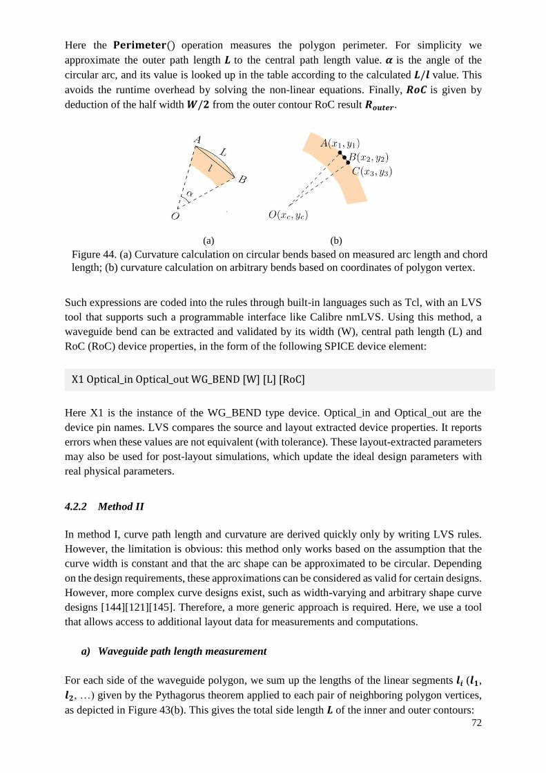
72
Here the 𝐏𝐞𝐫𝐢𝐦𝐞𝐭𝐞𝐫() operation measures the polygon perimeter. For simplicity we
approximate the outer path length 𝑳 to the central path length value. 𝜶 is the angle of the
circular arc, and its value is looked up in the table according to the calculated 𝑳/𝒍 value. This
avoids the runtime overhead by solving the non-linear equations. Finally, 𝑹𝒐𝑪 is given by
deduction of the half width 𝑾/𝟐 from the outer contour RoC result 𝑹𝒐𝒖𝒕𝒆𝒓.
Such expressions are coded into the rules through built-in languages such as Tcl, with an LVS
tool that supports such a programmable interface like Calibre nmLVS. Using this method, a
waveguide bend can be extracted and validated by its width (W), central path length (L) and
RoC (RoC) device properties, in the form of the following SPICE device element:
Here X1 is the instance of the WG_BEND type device. Optical_in and Optical_out are the
device pin names. LVS compares the source and layout extracted device properties. It reports
errors when these values are not equivalent (with tolerance). These layout-extracted parameters
may also be used for post-layout simulations, which update the ideal design parameters with
real physical parameters.
4.2.2 Method II
In method I, curve path length and curvature are derived quickly only by writing LVS rules.
However, the limitation is obvious: this method only works based on the assumption that the
curve width is constant and that the arc shape can be approximated to be circular. Depending
on the design requirements, these approximations can be considered as valid for certain designs.
However, more complex curve designs exist, such as width-varying and arbitrary shape curve
designs [144][121][145]. Therefore, a more generic approach is required. Here, we use a tool
that allows access to additional layout data for measurements and computations.
a) Waveguide path length measurement
For each side of the waveguide polygon, we sum up the lengths of the linear segments 𝒍𝒊 (𝒍𝟏,
𝒍𝟐, …) given by the Pythagorus theorem applied to each pair of neighboring polygon vertices,
as depicted in Figure 43(b). This gives the total side length 𝑳 of the inner and outer contours:
(a) (b)
Figure 44. (a) Curvature calculation on circular bends based on measured arc length and chord
length; (b) curvature calculation on arbitrary bends based on coordinates of polygon vertex.
X1 Optical_in Optical_out WG_BEND [W] [L] [RoC]
73
For constant width waveguide designs, the central path length can be derived from averaging
the inner and outer side lengths; while for all other cases (i.e. non-constant width waveguides),
the two values are annotated separately. This approach dismisses the assumptions made in the
previous method, and measurements can be carried out on non-constant width or asymmetric
waveguide designs. When comparing the extracted length value with the source, a tolerance is
applied, to compensate the fact that the polygon on which the contour length is extracted is an
approximation of the ideal curve shape entered by the designer.
b) Waveguide bend curvature measurement
For RoC extraction, approximations should be made so that the RoC can be calculated from the
discrete layout data. Two general methods exist for RoC extraction in the discrete space:
1) Compute directly on data in the discrete space to estimate the required curvilinear
parameters;
2) First bring back the discrete data into continuous space by interpolations or
parameterizations of mathematical objects, and then compute the required curvilinear
parameters.
Each method can be implemented with a variety of approaches and techniques. For the purpose
of demonstrating the flow implementation, we applied the osculating circle fitting approach for
the former approach and spline interpolation for the latter. More advanced algorithms can be
investigated as well, but scalability and runtime can be a concern and must be taken into
consideration. The overview and comparison studies of various discrete curvilinear feature
recognition methods can be found in [146][147][148].
For direct extraction in the discrete space, we use the osculating circle definition of the curvature
on a certain point of the curve. As illustrated in Figure 44 (b), we take each group of three points
(𝒙𝒊−𝟏 , 𝒚𝒊−𝟏 ), (𝒙𝒊 , 𝒚𝒊 ), and (𝒙𝒊+𝟏 , 𝒚𝒊+𝟏 ) that are retrieved in a successive manner. Each
osculating circle is defined based on these points and the local radius value 𝑹𝒊 is calculated
from the known circle. Running the algorithm through all the points on the curve, the local bend
radius value of each point is obtained:
For each pair of consecutive points (𝑥𝑖, 𝑦𝑖) and (𝑥𝑖+1, 𝑦𝑖+1) on the curve,
Compute segment length 𝑙𝑖 = √(𝑥𝑖+1 − 𝑥𝑖)2 + (𝑦𝑖+1 − 𝑦𝑖)2
End
Compute polygon side lengths 𝐿 = ∑ 𝑙𝑖

74
As opposed to the previous case where one 𝑅𝑜𝐶 value is calculated on the entire curve, we
obtain a series of local 𝑅𝑜𝐶 values (at each vertex point) with this method. Therefore, it
accounts for the cases of arbitrary curve designs where the bend radius is not constant along the
curve. To assign the geometrical parameter that is critical to the optical signal behavior traveling
inside the curved waveguide, the minimum and maximum 𝑅𝑜𝐶 value 𝑹𝒐𝑪𝒎𝒊𝒏 and 𝑹𝒐𝑪𝒎𝒂𝒙 is
sorted out respectively for validation.
Another method is to extract the curvilinear parameters in the continuous space. We first
interpolate the discrete polygon vertex points with the spline (See Figure 45). Spline is used for
interpolation due to its effectiveness in numerical differentiation [149]. The interpolation results
in a continuous curve, with each interpolated segment given by a polynomial function. On the
“real” curve, the local curvature and path length are easily defined and computed. The
interpolation algorithm is found in the work by M. Hazewinkel et al. [150]. The implemented
pseudo-code is written as follows:
With either of the above methods, a waveguide bend device is expressed with device properties
of width (W), inner and outer path length (Linner, Louter), minimum and maximum RoC (RoCmin,
RoCmax), as a SPICE device element:
For each group of consecutive points (𝑥𝑖−1, 𝑦𝑖−1), (𝑥𝑖, 𝑦𝑖) and (𝑥𝑖+1, 𝑦𝑖+1) on the curve,
Define the circle that runs through these 3 points as the osculating circle at point (𝑥𝑖,
𝑦𝑖)
Compute circle radius 𝑅𝑖 as the local bend radius of the curve
End
𝑅𝑜𝐶𝑚𝑖𝑛 = min(𝑅𝑖)
𝑅𝑜𝐶𝑚𝑎𝑥 = max(𝑅𝑖)
Select five points (the first one and last one, and three others in between) with equal-
interval along the side contour of the curve: (𝑥1, 𝑦1), (𝑥2, 𝑦2), …
Interpolate these points with 3rd order spline
Compute 𝐿 and 𝑅𝑜𝐶 values on the sampled points of the spline curve
Sort out 𝑅𝑜𝐶𝑚𝑖𝑛 and 𝑅𝑜𝐶𝑚𝑎𝑥
Figure 45. The polygon contour of a waveguide design (yellow dots) approximated by a spline
interpolation (red line).
75
Similarly as in method I, these device properties are compared with the source values, and any
discrepancy with the source is reported. These parameters can also be integrated into the post-
layout simulation model. Tolerance in comparison must be applied, due to the fact that
approximations have been done during the process of design to layout discretization, as well as
curvilinear feature extraction from the discrete layout data.
To realize the mentioned method II, we have adopted an advanced circuit and layout analysis
tool Calibre PERC-LDL. With this tool, we also make possible the so-called ORC validation
flow, which is analogous to ERC (Electric Rule Check) for the electronic circuit functionality
check. We will introduce the flow in the following section on how the previously described
method is realized and what is ORC.
4.2.3 LVS and ORC enabled by PERC-LDL framework
As we analyzed, photonic circuit design requires careful verification of the layout, and classical
LVS flows are not capable of fulfilling such verification requirements. We have proposed
method I which can be realized by simple rule modification. Method II is proposed when
complex design verification is required (e.g. waveguide of arbitrary curve), which we
implemented in the Calibre PERC (Programmable ERC) tool and logic-driven layout (LDL)
process flow, to perform more powerful analyses.
The flow diagram depicted in Figure 46 is implemented including the PERC-LDL flow. The
verification flow starts with the black-box LVS comparison. Once this comparison passes, the
PERC-LDL flow is invoked to perform device selection and checking of the waveguide of
interest. Calibre PERC is a Tcl-based tool originally used for programmable ERC and
electrostatic discharge (ESD) checking in EIC designs by analyzing the source and layout
netlists [151][152]. The PERC tool creates the correspondence database between source and
layout objects. Then PERC-LDL accesses and utilizes the data for detecting the layout objects
according to the analysis result of the source netlist, i.e. for the measurement and validation of
the geometries of interest in this case.
B1 Optical_in Optical_out WG_BEND [W] [Linner] [Louter] [RoCmin] [RoCmax]

76
Figure 47 depicts the PERC-LDL flow chart, based on an example of verifying a waveguide interconnect device for its width, path length and RoC. Firstly, a source netlist analysis is performed and waveguide interconnect objects (either as a device or as an interconnect object) are exported by the PERC tool. LDL imports these interconnect objects and maps them to the layout geometries. The selected geometries are then measured for their geometrical properties. Then properties are validated in one of the two ways. For critical interconnect components (with intended design parameters specified in the source netlist), a device property comparison between the source and layout is carried out in the same manner as an LVS device parameter validation. For non-critical interconnect components (where no design parameters are specified in the source netlist), a constraint-based check (which we call ORC check) on the properties is performed, and gives a pass/fail result in the same way as a DRC check. Finally, the measured properties are back-annotated into the netlist for post-layout simulation purposes.
Figure 46. Flow diagram of LVS with a black-box comparison and a subsequent waveguide interconnect validation, realized by the Calibre PERC-LDL framework.
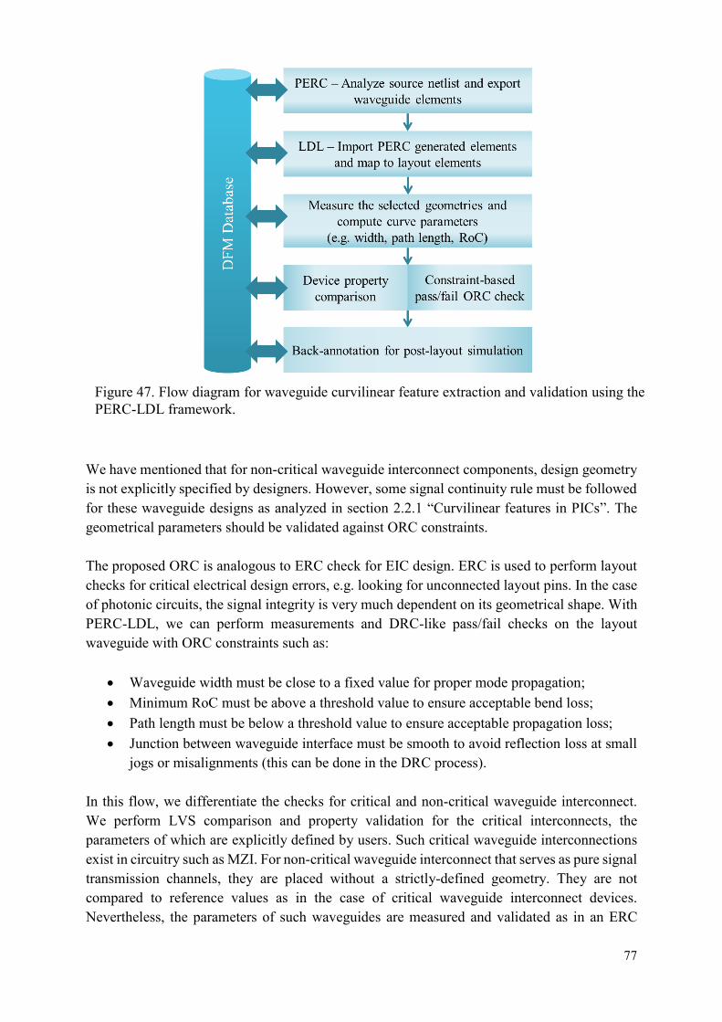
77
We have mentioned that for non-critical waveguide interconnect components, design geometry is not explicitly specified by designers. However, some signal continuity rule must be followed for these waveguide designs as analyzed in section 2.2.1 “Curvilinear features in PICs”. The geometrical parameters should be validated against ORC constraints. The proposed ORC is analogous to ERC check for EIC design. ERC is used to perform layout checks for critical electrical design errors, e.g. looking for unconnected layout pins. In the case of photonic circuits, the signal integrity is very much dependent on its geometrical shape. With PERC-LDL, we can perform measurements and DRC-like pass/fail checks on the layout waveguide with ORC constraints such as:
Waveguide width must be close to a fixed value for proper mode propagation; Minimum RoC must be above a threshold value to ensure acceptable bend loss; Path length must be below a threshold value to ensure acceptable propagation loss; Junction between waveguide interface must be smooth to avoid reflection loss at small
jogs or misalignments (this can be done in the DRC process). In this flow, we differentiate the checks for critical and non-critical waveguide interconnect. We perform LVS comparison and property validation for the critical interconnects, the parameters of which are explicitly defined by users. Such critical waveguide interconnections exist in circuitry such as MZI. For non-critical waveguide interconnect that serves as pure signal transmission channels, they are placed without a strictly-defined geometry. They are not compared to reference values as in the case of critical waveguide interconnect devices. Nevertheless, the parameters of such waveguides are measured and validated as in an ERC
Figure 47. Flow diagram for waveguide curvilinear feature extraction and validation using the PERC-LDL framework.
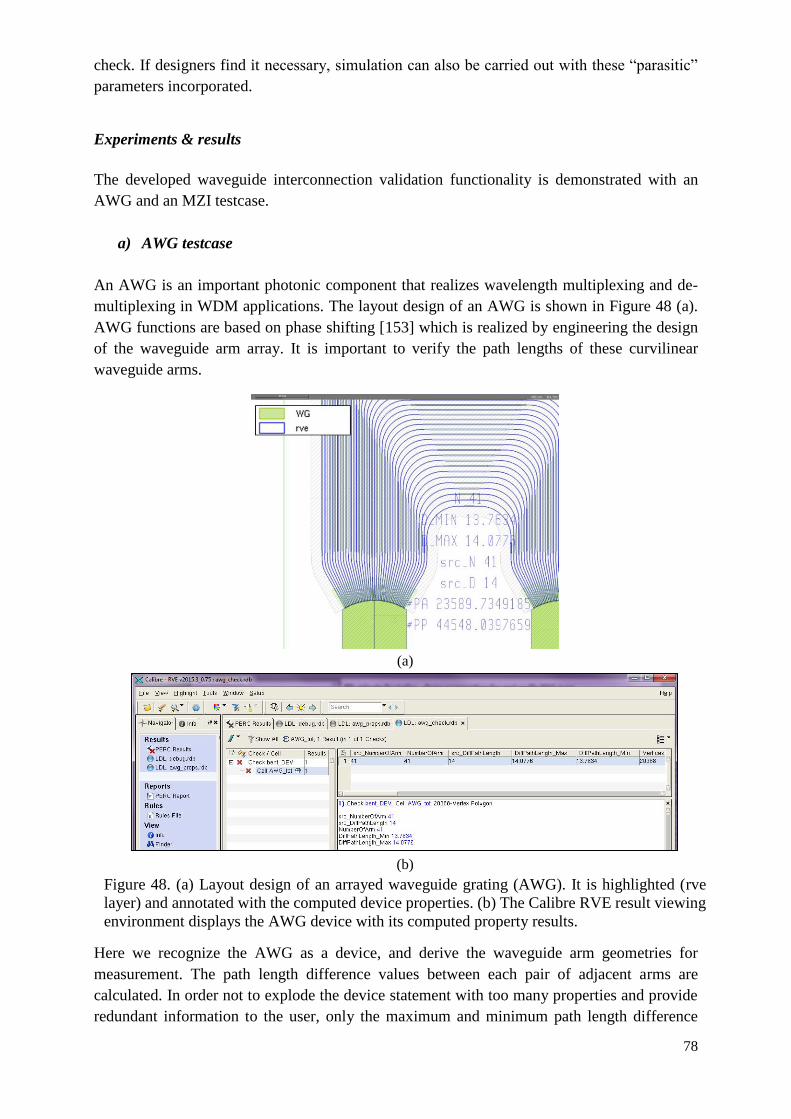
78
check. If designers find it necessary, simulation can also be carried out with these “parasitic”
parameters incorporated.
Experiments & results
The developed waveguide interconnection validation functionality is demonstrated with an
AWG and an MZI testcase.
a) AWG testcase
An AWG is an important photonic component that realizes wavelength multiplexing and de-
multiplexing in WDM applications. The layout design of an AWG is shown in Figure 48 (a).
AWG functions are based on phase shifting [153] which is realized by engineering the design
of the waveguide arm array. It is important to verify the path lengths of these curvilinear
waveguide arms.
Here we recognize the AWG as a device, and derive the waveguide arm geometries for
measurement. The path length difference values between each pair of adjacent arms are
calculated. In order not to explode the device statement with too many properties and provide
redundant information to the user, only the maximum and minimum path length difference
(a)
(b)
Figure 48. (a) Layout design of an arrayed waveguide grating (AWG). It is highlighted (rve
layer) and annotated with the computed device properties. (b) The Calibre RVE result viewing
environment displays the AWG device with its computed property results.

79
values are sorted and annotated as properties to the device. The extraction result is shown in
Figure 48 (b). 𝒔𝒓𝒄_𝑵𝒖𝒎𝒃𝒆𝒓𝑶𝒇𝑨𝒓𝒎 and 𝑵𝒖𝒎𝒃𝒆𝒓𝑶𝒇𝑨𝒓𝒎 are the source and layout
extracted number of arms respectively; 𝒔𝒓𝒄_𝑫𝒊𝒇𝒇𝑷𝒂𝒕𝒉𝑳𝒆𝒏𝒈𝒕𝒉, 𝑫𝒊𝒇𝒇𝑷𝒂𝒕𝒉𝑳𝒆𝒏𝒈𝒕𝒉_𝑴𝒂𝒙
and 𝑫𝒊𝒇𝒇𝑷𝒂𝒕𝒉𝑳𝒆𝒏𝒈𝒕𝒉_𝑴𝒊𝒏 are the source and layout extracted maximum and minimum path
length difference values respectively. These property values are highlighted on the layout as
layer “rve” in Figure 48 (a). The source and extracted values are compared. If a discrepancy
outside of the tolerance bound is found, an error will be reported.
In this case, AWG is a device with complex design geometries. We apply the waveguide
interconnect validation method on the waveguide arms. However, we will see that the validation
of devices by property comparison is limited to validate the entire AWG device, although it
may suffice for the relatively simple design of the waveguide arms which can be represented
by several parameters like width, length and curvature. As discussed in section 2.2.6 “Device
parameter comparison”, a shape-matching based method should be employed to validate such
device designs and will be discussed later.
b) MZI testcase
A MZI circuit is a widely used photonic component to realize signal modulation and can be
found in applications such as signal encoding/decoding, and bio-sensing. The device also
functions based on the engineered optical phase in the two MZI waveguide arms [154]. The
layout of an MZI circuit design is shown in Figure 49. Designers place these devices to build
an MZI by specifying exactly how the path is routed. The path is composed of a series of bends
and straight waveguides as individual devices, which are available from the PDK library.
Measurement results are shown on the layer “rve” and in the result viewing window in Figure
50. 𝒔𝒓𝒄_𝑳 and 𝑳 are the source and layout extracted path length values respectively; 𝒔𝒓𝒄_𝑹, 𝑹𝟏,
(a)
(b)
Figure 49. (a) Layout design of a Mach-Zehnder Interferometer (MZI) circuit. The two MZI
arms are highlighted on layer “rve” and annotated with computed properties. (b) The Calibre
RVE result viewing environment window displays the measurement results.
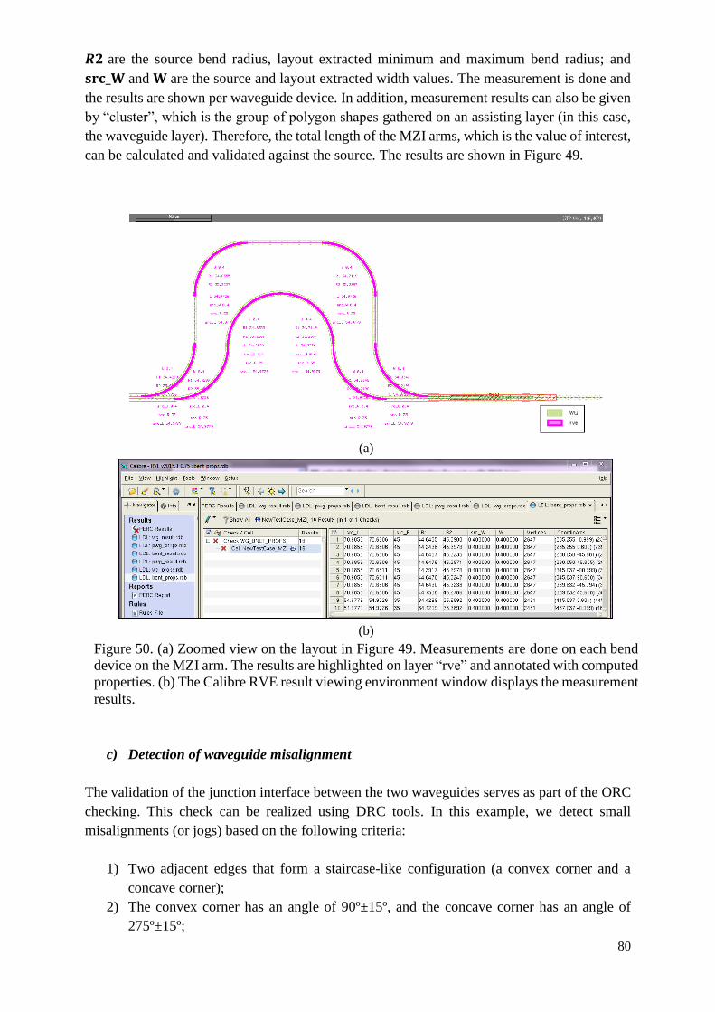
80
𝑹𝟐 are the source bend radius, layout extracted minimum and maximum bend radius; and
𝐬𝐫𝐜_𝐖 and 𝐖 are the source and layout extracted width values. The measurement is done and
the results are shown per waveguide device. In addition, measurement results can also be given
by “cluster”, which is the group of polygon shapes gathered on an assisting layer (in this case,
the waveguide layer). Therefore, the total length of the MZI arms, which is the value of interest,
can be calculated and validated against the source. The results are shown in Figure 49.
c) Detection of waveguide misalignment
The validation of the junction interface between the two waveguides serves as part of the ORC
checking. This check can be realized using DRC tools. In this example, we detect small
misalignments (or jogs) based on the following criteria:
1) Two adjacent edges that form a staircase-like configuration (a convex corner and a
concave corner);
2) The convex corner has an angle of 90º±15º, and the concave corner has an angle of
275º±15º;
(a)
(b)
Figure 50. (a) Zoomed view on the layout in Figure 49. Measurements are done on each bend
device on the MZI arm. The results are highlighted on layer “rve” and annotated with computed
properties. (b) The Calibre RVE result viewing environment window displays the measurement
results.
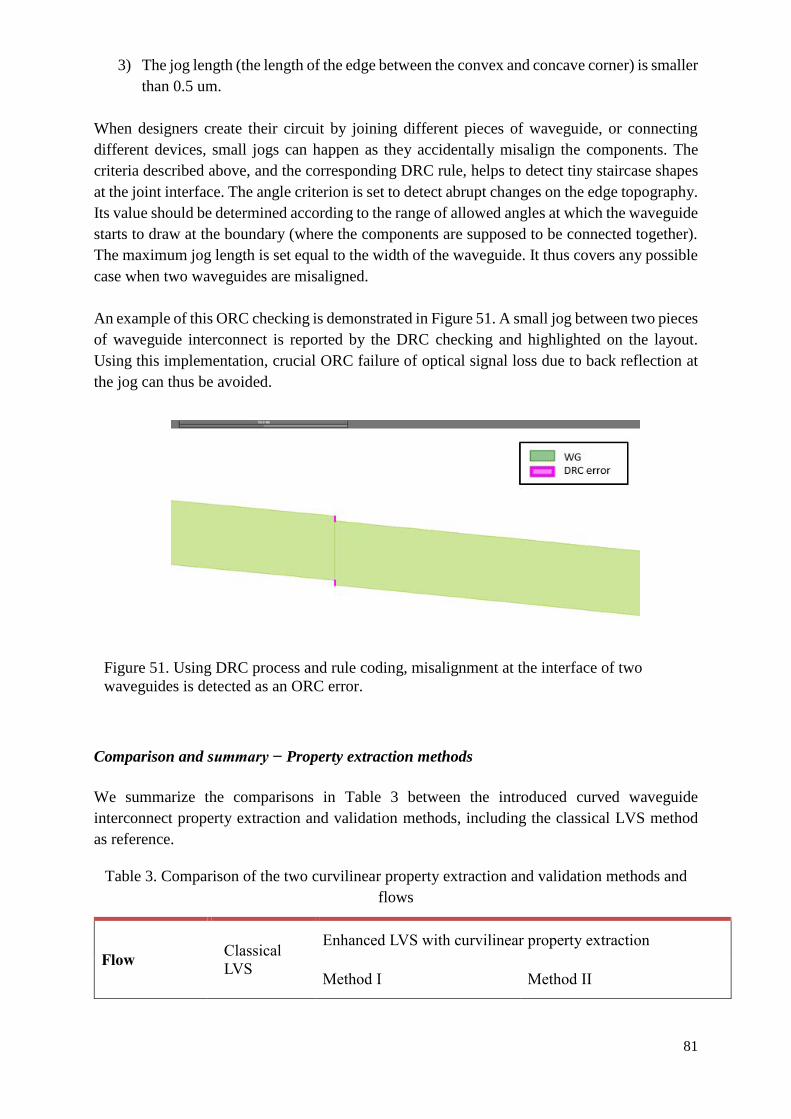
81
3) The jog length (the length of the edge between the convex and concave corner) is smaller
than 0.5 um.
When designers create their circuit by joining different pieces of waveguide, or connecting
different devices, small jogs can happen as they accidentally misalign the components. The
criteria described above, and the corresponding DRC rule, helps to detect tiny staircase shapes
at the joint interface. The angle criterion is set to detect abrupt changes on the edge topography.
Its value should be determined according to the range of allowed angles at which the waveguide
starts to draw at the boundary (where the components are supposed to be connected together).
The maximum jog length is set equal to the width of the waveguide. It thus covers any possible
case when two waveguides are misaligned.
An example of this ORC checking is demonstrated in Figure 51. A small jog between two pieces
of waveguide interconnect is reported by the DRC checking and highlighted on the layout.
Using this implementation, crucial ORC failure of optical signal loss due to back reflection at
the jog can thus be avoided.
Comparison and summary − Property extraction methods
We summarize the comparisons in Table 3 between the introduced curved waveguide
interconnect property extraction and validation methods, including the classical LVS method
as reference.
Table 3. Comparison of the two curvilinear property extraction and validation methods and
flows
Flow Classical
LVS
Enhanced LVS with curvilinear property extraction
Method I Method II
Figure 51. Using DRC process and rule coding, misalignment at the interface of two
waveguides is detected as an ORC error.
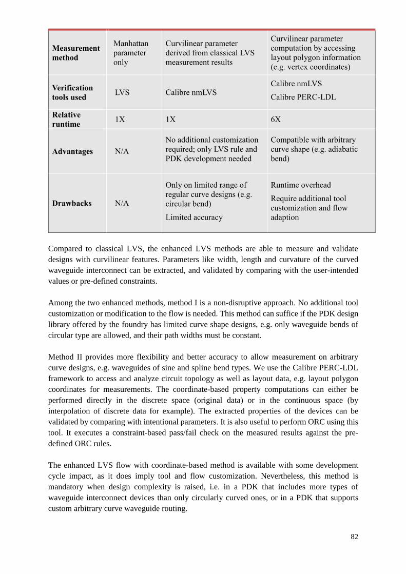
82
Measurement
method
Manhattan
parameter
only
Curvilinear parameter
derived from classical LVS
measurement results
Curvilinear parameter
computation by accessing
layout polygon information
(e.g. vertex coordinates)
Verification
tools used LVS Calibre nmLVS
Calibre nmLVS
Calibre PERC-LDL
Relative
runtime 1X 1X 6X
Advantages N/A
No additional customization
required; only LVS rule and
PDK development needed
Compatible with arbitrary
curve shape (e.g. adiabatic
bend)
Drawbacks N/A
Only on limited range of
regular curve designs (e.g.
circular bend)
Limited accuracy
Runtime overhead
Require additional tool
customization and flow
adaption
Compared to classical LVS, the enhanced LVS methods are able to measure and validate
designs with curvilinear features. Parameters like width, length and curvature of the curved
waveguide interconnect can be extracted, and validated by comparing with the user-intended
values or pre-defined constraints.
Among the two enhanced methods, method I is a non-disruptive approach. No additional tool
customization or modification to the flow is needed. This method can suffice if the PDK design
library offered by the foundry has limited curve shape designs, e.g. only waveguide bends of
circular type are allowed, and their path widths must be constant.
Method II provides more flexibility and better accuracy to allow measurement on arbitrary
curve designs, e.g. waveguides of sine and spline bend types. We use the Calibre PERC-LDL
framework to access and analyze circuit topology as well as layout data, e.g. layout polygon
coordinates for measurements. The coordinate-based property computations can either be
performed directly in the discrete space (original data) or in the continuous space (by
interpolation of discrete data for example). The extracted properties of the devices can be
validated by comparing with intentional parameters. It is also useful to perform ORC using this
tool. It executes a constraint-based pass/fail check on the measured results against the pre-
defined ORC rules.
The enhanced LVS flow with coordinate-based method is available with some development
cycle impact, as it does imply tool and flow customization. Nevertheless, this method is
mandatory when design complexity is raised, i.e. in a PDK that includes more types of
waveguide interconnect devices than only circularly curved ones, or in a PDK that supports
custom arbitrary curve waveguide routing.
83
4.3 Photonic Device Validation
Due to the fact that classical LVS is limited to handle curvilinear photonic device designs, the
black-box LVS is recommended as a primitive verification to perform basic circuit topology
validation when there is no proper method in place. Using foundry provided pre-characterized
cells which are CBC (correct-by-construction) effectively increases the chance of successful
design; however, device validation is nevertheless mandatory to verify if there is any undesired
modification that has been made to the cell when it is placed into the circuit context.
The methods and flows introduced in section 4.2 “Waveguide Interconnect Validation” are
responsible for verifying layout waveguide interconnect components. We have developed
advanced capability based on traditional PV tools to verify components with curvilinear features.
This is equally applicable to verify the layout of photonic devices that involve curvilinear
features. However, due to the complex device topologies and sensitivity to surrounding
structures, photonic devices cannot be easily characterized with a set of parameters (see section
2.2.6 “Device parameter comparison”). Device validation can be unreliable by performing
device parameter comparison. Therefore, instead of characterizing devices with parameters, we
alternatively recognize devices from a set of known patterns, including both the primary device
features and the surrounding "halo" of layout shapes.
In this flow, the pattern or the signature of pre-characterized devices are generated as the golden
design to be matched with layout devices. The pre-characterized devices are developed with the
help of existing silicon photonics simulators and are provided by component designers or by
foundries. If necessary, a small number of degrees of variability are introduced into the pattern,
but for the most part, the device in the layout must match one of the pre-characterized patterns
exactly. When the designer implements these pre-characterized devices in the layout, the LVS
tool can extract the device, measure its important parameters, and compare them to the pre-
characterized pattern. Any device that is not found in the pattern library is flagged as an
unknown device and considered a layout error. These methods will be discussed in section 4.3.2
“Fixed cell in-context validation”.
The above approach introduces a strict limitation: each device instantiated into the layout must
match an exact expected layout pattern. The preference is to enable a similar recognition based
on pre-characterized devices which may vary in a set of known parameters. This can only be
achieved with some way to pass the intended device shape, for each placement, to the
verification system. This is possible through design tool and flow integrations, and it will be
discussed in detail in section 4.3.3 “Parameterized cell in-context validation”. Given the ability
to compare the intended structure to the layout, and knowing the original parameters used to
generate such a structure, and once the component shape has been verified as meeting
expectations, it is no longer necessary to physically re-extract the parameters. Instead, the
original parameters used when placing the structure can be passed back out to the extracted
layout. The original parameters may be passed to LVS in the form of text in the layout
associated to the specific device or structure, or through other formats passed to the LVS flow.
84
4.3.1 Device Context Detection
To ensure that the pre-characterized device is not modified by unintended interaction with other
design structures in the layout during its placement, it is possible to perform a DRC-like check
for this purpose. Such a check is coded as:
The above code detects any discrepancy between the waveguide geometries inside the device
cell and the ones within the device extent (i.e. the bounding area around the device, which can
be user-defined) and interacting with the device waveguide. In this way, pre-characterized
devices are ensured to be unmodified when placed into the circuit context.
This method does not require building a golden design library to perform matching of the golden
device design versus a layout placed device. Instead, it detects if the placed device interferes
with geometries in the context of the design. The drawback of this method is that it does not
report interaction of two identical cells that are overlapped. Designers can also accidentally
modify the device cell content, which cannot be detected using this method.
4.3.2 Fixed cell in-context validation
The previously mentioned device context detection method is fast and easy to implement. In
this section, we will introduce alternative methods that find the exact match of the device design
intent with that placed into the circuit layout context.
a) Cell geometry equivalence DRC check
If the foundry pre-characterized device is proved to be unchanged when designers place them
into the circuit context, we can safely say that the device functions as intended. Possible
deviation from the intent is detected by geometrical equivalence comparison checks between
the golden device design and the placed design. Using the DRC utility such as that offered by
Calibre DRC, such a geometry comparison check can be performed. The workflow diagram is
drawn in Figure 52. First, a layout with a golden device design should be created. On the
implementation side, designers create the circuit layout by place and route of the pre-
characterized devices into a circuit. Then the DRC cell identification and geometrical
comparison flow is called to perform device validation. The corresponding layout cell and
golden cell to be compared are specified by their cell names. The two cell geometries are
compared. The comparison returns a pass/fail result: the validation passes if the layout device
is identical to the golden device design; otherwise, the tool reports an error, indicating the
deviation of the layout placed device from the original device design intent.
𝑑𝑒𝑣𝑖𝑐𝑒𝑊𝐺 ∶= 𝑤𝑎𝑣𝑒𝑔𝑢𝑖𝑑𝑒 𝑙𝑎𝑦𝑒𝑟 𝑔𝑒𝑜𝑚𝑒𝑡𝑟𝑖𝑒𝑠 𝑖𝑛𝑠𝑖𝑑𝑒 𝑡ℎ𝑒 𝑑𝑒𝑣𝑖𝑐𝑒 𝑐𝑒𝑙𝑙
𝑖𝑛𝐶𝑜𝑛𝑡𝑒𝑥𝑡𝐷𝑒𝑣𝑖𝑐𝑒𝑊𝐺 ≔
𝑤𝑎𝑣𝑒𝑔𝑢𝑖𝑑𝑒 𝑔𝑒𝑜𝑚𝑒𝑡𝑟𝑖𝑒𝑠 𝑖𝑛𝑠𝑖𝑑𝑒 𝑑𝑒𝑣𝑖𝑐𝑒 𝑒𝑥𝑡𝑒𝑛𝑡 𝑡ℎ𝑎𝑡 𝑖𝑛𝑡𝑒𝑟𝑎𝑐𝑡 𝑤𝑖𝑡ℎ 𝑑𝑒𝑣𝑖𝑐𝑒𝑊𝐺
𝐸𝑟𝑟𝑜𝑟 ≔ 𝑖𝑛𝐶𝑜𝑛𝑡𝑒𝑥𝑡𝐷𝑒𝑣𝑖𝑐𝑒𝑊𝐺 − 𝑑𝑒𝑣𝑖𝑐𝑒𝑊𝐺
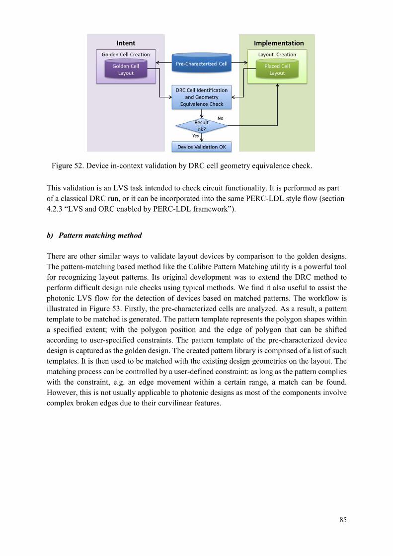
85
This validation is an LVS task intended to check circuit functionality. It is performed as part of a classical DRC run, or it can be incorporated into the same PERC-LDL style flow (section 4.2.3 “LVS and ORC enabled by PERC-LDL framework”).
b) Pattern matching method There are other similar ways to validate layout devices by comparison to the golden designs. The pattern-matching based method like the Calibre Pattern Matching utility is a powerful tool for recognizing layout patterns. Its original development was to extend the DRC method to perform difficult design rule checks using typical methods. We find it also useful to assist the photonic LVS flow for the detection of devices based on matched patterns. The workflow is illustrated in Figure 53. Firstly, the pre-characterized cells are analyzed. As a result, a pattern template to be matched is generated. The pattern template represents the polygon shapes within a specified extent; with the polygon position and the edge of polygon that can be shifted according to user-specified constraints. The pattern template of the pre-characterized device design is captured as the golden design. The created pattern library is comprised of a list of such templates. It is then used to be matched with the existing design geometries on the layout. The matching process can be controlled by a user-defined constraint: as long as the pattern complies with the constraint, e.g. an edge movement within a certain range, a match can be found. However, this is not usually applicable to photonic designs as most of the components involve complex broken edges due to their curvilinear features.
Figure 52. Device in-context validation by DRC cell geometry equivalence check.
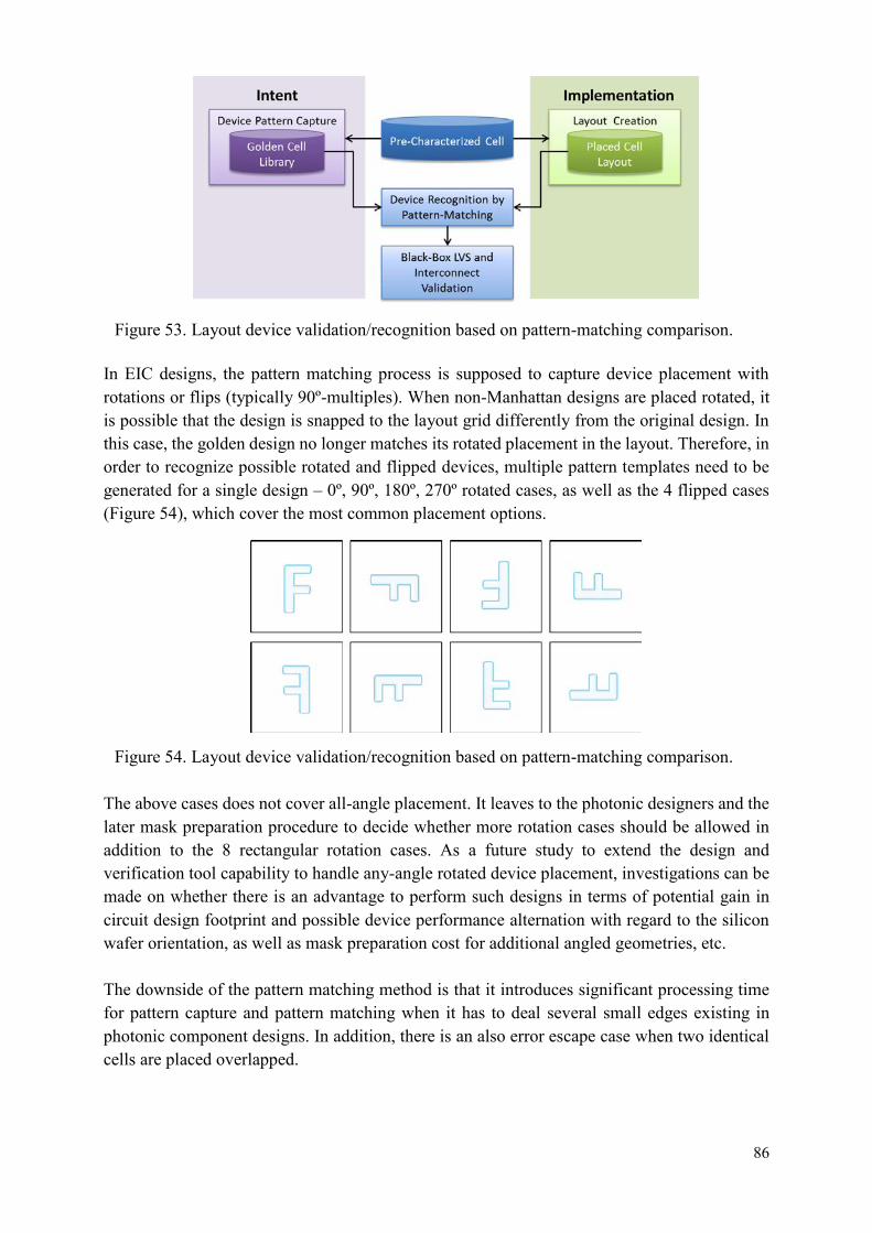
86
In EIC designs, the pattern matching process is supposed to capture device placement with rotations or flips (typically 90º-multiples). When non-Manhattan designs are placed rotated, it is possible that the design is snapped to the layout grid differently from the original design. In this case, the golden design no longer matches its rotated placement in the layout. Therefore, in order to recognize possible rotated and flipped devices, multiple pattern templates need to be generated for a single design – 0º, 90º, 180º, 270º rotated cases, as well as the 4 flipped cases (Figure 54), which cover the most common placement options.
The above cases does not cover all-angle placement. It leaves to the photonic designers and the later mask preparation procedure to decide whether more rotation cases should be allowed in addition to the 8 rectangular rotation cases. As a future study to extend the design and verification tool capability to handle any-angle rotated device placement, investigations can be made on whether there is an advantage to perform such designs in terms of potential gain in circuit design footprint and possible device performance alternation with regard to the silicon wafer orientation, as well as mask preparation cost for additional angled geometries, etc. The downside of the pattern matching method is that it introduces significant processing time for pattern capture and pattern matching when it has to deal several small edges existing in photonic component designs. In addition, there is an also error escape case when two identical cells are placed overlapped.
Figure 53. Layout device validation/recognition based on pattern-matching comparison.
Figure 54. Layout device validation/recognition based on pattern-matching comparison.
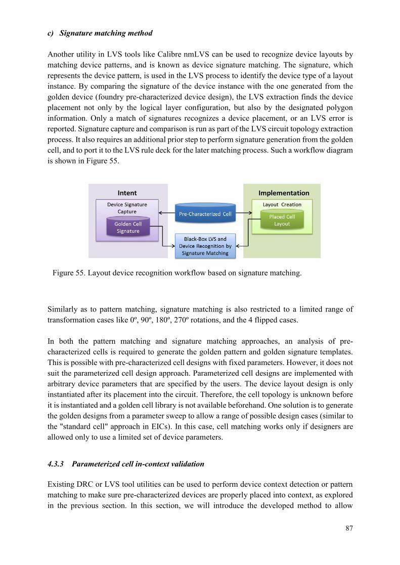
87
c) Signature matching method Another utility in LVS tools like Calibre nmLVS can be used to recognize device layouts by matching device patterns, and is known as device signature matching. The signature, which represents the device pattern, is used in the LVS process to identify the device type of a layout instance. By comparing the signature of the device instance with the one generated from the golden device (foundry pre-characterized device design), the LVS extraction finds the device placement not only by the logical layer configuration, but also by the designated polygon information. Only a match of signatures recognizes a device placement, or an LVS error is reported. Signature capture and comparison is run as part of the LVS circuit topology extraction process. It also requires an additional prior step to perform signature generation from the golden cell, and to port it to the LVS rule deck for the later matching process. Such a workflow diagram is shown in Figure 55.
Similarly as to pattern matching, signature matching is also restricted to a limited range of transformation cases like 0º, 90º, 180º, 270º rotations, and the 4 flipped cases. In both the pattern matching and signature matching approaches, an analysis of pre-characterized cells is required to generate the golden pattern and golden signature templates. This is possible with pre-characterized cell designs with fixed parameters. However, it does not suit the parameterized cell design approach. Parameterized cell designs are implemented with arbitrary device parameters that are specified by the users. The device layout design is only instantiated after its placement into the circuit. Therefore, the cell topology is unknown before it is instantiated and a golden cell library is not available beforehand. One solution is to generate the golden designs from a parameter sweep to allow a range of possible design cases (similar to the "standard cell" approach in EICs). In this case, cell matching works only if designers are allowed only to use a limited set of device parameters.
4.3.3 Parameterized cell in-context validation Existing DRC or LVS tool utilities can be used to perform device context detection or pattern matching to make sure pre-characterized devices are properly placed into context, as explored in the previous section. In this section, we will introduce the developed method to allow
Figure 55. Layout device recognition workflow based on signature matching.
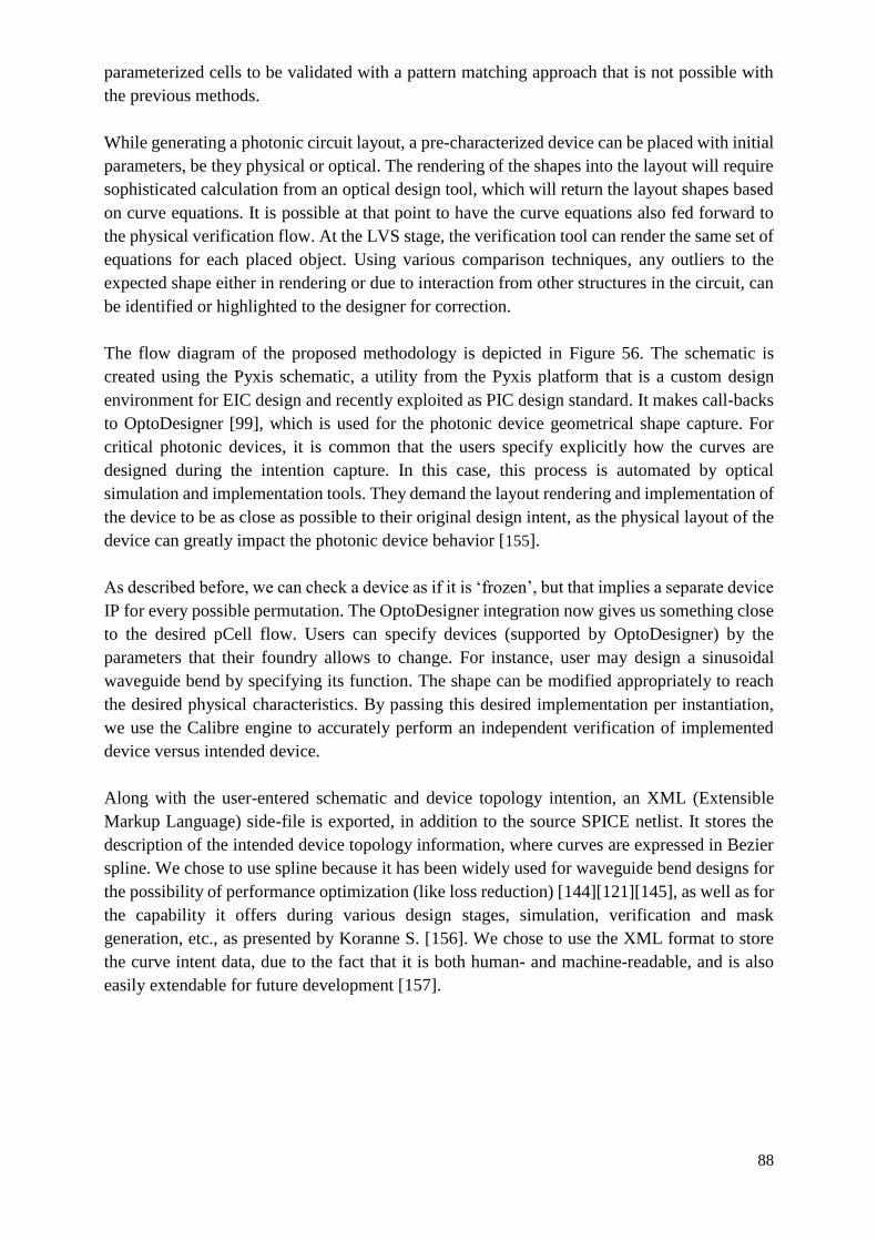
88
parameterized cells to be validated with a pattern matching approach that is not possible with
the previous methods.
While generating a photonic circuit layout, a pre-characterized device can be placed with initial
parameters, be they physical or optical. The rendering of the shapes into the layout will require
sophisticated calculation from an optical design tool, which will return the layout shapes based
on curve equations. It is possible at that point to have the curve equations also fed forward to
the physical verification flow. At the LVS stage, the verification tool can render the same set of
equations for each placed object. Using various comparison techniques, any outliers to the
expected shape either in rendering or due to interaction from other structures in the circuit, can
be identified or highlighted to the designer for correction.
The flow diagram of the proposed methodology is depicted in Figure 56. The schematic is
created using the Pyxis schematic, a utility from the Pyxis platform that is a custom design
environment for EIC design and recently exploited as PIC design standard. It makes call-backs
to OptoDesigner [99], which is used for the photonic device geometrical shape capture. For
critical photonic devices, it is common that the users specify explicitly how the curves are
designed during the intention capture. In this case, this process is automated by optical
simulation and implementation tools. They demand the layout rendering and implementation of
the device to be as close as possible to their original design intent, as the physical layout of the
device can greatly impact the photonic device behavior [155].
As described before, we can check a device as if it is ‘frozen’, but that implies a separate device
IP for every possible permutation. The OptoDesigner integration now gives us something close
to the desired pCell flow. Users can specify devices (supported by OptoDesigner) by the
parameters that their foundry allows to change. For instance, user may design a sinusoidal
waveguide bend by specifying its function. The shape can be modified appropriately to reach
the desired physical characteristics. By passing this desired implementation per instantiation,
we use the Calibre engine to accurately perform an independent verification of implemented
device versus intended device.
Along with the user-entered schematic and device topology intention, an XML (Extensible
Markup Language) side-file is exported, in addition to the source SPICE netlist. It stores the
description of the intended device topology information, where curves are expressed in Bezier
spline. We chose to use spline because it has been widely used for waveguide bend designs for
the possibility of performance optimization (like loss reduction) [144][121][145], as well as for
the capability it offers during various design stages, simulation, verification and mask
generation, etc., as presented by Koranne S. [156]. We chose to use the XML format to store
the curve intent data, due to the fact that it is both human- and machine-readable, and is also
easily extendable for future development [157].

89
The layout is implemented by editors such as Pyxis Layout. Next, on the DRC-clean layout, a classical LVS comparison is performed. After the first-phase black-box LVS passes, “shape-matching comparison” is performed to validate the instantiated pCell device. The XML file is
first parsed using the TclXML package [158] in order to read various design intent data. Such data includes the sets of cubic Bezier curve parameters that represent the curve central path; the width which is used to compute the envelop of the path; and the transformation function which is used to determine the location and rotation of the shape. The cubic Bezier curve is defined as:
𝑷(𝑡) = (1 − 𝑡)3𝒂𝟎 + 3(1 − 𝑡)2𝑡𝒂𝟏 + 3(1 − 𝑡)𝑡2𝒂𝟐 + 𝑡3𝒂𝟑 , 0 ≤ 𝑡 ≤ 1. Where Bezier curve 𝑷 is expressed with a combination of control points 𝒂𝟎, 𝒂𝟏, 𝒂𝟐, 𝒂𝟑 with time-varying coefficients. The transformation matrix is defined as:
[M] = [𝑚11 𝑚12 𝑚13𝑚21 𝑚22 𝑚23𝑚31 𝑚32 𝑚33
]
An example the source file is shown as followed:
Figure 56. Flow diagram of pCell device validation by shape-matching method.
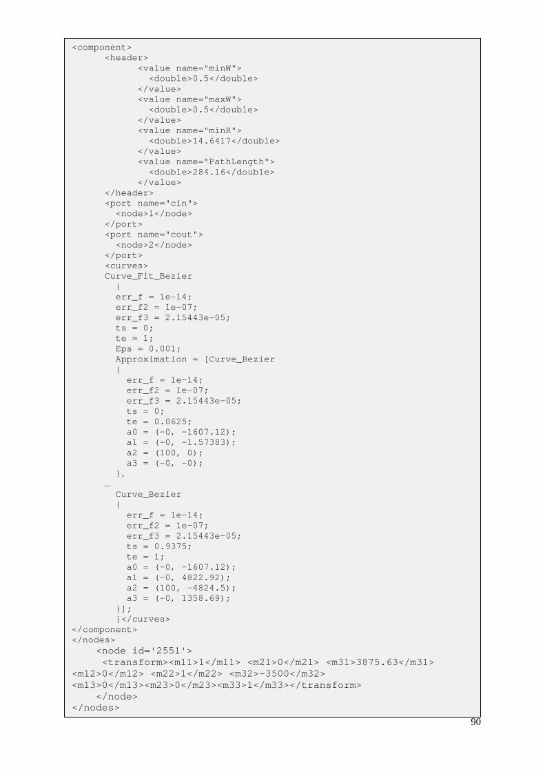
90
<component>
<header>
<value name="minW">
<double>0.5</double>
</value>
<value name="maxW">
<double>0.5</double>
</value>
<value name="minR">
<double>14.6417</double>
</value>
<value name="PathLength">
<double>284.16</double>
</value>
</header>
<port name="cin">
<node>1</node>
</port>
<port name="cout">
<node>2</node>
</port>
<curves>
Curve_Fit_Bezier
{
err_f = 1e-14;
err_f2 = 1e-07;
err_f3 = 2.15443e-05;
ts = 0;
te = 1;
Eps = 0.001;
Approximation = [Curve_Bezier
{
err_f = 1e-14;
err_f2 = 1e-07;
err_f3 = 2.15443e-05;
ts = 0;
te = 0.0625;
a0 = (-0, -1607.12);
a1 = (-0, -1.57383);
a2 = (100, 0);
a3 = (-0, -0);
},
…
Curve_Bezier
{
err_f = 1e-14;
err_f2 = 1e-07;
err_f3 = 2.15443e-05;
ts = 0.9375;
te = 1;
a0 = (-0, -1607.12);
a1 = (-0, 4822.92);
a2 = (100, -4824.5);
a3 = (-0, 1358.69);
}];
}</curves>
</component>
</nodes>
<node id='2551'>
<transform><m11>1</m11> <m21>0</m21> <m31>3875.63</m31>
<m12>0</m12> <m22>1</m22> <m32>-3500</m32>
<m13>0</m13><m23>0</m23><m33>1</m33></transform>
</node>
</nodes>
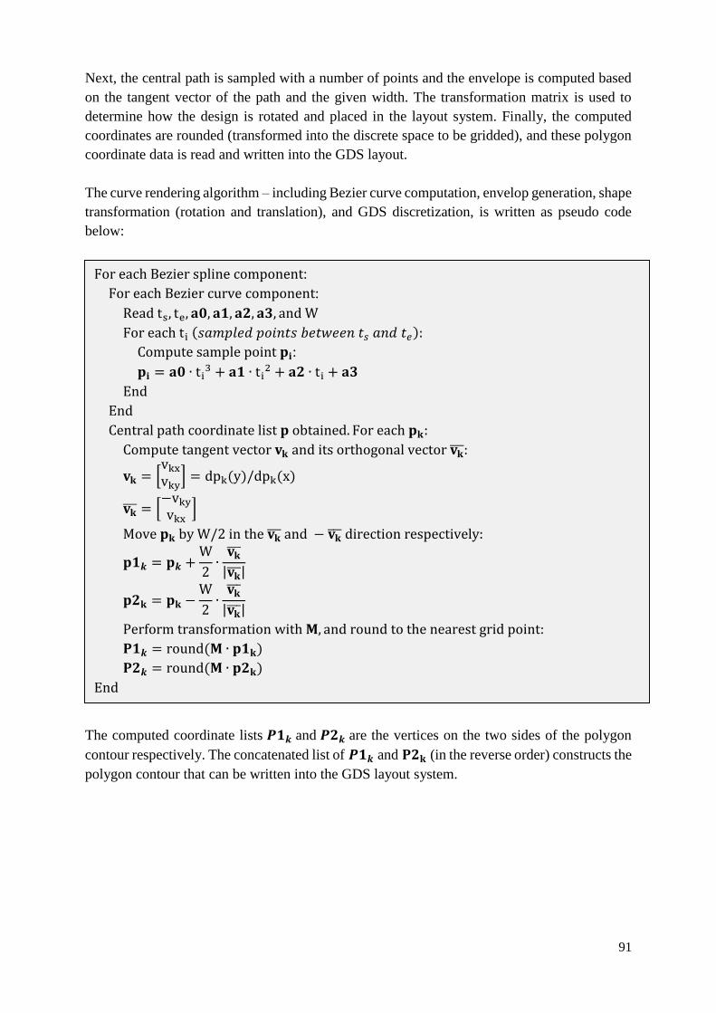
91
Next, the central path is sampled with a number of points and the envelope is computed based
on the tangent vector of the path and the given width. The transformation matrix is used to
determine how the design is rotated and placed in the layout system. Finally, the computed
coordinates are rounded (transformed into the discrete space to be gridded), and these polygon
coordinate data is read and written into the GDS layout.
The curve rendering algorithm – including Bezier curve computation, envelop generation, shape
transformation (rotation and translation), and GDS discretization, is written as pseudo code
below:
The computed coordinate lists 𝑷𝟏𝒌 and 𝑷𝟐𝒌 are the vertices on the two sides of the polygon
contour respectively. The concatenated list of 𝑷𝟏𝒌 and 𝐏𝟐𝐤 (in the reverse order) constructs the
polygon contour that can be written into the GDS layout system.
For each Bezier spline component:
For each Bezier curve component:
Read ts, te, 𝐚𝟎, 𝐚𝟏, 𝐚𝟐, 𝐚𝟑, and W
For each ti (𝑠𝑎𝑚𝑝𝑙𝑒𝑑 𝑝𝑜𝑖𝑛𝑡𝑠 𝑏𝑒𝑡𝑤𝑒𝑒𝑛 𝑡𝑠 𝑎𝑛𝑑 𝑡𝑒):
Compute sample point 𝐩𝐢:
𝐩𝐢 = 𝐚𝟎 ∙ ti3 + 𝐚𝟏 ∙ ti
2 + 𝐚𝟐 ∙ ti + 𝐚𝟑
End
End
Central path coordinate list 𝐩 obtained. For each 𝐩𝐤:
Compute tangent vector 𝐯𝐤 and its orthogonal vector 𝐯𝐤̅̅ ̅:
𝐯𝐤 = [vkx
vky] = dpk(y)/dpk(x)
𝐯𝐤̅̅ ̅ = [−vky
vkx]
Move 𝐩𝐤 by W/2 in the 𝐯𝐤̅̅ ̅ and − 𝐯𝐤̅̅ ̅ direction respectively:
𝐩𝟏𝒌 = 𝐩𝒌 +W
2∙
𝐯𝐤̅̅ ̅
|𝐯𝐤̅̅ ̅|
𝐩𝟐𝐤 = 𝐩𝐤 −W
2∙
𝐯𝐤̅̅ ̅
|𝐯𝐤̅̅ ̅|
Perform transformation with 𝐌, and round to the nearest grid point:
𝐏𝟏𝒌 = round(𝐌 ∙ 𝐩𝟏𝐤)
𝐏𝟐𝒌 = round(𝐌 ∙ 𝐩𝟐𝐤)
End
92
After the reference design is created, it is compared with the drawn design layout, as depicted in Figure 57. The discrepancy between the two is found by performing a Boolean XOR operation, which is the "exclusive or" logical operation that outputs true only when both inputs differ. A tolerance of (√2 ∙ 𝑔𝑟𝑖𝑑_𝑠𝑖𝑧𝑒) is applied to filter the discrepancy result. This is to compensate the rounding which is applied when computing the polygon envelope. An XOR shape comparison example is shown in Figure 58. The outlier of the drawn layout from the reference is found and is output as an error result.
Figure 57. Layout reference design creation from the XML side-file input.
93
The output of the flow is a pass/fail result: if a discrepancy exists or not. If so, it is flagged on the layout and requires corrections. For the purpose of post-layout simulation, certain device parameters should be passed on. The source netlist is annotated beforehand with the requested parameters for simulation. Because the geometric verification has confirmed that the layout design is done correctly, we safely pass those parameters from the source netlist to the post-layout simulation (as depicted in flow diagram Figure 56).
Experiments & result A demonstration is shown on a photonic circuit example, which is built based on the generic demo PDK provided by PhoeniX Software. The schematic design is entered using OptoDesigner, along with a SPICE netlist and a generated XML side-file. The parameterized
Figure 58. Validation of layout placed device against the reference device design: a) the reference device design; b) the layout placed device; c) discrepancy between the two data is found by the XOR Boolean operation; d) the discrepancy result is highlighted as error.
a) b) c) d)
94
waveguide components to be validated are exported with feature information annotated in this XML file. The information includes the component name, the Bezier spline parameters of the geometry central path, width, location and rotation of the component. An example of the used XML file is shown below:
After the schematic is created, we implement the layout using editors such as Pyxis Layout. The created layout is as shown in Figure 60.
Then, black-box LVS is carried out to check the basic circuit topology. Next, we make use of the programmable interface of a design tool, like Calibre DESIGNrev, in order to parse the XML file and transform it into the layout (a similar functionality is also possible with the Calibre PERC-LDL framework); the available information in the file allows DESIGNrev to reconstruct and render the reference design geometries onto the same layout file (the created geometries are highlighted in Figure 60); with the reference and layout design on the same layout, they are compared by the XOR operation; finally, the discrepancy result is reported as error result which indicates that the layout implementation of the device is incorrect – different from the design intent, and it requires correction.
<?xml version=”1.0”?> <component> <name> DeviceName </name> <bezier> BezierSplineParameters </bezier> <width> Width </width> <transformation> TransformationMatrix </transformation> </component>
Figure 59. Layout design of a photonic circuit based on a generic PDK provided by PhoeniX Software.
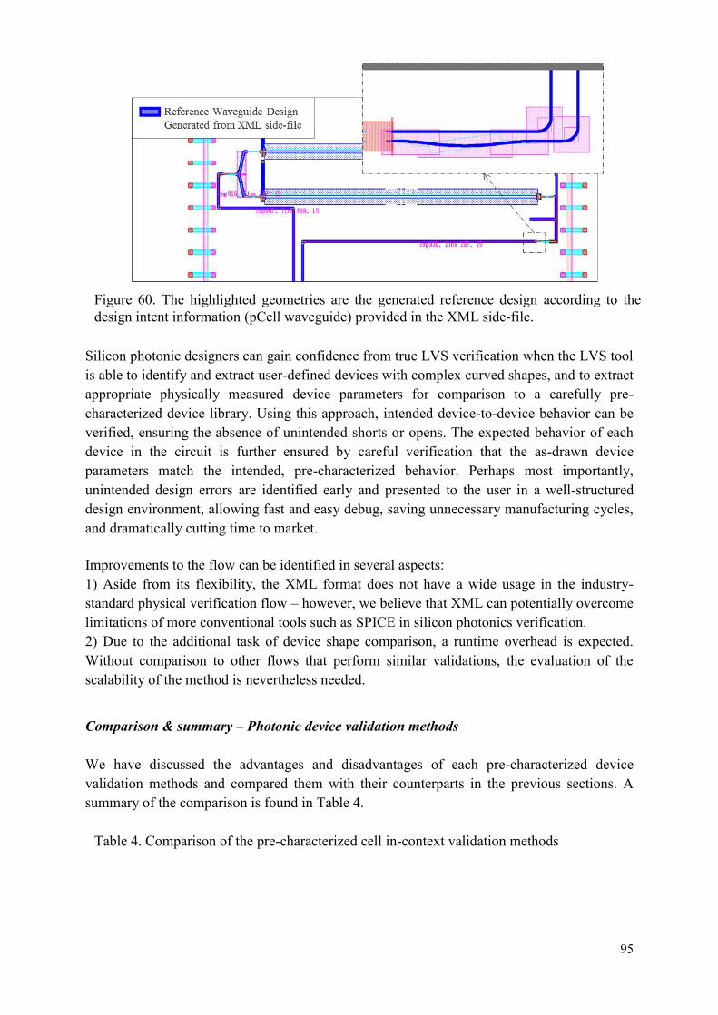
95
Silicon photonic designers can gain confidence from true LVS verification when the LVS tool is able to identify and extract user-defined devices with complex curved shapes, and to extract appropriate physically measured device parameters for comparison to a carefully pre-characterized device library. Using this approach, intended device-to-device behavior can be verified, ensuring the absence of unintended shorts or opens. The expected behavior of each device in the circuit is further ensured by careful verification that the as-drawn device parameters match the intended, pre-characterized behavior. Perhaps most importantly, unintended design errors are identified early and presented to the user in a well-structured design environment, allowing fast and easy debug, saving unnecessary manufacturing cycles, and dramatically cutting time to market. Improvements to the flow can be identified in several aspects: 1) Aside from its flexibility, the XML format does not have a wide usage in the industry-standard physical verification flow – however, we believe that XML can potentially overcome limitations of more conventional tools such as SPICE in silicon photonics verification. 2) Due to the additional task of device shape comparison, a runtime overhead is expected. Without comparison to other flows that perform similar validations, the evaluation of the scalability of the method is nevertheless needed.
Comparison & summary – Photonic device validation methods We have discussed the advantages and disadvantages of each pre-characterized device validation methods and compared them with their counterparts in the previous sections. A summary of the comparison is found in Table 4.
Figure 60. The highlighted geometries are the generated reference design according to the design intent information (pCell waveguide) provided in the XML side-file.
Table 4. Comparison of the pre-characterized cell in-context validation methods
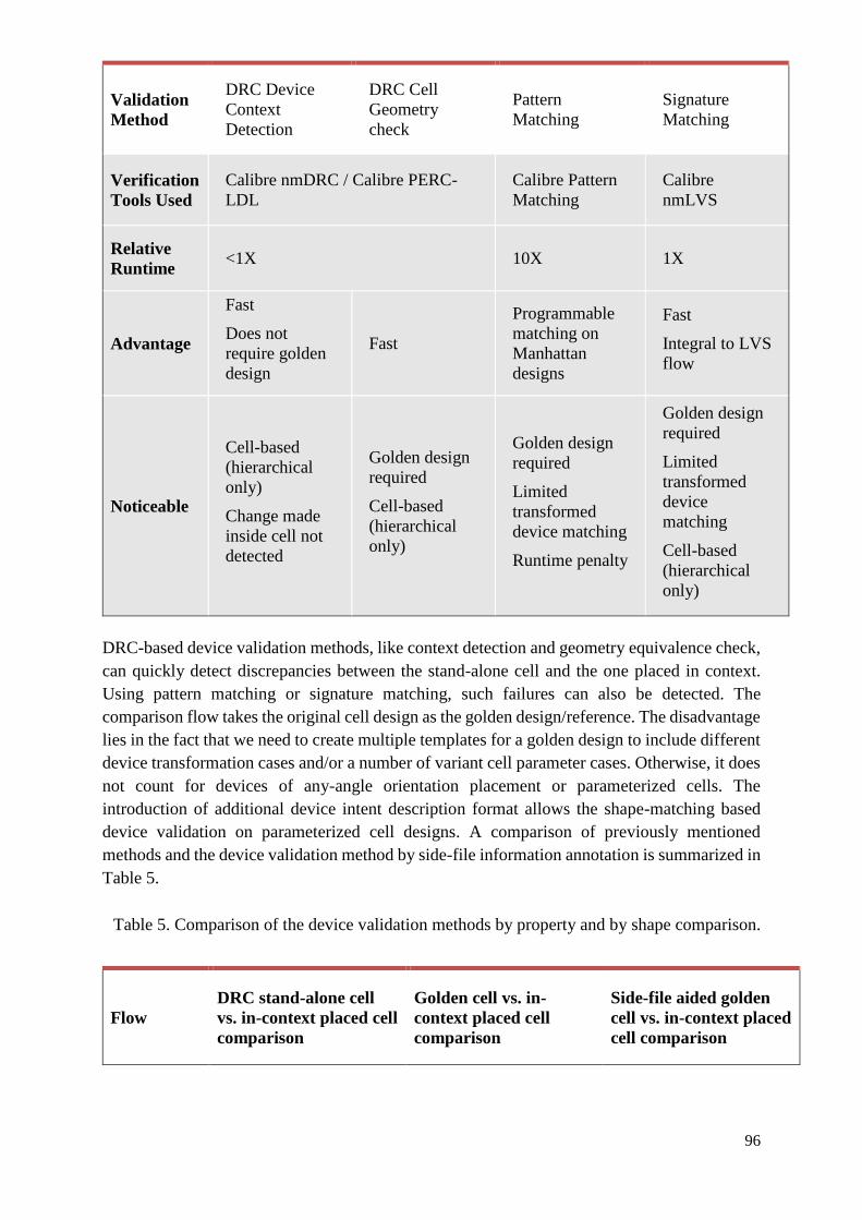
96
Validation
Method
DRC Device
Context
Detection
DRC Cell
Geometry
check
Pattern
Matching
Signature
Matching
Verification
Tools Used
Calibre nmDRC / Calibre PERC-
LDL
Calibre Pattern
Matching
Calibre
nmLVS
Relative
Runtime <1X 10X 1X
Advantage
Fast
Does not
require golden
design
Fast
Programmable
matching on
Manhattan
designs
Fast
Integral to LVS
flow
Noticeable
Cell-based
(hierarchical
only)
Change made
inside cell not
detected
Golden design
required
Cell-based
(hierarchical
only)
Golden design
required
Limited
transformed
device matching
Runtime penalty
Golden design
required
Limited
transformed
device
matching
Cell-based
(hierarchical
only)
DRC-based device validation methods, like context detection and geometry equivalence check,
can quickly detect discrepancies between the stand-alone cell and the one placed in context.
Using pattern matching or signature matching, such failures can also be detected. The
comparison flow takes the original cell design as the golden design/reference. The disadvantage
lies in the fact that we need to create multiple templates for a golden design to include different
device transformation cases and/or a number of variant cell parameter cases. Otherwise, it does
not count for devices of any-angle orientation placement or parameterized cells. The
introduction of additional device intent description format allows the shape-matching based
device validation on parameterized cell designs. A comparison of previously mentioned
methods and the device validation method by side-file information annotation is summarized in
Table 5.
Flow
DRC stand-alone cell
vs. in-context placed cell
comparison
Golden cell vs. in-
context placed cell
comparison
Side-file aided golden
cell vs. in-context placed
cell comparison
Table 5. Comparison of the device validation methods by property and by shape comparison.
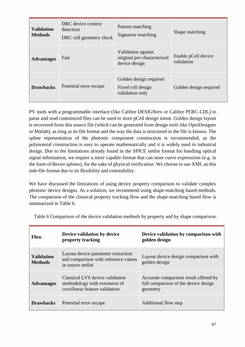
97
Validation
Methods
DRC device context
detection
DRC cell geometry check
Pattern matching
Signature matching Shape matching
Advantages Fast
Validation against
original pre-characterized
device design
Enable pCell device
validation
Drawbacks Potential error escape
Golden design required
Fixed cell design
validation only
Golden design required
PV tools with a programmable interface (like Calibre DESIGNrev or Calibre PERC-LDL) to
parse and read customized files can be used to store pCell design intent. Golden design layout
is recovered from this source file (which can be generated from design tools like OptoDesigner
or Matlab), as long as its file format and the way the data is structured in the file is known. The
spline representation of the photonic component construction is recommended, as the
polynomial construction is easy to operate mathematically and it is widely used in industrial
design. Due to the limitations already found in the SPICE netlist format for handling optical
signal information, we require a more capable format that can store curve expressions (e.g. in
the form of Bezier splines), for the sake of physical verification. We choose to use XML as this
side-file format due to its flexibility and extensibility.
We have discussed the limitations of using device property comparison to validate complex
photonic device designs. As a solution, we recommend using shape-matching based methods.
The comparison of the classical property tracking flow and the shape-matching based flow is
summarized in Table 6.
Flow Device validation by device
property tracking
Device validation by comparison with
golden design
Validation
Methods
Layout device parameter extraction
and comparison with reference values
in source netlist
Layout device design comparison with
golden design
Advantages
Classical LVS device validation
methodology with extension of
curvilinear feature validation
Accurate comparison result offered by
full comparison of the device design
geometry
Drawbacks Potential error escape Additional flow step
Table 6 Comparison of the device validation methods by property and by shape comparison.
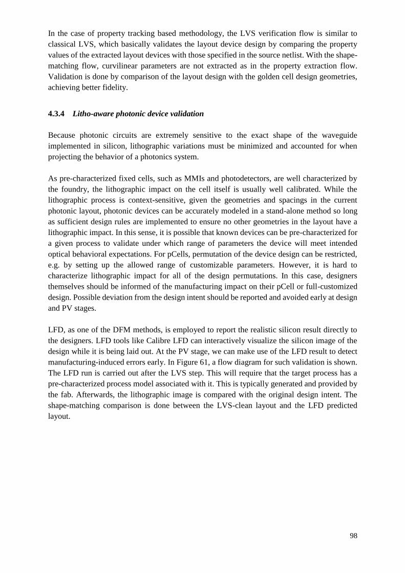
98
In the case of property tracking based methodology, the LVS verification flow is similar to
classical LVS, which basically validates the layout device design by comparing the property
values of the extracted layout devices with those specified in the source netlist. With the shape-
matching flow, curvilinear parameters are not extracted as in the property extraction flow.
Validation is done by comparison of the layout design with the golden cell design geometries,
achieving better fidelity.
4.3.4 Litho-aware photonic device validation
Because photonic circuits are extremely sensitive to the exact shape of the waveguide
implemented in silicon, lithographic variations must be minimized and accounted for when
projecting the behavior of a photonics system.
As pre-characterized fixed cells, such as MMIs and photodetectors, are well characterized by
the foundry, the lithographic impact on the cell itself is usually well calibrated. While the
lithographic process is context-sensitive, given the geometries and spacings in the current
photonic layout, photonic devices can be accurately modeled in a stand-alone method so long
as sufficient design rules are implemented to ensure no other geometries in the layout have a
lithographic impact. In this sense, it is possible that known devices can be pre-characterized for
a given process to validate under which range of parameters the device will meet intended
optical behavioral expectations. For pCells, permutation of the device design can be restricted,
e.g. by setting up the allowed range of customizable parameters. However, it is hard to
characterize lithographic impact for all of the design permutations. In this case, designers
themselves should be informed of the manufacturing impact on their pCell or full-customized
design. Possible deviation from the design intent should be reported and avoided early at design
and PV stages.
LFD, as one of the DFM methods, is employed to report the realistic silicon result directly to
the designers. LFD tools like Calibre LFD can interactively visualize the silicon image of the
design while it is being laid out. At the PV stage, we can make use of the LFD result to detect
manufacturing-induced errors early. In Figure 61, a flow diagram for such validation is shown.
The LFD run is carried out after the LVS step. This will require that the target process has a
pre-characterized process model associated with it. This is typically generated and provided by
the fab. Afterwards, the lithographic image is compared with the original design intent. The
shape-matching comparison is done between the LVS-clean layout and the LFD predicted
layout.
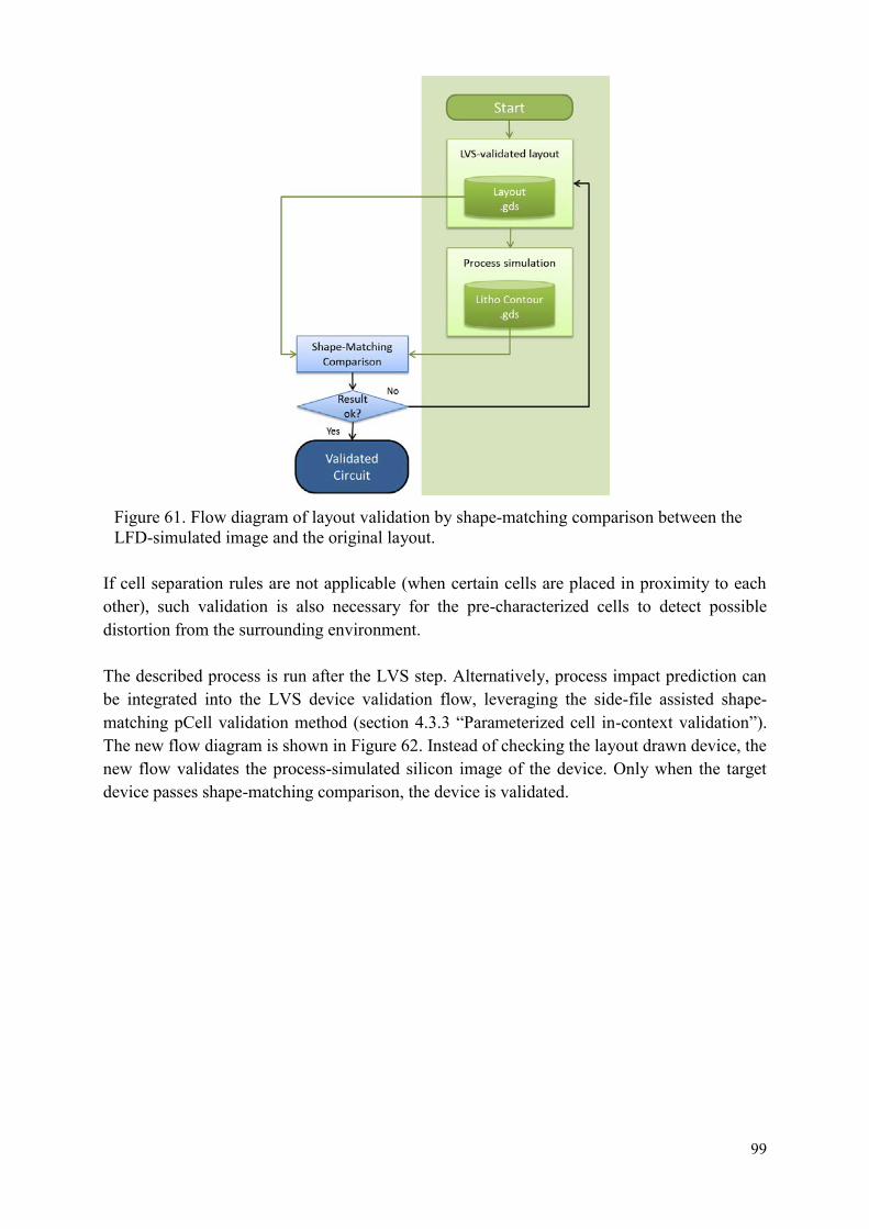
99
If cell separation rules are not applicable (when certain cells are placed in proximity to each other), such validation is also necessary for the pre-characterized cells to detect possible distortion from the surrounding environment. The described process is run after the LVS step. Alternatively, process impact prediction can be integrated into the LVS device validation flow, leveraging the side-file assisted shape-matching pCell validation method (section 4.3.3 “Parameterized cell in-context validation”).
The new flow diagram is shown in Figure 62. Instead of checking the layout drawn device, the new flow validates the process-simulated silicon image of the device. Only when the target device passes shape-matching comparison, the device is validated.
Figure 61. Flow diagram of layout validation by shape-matching comparison between the LFD-simulated image and the original layout.
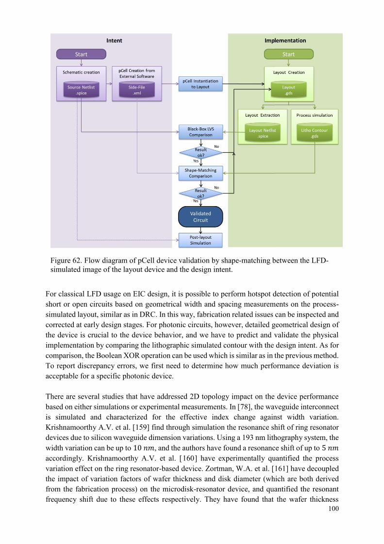
100
For classical LFD usage on EIC design, it is possible to perform hotspot detection of potential short or open circuits based on geometrical width and spacing measurements on the process-simulated layout, similar as in DRC. In this way, fabrication related issues can be inspected and corrected at early design stages. For photonic circuits, however, detailed geometrical design of the device is crucial to the device behavior, and we have to predict and validate the physical implementation by comparing the lithographic simulated contour with the design intent. As for comparison, the Boolean XOR operation can be used which is similar as in the previous method. To report discrepancy errors, we first need to determine how much performance deviation is acceptable for a specific photonic device. There are several studies that have addressed 2D topology impact on the device performance based on either simulations or experimental measurements. In [78], the waveguide interconnect is simulated and characterized for the effective index change against width variation. Krishnamoorthy A.V. et al. [159] find through simulation the resonance shift of ring resonator devices due to silicon waveguide dimension variations. Using a 193 nm lithography system, the width variation can be up to 10 𝑛𝑚, and the authors have found a resonance shift of up to 5 𝑛𝑚 accordingly. Krishnamoorthy A.V. et al. [160] have experimentally quantified the process variation effect on the ring resonator-based device. Zortman, W.A. et al. [161] have decoupled the impact of variation factors of wafer thickness and disk diameter (which are both derived from the fabrication process) on the microdisk-resonator device, and quantified the resonant frequency shift due to these effects respectively. They have found that the wafer thickness
Figure 62. Flow diagram of pCell device validation by shape-matching between the LFD-simulated image of the layout device and the design intent.
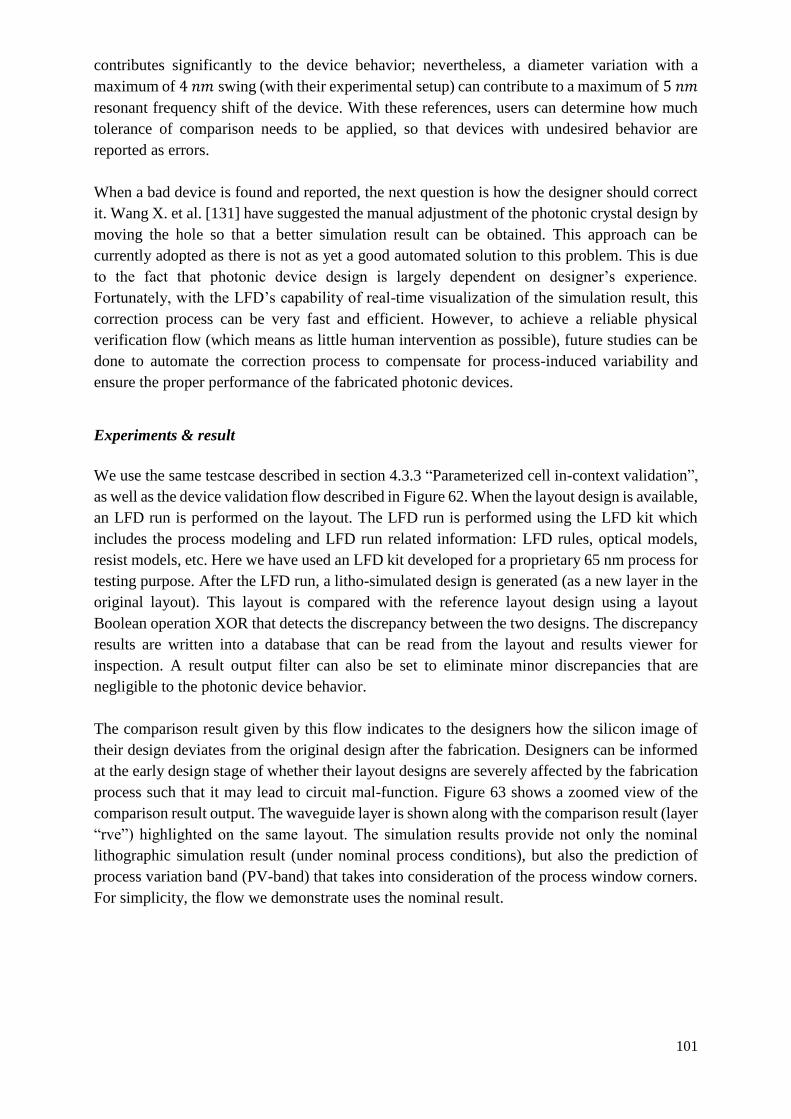
101
contributes significantly to the device behavior; nevertheless, a diameter variation with a
maximum of 4 𝑛𝑚 swing (with their experimental setup) can contribute to a maximum of 5 𝑛𝑚
resonant frequency shift of the device. With these references, users can determine how much
tolerance of comparison needs to be applied, so that devices with undesired behavior are
reported as errors.
When a bad device is found and reported, the next question is how the designer should correct
it. Wang X. et al. [131] have suggested the manual adjustment of the photonic crystal design by
moving the hole so that a better simulation result can be obtained. This approach can be
currently adopted as there is not as yet a good automated solution to this problem. This is due
to the fact that photonic device design is largely dependent on designer’s experience.
Fortunately, with the LFD’s capability of real-time visualization of the simulation result, this
correction process can be very fast and efficient. However, to achieve a reliable physical
verification flow (which means as little human intervention as possible), future studies can be
done to automate the correction process to compensate for process-induced variability and
ensure the proper performance of the fabricated photonic devices.
Experiments & result
We use the same testcase described in section 4.3.3 “Parameterized cell in-context validation”,
as well as the device validation flow described in Figure 62. When the layout design is available,
an LFD run is performed on the layout. The LFD run is performed using the LFD kit which
includes the process modeling and LFD run related information: LFD rules, optical models,
resist models, etc. Here we have used an LFD kit developed for a proprietary 65 nm process for
testing purpose. After the LFD run, a litho-simulated design is generated (as a new layer in the
original layout). This layout is compared with the reference layout design using a layout
Boolean operation XOR that detects the discrepancy between the two designs. The discrepancy
results are written into a database that can be read from the layout and results viewer for
inspection. A result output filter can also be set to eliminate minor discrepancies that are
negligible to the photonic device behavior.
The comparison result given by this flow indicates to the designers how the silicon image of
their design deviates from the original design after the fabrication. Designers can be informed
at the early design stage of whether their layout designs are severely affected by the fabrication
process such that it may lead to circuit mal-function. Figure 63 shows a zoomed view of the
comparison result output. The waveguide layer is shown along with the comparison result (layer
“rve”) highlighted on the same layout. The simulation results provide not only the nominal
lithographic simulation result (under nominal process conditions), but also the prediction of
process variation band (PV-band) that takes into consideration of the process window corners.
For simplicity, the flow we demonstrate uses the nominal result.
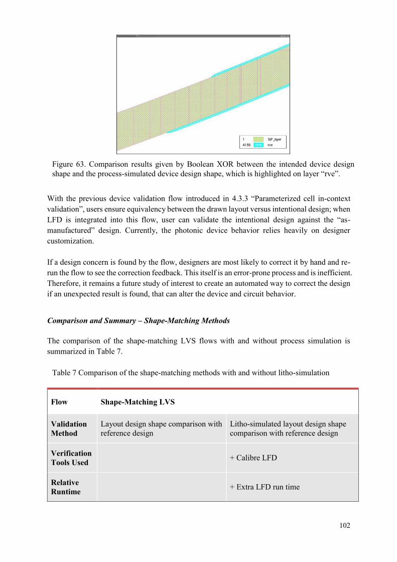
102
With the previous device validation flow introduced in 4.3.3 “Parameterized cell in-context validation”, users ensure equivalency between the drawn layout versus intentional design; when LFD is integrated into this flow, user can validate the intentional design against the “as-manufactured” design. Currently, the photonic device behavior relies heavily on designer
customization. If a design concern is found by the flow, designers are most likely to correct it by hand and re-run the flow to see the correction feedback. This itself is an error-prone process and is inefficient. Therefore, it remains a future study of interest to create an automated way to correct the design if an unexpected result is found, that can alter the device and circuit behavior.
Comparison and Summary – Shape-Matching Methods The comparison of the shape-matching LVS flows with and without process simulation is summarized in Table 7.
Flow Shape-Matching LVS
Validation Method
Layout design shape comparison with reference design
Litho-simulated layout design shape comparison with reference design
Verification Tools Used + Calibre LFD
Relative Runtime + Extra LFD run time
Figure 63. Comparison results given by Boolean XOR between the intended device design shape and the process-simulated device design shape, which is highlighted on layer “rve”.
Table 7 Comparison of the shape-matching methods with and without litho-simulation

103
Advantages Sufficient on relatively large and
separated designs
Better accuracy – Considering process
effect on critical designs
Drawbacks Empirical correction process if error is
found
Shape-matching with process-simulated layout is only necessary when the design pitch is below
65 nm. For small photonic component features like photonic crystals, a verification flow with
a LFD predicted silicon image greatly helps designers to early identify design failure due to the
fabrication process. However, it remains designer’s own task to correct the layout in order to
obtain better result that matches the design intent.
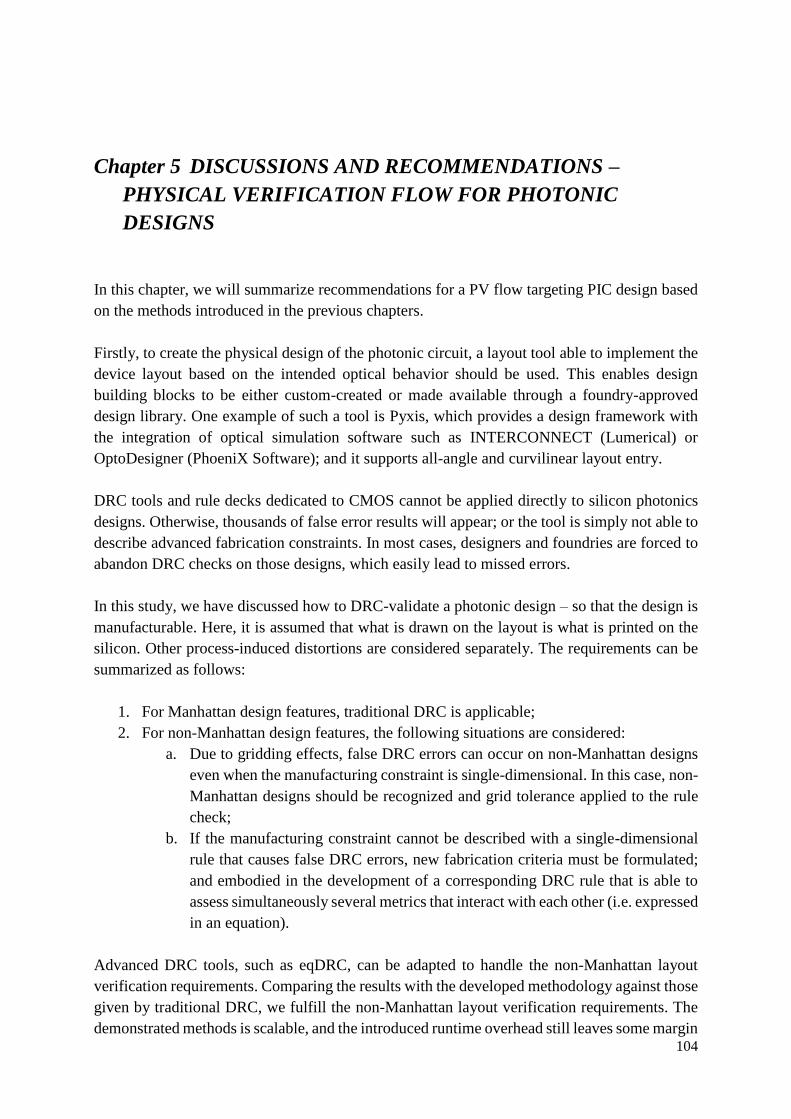
104
Chapter 5 DISCUSSIONS AND RECOMMENDATIONS –
PHYSICAL VERIFICATION FLOW FOR PHOTONIC
DESIGNS
In this chapter, we will summarize recommendations for a PV flow targeting PIC design based
on the methods introduced in the previous chapters.
Firstly, to create the physical design of the photonic circuit, a layout tool able to implement the
device layout based on the intended optical behavior should be used. This enables design
building blocks to be either custom-created or made available through a foundry-approved
design library. One example of such a tool is Pyxis, which provides a design framework with
the integration of optical simulation software such as INTERCONNECT (Lumerical) or
OptoDesigner (PhoeniX Software); and it supports all-angle and curvilinear layout entry.
DRC tools and rule decks dedicated to CMOS cannot be applied directly to silicon photonics
designs. Otherwise, thousands of false error results will appear; or the tool is simply not able to
describe advanced fabrication constraints. In most cases, designers and foundries are forced to
abandon DRC checks on those designs, which easily lead to missed errors.
In this study, we have discussed how to DRC-validate a photonic design – so that the design is
manufacturable. Here, it is assumed that what is drawn on the layout is what is printed on the
silicon. Other process-induced distortions are considered separately. The requirements can be
summarized as follows:
1. For Manhattan design features, traditional DRC is applicable;
2. For non-Manhattan design features, the following situations are considered:
a. Due to gridding effects, false DRC errors can occur on non-Manhattan designs
even when the manufacturing constraint is single-dimensional. In this case, non-
Manhattan designs should be recognized and grid tolerance applied to the rule
check;
b. If the manufacturing constraint cannot be described with a single-dimensional
rule that causes false DRC errors, new fabrication criteria must be formulated;
and embodied in the development of a corresponding DRC rule that is able to
assess simultaneously several metrics that interact with each other (i.e. expressed
in an equation).
Advanced DRC tools, such as eqDRC, can be adapted to handle the non-Manhattan layout
verification requirements. Comparing the results with the developed methodology against those
given by traditional DRC, we fulfill the non-Manhattan layout verification requirements. The
demonstrated methods is scalable, and the introduced runtime overhead still leaves some margin

105
as compared to electronic designs. The suggested practices to deal with non-Manhattan design
features are not common for traditional rules on Manhattan EIC structures. A traditional CMOS
process fab should be prepared to adopt these new methods. While the demonstrated
methodology and testcase have proven the feasibility to apply advanced DRC rules for photonic
layout, it is up to the foundry to define specific parameter constraints and equations, which
implies validation versus manufactured results.
DRC is specific to the fabrication process. Although silicon photonics uses existing CMOS
processes, the introduction of non-Manhattan features imposes the need to develop new
fabrication constraints. LVS rules are specific to the technology (whether it is an electronic
circuit or a photonic circuit, despite the fact that they may share the same fabrication process).
The circuit validation requirements are specific to the unique features of photonic designs. The
photonic circuit verification goals are summarized as followed:
1. The basic circuit topology, including device count, short- and open-circuits, can be
verified by using a “black-box” LVS method.
2. Manhattan device verification can be done with the traditional LVS tool and rule deck
implementation.
3. Photonic devices with complex non-Manhattan and curved features cannot be verified
by comparing a set of device properties. Therefore, shape-matching based comparison
is recommended:
a. For pre-characterized devices with fixed geometry (as opposed to pCells), a
shape-matching based method using golden device design libraries can be
applied to verify in-context device placement.
b. With the help of design software to preserve and pass full device geometry intent
(e.g. in curve equations), a shape-matching based method can be extended and
used to verify in-context pCell placement.
4. The curved design of waveguide interconnect should be verified according to different
cases as follows:
a. Critical waveguide interconnect that is intentionally designed (with intentional
design geometry and user-defined parameters) is placed and recognized as a
device. Its parameters are extracted and compared against the source.
b. Non-critical waveguide interconnect (without intentional design geometry and
user-specified parameters) is placed as an interconnection. Its parameters are
measured for validation against optical signal continuity checks.
5. LVS comparison between the intent and the predicted silicon image given by a process
simulation tool can provide a more accurate device validation outcome for the custom
device design. For the case of pre-characterized devices, such a validation can verify the
process influence when it is placed in-context, if necessary.
6. The parameters of these devices should be made available (in SPICE netlist) for post-
layout simulation.
The proposed LVS flow is shown as a diagram in Figure 58.
106
The existing EDA software tools support the basic circuit topology comparison for photonic designs once a proper LVS rule deck is in place. Devices with Manhattan features only (such as a photodetector) can also be validated with classical LVS tools. This is the minimum requirement for circuit validation if no advanced method exists to verify beyond the capabilities of classical EIC design tools. The rest of the circuit needs alternative validation methods. As summarized above, different verification methodologies need to be adopted on the various types of elements in the photonic circuit design according to their respective verification requirements. The waveguide interconnects are categorized into two types based on their function and corresponding design method. One is the critical waveguide interconnect type, which is laid out intentionally by designers, and parameters such as width and length (usually related to the phase engineering of light travelling in the waveguide) must be carefully controlled. Designers prefer to design the exact topology of the waveguide path of, for example, an MZI circuit. In this case, LVS property tracking, similar to that used for complete devices, should be applied. We extract salient waveguide parameters and compare with the source values captured from designer’s intent. As classical LVS tools hardly support measurements on curved shapes, such verification is done with the help of the extended curvilinear parameter extraction methods proposed in this study.
Figure 64. The proposed LVS flow diagram.
107
The other type of waveguide interconnect is non-critical – it functions as a pure signal
transmission channel and can be laid out using a semi-automated routing tool such as Pyxis.
Nevertheless, the geometrical design of such routing must be verified for parasitic effect
assessment and control. The ORC verification, which is an analogy to ERC in electronic designs,
is made possible by extended measurement methodologies and advanced circuit and layout
analysis tools such as Calibre PERC-LDL. This validation step ensures that the geometrical
design of the interconnect meets with optical signal continuity constraints.
For photonic devices like ring modulators, it is usually necessary to consider curved features.
Some techniques can be applied to measure and validate the device layout; however, photonic
device behavior can be determined by tiny geometrical modifications that are not easily
captured by a set of geometrical parameters. Therefore, shape-matching based methods are
recommended to validate complex photonic devices.
Verification methods like device signature matching and pattern matching can be used for
validating device cell designs with fixed parameters. Such methods require a pre-generated
golden device library. For parameterized cell designs, there is no golden design to be matched,
as the device is only instantiated after it is placed into the circuit. In this case, we recommend
methods that require the design software (like OptoDesigner) to preserve detailed device
geometrical information (e.g. in XML format) at the design intent phase, so that the placed
device layout can be validated later, based on shape-matching against the intent.
Furthermore, the shape-matching method can also leverage the process simulation result for
device validation. Instead of comparing design intent and the drawn layout, the device
validation is done between the design intent and the silicon image given by a process simulation
tool such as Calibre LFD, which gives a “manufactured vs. intent” comparison result. This
verification procedure is highly recommended, as process variation impact is critical on
photonic device behavior and has not yet been fully explored.
Lastly, layout netlists can be simulated with the layout-extracted device parameters, as well as
the preserved source parameters (as device text labels) from shape-matching validated devices.
The simulation is performed with help of photonic circuit simulation tools that can take SPICE
netlist inputs such as INTERCONNECT.
The above elements of the LVS flow is individually tested. Due to lack of PDK content, it is
yet to put all the pieces together and assess the performance of such a flow.
The recommended LVS flow described above can ensure that the physical implementation of
the photonic circuit design is conducted according to the intent. However, the match of layout
and design intent does not guarantee that the manufactured silicon behaves as the ideal design
intent. We have alerted users of process variation induced distortion by incorporating LFD into
LVS validation. However, the correction of the detected errors remains a manual process. Other
than this, the post-layout steps introduce manufacturing difficulties, as well as distortions from
the original layout. These are also critical issues that require future studies.

108
Currently, some photonic designers prefer a “layout-centric” design flow, meaning that they
start directly with the layout design without capturing a schematic beforehand. Usually, they
use separate software tools for performing simulation and implementing layout instead of using
an integrated design environment. The design data (building blocks, design schematic, layout,
etc.) is communicated through different design abstractions manually. For example, the process
of placing building blocks in the circuit design is manual, as is that of performing
(semi-)automatic routing; and LVS verification is not applicable in this case. When the design
is relatively small (typically some tens of photonic components in a circuit), researchers and
designers are satisfied with this design approach and are confident that they do not make any
mistakes during the design. However, as the silicon photonics technology comes out from
research labs to the production line, this design approach will not suffice for the design
efficiency and yield demanded by the industry. Demand is emerging for an integrated design
environment that automatically handles and verifies different types of design data throughout
the design flow. We have prepared the physical verification methodologies (DRC and LVS)
which are indispensable elements in this picture.
109
Chapter 6 CONCLUSIONS
With the technology being standardized over time, the success of silicon photonics products
will rely on system design and application differentiation, instead of physical level innovation.
A similar ecosystem is building up like that of the EIC industry. Foundries provide qualified
building block libraries to photonic designers; and designers customize their circuits and system
designs knowing only device specifications (and the allowed parameter variations in the case
of parameterized cells). This requires and drives the demand for an integrated design flow and
a reliable physical verification flow to achieve such a design methodology.
In this thesis, we propose generic methodologies to verify the physical design of silicon
photonics. We assess the verification requirements specific to photonic circuits, which cannot
be satisfied by directly applying classical PV tools and flows. The novel requirements derive
mainly from the curvilinear nature of the PIC layouts compared to EIC layouts, which are
usually rectilinear. The limitations of current DRC and LVS tools are analyzed.
We demonstrate the difficulties met when using traditional DRC tools and rules to validate the
photonic layout. Directly applying traditional DRC runs on photonic designs will result in an
unmanageably large number of false errors. Moreover, a single-dimensional DRC tool is not
capable of handling design constraints dedicated to non-Manhattan designs. We propose
advanced design rules, implemented with the equation-based DRC tool. The method enables
DRC on non-Manhattan-like layouts (and is not limited to photonic designs): eliminating false
errors and performing advanced (i.e. multi-dimensional) rule checks through the incorporation
of mathematical equations. The applied technique also prevents fatal missed errors which can
occur when excluding designs from DRC runs due to the incapability of traditional tools.
Traditional LVS tools can only achieve very limited accuracy in verifying photonic circuit
functionality against intent, i.e. the basic circuit topology. The specificity in photonic circuit
validation also lies in its curvilinear layout, as well as the fact that the behavior of photonic
components relies on their complex geometrical layouts. We propose methods that perform a
complete LVS run that validates layout components as waveguide interconnect, fixed-layout
photonic devices and parametric photonic devices. The developed methods are designed to
expect curvilinear features from those components; the complex geometrical topology that
needs to be exactly validated; and the potential unwanted interaction within the circuit context.
The ORC step is also proposed to perform DRC-like checks to account for optical circuit design
rules, e.g. addressing optical signal continuity concerns.
The lithographic and process variation effects are considered crucial to photonic device
behavior. Therefore, we incorporate such manufacturing effect prediction results into the LVS
check, enabling an “as-manufactured” versus intent comparison and validation.

110
The developed PV methods and flows are an inseparable part of the entire design flow. At the
PV stage, input from upstream design must be obtained and properly represent design intent,
e.g. for LVS comparison; its impact on downstream post-layout steps should also be taken into
consideration, e.g. for simulation that requires layout extraction results. Therefore, while this
work is focused on the development of a PV flow based on analyzing the design and verification
requirements, it affects the rest of the design flow steps as it imposes requirements on them.
The demonstrations are performed using industrial standard EDA tools, e.g. the Pyxis-based
unified design environment and Calibre PV tool suites. The verification requirement analysis
and the proposed methodologies are generic and can be equally useful to help adapt other EDA
tools.
By implementing the proposed PV flow which is based on the tool and PDK adaption and
customization, a more reliable PV analysis on silicon photonic design is achieved. Based on
this study, we propose several areas that can be interesting for future study:
1) Development of advanced fabrication rules based on the exploitation of manufacturing
capability: We have proposed in this study the necessity and feasibility of performing advanced
fabrication rule checking on non-Manhattan layout designs. However, it is up to the foundry to
characterize their process and adapt such non-Manhattan layout manufacturing. It is mandatory
to extensively verbalize and formulate fabrication constraints for non-Manhattan layout designs
based on actual process experiments or/and simulations. Although silicon photonics uses
existing CMOS manufacturing processes where fabrication constraints are already set up, the
introduction of advanced constraints is essential due to the existence of the non-Manhattan
layout of photonic designs. Designers, PDK engineers, process engineers need to collaborate
more closely to define the DRC rules and corresponding DRM.
2) Further assessment on process effect correction and mask discretization aspects: Process
simulation has been incorporated into the design and PV flow to accurately predict the actual
silicon image in the early design stages. It remains a manual and experimental process, however,
to carry out design corrections if an unaccepted result is found. Using current process correction
tools, it is proven that such correction can greatly improve the faithfulness of actual fabricated
silicon to design entry for Manhattan-like photonic components. In the case of non-Manhattan
layouts, such correction does not necessarily result in improvement. Further assessment on the
tools is required. Studies also suggest that distortion induced by mask discretization impacts
photonic component behavior; and the processing time for photonic designs is not ideal, as
compared to the processing time for Manhattan design masks. Future experiments can be carried
out to find the best compromise between discretization accuracy and processing time.
Furthermore, improved discretization algorithms that better adapt non-Manhattan/curved
designs can be developed.
3) Novel layout database and layout processing tools that genuinely support curvilinear data:
The limitations of the current tools in handling photonic layout design mostly come from its
non-Manhattan nature. For example, DRC issues include false errors induced by unexpected
dimensional measurement variation, and the lack of means to check non-rectilinear geometries;
LVS issues include the incapability of validating layout device and interconnect with curved
features. We have proposed methodologies and flows in this study to extend the tool capability

111
to resolve these issues, based on current industrial standard layout formats and layout processing
tools. The more progressive way to eliminate these issues is to introduce new layout formats
and tools that support curvilinear designs. The new format should be able to store complex
layout design information, probably represented as mathematical functions and/or parameters
for these functions. The tools should be able to deal with these design representations –
performing various measurements, extractions and manipulations. In this way, it can be
potentially less time-consuming as it avoids processing the large number of linear edges that
approximate the curvilinear design shapes. The approximation also forces the application of
tolerance when processing curved layout, e.g. in DRC dimension measurement, LVS device
feature extraction and comparison. Therefore, another advantage of directly processing original
design data is that it would greatly simplify the validation process. The introduction of such
new standards and methodologies might not get an easy entry into the existing mature design
flow and infrastructure for CMOS technology. It is therefore up to the silicon photonics market
to prove the worth of such efforts.
112
References
[1] Cisco. (2014). The Zettabyte Era – Trends and Analysis. [Online]. Available:
http://www.cisco.com/en/US/solutions/collateral/ns341/ns525/ns537/ns705/ns827/VNI_Hype
rconnectivity_WP.html
[2] Gordon, E. M. (1965). Cramming more components onto integrated circuits. Electronics Magazine.
[3] Friedrich, J., McCredie, B., James, N., Huott, B., Curran, B., Fluhr, E., … Lanzerotti, M.
(2007). Design of the Power6TM microprocessor. Digest of Technical Papers - IEEE International Solid-State Circuits Conference, 96–97.
[4] Dorsey, J., Searles, S., Ciraula, M., Johnson, S., Bujanos, N., Wu, D., … Kumar, R.
(2007). An Integrated Quad-Core Opteron Processor. 2007 IEEE International Solid-State Circuits Conference. Digest of Technical Papers, 102–103.
[5] Borkar, S., & Chien, A.-A. (2011). The future of microprocessors. Communications of the ACM, 54(5), 67.
[6] Shalf, J., Dosanjh, S., & Morrison, J. (2010). Exascale computing technology challenges.
High Performance Computing for Computational Science (VECPAR), 1–25.
[7] Miller, D.-A.-B. (1996). Limit to the Bit-Rate Capacity of Electrical Interconnects from
the Aspect Ratio of the System Architecture. Distributed Computing, 4252.
[8] Borkar, S. (2013). Role of interconnects in the future of computing. Journal of Lightwave Technology, 31(24), 3927–3933.
[9] Borkar, S. (1999). Design challenges of technology scaling. IEEE Micro, 19(4), 23–29.
[10] Magen, N., Kolodny, A., Weiser, U., & Shamir, N. (2004). Interconnect-power
dissipation in a microprocessor. Proceedings of the 2004 International Workshop on System Level Interconnect Prediction SLIP 04, (74), 7–13.
[11] Goodman, J.-W., Leonberger, F.-J., Kung, S.-Y., & Athale, R.-A. (1984). Optical
Interconnections for Vlsi Systems. Proceedings of the IEEE, 72(7), 850–866.
[12] Shacham, A., Bergman, K., & Carloni, L.-P. (2008). Photonic networks-on-chip for
future generations of chip multiprocessors. IEEE Transactions on Computers, 57(9), 1246–
1260.
[13] Iwai, H. (2009). Roadmap for 22nm and beyond (Invited Paper). Microelectronic Engineering, 86(7-9), 1520–1528.
[14] International Technology Roadmap for Semiconductors (ITRS). [Online]. Available:
www.itrs.net
[15] Arden, W., Brillouët, M., Cogez, P., Graef, M., Huizing, B., & Mahnkopf, R. More-than-
Moore, White Paper. [Online]. Available: http://www.itrs.net/ITRS%201999-
2014%20Mtgs,%20Presentations%20&%20Links/2010ITRS/IRC-ITRS-MtM-v2%203.pdf
[16] Cavin, R.-K., Lugli, P., & Zhirnov, V.-V. (2012). Science and engineering beyond
Moore’s law. Proceedings of the IEEE, 100(SPL CONTENT), 1720–1749.
[17] Carballo, J., Chan, W.-J., Gargini, P.-A., Kahng, A.-B., & Nath, S. (2014). ITRS 2.0:
Toward a re-framing of the Semiconductor Technology Roadmap. 2014 IEEE 32nd International Conference on Computer Design (ICCD), 139–146.
113
[18] O’Connor, I., & Gaffiot, F. (2005). Advanced Research in On-Chip Optical
Interconnects. Low-Power CMOS Circuits. 1–20.
[19] Haurylau, M., Chen, G., Chen, H., Zhang, J., Nelson, N.-A., Albonesi, D.-H., … Fauchet,
P.-M. (2006). On-chip optical interconnect roadmap: Challenges and critical directions. IEEE Journal on Selected Topics in Quantum Electronics, 12(6), 1699–1704.
[20] Shacham, A., Bergman, K., & Carloni, L.-P. (2008). Photonic networks-on-chip for
future generations of chip multiprocessors. IEEE Transactions on Computers, 57(9), 1246–
1260.
[21] O’Connor, I., Briere, M., Drouard, E., Kazmierczak, A., Tissafi-Drissi, F., Navarro,
D., … Gaffiot, F. (2005). Towards reconfigurable optical networks on chip. ReCoSoC, Invited Talk.
[22] Kachris, C., & Tomkos, I. (2012). A Survey on Optical Interconnects for Data Centers.
IEEE Communications Surveys & Tutorials, 14(4), 1021–1036.
[23] Iga, K. (2000). Surface-emitting laser - its birth and generation of new optoelectronics
field. IEEE Journal on Selected Topics in Quantum Electronics, 6(6), 1201–1215.
[24] Ghiasi, A. (2015). Large data centers interconnect bottlenecks. Optics Express, 23(3),
2085.
[25] “Luxtera” [Online]. Available: http://www.luxtera.com/
[26] Sahni, S., Narasimha, A., Mekis, A., Welch, B., Bradbury, C., Sohn, C., … Liang, Y.
(2012). Silicon Photonic Integrated Circuits. Conference on Lasers and Electro-Optics 2012,
CM3A.3.
[27] “Skorpios Technologies” [Online]. Available: http://www.skorpiosinc.com/
[28] “Mellanox Technologies” [Online]. Available: http://www.kotura.com/
[29] Denoyer, G., Cole, C., Santipo, A., Russo, R., Robinson, C., Li, L., … Vulliet, N. (2015).
Hybrid Silicon Photonic Circuits and Transceiver for 50 Gb/s NRZ Transmission Over
Single-Mode Fiber. Journal of Lightwave Technology, 33(6), 1247–1254.
[30] Doerr, C.-R., Chen, L., Vermeulen, D., Nielsen, T., Azemati, S., Stulz, S., … Park, S.-Y.
(2014). Single-Chip Silicon Photonics 100-Gb/s Coherent Transceiver. Optical Fiber Communication Conference: Postdeadline Papers, Th5C.1.
[31] Passaro, V.-M.-N., de Tullio, C., Troia, B., La Notte, M., Giannoccaro, G., & De Leonardis,
F. (2012). Recent advances in integrated photonic sensors. Sensors (Basel, Switzerland), 12(11),
15558–98.
[32] Passaro, V., Tullio, C., Troia, B., Notte, M., Giannoccaro, G., & Leonardis, F. (2012).
Recent Advances in Integrated Photonic Sensors. Sensors, 12(12), 15558–15598.
[33] Estevez, M.-C., Alvarez, M., & Lechuga, L.-M. (2012). Integrated optical devices for
lab-on-a-chip biosensing applications. Laser & Photonics Reviews, 6(4), 463–487.
[34] Soref, R. a., & Lorenzo, J.-P. (1985). Single-crystal silicon: a new material for 1.3 and
1.6 μm integrated-optical components. Electronics Letters, 21(21), 953.
[35] Liow, J., Yu, M. Bin, Lo, P., & Kwong, D.-L. (2010). Silicon photonics technologies for
monolithic electronic-photonic integrated circuit applications. In ICSICT-2010 - 2010 10th IEEE International Conference on Solid-State and Integrated Circuit Technology, Proceedings, 28, 29–32.
[36] Assefa, S., Shank, S., Green, W., Khater, M., Kiewra, E., Reinholm, C., … Vlasov, Y.
(2012). A 90nm CMOS integrated Nano-Photonics technology for 25Gbps WDM optical

114
communications applications. Technical Digest - International Electron Devices Meeting, IEDM, 10–12.
[37] Young, I.-A., Mohammed, E., Liao, J.-T.-S., Kern, A.-M., Palermo, S., Block, B.-A., …
Chang, P.-L.-D. (2010). Optical I/O Technology for Tera-Scale Computing. IEEE Journal of Solid-State Circuits, 45(1), 235–248.
[38] Menezo, S., Duprez, H., Descos, A., Bordel, D., Sanchez, L., Brianceau, P., … Ben Bakir,
B. (2014). Advances on III-V on Silicon DBR and DFB Lasers for WDM Optical Interconnects
and Associated Heterogeneous Integration 200mm-Wafer-Scale Technology. 2014 IEEE Compound Semiconductor Integrated Circuit Symposium (CSICS), 1–6.
[39] Papes M., Cheben P., Ye W.-N., Schmid J.-H., … Vašinek V. (2015). Fiber-chip edge
coupler with large mode size for silicon photonic wire waveguides. Proc. SPIE 9516, Integrated Optics: Physics and Simulations II, 95160K.
[40] Van Laere, F., Bogaerts, W., Taillaert, D., Dumon, P., Van Thourhout, D., & Baets, R.
(2007). Compact focusing grating couplers between optical fibers and silicon-on-insulator
photonic wire waveguides. OFC/NFOEC 2007 - Optical Fiber Communication and the National Fiber Optic Engineers Conference 2007, 1–3.
[41] Reed, G.-T., Mashanovich, G., Gardes, F.-Y., & Thomson, D.-J. (2010). Silicon optical
modulators. Nature Photonics, 4(8), 518–526.
[42] Michel, J., Liu, J., & Kimerling, L.-C. (2010). High-performance Ge-on-Si
photodetectors. Nature Photonics, 4(8), 527–534.
[43] Wang, J., & Lee, S. (2011). Ge-photodetectors for Si-based optoelectronic integration.
Sensors, 11(1), 696–718.
[44] Brouckaert, J., Roelkens, G., Van Thourhout, D., & Baets, R. (2007). Compact InAlAs-
InGaAs metal-semiconductor-metal photodetectors integrated on silicon-on-insulator
waveguides. IEEE Photonics Technology Letters, 19(19), 1484–1486.
[45] Fathpour, S. (2015). Emerging heterogeneous integrated photonic platforms on silicon.
Nanophotonics, 4(1), 143–164.
[46] Heck, M.-J.-R., Chen, H.-W., Fang, A.-W., Koch, B.-R., Liang, D., Park, H., … Bowers,
J.-E. (2011). Hybrid Silicon Photonics for Optical Interconnects. IEEE Journal of Selected Topics in Quantum Electronics, 17(2), 333–346.
[47] Heck, M., Davenport, M., & Bowers, J. (2013). Progress in hybrid-silicon photonic
integrated circuit technology. SPIE Newsroom, 17(2), 28–33.
[48] Lockwood, D.-J., & Pavesi, L. (2004). Silicon Photonics, Volume 1. Silicon Photonics, Volume 1. Springer Science & Business Media. Section 2.2, p59.
[49] “MACOM Announces Definitive Agreement to Acquire BinOptics Corporation.” Nov
2014. [Online]. Available: http://ir.macom.com/releasedetail.cfm?releaseid=883689
[50] “MACOM's Commitment to Silicon Photonics.” Nov 2014. [Online]. Available: http://www.macom.com/technologies/siph
[51] Huawei completes acquisition of Caliopa. Sep 2013. [Online]. Available: http://caliopa.com/news-and-events/article/huawei-completes-acquisition-of-caliopa
[52] Avago Technologies to Acquire CyOptics, a Leading Optical Chip and Component
Supplier to the Datacom and Telecom Markets. April 2013. [Online]. Available: http://investors.avagotech.com/phoenix.zhtml?c=203541&p=irol-newsArticle&ID=1805814
[53] Mellanox Technologies, Ltd. Completes Acquisition of Kotura, Inc. Aug 2013. [Online]. Available: http://www.mellanox.com/page/press_release_item?id=1096

115
[54] “Cisco Completes Acquisition of Lightwire”, Mar 2012. [Online]. Available: http://www.cisco.com/web/about/ac49/ac0/ac1/ac259/lightwire.html
[55] “Molex Purchases Luxtera‟s Silicon Photonics-based Active Optical Cable (AOC)
Business”, Jan 2011. [Online]. Available: http://www.luxtera.com/20110111226/molex-
purchases-luxtera%E2%80%99s-silicon-photonics-based-active-optical-cable-aoc-business-
partners-on-future-aoc-development.html
[56] “The PLAT4M (Photonic Libraries And Technology for Manufacturing) project.”
[Online]. Available: http://plat4m-fp7.eu/
[57] “pHotonics ELectronics functional Integration on CMOS.” [Online]. Available: http://www.helios-project.eu/
[58] “Integrated Photonics Institute for Manufacturing Innovation (IP-IMI).” [Online]. Available: http://manufacturing.gov/ip-imi.html
[59] “Ultraperformance Nanophotonic Intrachip Communication (UNIC).” [Online]. Available: https://www.fbo.gov/index?s=opportunity&mode=form&id=d7786e93a3d2df276eb7a25301cd180f&tab=core&_cview=1 [60] “Photonics and Electronics convergence Technology Research Association.” [Online]. Available: http://www.petra-jp.org/e/index-e.html
[61] “National Basic Research Program of China.” [Online]. Available: http://www.973.gov.cn/English/Index.aspx
[62] “National High-tech R&D Program (863 Program).” [Online]. Available: http://www.most.gov.cn/eng/programmes1/
[63] Hochberg, M., & Baehr-Jones, T. (2010). Towards fabless silicon photonics. Nature Photonics, 4(8), 492–494.
[64] Hochberg, M., Harris, N.-C., Ding, R., Zhang, Y., Novack, A., Xuan, Z., & Baehr-Jones,
T. (2013). Silicon Photonics: The next fabless semiconductor industry Michael. IEEE Solid-State Circuits Magazine, 48–58.
[65] Lim, A. E.-J., Song, J., Fang, Q., Li, C., Tu, X., Duan, N., … Liow, T.-Y. (2014). Review
of Silicon Photonics Foundry Efforts. IEEE Journal of Selected Topics in Quantum Electronics, 20(4), 8300112.
[66] “The University of British Columbia, Si-EPIC Program.” [Online]. Available: http://siepic.ubc.ca/
[67] “ePIXfab, the Silicon photonics platform.” [Online]. Available: http://www.epixfab.eu/
[68] Dumon, P., Bogaerts, W., Baets, R., Fedeli, J.-M., & Fulbert, L. (2009). Towards foundry
approach for silicon photonics: silicon photonics platform ePIXfab. Electronics Letters,
45(12), 581.
[69] “Luxtera Announces Production Status of World’s First Commercial Silicon CMOS
Photonics Fabrication Process” [Online]. Available: http://www.luxtera.com/20090603183/luxtera-announces-production-status-of-worlds-1st-
commercial-silicon-cmos-photonics-fabrication-process.html
[70] Sahni, S., Narasimha, A., Mekis, A., Welch, B., Bradbury, C., Sohn, C., … Liang, Y.
(2012). Silicon Photonic Integrated Circuits. Conference on Lasers and Electro-Optics 2012,
CM3A.3.
[71] Cunningham, J.-E., Shubin, I., Thacker, H.-D., Lee, J.-H., Li, G., Zheng, X., …
Krishnamoorthy, A. V. (2012). Scaling hybrid-integration of silicon photonics in Freescale

116
130nm to TSMC 40nm-CMOS VLSI drivers for low power communications. Proceedings - Electronic Components and Technology Conference, 1518–1525.
[72] “Luxtera and STMicroelectronics to Enable High-Volume Silicon Photonics Solutions.”
[Online]. Available: http://www.st.com/web/en/press/cn/t3279
[73] Boeuf, F., Cremer, S., Temporiti, E., Fere, M., Shaw, M., Vulliet, N., … Verga, L.
(2015), Recent progress in Silicon Photonics R&D and manufacturing on 300mm wafer
platform. Optical Fiber Communications Conference and Exhibition (OFC), 2015 , 1-3.
[74] Eu, A., Lim, J., Liow, T., Song, J., Li, C., Fang, Q., … Lo, G. (2014). Path to Silicon
Photonics Commercialization : 25 Gb / s Platform Development in a CMOS Manufacturing
Foundry Line, (Ild), 2–4.
[75] Orcutt, J.-S., Khilo, A., Popović, M.-A., Holzwarth, C.-W., Moss, B., Li, H., …
Stojanović, V. (2008). Demonstration of an electronic photonic integrated circuit in a
commercial scaled bulk CMOS process. 2008 Conference on Quantum Electronics and Laser Science Conference on Lasers and Electro-Optics, CLEO/QELS, (c), 3–4.
[76] Baets, R. (2011). Building a sustainable future for silicon photonics. 8th IEEE International Conference on Group IV Photonics, 3–4.
[77] Fulbert, L., & Fedeli, J.-M. (2011). Photonics–Electronics integration on CMOS. 2011 Proceedings of the European Solid-State Device Research Conference (ESSDERC), 13–18.
[78]Passaro V.-N.-M., & De Leonardis, F. (2008). Recent Advances in Modelling and
Simulation of Silicon Photonic Devices. In Modelling and Simulation. I-Tech Education and
Publishing.
[79] Scarmozzino, R., Gopinath, A., Pregla, R., & Helfert, S. (2000). Numerical techniques
for modeling guided-wave photonic devices. IEEE Journal of Selected Topics in Quantum Electronics, 6(1), 150–162.
[80] Stoffer, R. (2004). Comparison of Coupled Mode Theory and FDTD Simulations of
Coupling between Bent and Straight Optical Waveguides. AIP Conference Proceedings, 709,
366–377.
[81] Lowery, A.-J. (1997). Computer-aided photonics design. IEEE Spectrum, 34(4), 26–31.
[82] Arellano, C., Mingaleev, S., Koltchanov, I., Richter, A., Pomplun, J., Burger, S., &
Schmidt, F. (2013). Efficient design of photonic integrated circuits (PICs) by combining
device- and circuit- level simulation tools. In J. E. Broquin & G. Nunzi Conti (Eds.), Proc. SPIE, Integrated Optics: Devices, Materials, and Technologies XVII, 8627, 862711.
[83] Leijtens, X.-J.-M., Le Lourec, P., & Smit, M.-K. (1996). S-matrix oriented CAD-tool for
simulating complex integrated optical circuits. IEEE Journal on Selected Topics in Quantum Electronics, 2(2), 257–262.
[84] Pêcheux, F., Lallement, C., & Vachoux, A. (2005). VHDL-AMS and Verilog-AMS as
alternative hardware description languages for efficient modeling of multidiscipline systems.
IEEE Transactions on Computer-Aided Design of Integrated Circuits and Systems, 24(2), 204–
224.
[85] Martin, P., Gays, F., Grellier, E., Myko, A., & Menezo, S. (2014). Modeling of silicon
photonics devices with Verilog-A. 2014 29th International Conference on Microelectronics Proceedings - MIEL 2014, 209–212.
[86] Zhu, K., Saxena, V., & Kuang, W. (2014). Compact Verilog-A modeling of silicon
traveling-wave modulator for hybrid CMOS photonic circuit design. 2014 IEEE 57th International Midwest Symposium on Circuits and Systems (MWSCAS), 615–618.

117
[87] Rhim, J., Ban, Y., Yu, B.-M., Lee, J.-M., & Choi, W.-Y. (2015). Verilog-A behavioral
model for resonance-modulated silicon micro-ring modulator. Optics Express, 23(7), 8762.
[88] Melati, D., Morichetti, F., Soares, F.-M., & Melloni, A. (2012). Building block based
design of photonic integrated circuits for generic photonic foundries. 2012 14th International Conference on Transparent Optical Networks (ICTON), 1–4.
[89] O’Connor, I., & Nicolescu, G. (2013). Integrated Optical Inerconnect Architectures for Embedded Systems. (I. O’Connor & G. Nicolescu, Eds.). New York, NY: Springer New York.
[90] Glick, M., Rumley, S., Dongaonkar, G., Li, Q., Bergman, K., & Dutt, R. (2013). Silicon
photonic interconnection networks for data centers. 2013 IEEE Photonics Society Summer Topical Meeting Series, 2, 244–245.
[91] Ding, D., & Pan, D.-Z. (2009). OIL: A Nano-photonics Optical Interconnect Library for a
New Photonic Networks-on-Chip Architecture. Proceedings of the 11th International Workshop on System Level Interconnect Prediction - SLIP ’09, 11–18.
[92] Minz, J.-R., Thyagara, S., & Lim, S.-K. (2007). Optical routing for 3-D system-on-
package. IEEE Transactions on Components and Packaging Technologies, 30(4), 805–812.
[93] Boos, A., Ramini, L., Schlichtmann, U., & Bertozzi, D. (2013). PROTON: An automatic
place-and-route tool for optical networks-on-chip. IEEE/ACM International Conference on Computer-Aided Design, Digest of Technical Papers, ICCAD, 138–145.
[94] Hendry, G., Chan, J., Carloni, L. P., & Bergman, K. (2011). VANDAL: A tool for the
design specification of nanophotonic networks. 2011 Design, Automation & Test in Europe,
1–6.
[95] O’Connor, I., Tissafi-Drissi, F., Gaffiot, F., Dambre, J., De Wilde, M., Van Campenhout,
J., … Stroobandt, D. (2007). Systematic simulation-based predictive synthesis of integrated
optical interconnect. IEEE Transactions on Very Large Scale Integration (VLSI) Systems,
15(8), 927–939.
[96] Hochberg, M., & Harris, N. (2013). Silicon Photonics: The Next Fabless Semiconductor
Industry. Solid-State Circuits …, 48–58.
[97] Bogaerts, W., Dumon, P., Lambert, E., Fiers, M., Pathak, S., & Ribeiro, A. (2012).
IPKISS: A parametric design and simulation framework for silicon photonics. The 9th International Conference on Group IV Photonics (GFP), 2, 30–32.
[98] “PDAFlow Foundation.” [Online]. Available: http://www.pdaflow.org/
[99] “OptoDesigner 5: The Ultimate Photonic Chip Design Environment.” [Online]. Available: http://www.phoenixbv.com/optodesigner
[100] “Photonic Integrated Circuit Design with Lumerical INTERCONNECT and PhoeniX.”
[Online]. Available: https://www.lumerical.com/phoenix/
[101] “INTERCONNECT: Time and frequency domain simulation of bidirectional,
multimode and multichannel circuit topologies.” [Online]. Available:
https://www.lumerical.com/support/whitepaper/interconnect_circuit_solver/
[102] “VPIphotonics and Phoenix Software ease design of Photonic Integrated Circuits by
bridging circuit-level optimization and mask layout generation.” [Online]. Available: http://www.vpiphotonics.com/Services/Downloads/DownloadArea/Files/VPIphotonics-
PhoeniX_PressRelease-PhotWest2015.pdf
[103] “IPKISS and L-Edit integrate Photonic IC Design.” [Online]. Available: https://community.si2.org/posts/995787-ipkiss-and-l-edit-integrate-photonic-ic-design
118
[104] Bogaerts, W., Fiers, M., & Dumon, P. (2014). Design Challenges in Silicon Photonics.
IEEE Journal of Selected Topics in Quantum Electronics, 20(4), 1–8.
[105] “Mentor Graphics and Lumerical Unify Optical Design and Simulation Flow.”
[Online]. Available: http://www.mentor.com/company/news/mentor-lumerical-optical-design
[106] Wade, M., Stojanovic, V., Ram, R., Alloatti, L., Popovic, M. (2015), Photonics design
tool for advanced CMOS nodes. IET Optoelectronics, 9 (4), 163-167.
[107] Welch, B. (2014). Silicon photonics: The road to commercialization. In Open Server Summit, 1–24.
[108] Batten, C., Joshi, A., Orcutt, J., Khilo, A., Moss, B., Holzwarth, C., … Asanovic, K.
(2008). Building Manycore Processor-to-DRAM Networks with Monolithic Silicon
Photonics. 2008 16th IEEE Symposium on High Performance Interconnects, 21–30.
[109] Fedeli, J., Schrank, F., Augendre, E., Bernabe, S., Kraft, J., Grosse, P., & Enot, T.
(2014). Photonic - Electronic Integration With Bonding. IEEE Journal of Selected Topics in Quantum Electronics, 20(4), 350–358.
[110] Sun, C., Wade, M.-T., Lee, Y., Orcutt, J. S., Alloatti, L., Georgas, M.-S., … Stojanović,
V.-M. (2015). Single-chip microprocessor that communicates directly using light. Nature,
528(7583), 534–538.
[111] Fedeli, J. M., Augendre, E., Hartmann, J. M., Vivien, L., Grosse, P., Mazzocchi, V., …
Schrankd, F. (2010). Photonics and electronics integration in the HELIOS project. IEEE International Conference on Group IV Photonics GFP, 356–358.
[112] “IBM’s Silicon Photonics Technology Ready to Speed up Cloud and Big Data
Applications.” [Online]. Available: https://www-
03.ibm.com/press/us/en/pressrelease/46839.wss
[113] Kaminow, I.-P., & Koch, T.-L. (1997). Optical Fiber Telecommunications III.
Academic Press, 334.
[114] Marcatili, E. a. J. (1969). Bends in Optical Dielectric Guides. Bell System Technical Journal, 48(7), 2103–2132.
[115] Ferguson, J., & Fedor, P., (2013). Proposed best practices in silicon photonics layout vs.
schematic physical verification. Group IV Photonics (GFP), 2013 IEEE 10th International Conference on, 120-121.
[116] Vivien, L., & Pavesi, L. (2013). Handbook of silicon photonics. Boca Raton, FL: Taylor
& Francis.
[117] Reed, G.-T. (2004). Silicon photonics: an introduction. Chichester ; Hoboken, NJ: John
Wiley.
[118] Van Laere, F., Bogaerts, W., Taillaert, D., Dumon, P., Van Thourhout, D., & Baets, R.
(2007). Compact Focusing Grating Couplers Between Optical Fibers and Silicon-on-Insulator
Photonic Wire Waveguides. OFC/NFOEC 2007 Conference on Optical Fiber Communication and the National Fiber Optic Engineers Conference, 1–3.
[119] Marcatili, E., & Miller, S. (1969). Improved relations describing directional control in
electromagnetic wave guidance. Bell System Technical Journal. [120] Lee, H., Chen, T., Li, J., Painter, O., & Vahala, K.-J. (2012). Ultra-low-loss optical
delay line on a silicon chip. Nature Communications, 3(20), 867.
[121] Mustieles, F.-J., Ballesteros, E., & Baquero, P. (1993). Theoretical S-bend profile for
optimization of optical waveguide radiation losses. IEEE Photonics Technology Letters, 5(5).

119
[122] Vlasov, Y.-A., & McNab, S.-J. (2004). Losses in single-mode silicon-on-insulator strip
waveguides and bends. Optics Express, 12(8), 1622.
[123] Heiblum, M., & Harris, J. (1975). Analysis of curved optical waveguides by conformal
transformation. IEEE Journal of Quantum Electronics, 2, 75–83.
[124] Gunn, C. (2007). Fully integrated VLSI CMOS and photonics “CMOS photonics.”
Digest of Technical Papers - Symposium on VLSI Technology, 3, 6–9.
[125] Chrostowski, L., Wang, X., Flueckiger, J., Wu, Y., Wang, Y., & Talebi Fard, S. (2014).
Impact of Fabrication Non-Uniformity on Chip-Scale Silicon Photonic Integrated Circuits.
Optical Fiber Communication Conference, Th2A.37.
[126] Zortman, W. a, Trotter, D.-C., & Watts, M.-R. (2010). Silicon photonics manufacturing. Optics Express, 18(23), 23598–23607.
[127] Selvaraja, S.-K.; Bogaerts, W.; Dumon, P.; Van Thourhout, D.; Baets, R. (2010).
Subnanometer Linewidth Uniformity in Silicon Nanophotonic Waveguide Devices Using
CMOS Fabrication Technology. Selected Topics in Quantum Electronics, IEEE Journal of, 16(1), 316-324.
[128] Teo, H.-G., Yu, M.-B., Doan, M.-T., Singh, J., Sun, H.-Q., & Liu, A.-Q. (2004). 248nm
lithography of 2D photonic crystal waveguide with optical proximity correction. Digest of the LEOS Summer Topical Meetings Biophotonics/Optical Interconnects and VLSI Photonics/WBM Microcavities, 2004. 2966, 87–88
[129] Bogaerts, W., Dumon, P., Wiaux, V., Wouters, J., Beckx, S., & Baets, R. (2003).
Tolerance Control for Photonic Crystal Structures Fabricated With Deep UV Lithography.
ECOC, 46–47.
[130] “Calibre® LFD™ (Litho Friendly Design).” [Online]. Available: http://www.mentor.com/products/ic_nanometer_design/design-for-manufacturing/calibre-lfd/
[131] Wang, X.; Shi; W., Hochberg, M.; Adam, K.; Schelew, E.; Young, J.-F.; …
Chrostowski, L. (2012). Lithography simulation for the fabrication of silicon photonic devices
with deep-ultraviolet lithography. Group IV Photonics (GFP), 2012 IEEE 9th International Conference on, 29-31.
[132] Bogaerts, W., Bradt, P., Vanholme, L., Bienstman, P., & Baets, R. (2008). Closed-loop
modeling of silicon nanophotonics from design to fabrication and back again. Optical and Quantum Electronics, 40, 801–811.
[133] Lee, C.-D., Chen, W.-C.-W., Wang, Q., Chen, Y.-J., Beard, W.-T., Stone, D., …
Stewart, I.-R. (2001). The role of photomask resolution on the performance of arrayed-
waveguide grating devices. Journal of Lightwave Technology, 19(11), 1726–1733.
[134] Pathak, S., Vanslembrouck, M., Dumon, P., Van Thourhout, D., Verheyen, P., Lepage,
G., … Bogaerts, W. (2014). Effect of mask discretization on performance of silicon arrayed
waveguide gratings. IEEE Photonics Technology Letters, 26(7), 718–721.
[135] Cinque, R., Komagata, T., Kiuchi, T., Browning, C., Schiavone, P., Petroni, P., …
Quaglio, T. (2013). Shot count reduction for non-Manhattan geometries: concurrent
optimization of data fracture and mask writer design, SPIE 8880, Photomask Technology 2013, 88801F.
[136] The CGAL Project. (2015). CGAL User and Reference Manual. CGAL Editorial Board,
4.7 edition.
[137] Buck, P., Gladhill, R., & Straub, J. (2007). Mask manufacturing rules checking (MRC)
as a DFM strategy. SPIE 6521, Design for Manufacturability through Design-Process Integration, 65211V.
120
[138] Abercrombie, D., & Ferguson, J. (2009). Equation-Based DRC: A Novel Approach to
Resolving Complex Nanometer Design Issues. DesignCon 2009, Santa Clara, California, 14.
[139] Pikus, F.-G., & Abercrombie, D.-A. (2008). Model-based design verification. US Patent
App. 11/986,564.
[140] Juneidi, Z., Torki, K., & Hamza, R. (2000). Design rules for non- Manhattan shapes.
Micromachining and Microfabrication Process Technology VI, 4174, 200–206.
[141] Chrostowski, L., & Hochberg, M. (2015) Silicon Photonics Design: From Devices to
Systems. Cambridge University Press.
[142] “Generic Silicon Photonics PDK & Design Methdology.” [Online]. Available: http://siepic.ubc.ca/GSiP
[143] “Mentor Graphics Pyxis – Custom IC Design.” [Online]. Available: http://www.mentor.com/products/ic_nanometer_design/custom-ic-design/
[144] Hu, Z., & Lu, Y. Y. (2007). Computing optimal waveguide bends with constant width.
Journal of Lightwave Technology, 25(10), 3161–3167.
[145] Bogaerts, W., & Selvaraja, S. K. (2011). Compact single-mode silicon hybrid rib/strip
waveguide with adiabatic bends. IEEE Photonics Journal, 3(3), 422–432.
[146] Worring, M., & Smeulders, A. (1993) Digital curvature estimation. CVGIP: Image Understanding.
[147] Hermann, S., & Klette, R. (2007). A Comparative Study on 2D Curvature Estimators.
2007 International Conference on Computing: Theory and Applications (ICCTA’07), 584–
589.
[148] Coeurjolly, D., Miguet, S., & Tougne, L. (2001). Discrete curvature based on osculating
circle estimation. Visual Form 2001, 303–312.
[149] Ahlberg, J.-H., Nilson, E.-N., & Walsh, J.-L., The theory of splines and their
applications. New York, Academic Press, 1967.
[150] Hazewinkel, M. (1998). Encyclopaedia of mathematics: an updated and annotated
translation of the Soviet ”Mathematical encyclopaedia”. Dordrecht ; Boston : Norwell, MA,
U.S.A: Reidel ; Sold and distributed in the U.S.A. and Canada by Kluwer Academic
Publishers.
[151] Pikus, F., Lu, Z., & Brooks, P. (2010). “Programmable electrical rule checking,” US
Patent App. 12/474,240.
[152] Kollu, K., Jackson, T., Kharas, F., & Adke, A. (2012). Unifying design data during
verification: Implementing Logic-Driven Layout analysis and debug. 2012 IEEE International Conference on IC Design & Technology, 1–5.
[153] Smit, M.-K. (1988). New focusing and dispersive planar component based on an optical
phased array. Electronics Letters, 24(7), 385.
[154] Dainesi, P., Küng, a., Chabloz, M., Lagos, a., Flückiger, P., Ionescu, A., … Robert, P.
(2000). CMOS compatible fully integrated Mach-Zehnder interferometer in SOI technology.
IEEE Photonics Technology Letters, 12(6), 660–662.

121
[155] Pathak, S., Vanslembrouck, M., Dumon, P., Van Thourhout, D., Verheyen, P., Lepage,
P., … Bogaerts, W. (2014). Effect of mask discretization on performance of silicon arrayed
waveguide gratings. IEEE Photonics Technology Letters, 26(7), 718–721.
[156] Koranne, S. (2015). Design and Analysis of Silicon Photonics Wave Guides Using
Symbolic Methods. IEEE Transactions on Computer-Aided Design of Integrated Circuits and Systems, 34(3), 341–353.
[157] “Extensible Markup Language (XML) 1.0.” [Online]. Available: http://www.w3.org/TR/REC-xml/
[158] “TclXML.” [Online]. Available: http://wiki.tcl.tk/1950 [159] Krishnamoorthy, A. V., Schwetman, H., Koka, P., Shubin, I., & Cunningham, J. E.
(2009). Computer Systems Based on Silicon Photonic Interconnects. Proceedings of the IEEE,
97(7), 1337–1361.
[160] Krishnamoorthy, A. V., Zheng, X., Li, G., Yao, J., Pinguet, T., Mekis, A., …
Cunningham, J. E. (2011). Exploiting CMOS Manufacturing to Reduce Tuning Requirements
for Resonant Optical Devices. IEEE Photonics Journal, 3(3), 567–579.
[161] Zortman, W. A., Watts, M. R., & Trotter, D. C. (2009). Determination Of Wafer And
Process Induced Resonant Frequency Variation In Silicon Microdisk-Resonators. Integrated Photonics and Nanophotonics Research and Applications 2009, 4–6.

![Tutorials for Layout, DRC, and LVS - Georgia Institute of ... for Layout, DRC, and LVS ... Choose option: No tech library needed ... Calibre Edit Verify Connectivity Options [abcd]](https://img.pdfslide.net/doc/110x75/5b4778b67f8b9a40638bee05/tutorials-for-layout-drc-and-lvs-georgia-institute-of-for-layout-drc-and.jpg)