Embed Size (px)
Citation preview
Bsouthnorth
OUT
0 mT
0 V
VCC
VL (MIN)
VL (MAX)
VCC / 2OUT
DRV5055
VCC
Controller
VCC
GND
ADC
Copyright © 2017, Texas Instruments Incorporated
Product
Folder
Order
Now
Technical
Documents
Tools &
Software
Support &Community
An IMPORTANT NOTICE at the end of this data sheet addresses availability, warranty, changes, use in safety-critical applications,intellectual property matters and other important disclaimers. PRODUCTION DATA.
DRV5055SBAS640 –JANUARY 2018
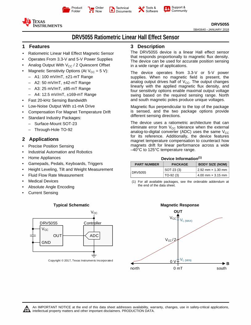
DRV5055 Ratiometric Linear Hall Effect Sensor
1
1 Features1• Ratiometric Linear Hall Effect Magnetic Sensor• Operates From 3.3-V and 5-V Power Supplies• Analog Output With VCC / 2 Quiescent Offset• Magnetic Sensitivity Options (At VCC = 5 V):
– A1: 100 mV/mT, ±21-mT Range– A2: 50 mV/mT, ±42-mT Range– A3: 25 mV/mT, ±85-mT Range– A4: 12.5 mV/mT, ±169-mT Range
• Fast 20-kHz Sensing Bandwidth• Low-Noise Output With ±1-mA Drive• Compensation For Magnet Temperature Drift• Standard Industry Packages:
– Surface-Mount SOT-23– Through-Hole TO-92
2 Applications• Precise Position Sensing• Industrial Automation and Robotics• Home Appliances• Gamepads, Pedals, Keyboards, Triggers• Height Leveling, Tilt and Weight Measurement• Fluid Flow Rate Measurement• Medical Devices• Absolute Angle Encoding• Current Sensing
3 DescriptionThe DRV5055 device is a linear Hall effect sensorthat responds proportionally to magnetic flux density.The device can be used for accurate position sensingin a wide range of applications.
The device operates from 3.3-V or 5-V powersupplies. When no magnetic field is present, theanalog output drives half of VCC. The output changeslinearly with the applied magnetic flux density, andfour sensitivity options enable maximal output voltageswing based on the required sensing range. Northand south magnetic poles produce unique voltages.
Magnetic flux perpendicular to the top of the packageis sensed, and the two package options providedifferent sensing directions.
The device uses a ratiometric architecture that caneliminate error from VCC tolerance when the externalanalog-to-digital converter (ADC) uses the same VCCfor its reference. Additionally, the device featuresmagnet temperature compensation to counteract howmagnets drift for linear performance across a wide–40°C to 125°C temperature range.
Device Information(1)
PART NUMBER PACKAGE BODY SIZE (NOM)
DRV5055SOT-23 (3) 2.92 mm × 1.30 mmTO-92 (3) 4.00 mm × 3.15 mm
(1) For all available packages, see the orderable addendum atthe end of the data sheet.
Typical Schematic Magnetic Response
2
DRV5055SBAS640 –JANUARY 2018 www.ti.com
Product Folder Links: DRV5055
Submit Documentation Feedback Copyright © 2018, Texas Instruments Incorporated
Table of Contents1 Features .................................................................. 12 Applications ........................................................... 13 Description ............................................................. 14 Revision History..................................................... 25 Pin Configuration and Functions ......................... 36 Specifications......................................................... 3
6.1 Absolute Maximum Ratings ...................................... 36.2 ESD Ratings.............................................................. 46.3 Recommended Operating Conditions....................... 46.4 Thermal Information .................................................. 46.5 Electrical Characteristics........................................... 46.6 Magnetic Characteristics........................................... 56.7 Typical Characteristics .............................................. 6
7 Detailed Description .............................................. 87.1 Overview ................................................................... 87.2 Functional Block Diagram ......................................... 87.3 Feature Description................................................... 8
7.4 Device Functional Modes........................................ 128 Application and Implementation ........................ 13
8.1 Application Information............................................ 138.2 Typical Application .................................................. 148.3 Do's and Don'ts ...................................................... 16
9 Power Supply Recommendations ...................... 1710 Layout................................................................... 17
10.1 Layout Guidelines ................................................. 1710.2 Layout Examples................................................... 17
11 Device and Documentation Support ................. 1811.1 Documentation Support ........................................ 1811.2 Receiving Notification of Documentation Updates 1811.3 Community Resources.......................................... 1811.4 Trademarks ........................................................... 1811.5 Electrostatic Discharge Caution............................ 1811.6 Glossary ................................................................ 18
12 Mechanical, Packaging, and OrderableInformation ........................................................... 18
4 Revision HistoryNOTE: Page numbers for previous revisions may differ from page numbers in the current version.
DATE REVISION NOTESJanuary 2018 * Initial release.
GND OUTVCC
1 2 3
GND
VCC
OUT
1
2
3
3
DRV5055www.ti.com SBAS640 –JANUARY 2018
Product Folder Links: DRV5055
Submit Documentation FeedbackCopyright © 2018, Texas Instruments Incorporated
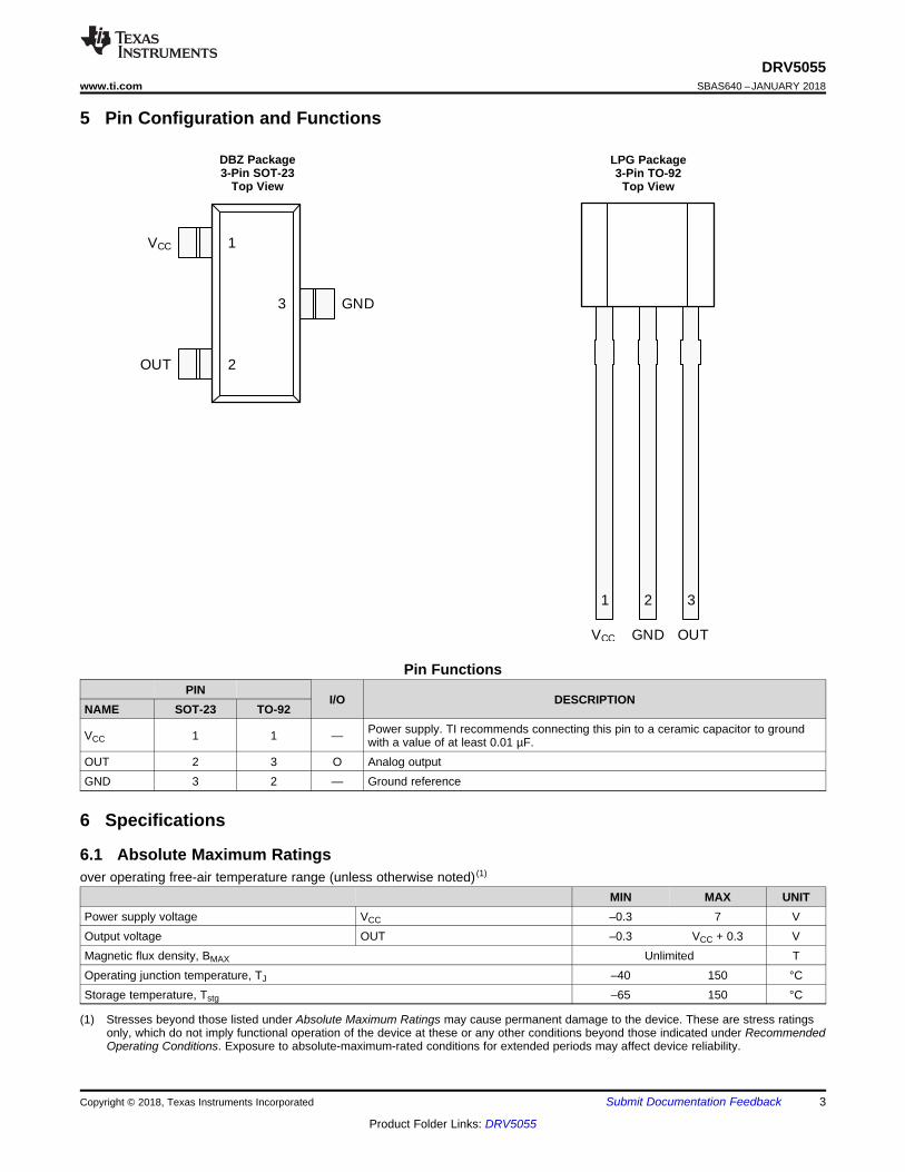
5 Pin Configuration and Functions
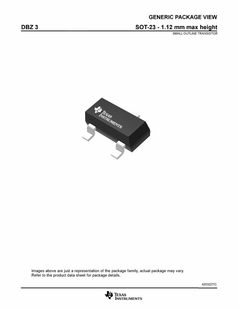
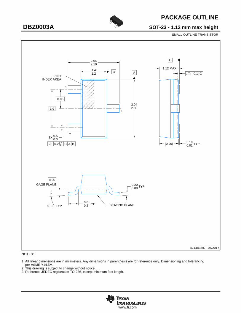
DBZ Package3-Pin SOT-23
Top View
LPG Package3-Pin TO-92
Top View
Pin FunctionsPIN
I/O DESCRIPTIONNAME SOT-23 TO-92
VCC 1 1 — Power supply. TI recommends connecting this pin to a ceramic capacitor to groundwith a value of at least 0.01 µF.
OUT 2 3 O Analog outputGND 3 2 — Ground reference
(1) Stresses beyond those listed under Absolute Maximum Ratings may cause permanent damage to the device. These are stress ratingsonly, which do not imply functional operation of the device at these or any other conditions beyond those indicated under RecommendedOperating Conditions. Exposure to absolute-maximum-rated conditions for extended periods may affect device reliability.
6 Specifications
6.1 Absolute Maximum Ratingsover operating free-air temperature range (unless otherwise noted) (1)
MIN MAX UNITPower supply voltage VCC –0.3 7 VOutput voltage OUT –0.3 VCC + 0.3 VMagnetic flux density, BMAX Unlimited TOperating junction temperature, TJ –40 150 °CStorage temperature, Tstg –65 150 °C
4
DRV5055SBAS640 –JANUARY 2018 www.ti.com
Product Folder Links: DRV5055
Submit Documentation Feedback Copyright © 2018, Texas Instruments Incorporated
(1) JEDEC document JEP155 states that 500-V HBM allows safe manufacturing with a standard ESD control process.(2) JEDEC document JEP157 states that 250-V CDM allows safe manufacturing with a standard ESD control process.
6.2 ESD RatingsVALUE UNIT
V(ESD) Electrostatic discharge
Human-body model (HBM), per ANSI/ESDA/JEDEC JS-001 (1) ±2500
VCharged-device model (CDM), per JEDEC specificationJESD22-C101 (2) ±750
(1) There are two isolated operating VCC ranges. For more information see the Operating VCC Ranges section.(2) Power dissipation and thermal limits must be observed.
6.3 Recommended Operating Conditionsover operating free-air temperature range (unless otherwise noted)
MIN MAX UNIT
VCC Power supply voltage (1) 3 3.63V
4.5 5.5IO Output continuous current –1 1 mATA Operating ambient temperature (2) –40 125 °C
(1) For more information about traditional and new thermal metrics, see the Semiconductor and IC Package Thermal Metrics applicationreport.
6.4 Thermal Information
THERMAL METRIC (1)DRV5055
UNITSOT-23 (DBZ) TO-92 (LPG)3 PINS 3 PINS
RθJA Junction-to-ambient thermal resistance 170 121 °C/WRθJC(top) Junction-to-case (top) thermal resistance 66 67 °C/WRθJB Junction-to-board thermal resistance 49 97 °C/WYJT Junction-to-top characterization parameter 1.7 7.6 °C/WYJB Junction-to-board characterization parameter 48 97 °C/W
(1) B is the applied magnetic flux density.(2) VN describes voltage noise on the device output. If the full device bandwidth is not needed, noise can be reduced with an RC filter.
6.5 Electrical Characteristicsfor VCC = 3 V to 3.63 V and 4.5 V to 5.5 V, over operating free-air temperature range (unless otherwise noted)
PARAMETER TEST CONDITIONS (1) MIN TYP MAX UNITICC Operating supply current 6 10 mAtON Power-on time (see Figure 11) B = 0 mT, no load on OUT 175 330 µsfBW Sensing bandwidth 20 kHztd Propagation delay time From change in B to change in OUT 10 µs
BND Input-referred RMS noise densityVCC = 5 V 130
nT/√HzVCC = 3.3 V 215
BN Input-referred noise BND × 6.6 × √20 kHzVCC = 5 V 0.12
mTPPVCC = 3.3 V 0.2
VN Output-referred noise (2) BN × S
DRV5055A1 12
mVPPDRV5055A2 6DRV5055A3 3DRV5055A4 1.5
5
DRV5055www.ti.com SBAS640 –JANUARY 2018
Product Folder Links: DRV5055
Submit Documentation FeedbackCopyright © 2018, Texas Instruments Incorporated
(1) B is the applied magnetic flux density.(2) See the Ratiometric Architecture section.(3) BL describes the minimum linear sensing range at 25°C taking into account the maximum VQ and Sensitivity tolerances.(4) See the Sensitivity Linearity section.(5) STC describes the rate the device increases Sensitivity with temperature. For more information, see the Sensitivity Temperature
Compensation For Magnets section.
6.6 Magnetic Characteristicsfor VCC = 3 V to 3.63 V and 4.5 V to 5.5 V, over operating free-air temperature range (unless otherwise noted)
PARAMETER TEST CONDITIONS (1) MIN TYP MAX UNIT
VQ Quiescent voltage B = 0 mT, TA = 25°CVCC = 5 V 2.43 2.5 2.57
VVCC = 3.3 V 1.59 1.65 1.71
VQΔT Quiescent voltage temperature drift B = 0 mT,TA = -40°C to 125°C versus 25°C ±1% × VCC V
VQRE Quiescent voltage ratiometry error (2) ±0.2%
VQΔL Quiescent voltage lifetime drift High-temperature operating stress for1000 hours <0.5%
S Sensitivity
VCC = 5 V,TA = 25°C
DRV5055A1 95 100 105
mV/mT
DRV5055A2 47.5 50 52.5DRV5055A3 23.8 25 26.2DRV5055A4 11.9 12.5 13.2
VCC = 3.3 V,TA = 25°C
DRV5055A1 57 60 63DRV5055A2 28.5 30 31.5DRV5055A3 14.3 15 15.8DRV5055A4 7.1 7.5 7.9
BL Linear magnetic sensing range (3) (4)
VCC = 5 V,TA = 25°C
DRV5055A1 ±21
mT
DRV5055A2 ±42DRV5055A3 ±85DRV5055A4 ±169
VCC = 3.3 V,TA = 25°C
DRV5055A1 ±22DRV5055A2 ±44DRV5055A3 ±88DRV5055A4 ±176
VL Linear range of output voltage (4) 0.2 VCC – 0.2 V
STCSensitivity temperature compensationfor magnets (5) 0.12 %/°C
SLE Sensitivity linearity error (4) VOUT is within VL ±1%SSE Sensitivity symmetry error (4) VOUT is within VL ±1%
SRE Sensitivity ratiometry error (2) TA = 25°C,with respect to VCC = 3.3 V or 5 V –2.5% 2.5%
SΔL Sensitivity lifetime drift High-temperature operating stress for1000 hours <0.5% %
Supply Voltage (V)
Sen
sitiv
ity (
mV
/mT
)
3 3.1 3.2 3.3 3.4 3.5 3.65
10
15
20
25
30
35
40
45
50
55
60
65
70
D006
DRV5055A1DRV5055A2DRV5055A3DRV5055A4
Supply Voltage (V)
Sen
sitiv
ity (
mV
/mT
)
4.5 4.6 4.7 4.8 4.9 5 5.1 5.2 5.3 5.4 5.50
20
40
60
80
100
120
D007
DRV055A1DRV055A2DRV055A3DRV055A4
Temperature (qC)
Sen
sitiv
ity (
mV
/mT
)
-40 -20 0 20 40 60 80 100 120 1400
20
40
60
80
D004
DRV5055A1DRV5055A2DRV5055A3DRV5055A4
Temperature (qC)
Sen
sitiv
ity (
mV
/mT
)
-40 -20 0 20 40 60 80 100 120 1400
20
40
60
80
100
120
D005
DRV5055A1DRV5055A2DRV5055A3DRV5055A4
Temperature (qC)
Qui
esce
nt V
olta
ge (
V)
-40 -20 0 20 40 60 80 100 120 1401.6
1.8
2
2.2
2.4
2.6
D002
VCC = 3.3 VVCC = 5 V
Supply Voltage (V)
Qui
esce
nt V
olta
ge (
V)
3 3.25 3.5 3.75 4 4.25 4.5 4.75 5 5.25 5.51.4
1.6
1.8
2
2.2
2.4
2.6
2.8
D003
6
DRV5055SBAS640 –JANUARY 2018 www.ti.com
Product Folder Links: DRV5055
Submit Documentation Feedback Copyright © 2018, Texas Instruments Incorporated
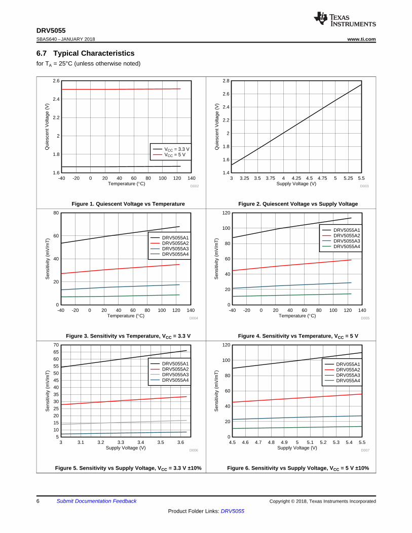
6.7 Typical Characteristicsfor TA = 25°C (unless otherwise noted)
Figure 1. Quiescent Voltage vs Temperature Figure 2. Quiescent Voltage vs Supply Voltage
Figure 3. Sensitivity vs Temperature, VCC = 3.3 V Figure 4. Sensitivity vs Temperature, VCC = 5 V
Figure 5. Sensitivity vs Supply Voltage, VCC = 3.3 V ±10% Figure 6. Sensitivity vs Supply Voltage, VCC = 5 V ±10%
Temperature (qC)
Ope
ratin
g S
uppl
y C
urre
nt (
mA
)
-40 -20 0 20 40 60 80 100 120 1405.2
5.4
5.6
5.8
6
6.2
6.4
6.6
D001
VCC = 3.3 VVCC = 5 V
7
DRV5055www.ti.com SBAS640 –JANUARY 2018
Product Folder Links: DRV5055
Submit Documentation FeedbackCopyright © 2018, Texas Instruments Incorporated
Typical Characteristics (continued)for TA = 25°C (unless otherwise noted)
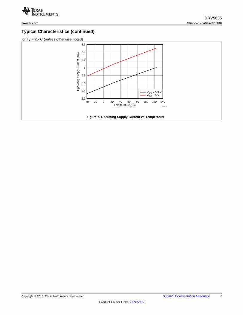
Figure 7. Operating Supply Current vs Temperature
PCB
SOT-23
B
B
TO-92
0.01 �F(minimum)
VCC
Output Driver
OUT
GND
VCC
Optional filter
Element Bias
Offset Cancellation
Temperature Compensation
Precision Amplifier
Bandgap Reference
Trim Registers
Copyright © 2017, Texas Instruments Incorporated
8
DRV5055SBAS640 –JANUARY 2018 www.ti.com
Product Folder Links: DRV5055
Submit Documentation Feedback Copyright © 2018, Texas Instruments Incorporated
7 Detailed Description
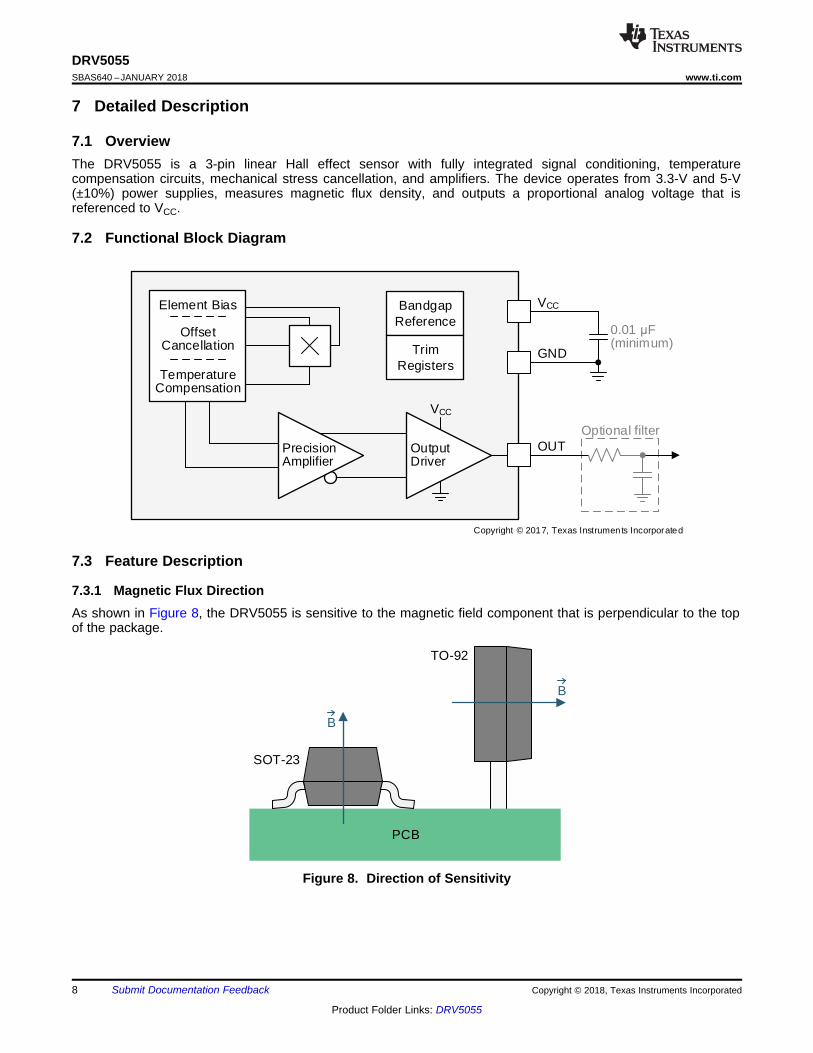
7.1 OverviewThe DRV5055 is a 3-pin linear Hall effect sensor with fully integrated signal conditioning, temperaturecompensation circuits, mechanical stress cancellation, and amplifiers. The device operates from 3.3-V and 5-V(±10%) power supplies, measures magnetic flux density, and outputs a proportional analog voltage that isreferenced to VCC.
7.2 Functional Block Diagram
7.3 Feature Description
7.3.1 Magnetic Flux DirectionAs shown in Figure 8, the DRV5055 is sensitive to the magnetic field component that is perpendicular to the topof the package.
Figure 8. Direction of Sensitivity
VOUT = VQ + B × Sensitivity(25° C) × (1 + STC × (TA ± 25° C))( )
PCBPCB
N
S
NS
9
DRV5055www.ti.com SBAS640 –JANUARY 2018
Product Folder Links: DRV5055
Submit Documentation FeedbackCopyright © 2018, Texas Instruments Incorporated
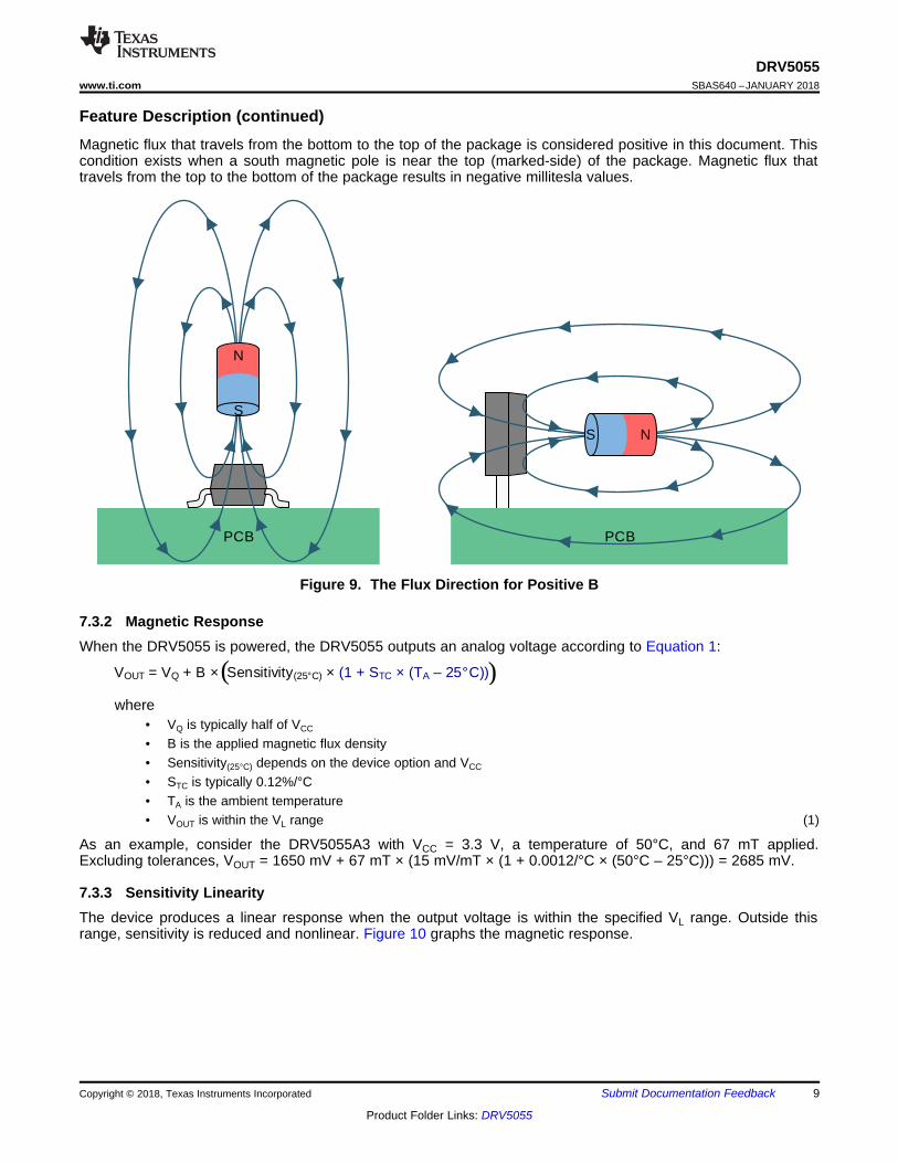
Feature Description (continued)Magnetic flux that travels from the bottom to the top of the package is considered positive in this document. Thiscondition exists when a south magnetic pole is near the top (marked-side) of the package. Magnetic flux thattravels from the top to the bottom of the package results in negative millitesla values.
Figure 9. The Flux Direction for Positive B
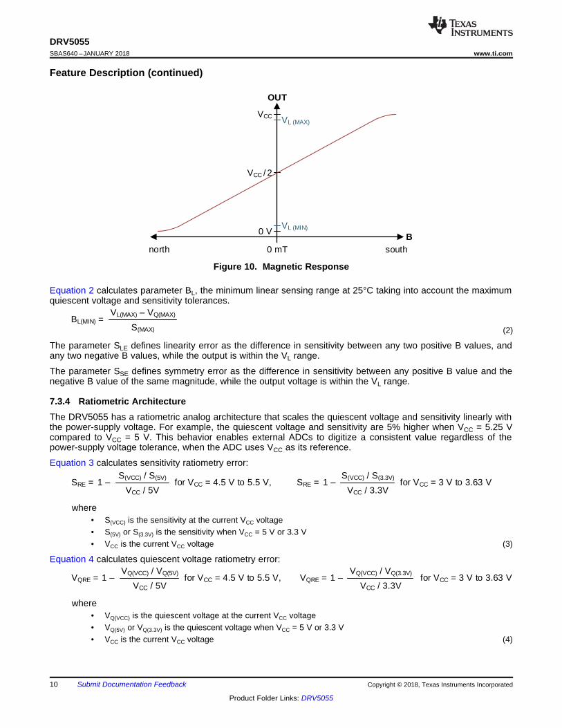
7.3.2 Magnetic ResponseWhen the DRV5055 is powered, the DRV5055 outputs an analog voltage according to Equation 1:
where• VQ is typically half of VCC
• B is the applied magnetic flux density• Sensitivity(25°C) depends on the device option and VCC
• STC is typically 0.12%/°C• TA is the ambient temperature• VOUT is within the VL range (1)
As an example, consider the DRV5055A3 with VCC = 3.3 V, a temperature of 50°C, and 67 mT applied.Excluding tolerances, VOUT = 1650 mV + 67 mT × (15 mV/mT × (1 + 0.0012/°C × (50°C – 25°C))) = 2685 mV.
7.3.3 Sensitivity LinearityThe device produces a linear response when the output voltage is within the specified VL range. Outside thisrange, sensitivity is reduced and nonlinear. Figure 10 graphs the magnetic response.
VQ(VCC) / VQ(3.3V)1 ±
VCC / 3.3VVQRE = for VCC = 3 V to 3.63 V
VQ(VCC) / VQ(5V)1 ±
VCC / 5VVQRE = for VCC = 4.5 V to 5.5 V,
S(VCC) / S(3.3V)1 ±
VCC / 3.3VSRE = for VCC = 3 V to 3.63 V
S(VCC) / S(5V)1 ±
VCC / 5VSRE = for VCC = 4.5 V to 5.5 V,
VL(MAX) ± VQ(MAX)
S(MAX)
BL(MIN) =
Bsouthnorth
OUT
0 mT
0 V
VCC
VL (MIN)
VL (MAX)
VCC / 2
10
DRV5055SBAS640 –JANUARY 2018 www.ti.com
Product Folder Links: DRV5055
Submit Documentation Feedback Copyright © 2018, Texas Instruments Incorporated
Feature Description (continued)
Figure 10. Magnetic Response
Equation 2 calculates parameter BL, the minimum linear sensing range at 25°C taking into account the maximumquiescent voltage and sensitivity tolerances.
(2)
The parameter SLE defines linearity error as the difference in sensitivity between any two positive B values, andany two negative B values, while the output is within the VL range.
The parameter SSE defines symmetry error as the difference in sensitivity between any positive B value and thenegative B value of the same magnitude, while the output voltage is within the VL range.
7.3.4 Ratiometric ArchitectureThe DRV5055 has a ratiometric analog architecture that scales the quiescent voltage and sensitivity linearly withthe power-supply voltage. For example, the quiescent voltage and sensitivity are 5% higher when VCC = 5.25 Vcompared to VCC = 5 V. This behavior enables external ADCs to digitize a consistent value regardless of thepower-supply voltage tolerance, when the ADC uses VCC as its reference.
Equation 3 calculates sensitivity ratiometry error:
where• S(VCC) is the sensitivity at the current VCC voltage• S(5V) or S(3.3V) is the sensitivity when VCC = 5 V or 3.3 V• VCC is the current VCC voltage (3)
Equation 4 calculates quiescent voltage ratiometry error:
where• VQ(VCC) is the quiescent voltage at the current VCC voltage• VQ(5V) or VQ(3.3V) is the quiescent voltage when VCC = 5 V or 3.3 V• VCC is the current VCC voltage (4)
VCC
time
3 VtON
Output
time
95% × VQ
Invalid
11
DRV5055www.ti.com SBAS640 –JANUARY 2018
Product Folder Links: DRV5055
Submit Documentation FeedbackCopyright © 2018, Texas Instruments Incorporated
Feature Description (continued)7.3.5 Operating VCC RangesThe DRV5055 has two recommended operating VCC ranges: 3 V to 3.63 V and 4.5 V to 5.5 V. When VCC is inthe middle region between 3.63 V to 4.5 V, the device continues to function, but sensitivity is less knownbecause there is a crossover threshold near 4 V that adjusts device characteristics.
7.3.6 Sensitivity Temperature Compensation For MagnetsMagnets generally produce weaker fields as temperature increases. The DRV5055 compensates by increasingsensitivity with temperature, as defined by the parameter STC. The sensitivity at TA = 125°C is typically 12%higher than at TA = 25°C.
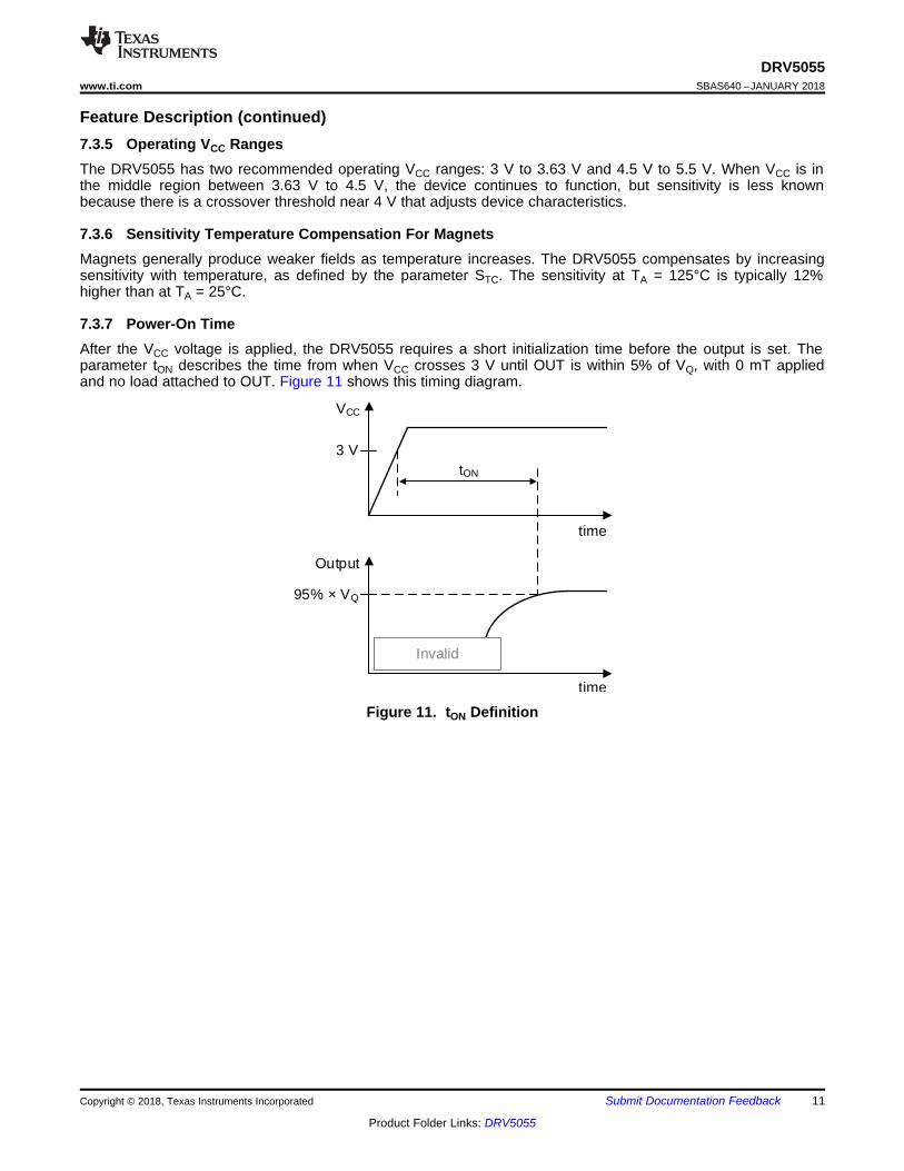
7.3.7 Power-On TimeAfter the VCC voltage is applied, the DRV5055 requires a short initialization time before the output is set. Theparameter tON describes the time from when VCC crosses 3 V until OUT is within 5% of VQ, with 0 mT appliedand no load attached to OUT. Figure 11 shows this timing diagram.
Figure 11. tON Definition
SOT-23Top View
TO-92Top View
650 µm±80 µm
SOT-23 Side View
centered±50 µm
1.61 mm
1.54 mm
2 mm 2 mm
±50 µm 1030 µm±115 µm
TO-92 Side View
12
DRV5055SBAS640 –JANUARY 2018 www.ti.com
Product Folder Links: DRV5055
Submit Documentation Feedback Copyright © 2018, Texas Instruments Incorporated
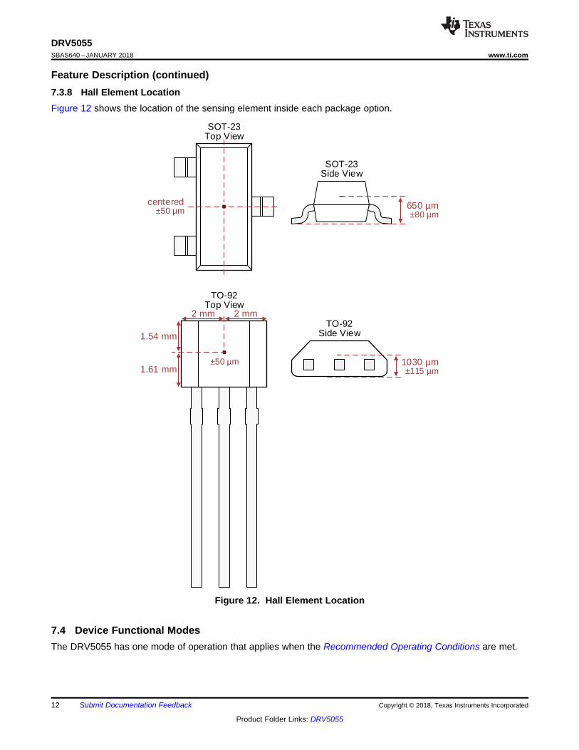
Feature Description (continued)7.3.8 Hall Element LocationFigure 12 shows the location of the sensing element inside each package option.
Figure 12. Hall Element Location
7.4 Device Functional ModesThe DRV5055 has one mode of operation that applies when the Recommended Operating Conditions are met.
OUT
DRV5055
VCC
GND
VCC
Cable
PCB
VOUT
Copyright © 2017, Texas Instruments Incorporated
13
DRV5055www.ti.com SBAS640 –JANUARY 2018
Product Folder Links: DRV5055
Submit Documentation FeedbackCopyright © 2018, Texas Instruments Incorporated
8 Application and Implementation
NOTEInformation in the following applications sections is not part of the TI componentspecification, and TI does not warrant its accuracy or completeness. TI’s customers areresponsible for determining suitability of components for their purposes. Customers shouldvalidate and test their design implementation to confirm system functionality.
8.1 Application Information
8.1.1 Selecting the Sensitivity OptionSelect the highest DRV5055 sensitivity option that can measure the required range of magnetic flux density, sothat the output voltage swing is maximized.
Larger-sized magnets and farther sensing distances can generally enable better positional accuracy than verysmall magnets at close distances, because magnetic flux density increases exponentially with the proximity to amagnet. TI created an online tool to help with simple magnet calculations at http://www.ti.com/product/drv5013.
8.1.2 Temperature Compensation for MagnetsThe DRV5055 temperature compensation is designed to directly compensate the average drift of neodymium(NdFeB) magnets and partially compensate ferrite magnets. The residual induction (Br) of a magnet typicallyreduces by 0.12%/°C for NdFeB, and 0.20%/°C for ferrite. When the operating temperature of a system isreduced, temperature drift errors are also reduced.
8.1.3 Adding a Low-Pass FilterAs shown in the Functional Block Diagram, an RC low-pass filter can be added to the device output for thepurpose of minimizing voltage noise when the full 20-kHz bandwidth is not needed. This filter can improve thesignal-to-noise ratio (SNR) and overall accuracy. Do not connect a capacitor directly to the device output withouta resistor in between because doing so can make the output unstable.
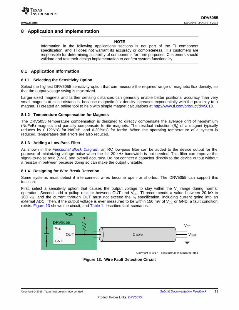
8.1.4 Designing for Wire Break DetectionSome systems must detect if interconnect wires become open or shorted. The DRV5055 can support thisfunction.
First, select a sensitivity option that causes the output voltage to stay within the VL range during normaloperation. Second, add a pullup resistor between OUT and VCC. TI recommends a value between 20 kΩ to100 kΩ, and the current through OUT must not exceed the IO specification, including current going into anexternal ADC. Then, if the output voltage is ever measured to be within 150 mV of VCC or GND, a fault conditionexists. Figure 13 shows the circuit, and Table 1 describes fault scenarios.
Figure 13. Wire Fault Detection Circuit
S N
14
DRV5055SBAS640 –JANUARY 2018 www.ti.com
Product Folder Links: DRV5055
Submit Documentation Feedback Copyright © 2018, Texas Instruments Incorporated
Table 1. Fault Scenarios and the Resulting VOUT
FAULT SCENARIO VOUT
VCC disconnects Close to GNDGND disconnects Close to VCC
VCC shorts to OUT Close to VCC
GND shorts to OUT Close to GND
8.2 Typical Application
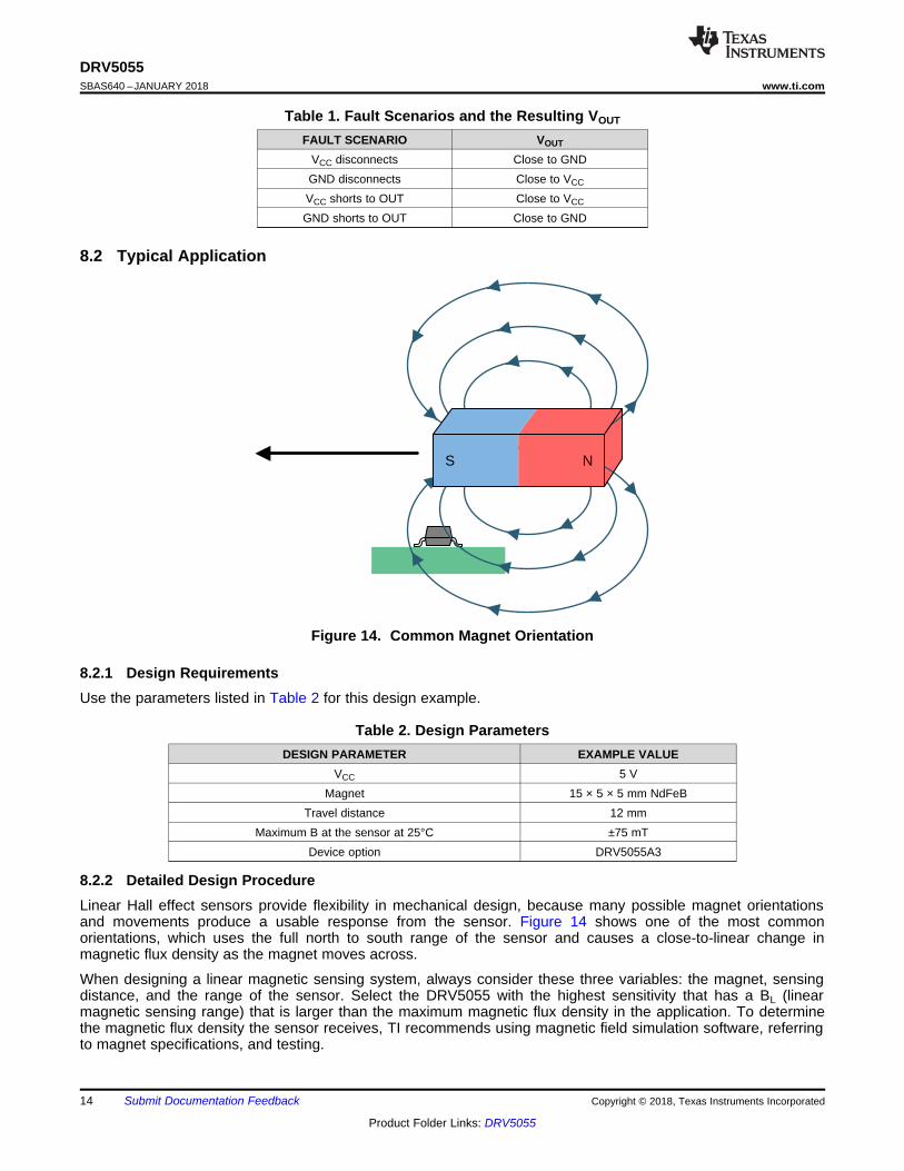
Figure 14. Common Magnet Orientation
8.2.1 Design RequirementsUse the parameters listed in Table 2 for this design example.
Table 2. Design ParametersDESIGN PARAMETER EXAMPLE VALUE
VCC 5 VMagnet 15 × 5 × 5 mm NdFeB
Travel distance 12 mmMaximum B at the sensor at 25°C ±75 mT
Device option DRV5055A3
8.2.2 Detailed Design ProcedureLinear Hall effect sensors provide flexibility in mechanical design, because many possible magnet orientationsand movements produce a usable response from the sensor. Figure 14 shows one of the most commonorientations, which uses the full north to south range of the sensor and causes a close-to-linear change inmagnetic flux density as the magnet moves across.
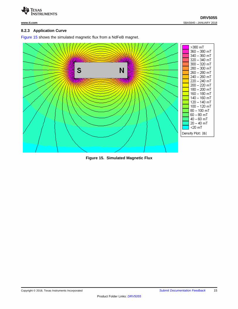
When designing a linear magnetic sensing system, always consider these three variables: the magnet, sensingdistance, and the range of the sensor. Select the DRV5055 with the highest sensitivity that has a BL (linearmagnetic sensing range) that is larger than the maximum magnetic flux density in the application. To determinethe magnetic flux density the sensor receives, TI recommends using magnetic field simulation software, referringto magnet specifications, and testing.
15
DRV5055www.ti.com SBAS640 –JANUARY 2018
Product Folder Links: DRV5055
Submit Documentation FeedbackCopyright © 2018, Texas Instruments Incorporated
8.2.3 Application CurveFigure 15 shows the simulated magnetic flux from a NdFeB magnet.
Figure 15. Simulated Magnetic Flux
CORRECT
S
N
INCORRECT
S
N
SN
SN
16
DRV5055SBAS640 –JANUARY 2018 www.ti.com
Product Folder Links: DRV5055
Submit Documentation Feedback Copyright © 2018, Texas Instruments Incorporated
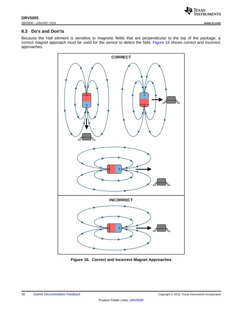
8.3 Do's and Don'tsBecause the Hall element is sensitive to magnetic fields that are perpendicular to the top of the package, acorrect magnet approach must be used for the sensor to detect the field. Figure 16 shows correct and incorrectapproaches.
Figure 16. Correct and Incorrect Magnet Approaches
GND
VCC
OUT
GND OUTVCC
17
DRV5055www.ti.com SBAS640 –JANUARY 2018
Product Folder Links: DRV5055
Submit Documentation FeedbackCopyright © 2018, Texas Instruments Incorporated
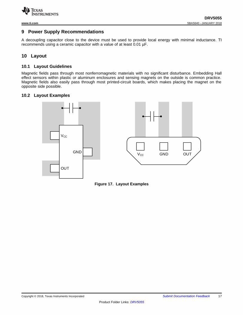
9 Power Supply RecommendationsA decoupling capacitor close to the device must be used to provide local energy with minimal inductance. TIrecommends using a ceramic capacitor with a value of at least 0.01 µF.
10 Layout
10.1 Layout GuidelinesMagnetic fields pass through most nonferromagnetic materials with no significant disturbance. Embedding Halleffect sensors within plastic or aluminum enclosures and sensing magnets on the outside is common practice.Magnetic fields also easily pass through most printed-circuit boards, which makes placing the magnet on theopposite side possible.
10.2 Layout Examples
Figure 17. Layout Examples
18
DRV5055SBAS640 –JANUARY 2018 www.ti.com
Product Folder Links: DRV5055
Submit Documentation Feedback Copyright © 2018, Texas Instruments Incorporated
11 Device and Documentation Support
11.1 Documentation Support
11.1.1 Related DocumentationFor related documentation see the following:• Using Linear Hall Effect Sensors to Measure Angle• Incremental Rotary Encoder Design Considerations
11.2 Receiving Notification of Documentation UpdatesTo receive notification of documentation updates, navigate to the device product folder on ti.com. In the upperright corner, click on Alert me to register and receive a weekly digest of any product information that haschanged. For change details, review the revision history included in any revised document.
11.3 Community ResourcesThe following links connect to TI community resources. Linked contents are provided "AS IS" by the respectivecontributors. They do not constitute TI specifications and do not necessarily reflect TI's views; see TI's Terms ofUse.
TI E2E™ Online Community TI's Engineer-to-Engineer (E2E) Community. Created to foster collaborationamong engineers. At e2e.ti.com, you can ask questions, share knowledge, explore ideas and helpsolve problems with fellow engineers.
Design Support TI's Design Support Quickly find helpful E2E forums along with design support tools andcontact information for technical support.
11.4 TrademarksE2E is a trademark of Texas Instruments.All other trademarks are the property of their respective owners.
11.5 Electrostatic Discharge CautionThis integrated circuit can be damaged by ESD. Texas Instruments recommends that all integrated circuits be handled withappropriate precautions. Failure to observe proper handling and installation procedures can cause damage.
ESD damage can range from subtle performance degradation to complete device failure. Precision integrated circuits may be moresusceptible to damage because very small parametric changes could cause the device not to meet its published specifications.
11.6 GlossarySLYZ022 — TI Glossary.
This glossary lists and explains terms, acronyms, and definitions.
12 Mechanical, Packaging, and Orderable InformationThe following pages include mechanical, packaging, and orderable information. This information is the mostcurrent data available for the designated devices. This data is subject to change without notice and revision ofthis document. For browser-based versions of this data sheet, refer to the left-hand navigation.
PACKAGE OPTION ADDENDUM
www.ti.com 3-Feb-2018
Addendum-Page 1
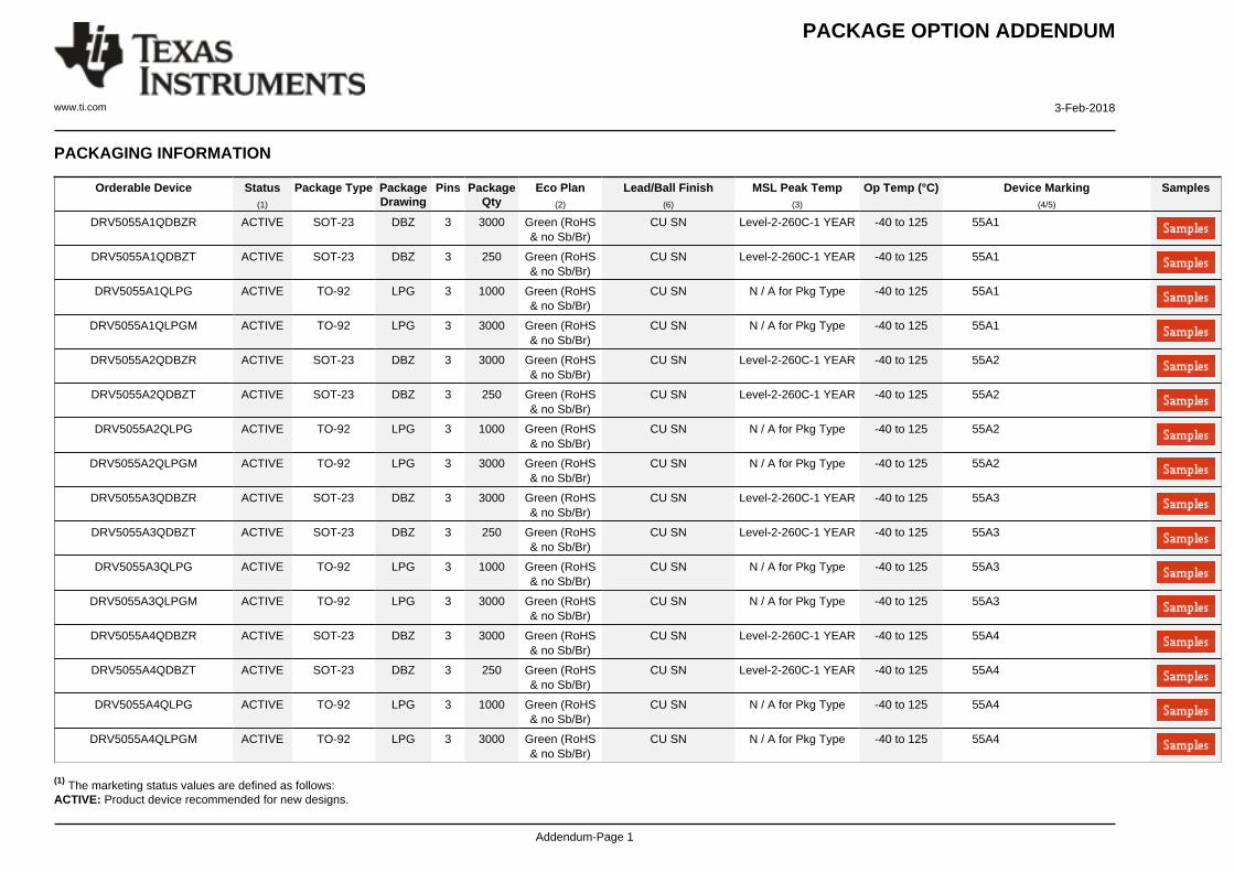
PACKAGING INFORMATION
Orderable Device Status(1)
Package Type PackageDrawing
Pins PackageQty
Eco Plan(2)
Lead/Ball Finish(6)
MSL Peak Temp(3)
Op Temp (°C) Device Marking(4/5)
Samples
DRV5055A1QDBZR ACTIVE SOT-23 DBZ 3 3000 Green (RoHS& no Sb/Br)
CU SN Level-2-260C-1 YEAR -40 to 125 55A1
DRV5055A1QDBZT ACTIVE SOT-23 DBZ 3 250 Green (RoHS& no Sb/Br)
CU SN Level-2-260C-1 YEAR -40 to 125 55A1
DRV5055A1QLPG ACTIVE TO-92 LPG 3 1000 Green (RoHS& no Sb/Br)
CU SN N / A for Pkg Type -40 to 125 55A1
DRV5055A1QLPGM ACTIVE TO-92 LPG 3 3000 Green (RoHS& no Sb/Br)
CU SN N / A for Pkg Type -40 to 125 55A1
DRV5055A2QDBZR ACTIVE SOT-23 DBZ 3 3000 Green (RoHS& no Sb/Br)
CU SN Level-2-260C-1 YEAR -40 to 125 55A2
DRV5055A2QDBZT ACTIVE SOT-23 DBZ 3 250 Green (RoHS& no Sb/Br)
CU SN Level-2-260C-1 YEAR -40 to 125 55A2
DRV5055A2QLPG ACTIVE TO-92 LPG 3 1000 Green (RoHS& no Sb/Br)
CU SN N / A for Pkg Type -40 to 125 55A2
DRV5055A2QLPGM ACTIVE TO-92 LPG 3 3000 Green (RoHS& no Sb/Br)
CU SN N / A for Pkg Type -40 to 125 55A2
DRV5055A3QDBZR ACTIVE SOT-23 DBZ 3 3000 Green (RoHS& no Sb/Br)
CU SN Level-2-260C-1 YEAR -40 to 125 55A3
DRV5055A3QDBZT ACTIVE SOT-23 DBZ 3 250 Green (RoHS& no Sb/Br)
CU SN Level-2-260C-1 YEAR -40 to 125 55A3
DRV5055A3QLPG ACTIVE TO-92 LPG 3 1000 Green (RoHS& no Sb/Br)
CU SN N / A for Pkg Type -40 to 125 55A3
DRV5055A3QLPGM ACTIVE TO-92 LPG 3 3000 Green (RoHS& no Sb/Br)
CU SN N / A for Pkg Type -40 to 125 55A3
DRV5055A4QDBZR ACTIVE SOT-23 DBZ 3 3000 Green (RoHS& no Sb/Br)
CU SN Level-2-260C-1 YEAR -40 to 125 55A4
DRV5055A4QDBZT ACTIVE SOT-23 DBZ 3 250 Green (RoHS& no Sb/Br)
CU SN Level-2-260C-1 YEAR -40 to 125 55A4
DRV5055A4QLPG ACTIVE TO-92 LPG 3 1000 Green (RoHS& no Sb/Br)
CU SN N / A for Pkg Type -40 to 125 55A4
DRV5055A4QLPGM ACTIVE TO-92 LPG 3 3000 Green (RoHS& no Sb/Br)
CU SN N / A for Pkg Type -40 to 125 55A4
(1) The marketing status values are defined as follows:ACTIVE: Product device recommended for new designs.
PACKAGE OPTION ADDENDUM
www.ti.com 3-Feb-2018
Addendum-Page 2
LIFEBUY: TI has announced that the device will be discontinued, and a lifetime-buy period is in effect.NRND: Not recommended for new designs. Device is in production to support existing customers, but TI does not recommend using this part in a new design.PREVIEW: Device has been announced but is not in production. Samples may or may not be available.OBSOLETE: TI has discontinued the production of the device.
(2) RoHS: TI defines "RoHS" to mean semiconductor products that are compliant with the current EU RoHS requirements for all 10 RoHS substances, including the requirement that RoHS substancedo not exceed 0.1% by weight in homogeneous materials. Where designed to be soldered at high temperatures, "RoHS" products are suitable for use in specified lead-free processes. TI mayreference these types of products as "Pb-Free".RoHS Exempt: TI defines "RoHS Exempt" to mean products that contain lead but are compliant with EU RoHS pursuant to a specific EU RoHS exemption.Green: TI defines "Green" to mean the content of Chlorine (Cl) and Bromine (Br) based flame retardants meet JS709B low halogen requirements of <=1000ppm threshold. Antimony trioxide basedflame retardants must also meet the <=1000ppm threshold requirement.
(3) MSL, Peak Temp. - The Moisture Sensitivity Level rating according to the JEDEC industry standard classifications, and peak solder temperature.
(4) There may be additional marking, which relates to the logo, the lot trace code information, or the environmental category on the device.
(5) Multiple Device Markings will be inside parentheses. Only one Device Marking contained in parentheses and separated by a "~" will appear on a device. If a line is indented then it is a continuationof the previous line and the two combined represent the entire Device Marking for that device.
(6) Lead/Ball Finish - Orderable Devices may have multiple material finish options. Finish options are separated by a vertical ruled line. Lead/Ball Finish values may wrap to two lines if the finishvalue exceeds the maximum column width.
Important Information and Disclaimer:The information provided on this page represents TI's knowledge and belief as of the date that it is provided. TI bases its knowledge and belief on informationprovided by third parties, and makes no representation or warranty as to the accuracy of such information. Efforts are underway to better integrate information from third parties. TI has taken andcontinues to take reasonable steps to provide representative and accurate information but may not have conducted destructive testing or chemical analysis on incoming materials and chemicals.TI and TI suppliers consider certain information to be proprietary, and thus CAS numbers and other limited information may not be available for release.
In no event shall TI's liability arising out of such information exceed the total purchase price of the TI part(s) at issue in this document sold by TI to Customer on an annual basis.
OTHER QUALIFIED VERSIONS OF DRV5055 :
• Automotive: DRV5055-Q1
NOTE: Qualified Version Definitions:
• Automotive - Q100 devices qualified for high-reliability automotive applications targeting zero defects
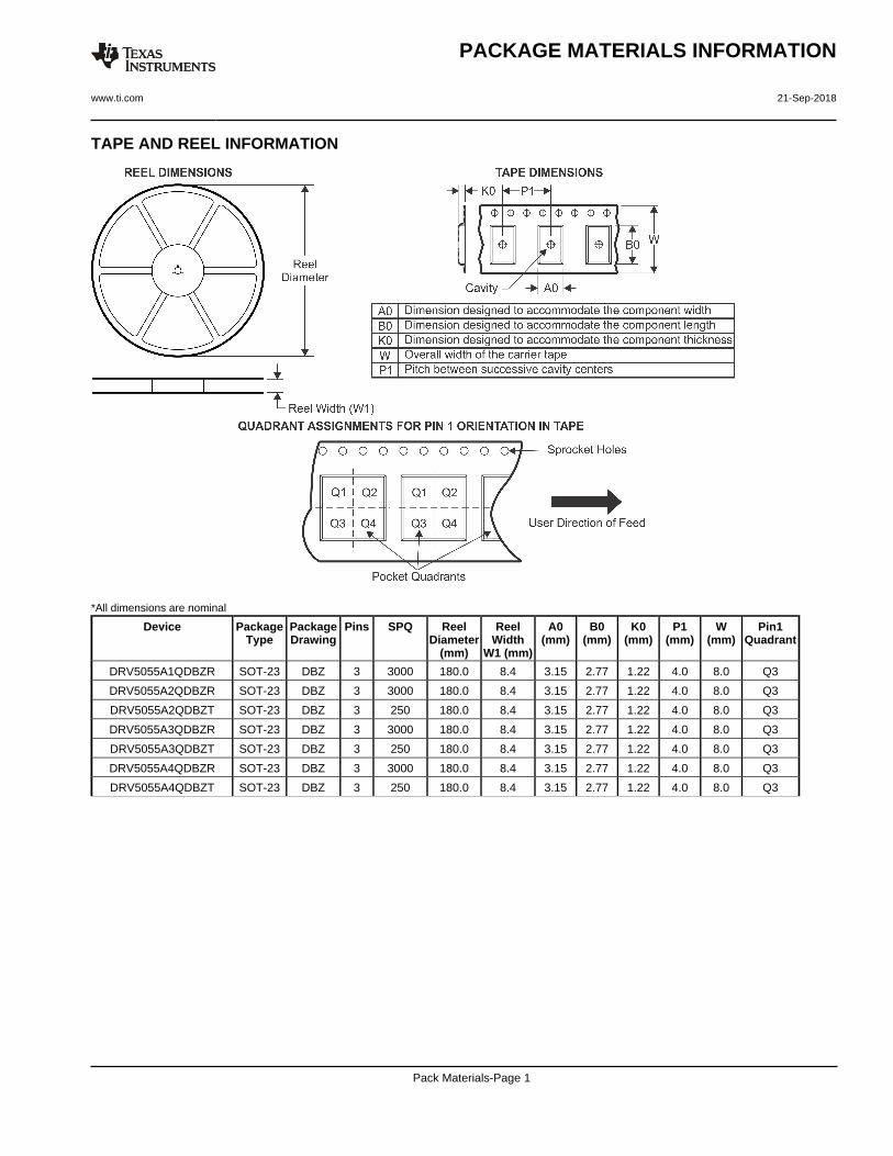
TAPE AND REEL INFORMATION
*All dimensions are nominal
Device PackageType
PackageDrawing
Pins SPQ ReelDiameter
(mm)
ReelWidth
W1 (mm)
A0(mm)
B0(mm)
K0(mm)
P1(mm)
W(mm)
Pin1Quadrant
DRV5055A1QDBZR SOT-23 DBZ 3 3000 180.0 8.4 3.15 2.77 1.22 4.0 8.0 Q3
DRV5055A2QDBZR SOT-23 DBZ 3 3000 180.0 8.4 3.15 2.77 1.22 4.0 8.0 Q3
DRV5055A2QDBZT SOT-23 DBZ 3 250 180.0 8.4 3.15 2.77 1.22 4.0 8.0 Q3
DRV5055A3QDBZR SOT-23 DBZ 3 3000 180.0 8.4 3.15 2.77 1.22 4.0 8.0 Q3
DRV5055A3QDBZT SOT-23 DBZ 3 250 180.0 8.4 3.15 2.77 1.22 4.0 8.0 Q3
DRV5055A4QDBZR SOT-23 DBZ 3 3000 180.0 8.4 3.15 2.77 1.22 4.0 8.0 Q3
DRV5055A4QDBZT SOT-23 DBZ 3 250 180.0 8.4 3.15 2.77 1.22 4.0 8.0 Q3
PACKAGE MATERIALS INFORMATION
www.ti.com 21-Sep-2018
Pack Materials-Page 1
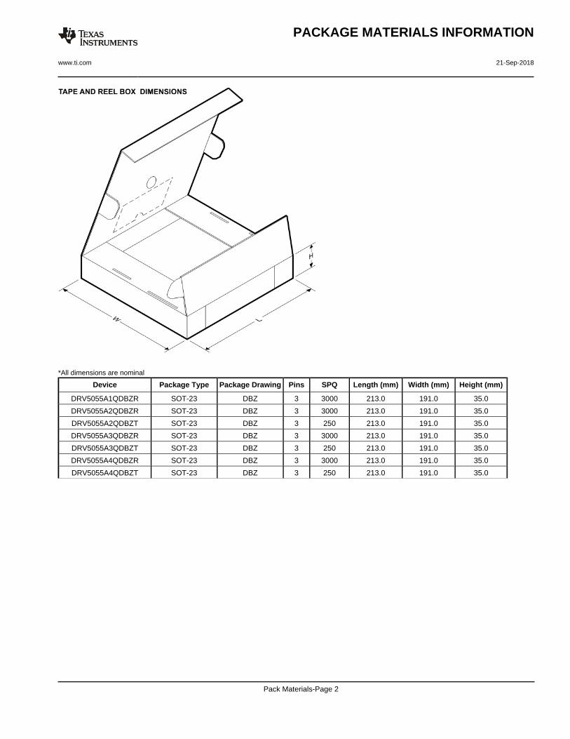
*All dimensions are nominal
Device Package Type Package Drawing Pins SPQ Length (mm) Width (mm) Height (mm)
DRV5055A1QDBZR SOT-23 DBZ 3 3000 213.0 191.0 35.0
DRV5055A2QDBZR SOT-23 DBZ 3 3000 213.0 191.0 35.0
DRV5055A2QDBZT SOT-23 DBZ 3 250 213.0 191.0 35.0
DRV5055A3QDBZR SOT-23 DBZ 3 3000 213.0 191.0 35.0
DRV5055A3QDBZT SOT-23 DBZ 3 250 213.0 191.0 35.0
DRV5055A4QDBZR SOT-23 DBZ 3 3000 213.0 191.0 35.0
DRV5055A4QDBZT SOT-23 DBZ 3 250 213.0 191.0 35.0
PACKAGE MATERIALS INFORMATION
www.ti.com 21-Sep-2018
Pack Materials-Page 2
4203227/C
www.ti.com
PACKAGE OUTLINE
C
TYP0.200.08
0.25
2.642.10
1.12 MAX
TYP0.100.01
3X 0.50.3
TYP0.60.2
1.9
0.95
TYP-80
A
3.042.80
B1.41.2
(0.95)
SOT-23 - 1.12 mm max heightDBZ0003ASMALL OUTLINE TRANSISTOR
4214838/C 04/2017
NOTES: 1. All linear dimensions are in millimeters. Any dimensions in parenthesis are for reference only. Dimensioning and tolerancing per ASME Y14.5M.2. This drawing is subject to change without notice.3. Reference JEDEC registration TO-236, except minimum foot length.
0.2 C A B
1
3
2
INDEX AREAPIN 1
GAGE PLANE
SEATING PLANE
0.1 C
SCALE 4.000
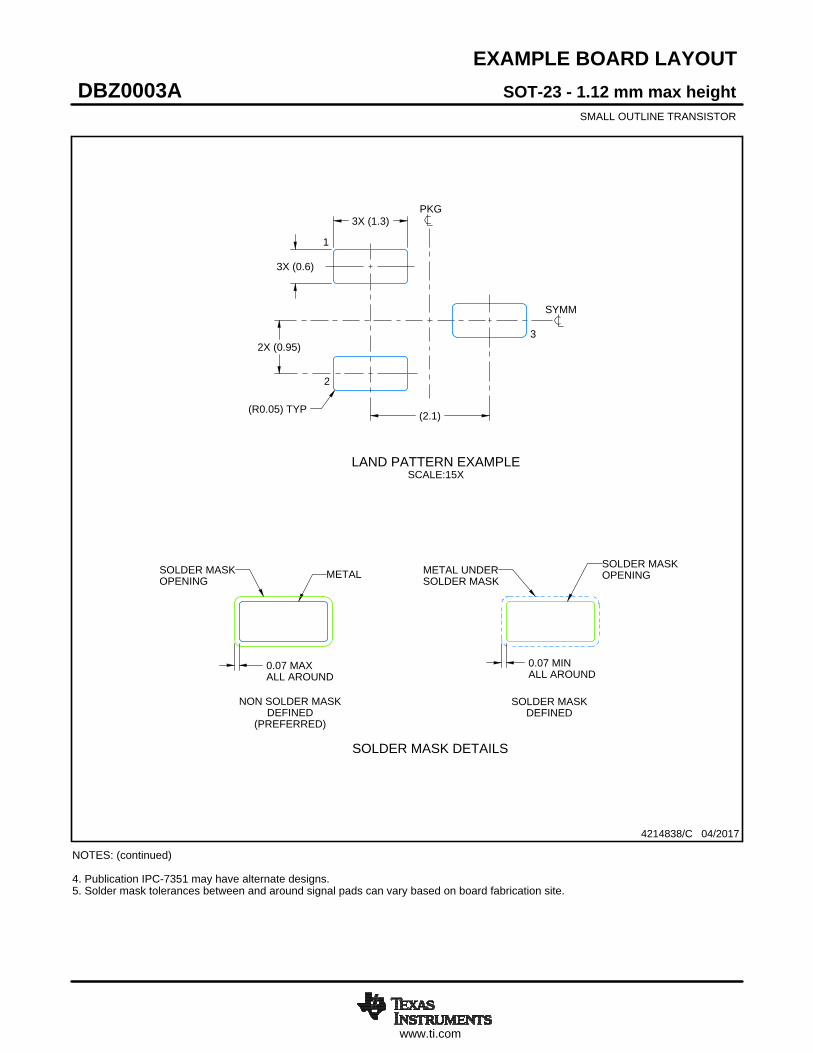
www.ti.com
EXAMPLE BOARD LAYOUT
0.07 MAXALL AROUND
0.07 MINALL AROUND
3X (1.3)
3X (0.6)
(2.1)
2X (0.95)
(R0.05) TYP
4214838/C 04/2017
SOT-23 - 1.12 mm max heightDBZ0003ASMALL OUTLINE TRANSISTOR
NOTES: (continued) 4. Publication IPC-7351 may have alternate designs. 5. Solder mask tolerances between and around signal pads can vary based on board fabrication site.
SYMM
LAND PATTERN EXAMPLESCALE:15X
PKG
1
3
2
SOLDER MASKOPENINGMETAL UNDER
SOLDER MASK
SOLDER MASKDEFINED
METALSOLDER MASKOPENING
NON SOLDER MASKDEFINED
(PREFERRED)
SOLDER MASK DETAILS
www.ti.com
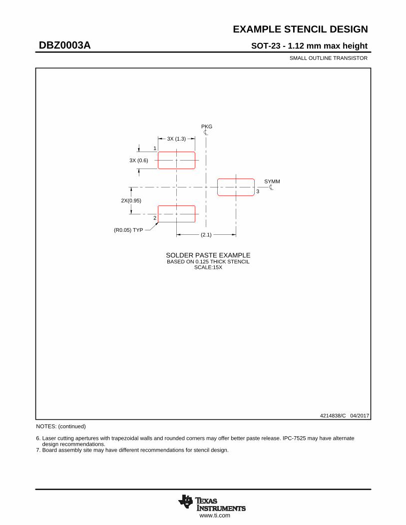
EXAMPLE STENCIL DESIGN
(2.1)
2X(0.95)
3X (1.3)
3X (0.6)
(R0.05) TYP
SOT-23 - 1.12 mm max heightDBZ0003ASMALL OUTLINE TRANSISTOR
4214838/C 04/2017
NOTES: (continued) 6. Laser cutting apertures with trapezoidal walls and rounded corners may offer better paste release. IPC-7525 may have alternate design recommendations. 7. Board assembly site may have different recommendations for stencil design.
SOLDER PASTE EXAMPLEBASED ON 0.125 THICK STENCIL
SCALE:15X
SYMM
PKG
1
3
2
www.ti.com
PACKAGE OUTLINE
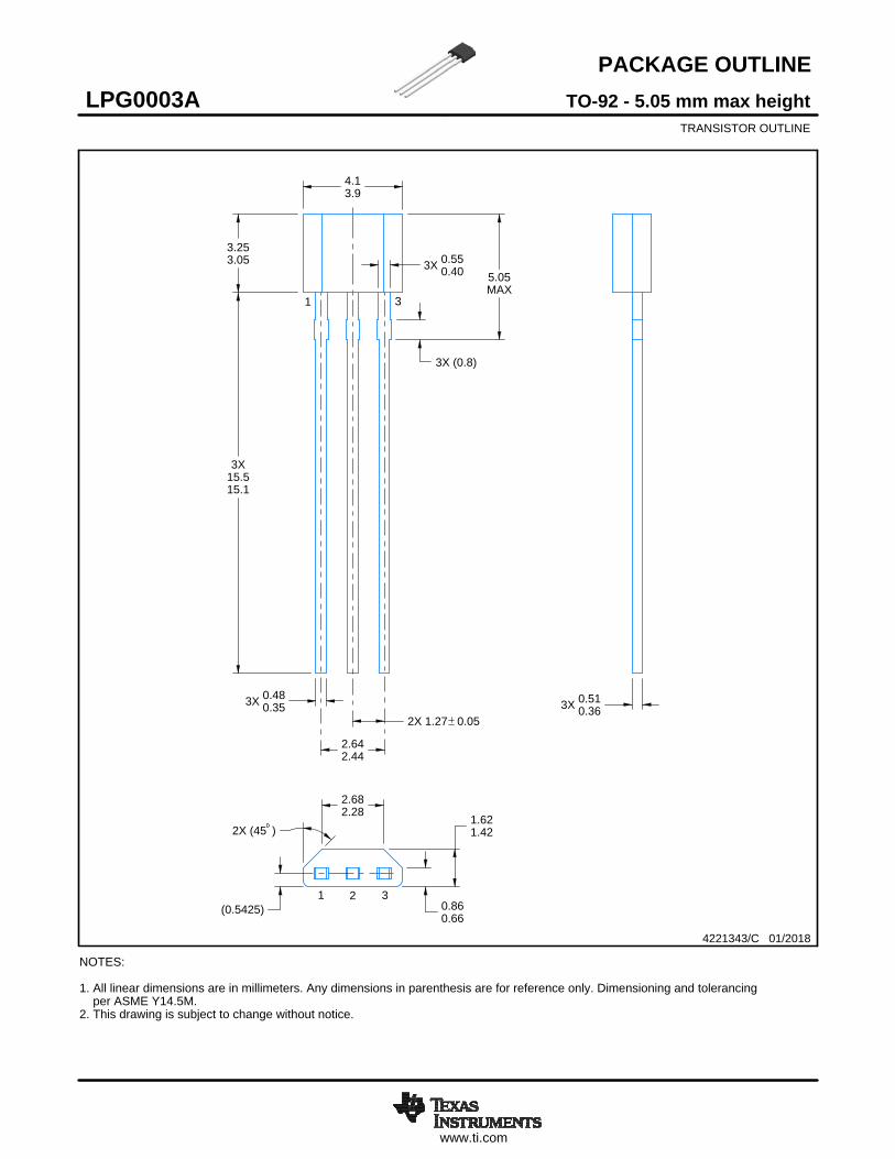
4.13.9
3X15.515.1
3X 0.480.35
2X 1.27 0.05
3.253.05
3X 0.510.36
3X 0.550.40
2X (45 )
0.860.66
1.621.42
2.642.44
2.682.28
5.05MAX
(0.5425)
3X (0.8)
4221343/C 01/2018
TO-92 - 5.05 mm max heightLPG0003ATRANSISTOR OUTLINE
NOTES: 1. All linear dimensions are in millimeters. Any dimensions in parenthesis are for reference only. Dimensioning and tolerancing per ASME Y14.5M.2. This drawing is subject to change without notice.
1 3
1 2 3
SCALE 1.300
www.ti.com
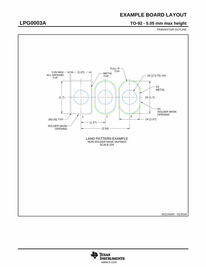
EXAMPLE BOARD LAYOUT
TYP ALL AROUND
0.05 MAXFULL R
TYP(1.07)
(1.7)
(1.27)
(2.54)
(R0.05) TYP 2X (1.07)
2X (1.7)
3X ( 0.75) VIA
4221343/C 01/2018
TO-92 - 5.05 mm max heightLPG0003ATRANSISTOR OUTLINE
LAND PATTERN EXAMPLENON-SOLDER MASK DEFINED
SCALE:20X
METALTYP
OPENINGSOLDER MASK
1 32
2XMETAL
2XSOLDER MASKOPENING
www.ti.com
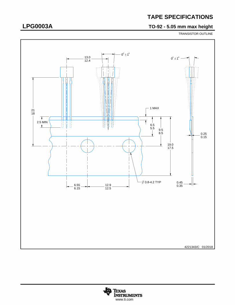
TAPE SPECIFICATIONS
0 10 1
12.912.5
6.556.15
13.012.4
2.5 MIN6.55.5
3.8-4.2 TYP
9.58.5
19.017.5
1 MAX2118
0.450.35
0.250.15
TO-92 - 5.05 mm max heightLPG0003ATRANSISTOR OUTLINE
4221343/C 01/2018

IMPORTANT NOTICE AND DISCLAIMER
TI PROVIDES TECHNICAL AND RELIABILITY DATA (INCLUDING DATASHEETS), DESIGN RESOURCES (INCLUDING REFERENCEDESIGNS), APPLICATION OR OTHER DESIGN ADVICE, WEB TOOLS, SAFETY INFORMATION, AND OTHER RESOURCES “AS IS”AND WITH ALL FAULTS, AND DISCLAIMS ALL WARRANTIES, EXPRESS AND IMPLIED, INCLUDING WITHOUT LIMITATION ANYIMPLIED WARRANTIES OF MERCHANTABILITY, FITNESS FOR A PARTICULAR PURPOSE OR NON-INFRINGEMENT OF THIRDPARTY INTELLECTUAL PROPERTY RIGHTS.These resources are intended for skilled developers designing with TI products. You are solely responsible for (1) selecting the appropriateTI products for your application, (2) designing, validating and testing your application, and (3) ensuring your application meets applicablestandards, and any other safety, security, or other requirements. These resources are subject to change without notice. TI grants youpermission to use these resources only for development of an application that uses the TI products described in the resource. Otherreproduction and display of these resources is prohibited. No license is granted to any other TI intellectual property right or to any thirdparty intellectual property right. TI disclaims responsibility for, and you will fully indemnify TI and its representatives against, any claims,damages, costs, losses, and liabilities arising out of your use of these resources.TI’s products are provided subject to TI’s Terms of Sale (www.ti.com/legal/termsofsale.html) or other applicable terms available either onti.com or provided in conjunction with such TI products. TI’s provision of these resources does not expand or otherwise alter TI’s applicablewarranties or warranty disclaimers for TI products.
Mailing Address: Texas Instruments, Post Office Box 655303, Dallas, Texas 75265Copyright © 2018, Texas Instruments Incorporated