Embed Size (px)
Citation preview
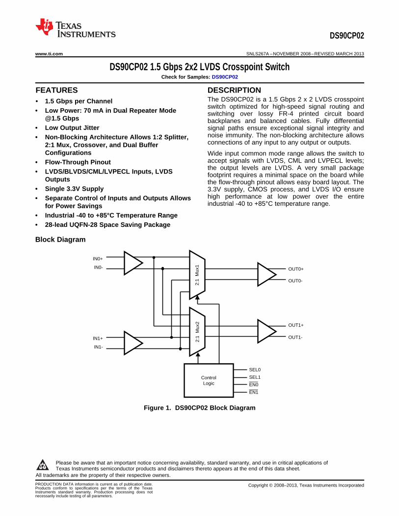
OUT0+
SEL0
OUT0-
OUT1+
OUT1-
SEL1
EN0
2:1
Mux
22:
1 M
ux1
IN1-
IN1+
IN0-
IN0+
EN1
ControlLogic
DS90CP02
www.ti.com SNLS267A –NOVEMBER 2008–REVISED MARCH 2013
DS90CP02 1.5 Gbps 2x2 LVDS Crosspoint SwitchCheck for Samples: DS90CP02
1FEATURES DESCRIPTIONThe DS90CP02 is a 1.5 Gbps 2 x 2 LVDS crosspoint
2• 1.5 Gbps per Channelswitch optimized for high-speed signal routing and
• Low Power: 70 mA in Dual Repeater Mode switching over lossy FR-4 printed circuit [email protected] Gbps backplanes and balanced cables. Fully differential
• Low Output Jitter signal paths ensure exceptional signal integrity andnoise immunity. The non-blocking architecture allows• Non-Blocking Architecture Allows 1:2 Splitter,connections of any input to any output or outputs.2:1 Mux, Crossover, and Dual Buffer
Configurations Wide input common mode range allows the switch toaccept signals with LVDS, CML and LVPECL levels;• Flow-Through Pinoutthe output levels are LVDS. A very small package• LVDS/BLVDS/CML/LVPECL Inputs, LVDS footprint requires a minimal space on the board while
Outputs the flow-through pinout allows easy board layout. The• Single 3.3V Supply 3.3V supply, CMOS process, and LVDS I/O ensure
high performance at low power over the entire• Separate Control of Inputs and Outputs Allowsindustrial -40 to +85°C temperature range.for Power Savings
• Industrial -40 to +85°C Temperature Range• 28-lead UQFN-28 Space Saving Package
Block Diagram
Figure 1. DS90CP02 Block Diagram
1
Please be aware that an important notice concerning availability, standard warranty, and use in critical applications ofTexas Instruments semiconductor products and disclaimers thereto appears at the end of this data sheet.
2All trademarks are the property of their respective owners.
PRODUCTION DATA information is current as of publication date. Copyright © 2008–2013, Texas Instruments IncorporatedProducts conform to specifications per the terms of the TexasInstruments standard warranty. Production processing does notnecessarily include testing of all parameters.
7 6 5 4 3 2 1
15 16 17 18 19 20 21
28
27
26
25
24
23
22
8
9
10
11
12
13
14
EN
0
SE
L0
SE
L1
GN
D
GN
D
GN
D
GN
D
N/C
IN0+
IN0-
VDDA
IN1+
IN1-
VDD
EN
1
VD
D
GN
D
VD
D
VD
D
N/C
GN
D
N/C
OUT0+
OUT0-
VDDA
OUT1+
OUT1-
VDD
DAP(GND)
DS90CP02
SNLS267A –NOVEMBER 2008–REVISED MARCH 2013 www.ti.com
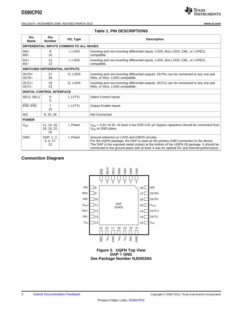
Table 1. PIN DESCRIPTIONS
Pin Pin I/O, Type DescriptionName Number
DIFFERENTIAL INPUTS COMMON TO ALL MUXES
IN0+ 9 I, LVDS Inverting and non-inverting differential inputs. LVDS, Bus LVDS, CML, or LVPECLIN0− 10 compatible.
IN1+ 12 I, LVDS Inverting and non-inverting differential inputs. LVDS, Bus LVDS, CML, or LVPECLIN1− 13 compatible.
SWITCHED DIFFERENTIAL OUTPUTS
OUT0+ 27 O, LVDS Inverting and non-inverting differential outputs. OUT0± can be connected to any one pairOUT0− 26 IN0±, or IN1±. LVDS compatible .
OUT1+ 24 O, LVDS Inverting and non-inverting differential outputs. OUT1± can be connected to any one pairOUT1− 23 IN0±, or IN1±. LVDS compatible .
DIGITAL CONTROL INTERFACE
SEL0, SEL1 6 I, LVTTL Select Control Inputs5
EN0, EN1 7 I, LVTTL Output Enable Inputs15
N/C 8, 20, 28 Not Connected
POWER
VDD 11, 14, 16, I, Power VDD = 3.3V ±0.3V. At least 4 low ESR 0.01 µF bypass capacitors should be connected from18, 19, 22, VDD to GND plane.
25
GND DAP, 1, 2, I, Power Ground reference to LVDS and CMOS circuitry.3, 4, 17, For the UQFN package, the DAP is used as the primary GND connection to the device.
21 The DAP is the exposed metal contact at the bottom of the UQFN-28 package. It should beconnected to the ground plane with at least 4 vias for optimal AC and thermal performance.
Connection Diagram
Figure 2. UQFN Top ViewDAP = GND
See Package Number NJD0028A
2 Submit Documentation Feedback Copyright © 2008–2013, Texas Instruments Incorporated
Product Folder Links: DS90CP02
DS90CP02
www.ti.com SNLS267A –NOVEMBER 2008–REVISED MARCH 2013
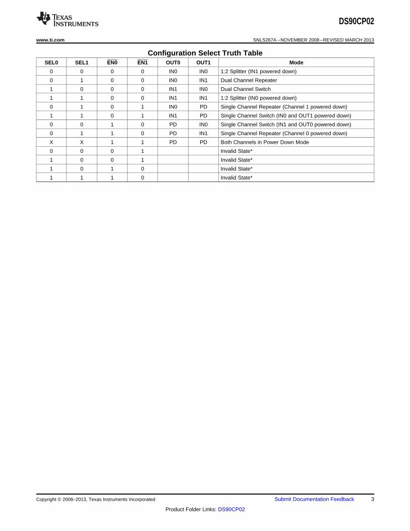
Configuration Select Truth TableSEL0 SEL1 EN0 EN1 OUT0 OUT1 Mode
0 0 0 0 IN0 IN0 1:2 Splitter (IN1 powered down)
0 1 0 0 IN0 IN1 Dual Channel Repeater
1 0 0 0 IN1 IN0 Dual Channel Switch
1 1 0 0 IN1 IN1 1:2 Splitter (IN0 powered down)
0 1 0 1 IN0 PD Single Channel Repeater (Channel 1 powered down)
1 1 0 1 IN1 PD Single Channel Switch (IN0 and OUT1 powered down)
0 0 1 0 PD IN0 Single Channel Switch (IN1 and OUT0 powered down)
0 1 1 0 PD IN1 Single Channel Repeater (Channel 0 powered down)
X X 1 1 PD PD Both Channels in Power Down Mode
0 0 0 1 Invalid State*
1 0 0 1 Invalid State*
1 0 1 0 Invalid State*
1 1 1 0 Invalid State*
Copyright © 2008–2013, Texas Instruments Incorporated Submit Documentation Feedback 3
Product Folder Links: DS90CP02
Single Channel Repeater
(SEL0=0, SEL1=1, =1, =0)EN0 EN1
OUT0+
OUT0-
OUT1+
OUT1-
IN0-
IN0+
IN1-
IN1+
OUT0+
OUT0-
OUT1+
OUT1-
IN0-
IN0+
IN1-
IN1+
Single Channel Crossover Switch
(SEL0=1, SEL1=1, =0, =1)EN0 EN1
Single Channel Repeater
(SEL0=0, SEL1=1, =0, =1)EN0 EN1
OUT0+
OUT0-
OUT1+
OUT1-
IN0-
IN0+
IN1-
IN1+
OUT0+
OUT0-
OUT1+
OUT1-
IN0-
IN0+
IN1-
IN1+
Single Channel Crossover Switch
(SEL0=0, SEL1=0, =1, =0)EN0 EN1
1:2 Splitter
(SEL0=1, SEL1=1, =0, =0)EN0 EN1
Dual Channel Switch
(SEL0=1, SEL1=0, =0, =0)EN0 EN1
OUT0+
OUT0-
OUT1+
OUT1-
IN0-
IN0+
IN1-
IN1+
OUT0+
OUT0-
OUT1+
OUT1-
IN0-
IN0+
IN1-
IN1+
Dual Channel Repeater
(SEL0=0, SEL1=1, =0, =0)EN0 EN1
1:2 Splitter
(SEL0=0, SEL1=0, =0, =0)EN0 EN1
OUT0+
OUT0-
OUT1+
OUT1-
IN0-
IN0+
IN1-
IN1+
OUT0+
OUT0-
OUT1+
OUT1-
IN0-
IN0+
IN1-
IN1+
DS90CP02
SNLS267A –NOVEMBER 2008–REVISED MARCH 2013 www.ti.com
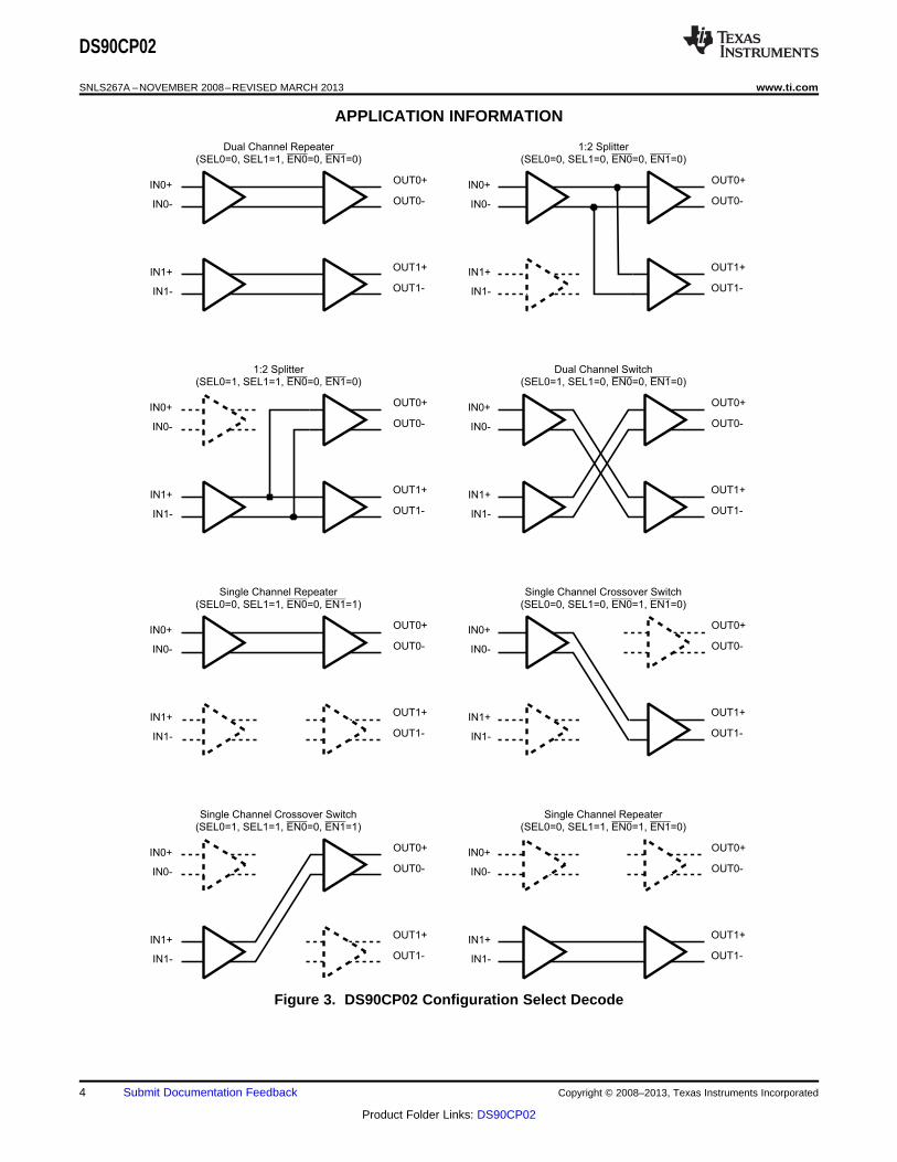
APPLICATION INFORMATION
Figure 3. DS90CP02 Configuration Select Decode
4 Submit Documentation Feedback Copyright © 2008–2013, Texas Instruments Incorporated
Product Folder Links: DS90CP02
DS90CP02
www.ti.com SNLS267A –NOVEMBER 2008–REVISED MARCH 2013
These devices have limited built-in ESD protection. The leads should be shorted together or the device placed in conductive foamduring storage or handling to prevent electrostatic damage to the MOS gates.
Absolute Maximum Ratings (1) (2)
Supply Voltage (VDD) −0.3V to +4.0V
CMOS Input Voltage −0.3V to (VDD +0.3V)
LVDS Receiver Input Voltage −0.3V to +3.6V
LVDS Driver Output Voltage −0.3V to +3.6V
LVDS Output Short Circuit Current 40mA
Junction Temperature +150°C
Storage Temperature −65°C to +150°C
Lead Temperature(Soldering, 4sec.) +260°C
Maximum Package Power Dissipation at 25°C
UQFN-28 4.31 W
Derating above 25°C
UQFN-28 34.5 mW/°C
Thermal Resistance, θJA
UQFN-28 29°C/W
ESD Rating
HBM, 1.5 kΩ, 100 pF 6.5 kV
EIAJ, 0Ω, 200 pF >250V
(1) “Absolute Maximum Ratings” are the ratings beyond which the safety of the device cannot be guaranteed. They are not meant to implythat the device should be operated at these limits.
(2) If Military/Aerospace specified devices are required, please contact the Texas Instruments Sales Office/Distributors for availability andspecifications.
Recommended Operating ConditionsMin Typ Max Unit
Supply Voltage (VDD– GND) 3.0 3.3 3.6 V
Receiver Input Voltage 0 3.6 V
Operating Free Air Temperature −40 25 85 °C
Junction Temperature 150 °C
Copyright © 2008–2013, Texas Instruments Incorporated Submit Documentation Feedback 5
Product Folder Links: DS90CP02
DS90CP02
SNLS267A –NOVEMBER 2008–REVISED MARCH 2013 www.ti.com
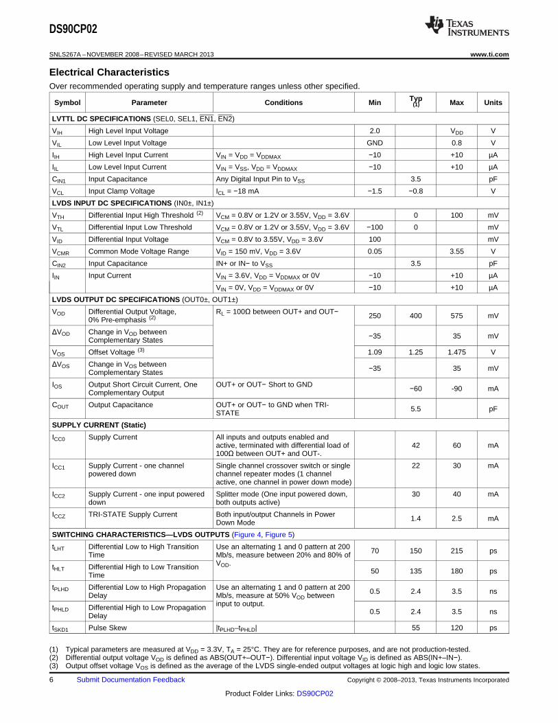
Electrical CharacteristicsOver recommended operating supply and temperature ranges unless other specified.
TypSymbol Parameter Conditions Min Max Units(1)
LVTTL DC SPECIFICATIONS (SEL0, SEL1, EN1, EN2)
VIH High Level Input Voltage 2.0 VDD V
VIL Low Level Input Voltage GND 0.8 V
IIH High Level Input Current VIN = VDD = VDDMAX −10 +10 µA
IIL Low Level Input Current VIN = VSS, VDD = VDDMAX −10 +10 µA
CIN1 Input Capacitance Any Digital Input Pin to VSS 3.5 pF
VCL Input Clamp Voltage ICL = −18 mA −1.5 −0.8 V
LVDS INPUT DC SPECIFICATIONS (IN0±, IN1±)
VTH Differential Input High Threshold (2) VCM = 0.8V or 1.2V or 3.55V, VDD = 3.6V 0 100 mV
VTL Differential Input Low Threshold VCM = 0.8V or 1.2V or 3.55V, VDD = 3.6V −100 0 mV
VID Differential Input Voltage VCM = 0.8V to 3.55V, VDD = 3.6V 100 mV
VCMR Common Mode Voltage Range VID = 150 mV, VDD = 3.6V 0.05 3.55 V
CIN2 Input Capacitance IN+ or IN− to VSS 3.5 pF
IIN Input Current VIN = 3.6V, VDD = VDDMAX or 0V −10 +10 µA
VIN = 0V, VDD = VDDMAX or 0V −10 +10 µA
LVDS OUTPUT DC SPECIFICATIONS (OUT0±, OUT1±)
VOD Differential Output Voltage, RL = 100Ω between OUT+ and OUT− 250 400 575 mV0% Pre-emphasis (2)
ΔVOD Change in VOD between −35 35 mVComplementary States
VOS Offset Voltage (3) 1.09 1.25 1.475 V
ΔVOS Change in VOS between −35 35 mVComplementary States
IOS Output Short Circuit Current, One OUT+ or OUT− Short to GND −60 -90 mAComplementary Output
COUT Output Capacitance OUT+ or OUT− to GND when TRI- 5.5 pFSTATE
SUPPLY CURRENT (Static)
ICC0 Supply Current All inputs and outputs enabled andactive, terminated with differential load of 42 60 mA100Ω between OUT+ and OUT-.
ICC1 Supply Current - one channel Single channel crossover switch or single 22 30 mApowered down channel repeater modes (1 channel
active, one channel in power down mode)
ICC2 Supply Current - one input powered Splitter mode (One input powered down, 30 40 mAdown both outputs active)
ICCZ TRI-STATE Supply Current Both input/output Channels in Power 1.4 2.5 mADown Mode
SWITCHING CHARACTERISTICS—LVDS OUTPUTS (Figure 4, Figure 5)
tLHT Differential Low to High Transition Use an alternating 1 and 0 pattern at 200 70 150 215 psTime Mb/s, measure between 20% and 80% ofVOD.tHLT Differential High to Low Transition 50 135 180 psTime
tPLHD Differential Low to High Propagation Use an alternating 1 and 0 pattern at 200 0.5 2.4 3.5 nsDelay Mb/s, measure at 50% VOD betweeninput to output.tPHLD Differential High to Low Propagation 0.5 2.4 3.5 nsDelay
tSKD1 Pulse Skew |tPLHD–tPHLD| 55 120 ps
(1) Typical parameters are measured at VDD = 3.3V, TA = 25°C. They are for reference purposes, and are not production-tested.(2) Differential output voltage VOD is defined as ABS(OUT+–OUT−). Differential input voltage VID is defined as ABS(IN+–IN−).(3) Output offset voltage VOS is defined as the average of the LVDS single-ended output voltages at logic high and logic low states.
6 Submit Documentation Feedback Copyright © 2008–2013, Texas Instruments Incorporated
Product Folder Links: DS90CP02
DS90CP02
www.ti.com SNLS267A –NOVEMBER 2008–REVISED MARCH 2013
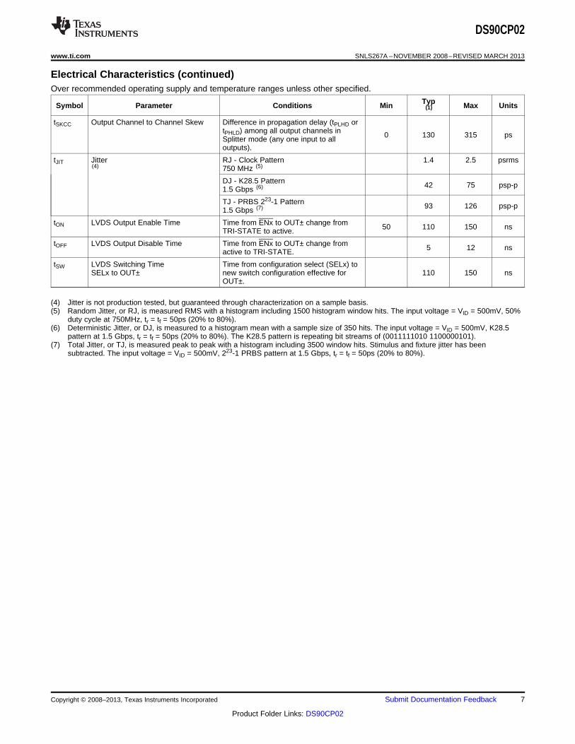
Electrical Characteristics (continued)Over recommended operating supply and temperature ranges unless other specified.
TypSymbol Parameter Conditions Min Max Units(1)
tSKCC Output Channel to Channel Skew Difference in propagation delay (tPLHD ortPHLD) among all output channels in 0 130 315 psSplitter mode (any one input to alloutputs).
tJIT Jitter RJ - Clock Pattern 1.4 2.5 psrms(4) 750 MHz (5)
DJ - K28.5 Pattern 42 75 psp-p1.5 Gbps (6)
TJ - PRBS 223-1 Pattern 93 126 psp-p1.5 Gbps (7)
tON LVDS Output Enable Time Time from ENx to OUT± change from 50 110 150 nsTRI-STATE to active.
tOFF LVDS Output Disable Time Time from ENx to OUT± change from 5 12 nsactive to TRI-STATE.
tSW LVDS Switching Time Time from configuration select (SELx) toSELx to OUT± new switch configuration effective for 110 150 ns
OUT±.
(4) Jitter is not production tested, but guaranteed through characterization on a sample basis.(5) Random Jitter, or RJ, is measured RMS with a histogram including 1500 histogram window hits. The input voltage = VID = 500mV, 50%
duty cycle at 750MHz, tr = tf = 50ps (20% to 80%).(6) Deterministic Jitter, or DJ, is measured to a histogram mean with a sample size of 350 hits. The input voltage = VID = 500mV, K28.5
pattern at 1.5 Gbps, tr = tf = 50ps (20% to 80%). The K28.5 pattern is repeating bit streams of (0011111010 1100000101).(7) Total Jitter, or TJ, is measured peak to peak with a histogram including 3500 window hits. Stimulus and fixture jitter has been
subtracted. The input voltage = VID = 500mV, 223-1 PRBS pattern at 1.5 Gbps, tr = tf = 50ps (20% to 80%).
Copyright © 2008–2013, Texas Instruments Incorporated Submit Documentation Feedback 7
Product Folder Links: DS90CP02
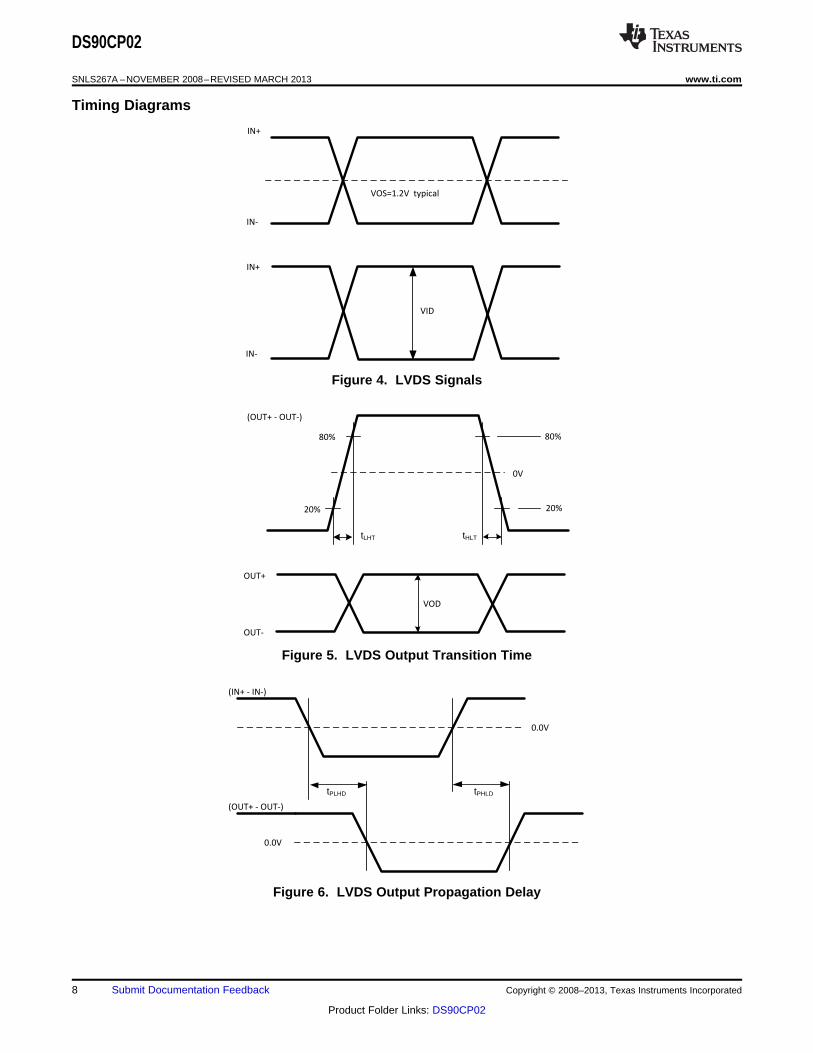
(IN+ - IN-)
(OUT+ - OUT-)
0.0V
0.0V
tPLHD tPHLD
80%
20%
0V
80%
20%
tLHT tHLT
VOD
OUT-
OUT+
(OUT+ - OUT-)
IN+
IN-
VOS=1.2V typical
VID
IN-
IN+
DS90CP02
SNLS267A –NOVEMBER 2008–REVISED MARCH 2013 www.ti.com
Timing Diagrams
Figure 4. LVDS Signals
Figure 5. LVDS Output Transition Time
Figure 6. LVDS Output Propagation Delay
8 Submit Documentation Feedback Copyright © 2008–2013, Texas Instruments Incorporated
Product Folder Links: DS90CP02
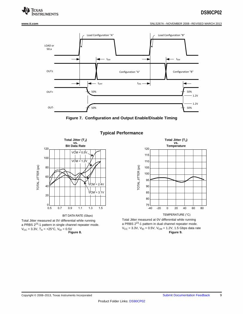
TO
TA
LJIT
TE
R (
ps)
120
0
BIT DATA RATE (Gbps)
0.5 0.7 0.9 1.3 1.5
20
40
60
80
100
VCM = 0.5V
VCM = 1.2V
VCM = 3.1V
VCM = 2.4V
1.1
TO
TA
LJIT
TE
R (
ps)
120
75
TEMPERATURE (°C)
-40 -20 0 40 60
80
85
90
105
110
95
100
115
8020
tOFF
LOAD or
SELx
1.2V
OUT±
1.2V
50%
50%
50%
50%OUT+
OUT-
tSW tSW
tON
Load Configuration "A" Load Configuration "B"
Configuration "A" Configuration "B"
DS90CP02
www.ti.com SNLS267A –NOVEMBER 2008–REVISED MARCH 2013
Figure 7. Configuration and Output Enable/Disable Timing
Typical Performance
Total Jitter (TJ) Total Jitter (TJ)vs. vs.
Bit Data Rate Temperature
Total Jitter measured at 0V differential while runningTotal Jitter measured at 0V differential while runninga PRBS 223-1 pattern in dual channel repeater mode.a PRBS 223-1 pattern in single channel repeater mode.VCC = 3.3V, VID = 0.5V, VCM = 1.2V, 1.5 Gbps data rateVCC = 3.3V, TA = +25°C, VID = 0.5V
Figure 8. Figure 9.
Copyright © 2008–2013, Texas Instruments Incorporated Submit Documentation Feedback 9
Product Folder Links: DS90CP02
DS90CP02
SNLS267A –NOVEMBER 2008–REVISED MARCH 2013 www.ti.com
REVISION HISTORY
Changes from Original (March 2013) to Revision A Page
• Changed layout of National Data Sheet to TI format ............................................................................................................ 9
10 Submit Documentation Feedback Copyright © 2008–2013, Texas Instruments Incorporated
Product Folder Links: DS90CP02
PACKAGE OPTION ADDENDUM
www.ti.com 10-Dec-2020
Addendum-Page 1
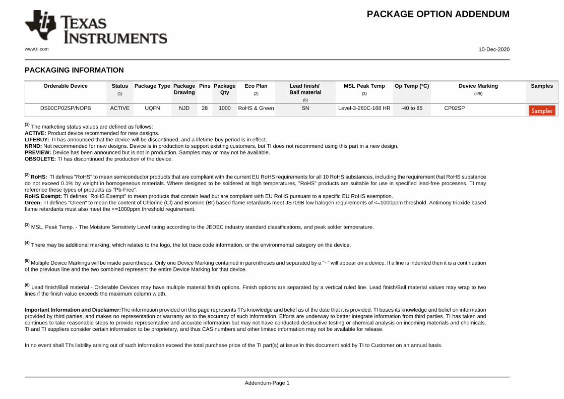
PACKAGING INFORMATION
Orderable Device Status(1)
Package Type PackageDrawing
Pins PackageQty
Eco Plan(2)
Lead finish/Ball material
(6)
MSL Peak Temp(3)
Op Temp (°C) Device Marking(4/5)
Samples
DS90CP02SP/NOPB ACTIVE UQFN NJD 28 1000 RoHS & Green SN Level-3-260C-168 HR -40 to 85 CP02SP
(1) The marketing status values are defined as follows:ACTIVE: Product device recommended for new designs.LIFEBUY: TI has announced that the device will be discontinued, and a lifetime-buy period is in effect.NRND: Not recommended for new designs. Device is in production to support existing customers, but TI does not recommend using this part in a new design.PREVIEW: Device has been announced but is not in production. Samples may or may not be available.OBSOLETE: TI has discontinued the production of the device.
(2) RoHS: TI defines "RoHS" to mean semiconductor products that are compliant with the current EU RoHS requirements for all 10 RoHS substances, including the requirement that RoHS substancedo not exceed 0.1% by weight in homogeneous materials. Where designed to be soldered at high temperatures, "RoHS" products are suitable for use in specified lead-free processes. TI mayreference these types of products as "Pb-Free".RoHS Exempt: TI defines "RoHS Exempt" to mean products that contain lead but are compliant with EU RoHS pursuant to a specific EU RoHS exemption.Green: TI defines "Green" to mean the content of Chlorine (Cl) and Bromine (Br) based flame retardants meet JS709B low halogen requirements of <=1000ppm threshold. Antimony trioxide basedflame retardants must also meet the <=1000ppm threshold requirement.
(3) MSL, Peak Temp. - The Moisture Sensitivity Level rating according to the JEDEC industry standard classifications, and peak solder temperature.
(4) There may be additional marking, which relates to the logo, the lot trace code information, or the environmental category on the device.
(5) Multiple Device Markings will be inside parentheses. Only one Device Marking contained in parentheses and separated by a "~" will appear on a device. If a line is indented then it is a continuationof the previous line and the two combined represent the entire Device Marking for that device.
(6) Lead finish/Ball material - Orderable Devices may have multiple material finish options. Finish options are separated by a vertical ruled line. Lead finish/Ball material values may wrap to twolines if the finish value exceeds the maximum column width.
Important Information and Disclaimer:The information provided on this page represents TI's knowledge and belief as of the date that it is provided. TI bases its knowledge and belief on informationprovided by third parties, and makes no representation or warranty as to the accuracy of such information. Efforts are underway to better integrate information from third parties. TI has taken andcontinues to take reasonable steps to provide representative and accurate information but may not have conducted destructive testing or chemical analysis on incoming materials and chemicals.TI and TI suppliers consider certain information to be proprietary, and thus CAS numbers and other limited information may not be available for release.
In no event shall TI's liability arising out of such information exceed the total purchase price of the TI part(s) at issue in this document sold by TI to Customer on an annual basis.
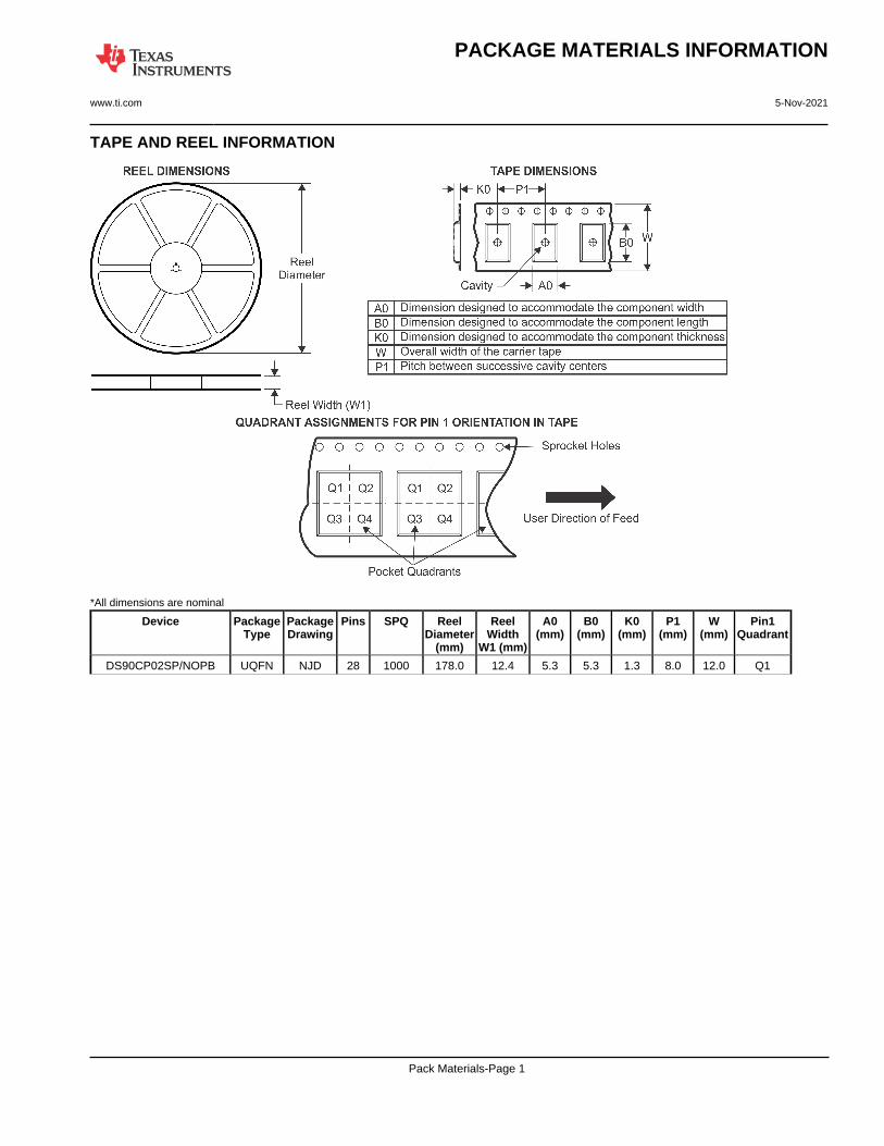
TAPE AND REEL INFORMATION
*All dimensions are nominal
Device PackageType
PackageDrawing
Pins SPQ ReelDiameter
(mm)
ReelWidth
W1 (mm)
A0(mm)
B0(mm)
K0(mm)
P1(mm)
W(mm)
Pin1Quadrant
DS90CP02SP/NOPB UQFN NJD 28 1000 178.0 12.4 5.3 5.3 1.3 8.0 12.0 Q1
PACKAGE MATERIALS INFORMATION
www.ti.com 5-Nov-2021
Pack Materials-Page 1
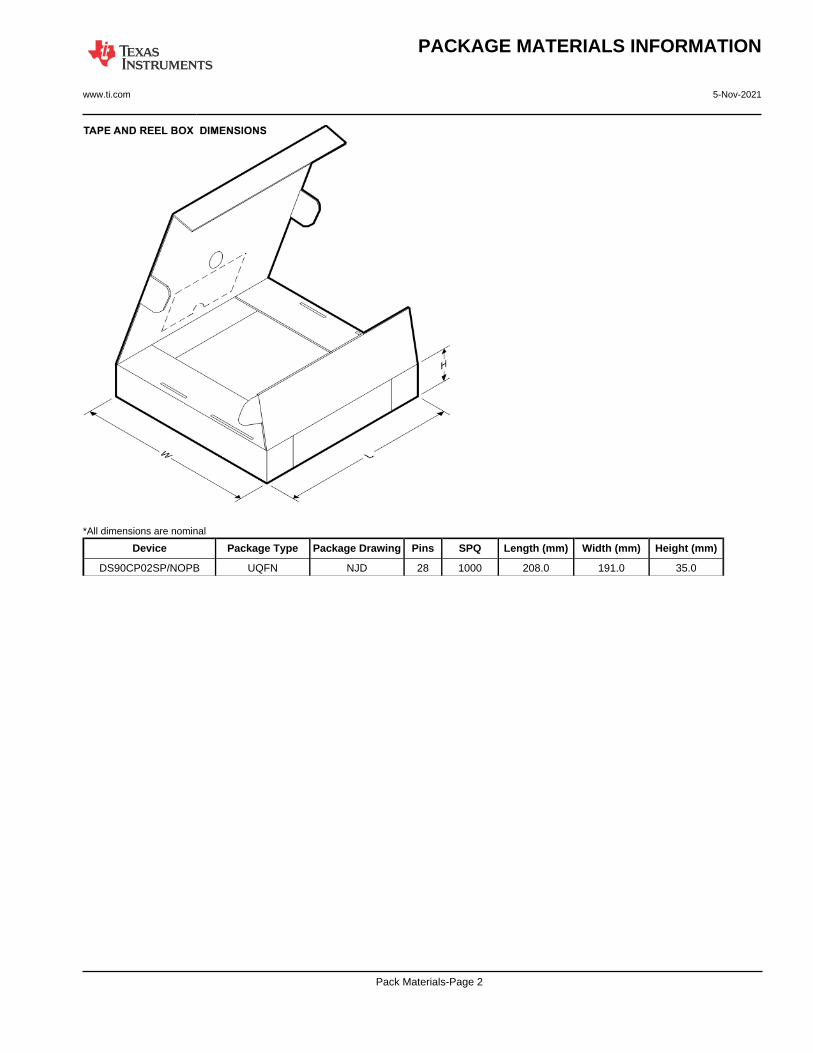
*All dimensions are nominal
Device Package Type Package Drawing Pins SPQ Length (mm) Width (mm) Height (mm)
DS90CP02SP/NOPB UQFN NJD 28 1000 208.0 191.0 35.0
PACKAGE MATERIALS INFORMATION
www.ti.com 5-Nov-2021
Pack Materials-Page 2
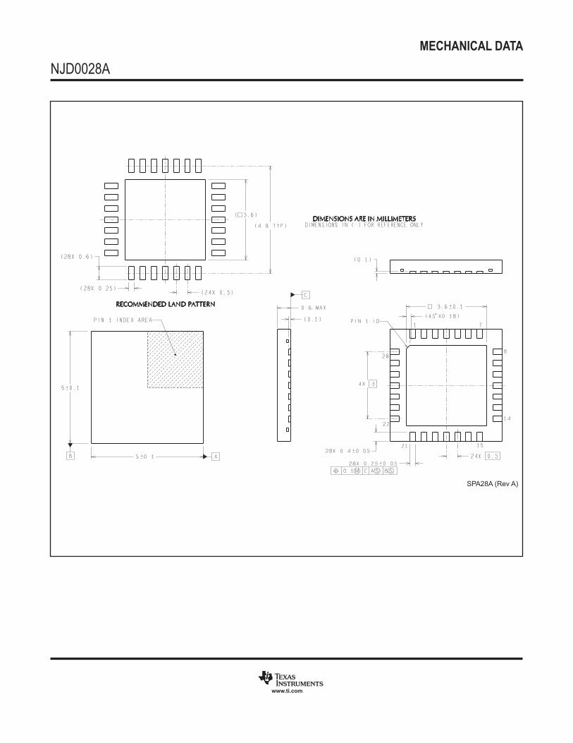
MECHANICAL DATA
NJD0028A
www.ti.com
SPA28A (Rev A)
IMPORTANT NOTICE AND DISCLAIMERTI PROVIDES TECHNICAL AND RELIABILITY DATA (INCLUDING DATA SHEETS), DESIGN RESOURCES (INCLUDING REFERENCE DESIGNS), APPLICATION OR OTHER DESIGN ADVICE, WEB TOOLS, SAFETY INFORMATION, AND OTHER RESOURCES “AS IS” AND WITH ALL FAULTS, AND DISCLAIMS ALL WARRANTIES, EXPRESS AND IMPLIED, INCLUDING WITHOUT LIMITATION ANY IMPLIED WARRANTIES OF MERCHANTABILITY, FITNESS FOR A PARTICULAR PURPOSE OR NON-INFRINGEMENT OF THIRD PARTY INTELLECTUAL PROPERTY RIGHTS.These resources are intended for skilled developers designing with TI products. You are solely responsible for (1) selecting the appropriate TI products for your application, (2) designing, validating and testing your application, and (3) ensuring your application meets applicable standards, and any other safety, security, regulatory or other requirements.These resources are subject to change without notice. TI grants you permission to use these resources only for development of an application that uses the TI products described in the resource. Other reproduction and display of these resources is prohibited. No license is granted to any other TI intellectual property right or to any third party intellectual property right. TI disclaims responsibility for, and you will fully indemnify TI and its representatives against, any claims, damages, costs, losses, and liabilities arising out of your use of these resources.TI’s products are provided subject to TI’s Terms of Sale or other applicable terms available either on ti.com or provided in conjunction with such TI products. TI’s provision of these resources does not expand or otherwise alter TI’s applicable warranties or warranty disclaimers for TI products.TI objects to and rejects any additional or different terms you may have proposed. IMPORTANT NOTICE
Mailing Address: Texas Instruments, Post Office Box 655303, Dallas, Texas 75265Copyright © 2021, Texas Instruments Incorporated