Embed Size (px)
Citation preview
2017 Microchip Technology Inc. DS50002632A
dsPIC33EP128GS808Development Board
User’s Guide
DS50002632A-page 2 2017 Microchip Technology Inc.
Information contained in this publication regarding deviceapplications and the like is provided only for your convenienceand may be superseded by updates. It is your responsibility toensure that your application meets with your specifications.MICROCHIP MAKES NO REPRESENTATIONS ORWARRANTIES OF ANY KIND WHETHER EXPRESS ORIMPLIED, WRITTEN OR ORAL, STATUTORY OROTHERWISE, RELATED TO THE INFORMATION,INCLUDING BUT NOT LIMITED TO ITS CONDITION,QUALITY, PERFORMANCE, MERCHANTABILITY ORFITNESS FOR PURPOSE. Microchip disclaims all liabilityarising from this information and its use. Use of Microchipdevices in life support and/or safety applications is entirely atthe buyer’s risk, and the buyer agrees to defend, indemnify andhold harmless Microchip from any and all damages, claims,suits, or expenses resulting from such use. No licenses areconveyed, implicitly or otherwise, under any Microchipintellectual property rights unless otherwise stated.
Note the following details of the code protection feature on Microchip devices:
• Microchip products meet the specification contained in their particular Microchip Data Sheet.
• Microchip believes that its family of products is one of the most secure families of its kind on the market today, when used in the intended manner and under normal conditions.
• There are dishonest and possibly illegal methods used to breach the code protection feature. All of these methods, to our knowledge, require using the Microchip products in a manner outside the operating specifications contained in Microchip’s Data Sheets. Most likely, the person doing so is engaged in theft of intellectual property.
• Microchip is willing to work with the customer who is concerned about the integrity of their code.
• Neither Microchip nor any other semiconductor manufacturer can guarantee the security of their code. Code protection does not mean that we are guaranteeing the product as “unbreakable.”
Code protection is constantly evolving. We at Microchip are committed to continuously improving the code protection features of ourproducts. Attempts to break Microchip’s code protection feature may be a violation of the Digital Millennium Copyright Act. If such actsallow unauthorized access to your software or other copyrighted work, you may have a right to sue for relief under that Act.
Microchip received ISO/TS-16949:2009 certification for its worldwide headquarters, design and wafer fabrication facilities in Chandler and Tempe, Arizona; Gresham, Oregon and design centers in California and India. The Company’s quality system processes and procedures are for its PIC® MCUs and dsPIC® DSCs, KEELOQ® code hopping devices, Serial EEPROMs, microperipherals, nonvolatile memory and analog products. In addition, Microchip’s quality system for the design and manufacture of development systems is ISO 9001:2000 certified.
QUALITY MANAGEMENT SYSTEM CERTIFIED BY DNV
== ISO/TS 16949 ==
Trademarks
The Microchip name and logo, the Microchip logo, AnyRate, AVR, AVR logo, AVR Freaks, BeaconThings, BitCloud, CryptoMemory, CryptoRF, dsPIC, FlashFlex, flexPWR, Heldo, JukeBlox, KEELOQ, KEELOQ logo, Kleer, LANCheck, LINK MD, maXStylus, maXTouch, MediaLB, megaAVR, MOST, MOST logo, MPLAB, OptoLyzer, PIC, picoPower, PICSTART, PIC32 logo, Prochip Designer, QTouch, RightTouch, SAM-BA, SpyNIC, SST, SST Logo, SuperFlash, tinyAVR, UNI/O, and XMEGA are registered trademarks of Microchip Technology Incorporated in the U.S.A. and other countries.
ClockWorks, The Embedded Control Solutions Company, EtherSynch, Hyper Speed Control, HyperLight Load, IntelliMOS, mTouch, Precision Edge, and Quiet-Wire are registered trademarks of Microchip Technology Incorporated in the U.S.A.
Adjacent Key Suppression, AKS, Analog-for-the-Digital Age, Any Capacitor, AnyIn, AnyOut, BodyCom, chipKIT, chipKIT logo, CodeGuard, CryptoAuthentication, CryptoCompanion, CryptoController, dsPICDEM, dsPICDEM.net, Dynamic Average Matching, DAM, ECAN, EtherGREEN, In-Circuit Serial Programming, ICSP, Inter-Chip Connectivity, JitterBlocker, KleerNet, KleerNet logo, Mindi, MiWi, motorBench, MPASM, MPF, MPLAB Certified logo, MPLIB, MPLINK, MultiTRAK, NetDetach, Omniscient Code Generation, PICDEM, PICDEM.net, PICkit, PICtail, PureSilicon, QMatrix, RightTouch logo, REAL ICE, Ripple Blocker, SAM-ICE, Serial Quad I/O, SMART-I.S., SQI, SuperSwitcher, SuperSwitcher II, Total Endurance, TSHARC, USBCheck, VariSense, ViewSpan, WiperLock, Wireless DNA, and ZENA are trademarks of Microchip Technology Incorporated in the U.S.A. and other countries.
SQTP is a service mark of Microchip Technology Incorporated in the U.S.A.
Silicon Storage Technology is a registered trademark of Microchip Technology Inc. in other countries.
GestIC is a registered trademark of Microchip Technology Germany II GmbH & Co. KG, a subsidiary of Microchip Technology Inc., in other countries.
All other trademarks mentioned herein are property of their respective companies.
© 2017, Microchip Technology Incorporated, All Rights Reserved.
ISBN: 978-1-5224-1406-3

EU Declaration of Conformity This declaration of conformity is issued by the manufacturer. The development/evaluation tool is designed to be used for research and development in a laboratory environment. This development/evaluation tool is not a Finished Appliance, nor is it intended for incorporation into Finished Appliances that are made commercially available as single functional units to end users under EU EMC Directive 2004/108/EC and as supported by the European Commission's Guide for the EMC Directive 2004/108/EC (8th February 2010). This development/evaluation tool complies with EU RoHS2 Directive 2011/65/EU. This development/evaluation tool, when incorporating wireless and radio-telecom functionality, is in compliance with the essential requirement and other relevant provisions of the R&TTE Directive 1999/5/EC and the FCC rules as stated in the declaration of conformity provided in the module datasheet and the module product page available at www.microchip.com. For information regarding the exclusive, limited warranties applicable to Microchip products, please see Microchip’s standard terms and conditions of sale, which are printed on our sales documentation and available at www.microchip.com. Signed for and on behalf of Microchip Technology Inc. at Chandler, Arizona, USA.
Object of Declaration: dsPIC33EP128GS808 Development Board
2017 Microchip Technology Inc. DS50002632A-page 3

dsPIC33EP128GS808 Development Board User’s Guide
NOTES:
DS50002632A-page 4 2017 Microchip Technology Inc.
dsPIC33EP128GS808 DEVELOPMENTBOARD USER’S GUIDE
Table of Contents
Preface ........................................................................................................................... 7Introduction............................................................................................................ 7
Document Layout .................................................................................................. 7
Conventions Used in this Guide ............................................................................ 8
Recommended Reading........................................................................................ 9
The Microchip Web Site ........................................................................................ 9
Product Change Notification Service..................................................................... 9
Customer Support ................................................................................................. 9
Document Revision History ................................................................................... 9
Chapter 1. Product Overview1.1 Introduction ................................................................................................... 111.2 Overview ...................................................................................................... 111.3 Development Board Functionality and Features .......................................... 121.4 Electrical Specifications ................................................................................ 12
Chapter 2. Hardware2.1 Top Assembly ............................................................................................... 132.2 Signal Configuration ..................................................................................... 152.3 Application Components .............................................................................. 172.4 Board Connectors ........................................................................................ 172.5 Indicators and Human Interfaces ................................................................. 182.6 Test Points ................................................................................................... 192.7 Programmer/Debugger ................................................................................. 20
Chapter 3. Demonstration Program Operation3.1 Hardware Description ................................................................................... 213.2 Program Demonstration ............................................................................... 253.3 Code Demonstration .................................................................................... 283.4 Other Code Examples .................................................................................. 30
Appendix A. Board Layout and Schematics.............................................................. 31
Worldwide Sales and Service .................................................................................... 36
2017 Microchip Technology Inc. DS50002632A-page 5
dsPIC33EP128GS808 Development Board User’s Guide
NOTES:
DS50002632A-page 6 <Conditional><7.arial> 2017 Microchip Technology Inc.
dsPIC33EP128GS808 DEVELOPMENT
BOARD USER’S GUIDEPreface
INTRODUCTIONThis chapter contains general information that will be useful to know before using the dsPIC33EP128GS808 Development Board. Items discussed in this chapter include:
• Document Layout
• Conventions Used in this Guide
• Recommended Reading
• The Microchip Web Site
• Customer Support
• Document Revision History
DOCUMENT LAYOUTThis document describes how to use the dsPIC33EP128GS808 Development Board as a development tool to emulate and debug firmware on a target board. The manual layout is as follows:
• Product Overview – This chapter introduces the dsPIC33EP128GS808 Development Board and provides an overview of its features.
• Hardware – This chapter describes the hardware components of the dsPIC33EP128GS808 Development Board.
• Demonstration Program Operation – This chapter includes a program demonstration, code demonstration and code examples for the dsPIC33EP128GS808 Development Board.
• Appendix A – Shows the schematics and board layouts for the dsPIC33EP128GS808 Development Board.
NOTICE TO CUSTOMERS
All documentation becomes dated, and this manual is no exception. Microchip tools and documentation are constantly evolving to meet customer needs, so some actual dialogs and/or tool descriptions may differ from those in this document. Please refer to our web site (www.microchip.com) to obtain the latest documentation available.
Documents are identified with a “DS” number. This number is located on the bottom of each page, in front of the page number. The numbering convention for the DS number is “DSXXXXXXXXA”, where “XXXXXXXX” is the document number and “A” is the revision level of the document.
For the most up-to-date information on development tools, see the MPLAB® IDE online help. Select the Help menu, and then Topics, to open a list of available online help files.
2017 Microchip Technology Inc. DS50002632A-page 7
dsPIC33EP128GS808 Development Board User’s Guide
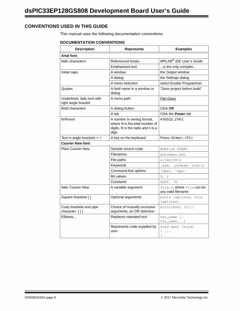
CONVENTIONS USED IN THIS GUIDE
This manual uses the following documentation conventions:
DOCUMENTATION CONVENTIONS
Description Represents Examples
Arial font:
Italic characters Referenced books MPLAB® IDE User’s Guide
Emphasized text ...is the only compiler...
Initial caps A window the Output window
A dialog the Settings dialog
A menu selection select Enable Programmer
Quotes A field name in a window or dialog
“Save project before build”
Underlined, italic text with right angle bracket
A menu path File>Save
Bold characters A dialog button Click OK
A tab Click the Power tab
N‘Rnnnn A number in verilog format, where N is the total number of digits, R is the radix and n is a digit.
4‘b0010, 2‘hF1
Text in angle brackets < > A key on the keyboard Press <Enter>, <F1>
Courier New font:
Plain Courier New Sample source code #define START
Filenames autoexec.bat
File paths c:\mcc18\h
Keywords _asm, _endasm, static
Command-line options -Opa+, -Opa-
Bit values 0, 1
Constants 0xFF, ‘A’
Italic Courier New A variable argument file.o, where file can be any valid filename
Square brackets [ ] Optional arguments mcc18 [options] file [options]
Curly brackets and pipe character: { | }
Choice of mutually exclusive arguments; an OR selection
errorlevel {0|1}
Ellipses... Replaces repeated text var_name [, var_name...]
Represents code supplied by user
void main (void){ ...}
DS50002632A-page 8 2017 Microchip Technology Inc.
Preface
RECOMMENDED READING
This quick start guide describes how to use the dsPIC33EP128GS808 Development Board. Other useful documents are listed below. The following Microchip document is available and recommended as a supplemental reference resource:
• “dsPIC33EPXXXGS70X/80X Family Data Sheet” (DS70005258)
THE MICROCHIP WEB SITE
Microchip provides online support via our web site at www.microchip.com. This web site is used as a means to make files and information easily available to customers. Accessible by using your favorite Internet browser, the web site contains the following information:
• Product Support – Data sheets and errata, application notes and sample programs, design resources, user’s guides and hardware support documents, latest software releases and archived software
• General Technical Support – Frequently Asked Questions (FAQs), technical support requests, online discussion groups, Microchip consultant program member listing
• Business of Microchip – Product selector and ordering guides, latest Microchip press releases, listing of seminars and events, listings of Microchip sales offices, distributors and factory representatives
PRODUCT CHANGE NOTIFICATION SERVICE
Microchip’s customer notification service helps keep customers current on Microchip products. Subscribers will receive e-mail notifications whenever there are changes, updates, revisions or errata related to a specified product family or development tool of interest.
To register, access the Microchip web site at www.microchip.com, click on Product Change Notification and follow the registration instructions.
CUSTOMER SUPPORT
Users of Microchip products can receive assistance through several channels:
• Distributor or Representative
• Local Sales Office
• Embedded Solutions Engineer (ESE)
• Technical Support
Customers should contact their distributor, representative or Embedded Solutions Engineer (ESE) for support. Local sales offices are also available to help customers. A listing of sales offices and locations is included in the back of this document.
Technical support is available through the web site at: http://www.microchip.com/support.
DOCUMENT REVISION HISTORY
Revision A (June 2017)
• Initial Release of this Document.
2017 Microchip Technology Inc. DS50002632A-page 9
dsPIC33EP128GS808 Development Board User’s Guide
NOTES:
DS50002632A-page 10 2017 Microchip Technology Inc.
dsPIC33EP128GS808 DEVELOPMENT
BOARD USER’S GUIDEChapter 1. Product Overview
1.1 INTRODUCTION
This chapter introduces the dsPIC33EP128GS808 Development Board and provides an overview of its features. The topics covered include:
• Overview
• Development Board Functionality and Features
• Electrical Specifications
1.2 OVERVIEW
The dsPIC33EP128GS808 Development Board (referred to as development board) is designed to aid in the evaluation and development of firmware for the dsPIC33EP ‘GS’ family of Digital Signal Controllers (DSCs). There are 3 primary objectives for development of this board:
• Evaluation of peripherals and core features of the GS family
• Support for dual CAN solutions with the “CAN/LIN/J2602 PICtail™ (Plus) Daughter Board User’s Guide” (DS70319)
• Demonstration of emulated power supply transient response
The development board can be used as a stand-alone platform for evaluating DSC core features, such as throughput and device peripherals, which include ADC, PWM, PGA, CMP, SPI, I2C, etc. Table 2-3 provides a comprehensive list of I/O signals available for evaluation. Note that the remappable I/Os provide additional flexibility to access additional signals on the I/O pins. Refer to the “dsPIC33EPXXXGS70X/80X Family Data Sheet” (DS70005258) for further details.
The development board provides support for development of dual CAN applications, along with the CAN/LIN/J2602 PICtail (Plus) Daughter Board. The CAN/LIN/J2602 PICtail (Plus) Daughter Board consists of 2 sets of CAN drivers and 2 sets of LIN drivers. The development board plugs into the PICtail board and allows development of CAN or LIN communication.
The development board contains multiple first-order RC filters to emulate power supply functionality. The board can be operated in Open or Closed-Loop mode. Furthermore, there is additional hardware on the board to simulate power supply transient behavior. The board can be powered with a standard 9V adapter or through the mini-USB. The board can be programmed with standard Microchip programming tools via an RJ25 connector and contains LEDs, switch, selectable jumpers for maximizing peripheral interconnectivity, potentiometers and analog feedback networks, all of which help to facilitate development of firmware on the dsPIC33EP ‘GS’ devices.
2017 Microchip Technology Inc. DS50002632A-page 11
dsPIC33EP128GS808 Development Board User’s Guide
1.3 DEVELOPMENT BOARD FUNCTIONALITY AND FEATURES
The dsPIC33EP128GS808 Development Board allows users to evaluate the features of dsPIC33EP ‘GS’ series devices. The dsPIC33EP ‘GS’ devices offer new peripherals and features that can be explored using the development board. Configurable connec-tors make it easy to connect different peripherals together to test features that would otherwise require additional hardware. The development board can also be used to develop dual CAN communication systems when used along with the CAN/LIN/J2602 PICtail (Plus) Daughter Board.
The development board provides the following features:
• Dual CAN/LIN Interface:
- Used as an add-on board to the CAN/LIN/J2602 PICtail (Plus) Daughter Board
- Interfaces with CAN and LIN drivers on the CAN/LIN/J2602 PICtail (Plus) Daughter Board
- Provides power to CAN and LIN drivers on the CAN/LIN/J2602 PICtail (Plus) Daughter Board
• Power Supply Simulation Using First-Order Filters:
- Separate voltage and current loop emulation
- Provision to simulate dynamic response
- Multiple first-order filters on board, selectable by jumpers
- Ramp generator circuit
- Constant-current test circuit
• General Features:
- External voltage input provision
- Debug switch and LEDs
- On-board power supply – operates from 9V input
- Optional USB power
- RJ25 connector programming interface
- PICkit™ 3 serial analyzer
1.4 ELECTRICAL SPECIFICATIONS
TABLE 1-1: DC INPUT RATING (J1)
Parameter Minimum Typical Maximum Units Remarks
Voltage 7.0 9 11 V 9V Adapter
Current 0.2 — — A Stand-Alone Mode
— — 0.7 A With CAN/LIN Operating on the PICtail™ Board
DS50002632A-page 12 2017 Microchip Technology Inc.
dsPIC33EP128GS808 DEVELOPMENT
BOARD USER’S GUIDEChapter 2. Hardware
This chapter describes the hardware components of the dsPIC33EP128GS808 Development Board. The topics covered include:
• Top Assembly
• Signal Configuration
• Application Components
• Board Connectors
• Indicators and Human Interfaces
• Test Points
• Programmer/Debugger
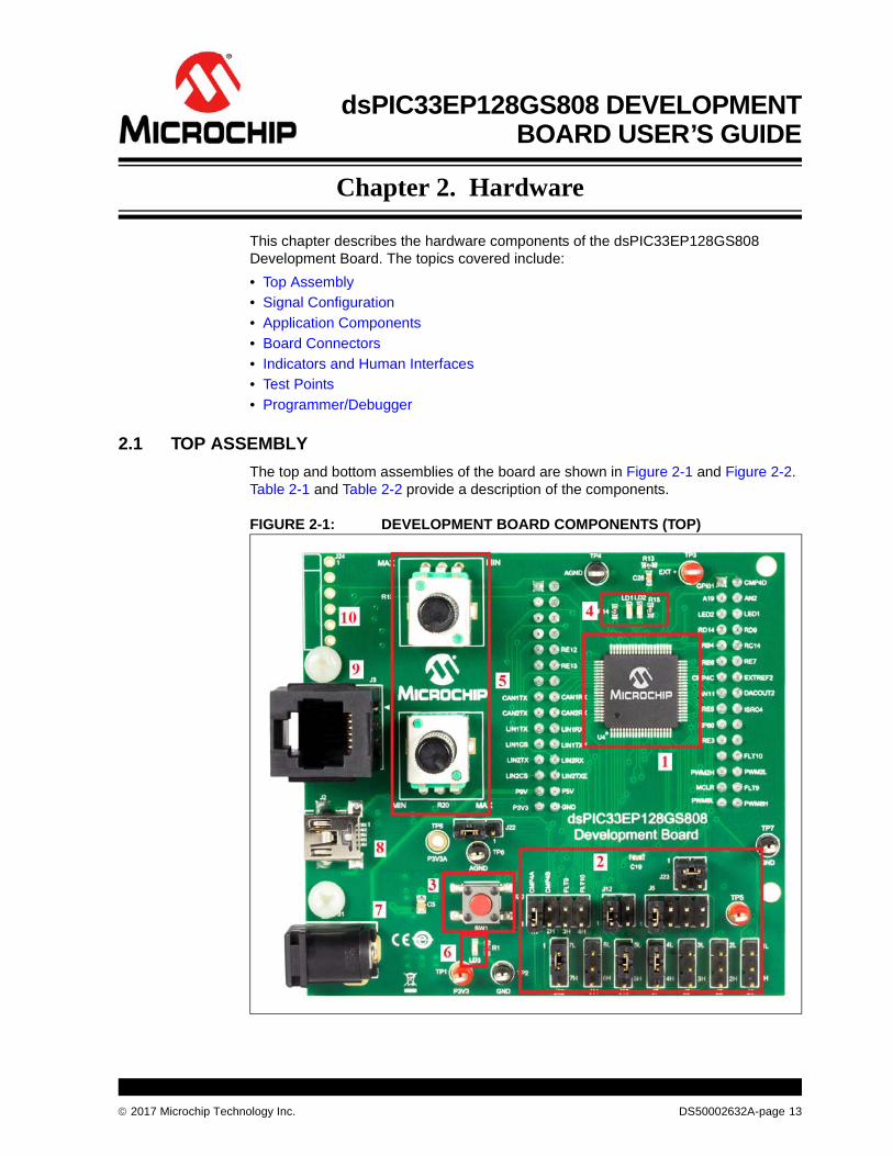
2.1 TOP ASSEMBLY
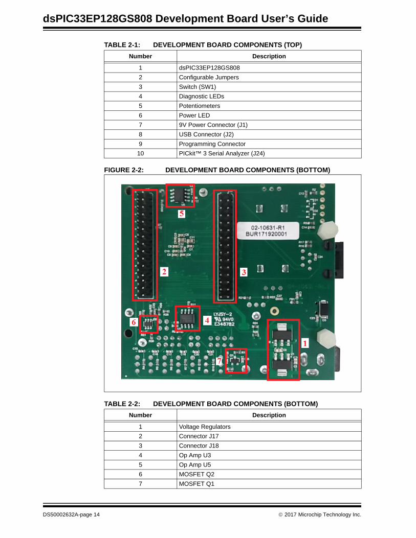
The top and bottom assemblies of the board are shown in Figure 2-1 and Figure 2-2. Table 2-1 and Table 2-2 provide a description of the components.
FIGURE 2-1: DEVELOPMENT BOARD COMPONENTS (TOP)
2017 Microchip Technology Inc. DS50002632A-page 13
dsPIC33EP128GS808 Development Board User’s Guide
TABLE 2-1: DEVELOPMENT BOARD COMPONENTS (TOP)
FIGURE 2-2: DEVELOPMENT BOARD COMPONENTS (BOTTOM)
TABLE 2-2: DEVELOPMENT BOARD COMPONENTS (BOTTOM)
Number Description
1 dsPIC33EP128GS808
2 Configurable Jumpers
3 Switch (SW1)
4 Diagnostic LEDs
5 Potentiometers
6 Power LED
7 9V Power Connector (J1)
8 USB Connector (J2)
9 Programming Connector
10 PICkit™ 3 Serial Analyzer (J24)
Number Description
1 Voltage Regulators
2 Connector J17
3 Connector J18
4 Op Amp U3
5 Op Amp U5
6 MOSFET Q2
7 MOSFET Q1
DS50002632A-page 14 2017 Microchip Technology Inc.
Hardware
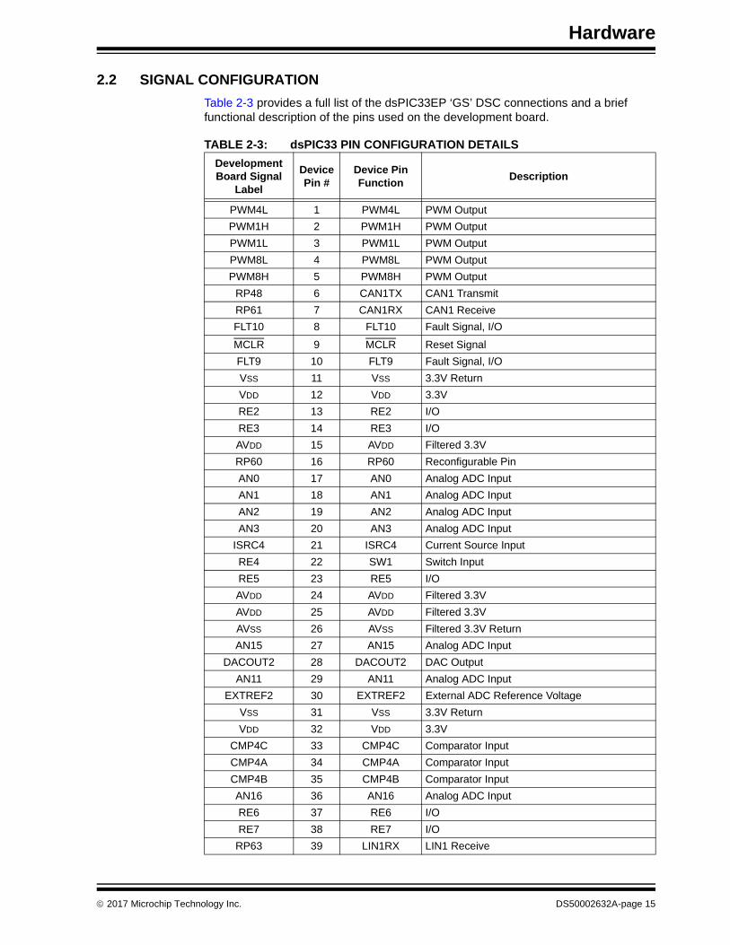
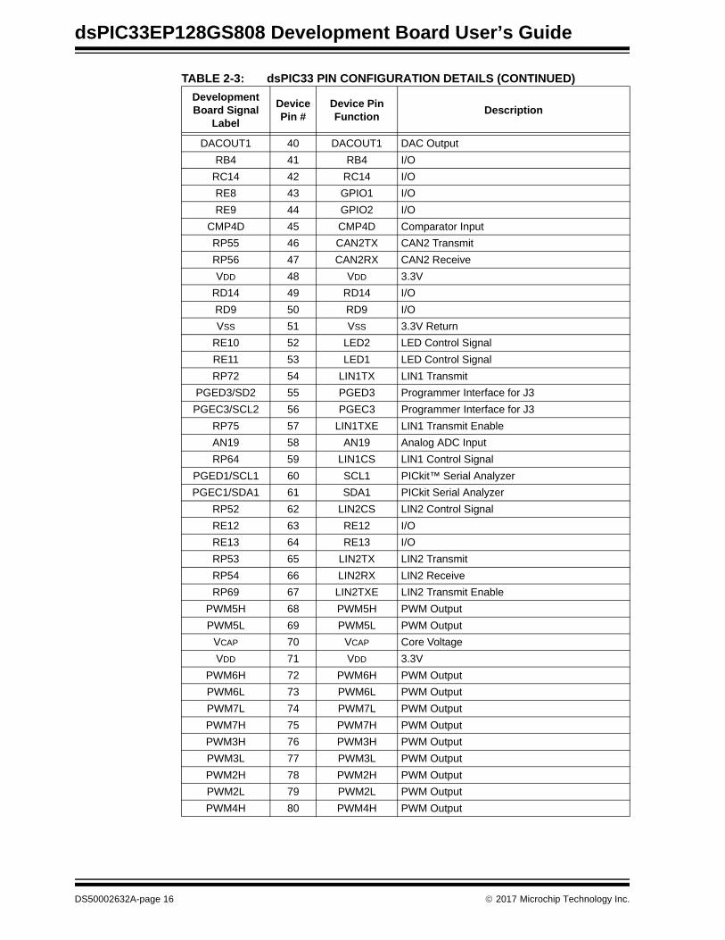
2.2 SIGNAL CONFIGURATION
Table 2-3 provides a full list of the dsPIC33EP ‘GS’ DSC connections and a brief functional description of the pins used on the development board.
TABLE 2-3: dsPIC33 PIN CONFIGURATION DETAILS
Development Board Signal
Label
DevicePin #
Device Pin Function
Description
PWM4L 1 PWM4L PWM Output
PWM1H 2 PWM1H PWM Output
PWM1L 3 PWM1L PWM Output
PWM8L 4 PWM8L PWM Output
PWM8H 5 PWM8H PWM Output
RP48 6 CAN1TX CAN1 Transmit
RP61 7 CAN1RX CAN1 Receive
FLT10 8 FLT10 Fault Signal, I/O
MCLR 9 MCLR Reset Signal
FLT9 10 FLT9 Fault Signal, I/O
VSS 11 VSS 3.3V Return
VDD 12 VDD 3.3V
RE2 13 RE2 I/O
RE3 14 RE3 I/O
AVDD 15 AVDD Filtered 3.3V
RP60 16 RP60 Reconfigurable Pin
AN0 17 AN0 Analog ADC Input
AN1 18 AN1 Analog ADC Input
AN2 19 AN2 Analog ADC Input
AN3 20 AN3 Analog ADC Input
ISRC4 21 ISRC4 Current Source Input
RE4 22 SW1 Switch Input
RE5 23 RE5 I/O
AVDD 24 AVDD Filtered 3.3V
AVDD 25 AVDD Filtered 3.3V
AVSS 26 AVSS Filtered 3.3V Return
AN15 27 AN15 Analog ADC Input
DACOUT2 28 DACOUT2 DAC Output
AN11 29 AN11 Analog ADC Input
EXTREF2 30 EXTREF2 External ADC Reference Voltage
VSS 31 VSS 3.3V Return
VDD 32 VDD 3.3V
CMP4C 33 CMP4C Comparator Input
CMP4A 34 CMP4A Comparator Input
CMP4B 35 CMP4B Comparator Input
AN16 36 AN16 Analog ADC Input
RE6 37 RE6 I/O
RE7 38 RE7 I/O
RP63 39 LIN1RX LIN1 Receive
2017 Microchip Technology Inc. DS50002632A-page 15
dsPIC33EP128GS808 Development Board User’s Guide
DACOUT1 40 DACOUT1 DAC Output
RB4 41 RB4 I/O
RC14 42 RC14 I/O
RE8 43 GPIO1 I/O
RE9 44 GPIO2 I/O
CMP4D 45 CMP4D Comparator Input
RP55 46 CAN2TX CAN2 Transmit
RP56 47 CAN2RX CAN2 Receive
VDD 48 VDD 3.3V
RD14 49 RD14 I/O
RD9 50 RD9 I/O
VSS 51 VSS 3.3V Return
RE10 52 LED2 LED Control Signal
RE11 53 LED1 LED Control Signal
RP72 54 LIN1TX LIN1 Transmit
PGED3/SD2 55 PGED3 Programmer Interface for J3
PGEC3/SCL2 56 PGEC3 Programmer Interface for J3
RP75 57 LIN1TXE LIN1 Transmit Enable
AN19 58 AN19 Analog ADC Input
RP64 59 LIN1CS LIN1 Control Signal
PGED1/SCL1 60 SCL1 PICkit™ Serial Analyzer
PGEC1/SDA1 61 SDA1 PICkit Serial Analyzer
RP52 62 LIN2CS LIN2 Control Signal
RE12 63 RE12 I/O
RE13 64 RE13 I/O
RP53 65 LIN2TX LIN2 Transmit
RP54 66 LIN2RX LIN2 Receive
RP69 67 LIN2TXE LIN2 Transmit Enable
PWM5H 68 PWM5H PWM Output
PWM5L 69 PWM5L PWM Output
VCAP 70 VCAP Core Voltage
VDD 71 VDD 3.3V
PWM6H 72 PWM6H PWM Output
PWM6L 73 PWM6L PWM Output
PWM7L 74 PWM7L PWM Output
PWM7H 75 PWM7H PWM Output
PWM3H 76 PWM3H PWM Output
PWM3L 77 PWM3L PWM Output
PWM2H 78 PWM2H PWM Output
PWM2L 79 PWM2L PWM Output
PWM4H 80 PWM4H PWM Output
TABLE 2-3: dsPIC33 PIN CONFIGURATION DETAILS (CONTINUED)
Development Board Signal
Label
DevicePin #
Device Pin Function
Description
DS50002632A-page 16 2017 Microchip Technology Inc.
Hardware
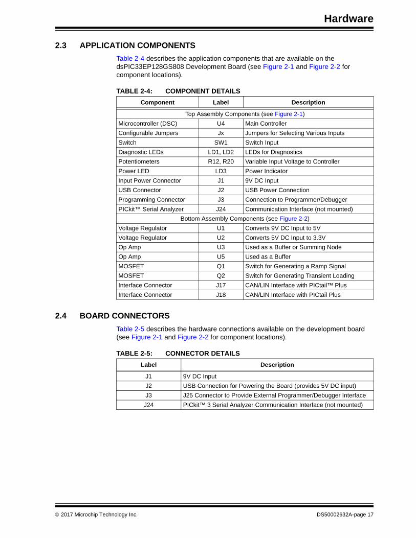
2.3 APPLICATION COMPONENTS
Table 2-4 describes the application components that are available on the dsPIC33EP128GS808 Development Board (see Figure 2-1 and Figure 2-2 for component locations).
TABLE 2-4: COMPONENT DETAILS
2.4 BOARD CONNECTORS
Table 2-5 describes the hardware connections available on the development board (see Figure 2-1 and Figure 2-2 for component locations).
TABLE 2-5: CONNECTOR DETAILS
Component Label Description
Top Assembly Components (see Figure 2-1)
Microcontroller (DSC) U4 Main Controller
Configurable Jumpers Jx Jumpers for Selecting Various Inputs
Switch SW1 Switch Input
Diagnostic LEDs LD1, LD2 LEDs for Diagnostics
Potentiometers R12, R20 Variable Input Voltage to Controller
Power LED LD3 Power Indicator
Input Power Connector J1 9V DC Input
USB Connector J2 USB Power Connection
Programming Connector J3 Connection to Programmer/Debugger
PICkit™ Serial Analyzer J24 Communication Interface (not mounted)
Bottom Assembly Components (see Figure 2-2)
Voltage Regulator U1 Converts 9V DC Input to 5V
Voltage Regulator U2 Converts 5V DC Input to 3.3V
Op Amp U3 Used as a Buffer or Summing Node
Op Amp U5 Used as a Buffer
MOSFET Q1 Switch for Generating a Ramp Signal
MOSFET Q2 Switch for Generating Transient Loading
Interface Connector J17 CAN/LIN Interface with PICtail™ Plus
Interface Connector J18 CAN/LIN Interface with PICtail Plus
Label Description
J1 9V DC Input
J2 USB Connection for Powering the Board (provides 5V DC input)
J3 J25 Connector to Provide External Programmer/Debugger Interface
J24 PICkit™ 3 Serial Analyzer Communication Interface (not mounted)
2017 Microchip Technology Inc. DS50002632A-page 17
dsPIC33EP128GS808 Development Board User’s Guide
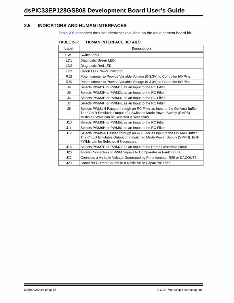
2.5 INDICATORS AND HUMAN INTERFACES
Table 2-6 describes the user interfaces available on the development board kit.
TABLE 2-6: HUMAN INTERFACE DETAILS
Label Description
SW1 Switch Input.
LD1 Diagnostic Green LED.
LD2 Diagnostic Red LED.
LD3 Green LED Power Indicator.
R12 Potentiometer to Provide Variable Voltage (0-3.3V) to Controller I/O Pins.
R20 Potentiometer to Provide Variable Voltage (0-3.3V) to Controller I/O Pins.
J4 Selects PWM1H or PWM1L as an Input to the RC Filter.
J5 Selects PWM2H or PWM2L as an Input to the RC Filter.
J6 Selects PWM3H or PWM3L as an Input to the RC Filter.
J7 Selects PWM4H or PWM4L as an Input to the RC Filter.
J8 Selects PWM1-4 Passed through an RC Filter as Input to the Op Amp Buffer. The Circuit Emulates Output of a Switched Mode Power Supply (SMPS). Multiple PWMs can be Selected if Necessary.
J10 Selects PWM5H or PWM5L as an Input to the RC Filter.
J11 Selects PWM6H or PWM6L as an Input to the RC Filter.
J12 Selects PWM5-6 Passed through an RC Filter as Input to the Op Amp Buffer. The Circuit Emulates Output of a Switched Mode Power Supply (SMPS). Both PWMs can be Selected if Necessary.
J15 Selects PWM7H or PWM7L as an Input to the Ramp Generator Circuit.
J20 Allows Connection of PWM Signals to Comparator or Fault Inputs.
J22 Connects a Variable Voltage Generated by Potentiometer R20 or DACOUT2.
J23 Connects Current Source to a Resistive or Capacitive Load.
DS50002632A-page 18 2017 Microchip Technology Inc.
Hardware
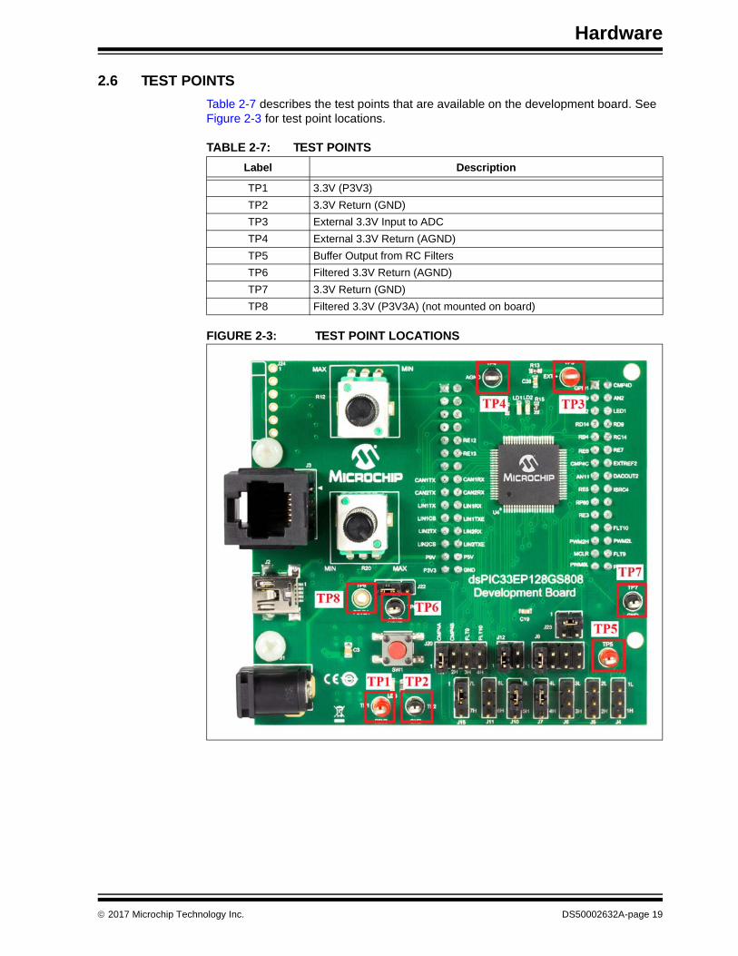
2.6 TEST POINTS
Table 2-7 describes the test points that are available on the development board. See Figure 2-3 for test point locations.
TABLE 2-7: TEST POINTS
FIGURE 2-3: TEST POINT LOCATIONS
Label Description
TP1 3.3V (P3V3)
TP2 3.3V Return (GND)
TP3 External 3.3V Input to ADC
TP4 External 3.3V Return (AGND)
TP5 Buffer Output from RC Filters
TP6 Filtered 3.3V Return (AGND)
TP7 3.3V Return (GND)
TP8 Filtered 3.3V (P3V3A) (not mounted on board)
2017 Microchip Technology Inc. DS50002632A-page 19
dsPIC33EP128GS808 Development Board User’s Guide
2.7 PROGRAMMER/DEBUGGER
The development board needs an external programmer/debugger, such as the MPLAB® ICD 3 or REAL ICE™ emulator to program the controller on the board.
TABLE 2-8: PROGRAMMER/DEBUGGER COMPONENTS
Component Label
Programmer/Debugger Connector
J3 RJ25 Connection for Interface to MPLAB® ICD 3 (DV164035)/REAL ICE™ Emulator (DV244005)
DS50002632A-page 20 2017 Microchip Technology Inc.
dsPIC33EP128GS808 DEVELOPMENT
BOARD USER’S GUIDEChapter 3. Demonstration Program Operation
The dsPIC33EP128GS808 Development Board is preprogrammed with application software that emulates the closed-loop operation of a power supply. The program illus-trates 2-Pole, 2-Zero (2P2Z) compensator control of the output voltage for the power supply emulation circuit. This code can be downloaded from Microchip web site (www.microchip.com).
This section covers the following topics:
• Hardware Description
• Software Demonstration
• Code Demonstration
• Other Code Examples
3.1 HARDWARE DESCRIPTION
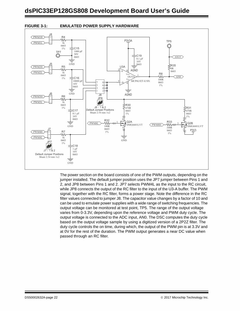
The hardware on the development board emulates the behavior of a power supply. Most of the power supply topologies consist of 2nd order Inductor-Capacitor (LC) filters, which smooth out the high-frequency switching content from the output voltage, resulting in a DC output voltage. The controller monitors the output voltage, compares it with a reference voltage and generates the required PWM duty cycle to maintain the output voltage equal to the reference voltage. The switching frequency is fixed and the output voltage regulation is maintained by controlling the on time of the switch. The ratio of the on time to the total switch duration is known as the duty cycle. The DSC implements a digital compensator, with the voltage error as input and the duty cycle as output. The development board does not use any inductor, but relies on the single-order RC filter and PWM to emulate the power stage of the supply. Figure 3-1 shows the hardware used for emulating the power supply.
2017 Microchip Technology Inc. DS50002632A-page 21
dsPIC33EP128GS808 Development Board User’s Guide
FIGURE 3-1: EMULATED POWER SUPPLY HARDWARE
The power section on the board consists of one of the PWM outputs, depending on the jumper installed. The default jumper position uses the JP7 jumper between Pins 1 and 2, and JP8 between Pins 1 and 2. JP7 selects PWM4L as the input to the RC circuit, while JP8 connects the output of the RC filter to the input of the U3-A buffer. The PWM signal, together with the RC filter, forms a power stage. Note the difference in the RC filter values connected to jumper J8. The capacitor value changes by a factor of 10 and can be used to emulate power supplies with a wide range of switching frequencies. The output voltage can be monitored at test point, TP5. The range of the output voltage varies from 0-3.3V, depending upon the reference voltage and PWM duty cycle. The output voltage is connected to the ADC input, AN0. The DSC computes the duty cycle based on the output voltage sample by using a digitized version of a 2P2Z filter. The duty cycle controls the on time, during which, the output of the PWM pin is at 3.3V and at 0V for the rest of the duration. The PWM output generates a near DC value when passed through an RC filter.
+A3
-A2
OUTA 1
+A
-A
OUTA
A
AVSS
4
VDD
8
MCP6L92T-E/SN
U3A
12
3
J4
12
3
J5
12
3
J6
12
3
J7
1k06031%
R4
1k06031%
R5
1k06031%
R6
1k06031%
R7
1 µF16V0603
C18
10000 pF16V0603
C16
1000 pF50V0603
C15
0.1 µF16V0603
C17
11 23 45 67 8
J8
GND
GND
GND
GND
PWM1H
PWM1L
PWM2H
PWM2L
PWM3H
PWM3L
PWM4H
PWM4L
P3V3A
0.1 µF16V0603
C19
AGND
AGND
100R06031%
R8
AN15
AN0
G2 3
D24
S22
DMG6601LVTQ2BG1 1
S15
D16
DMG6601LVTQ2A
470R06031%
R31470R06031%
R30
GND
P3V3100R06031%
R32
100R06031%
R33PWM8L PWM8H
0R0603
R35
TP5
TP7
Shunt 2.54 mm 1x2
JP7
Shunt 2.54 mm 1x2
JP8
Default Jumper PositionsJ7 – 1 & 2
Default Jumper PositionsJ8 – 1 & 2
DS50002632A-page 22 2017 Microchip Technology Inc.
Demonstration Program Operation
The load current in a power supply is dependent on the external load impedance and could be constant or varying. The real test for a power supply is when the load transitions from 0% to 100% or from 100% to 0% of rated current values. In a non-regulated power supply, a load transition leads to a drastic fall/rise in the output voltage. However, in a well regulated closed-loop system, a load transient will lead to a smaller output voltage drop (rise) when transitioning from 0 to 100% (100 to 0%), depending on the control design. The development board has additional hardware provided by the Q2 MOSFET to emulate the power supply loading condition. The Q2A and Q2B MOSFETS are controlled by signals PWM8L and PWM8H respectively. Q2A is connected between the buffer input and GND, while Q2B is connected between the buffer input and 3.3V. When Q2A is turned on, the buffer input gets pulled down to GND through the R30 resistor. Depending on the duration of the PWM8L pulse, the output voltage is pulled down from its steady-state value, thereby emulating a 0 to100% loading condition. Figures 3-2 and 3-3 indicate the transient loading condition. The green waveform corresponds to the PWM4L signal and the blue waveform to the buffer output (TP5) in the following figures.
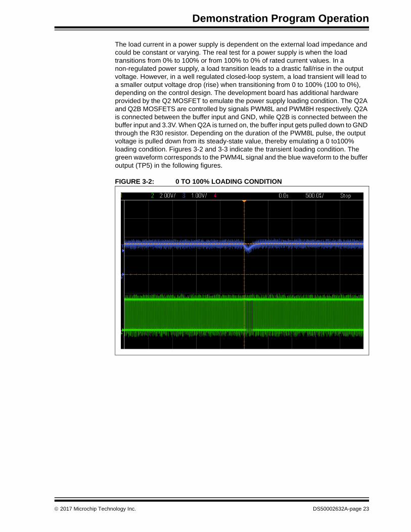
FIGURE 3-2: 0 TO 100% LOADING CONDITION
2017 Microchip Technology Inc. DS50002632A-page 23
dsPIC33EP128GS808 Development Board User’s Guide
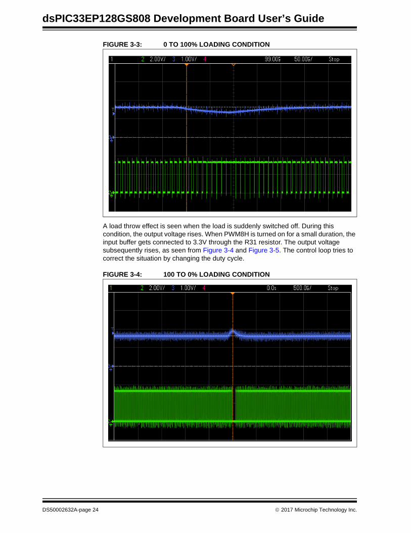
FIGURE 3-3: 0 TO 100% LOADING CONDITION
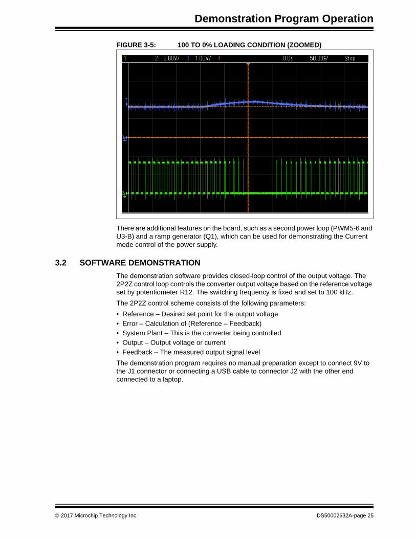
A load throw effect is seen when the load is suddenly switched off. During this condition, the output voltage rises. When PWM8H is turned on for a small duration, the input buffer gets connected to 3.3V through the R31 resistor. The output voltage subsequently rises, as seen from Figure 3-4 and Figure 3-5. The control loop tries to correct the situation by changing the duty cycle.
FIGURE 3-4: 100 TO 0% LOADING CONDITION
DS50002632A-page 24 2017 Microchip Technology Inc.
Demonstration Program Operation
FIGURE 3-5: 100 TO 0% LOADING CONDITION (ZOOMED)
There are additional features on the board, such as a second power loop (PWM5-6 and U3-B) and a ramp generator (Q1), which can be used for demonstrating the Current mode control of the power supply.
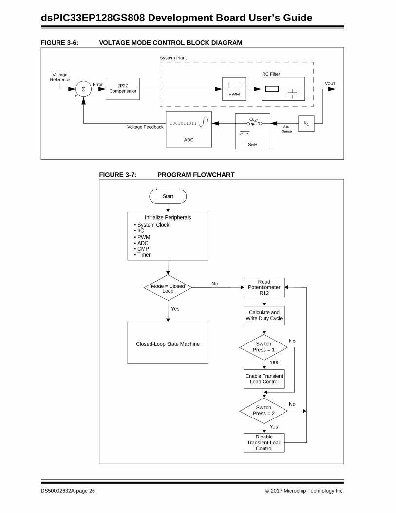
3.2 SOFTWARE DEMONSTRATION
The demonstration software provides closed-loop control of the output voltage. The 2P2Z control loop controls the converter output voltage based on the reference voltage set by potentiometer R12. The switching frequency is fixed and set to 100 kHz.
The 2P2Z control scheme consists of the following parameters:
• Reference – Desired set point for the output voltage
• Error – Calculation of (Reference – Feedback)
• System Plant – This is the converter being controlled
• Output – Output voltage or current
• Feedback – The measured output signal level
The demonstration program requires no manual preparation except to connect 9V to the J1 connector or connecting a USB cable to connector J2 with the other end connected to a laptop.
2017 Microchip Technology Inc. DS50002632A-page 25
dsPIC33EP128GS808 Development Board User’s Guide
FIGURE 3-6: VOLTAGE MODE CONTROL BLOCK DIAGRAM
FIGURE 3-7: PROGRAM FLOWCHART
VoltageReference
Error
+ –
2P2Z
Compensator
System Plant
PWM
RC Filter
VOUT
Voltage Feedback1001011011
ADCS&H
K1VOUT
Sense
Start
Initialize Peripherals
• I/O• PWM• ADC• CMP• Timer
Mode = ClosedLoop
Closed-Loop State Machine
Read
Calculate andWrite Duty Cycle
SwitchPress = 1
Enable TransientLoad Control
SwitchPress = 2
DisableTransient Load
Control
Yes
Yes
No
Yes
• System Clock
PotentiometerR12
No
No
DS50002632A-page 26 2017 Microchip Technology Inc.
Demonstration Program Operation
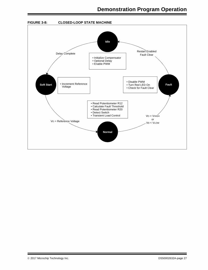
FIGURE 3-8: CLOSED-LOOP STATE MACHINE
• Initialize Compensator• Optional Delay• Enable PWM
• Increment ReferenceVoltage
• Read Potentiometer R12• Calculate Fault Threshold• Read Potentiometer R20• Detect Switch• Transient Load Control
• Disable PWM• Turn Red LED On• Check for Fault Clear
Restart EnabledFault Clear
VO > VHIGH
orVo < VLOW
VO = Reference Voltage
Delay Complete
Fault
Idle
Soft Start
Normal
2017 Microchip Technology Inc. DS50002632A-page 27
dsPIC33EP128GS808 Development Board User’s Guide
3.3 CODE DEMONSTRATION
The software code is based on a state machine, implemented as a foreground process, and interrupt routines are executed in the background. After the initialization phase, the code checks for the operating mode. If it is Open-Loop mode, the output voltage is set to the value decided by potentiometer R12. If it is Closed Loop mode, the state machine routine is executed. There are four states in the state machine, namely Idle, Soft Start, Normal and Fault. The details of each mode are given in the following sections.
3.3.1 System Initialization
When power is applied to the board, the program starts by executing the following system initialization routines:
• Peripherals – The required peripherals (PWM, ADC, Comparators, Timers and GPIO) are configured and enabled.
• Interrupts – Include ADC(s), Timer(s) and comparator(s) interrupts.
3.3.2 Modes
There are two modes of operation: Open-Loop mode and Closed-Loop mode. The Closed-Loop mode is set as the default. In the Open-Loop mode, the output of the PWM is set based on the value set by potentiometer R12. The Open-Loop mode does not execute any Soft Start or Fault state, but executes a load control routine. The tran-sient response of the supply can be monitored by pressing the SW1 switch once. This enables the load control routine, where the transient pulses appear periodically.
In the Closed-Loop mode, the output voltage is set by the control loop based on the reference voltage set. The Closed-Loop mode executes Idle, Soft Start, Normal and Fault states, as shown in Figure 3-8. Load control is part of the Normal state. During load control, if SW1 is pressed once, a transient pulse of duration LDTRANSTIME is applied to MOSFET Q2 with a repeat duration of LDPERIOD. The default settings are set to 1000 µs (LDTRANSTIME) and 1000 ms (LDPERIOD). Depending on the LOADSW setting to PULLUP or PULLDOWN in the user.h file, MOSFET Q2A or Q2B is controlled. A second press of SW1 will turn off the load control feature.
The mode can be changed by setting the variable, MODE, to either OPENLOOPDEMO or CLOSELOOPDEMO in the user.h file.
3.3.2.1 IDLE STATE
During the Idle state, the 2P2Z compensator is initialized. The ADC reads the value of potentiometer R12 and sets the reference voltage of the output. The PWM module and the interrupts are enabled in this state. Once all the tasks are completed, the next state is set to Soft Start.
3.3.2.2 SOFT START STATE
In this state, the Soft Start routine ramps up the output voltage in a closed-loop fashion until it is at the programmed output voltage value. This routine ensures that the output does not overshoot the desired voltage caused by a sudden inrush of current.
DS50002632A-page 28 2017 Microchip Technology Inc.
Demonstration Program Operation
3.3.2.3 NORMAL STATE
The program reaches the Normal state of operation after Soft Start is complete and stays in this state as long as the operating parameters are within the Fault threshold. The routine checks for a switch press to enable/disable transient pulses. The Fault thresholds are set based on the value of the output voltage. Alternately, the Fault thresholds can be set by potentiometer R20. This helps in changing the thresholds to verify the Fault condition. The ADC interrupt routine runs in the background and occurs at regular intervals of the PWM cycle (decided by the TRIG value). The ADC routine samples the output voltage and runs the 2P2Z controller.
The 2-Pole, 2-Zero (2P2Z) controller, implemented in software, is the digital implemen-tation of the Analog Type II controller. This filter maintains regulation of the output voltage and ensures stability during different line/load conditions. This controller requires three feedback errors multiplied by their associated coefficients, plus the two latest controller output values multiplied by their associated coefficients, along the delay line to provide proper compensation of the power converter. The control design is carried out using the DCDT tool which can be installed as an MPLAB® X plug-in. The DCDT supports different types of filters, such as 2P2Z, 3P3Z, PID, etc. The bode plots of the system plant, compensator and overall system can be viewed with the DCDT tool. The tool automatically converts the design into digital form and generates the coefficients. The coefficient file, filterx_dcdt.h, is added as a header file to the project. The filter routine is written in assembly language for faster execution. The routine, smps_2p2z_dspic_v2.s, refers to the coefficient file and creates a duty cycle based on the output voltage error.
During operation in Normal mode, the output voltage is checked against Fault thresh-olds. The Fault checking occurs at a fixed interval, set by Timer2, in the timer interrupt routine. The Fault is enabled or disabled based on the value set for VLTFLTENABLED in the user.h file. If the output voltage is beyond the thresholds, the state machine changes state to Fault mode.
3.3.2.4 FAULT STATE
The program enters the Fault mode when the output voltage is beyond the Fault thresholds. The PWM module is disabled immediately after entering the Fault state routine. The red LED is lit continuously for visual indication of a Fault. Based on the value set for RESTARTENABLED in the user.h file, the program enters Latch mode or Restart mode. In Latch mode, the program enters an endless while loop and needs a power recycle to start again. In the Restart mode, the routine checks for Faults to clear and enters Idle mode to start all over again.
2017 Microchip Technology Inc. DS50002632A-page 29
dsPIC33EP128GS808 Development Board User’s Guide
3.4 OTHER CODE EXAMPLES
There are several code examples available on the Microchip web site. One such code example developed exclusively for this board is mentioned below. Refer to the Readme files located in each code example folder for details on what each code example demonstrates. Check the Microchip web site (www.microchip.com/SMPS) for the latest updates to the code examples and for additional code examples.
3.4.1 Dual CAN Communication
The dual CAN communication code is provided to demonstrate basic control of LEDs on the development board. The development board is connected to the CAN/LIN/J2602 PICtail™ (Plus) Daughter Board, which is connected to the CAN host (CAN analyzer). The CAN host communicates with both the CAN (CAN1/CAN2) modules on the development board. Each CAN module has a specific address. The controller on the development board reads the potentiometers R12 and R20, and sends the value to the CAN host periodically, along with the CAN module address. The CAN host sends specific timer values for the CAN1 and CAN2 modules, which are used to blink the LEDs. Thus, changing the potentiometer on the development board will change the LED blink rate based on successful CAN communication.
3.4.2 Other Code Ideas
The development board is versatile and can be programmed to test a number of features. Most of the I/O pins are accessible on one of the several connectors on the board. The connector pins can be used to monitor outputs, connect input signals or provide cross connection between different controller pins. Some of the code ideas are:
• Peak Current Mode Control
• Ramp Generation
• ADC Reference Voltage Control
• Constant Current Source
• Peripheral Pin Select (PPS)
• I2C Communication
• PGA
• PTG/CLC
• PWM Signal as a Fault/Comparator Input
• Fault/Current Limit
• External Period Reset
DS50002632A-page 30 2017 Microchip Technology Inc.
dsPIC33EP128GS808 DEVELOPMENT
BOARD USER’S GUIDEAppendix A. Board Layout and Schematics
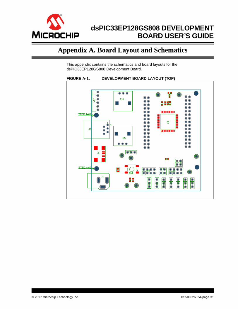
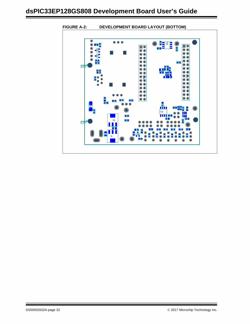
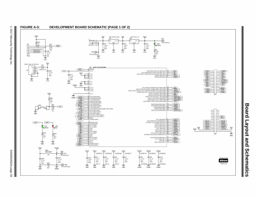
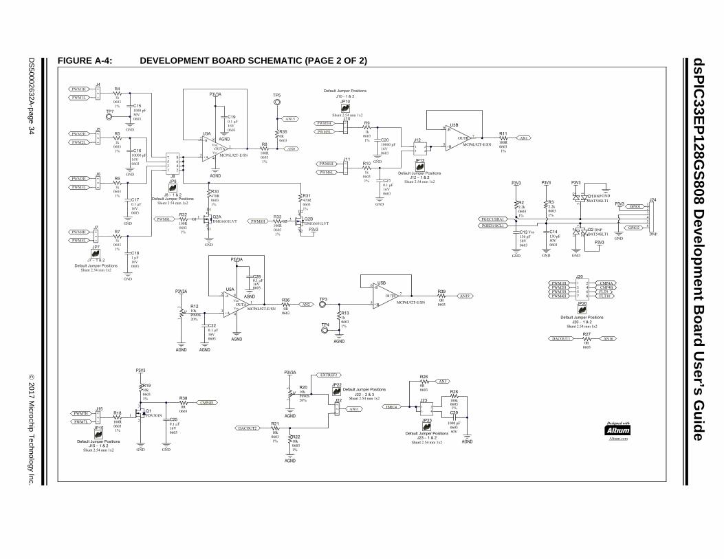
This appendix contains the schematics and board layouts for the dsPIC33EP128GS808 Development Board.
FIGURE A-1: DEVELOPMENT BOARD LAYOUT (TOP)
2017 Microchip Technology Inc. DS50002632A-page 31
dsPIC33EP128GS808 Development Board User’s Guide
FIGURE A-2: DEVELOPMENT BOARD LAYOUT (BOTTOM)
DS50002632A-page 32 2017 Microchip Technology Inc.
Bo
ard L
ayou
t and
Sch
ematics
2
01
7 M
icroch
ip T
ech
no
log
y Inc.
DS
50
00
26
32
A-p
ag
e 3
3
FIG
Designed with
Altium.com
1 23 4
5 67 8
9 1011 12
13 1415 16
17 1819 20
222123 24
25 2627 28
29 30
J17
1 23 4
5 67 8
9 1011 12
13 1415 16
17 1819 20
222123 24
25 2627 28
29 30
J18
CAN2TX CAN2RXLIN1TX LIN1RX
LIN1TXELIN2RX
LIN2CS LIN2TXEP3V3
CAN1TX CAN1RX
LIN1CSLIN2TX
GND
P5VP9V
GPIO1 CMP4DAN19 AN2LED2 LED1RD14 RD9
RB4 RC14RE6 RE7
CMP4C EXTREF2AN11 DACOUT2
RE5 ISRC4
FLT10PWM2H
MCLR FLT9PWM2L
PWM8L PWM8H
RE12RE13
RE2RE3
RP60
URE A-3: DEVELOPMENT BOARD SCHEMATIC (PAGE 1 OF 2)
231
POWER 2.1 mm
J1
GND2
VIN1 VOUT
3
MCP1703/3.3VU2
P9V P5V
10 µF16V0805
C110 µF16V0805
C210 µF16V0805
C3GND2
VIN1 VOUT
3
MIC39100-5.0WSU1
GND GND GND
GND
TP LOOP Red
TP1
330R06031%
R1
GND
TP LOOP Black
TP2 GND GND
P3V3
PWM4L
PWM1HPWM1L
PWM8LPWM8H
CAN1TX
CAN1RX
FLT10
MCLR
FLT9
GND
P3V3
0.1 µF16V0603
C4
GND
RE2RE3
P3V3U4 PIN 12
Pin 11
0.1 µF16V0603
C5
GND
P3V3U4 PIN 32
Pin 31
0.1 µF16V0603
C6
GND
P3V3U4 PIN 48
Pin 51
0.1 µF16V0603
C7
GND
P3V3U4 PIN 71
P3V3A
0.1 µF16V0603
C8
AGND
P3V3A
P3V3A
0.1 µF16V0603
C9
AGND
P3V3A
0.1 µF16V0603
C10
AGND
AGND
U4 PIN 15 U4 PIN 24 U4 PIN 25
U4 PIN 26 U4 PIN 26 U4 PIN 26
RP60
AN0AN1AN2
AN3
ISRC4
SW1
AN15
DACOUT2
AN11EXTREF2
CMP4C
CMP4ACMP4B
AN16
DACOUT1
GPIO1GPIO2
CMP4D
CAN2TXCAN2RX
LIN1TX
LIN1RX
LIN1CS
LIN1TXE
AN19PGED1/SCL1PGEC1/SDA1
LIN2TXLIN2RX
LIN2CS
LIN2TXEPWM5H
PWM5L
10 µF25V0805
C11
GND
VCAP
PWM6H
PWM6L
PWM7HPWM7L
PWM3HPWM3LPWM2HPWM2L
PWM4H
10 µF25V0805
C12
P3V3
GND
dsPIC33EP128GS808
PWM4L/RP67/RD31
PWM1H/RP20/RA4 2PWM1L/RP19/RA3 3
PWM8L/RE04
PWM8H/RE15
FLT12/RP48/RC0 6
FLT11/RP61/RC13 7
FLT10/RP74/RD108
MCLR9
T5CK/FLT9/RP76/RD1210
VSS11
VDD12
FLT17/RE213
FLT18/RE314
AVDD15
AN14/PGA2N3/RP60/RC12 16
AN0/CMP1A/PGA1P1/RP16/RA0 17
AN1/CMP1B/PGA1P2/PGA2P1/RP17/RA1 18
AN2/CMP1C/CMP2A/PGA1P3/PGA2P2/RP18/RA2 19
AN3/CMP1D/CMP2B/PGA2P3/RP32/RB0 20
AN4/CMP2C/CMP3A/ISRC4/RP41/RB9 21
RE422
RE523
AVDD24
AVDD25
AVSS26
AN15/RP71/RD727
DACOUT2/AN13/RD1328
AN11/PGA1N3/RP57/RC9 29
EXTREF2/AN10/PGA1P4/RP58/RC10 30
VSS31
VDD32
AN8/CMP4C/PGA2P4/RP49/RC1 33
OSCI/CLKI/AN6/CMP3C/CMP4A/ISRC2/RP33/RB1 34
OSC2/CLKO/AN0ALT/AN7/CMP3D/CMP4B/PGA1N2/RP34/RB2 35
AN16/RP66/RD236
FLT19/RE637
FLT20/RE738
RP63/ASDA2/RC15 39
PGED2/DACOUT1/AN18/ASCL2/INT0/RP35/RB3 40
PGEC2/ADTRG31/RP36/RB4 41
RP62/RC14 42
RE843
RE944
EXTREF1/AN9/CMP4D/RP50/RC2 45
RP55/ASDA1/RC7 46
RP56/ASCL1/RC8 47
VDD48
RD1449
SCK3/RP73/RD950
VSS51
FLT21/RE1052
FLT22/RE1153
AN5/CMP2D/CMP3B/ISRC3/RP72/RD854
PGED3/SDA2/FLT31/RP40/RB8 55
PGEC3/SCL2/RP47/RB15 56
INT4/RP75/RD1157
TD0/AN19/PGA2N2/RP37/RB5 58
T4CK/RP64/RD059 PGED1/TDI/AN20/SCL1/RP38/RB6 60
PGEC1/AN21/SDA1/RP39/RB7 61
AN1ALT/RP52/RC4 62
RE1263
RE1364
AN0ALT/RP53/RC5 65
AN17/RP54/RC6 66
AN12/RP69/RD567
PWM5H/RP70/RD668
PWM5L/RP51/RC3 69
VCAP70
VDD71
PWM6H/RP68/RD472
PWM6L/RD1573
PWM7L/RE1474
PWM7H/RE1575
TMS/PWM3H/RP43/RB11 76
TCK/PWM3L/RP44/RB12 77
PWM2H/RP45/RB13 78
PWM2L/RP46/RB14 79
PWM4H/RP65/RD180
U4
LED1
1k06031%
R141k06031%
R15
GND GND
LED2
RJ 25
12
34
56
J3 10k06031%
R16
470R06031%
R17
P3V3
MCLR
0.1 µF16V0603
C24PGED3/SDA2PGEC3/SCL2
GND
ID 4
VBUS1
GND 5
D- 2
D+ 3
0
USB2.0 Mini-B FEMALE
J2
GND
0.1 µF16V0603
C23
GND
26R
FB1
0.1 µF16V0603
C26 0.1 µF16V0603
C27
0R0603
R23
GND AGNDTP LOOP Black
TP6
1 4
2 3
SW1
GND
470R06031%
R24
10k06031%
R25
P3V3
SW1
CDBA120-G
D3
P3V3
P5V
P3V3A
RB4
RC14
TP LOOP RedDNP
TP8
PGED3/SDA2
PGEC3/SCL2
LED2LED1
RD14
RD9
RE6RE7
RE5
RE12RE13
GREENLD1
GREENLD3
REDLD2
dsP
IC33E
P128G
S8
08 Develo
pm
ent B
oard
User’s G
uid
e
DS
50
00
26
32
A-p
ag
e 3
4
20
17
Micro
chip
Te
chn
olo
gy In
c.
Designed with
Altium.com
123
BAT54SLT1DNPD1
1 23
BAT54SLT1DNPD2
130 pF50V0603
YesC13130 pF50V0603
C14
2.2k06031%
R22.2k06031%
R3
100R06031%
R11AN1
0R0603
R27DACOUT1 AN16
11 23 45 67 8
J20PWM1HPWM2HPWM3HPWM4H
CMP4ACMP4BFLT9FLT10
DNP
123456
J24
P3V3 P3V3
GND GND
P3V3
P3V3
GND
GND
P3V3 GPIO1
GPIO2
GND
SDA1
/SCL1
Shunt 2.54 mm 1x2
JP20
Default Jumper PositionsJ20 – 1 & 2
FIGURE A-4: DEVELOPMENT BOARD SCHEMATIC (PAGE 2 OF 2)
+A3
-A2
OUTA 1
+A
-A
OUTA
A
AVSS
4
VDD
8
MCP6L92T-E/SN
U3A
+B5
-B6
OUTB 7
+B
-B
OUTB
MCP6L92T-E/SN
U3B
3
12
FDV301NQ1
12
3
J4
12
3
J5
12
3
J6
12
3
J7
1k06031%
R4
1k06031%
R5
1k06031%
R6
1k06031%
R7
1 µF16V0603
C18
10000 pF16V0603
C16
1000 pF50V0603
C15
0.1 µF16V0603
C17
11 23 45 67 8
J8
GND
GND
GND
GND
PWM1H
PWM1L
PWM2H
PWM2L
PWM3H
PWM3L
PWM4H
PWM4L
P3V3A
0.1 µF16V0603
C19
AGND
AGND
100R06031%
R8
AN15
AN0
12
3
J10
12
3
J11
1k06031%
R9
1k06031%
R10
11 23 4
J1210000 pF16V0603
C20
0.1 µF16V0603
C21
GND
GND
PWM5H
PWM5L
PWM6H
PWM6L
+A3
-A2
OUTA 1
+A
-A
OUTA
A
AVSS
4
VDD
8
MCP6L92T-E/SN
U5A
+B5
-B6
OUTB 7
+B
-B
OUTB
MCP6L92T-E/SN
U5B
P3V3A
0.1 µF16V0603
C22
10kP090S20%
2
13 R12
P3V3A
AGND AGND
AGND
AN2TP3
TP4
1k06031%
R13
AGND
AN19
12
3
J15
100R06031%
R18
10k06031%
R19
0.1 µF16V0603
C25
GND GND
P3V3
PWM7H
PWM7L
CMP4D
10kP090S20%
2
13 R20
P3V3A
AGND
12
3
J22
10k06031%
R21DACOUT2
10k06031%
R22
AGND
11 23 4
J23 100k06031%
R28
1000 pF060350V
C29
AGND
PGEC1/
PGED1
0.1 µF16V0603
C28
AGND
G2 3
D24
S22
DMG6601LVTQ2BG1 1
S15
D16
DMG6601LVTQ2A
470R06031%
R31470R06031%
R30
GND
P3V3100R06031%
R32
100R06031%
R33PWM8L PWM8H
0R0603
R35
0R0603
R36
0R0603
R38
0R0603
R39
AN11
EXTREF2
0R0603
R26
ISRC4
AN3
TP5
TP7
Shunt 2.54 mm 1x2
JP7
Shunt 2.54 mm 1x2
JP8
Default Jumper PositionsJ7 – 1 & 2
Default Jumper PositionsJ8 – 1 & 2
Shunt 2.54 mm 1x2
JP10
Shunt 2.54 mm 1x2
JP12
Shunt 2.54 mm 1x2
JP15
Shunt 2.54 mm 1x2
JP22
Shunt 2.54 mm 1x2
JP23
Default Jumper Positions
Default Jumper Positions
Default Jumper Positions
Default Jumper Positions
Default Jumper Positions
J10 – 1 & 2
J12 – 1 & 2
J15 – 1 & 2
J23 – 1 & 2
J22 – 2 & 3

Board Layout and Schematics
NOTES:
2017 Microchip Technology Inc. DS50002632A-page 35
DS50002632A-page 36 2017 Microchip Technology Inc.
AMERICASCorporate Office2355 West Chandler Blvd.Chandler, AZ 85224-6199Tel: 480-792-7200 Fax: 480-792-7277Technical Support: http://www.microchip.com/supportWeb Address: www.microchip.com
AtlantaDuluth, GA Tel: 678-957-9614 Fax: 678-957-1455
Austin, TXTel: 512-257-3370
BostonWestborough, MA Tel: 774-760-0087 Fax: 774-760-0088
ChicagoItasca, IL Tel: 630-285-0071 Fax: 630-285-0075
DallasAddison, TX Tel: 972-818-7423 Fax: 972-818-2924
DetroitNovi, MI Tel: 248-848-4000
Houston, TX Tel: 281-894-5983
IndianapolisNoblesville, IN Tel: 317-773-8323Fax: 317-773-5453Tel: 317-536-2380
Los AngelesMission Viejo, CA Tel: 949-462-9523Fax: 949-462-9608Tel: 951-273-7800
Raleigh, NC Tel: 919-844-7510
New York, NY Tel: 631-435-6000
San Jose, CA Tel: 408-735-9110Tel: 408-436-4270
Canada - TorontoTel: 905-695-1980 Fax: 905-695-2078
ASIA/PACIFICAsia Pacific OfficeSuites 3707-14, 37th FloorTower 6, The GatewayHarbour City, Kowloon
Hong KongTel: 852-2943-5100Fax: 852-2401-3431
Australia - SydneyTel: 61-2-9868-6733Fax: 61-2-9868-6755
China - BeijingTel: 86-10-8569-7000 Fax: 86-10-8528-2104
China - ChengduTel: 86-28-8665-5511Fax: 86-28-8665-7889
China - ChongqingTel: 86-23-8980-9588Fax: 86-23-8980-9500
China - DongguanTel: 86-769-8702-9880
China - GuangzhouTel: 86-20-8755-8029
China - HangzhouTel: 86-571-8792-8115 Fax: 86-571-8792-8116
China - Hong Kong SARTel: 852-2943-5100 Fax: 852-2401-3431
China - NanjingTel: 86-25-8473-2460Fax: 86-25-8473-2470
China - QingdaoTel: 86-532-8502-7355Fax: 86-532-8502-7205
China - ShanghaiTel: 86-21-3326-8000 Fax: 86-21-3326-8021
China - ShenyangTel: 86-24-2334-2829Fax: 86-24-2334-2393
China - ShenzhenTel: 86-755-8864-2200 Fax: 86-755-8203-1760
China - WuhanTel: 86-27-5980-5300Fax: 86-27-5980-5118
China - XianTel: 86-29-8833-7252Fax: 86-29-8833-7256
ASIA/PACIFICChina - XiamenTel: 86-592-2388138 Fax: 86-592-2388130
China - ZhuhaiTel: 86-756-3210040 Fax: 86-756-3210049
India - BangaloreTel: 91-80-3090-4444 Fax: 91-80-3090-4123
India - New DelhiTel: 91-11-4160-8631Fax: 91-11-4160-8632
India - PuneTel: 91-20-3019-1500
Japan - OsakaTel: 81-6-6152-7160 Fax: 81-6-6152-9310
Japan - TokyoTel: 81-3-6880- 3770 Fax: 81-3-6880-3771
Korea - DaeguTel: 82-53-744-4301Fax: 82-53-744-4302
Korea - SeoulTel: 82-2-554-7200Fax: 82-2-558-5932 or 82-2-558-5934
Malaysia - Kuala LumpurTel: 60-3-6201-9857Fax: 60-3-6201-9859
Malaysia - PenangTel: 60-4-227-8870Fax: 60-4-227-4068
Philippines - ManilaTel: 63-2-634-9065Fax: 63-2-634-9069
SingaporeTel: 65-6334-8870Fax: 65-6334-8850
Taiwan - Hsin ChuTel: 886-3-5778-366Fax: 886-3-5770-955
Taiwan - KaohsiungTel: 886-7-213-7830
Taiwan - TaipeiTel: 886-2-2508-8600 Fax: 886-2-2508-0102
Thailand - BangkokTel: 66-2-694-1351Fax: 66-2-694-1350
EUROPEAustria - WelsTel: 43-7242-2244-39Fax: 43-7242-2244-393
Denmark - CopenhagenTel: 45-4450-2828 Fax: 45-4485-2829
Finland - EspooTel: 358-9-4520-820
France - ParisTel: 33-1-69-53-63-20 Fax: 33-1-69-30-90-79
France - Saint CloudTel: 33-1-30-60-70-00
Germany - GarchingTel: 49-8931-9700Germany - HaanTel: 49-2129-3766400
Germany - HeilbronnTel: 49-7131-67-3636
Germany - KarlsruheTel: 49-721-625370
Germany - MunichTel: 49-89-627-144-0 Fax: 49-89-627-144-44
Germany - RosenheimTel: 49-8031-354-560
Israel - Ra’anana Tel: 972-9-744-7705
Italy - Milan Tel: 39-0331-742611 Fax: 39-0331-466781
Italy - PadovaTel: 39-049-7625286
Netherlands - DrunenTel: 31-416-690399 Fax: 31-416-690340
Norway - TrondheimTel: 47-7289-7561
Poland - WarsawTel: 48-22-3325737
Romania - BucharestTel: 40-21-407-87-50
Spain - MadridTel: 34-91-708-08-90Fax: 34-91-708-08-91
Sweden - GothenbergTel: 46-31-704-60-40
Sweden - StockholmTel: 46-8-5090-4654
UK - WokinghamTel: 44-118-921-5800Fax: 44-118-921-5820
Worldwide Sales and Service
11/07/16