Embed Size (px)
Citation preview
DS
18
57
Dual Temperature-Controlled Resistors withExternal Temperature Input and Monitors
______________________________________________ Maxim Integrated Products 1
For pricing delivery, and ordering information please contact Maxim/Dallas Direct! at 1-888-629-4642, or visit Maxim’s website at www.maxim-ic.com.
General DescriptionThe DS1857 dual temperature-controlled nonvolatile(NV) variable resistors with external temperature inputand monitors consists of two 50kΩ 256-position linearvariable resistors, two analog monitor inputs (MON1,MON2), and an external temperature sensor input. Thedevice provides an ideal method for setting and tem-perature-compensating bias voltages and currents incontrol applications using minimal circuitry. The vari-able resistor settings are stored in EEPROM memoryand can be accessed over the 2-wire serial bus.
ApplicationsOptical Transceivers
Optical Transponders
Instrumentation and Industrial Controls
RF Power Amps
Diagnostic Monitoring
Features♦ Four Total Monitored Channels (Temperature,
VCC, MON1, MON2)
♦ Two External Analog Inputs (MON1, MON2)
♦ Interface to External Temperature Sensor (LM50)
♦ Two 50kΩ, Linear, 256-Position, NonvolatileTemperature-Controlled Variable Resistors
♦ Resistor Settings Changeable Every 2°C
♦ Access to Monitoring and ID InformationConfigurable with Separate Device Addresses
♦ Resistor Disable (Open-Circuit) Function
♦ 2-Wire Serial Interface
♦ Three Address Lines for Multiple Devices
♦ Operates from a 3.3V or 5V Supply
♦ SFF-8472 Compatible
Ordering Information
Rev 1; 6/04
PART TEMP RANGE PIN-PACKAGE
DS1857E-050 -40°C to +95°C 16 TSSOP
DS1857E-050/T&R -40°C to +95°C16 TSSOP(Tape-and-Reel)
DS1857B-050 -40°C to +95°C 16 Ball CSBGA
A
TOP VIEW
B
C
D
1
16-BALL CSBGA (4mm x 4mm)1.0mm PITCH
16 TSSOP32 4
EXTTMPA0WPENRHIZ
MON2MON1L0GND
H1VCCSCLA1
L1H0SDAA2
DS1857
SDA1
2
3
4
5
6
7
8
16
15
14
13
12
11
10
9
SCL
A0
A1
A2
WPEN
RHIZ
GND
VCC
H1
L1
H0
L0
EXTTMP
MON2
MON1
Pin Configurations
DS1857
SDA1
2
3
4
5
6
7
8
16
0.1µF
15
14
13
12
11
10
9
SCL
A0**
A1**
A2**
WPEN
RHIZ
GND
VCC
H1
L1
H0
L0
EXTTMP
MON2
MON1
Tx DISABLE
TO EXTERNAL TEMPERATURESENSOR, SUCH AS LM50
DIAGNOSTIC INPUTS0 TO 2.5V FS
TO LASER BIASCONTROL
TO LASER MODULATIONCONTROL
DECOUPLINGCAP
Rx POWER*
Tx BIAS*
*Rx POWER AND Tx BIAS CAN BE ARBITRARILYASSIGNED TO THE MON INPUTS.**ADDRESS INPUTS DETERMINE THE MAIN DEVICE 2-WIRE SLAVE ADDRESS WHEN ADFIX = 0. THIS ADDRESS MUST BE DIFFERENT THAN THE AUX DEVICE ADDRESS WHEN ADEN = 0.
VCC
VCC
VCC = 3.3V
4.7kΩ4.7kΩ
2-WIRE INTERFACE
GROUND TODISABLE WRITE
PROTECT
Typical Operating Circuit
DS
18
57
Dual Temperature-Controlled Resistors withExternal Temperature Input and Monitors
2 _____________________________________________________________________
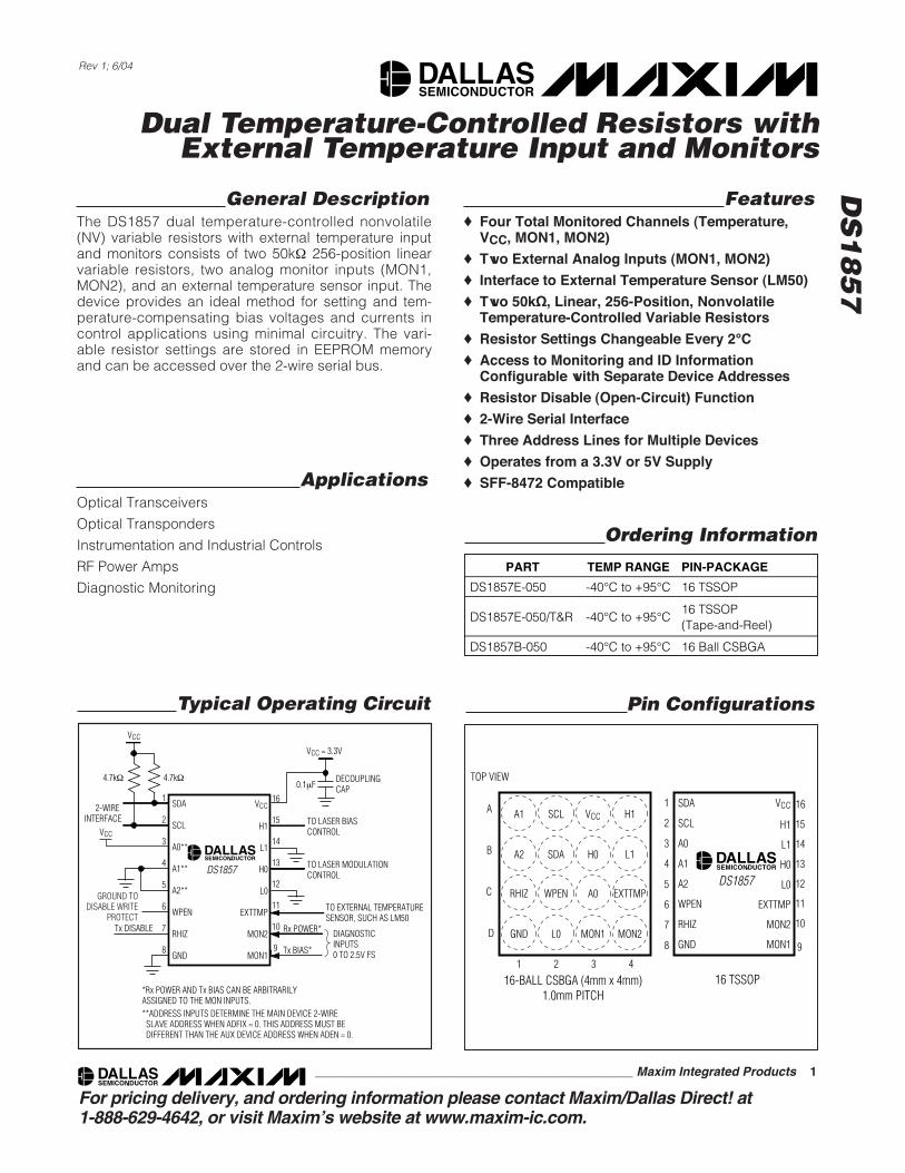
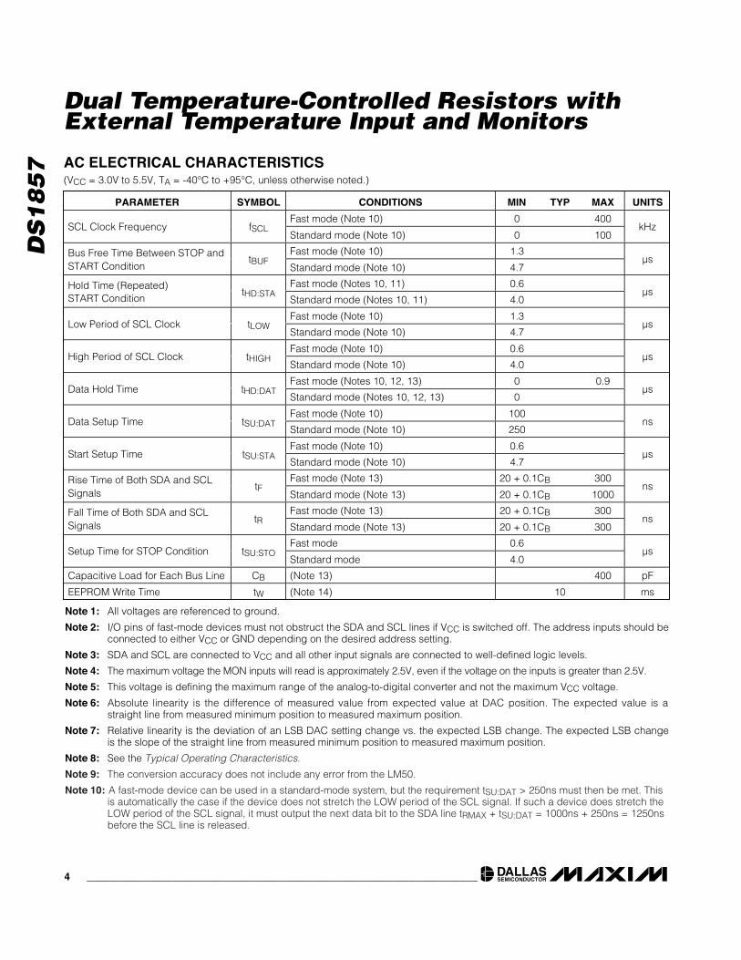
PARAMETER SYMBOL CONDITIONS MIN TYP MAX UNITS
Supply Voltage VCC (Note 1) +3.0 5.5 V
Input Logic 1 (SDA, SCL, A2, A1, A0,WPEN, RHIZ)
VIH (Note 2) 0.7 x Vcc VCC + 0.3 V
Input Logic 0 (SDA, SCL, A2, A1, A0,WPEN, RHIZ)
VIL (Note 2) -0.3 0.3 x VCC V
Resistor Inputs (L0, L1, H0, H1) -0.3 VCC + 0.3 V
Resistor Current IRES -3 +3 mA
ABSOLUTE MAXIMUM RATINGS
Stresses beyond those listed under “Absolute Maximum Ratings” may cause permanent damage to the device. These are stress ratings only, and functionaloperation of the device at these or any other conditions beyond those indicated in the operational sections of the specifications is not implied. Exposure toabsolute maximum rating conditions for extended periods may affect device reliability.
Voltage on VCC Relative to Ground.......................-0.5V to +6.0VVoltage on Inputs Relative
to Ground* ................................................-0.5V to VCC + 0.5V Voltage on Resistor Inputs Relative
to Ground* ................................................-0.5V to VCC + 0.5V Current into Resistors............................................................5mA
Operating Temperature Range ...........................-40°C to +95°C Programming Temperature Range .........................0°C to +70°CStorage Temperature Range .............................-55°C to +125°CSoldering Temperature .......................................See IPC/JEDEC
J-STD-020A Specification
RECOMMENDED DC OPERATING CONDITIONS(TA = -40°C to +95°C, unless otherwise noted.)
PARAMETER SYMBOL CONDITIONS MIN TYP MAX UNITSSupply Current ICC (Note 3) 1 2 mA
Input Leakage IIL -1 +1 µA
Input Current each I/O Pin 0.4 x VCC < VI/O < 0.9 x VCC -10 +10 µA
VOL1 3mA sink current 0 0.4Low-Level Output Voltage (SDA)
VOL2 6mA sink current 0 0.6V
Full-Scale Input (MON1, MON2) (Note 4) 2.4875 2.5000 2.5125 V
Full-Scale VCC Monitor (Note 5) 6.5208 6.5536 6.5864 V
I/O Capacitance CI/O 10 pF
WPEN Pullup Resistor RWPEN 40 65 100 kΩRHIZ Pullup Resistor RRHIZ 40 65 100 kΩDigital Power-On Reset POD 1.0 2.2 V
Analog Power-On Reset POA 2.0 2.6 V
DC ELECTRICAL CHARACTERISTICS(VCC = 3.0V to 5.5V, TA = -40°C to +95°C, unless otherwise noted.)
*Not to exceed 6.0V.
DS
18
57
Dual Temperature-Controlled Resistors withExternal Temperature Input and Monitors
_____________________________________________________________________ 3
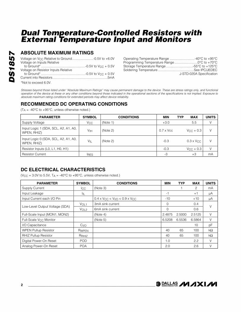
PARAMETER SYMBOL CONDITIONS MIN TYP MAX UNITS
EXTTMP Input Voltage VEXTTMP 1.779 V
Conversion Resolution ∆VEXTTMP 625 µV
Conversion Accuracy VEXTTMP (Note 9) 12.8 mV
EXTERNAL TEMPERATURE(VCC = 3.0V to 5.5V, TA = -40°C to +95°C, unless otherwise noted.)
PARAMETER SYMBOL CONDITIONS MIN TYP MAX UNITS
Input Resolution ∆VMON 610 µV
Supply Resolution ∆VCC 1.6 mV
Input/Supply Accuracy ACC 0.25 0.5% FS
(full scale)
Update Rate for MON1, MON2,Temp, or VCC
tframe 20 30 ms
ANALOG VOLTAGE MONITORING (VCC = 3.0V to 5.5V, TA = -40°C to +95°C, unless otherwise noted.)
PARAMETER SYMBOL CONDITIONS MIN TYP MAX UNITS
Position 00h Resistance TA = +25°C 0.70 1.0 1.25 kΩPosition FFh Resistance TA = +25°C 40 50 60 kΩAbsolute Linearity (Note 6) -2 +2 LSB
Relative Linearity (Note 7) -1 +1 LSB
Temperature Coefficient (Note 8) 50 ppm/°C
High-Z Resistor Current IRHIZ RHIZ = VCC 0.1 µA
ANALOG RESISTOR CHARACTERISTICS(VCC = 3.0V to 5.5V, TA = -40°C to +95°C, unless otherwise noted.)
DS
18
57
Dual Temperature-Controlled Resistors withExternal Temperature Input and Monitors
4 _____________________________________________________________________
PARAMETER SYMBOL CONDITIONS MIN TYP MAX UNITS
Fast mode (Note 10) 0 400SCL Clock Frequency fSCL
Standard mode (Note 10) 0 100kHz
Fast mode (Note 10) 1.3Bus Free Time Between STOP andSTART Condition
tBUFStandard mode (Note 10) 4.7
µs
Fast mode (Notes 10, 11) 0.6Hold Time (Repeated)START Condition
tHD:STAStandard mode (Notes 10, 11) 4.0
µs
Fast mode (Note 10) 1.3Low Period of SCL Clock tLOW
Standard mode (Note 10) 4.7µs
Fast mode (Note 10) 0.6High Period of SCL Clock tHIGH
Standard mode (Note 10) 4.0µs
Fast mode (Notes 10, 12, 13) 0 0.9Data Hold Time tHD:DAT
Standard mode (Notes 10, 12, 13) 0µs
Fast mode (Note 10) 100Data Setup Time tSU:DAT
Standard mode (Note 10) 250ns
Fast mode (Note 10) 0.6Start Setup Time tSU:STA
Standard mode (Note 10) 4.7µs
Fast mode (Note 13) 20 + 0.1CB 300Rise Time of Both SDA and SCLSignals
tFStandard mode (Note 13) 20 + 0.1CB 1000
ns
Fast mode (Note 13) 20 + 0.1CB 300Fall Time of Both SDA and SCLSignals
tRStandard mode (Note 13) 20 + 0.1CB 300
ns
Fast mode 0.6Setup Time for STOP Condition tSU:STO
Standard mode 4.0µs
Capacitive Load for Each Bus Line CB (Note 13) 400 pF
EEPROM Write Time tW (Note 14) 10 ms
AC ELECTRICAL CHARACTERISTICS(VCC = 3.0V to 5.5V, TA = -40°C to +95°C, unless otherwise noted.)
Note 1: All voltages are referenced to ground.
Note 2: I/O pins of fast-mode devices must not obstruct the SDA and SCL lines if VCC is switched off. The address inputs should beconnected to either VCC or GND depending on the desired address setting.
Note 3: SDA and SCL are connected to VCC and all other input signals are connected to well-defined logic levels.
Note 4: The maximum voltage the MON inputs will read is approximately 2.5V, even if the voltage on the inputs is greater than 2.5V.
Note 5: This voltage is defining the maximum range of the analog-to-digital converter and not the maximum VCC voltage.
Note 6: Absolute linearity is the difference of measured value from expected value at DAC position. The expected value is astraight line from measured minimum position to measured maximum position.
Note 7: Relative linearity is the deviation of an LSB DAC setting change vs. the expected LSB change. The expected LSB changeis the slope of the straight line from measured minimum position to measured maximum position.
Note 8: See the Typical Operating Characteristics.
Note 9: The conversion accuracy does not include any error from the LM50.
Note 10: A fast-mode device can be used in a standard-mode system, but the requirement tSU:DAT > 250ns must then be met. Thisis automatically the case if the device does not stretch the LOW period of the SCL signal. If such a device does stretch theLOW period of the SCL signal, it must output the next data bit to the SDA line tRMAX + tSU:DAT = 1000ns + 250ns = 1250nsbefore the SCL line is released.
DS
18
57
Dual Temperature-Controlled Resistors withExternal Temperature Input and Monitors
_____________________________________________________________________ 5
AC ELECTRICAL CHARACTERISTICS (continued)(VCC = 3.0V to 5.5V, TA = -40°C to +95°C, unless otherwise noted.)
Note 11: After this period, the first clock pulse is generated.
Note 12: The maximum tHD:DAT only to has be met if the device does not stretch the LOW period (tLOW) of the SCL signal.
Note 13: A device must internally provide a hold time of at least 300ns for the SDA signal (see the VIH MIN of the SCL signal) in orderto bridge the undefined region of the falling edge of SCL.
Note 14: CB—total capacitance of one bus line, timing referenced to 0.9 x VCC and 0.1 x VCC.
Note 15: EEPROM write begins after a STOP condition occurs.
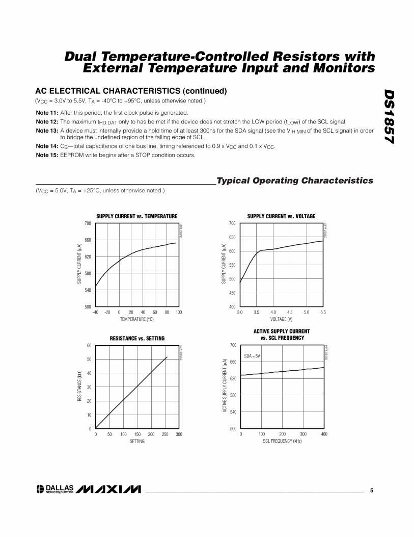
Typical Operating Characteristics(VCC = 5.0V, TA = +25°C, unless otherwise noted.)
SUPPLY CURRENT vs. TEMPERATURE
DS18
57 to
c01
TEMPERATURE (°C)
SUPP
LY C
URRE
NT (µ
A)
806040200-20
540
580
620
660
700
500-40 100
SUPPLY CURRENT vs. VOLTAGE
DS18
57 to
c02
VOLTAGE (V)
SUPP
LY C
URRE
NT (µ
A)
5.04.54.03.5
450
500
550
600
650
700
4003.0 5.5
RESISTANCE vs. SETTING
DS18
57 to
c03
SETTING
RESI
STAN
CE (kΩ
)
25020015010050
10
20
30
40
50
60
00 300
ACTIVE SUPPLY CURRENT vs. SCL FREQUENCY
DS18
57 to
c04
SCL FREQUENCY (kHz)
ACTI
VE S
UPPL
Y CU
RREN
T (µ
A)
300200100
540
580
620
660
700
5000 400
SDA = 5V
DS
18
57
Dual Temperature-Controlled Resistors withExternal Temperature Input and Monitors
6 _____________________________________________________________________
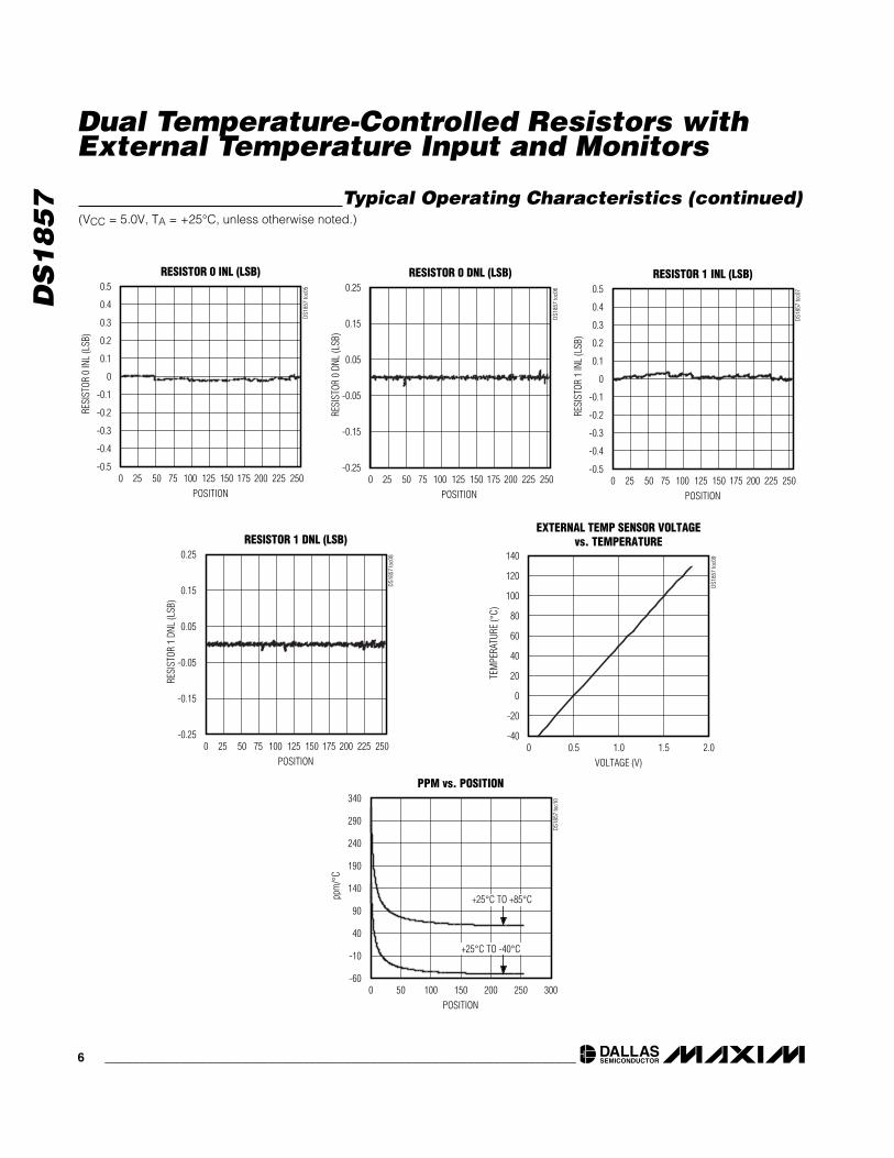
Typical Operating Characteristics (continued)(VCC = 5.0V, TA = +25°C, unless otherwise noted.)
RESISTOR 0 INL (LSB)
DS18
57 to
c05
POSITION
RESI
STOR
0 IN
L (L
SB)
225200150 17550 75 100 12525
-0.4
-0.3
-0.2
-0.1
0
0.1
0.2
0.3
0.4
0.5
-0.50 250
RESISTOR 0 DNL (LSB)
DS18
57 to
c06
RESI
STOR
0 D
NL (L
SB)
-0.15
-0.05
0.05
0.15
0.25
-0.25
POSITION 225200150 17550 75 100 125250 250
RESISTOR 1 INL (LSB)
DS18
57 to
c07
POSITION
RESI
STOR
1 IN
L (L
SB)
225200150 17550 75 100 12525
-0.4
-0.3
-0.2
-0.1
0
0.1
0.2
0.3
0.4
0.5
-0.50 250
RESISTOR 1 DNL (LSB)
DS18
57 to
c08
RESI
STOR
1 D
NL (L
SB)
-0.15
-0.05
0.05
0.15
0.25
-0.25
POSITION225200150 17550 75 100 125250 250
EXTERNAL TEMP SENSOR VOLTAGEvs. TEMPERATURE
DS18
57 to
c09
VOLTAGE (V)
TEM
PERA
TURE
(°C)
1.51.00.5
-20
0
20
40
60
80
100
120
140
-400 2.0
PPM vs. POSITION
DS18
57 to
c10
POSITION
ppm
/°C
25020050 100 150
-10
40
90
140
190
240
290
340
-600 300
+25°C TO +85°C
+25°C TO -40°C
DS
18
57
Dual Temperature-Controlled Resistors withExternal Temperature Input and Monitors
_____________________________________________________________________ 7
Detailed DescriptionThe user can read the registers that monitor the VCC,MON1, MON2, and temperature analog signals. Aftereach signal conversion, a corresponding bit is set thatcan be monitored to verify that a conversion hasoccurred. The signals also have alarm flags that notifythe user when the signals go above or below the user-defined value. Interrupts can also be set for each signal.
The position values of each resistor can be indepen-dently programmed. The user can assign a uniquevalue to each resistor for every 2°C increment over the-40°C to +102°C range. Both resistors can also be putin a high-impedance mode using the RHIZ pin.
An external temperature sense input, EXTTMP, con-verts an analog voltage into a digital value that repre-sents temperature. Its scale is defined by +10mV/°Cgain and +500mV offset at 0°C. This corresponds to thecharacteristics of the LM50 temperature sensor. Theresistor look-up tables are stepped through accordingto this temperature every 2°C from -40°C to +102°C.
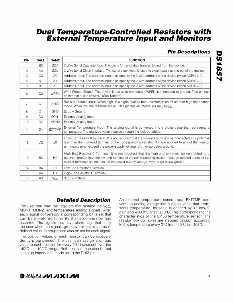
PIN BALL NAME FUNCTION
1 B2 SDA 2-Wire Serial Data Interface. This pin is for serial data transfer to and from the device.
2 A2 SCL 2-Wire Serial Clock Interface. The serial clock input is used to clock data into and out of the device.
3 C3 A0 Address Input. The address input pins specify the 2-wire address of the device (when ADFIX = 0).
4 A1 A1 Address Input. The address input pins specify the 2-wire address of the device (when ADFIX = 0).
5 B1 A2 Address Input. The address input pins specify the 2-wire address of the device (when ADFIX = 0).
6 C2 WPENWrite Protect Enable. The device is not write protected if WPEN is connected to ground. This pin hasan internal pullup (RWPEN) (See Table 6).
7 C1 RHIZResistor Disable Input. When high, this signal places both resistors in an off state or high impedancemode. When low, the resistors are on. This pin has an internal pullup (RRHIZ).
8 D1 GND Supply Ground
9 D3 MON1 External Analog Input
10 D4 MON2 External Analog Input
11 C4 EXTTMPExternal Temperature Input. This analog signal is converted into a digital value that represents atemperature. The digitized value indexes through the look-up tables.
12 D2 L0Low-End Resistor 0 Terminal. It is not required that the low-end terminals be connected to a potentialless than the high-end terminal of the corresponding resistor. Voltage applied to any of the resistorterminals cannot exceed the power-supply voltage, VCC, or go below ground.
13 B3 H0High-End Resistor 0 Terminal. It is not required that the high-end terminals be connected to apotential greater than the low-end terminal of the corresponding resistor. Voltage applied to any of theresistor terminals cannot exceed the power-supply voltage, VCC, or go below ground.
14 B4 L1 Low-End Resistor 1 Terminal
15 A4 H1 High-End Resistor 1 Terminal.
16 A3 VCC Supply Voltage
Pin Descriptions
DS
18
57
Dual Temperature-Controlled Resistors withExternal Temperature Input and Monitors
8 _____________________________________________________________________
DEVICEADDRESS
AD (AUXILIARY DEVICE ENABLE A0h)
MD (MAIN DEVICE ENABLE)
DEVICE ADDRESS
ADDRESS
ADDRESS
ADDRESS
R/W
R/W
DATA BUS
R/W
ADEN ADFIX
SDA
SCL
2-WIREINTERFACE
RHIZ
MON1
MON2
VCC
GND
WPEN
EEPROM128 x 8 BIT
00h-7Fh
STANDARDS
PROTAUX AD
ADDRESS
TABLESELECT
R/W
EEPROM72 x 8 BIT80h-C7h
TABLE 02RESISTOR 0LOOK-UP
TABLE
PROTMAIN MD
EEPROM72 x 8 BIT80h-C7h
SRAM32 x 8 BIT60h-7Fh
NOT PROTECTED
PROTMAIN MD
TEMP INDEX
ALARM FLAGS
MUXCTRL
MEASUREMENT
ADDRESS
TABLESELECT
R/W
EEPROM72 x 8 BIT80h-C7h
TABLE 03RESISTOR 1LOOK-UP
TABLE
PROTMAIN MD
TEMP INDEX
VCC
RRHIZ
RWPEN
MONITORS LIMITHIGH
MONITORS LIMITLOW
TABLE SELECT
TEMP INDEX
MINT (BIT)
EXTTMPVCC
MUXA/D
12-BIT
A/DCTRL
VCCVCC
PROT AUX
PROT MAIN
MPEN
APEN
COMPARATOR
MEASUREMENT
ALARM FLAGS
MONITORS LIMIT LOW
MONITORS LIMIT HIGH
COMP CTRLINTERRUPT
MINT
TABLE 01EEPROM16 x 8 BIT80h-8Fh
VENDOR
PROTMAIN MD R/W
DEVICE ADDRESS
ADDRESS
TABLE SELECT
MASKING (TMP, VCC, MON1, MON2)
ADFIX (BIT)
ADEN (BIT)
MPEN (BIT)
APEN (BIT)
INV2 (BIT)
INV1 (BIT)
RHIZ
RESISTOR 050kΩ FULL SCALE
256 POSITIONS
L0
H0
REGI
STER
REGI
STER
RHIZ
RESISTOR 150kΩ FULL SCALE
256 POSITIONS
L1
H1
A0
A1
A2
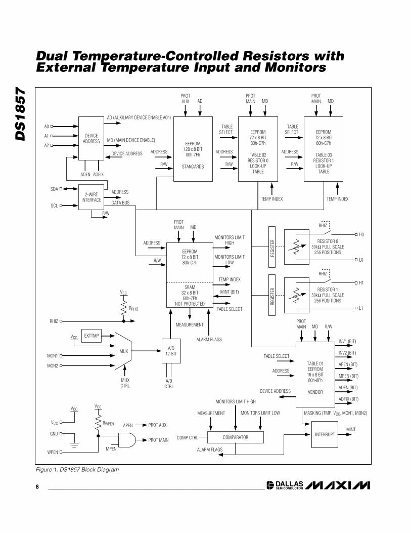
Figure 1. DS1857 Block Diagram
DS
18
57
Dual Temperature-Controlled Resistors withExternal Temperature Input and Monitors
_____________________________________________________________________ 9
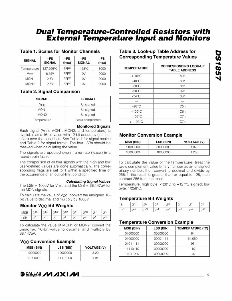
Monitored SignalsEach signal (VCC, MON1, MON2, and temperature) isavailable as a 16-bit value with 12-bit accuracy (left-jus-tified) over the serial bus. See Table 1 for signal scalesand Table 2 for signal format. The four LSBs should bemasked when calculating the value.
The signals are updated every frame rate (tframe) in around-robin fashion.
The comparison of all four signals with the high and lowuser-defined values are done automatically. The corre-sponding flags are set to 1 within a specified time ofthe occurrence of an out-of-limit condition.
Calculating Signal ValuesThe LSB = 100µV for VCC, and the LSB = 38.147µV forthe MON signals.
To calculate the value of VCC, convert the unsigned 16-bit value to decimal and multiply by 100µV.
To calculate the value of MON1 or MON2, convert theunsigned 16-bit value to decimal and multiply by38.147µV.
To calculate the value of the temperature, treat thetwo’s complement value binary number as an unsignedbinary number, then convert to decimal and divide by256. If the result is greater than or equal to 128, thensubtract 256 from the result.
Temperature: high byte: -128°C to +127°C signed; lowbyte: 1/256°C.
SIGNAL+FS
SIGNAL+FS(hex)
-FSSIGNAL
-FS(hex)
Temperature 127.996°C 7FFF -128°C 8000
VCC 6.55V FFFF 0V 0000
MON1 2.5V FFFF 0V 0000
MON2 2.5V FFFF 0V 0000
Table 1. Scales for Monitor Channels
SIGNAL FORMAT
VCC Unsigned
MON1 Unsigned
MON2 Unsigned
Temperature Two’s complement
Table 2. Signal Comparison
TEMPERATURECORRESPONDING LOOK-UP
TABLE ADDRESS
<-40°C 80h
-40°C 80h
-38°C 81h
-36°C 82h
-34°C 83h
— —
+98°C C5h
+100°C C6h
+102°C C7h
>+102°C C7h
Table 3. Look-up Table Address forCorresponding Temperature Values
MSB 215 214 213 212 211 210 29 28
LSB 27 26 25 24 23 22 21 20
MSB (BIN) LSB (BIN) VOLTAGE (V)
10000000 10000000 3.29
11000000 11111000 4.94
S 26 25 24 23 22 21 20
2-1 2-2 2-3 2-4 2-5 2-6 2-7 2-8
MSB (BIN) LSB (BIN) TEMPERATURE (°C)
01000000 00000000 64
01000000 00001111 64.059
01011111 00000000 95
11110110 00000000 -10
11011000 00000000 -40
MSB (BIN) LSB (BIN) VOLTAGE (V)
11000000 00000000 1.875
10000000 10000000 1.255
Monitor VCC Bit Weights
Temperature Bit Weights
Temperature Conversion Example
VCC Conversion Example
Monitor Conversion Example
DS
18
57
Dual Temperature-Controlled Resistors withExternal Temperature Input and Monitors
10 ____________________________________________________________________
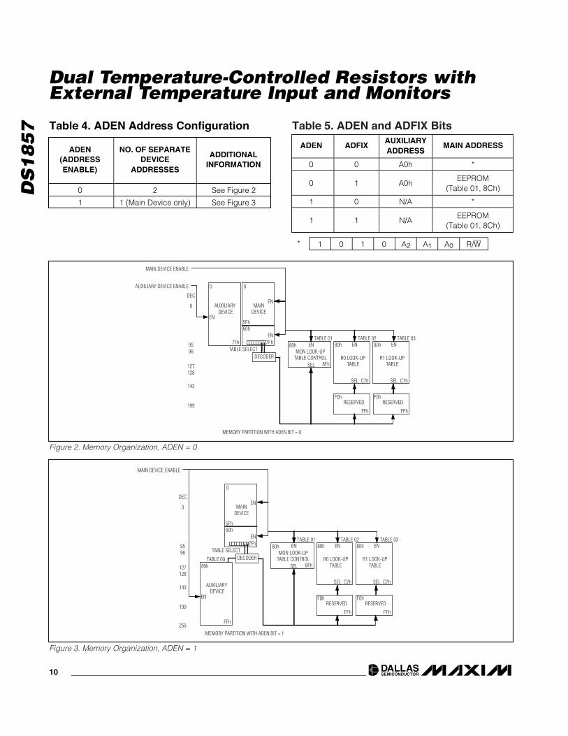
ADEN(ADDRESSENABLE)
NO. OF SEPARATEDEVICE
ADDRESSES
ADDITIONALINFORMATION
0 2 See Figure 2
1 1 (Main Device only) See Figure 3
Table 4. ADEN Address Configuration
ADEN ADFIXAUXILIARYADDRESS
MAIN ADDRESS
0 0 A0h *
0 1 A0hEEPROM
(Table 01, 8Ch)
1 0 N/A *
1 1 N/AEEPROM
(Table 01, 8Ch)
Table 5. ADEN and ADFIX Bits
MAINDEVICE
MON LOOK-UPTABLE CONTROL R0 LOOK-UP
TABLE
AUXILIARY DEVICE
0
DEC
0
9596
127128
143
199
MEMORY PARTITION WITH ADEN BIT = 0
EN
EN
EN
EN
SEL
EN
SEL
7Fh 7Fh 80h 80h
60h
C7h
F0h
FFh
RESERVED RESERVED
8Fh
5Fh
TABLE SELECT
MAIN DEVICE ENABLE
AUXILIARY DEVICE ENABLE
DECODER
0
F0h
FFh
R1 LOOK-UPTABLE
EN
SEL
80h
C7h
TABLE 03TABLE 02TABLE 01
Figure 2. Memory Organization, ADEN = 0
MAINDEVICE
MON LOOK-UPTABLE CONTROL R0 LOOK-UP
TABLE
AUXILIARY DEVICE
80h
DEC
0
9596
127128
143
199
255
EN
EN
EN
EN
SEL
EN
SEL
FFh
7Fh 80h 80h
C7h
F0h
FFh
RESERVED RESERVED
8Fh
TABLE SELECT
TABLE 00
MAIN DEVICE ENABLE
DECODER
0
F0h
FFh
R1 LOOK-UPTABLE
EN
SEL
80h
C7h
TABLE 03TABLE 02TABLE 01
MEMORY PARTITION WITH ADEN BIT = 1
60h5Fh
Figure 3. Memory Organization, ADEN = 1
* 1 0 1 0 A2 A1 A0 R/W
DS
18
57
Dual Temperature-Controlled Resistors withExternal Temperature Input and Monitors
____________________________________________________________________ 11
Variable ResistorsThe value of each variable resistor is determined by atemperature-addressed look-up table, which canassign a unique value (00h to FFh) to each resistor forevery 2°C increment over the -40°C to +102°C range(see Table 3). See the Temperature Conversion sectionfor more information.
A resistor disable feature places both outputs in a high-impedance mode. This occurs when the RHIZ input ishigh. An internal pullup of RRHIZ is provided, readyingthis pin for input from the Tx Disable signal as specifiedin the SFF and SFP MSA.The variable resistors can also be used in manualmode. If the TEN bit equals 0, then the resistors are inmanual mode and the temperature indexing is dis-abled. The user sets the resistors in manual mode bywriting to addresses 82h and 83h in Table 01 to controlresistors 0 and 1, respectively.
Memory DescriptionMain and auxiliary memories can be accessed by twoseparate device addresses. The Main Device addressis determined by address pins or value in Table 01 byte8Ch, when ADFIX = 1 (see Table 5). The AuxiliaryDevice address is A0h. A user option is provided torespond to one or two device addresses. This featurecan be used to save component count in SFF applica-tions (Main Device address can be used) or otherapplications where both GBIC (Auxiliary Deviceaddress can be used) and monitoring functions areimplemented and two device addresses are needed.The memory blocks are enabled with the correspond-ing device address. Memory space from 80h and up isaccessible only through the Main Device address. Thismemory is organized as three tables; the desired tablecan be selected by the contents of memory location7Fh, Main Device. The Auxiliary Device address has noaccess to the tables, but the Auxiliary Device addresscan be mapped into the Main Device’s memory spaceas a fourth table. Device addresses are programmablewith two control bits in EEPROM.
ADEN configures memory access to respond to differ-ent device addresses (see Tables 4 and 5).
The default device address for EEPROM-generatedaddresses is A2h.
If the ADEN bit is 1, additional 128 bytes of EEPROMare accessible through the Main Device, selected asTable 00 (see Figure 3). In this configuration, theAuxiliary Device address is not accessible. APEN con-trols the direction of Table 00 regardless of the settingof ADEN.
ADFIX (address fixed) determines whether the MainDevice address is determined by an EEPROM byte(Table 01, byte 8Ch, when ADFIX =1). There can be upto 128 devices sharing a common 2-wire bus, witheach device having its own unique device address.
Memory ProtectionMemory access from either device address can beeither read/write or read only. Write protection isaccomplished by a combination of control bits in EEPROM (APEN and MPEN in configuration register89h) and a write-protect enable (WPEN) pin. Since theWPEN pin is often not accessible from outside the mod-ule, this scheme effectively allows the module to belocked by the manufacturer to prevent accidental writesby the end user.Separate write protection is provided for the Auxiliaryand Main Device address through distinct bits APENand MPEN. APEN and MPEN are bits from configura-tion register 89h, Table 01. Due to the location, theAPEN and MPEN bits can only be written through theMain Device address. The control of write privilegesthrough the Auxiliary Device address is dependent onthe value of APEN. Care should be taken with the set-ting of MPEN, once set to a 1, assuming WPEN is high,access through the Main Device is thereafter deniedunless WPEN is taken to a low level. By this meansinadvertent end-user write access can be denied.Main Device address space 60h to 7Fh is SRAM and isnot write protected by APEN, MPEN, or WPEN. Forexample, the user may reset flags set by the device.Bytes designated as “Reserved” may be used asscratchpad but they will not be stored in a power cyclebecause of their volatility. These bytes are reserved foradded functionality in future versions of this device.Note that in single device mode (ADEN bit = 1), APENdetermines the protection level of Table 00, indepen-dent of WPEN.The write-protect operation, for both Main and AuxiliaryDevices, is summarized in Tables 6 and 7.
WPEN MPEN PROTECT MAIN
0 X No
X 0 No
1 1 Yes
Table 6. Main Device
APEN WPEN PROTECT AUXILIARY
0 X No
1 X Yes
Table 7. Auxiliary Device
DS
18
57 Register Map
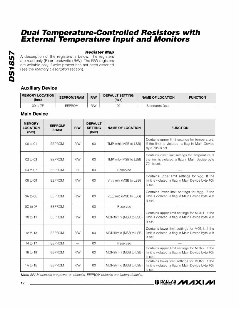
A description of the registers is below. The registersare read only (R) or read/write (R/W). The R/W registersare writable only if write protect has not been asserted(see the Memory Description section).
Dual Temperature-Controlled Resistors withExternal Temperature Input and Monitors
12 ____________________________________________________________________
MEMORY LOCATION(hex)
EEPROM/SRAM R/WDEFAULT SETTING
(hex)NAME OF LOCATION FUNCTION
00 to 7F EEPROM R/W 00 Standards Data —
Auxiliary Device
MEMORYLOCATION
(hex)
EEPROM/SRAM
R/WDEFAULTSETTING
(hex)NAME OF LOCATION FUNCTION
00 to 01 EEPROM R/W 00 TMPlimhi (MSB to LSB)Contains upper limit settings for temperature.If the limit is violated, a flag in Main Devicebyte 70h is set.
02 to 03 EEPROM R/W 00 TMPlimlo (MSB to LSB)Contains lower limit settings for temperature. Ifthe limit is violated, a flag in Main Device byte70h is set.
04 to 07 EEPROM R 00 Reserved —
08 to 09 EEPROM R/W 00 VCClimhi (MSB to LSB)Contains upper limit settings for VCC. If thelimit is violated, a flag in Main Device byte 70his set.
0A to 0B EEPROM R/W 00 VCClimlo (MSB to LSB)Contains lower limit settings for VCC. If thelimit is violated, a flag in Main Device byte 70his set.
0C to 0F EEPROM — 00 Reserved —
10 to 11 EEPROM R/W 00 MON1limhi (MSB to LSB)Contains upper limit settings for MON1. If thelimit is violated, a flag in Main Device byte 70his set.
12 to 13 EEPROM R/W 00 MON1limlo (MSB to LSB)Contains lower limit settings for MON1. If thelimit is violated, a flag in Main Device byte 70his set.
14 to 17 EEPROM — 00 Reserved —
18 to 19 EEPROM R/W 00 MON2limhi (MSB to LSB)Contains upper limit settings for MON2. If thelimit is violated, a flag in Main Device byte 70his set.
1A to 1B EEPROM R/W 00 MON2limlo (MSB to LSB)Contains lower limit settings for MON2. If thelimit is violated, a flag in Main Device byte 70his set.
Main Device
Note: SRAM defaults are power-on defaults. EEPROM defaults are factory defaults.
DS
18
57
Dual Temperature-Controlled Resistors withExternal Temperature Input and Monitors
____________________________________________________________________ 13
MEMORYLOCATION
(hex)
EEPROM/SRAM
R/WDEFAULTSETTING
(hex)NAME OF LOCATION FUNCTION
1C to 5F EEPROM — 00 Reserved —
60 to 61 SRAM R —Measured TMP(MSB to LSB)
Digitized measured value for temperature.See Table 1.
62 to 63 SRAM R —Measured VCC(MSB to LSB)
Digitized measured value for VCC.See Table 1.
64 to 65 SRAM R —Measured MON1
(MSB to LSB)Digitized measured value for MON1.See Table 1.
66 to 67 SRAM R —Measured MON2
(MSB to LSB)Digitized measured value for MON2.See Table 1.
68 to 6D SRAM R — Reserved —
6E SRAM — — Logic states —
Bit 7 — R X HIZSTA
Resistor status bit. A high indicates that bothresistors are in high-impedance mode. A lowindicates that both resistors are operatingnormally.
6 — R/W 0 HIZCOResistor control bit. Setting this bit highcauses both resistors to go into a high-impedance state.
5 — — X X —
4 — — X X —
3 — — X X —
2 — — X X —
1 — — X X —
0 — R X RDYBThis status bit goes high when VCC has fallenbelow the POA level.
6F SRAM — — Conversion updates —
Bit 7 — R/W 0 TAU
This bit goes high after a temperature andaddress update has occurred for thecorresponding measurement in bytes 60h to61h. This bit can be written to a 0 by the userand monitored to verify that a conversion hasoccurred.
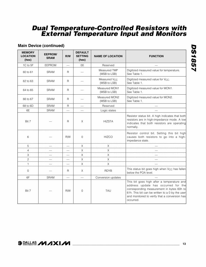
Main Device (continued)
DS
18
57
Dual Temperature-Controlled Resistors withExternal Temperature Input and Monitors
14 ____________________________________________________________________
MEMORYLOCATION
(hex)
EEPROM/SRAM
R/WDEFAULTSETTING
(hex)NAME OF LOCATION FUNCTION
6 — R/W 0 VCCU
This bit goes high after a VCC update hasoccurred for the corresponding measurementin bytes 62h to 63h. This bit can be written toa 0 by the user and monitored to verify that aconversion has occurred.
5 — R/W 0 MON1U
This bit goes high after a MON1 update hasoccurred for the corresponding measurementin bytes 64h to 65h. This bit can be written toa 0 by the user and monitored to verify that aconversion has occurred.
4 — R/W 0 MON2U
This bit goes high after a MON2 update hasoccurred for the corresponding measurementin bytes 66h to 67h. This bit can be written toa 0 by the user and monitored to verify that aconversion has occurred.
3 — — 0 0 —
2 — — 0 0 —
1 — — 0 X —
0 — — 0 X —
70 SRAM R — Alarm flags —
Bit 7 — — — TMPhiThis alarm flag goes high when the upper limitof the temperature setting is violated.
6 — — — TMPloThis alarm flag goes high when the lower limitof the temperature setting is violated.
5 — — — VCChiThis alarm flag goes high when the upper limitof the VCC setting is violated.
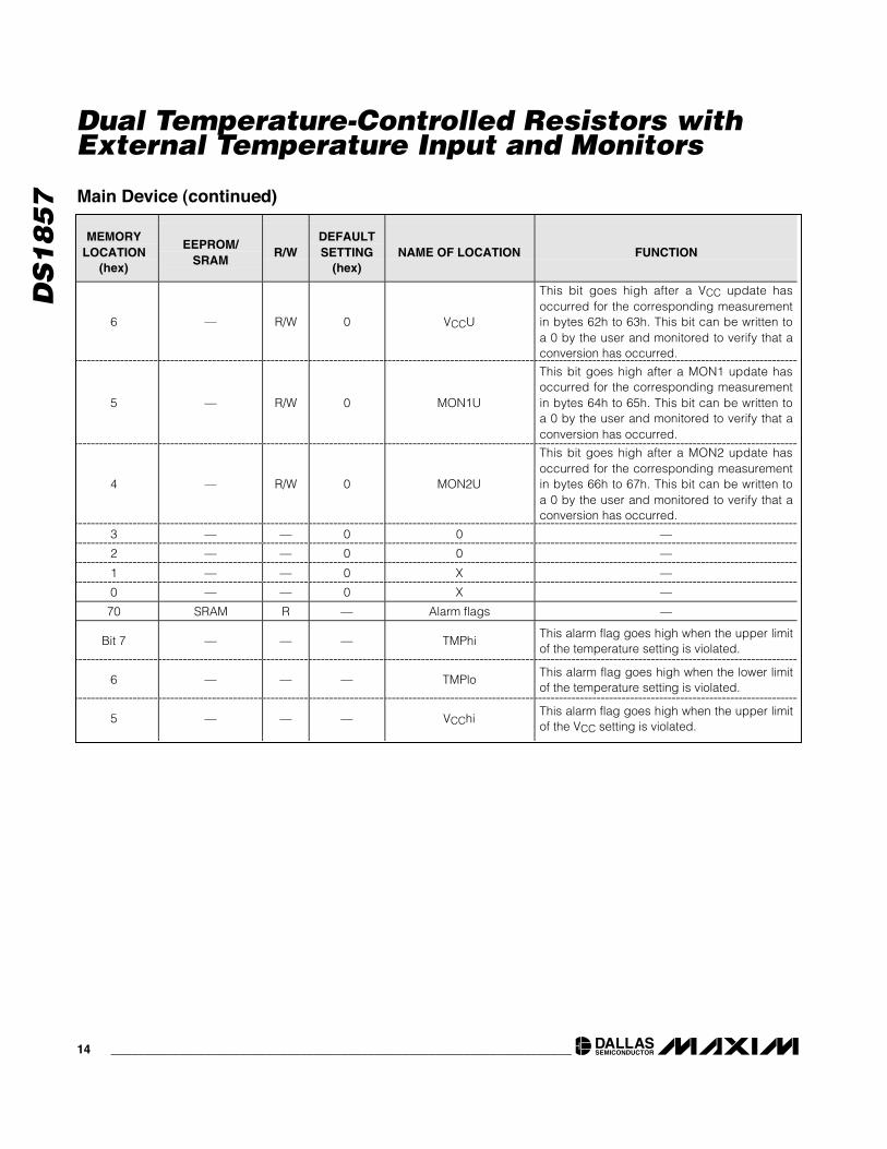
Main Device (continued)
DS
18
57
Dual Temperature-Controlled Resistors withExternal Temperature Input and Monitors
____________________________________________________________________ 15
MEMORYLOCATION
(hex)
EEPROM/SRAM
R/WDEFAULTSETTING
(hex)NAME OF LOCATION FUNCTION
4 — — — VCCloThis alarm flag goes high when the lower limitof the VCC setting is violated.
3 — — — MON1hiThis alarm flag goes high when the upper limitof the MON1 setting is violated.
2 — — — MON1loThis alarm flag goes high when the lower limitof the MON1 setting is violated.
1 — — — MON2hiThis alarm flag goes high when the upper limitof the MON2 setting is violated.
0 — — — MON2loThis alarm flag goes high when the lower limitof the MON2 setting is violated.
71 SRAM R — Alarm flags —
Bit 7 — — — X —
6 — — — X —
5 — — — X —
4 — — — X —
3 — — — X —
2 — — — X —
1 — — — X —
0 — — — MINT
A mask of all flags located in Table 01 byte88h determines the value of MINT. MINT ismaskable to 0 if no interrupt is desired bysetting Table 01 byte 88h to 0.
72 to 7E SRAM R 00 Reserved —
7F SRAM R/W Table select —
Bit 7 — — 0 X —
6 — — 0 X —
5 — — 0 X —
4 — — 0 X —
3 — — 0 X —
2 — — 0 X —
1 — — 0
0 — — 0Table select bits
Set bits = 00 to select Table 00, set bits = 01to select Table 01, set bits = 10 to selectTable 02, set bits = 11 to select Table 03.
Main Device (continued)
DS
18
57
Dual Temperature-Controlled Resistors withExternal Temperature Input and Monitors
16 ____________________________________________________________________
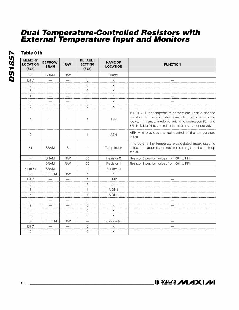
MEMORYLOCATION
(hex)
EEPROM/SRAM
R/WDEFAULTSETTING
(hex)
NAME OFLOCATION
FUNCTION
80 SRAM R/W Mode —
Bit 7 — — 0 X —
6 — — 0 X —
5 — — 0 X —
4 — — 0 X —
3 — — 0 X —
2 — — 0 X —
1 — — 1 TEN
If TEN = 0, the temperature conversions update and theresistors can be controlled manually. The user sets theresistor in manual mode by writing to addresses 82h and83h in Table 01 to control resistors 0 and 1, respectively.
0 — — 1 AENAEN = 0 provides manual control of the temperatureindex.
81 SRAM R — Temp indexThis byte is the temperature-calculated index used toselect the address of resistor settings in the look-uptables.
82 SRAM R/W 00 Resistor 0 Resistor 0 position values from 00h to FFh.83 SRAM R/W 00 Resistor 1 Resistor 1 position values from 00h to FFh.
84 to 87 SRAM — 00 Reserved —
88 EEPROM R/W X X —
Bit 7 — — 1 TMP —
6 — — 1 VCC —
5 — — 1 MON1 —
4 — — 1 MON2 —
3 — — 0 X —
2 — — 0 X —
1 — — 0 X —
0 — — 0 X —
89 EEPROM R/W — Configuration —
Bit 7 — — 0 X —
6 — — 0 X —
Table 01h
DS
18
57
Dual Temperature-Controlled Resistors withExternal Temperature Input and Monitors
____________________________________________________________________ 17
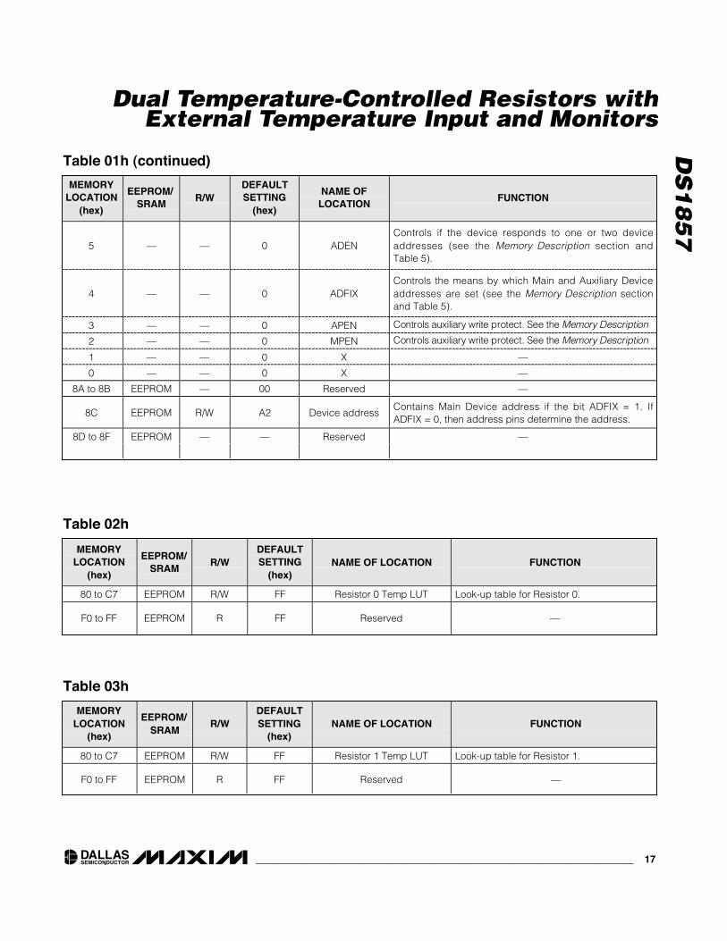
MEMORYLOCATION
(hex)
EEPROM/SRAM
R/WDEFAULTSETTING
(hex)
NAME OFLOCATION
FUNCTION
5 — — 0 ADENControls if the device responds to one or two deviceaddresses (see the Memory Description section andTable 5).
4 — — 0 ADFIXControls the means by which Main and Auxiliary Deviceaddresses are set (see the Memory Description sectionand Table 5).
3 — — 0 APEN C ontr ol s auxi l i ar y w r i te p r otect. S ee the M em or y D escr i p ti on
2 — — 0 MPEN C ontr ol s auxi l i ar y w r i te p r otect. S ee the M em or y D escr i p ti on
1 — — 0 X —
0 — — 0 X —
8A to 8B EEPROM — 00 Reserved —
8C EEPROM R/W A2 Device addressContains Main Device address if the bit ADFIX = 1. IfADFIX = 0, then address pins determine the address.
8D to 8F EEPROM — — Reserved —
Table 01h (continued)
MEMORYLOCATION
(hex)
EEPROM/SRAM
R/WDEFAULTSETTING
(hex)NAME OF LOCATION FUNCTION
80 to C7 EEPROM R/W FF Resistor 0 Temp LUT Look-up table for Resistor 0.
F0 to FF EEPROM R FF Reserved —
Table 02h
MEMORYLOCATION
(hex)
EEPROM/SRAM
R/WDEFAULTSETTING
(hex)NAME OF LOCATION FUNCTION
80 to C7 EEPROM R/W FF Resistor 1 Temp LUT Look-up table for Resistor 1.
F0 to FF EEPROM R FF Reserved —
Table 03h
DS
18
57
Dual Temperature-Controlled Resistors withExternal Temperature Input and Monitors
18 ____________________________________________________________________
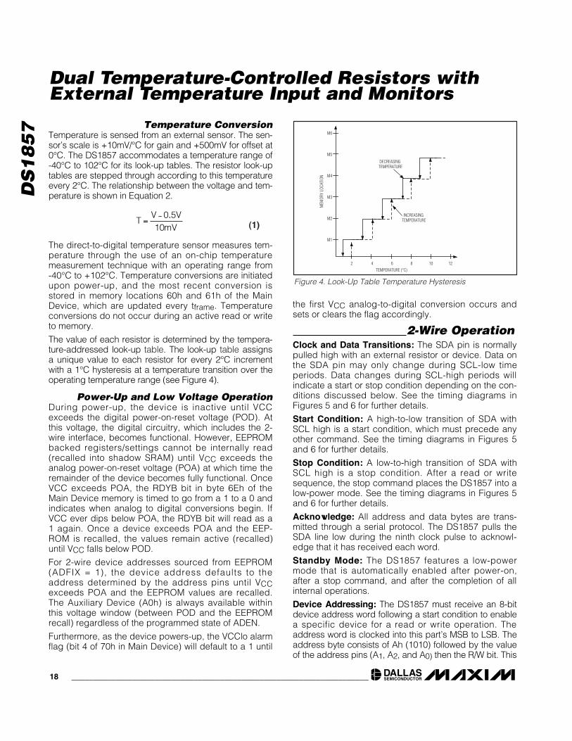
Temperature ConversionTemperature is sensed from an external sensor. The sen-sor’s scale is +10mV/°C for gain and +500mV for offset at0°C. The DS1857 accommodates a temperature range of-40°C to 102°C for its look-up tables. The resistor look-uptables are stepped through according to this temperatureevery 2°C. The relationship between the voltage and tem-perature is shown in Equation 2.
The direct-to-digital temperature sensor measures tem-perature through the use of an on-chip temperaturemeasurement technique with an operating range from -40°C to +102°C. Temperature conversions are initiatedupon power-up, and the most recent conversion isstored in memory locations 60h and 61h of the MainDevice, which are updated every tframe. Temperatureconversions do not occur during an active read or writeto memory.
The value of each resistor is determined by the tempera-ture-addressed look-up table. The look-up table assignsa unique value to each resistor for every 2°C incrementwith a 1°C hysteresis at a temperature transition over theoperating temperature range (see Figure 4).
Power-Up and Low Voltage OperationDuring power-up, the device is inactive until VCCexceeds the digital power-on-reset voltage (POD). Atthis voltage, the digital circuitry, which includes the 2-wire interface, becomes functional. However, EEPROMbacked registers/settings cannot be internally read(recalled into shadow SRAM) until VCC exceeds theanalog power-on-reset voltage (POA) at which time theremainder of the device becomes fully functional. OnceVCC exceeds POA, the RDYB bit in byte 6Eh of theMain Device memory is timed to go from a 1 to a 0 andindicates when analog to digital conversions begin. IfVCC ever dips below POA, the RDYB bit will read as a1 again. Once a device exceeds POA and the EEP-ROM is recalled, the values remain active (recalled)until VCC falls below POD.
For 2-wire device addresses sourced from EEPROM(ADFIX = 1), the device address defaults to theaddress determined by the address pins until VCCexceeds POA and the EEPROM values are recalled.The Auxiliary Device (A0h) is always available withinthis voltage window (between POD and the EEPROMrecall) regardless of the programmed state of ADEN.
Furthermore, as the device powers-up, the VCClo alarmflag (bit 4 of 70h in Main Device) will default to a 1 until
the first VCC analog-to-digital conversion occurs andsets or clears the flag accordingly.
2-Wire OperationClock and Data Transitions: The SDA pin is normallypulled high with an external resistor or device. Data onthe SDA pin may only change during SCL-low timeperiods. Data changes during SCL-high periods willindicate a start or stop condition depending on the con-ditions discussed below. See the timing diagrams inFigures 5 and 6 for further details.
Start Condition: A high-to-low transition of SDA withSCL high is a start condition, which must precede anyother command. See the timing diagrams in Figures 5and 6 for further details.
Stop Condition: A low-to-high transition of SDA withSCL high is a stop condition. After a read or writesequence, the stop command places the DS1857 into alow-power mode. See the timing diagrams in Figures 5and 6 for further details.
Acknowledge: All address and data bytes are trans-mitted through a serial protocol. The DS1857 pulls theSDA line low during the ninth clock pulse to acknowl-edge that it has received each word.
Standby Mode: The DS1857 features a low-powermode that is automatically enabled after power-on,after a stop command, and after the completion of allinternal operations.
Device Addressing: The DS1857 must receive an 8-bitdevice address word following a start condition to enablea specific device for a read or write operation. Theaddress word is clocked into this part’s MSB to LSB. Theaddress byte consists of Ah (1010) followed by the valueof the address pins (A1, A2, and A0) then the R/W bit. This
TV V
mV=
− 0 510
.(1)
M6
M5
M4
M3
M2
M1
2 4 6 8 10 12TEMPERATURE (°C)
MEM
ORY
LOCA
TION
INCREASING TEMPERATURE
DECREASING TEMPERATURE
Figure 4. Look-Up Table Temperature Hysteresis
DS
18
57
Dual Temperature-Controlled Resistors withExternal Temperature Input and Monitors
____________________________________________________________________ 19
byte must match the address programmed into Table 018Ch or A0h (for the Auxiliary Device). If a device addressmatch occurs, this part will output a zero for one clockcycle as an acknowledge and the corresponding block ofmemory is enabled (see the Memory Organization sec-tion). If the R/W bit is high, a read operation is initiated. Ifthe R/W is low, a write operation is initiated (see theMemory Organization section). If the address does notmatch, this part returns to a low-power mode.
Write OperationsAfter receiving a matching address byte with the R/Wbit set low, provided there is no write protect, thedevice goes into the write mode of operation (see theMemory Organization section). The master must trans-mit an 8-bit EEPROM memory address to the device todefine the address where the data is to be written. Afterthe byte has been received, the DS1857 transmits azero for one clock cycle to acknowledge the addresshas been received. The master must then transmit an8-bit data word to be written into this address. TheDS1857 again transmits a zero for one clock cycle toacknowledge the receipt of the data. At this point, themaster must terminate the write operation with a stopcondition. The DS1857 then enters an internally timedwrite process tw to the EEPROM memory. All inputs aredisabled during this byte write cycle.
Page WriteThe DS1857 is capable of an 8-byte page write. A pageis any 8-byte block of memory starting with an addressevenly divisible by eight and ending with the startingaddress plus seven. For example, addresses 00hthrough 07h constitute one page. Other pages wouldbe addresses 08h through 0Fh, 10h through 17h, 18hthrough 1Fh, etc.
A page write is initiated the same way as a byte write,but the master does not send a STOP condition afterthe first byte. Instead, after the slave acknowledges thedata byte has been received, the master can send upto seven more bytes using the same nine-clocksequence. The master must terminate the write cyclewith a STOP condition or the data clocked into theDS1857 will not be latched into permanent memory.
The address counter rolls on a page during a write. Thecounter does not count through the entire addressspace as during a read. For example, if the startingaddress is 06h and 4 bytes are written, the first bytegoes into address 06h. The second goes into address07h. The third goes into address 00h (not 08h). Thefourth goes into address 01h. If more than 9 bytes ormore are written before a STOP condition is sent, the
first bytes sent are overwritten. Only the last 8 bytes ofdata are written to the page.
Acknowledge Polling: Once the internally timed writehas started and the DS1857 inputs are disabled,acknowledge polling can be initiated. The processinvolves transmitting a start condition followed by thedevice address. The R/W bit signifies the type of opera-tion that is desired. The read or write sequence will onlybe allowed to proceed if the internal write cycle hascompleted and the DS1857 responds with a zero.
Read OperationsAfter receiving a matching address byte with the R/W bitset high, the device goes into the read mode of opera-tion. There are three read operations: current addressread, random read, and sequential address read.
Current Address ReadThe DS1857 has an internal address register that main-tains the address used during the last read or writeoperation, incremented by one. This data is maintainedas long as VCC is valid. If the most recent address wasthe last byte in memory, then the register resets to thefirst address.
Once the device address is clocked in and acknowl-edged by the DS1857 with the R/W bit set to high, thecurrent address data word is clocked out. The masterdoes not respond with a zero, but does generate a stopcondition afterwards.
Single ReadA random read requires a dummy byte write sequence toload in the data byte address. Once the device and dataaddress bytes are clocked in by the master, andacknowledged by the DS1857, the master must generateanother start condition. The master now initiates a currentaddress read by sending the device address with theR/W bit set high. The DS1857 acknowledges the deviceaddress and serially clocks out the data byte.
Sequential Address ReadSequential reads are initiated by either a currentaddress read or a random address read. After the mas-ter receives the first data byte, the master respondswith an acknowledge. As long as the DS1857 receivesthis acknowledge after a byte is read, the master canclock out additional data words from the DS1857. Afterreaching address FFh, it resets to address 00h.
The sequential read operation is terminated when themaster initiates a stop condition. The master does notrespond with a zero.
For a more detailed description of 2-wire theory ofoperation, see the following section.
DS
18
57
Dual Temperature-Controlled Resistors withExternal Temperature Input and Monitors
20 ____________________________________________________________________
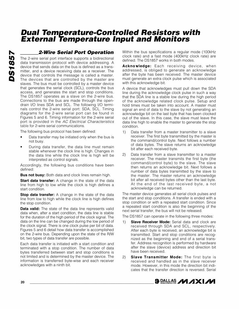
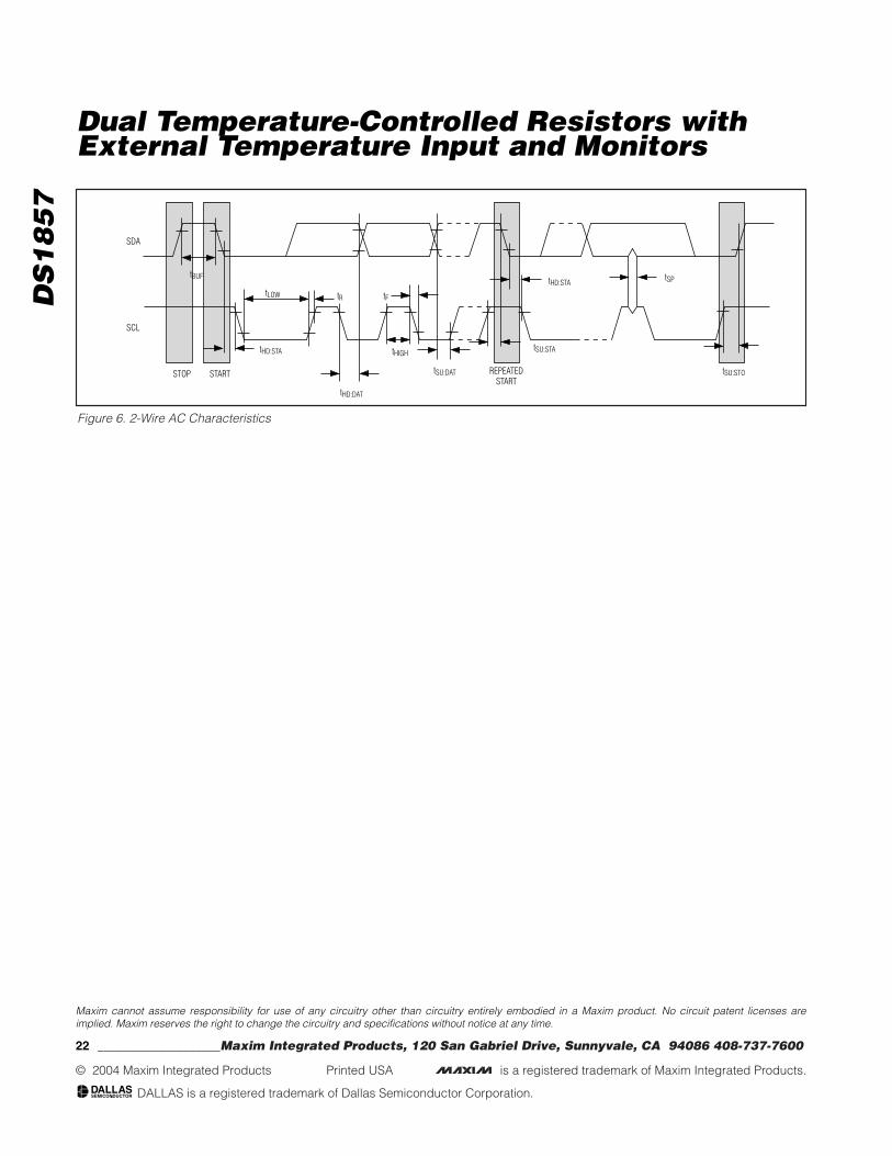
2-Wire Serial Port OperationThe 2-wire serial port interface supports a bidirectionaldata transmission protocol with device addressing. Adevice that sends data on the bus is defined as a trans-mitter, and a device receiving data as a receiver. Thedevice that controls the message is called a master.The devices that are controlled by the master areslaves. The bus must be controlled by a master devicethat generates the serial clock (SCL), controls the busaccess, and generates the start and stop conditions.The DS1857 operates as a slave on the 2-wire bus.Connections to the bus are made through the open-drain I/O lines SDA and SCL. The following I/O termi-nals control the 2-wire serial port: SDA, SCL. Timingdiagrams for the 2-wire serial port can be found inFigures 5 and 6. Timing information for the 2-wire serialport is provided in the AC Electrical Characteristicstable for 2-wire serial communications.
The following bus protocol has been defined:
• Data transfer may be initiated only when the bus isnot busy.
• During data transfer, the data line must remainstable whenever the clock line is high. Changes inthe data line while the clock line is high will beinterpreted as control signals.
Accordingly, the following bus conditions have beendefined:
Bus not busy: Both data and clock lines remain high.
Start data transfer: A change in the state of the dataline from high to low while the clock is high defines astart condition.
Stop data transfer: A change in the state of the dataline from low to high while the clock line is high definesthe stop condition.
Data valid: The state of the data line represents validdata when, after a start condition, the data line is stablefor the duration of the high period of the clock signal. Thedata on the line can be changed during the low period ofthe clock signal. There is one clock pulse per bit of data.Figures 5 and 6 detail how data transfer is accomplishedon the 2-wire bus. Depending upon the state of the R/Wbit, two types of data transfer are possible.
Each data transfer is initiated with a start condition andterminated with a stop condition. The number of databytes transferred between start and stop conditions isnot limited and is determined by the master device. Theinformation is transferred byte-wise and each receiveracknowledges with a ninth bit.
Within the bus specifications a regular mode (100kHzclock rate) and a fast mode (400kHz clock rate) aredefined. The DS1857 works in both modes.
Acknowledge: Each receiving device, whenaddressed, is obliged to generate an acknowledgeafter the byte has been received. The master devicemust generate an extra clock pulse which is associatedwith this acknowledge bit.
A device that acknowledges must pull down the SDAline during the acknowledge clock pulse in such a waythat the SDA line is a stable low during the high periodof the acknowledge related clock pulse. Setup andhold times must be taken into account. A master mustsignal an end of data to the slave by not generating anacknowledge bit on the last byte that has been clockedout of the slave. In this case, the slave must leave thedata line high to enable the master to generate the stopcondition.
1) Data transfer from a master transmitter to a slavereceiver. The first byte transmitted by the master isthe command/control byte. Next follows a numberof data bytes. The slave returns an acknowledgebit after each received byte.
2) Data transfer from a slave transmitter to a masterreceiver. The master transmits the first byte (thecommand/control byte) to the slave. The slavethen returns an acknowledge bit. Next follows anumber of data bytes transmitted by the slave tothe master. The master returns an acknowledgebit after all received bytes other than the last byte.At the end of the last received byte, a notacknowledge can be returned.
The master device generates all serial clock pulses andthe start and stop conditions. A transfer is ended with astop condition or with a repeated start condition. Sincea repeated start condition is also the beginning of thenext serial transfer, the bus will not be released.
The DS1857 can operate in the following three modes:
1) Slave Receiver Mode: Serial data and clock arereceived through SDA and SCL, respectively.After each byte is received, an acknowledge bit istransmitted. Start and stop conditions are recog-nized as the beginning and end of a serial trans-fer. Address recognition is performed by hardwareafter the slave (device) address and direction bithave been received.
2) Slave Transmitter Mode: The first byte isreceived and handled as in the slave receivermode. However, in this mode the direction bit indi-cates that the transfer direction is reversed. Serial
DS
18
57
Dual Temperature-Controlled Resistors withExternal Temperature Input and Monitors
____________________________________________________________________ 21
data is transmitted on SDA by the DS1857, whilethe serial clock is input on SCL. Start and stopconditions are recognized as the beginning andend of a serial transfer.
3) Slave Address: Command/control byte is the firstbyte received following the start condition from themaster device. The command/control byte con-sists of a 4-bit control code. For the DS1857, thisis set as 1010 binary for read/write operations. Thenext three bits of the command/control byte arethe device select bits or device address. They areused by the master device to select which of eightpossible devices on the bus is to be accessed.When reading or writing the DS1857, the device-select bits must match one of two valid deviceaddresses 00h, or the address registered in Table01 location 8Ch. The last bit of the command/con-trol byte (R/W) defines the operation to be per-formed. When set to a ‘1’ a read operation isselected, and when set to a ‘0’ a write operation isselected. The slave address can be set by theEEPROM.
Following the start condition, the DS1857 monitors theSDA bus checking the device type identifier beingtransmitted. Upon receiving the 1010 control code, the
appropriate device address bits, and the read/write bit,the slave device outputs an acknowledge signal on theSDA line.
Chip TopologyTRANSISTOR COUNT: 44149
SUBSTRATE CONNECTED TO GROUND.
STOPCONDITION
OR REPEATEDSTART
CONDITION
REPEATED IF MORE BYTESARE TRANSFERRED
ACKSTART
CONDITION
ACK
ACKNOWLEDGEMENTSIGNAL FROM RECEIVER
ACKNOWLEDGEMENTSIGNAL FROM RECEIVER
SLAVE ADDRESS
MSB
SCL
SDA
R/WDIRECTION
BIT
1 2 6 7 8 9 1 2 8 93–7
Figure 5. 2-Wire Data Transfer Protocol
DS
18
57
Dual Temperature-Controlled Resistors withExternal Temperature Input and Monitors
Maxim cannot assume responsibility for use of any circuitry other than circuitry entirely embodied in a Maxim product. No circuit patent licenses areimplied. Maxim reserves the right to change the circuitry and specifications without notice at any time.
22 ____________________Maxim Integrated Products, 120 San Gabriel Drive, Sunnyvale, CA 94086 408-737-7600
© 2004 Maxim Integrated Products Printed USA is a registered trademark of Maxim Integrated Products.
DALLAS is a registered trademark of Dallas Semiconductor Corporation.
SDA
SCL
tHD:STA
tLOW
tHIGH
tR tF
tBUF
tHD:DAT
tSU:DAT REPEATEDSTART
tSU:STA
tHD:STA
tSU:STO
tSP
STOP START
Figure 6. 2-Wire AC Characteristics