Embed Size (px)
Citation preview
DYNAMIC CHARACTERISTICS OF THYRISTOR
Thyristor Turn-ON Characteristics
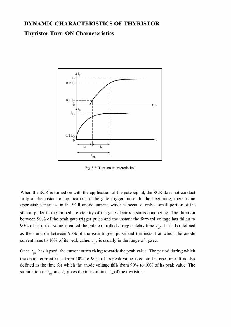
Fig.3.7: Turn-on characteristics
When the SCR is turned on with the application of the gate signal, the SCR does not conduct fully at the instant of application of the gate trigger pulse. In the beginning, there is no appreciable increase in the SCR anode current, which is because, only a small portion of the
silicon pellet in the immediate vicinity of the gate electrode starts conducting. The duration between 90% of the peak gate trigger pulse and the instant the forward voltage has fallen to 90% of its initial value is called the gate controlled / trigger delay time gdt . It is also defined
as the duration between 90% of the gate trigger pulse and the instant at which the anode current rises to 10% of its peak value. gdt is usually in the range of 1 sec.
Once gdt has lapsed, the current starts rising towards the peak value. The period during which
the anode current rises from 10% to 90% of its peak value is called the rise time. It is also defined as the time for which the anode voltage falls from 90% to 10% of its peak value. The summation of gdt and rt gives the turn on time ont of the thyristor.
Thyristor Turn OFF Characteristics
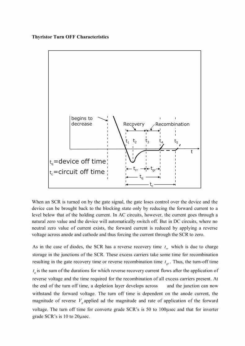
When an SCR is turned on by the gate signal, the gate loses control over the device and the device can be brought back to the blocking state only by reducing the forward current to a level below that of the holding current. In AC circuits, however, the current goes through a natural zero value and the device will automatically switch off. But in DC circuits, where no neutral zero value of current exists, the forward current is reduced by applying a reverse voltage across anode and cathode and thus forcing the current through the SCR to zero.
Anode current
begins todecrease
tCtq
t
t
Commutationdidt
Recovery Recombination
t1 t2 t3 t4 t5
trr tgr
tq
tc
VAK
IA
tq=device off time
tc=circuit off time
As in the case of diodes, the SCR has a reverse recovery time rrt which is due to charge storage in the junctions of the SCR. These excess carriers take some time for recombination resulting in the gate recovery time or reverse recombination time grt . Thus, the turn-off time
qt is the sum of the durations for which reverse recovery current flows after the application of
reverse voltage and the time required for the recombination of all excess carriers present. At the end of the turn off time, a depletion layer develops across and the junction can now withstand the forward voltage. The turn off time is dependent on the anode current, the magnitude of reverse gV applied ad the magnitude and rate of application of the forward
voltage. The turn off time for converte grade SCR’s is 50 to 100 sec and that for inverter grade SCR’s is 10 to 20 sec.
qt
To ensure that SCR has successfully turned off , it is required that the circuit off time ct be
greater than SCR turn off time qt .
Thyristor Turn ON
Thermal Turn on: If the temperature of the thyristor is high, there will be an increase in charge carriers which would increase the leakage current. This would cause an increase in 1 & 2 and the thyristor may turn on. This type of turn on many cause thermal run away and is usually avoided.
Light: If light be allowed to fall on the junctions of a thyristor, charge carrier concentration would increase which may turn on the SCR.
LASCR: Light activated SCRs are turned on by allowing light to strike the silicon wafer.
High Voltage Triggering: This is triggering without application of gate voltage with only application of a large voltage across the anode-cathode such that it is greater than the forward breakdown voltage BOV . This type of turn on is destructive and should be avoided.
Gate Triggering: Gate triggering is the method practically employed to turn-on the thyristor. Gate triggering will be discussed in detail later.
dvdt
Triggering: Under transient conditions, the capacitances of the p-n junction will
influence the characteristics of a thyristor. If the thyristor is in the blocking state, a rapidly rising voltage applied across the device would cause a high current to flow through the device resulting in turn-on. If
2ji is the current throught the junction 2j and
2jC is the junction capacitance and
2jV is the voltage across 2j , then
2 2
2 22 2
22 j J jj j j j
C dV dCdq di C V Vdt dt dt dt
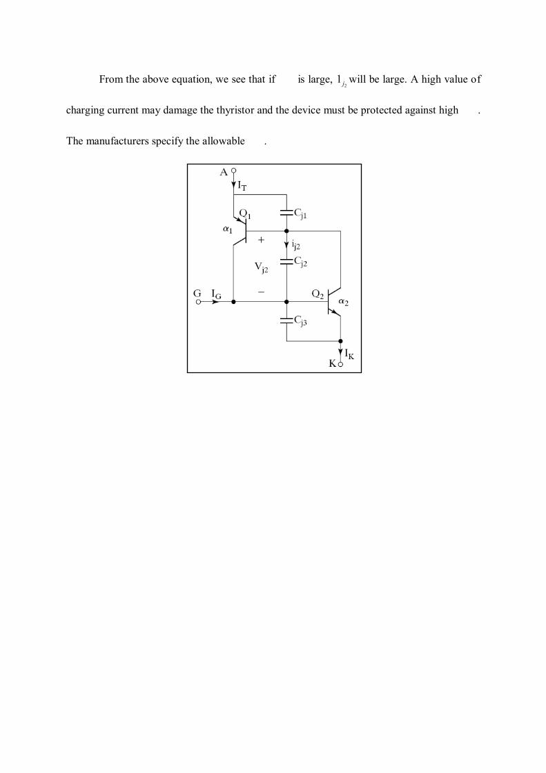
From the above equation, we see that if
dvdt
is large, 2
1 j will be large. A high value of
charging current may damage the thyristor and the device must be protected against high
dvdt
.
The manufacturers specify the allowable
dvdt
.