Embed Size (px)
Citation preview
sensors
Article
E-Skin Bimodal Sensors for Robotics and ProsthesisUsing PDMS Molds Engraved by Laser †
Andreia dos Santos , Nuno Pinela, Pedro Alves, Rodrigo Santos, Ricardo Farinha ,Elvira Fortunato, Rodrigo Martins, Hugo Águas and Rui Igreja *
CENIMAT|i3N, Departamento de Ciência dos Materiais, Faculdade de Ciências e Tecnologia, UniversidadeNova de Lisboa, Campus de Caparica, 2829-516 Caparica, Portugal; [email protected] (A.d.S.);[email protected] (N.P.); [email protected] (P.A.); [email protected] (R.S.);[email protected] (R.F.); [email protected] (E.F.); [email protected] (R.M.); [email protected] (H.Á.)* Correspondence: [email protected]; Tel.: +351-21-294-8562† This paper is an extended version of our paper published in: Santos, A.D.; Pinela, N.; Alves, P.; Santos, R.;
Fortunato, E.; Martins, R.; Águas, H.; Igreja, R. E-Skin Pressure Sensors Made by Laser Engraved PDMSMolds. In Proceedings of the Eurosensors 2018 Conference, Graz, Austria, 9–12 September 2018.
Received: 28 December 2018; Accepted: 18 February 2019; Published: 21 February 2019
Abstract: Electronic skin (e-skin) is pursued as a key component in robotics and prosthesis to conferthem sensing properties that mimic human skin. For pressure monitoring, a great emphasis onpiezoresistive sensors was registered due to the simplicity of sensor design and readout mechanism.For higher sensitivity, films composing these sensors may be micro-structured, usually by expensivephotolithography techniques or low-cost and low-customizable molds. Sensors commonly presentdifferent sensitivities in different pressure ranges, which should be avoided in robotics and prosthesisapplications. The combination of pressure sensing and temperature is also relevant for the field andhas room for improvement. This work proposes an alternative approach for film micro-structurationbased on the production of highly customizable and low-cost molds through laser engraving.These bimodal e-skin piezoresistive and temperature sensors could achieve a stable sensitivityof −6.4 × 10⁻³ kPa−1 from 1.6 kPa to 100 kPa, with a very robust and reproducible performance over27,500 cycles of objects grasping and releasing and an exceptionally high temperature coefficient ofresistance (TCR) of 8.3%/C. These results point toward the versatility and high benefit/cost ratioof the laser engraving technique to produce sensors with a suitable performance for robotics andfunctional prosthesis.
Keywords: electronic skin; pressure; piezoresistivity; micro-structuration; temperature; laserengraving; molds; bimodal sensors; robotics; prosthesis
1. Introduction
Nature is an endless source of inspiration for the human being. Almost everything that surroundsus may be looked at with a different perspective, seeking new ideas to improve our lives. Human skinis often underrated due to the simplistic way people look at it: an organ that protects other organsthat are considered to be vital for our existence. However, if one starts considering all the functionsattributed to skin, its complexity immediately acquires a dimension previously unrecognized; skin notonly protects us from pathogenic agents and other environmental aggressions like ultraviolet (UV)light, but also plays an important role for the homeostasis of the human body, being also equippedwith several biological sensors to detect temperature, humidity, pain, mechanical forces, textures,and so on [1,2]. The creation of a human skin surrogate with some or all the mentioned sensingproperties, as well as flexibility and stretchability, the so-called electronic skin (e-skin) [1], is pursued
Sensors 2019, 19, 899; doi:10.3390/s19040899 www.mdpi.com/journal/sensors
Sensors 2019, 19, 899 2 of 15
by the scientific community aiming for its application in a variety of fields, from robots [3–5] to healthmonitoring [6–15] and functional prosthesis [16–18].
Sensors dedicated to pressure sensing may rely on some distinct effects to accurately transducea pressure signal into an electrical signal, namely piezoresistivity [19–27], capacitance [6,17,28–30],piezoelectricity [8,15,31,32], and triboelectricity [33–36]. Given that it is quite simple to both designand read the output signal of a sensor that plays on piezoresistivity, this effect fueled a great levelof research in the field, where a pressure variation is transduced into a change in resistance, mostlyderived from changes in the geometry of the sensing element, the resistivity of a composite dueto changes in separation between particles, or the contact resistance [1]. For the latter, the creationof micro-structured domains in films that compose the sensors increases the contact area betweenfilms, thereby increasing the ROFF/RON ratio [9,23,27] and, consequently, translating into an improvedsensor sensitivity.
The majority of sensors so far reported typically exhibit two different sensitivity values dependingon the applied pressure: a higher value for low pressures and a significantly lower value for higherpressures [6,9,20,22–26,28,30,34,37–41]. If such sensors are to be used in the wrist for the detection ofthe blood pressure wave, the requirement is for these to show a high sensitivity below 400 Pa [19].In the case of functional prosthesis and robotics, the need is different; sensors should be able toaccurately detect pressure stimuli in a range that is associated to human common interactions withthe surroundings, from less than 10 kPa for gentle touch to 100 kPa for object manipulation [20,28];thus, a constant sensitivity in such a pressure range would be preferable. Moreover, the two mostexplored approaches for the sensor micro-structuration are based on the use of either expensiveand time-consuming photolithography techniques [6,9–12,19,23,26–28,33–35,37] or low-cost but alsolow-customizable techniques consisting of the use of everyday objects as molds [22,36,42]. Thereis, therefore, a need for the development of a low-cost e-skin pressure sensor for which productionis based on simple and highly customizable techniques. Such customization is crucial to tailor theperformance of the sensors to each application, either showing a high sensitivity in a low-pressurerange for health applications, or a constant sensitivity in a wide pressure range that is meaningful forprosthesis and robotics applications.
In order to sense both pressure and temperature, researchers worked either on sensors able tosimultaneously detect both stimuli or on the integration of multiple sensors. While the first optionmay imply complex data analysis to distinguish the contribution of each stimulus to the sensor’soutput [43,44], the second requires special attention to prevent or minimize sensors’ cross-sensitivityand may lead to bulky sensors [16,45], which still leaves room for further research and improvementof current e-skin sensors to achieve more functional prosthesis and robots.
This group recently introduced a micro-structuration technique for polymeric films basedon the easy and fast production of highly customizable acrylic molds through a laser engravingequipment [46]. The resultant sensors, with micro-cones as their micro-structuration, exhibited a highsensitivity of −2.5 kPa−1 below 160 Pa, a value that decreases for higher pressures. Herein, otherdesigns for the molds were explored in order to tailor the sensitivity of the sensors and extend thecorrespondent pressure range from less than 10 kPa to 100 kPa to make them suitable for prosthesis androbotics applications. Instead of using acrylic, hard polydimethylsiloxane (h-PDMS) was explored asthe material of the molds. With circular cavities engraved in the molds, standard PDMS (s-PDMS) filmswith semi-sphere like structures were patterned by soft-lithography and used in e-skin piezoresistivesensors that could achieve a sensitivity as high as −6.4 × 10⁻³ kPa−1 between 1.6 kPa and 100 kPa,a pressure range that is relevant in the field of robotics and prosthesis. These sensors could alsoachieve a temperature coefficient of resistance (TCR) of 8.3%/C. Poly(methyl methacrylate) (PMMA)was studied as an adhesion layer between carbon coating (the active material of the sensor) ands-PDMS. Sensors that had this layer presented a more stable performance and faster relaxation timesuntil a minimum of 28 ms, which made them better than sensors without PMMA. Fatigue testswere conducted in these sensors by placing them in a robotic arm and evaluating their performance
Sensors 2019, 19, 899 3 of 15
over 27,500 cycles of grasping and releasing of an object, proving their relevance for this type ofapplication. Despite not exploring innovative shapes for the micro-structures nor a new design for thepressure and temperature sensors, this work, which is an extended version of a conference paper [47],ultimately shows the versatility of laser-engraved molds for the production of sensors suitable for aplethora of applications, where one only needs to change the design features of the sensor to have asubstantial impact on its performance. Furthermore, although the micro-structures achieved throughthis technique are not as homogeneous and regular as those produced through photolithographytechniques, they were proven to be very functional, which highlights the high benefit/cost ratio ofusing laser engraving for the micro-structuration of films for e-skin sensors.
2. Materials and Methods
2.1. Chemicals and Materials
PDMS elastomer and curing agent (Sylgard 184) were purchased from Dow Corning (Midland,MI, USA). PMMA (molecular weight (MW) approximately 120,000) and trichloro(1H,1H,2H,2H-perfluorooctyl)silane (97%) were purchased from Aldrich (St. Louis, MO, USA). Toluene (99.99%) waspurchased from Fisher Scientific (Loughborough, UK). Highly conductive water-based carbon coating(PE-C-808) and water-based silver conductive ink (PE-WB-1078) were purchased from ConductiveCompounds (Hudson, NH, USA).
2.2. Fabrication and Laser Engraving of h-PDMS Molds
Patterns to be engraved in the molds were designed in Illustrator® (2015.0.0) and exported ascomputer-aided design (CAD) files. These patterns consisted of a repetition of circles with a diameterof 100 µm or 200 µm and a pitch of 150 µm or 200 µm over an area of 2 cm × 2 cm.
Hard PDMS molds were fabricated by mixing PDMS curing agent with PDMS elastomer in a 1:5w/w ratio. The mixture was then degassed in vacuum for 30 min, poured into a Petri dish, and curedfor 1 hour at 70 C. The h-PDMS molds (5 mm thick) were micro-structured using a laser engravingmachine (VLS3.50, 50 W, Universal Laser System, USA) with a CO2 laser beam, a lens focus lengthof 2.0 in, and a focal spot of 127 µm in diameter, according to the imported CAD file, as shown inFigure 1a. The engraving was performed with a laser speed of 0.254 m/s and a laser power of 2.5 W,7.5 W, 12.5 W, or 25 W.
The molds were afterward cleaned in an ultrasonic bath for 10 min in isopropanol alcohol, rinsedin MiliQ water, and dried with compressed air. Then, the molds were placed in a desiccator for 30 min,together with 1 drop of trichloro(1H,1H,2H,2H-perfluorooctyl)silane, to be covered by a hydrophobiclayer and facilitate the peeling of s-PDMS films.
2.3. Fabrication of E-Skin Sensors
Standard PDMS was prepared in a ratio of 1:10 w/w of curing agent to elastomer and wassubsequently degassed in vacuum for 30 min. The mixture was then spin-coated at 250 rpm for 90 sonto each engraved h-PDMS mold (Figure 1b), followed by another degassing process and curingat 85 C for 30 min in an Infrared IC Heater (T-962 Eco-Worthy). Posteriorly, the micro-structureds-PDMS films were easily peeled off, as shown in Figure 1c, and submitted to an O2 plasma treatment(37.5 W for 1 min with an O2 pressure of 0.3 mbar) before spin-coating PMMA (10 wt.% in toluene) at1000 rpm for 1 min (Figure 1d). Thermal curing of PMMA films occurred in vacuum for 1 h at 140 C.
The PMMA-coated s-PDMS films underwent another O2 plasma treatment before spin-coatinghighly conductive water-based carbon coating (PE-C-808) at 1000 rpm for 20 s (Figure 1e). The carboncoating was cured for 30 min at 85 C to finalize the treatment of each film, as shown in Figure 1f.After cutting the s-PDMS films (3 cm × 2 cm), pairs of films with the same pattern were sandwichedand sealed with s-PDMS. Lateral transducer electrodes were created by depositing lines (1 cm width)of 50 wt.% in water of water-based silver conductive ink (PE-WB-1078) on the edges of each film. The
Sensors 2019, 19, 899 4 of 15
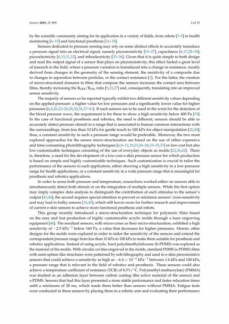
curing of this ink was done for 120 s at 145 C. A scheme of a final e-skin piezoresistive sensor is shownin Figure 1g, with the inset highlighting the semi-spheres and all the layers that compose them.Sensors 2019, 19, x FOR PEER REVIEW 4 of 16
Figure 1. Fabrication process of an e-skin piezoresistive sensor. (a) Laser engraving cavities on a hard polydimethylsiloxane (h-PDMS) mold. (b) Standard PDMS (s-PDMS) spin-coating on the engraved mold. (c) Peeling off the flexible s-PDMS film from the mold. (d) Poly(methyl methacrylate) (PMMA) spin-coating on the s-PDMS film. (e) Carbon coating spin-coating on the previous film. (f) Final micro-structured film after curing of carbon coating. (g) Final device with a silver-ink stripe on the smooth edge of each film. None of the steps are to scale.
2.4. Morphological Characterization of Micro-Structured s-PDMS Films
Micro-structured h-PDMS molds and s-PDMS films were coated with a gold/palladium (Au/Pd) layer of 15 nm and observed with a tabletop scanning electron microscope (SEM) (Hitachi TM3030Plus) in standard observation mode at 15 kV. Measurements of the micro-features were performed using the software ImageJ (1.49b). A profilometer (Ambios XP-Plus 200 Stylus) using a tracking force of 1 mg and a speed of 0.10 mm∙s−1 was used to estimate the roughness of PDMS films, performing five to 10 measurements of each sample. A contact-angle equipment (Dataphysics OCA15plus) was used to measure the contact angle in PDMS films before and after the oxygen plasma treatment referred to in Section 2.3.
2.5. Electrical Characterization of Films and Sensors
A Keithley 617 Programmable Electrometer was employed for the acquisition of current–voltage (I–V) curves of the films and sensors, with a voltage sweep from −2 V to 2 V, in steps of 0.5 V. To test the sensors response to changes in pressure, several weights were loaded on the sensors to apply pressures from 15 Pa to 100 kPa, at a constant voltage of 5 V to 10 V. To estimate the relaxation time, a small magnet (~184 Pa) was loaded and unloaded on top of the sensors. The temperature response of the sensors was evaluated by applying a temperature in increments of 1 °C from 25 °C to 45 °C while monitoring the nominal resistance change. Pressure stability tests were conducted after mounting sensors in a robotic arm controlled by a servomotor. The sensors monitored the pressure exerted by the robotic arm during the grasping of a volumetric flask, which was performed 27,500 times. Except for the temperature response evaluation, all the electrical characterization of the sensors was performed at room temperature. The impact of humidity on the performance of the sensors was not evaluated, although all the characterization was performed at a constant humidity of 60%, and the sensors could be completely laterally sealed to avoid the contact of the carbon coating with atmospheric humidity.
3. Results and Discussion
Figure 1. Fabrication process of an e-skin piezoresistive sensor. (a) Laser engraving cavities on a hardpolydimethylsiloxane (h-PDMS) mold. (b) Standard PDMS (s-PDMS) spin-coating on the engravedmold. (c) Peeling off the flexible s-PDMS film from the mold. (d) Poly(methyl methacrylate) (PMMA)spin-coating on the s-PDMS film. (e) Carbon coating spin-coating on the previous film. (f) Finalmicro-structured film after curing of carbon coating. (g) Final device with a silver-ink stripe on thesmooth edge of each film. None of the steps are to scale.
2.4. Morphological Characterization of Micro-Structured s-PDMS Films
Micro-structured h-PDMS molds and s-PDMS films were coated with a gold/palladium (Au/Pd)layer of 15 nm and observed with a tabletop scanning electron microscope (SEM) (Hitachi TM3030Plus)in standard observation mode at 15 kV. Measurements of the micro-features were performed using thesoftware ImageJ (1.49b). A profilometer (Ambios XP-Plus 200 Stylus) using a tracking force of 1 mgand a speed of 0.10 mm·s−1 was used to estimate the roughness of PDMS films, performing five to10 measurements of each sample. A contact-angle equipment (Dataphysics OCA15plus) was used tomeasure the contact angle in PDMS films before and after the oxygen plasma treatment referred to inSection 2.3.
2.5. Electrical Characterization of Films and Sensors
A Keithley 617 Programmable Electrometer was employed for the acquisition of current–voltage(I–V) curves of the films and sensors, with a voltage sweep from −2 V to 2 V, in steps of 0.5 V. To testthe sensors response to changes in pressure, several weights were loaded on the sensors to applypressures from 15 Pa to 100 kPa, at a constant voltage of 5 V to 10 V. To estimate the relaxation time, asmall magnet (~184 Pa) was loaded and unloaded on top of the sensors. The temperature response ofthe sensors was evaluated by applying a temperature in increments of 1 C from 25 C to 45 C whilemonitoring the nominal resistance change. Pressure stability tests were conducted after mountingsensors in a robotic arm controlled by a servomotor. The sensors monitored the pressure exerted by therobotic arm during the grasping of a volumetric flask, which was performed 27,500 times. Except forthe temperature response evaluation, all the electrical characterization of the sensors was performedat room temperature. The impact of humidity on the performance of the sensors was not evaluated,
Sensors 2019, 19, 899 5 of 15
although all the characterization was performed at a constant humidity of 60%, and the sensors couldbe completely laterally sealed to avoid the contact of the carbon coating with atmospheric humidity.
3. Results and Discussion
3.1. Hard PDMS Molds Patterning
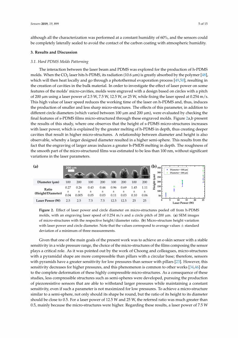
The interaction between the laser beam and PDMS was explored for the production of h-PDMSmolds. When the CO2 laser hits h-PDMS, its radiation (10.6 µm) is greatly absorbed by the polymer [48],which will then heat locally and go through a photothermal evaporation process [49,50], resulting inthe creation of cavities in the bulk material. In order to investigate the effect of laser power on somefeatures of the molds’ micro-cavities, molds were engraved with a design based on circles with a pitchof 200 µm using a laser power of 2.5 W, 7.5 W, 12.5 W, or 25 W, while fixing the laser speed at 0.254 m/s.This high value of laser speed reduces the working time of the laser on h-PDMS and, thus, inducesthe production of smaller and less sharp micro-structures. The effects of this parameter, in addition todifferent circle diameters (which varied between 100 µm and 200 µm), were evaluated by checking thefinal features of s-PDMS films micro-structured through these engraved molds. Figure 2a,b presentthe results of this study, where one observes that the height of s-PDMS micro-structures increaseswith laser power, which is explained by the greater melting of h-PDMS in depth, thus creating deepercavities that result in higher micro-structures. A relationship between diameter and height is alsoobservable, whereby a larger designed diameter resulted in a higher semi-sphere. This results from thefact that the engraving of larger areas induces a greater h-PMDS melting in depth. The roughness ofthe smooth part of the micro-structured films was estimated to be less than 100 nm, without significantvariations in the laser parameters.
Sensors 2019, 19, x FOR PEER REVIEW 5 of 16
3.1. Hard PDMS Molds Patterning
The interaction between the laser beam and PDMS was explored for the production of h-PDMS molds. When the CO2 laser hits h-PDMS, its radiation (10.6 µm) is greatly absorbed by the polymer [48], which will then heat locally and go through a photothermal evaporation process [49,50], resulting in the creation of cavities in the bulk material. In order to investigate the effect of laser power on some features of the molds’ micro-cavities, molds were engraved with a design based on circles with a pitch of 200 µm using a laser power of 2.5 W, 7.5 W, 12.5 W, or 25 W, while fixing the laser speed at 0.254 m/s. This high value of laser speed reduces the working time of the laser on h-PDMS and, thus, induces the production of smaller and less sharp micro-structures. The effects of this parameter, in addition to different circle diameters (which varied between 100 µm and 200 µm), were evaluated by checking the final features of s-PDMS films micro-structured through these engraved molds. Figure 2a,b present the results of this study, where one observes that the height of s-PDMS micro-structures increases with laser power, which is explained by the greater melting of h-PDMS in depth, thus creating deeper cavities that result in higher micro-structures. A relationship between diameter and height is also observable, whereby a larger designed diameter resulted in a higher semi-sphere. This results from the fact that the engraving of larger areas induces a greater h-PMDS melting in depth. The roughness of the smooth part of the micro-structured films was estimated to be less than 100 nm, without significant variations in the laser parameters.
Given that one of the main goals of the present work was to achieve an e-skin sensor with a stable sensitivity in a wide pressure range, the choice of the micro-structures of the films composing the sensor plays a critical role. As it was pointed out by the work of Choong and colleagues, micro-structures with a pyramidal shape are more compressible than pillars with a circular base; therefore, sensors with pyramids have a greater sensitivity for low pressures than sensor with pillars [23]. However, this sensitivity decreases for higher pressures, and this phenomenon is common to other works [34,46] due to the complete deformation of these highly compressible micro-structures. As a consequence of these studies, less compressible structures such as semi-spheres were developed, pursuing the production of piezoresistive sensors that are able to withstand larger pressures while maintaining a constant sensitivity, even if such a parameter is not maximized for low pressures. To achieve a micro-structure similar to a semi-sphere, not only should its shape be round, but the ratio of its height to its diameter should be close to 0.5. For a laser power of 12.5 W and 25 W, the referred ratio was much greater than 0.5, mainly because the micro-structures were higher. Regarding these results, a laser power of 7.5 W seems to be more appropriate to produce semi-sphere like structures, given that the height/diameter ratio for this condition was closer to 0.5.
Figure 2. Effect of laser power and circle diameter on micro-structures peeled off from h-PDMS molds, with an engraving laser speed of 0.254 m/s and a circle pitch of 200 µm. (a) SEM images of micro-structures with the respective height/diameter ratio. (b) Micro-structure height variation with laser power and circle diameter. Note that the values correspond to average values ± standard deviation of a minimum of three measurements.
Micro-structures resultant from two similar designs were used to compare the theoretical diameter and pitch with the real measurements of these features, as well as to compare the laser engraving resolution over vertical and horizontal directions. Such micro-structures were produced after engraving molds with circles with a theoretical diameter of 100 µm or 200 µm and a pitch of 150
0 5 10 15 20 25
50
100
150
200
250
300
350Diameter = 100 μmDiameter = 200 μm
Hei
ght (
μm)
Laser Power (W)
Diameter (µm) 100 200 100 200 100 200 100 200
Ratio(Height/Diameter)
0.27±
0.04
0.26±
0.005
0.43±
0.05
0.44±
0.03
0.96±
0.11
0.69±
0.03
1.45±
0.10
1.11±
0.06Laser Power (W) 2.5 2.5 7.5 7.5 12.5 12.5 25 25
200 μm(a) (b)
Figure 2. Effect of laser power and circle diameter on micro-structures peeled off from h-PDMSmolds, with an engraving laser speed of 0.254 m/s and a circle pitch of 200 µm. (a) SEM imagesof micro-structures with the respective height/diameter ratio. (b) Micro-structure height variationwith laser power and circle diameter. Note that the values correspond to average values ± standarddeviation of a minimum of three measurements.
Given that one of the main goals of the present work was to achieve an e-skin sensor with a stablesensitivity in a wide pressure range, the choice of the micro-structures of the films composing the sensorplays a critical role. As it was pointed out by the work of Choong and colleagues, micro-structureswith a pyramidal shape are more compressible than pillars with a circular base; therefore, sensorswith pyramids have a greater sensitivity for low pressures than sensor with pillars [23]. However, thissensitivity decreases for higher pressures, and this phenomenon is common to other works [34,46] dueto the complete deformation of these highly compressible micro-structures. As a consequence of thesestudies, less compressible structures such as semi-spheres were developed, pursuing the productionof piezoresistive sensors that are able to withstand larger pressures while maintaining a constantsensitivity, even if such a parameter is not maximized for low pressures. To achieve a micro-structuresimilar to a semi-sphere, not only should its shape be round, but the ratio of its height to its diametershould be close to 0.5. For a laser power of 12.5 W and 25 W, the referred ratio was much greater than0.5, mainly because the micro-structures were higher. Regarding these results, a laser power of 7.5 W
Sensors 2019, 19, 899 6 of 15
seems to be more appropriate to produce semi-sphere like structures, given that the height/diameterratio for this condition was closer to 0.5.
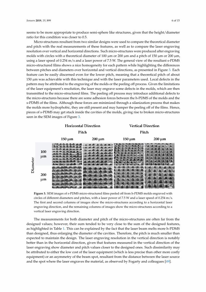
Micro-structures resultant from two similar designs were used to compare the theoretical diameterand pitch with the real measurements of these features, as well as to compare the laser engravingresolution over vertical and horizontal directions. Such micro-structures were produced after engravingmolds with circles with a theoretical diameter of 100 µm or 200 µm and a pitch of 150 µm or 200 µm,using a laser speed of 0.254 m/s and a laser power of 7.5 W. The general view of the resultant s-PDMSmicro-structured films shows a nice homogeneity for each pattern while highlighting the differencesbetween pitches and diameters over horizontal and vertical directions, as presented in Figure 3. Eachfeature can be easily discerned even for the lower pitch, meaning that a theoretical pitch of about150 µm was achievable with this technique and with the laser parameters used. Local defects in thepattern may be attributed to the engraving of the molds or the peeling off process. Given the limitationsof the laser equipment’s resolution, the laser may engrave some defects in the molds, which are thentransmitted to the micro-structured films. The peeling off process may introduce additional defects tothe micro-structures because there are some adhesion forces between the h-PDMS of the molds and thes-PDMS of the films. Although these forces are minimized through a silanization process that makesthe molds more hydrophobic, they are still present and may hamper the peeling off of the films. Hence,pieces of s-PDMS may get stuck inside the cavities of the molds, giving rise to broken micro-structuresseen in the SEM images of Figure 3.
Sensors 2019, 19, x FOR PEER REVIEW 6 of 16
µm or 200 µm, using a laser speed of 0.254 m/s and a laser power of 7.5 W. The general view of the resultant s-PDMS micro-structured films shows a nice homogeneity for each pattern while highlighting the differences between pitches and diameters over horizontal and vertical directions, as presented in Figure 3. Each feature can be easily discerned even for the lower pitch, meaning that a theoretical pitch of about 150 µm was achievable with this technique and with the laser parameters used. Local defects in the pattern may be attributed to the engraving of the molds or the peeling off process. Given the limitations of the laser equipment’s resolution, the laser may engrave some defects in the molds, which are then transmitted to the micro-structured films. The peeling off process may introduce additional defects to the micro-structures because there are some adhesion forces between the h-PDMS of the molds and the s-PDMS of the films. Although these forces are minimized through a silanization process that makes the molds more hydrophobic, they are still present and may hamper the peeling off of the films. Hence, pieces of s-PDMS may get stuck inside the cavities of the molds, giving rise to broken micro-structures seen in the SEM images of Figure 3.
Figure 3. SEM images of s-PDMS micro-structured films peeled off from h-PDMS molds engraved with circles of different diameters and pitches, with a laser power of 7.5 W and a laser speed of 0.254 m/s. The first and second columns of images show the micro-structures according to a horizontal laser engraving direction, and the remaining columns of images show the micro-structures according to a vertical laser engraving direction.
The measurements for both diameter and pitch of the micro-structures are often far from the designed values; however, their sum tended to be very close to the sum of the designed features, as highlighted in Table 1. This can be explained by the fact that the laser beam melts more h-PDMS than designed, thus enlarging the diameter of the cavities. Therefore, the pitch is much smaller than expected to maintain the design. The laser engraving resolution in the vertical direction is notably better than in the horizontal direction, given that features measured in the vertical direction of the laser engraving show diameter and pitch values closer to the designed ones. Such dissimilarity may be attributed to either the low cost of the laser equipment (which is less precise than other more costly equipment) or an asymmetry of the beam spot, resultant from the distance between the laser source and the spot where the laser engraves the material, as observed by Fogarty and colleagues [49].
Figure 3. SEM images of s-PDMS micro-structured films peeled off from h-PDMS molds engraved withcircles of different diameters and pitches, with a laser power of 7.5 W and a laser speed of 0.254 m/s.The first and second columns of images show the micro-structures according to a horizontal laserengraving direction, and the remaining columns of images show the micro-structures according to avertical laser engraving direction.
The measurements for both diameter and pitch of the micro-structures are often far from thedesigned values; however, their sum tended to be very close to the sum of the designed features,as highlighted in Table 1. This can be explained by the fact that the laser beam melts more h-PDMSthan designed, thus enlarging the diameter of the cavities. Therefore, the pitch is much smaller thanexpected to maintain the design. The laser engraving resolution in the vertical direction is notablybetter than in the horizontal direction, given that features measured in the vertical direction of thelaser engraving show diameter and pitch values closer to the designed ones. Such dissimilarity maybe attributed to either the low cost of the laser equipment (which is less precise than other more costlyequipment) or an asymmetry of the beam spot, resultant from the distance between the laser sourceand the spot where the laser engraves the material, as observed by Fogarty and colleagues [49].
Sensors 2019, 19, 899 7 of 15
Table 1. Measurements of real diameter and pitch for standard polydimethylsiloxane (s-PDMS)micro-structures peeled off from hard PDMS (h-PDMS) molds engraved with circles with differentdiameters, different pitches, with a laser power of 7.5 W and a laser speed of 0.254 m/s. Thesemeasurements were performed either according to the horizontal direction or the vertical direction ofthe engraving process. The theoretical sum values correspond to the sum of the theoretical pitch andthe theoretical diameter, while the real sum values correspond to the sum of the real pitch and the realdiameter. The relative difference is related to the difference between the real sum and the theoreticalsum. Note that the values correspond to average values of a minimum of 15 measurements.
Power = 7.5 W
Laser Engraving Direction Horizontal Vertical
Theoretical Pitch (µm) 150 150 200 200 150 150 200 200
Theoretical Diameter (µm) 100 200 100 200 100 200 100 200Theoretical Sum (µm) 250 350 300 400 250 350 300 400
Real Pitch (µm) 0 23 43 37 63 63 103 95Real Diameter (µm) 240 322 260 350 183 277 186 280
Real Sum (µm) 240 345 303 387 246 339 289 375
Relative Difference −4.0% −1.3% 0.9% −3.3% −1.4% −3.0% −3.7% −6.3%
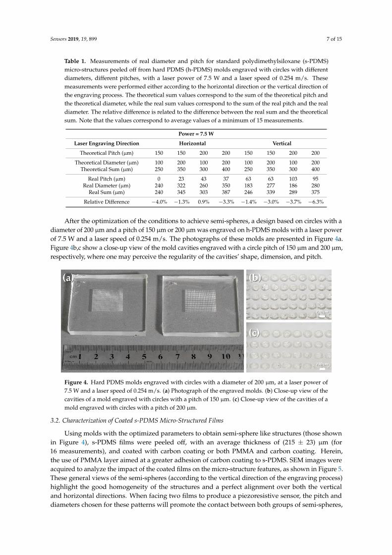
After the optimization of the conditions to achieve semi-spheres, a design based on circles with adiameter of 200 µm and a pitch of 150 µm or 200 µm was engraved on h-PDMS molds with a laser powerof 7.5 W and a laser speed of 0.254 m/s. The photographs of these molds are presented in Figure 4a.Figure 4b,c show a close-up view of the mold cavities engraved with a circle pitch of 150 µm and 200 µm,respectively, where one may perceive the regularity of the cavities’ shape, dimension, and pitch.
Sensors 2019, 19, x FOR PEER REVIEW 7 of 16
Table 1. Measurements of real diameter and pitch for standard polydimethylsiloxane (s-PDMS) micro-structures peeled off from hard PDMS (h-PDMS) molds engraved with circles with different diameters, different pitches, with a laser power of 7.5 W and a laser speed of 0.254 m/s. These measurements were performed either according to the horizontal direction or the vertical direction of the engraving process. The theoretical sum values correspond to the sum of the theoretical pitch and the theoretical diameter, while the real sum values correspond to the sum of the real pitch and the real diameter. The relative difference is related to the difference between the real sum and the theoretical sum. Note that the values correspond to average values of a minimum of 15 measurements.
Power = 7.5 W Laser Engraving Direction Horizontal Vertical
Theoretical Pitch (µm) 150 150 200 200 150 150 200 200 Theoretical Diameter (µm) 100 200 100 200 100 200 100 200
Theoretical Sum (µm) 250 350 300 400 250 350 300 400 Real Pitch (µm) 0 23 43 37 63 63 103 95
Real Diameter (µm) 240 322 260 350 183 277 186 280 Real Sum (µm) 240 345 303 387 246 339 289 375
Relative Difference −4.0% −1.3% 0.9% −3.3% −1.4% −3.0% −3.7% −6.3%
After the optimization of the conditions to achieve semi-spheres, a design based on circles with a diameter of 200 µm and a pitch of 150 µm or 200 µm was engraved on h-PDMS molds with a laser power of 7.5 W and a laser speed of 0.254 m/s. The photographs of these molds are presented in Figure 4a. Figure 4b,c show a close-up view of the mold cavities engraved with a circle pitch of 150 µm and 200 µm, respectively, where one may perceive the regularity of the cavities’ shape, dimension, and pitch.
Figure 4. Hard PDMS molds engraved with circles with a diameter of 200 µm, at a laser power of 7.5 W and a laser speed of 0.254 m/s. (a) Photograph of the engraved molds. (b) Close-up view of the cavities of a mold engraved with circles with a pitch of 150 µm. (c) Close-up view of the cavities of a mold engraved with circles with a pitch of 200 µm.
3.2. Characterization of Coated s-PDMS Micro-Structured Films
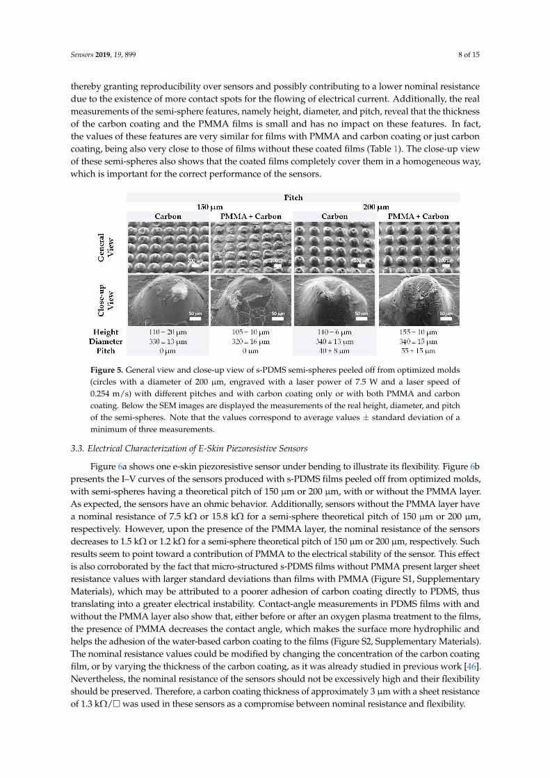
Using molds with the optimized parameters to obtain semi-sphere like structures (those shown in Figure 4), s-PDMS films were peeled off, with an average thickness of (215 ± 23) µm (for 16 measurements), and coated with carbon coating or both PMMA and carbon coating. Herein, the use of PMMA layer aimed at a greater adhesion of carbon coating to s-PDMS. SEM images were acquired to analyze the impact of the coated films on the micro-structure features, as shown in Figure 5. These general views of the semi-spheres (according to the vertical direction of the engraving process) highlight the good homogeneity of the structures and a perfect alignment over both the vertical and horizontal directions. When facing two films to produce a piezoresistive sensor, the pitch and diameters chosen for these patterns will promote the contact between both groups of semi-spheres,
Figure 4. Hard PDMS molds engraved with circles with a diameter of 200 µm, at a laser power of7.5 W and a laser speed of 0.254 m/s. (a) Photograph of the engraved molds. (b) Close-up view of thecavities of a mold engraved with circles with a pitch of 150 µm. (c) Close-up view of the cavities of amold engraved with circles with a pitch of 200 µm.
3.2. Characterization of Coated s-PDMS Micro-Structured Films
Using molds with the optimized parameters to obtain semi-sphere like structures (those shownin Figure 4), s-PDMS films were peeled off, with an average thickness of (215 ± 23) µm (for16 measurements), and coated with carbon coating or both PMMA and carbon coating. Herein,the use of PMMA layer aimed at a greater adhesion of carbon coating to s-PDMS. SEM images wereacquired to analyze the impact of the coated films on the micro-structure features, as shown in Figure 5.These general views of the semi-spheres (according to the vertical direction of the engraving process)highlight the good homogeneity of the structures and a perfect alignment over both the verticaland horizontal directions. When facing two films to produce a piezoresistive sensor, the pitch anddiameters chosen for these patterns will promote the contact between both groups of semi-spheres,
Sensors 2019, 19, 899 8 of 15
thereby granting reproducibility over sensors and possibly contributing to a lower nominal resistancedue to the existence of more contact spots for the flowing of electrical current. Additionally, the realmeasurements of the semi-sphere features, namely height, diameter, and pitch, reveal that the thicknessof the carbon coating and the PMMA films is small and has no impact on these features. In fact,the values of these features are very similar for films with PMMA and carbon coating or just carboncoating, being also very close to those of films without these coated films (Table 1). The close-up viewof these semi-spheres also shows that the coated films completely cover them in a homogeneous way,which is important for the correct performance of the sensors.
Sensors 2019, 19, x FOR PEER REVIEW 8 of 16
thereby granting reproducibility over sensors and possibly contributing to a lower nominal resistance due to the existence of more contact spots for the flowing of electrical current. Additionally, the real measurements of the semi-sphere features, namely height, diameter, and pitch, reveal that the thickness of the carbon coating and the PMMA films is small and has no impact on these features. In fact, the values of these features are very similar for films with PMMA and carbon coating or just carbon coating, being also very close to those of films without these coated films (Table 1). The close-up view of these semi-spheres also shows that the coated films completely cover them in a homogeneous way, which is important for the correct performance of the sensors.
Figure 5. General view and close-up view of s-PDMS semi-spheres peeled off from optimized molds (circles with a diameter of 200 µm, engraved with a laser power of 7.5 W and a laser speed of 0.254 m/s) with different pitches and with carbon coating only or with both PMMA and carbon coating. Below the SEM images are displayed the measurements of the real height, diameter, and pitch of the semi-spheres. Note that the values correspond to average values ± standard deviation of a minimum of three measurements.
3.3. Electrical Characterization of E-Skin Piezoresistive Sensors
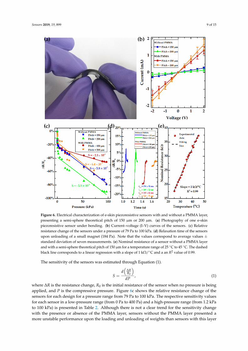
Figure 6a shows one e-skin piezoresistive sensor under bending to illustrate its flexibility. Figure 6b presents the I–V curves of the sensors produced with s-PDMS films peeled off from optimized molds, with semi-spheres having a theoretical pitch of 150 µm or 200 µm, with or without the PMMA layer. As expected, the sensors have an ohmic behavior. Additionally, sensors without the PMMA layer have a nominal resistance of 7.5 kΩ or 15.8 kΩ for a semi-sphere theoretical pitch of 150 µm or 200 µm, respectively. However, upon the presence of the PMMA layer, the nominal resistance of the sensors decreases to 1.5 kΩ or 1.2 kΩ for a semi-sphere theoretical pitch of 150 µm or 200 µm, respectively. Such results seem to point toward a contribution of PMMA to the electrical stability of the sensor. This effect is also corroborated by the fact that micro-structured s-PDMS films without PMMA present larger sheet resistance values with larger standard deviations than films with PMMA (Figure S1, Supplementary Materials), which may be attributed to a poorer adhesion of carbon coating directly to PDMS, thus translating into a greater electrical instability. Contact-angle measurements in PDMS films with and without the PMMA layer also show that, either before or after an oxygen plasma treatment to the films, the presence of PMMA decreases the contact angle, which makes the surface more hydrophilic and helps the adhesion of the water-based carbon coating to the films (Figure S2, Supplementary Materials). The nominal resistance values could be modified by changing the concentration of the carbon coating film, or by varying the thickness of the carbon coating, as it was already studied in previous work [46]. Nevertheless, the nominal resistance of the sensors should not be excessively high and their flexibility should be preserved. Therefore, a carbon coating thickness of approximately 3 µm with a sheet resistance of 1.3 kΩ/ was used in these sensors as a compromise between nominal resistance and flexibility.
Figure 5. General view and close-up view of s-PDMS semi-spheres peeled off from optimized molds(circles with a diameter of 200 µm, engraved with a laser power of 7.5 W and a laser speed of0.254 m/s) with different pitches and with carbon coating only or with both PMMA and carboncoating. Below the SEM images are displayed the measurements of the real height, diameter, and pitchof the semi-spheres. Note that the values correspond to average values ± standard deviation of aminimum of three measurements.
3.3. Electrical Characterization of E-Skin Piezoresistive Sensors
Figure 6a shows one e-skin piezoresistive sensor under bending to illustrate its flexibility. Figure 6bpresents the I–V curves of the sensors produced with s-PDMS films peeled off from optimized molds,with semi-spheres having a theoretical pitch of 150 µm or 200 µm, with or without the PMMA layer.As expected, the sensors have an ohmic behavior. Additionally, sensors without the PMMA layer havea nominal resistance of 7.5 kΩ or 15.8 kΩ for a semi-sphere theoretical pitch of 150 µm or 200 µm,respectively. However, upon the presence of the PMMA layer, the nominal resistance of the sensorsdecreases to 1.5 kΩ or 1.2 kΩ for a semi-sphere theoretical pitch of 150 µm or 200 µm, respectively. Suchresults seem to point toward a contribution of PMMA to the electrical stability of the sensor. This effectis also corroborated by the fact that micro-structured s-PDMS films without PMMA present larger sheetresistance values with larger standard deviations than films with PMMA (Figure S1, SupplementaryMaterials), which may be attributed to a poorer adhesion of carbon coating directly to PDMS, thustranslating into a greater electrical instability. Contact-angle measurements in PDMS films with andwithout the PMMA layer also show that, either before or after an oxygen plasma treatment to the films,the presence of PMMA decreases the contact angle, which makes the surface more hydrophilic andhelps the adhesion of the water-based carbon coating to the films (Figure S2, Supplementary Materials).The nominal resistance values could be modified by changing the concentration of the carbon coatingfilm, or by varying the thickness of the carbon coating, as it was already studied in previous work [46].Nevertheless, the nominal resistance of the sensors should not be excessively high and their flexibilityshould be preserved. Therefore, a carbon coating thickness of approximately 3 µm with a sheet resistanceof 1.3 kΩ/ was used in these sensors as a compromise between nominal resistance and flexibility.
Sensors 2019, 19, 899 9 of 15Sensors 2019, 19, x FOR PEER REVIEW 9 of 16
Figure 6. Electrical characterization of e-skin piezoresistive sensors with and without a PMMA layer, presenting a semi-sphere theoretical pitch of 150 µm or 200 µm. (a) Photography of one e-skin piezoresistive sensor under bending. (b) Current–voltage (I–V) curves of the sensors. (c) Relative resistance change of the sensors under a pressure of 79 Pa to 100 kPa. (d) Relaxation time of the sensors upon unloading of a small magnet (184 Pa). Note that the values correspond to average values ± standard deviation of seven measurements. (e) Nominal resistance of a sensor without a PMMA layer and with a semi-sphere theoretical pitch of 150 µm for a temperature range of 25 °C to 45 °C. The dashed black line corresponds to a linear regression with a slope of 1 kΩ/°C and a an R2 value of 0.99.
The sensitivity of the sensors was estimated through Equation (1).
𝑆 = 𝑑 ∆𝑅𝑅𝑑𝑃 , (1)
where ∆R is the resistance change, R0 is the initial resistance of the sensor when no pressure is being applied, and P is the compressive pressure. Figure 6c shows the relative resistance change of the sensors for each design for a pressure range from 79 Pa to 100 kPa. The respective sensitivity values for each sensor in a low-pressure range (from 0 Pa to 400 Pa) and a high-pressure range (from 1.2 kPa to 100 kPa) is presented in Table 2. Although there is not a clear trend for the sensitivity change with the presence or absence of the PMMA layer, sensors without the PMMA layer presented a more
Figure 6. Electrical characterization of e-skin piezoresistive sensors with and without a PMMA layer,presenting a semi-sphere theoretical pitch of 150 µm or 200 µm. (a) Photography of one e-skinpiezoresistive sensor under bending. (b) Current–voltage (I–V) curves of the sensors. (c) Relativeresistance change of the sensors under a pressure of 79 Pa to 100 kPa. (d) Relaxation time of the sensorsupon unloading of a small magnet (184 Pa). Note that the values correspond to average values ±standard deviation of seven measurements. (e) Nominal resistance of a sensor without a PMMA layerand with a semi-sphere theoretical pitch of 150 µm for a temperature range of 25 C to 45 C. The dashedblack line corresponds to a linear regression with a slope of 1 kΩ/C and a an R2 value of 0.99.
The sensitivity of the sensors was estimated through Equation (1).
S =d(
∆RR0
)dP
, (1)
where ∆R is the resistance change, R0 is the initial resistance of the sensor when no pressure is beingapplied, and P is the compressive pressure. Figure 6c shows the relative resistance change of thesensors for each design for a pressure range from 79 Pa to 100 kPa. The respective sensitivity valuesfor each sensor in a low-pressure range (from 0 Pa to 400 Pa) and a high-pressure range (from 1.2 kPato 100 kPa) is presented in Table 2. Although there is not a clear trend for the sensitivity changewith the presence or absence of the PMMA layer, sensors without the PMMA layer presented amore unstable performance upon the loading and unloading of weights than sensors with this layer
Sensors 2019, 19, 899 10 of 15
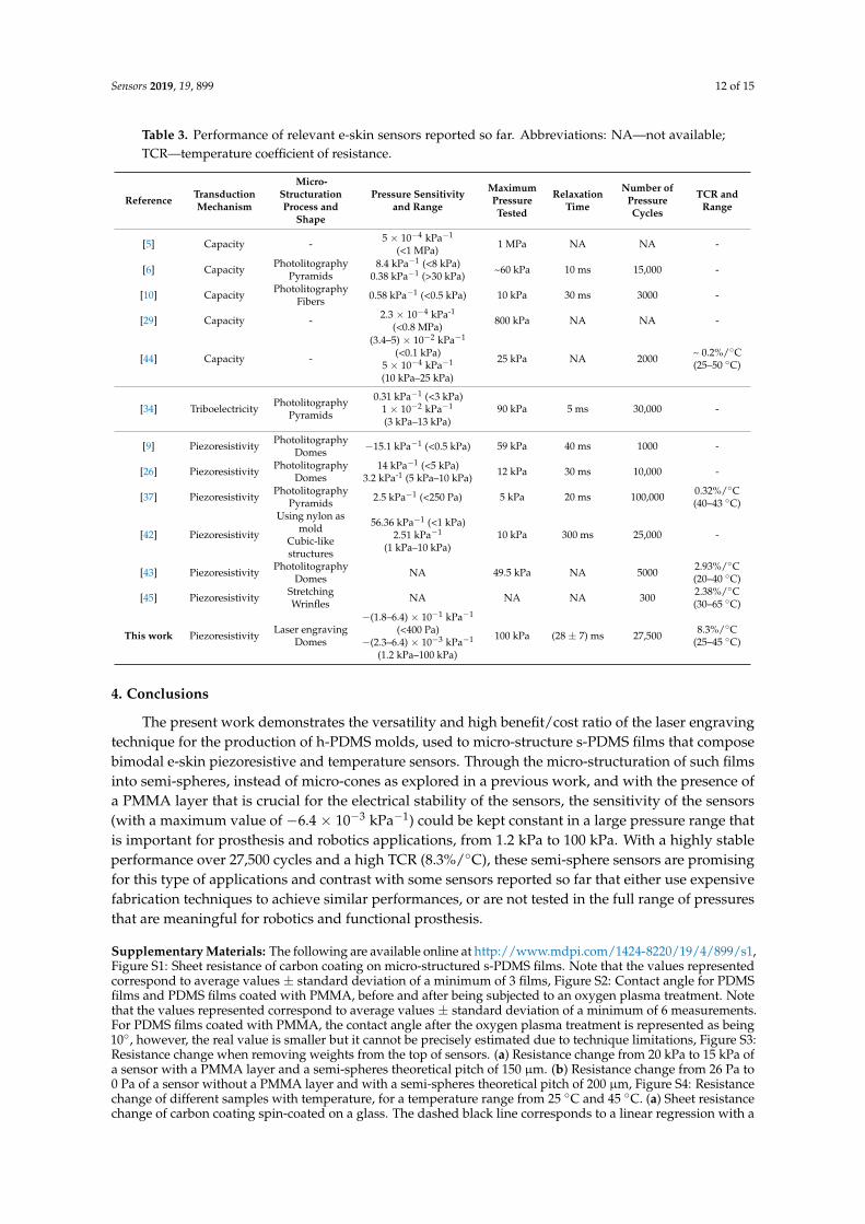
(Figure S3, Supplementary Materials). In fact, sensors without PMMA layer did not always maintainan approximately constant nominal resistance under a fixed pressure, showing some sudden resistancechanges that were associated with electrical instability of the carbon coating, since the sensors were notbeing stimulated. For sensors with the PMMA layer, their nominal resistance was kept constant duringa fixed pressure, only showing sudden changes when the weight was unloaded. There is also no cleartrend for the sensitivity change with the semi-sphere theoretical pitch; however, the results highlightthe fact that the sensors have a very stable sensitivity value, as high as −6.4 × 10⁻³ kPa−1 throughouta long pressure range that falls between the relevant values for functional prosthesis and robotics, fromless than 10 kPa to 100 kPa [20,28]. Table 3 summarizes the performance of several e-skin like sensorsreported in the literature and compares them to the ones obtained herein, where one may notice that thesensitivity values reached in this work are 10 times better than that of some reported sensors [5,29,44],being also constant over a wider pressure range, while other sensors suffer a sensitivity decrease below10 kPa [26,34,42]. Additionally, the majority of sensors reported so far were not tested in the full rangeof pressures that are relevant for these applications (10 kPa to 100 kPa), as shown in Table 3. Similare-skin sensors to those presented herein, but having micro-structures with the shape of cones insteadof semi-spheres, can reach higher sensitivities but in a reduced pressure range, with a maximum of−2.52 kPa−1 below 160 Pa, as this group already reported [46]. Such facts demonstrate that the laserengraving technique allows a great customization of the micro-structuration design, which has a directimpact in the performance of the sensors. Furthermore, the local defects that could be observed in themicro-structured s-PDMS films in Figure 3 did not hamper the sensing performance of the sensors,which highlights the high benefit/cost ratio of this micro-structuration technique.
Table 2. Sensitivities of the sensors shown in Figure 6c for the low-pressure range (from 0 Pa to 400 Pa)and the high-pressure range (from 1.2 kPa to 100 kPa).
Without PMMA With PMMA
Theoretical Pitch (µm) 150 200 150 200
Low Pressure(0 kPa–0.4 kPa) Sensitivity (kPa−1) −4.8 × 10⁻¹ −6.4 × 10⁻¹ −5.4 × 10⁻¹ −1.8 × 10⁻¹
High Pressure(1.2 kPa–100 kPa) Sensitivity (kPa−1) −5.8 × 10⁻³ −5.8 × 10⁻³ −2.3 × 10⁻³ −6.4 × 10⁻³
The relaxation time of each sensor was estimated by loading and unloading a small magnet(184 Pa) on top of them, as shown in Figure 6d. Sensors with the PMMA layer present slightly betterrelaxation times than sensors without the presence of such layer, reaching a low value of (28 ± 7) msfor a semi-sphere pitch of 200 µm. This value is better than some relaxation times reported for othersensors [9,10,26,42], as shown in Table 3. Furthermore, the presence of the PMMA layer seems tosmooth the sensors’ behavior during relaxation, while sensors without PMMA have a peak beforestabilizing their resistance. Such behavior may be explained by a contribution of PMMA for thereduction of the viscoelastic behavior that PDMS has when used alone [28,51].
Figure 6e shows the nominal resistance change of one sensor (without the PMMA layer and withsemi-spheres with a theoretical pitch of 150 µm) with temperature. The data show that these pressuresensors may also be used to monitor temperature due to their excellent linearity between their nominalresistance in the absence of a pressure and the applied temperature in one side of the sensor, with anR2 value very close to 1 and a slope of 1 kΩ/C. The temperature coefficient of resistance (TCR) maybe estimated through Equation (2).
TCR =∆RR0
T − T0, (2)
where ∆R is the resistance change, R0 is the initial resistance of the sensor, T is the temperature at whichthe sensor was heated, and T0 is the initial temperature of the sensor. A TCR of 8.3%/C was reached withthe sensor tested in Figure 6e, which is quite high when compared to other reported values [37,43–45]
Sensors 2019, 19, 899 11 of 15
as shown in Table 3. The detection of temperature changes by the sensor could be attributed to threeeffects: a sheet resistance change of the active material of the sensor (the carbon coating film) with thetemperature, a thermal expansion of PDMS (with a coefficient of thermal expansion of 3 × 10⁻⁴ C−1 [52])that induces a stretching of the carbon coating, thus leading to an increase in the carbon coating sheetresistance, and a change in the contact resistance between the semi-spheres of the sensor (please consultFigure S4, Supplementary Materials, for further details). The estimation of the contribution of each effectto the final performance of the sensor is not trivial and would require the establishment of a complexmathematic model of the sensor. Nonetheless, the data shown validate this e-skin sensor as a sensitivetemperature sensor within the range of human body temperatures.
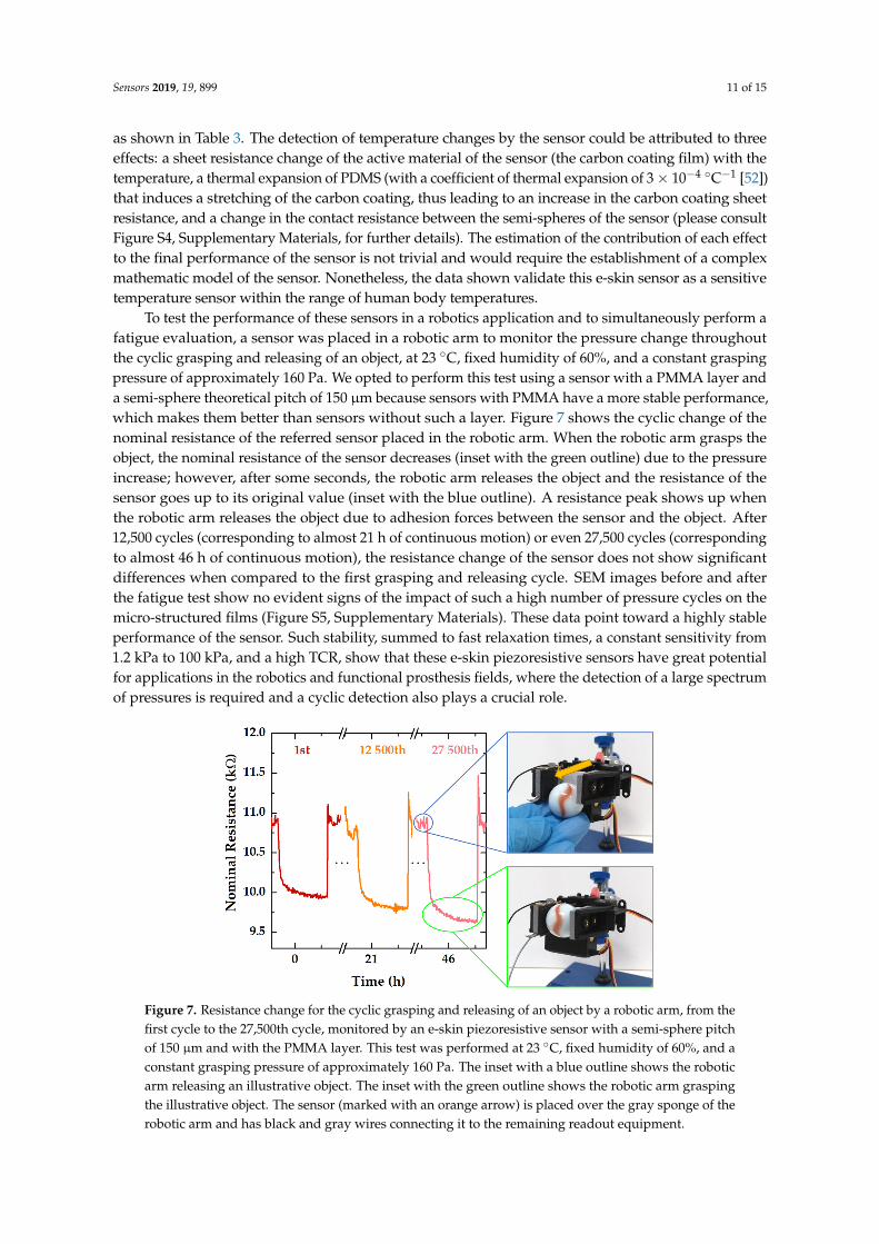
To test the performance of these sensors in a robotics application and to simultaneously perform afatigue evaluation, a sensor was placed in a robotic arm to monitor the pressure change throughoutthe cyclic grasping and releasing of an object, at 23 C, fixed humidity of 60%, and a constant graspingpressure of approximately 160 Pa. We opted to perform this test using a sensor with a PMMA layer anda semi-sphere theoretical pitch of 150 µm because sensors with PMMA have a more stable performance,which makes them better than sensors without such a layer. Figure 7 shows the cyclic change of thenominal resistance of the referred sensor placed in the robotic arm. When the robotic arm grasps theobject, the nominal resistance of the sensor decreases (inset with the green outline) due to the pressureincrease; however, after some seconds, the robotic arm releases the object and the resistance of thesensor goes up to its original value (inset with the blue outline). A resistance peak shows up whenthe robotic arm releases the object due to adhesion forces between the sensor and the object. After12,500 cycles (corresponding to almost 21 h of continuous motion) or even 27,500 cycles (correspondingto almost 46 h of continuous motion), the resistance change of the sensor does not show significantdifferences when compared to the first grasping and releasing cycle. SEM images before and afterthe fatigue test show no evident signs of the impact of such a high number of pressure cycles on themicro-structured films (Figure S5, Supplementary Materials). These data point toward a highly stableperformance of the sensor. Such stability, summed to fast relaxation times, a constant sensitivity from1.2 kPa to 100 kPa, and a high TCR, show that these e-skin piezoresistive sensors have great potentialfor applications in the robotics and functional prosthesis fields, where the detection of a large spectrumof pressures is required and a cyclic detection also plays a crucial role.
Sensors 2019, 19, x FOR PEER REVIEW 11 of 16
reached with the sensor tested in Figure 6e, which is quite high when compared to other reported values [37,43–45] as shown in Table 3. The detection of temperature changes by the sensor could be attributed to three effects: a sheet resistance change of the active material of the sensor (the carbon coating film) with the temperature, a thermal expansion of PDMS (with a coefficient of thermal expansion of 3 × 10⁻⁴ °C−1 [52]) that induces a stretching of the carbon coating, thus leading to an increase in the carbon coating sheet resistance, and a change in the contact resistance between the semi-spheres of the sensor (please consult Figure S4, Supplementary Materials, for further details). The estimation of the contribution of each effect to the final performance of the sensor is not trivial and would require the establishment of a complex mathematic model of the sensor. Nonetheless, the data shown validate this e-skin sensor as a sensitive temperature sensor within the range of human body temperatures. To test the performance of these sensors in a robotics application and to simultaneously perform a fatigue evaluation, a sensor was placed in a robotic arm to monitor the pressure change throughout the cyclic grasping and releasing of an object, at 23 °C, fixed humidity of 60%, and a constant grasping pressure of approximately 160 Pa. We opted to perform this test using a sensor with a PMMA layer and a semi-sphere theoretical pitch of 150 µm because sensors with PMMA have a more stable performance, which makes them better than sensors without such a layer. Figure 7 shows the cyclic change of the nominal resistance of the referred sensor placed in the robotic arm. When the robotic arm grasps the object, the nominal resistance of the sensor decreases (inset with the green outline) due to the pressure increase; however, after some seconds, the robotic arm releases the object and the resistance of the sensor goes up to its original value (inset with the blue outline). A resistance peak shows up when the robotic arm releases the object due to adhesion forces between the sensor and the object. After 12,500 cycles (corresponding to almost 21 h of continuous motion) or even 27,500 cycles (corresponding to almost 46 h of continuous motion), the resistance change of the sensor does not show significant differences when compared to the first grasping and releasing cycle. SEM images before and after the fatigue test show no evident signs of the impact of such a high number of pressure cycles on the micro-structured films (Figure S5, Supplementary Materials). These data point toward a highly stable performance of the sensor. Such stability, summed to fast relaxation times, a constant sensitivity from 1.2 kPa to 100 kPa, and a high TCR, show that these e-skin piezoresistive sensors have great potential for applications in the robotics and functional prosthesis fields, where the detection of a large spectrum of pressures is required and a cyclic detection also plays a crucial role.
Figure 7. Resistance change for the cyclic grasping and releasing of an object by a robotic arm, from the first cycle to the 27,500th cycle, monitored by an e-skin piezoresistive sensor with a semi-sphere pitch of 150 µm and with the PMMA layer. This test was performed at 23 °C, fixed humidity of 60%, and a constant grasping pressure of approximately 160 Pa. The inset with a blue outline shows the robotic arm releasing an illustrative object. The inset with the green outline shows the robotic arm grasping the illustrative object. The sensor (marked with an orange arrow) is placed over the gray
Figure 7. Resistance change for the cyclic grasping and releasing of an object by a robotic arm, from thefirst cycle to the 27,500th cycle, monitored by an e-skin piezoresistive sensor with a semi-sphere pitchof 150 µm and with the PMMA layer. This test was performed at 23 C, fixed humidity of 60%, and aconstant grasping pressure of approximately 160 Pa. The inset with a blue outline shows the roboticarm releasing an illustrative object. The inset with the green outline shows the robotic arm graspingthe illustrative object. The sensor (marked with an orange arrow) is placed over the gray sponge of therobotic arm and has black and gray wires connecting it to the remaining readout equipment.
Sensors 2019, 19, 899 12 of 15
Table 3. Performance of relevant e-skin sensors reported so far. Abbreviations: NA—not available;TCR—temperature coefficient of resistance.
Reference TransductionMechanism
Micro-StructurationProcess and
Shape
Pressure Sensitivityand Range
MaximumPressureTested
RelaxationTime
Number ofPressureCycles
TCR andRange
[5] Capacity - 5 × 10⁻⁴ kPa−1
(<1 MPa)1 MPa NA NA -
[6] Capacity PhotolitographyPyramids
8.4 kPa−1 (<8 kPa)0.38 kPa−1 (>30 kPa)
~60 kPa 10 ms 15,000 -
[10] Capacity PhotolitographyFibers 0.58 kPa−1 (<0.5 kPa) 10 kPa 30 ms 3000 -
[29] Capacity - 2.3 × 10⁻⁴ kPa-1
(<0.8 MPa)800 kPa NA NA -
[44] Capacity -
(3.4–5) × 10−2 kPa−1
(<0.1 kPa)5 × 10⁻⁴ kPa−1
(10 kPa–25 kPa)
25 kPa NA 2000 ~ 0.2%/C(25–50 C)
[34] Triboelectricity PhotolitographyPyramids
0.31 kPa−1 (<3 kPa)1 × 10⁻² kPa−1
(3 kPa–13 kPa)90 kPa 5 ms 30,000 -
[9] Piezoresistivity PhotolitographyDomes −15.1 kPa−1 (<0.5 kPa) 59 kPa 40 ms 1000 -
[26] Piezoresistivity PhotolitographyDomes
14 kPa−1 (<5 kPa)3.2 kPa-1 (5 kPa–10 kPa)
12 kPa 30 ms 10,000 -
[37] Piezoresistivity PhotolitographyPyramids 2.5 kPa−1 (<250 Pa) 5 kPa 20 ms 100,000 0.32%/C
(40–43 C)
[42] Piezoresistivity
Using nylon asmold
Cubic-likestructures
56.36 kPa−1 (<1 kPa)2.51 kPa−1
(1 kPa–10 kPa)10 kPa 300 ms 25,000 -
[43] Piezoresistivity PhotolitographyDomes NA 49.5 kPa NA 5000 2.93%/C
(20–40 C)
[45] Piezoresistivity StretchingWrinfles NA NA NA 300 2.38%/C
(30–65 C)
This work Piezoresistivity Laser engravingDomes
−(1.8–6.4) × 10−1 kPa−1
(<400 Pa)−(2.3–6.4) × 10−3 kPa−1
(1.2 kPa–100 kPa)
100 kPa (28 ± 7) ms 27,500 8.3%/C(25–45 C)
4. Conclusions
The present work demonstrates the versatility and high benefit/cost ratio of the laser engravingtechnique for the production of h-PDMS molds, used to micro-structure s-PDMS films that composebimodal e-skin piezoresistive and temperature sensors. Through the micro-structuration of such filmsinto semi-spheres, instead of micro-cones as explored in a previous work, and with the presence ofa PMMA layer that is crucial for the electrical stability of the sensors, the sensitivity of the sensors(with a maximum value of −6.4 × 10⁻³ kPa−1) could be kept constant in a large pressure range thatis important for prosthesis and robotics applications, from 1.2 kPa to 100 kPa. With a highly stableperformance over 27,500 cycles and a high TCR (8.3%/C), these semi-sphere sensors are promisingfor this type of applications and contrast with some sensors reported so far that either use expensivefabrication techniques to achieve similar performances, or are not tested in the full range of pressuresthat are meaningful for robotics and functional prosthesis.
Supplementary Materials: The following are available online at http://www.mdpi.com/1424-8220/19/4/899/s1,Figure S1: Sheet resistance of carbon coating on micro-structured s-PDMS films. Note that the values representedcorrespond to average values ± standard deviation of a minimum of 3 films, Figure S2: Contact angle for PDMSfilms and PDMS films coated with PMMA, before and after being subjected to an oxygen plasma treatment. Notethat the values represented correspond to average values ± standard deviation of a minimum of 6 measurements.For PDMS films coated with PMMA, the contact angle after the oxygen plasma treatment is represented as being10, however, the real value is smaller but it cannot be precisely estimated due to technique limitations, Figure S3:Resistance change when removing weights from the top of sensors. (a) Resistance change from 20 kPa to 15 kPa ofa sensor with a PMMA layer and a semi-spheres theoretical pitch of 150 µm. (b) Resistance change from 26 Pa to0 Pa of a sensor without a PMMA layer and with a semi-spheres theoretical pitch of 200 µm, Figure S4: Resistancechange of different samples with temperature, for a temperature range from 25 C and 45 C. (a) Sheet resistancechange of carbon coating spin-coated on a glass. The dashed black line corresponds to a linear regression with a
Sensors 2019, 19, 899 13 of 15
slope of 0.87 Ω/C and a R2 of 0.90. (b) Sheet resistance of a semi-spheres s-PDMS film (pitch of 150 µm) coatedwith carbon coating. The dashed black line corresponds to a linear regression with a slope of 0.24 kΩ/C and a R2of 0.99. (c) Nominal resistance of a sensor without PMMA layer and with a semi-spheres theoretical pitch of 150µm. The dashed black line corresponds to a linear regression with a slope of 1 kΩ/C and a R2 of 0.99, Figure S5:SEM images of s-PDMS films with PMMA and carbon coating, peeled off from optimized molds (circles with adiameter of 200 µm, engraved with a laser power of 7.5 W and a laser speed of 0.254 m/s). (a) General view of afilm before applying cyclic pressure. (b) Close-up view of a film before applying cyclic pressure. (c) General viewof another film after applying cyclic pressure (27500 cycles of grasping and releasing of an object). (d) Close-upview of another film after applying cyclic pressure (27500 cycles of grasping and releasing of an object).
Author Contributions: Conceptualization, R.I. and H.A.; supervision, R.I. and H.A.; investigation, N.P., P.A.,and A.d.S.; formal analysis, N.P. and A.d.S.; software, N.P., R.S., and R.F.; visualization, N.P., R.S., and A.d.S.;validation, E.F. and R.M.; writing—original draft preparation, N.P. and A.d.S.; writing—review and editing, R.I.,H.A., P.A., R.F., E.F., and R.M.
Funding: This research was funded by FEDER funds through the COMPETE 2020 Program and NationalFunds through FCT (Portuguese Foundation for Science and Technology) under the project numberPOCI-01-0145-FEDER-007688, Reference UID/CTM/50025/2013NOVA.ID.FCT.
Acknowledgments: A.d.S. acknowledges the support from the Portuguese Foundation for Science and Technologyand MIT Portugal through the scholarship PD/BD/105876/2014.
Conflicts of Interest: The authors declare no conflict of interest.
References
1. Hammock, M.L.; Chortos, A.; Tee, B.C.K.; Tok, J.B.H.; Bao, Z. 25th anniversary article: The evolution ofelectronic skin (E-Skin): A brief history, design considerations, and recent progress. Adv. Mater. 2013, 25,5997–6038. [CrossRef] [PubMed]
2. Chortos, A.; Liu, J.; Bao, Z. Pursuing prosthetic electronic skin. Nat. Mater. 2016, 15, 937–951. [CrossRef][PubMed]
3. Someya, T.; Sekitani, T.; Iba, S.; Kato, Y.; Kawaguchi, H.; Sakurai, T. A large-area, flexible pressure sensormatrix with organic field-effect transistors for artificial skin applications. Proc. Natl. Acad. Sci. USA 2004,101, 9966–9970. [CrossRef] [PubMed]
4. Someya, T.; Kato, Y.; Sekitani, T.; Iba, S.; Noguchi, Y.; Murase, Y.; Kawaguchi, H.; Sakurai, T. Conformable,flexible, large-area networks of pressure and thermal sensors with organic transistor active matrixes.Proc. Natl. Acad. Sci. USA 2005, 102, 12321–12325. [CrossRef] [PubMed]
5. Hu, W.; Niu, X.; Zhao, R.; Pei, Q. Elastomeric transparent capacitive sensors based on an interpenetratingcomposite of silver nanowires and polyurethane. Appl. Phys. Lett. 2013, 102, 083303–083309. [CrossRef]
6. Schwartz, G.; Tee, B.C.-K.; Mei, J.; Appleton, A.L.; Kim, D.H.; Wang, H.; Bao, Z. Flexible polymer transistorswith high pressure sensitivity for application in electronic skin and health monitoring. Nat. Commun. 2013, 4,1859–1867. [CrossRef]
7. Yao, H.B.; Ge, J.; Wang, C.F.; Wang, X.; Hu, W.; Zheng, Z.J.; Ni, Y.; Yu, S.H. A flexible and highly pressure-sensitive graphene-polyurethane sponge based on fractured microstructure design. Adv. Mater. 2013, 25,6692–6698. [CrossRef]
8. Dagdeviren, C.; Su, Y.; Joe, P.; Yona, R.; Liu, Y.; Kim, Y.-S.; Huang, Y.Y.; Damadoran, A.R.; Xia, J.; Martin, L.W.;et al. Conformable amplified lead zirconate titanate sensors with enhanced piezoelectric response forcutaneous pressure monitoring. Nat. Commun. 2014, 5, 4496–4506. [CrossRef]
9. Park, J.; Lee, Y.; Hong, J.; Ha, M.; Jung, Y.D.; Lim, H.; Kim, S.Y.; Ko, H. Giant Tunneling Piezoresistance ofComposite Elastomers with Interlocked Microdome Arrays for Ultrasensitive and Multimodal ElectronicSkins. ACS Nano 2014, 8, 4689–4697. [CrossRef]
10. Pang, C.; Koo, J.H.; Nguyen, A.; Caves, J.M.; Kim, M.G.; Chortos, A.; Kim, K.; Wang, P.J.; Tok, J.B.H.; Bao, Z.Highly skin-conformal microhairy sensor for pulse signal amplification. Adv. Mater. 2015, 27, 634–640.[CrossRef]
11. Park, H.; Jeong, Y.R.; Yun, J.; Hong, S.Y.; Jin, S.; Lee, S.-J.; Zi, G.; Ha, J.S. Stretchable Array of Highly SensitivePressure Sensors Consisting of Polyaniline Nanofibers and Au-Coated. ACS Nano 2015, 9, 9974–9985.[CrossRef]
Sensors 2019, 19, 899 14 of 15
12. Kim, D.-I.; Trung, T.Q.; Hwang, B.-U.; Kim, J.-S.; Jeon, S.; Bae, J.; Park, J.-J.; Lee, N.-E. A Sensor Array UsingMulti-functional Field-effect Transistors with Ultrahigh Sensitivity and Precision for Bio-monitoring. Sci. Rep.2015, 5, 12705–12716. [CrossRef] [PubMed]
13. Cai, F.; Yi, C.; Liu, S.; Wang, Y.; Liu, L.; Liu, X.; Xu, X.; Wang, L. Ultrasensitive, passive and wearable sensorsfor monitoring human muscle motion and physiological signals. Biosens. Bioelectron. 2016, 77, 907–913.[CrossRef]
14. Shin, K.-Y.; Lee, J.S.; Jang, J. Highly sensitive, wearable and wireless pressure sensor using free-standingZnO nanoneedle/PVDF hybrid thin film for heart rate monitoring. Nano Energy 2016, 22, 95–104. [CrossRef]
15. Dagdeviren, C.; Joe, P.; Tuzman, O.L.; Park, K.; Lee, K.J.; Shi, Y.; Huang, Y.; Rogers, J.A. Recent progressin flexible and stretchable piezoelectric devices for mechanical energy harvesting, sensing and actuation.Extrem. Mech. Lett. 2016, 9, 269–281. [CrossRef]
16. Kim, J.; Lee, M.; Shim, H.J.; Ghaffari, R.; Cho, H.R.; Son, D.; Jung, Y.H.; Soh, M.; Choi, C.; Jung, S.; et al.Stretchable silicon nanoribbon electronics for skin prosthesis. Nat. Commun. 2014, 5, 5747–5758. [CrossRef][PubMed]
17. Gerratt, A.P.; Michaud, H.O.; Lacour, S.P. Elastomeric Electronic Skin for Prosthetic Tactile Sensation. Adv.Funct. Mater. 2015, 25, 2287–2295. [CrossRef]
18. Rocha, R.P.; Lopes, P.A.; De Almeida, A.T.; Tavakoli, M.; Majudu, C. Fabrication and characterization of bendingand pressure sensors for a soft prosthetic hand. J. Micromech. Microeng. 2018, 28, 034001–034011. [CrossRef]
19. Pang, C.; Lee, G.-Y.; Kim, T.; Kim, S.M.; Kim, H.N.; Ahn, S.-H.; Suh, K.-Y. A flexible and highly sensitivestrain-gauge sensor using reversible interlocking of nanofibres. Nat. Mater. 2012, 11, 795–801. [CrossRef]
20. Pan, L.; Chortos, A.; Yu, G.; Wang, Y.; Isaacson, S.; Allen, R.; Shi, Y.; Dauskardt, R.; Bao, Z. An ultra-sensitiveresistive pressure sensor based on hollow-sphere microstructure induced elasticity in conducting polymerfilm. Nat. Commun. 2014, 5, 3002–3010. [CrossRef]
21. Gong, S.; Schwalb, W.; Wang, Y.; Chen, Y.; Tang, Y.; Si, J.; Shirinzadeh, B.; Cheng, W. A wearable and highlysensitive pressure sensor with ultrathin gold nanowires. Nat. Commun. 2014, 5, 3132–3140. [CrossRef]
22. Wang, X.; Gu, Y.; Xiong, Z.; Cui, Z.; Zhang, T. Silk-molded flexible, ultrasensitive, and highly stable electronicskin for monitoring human physiological signals. Adv. Mater. 2014, 26, 1336–1342. [CrossRef]
23. Choong, C.-L.; Shim, M.-B.; Lee, B.-S.; Jeon, S.; Ko, D.-S.; Kang, T.-H.; Bae, J.; Lee, S.H.; Byun, K.-E.; Im, J.; et al.Highly stretchable resistive pressure sensors using a conductive elastomeric composite on a micropyramidarray. Adv. Mater. 2014, 26, 3451–3458. [CrossRef]
24. Yin, X.; Vinod, T.P.; Jelinek, R. A flexible high-sensitivity piezoresistive sensor comprising a Aunanoribbon-coated polymer sponge. J. Mater. Chem. C 2015, 3, 9247–9252. [CrossRef]
25. Chun, S.; Kim, Y.; Oh, H.-S.; Bae, G.; Park, W. A highly sensitive pressure sensor using a double-layeredgraphene structure for tactile sensing. Nanoscale 2015, 7, 11652–11659. [CrossRef]
26. Bae, G.Y.; Pak, S.W.; Kim, D.; Lee, G.; Kim, D.H.; Chung, Y.; Cho, K. Linearly and Highly Pressure-SensitiveElectronic Skin Based on a Bioinspired Hierarchical Structural Array. Adv. Mater. 2016, 28, 5300–5306.[CrossRef]
27. Huang, Z.; Gao, M.; Yan, Z.; Pan, T.; Khan, S.A.; Zhang, Y.; Zhang, H.; Lin, Y. Pyramid microstructure withsingle walled carbon nanotubes for flexible and transparent micro-pressure sensor with ultra-high sensitivity.Sens. Actuators A Phys. 2017, 266, 345–351. [CrossRef]
28. Mannsfeld, S.C.B.; Tee, B.C.-K.; Stoltenberg, R.M.; Chen, C.V.H.-H.; Barman, S.; Muir, B.V.O.; Sokolov, A.N.;Reese, C.; Bao, Z. Highly sensitive flexible pressure sensors with microstructured rubber dielectric layers.Nat. Mater. 2010, 9, 859–864. [CrossRef]
29. Lipomi, D.J.; Vosgueritchian, M.; Tee, B.C.-K.; Hellstrom, S.L.; Lee, J.A.; Fox, C.H.; Bao, Z. Skin-like pressureand strain sensors based on transparent elastic films of carbon nanotubes. Nat. Nanotechnol. 2011, 6, 788–792.[CrossRef]
30. Zang, Y.; Zhang, F.; Huang, D.; Gao, X.; Di, C.; Zhu, D. Flexible suspended gate organic thin-film transistorsfor ultra-sensitive pressure detection. Nat. Commun. 2015, 6, 6269–6278. [CrossRef]
31. Persano, L.; Dagdeviren, C.; Su, Y.; Zhang, Y.; Girardo, S.; Pisignano, D.; Huang, Y.; Rogers, J.A. Highperformance piezoelectric devices based on aligned arrays of nanofibers of poly(vinylidenefluoride-co-trifluoroethylene). Nat. Commun. 2013, 4, 1633–1643. [CrossRef]
32. Pi, Z.; Zhang, J.; Wen, C.; Zhang, Z.B.; Wu, D. Flexible piezoelectric nanogenerator made ofpoly(vinylidenefluoride-co-trifluoroethylene) (PVDF-TrFE) thin film. Nano Energy 2014, 7, 33–41. [CrossRef]
Sensors 2019, 19, 899 15 of 15
33. Fan, F.-R.; Lin, L.; Zhu, G.; Wu, W.; Zhang, R.; Wang, Z.L. Transparent Triboelectric Nanogenerators and Self-Powered Pressure Sensors based on Micropatterned Plastic Films. Nano Lett. 2012, 12, 3109–3114. [CrossRef]
34. Lin, L.; Xie, Y.; Wang, S.; Wu, W.; Niu, S.; Wen, X.; Wang, Z.L. Triboelectric Active Sensor Array for Self-Powered Static and Dynamic Pressure Detection and Tactile Imaging. ACS Nano 2013, 7, 8266–8274. [CrossRef]
35. Zhu, G.; Yang, W.Q.; Zhang, T.; Jing, Q.; Chen, J.; Zhou, Y.S.; Bai, P.; Wang, Z.L. Self-powered, ultrasensitive,flexible tactile sensors based on contact electrification. Nano Lett. 2014, 14, 3208–3213. [CrossRef]
36. Seol, M.-L.; Woo, J.-H.; Lee, D.-I.; Im, H.; Hur, J.; Choi, Y.-K. Nature-Replicated Nano-in-Micro Structures forTriboelectric Energy Harvesting. Small 2014, 10, 3887–3894. [CrossRef]
37. Kim, K.; Jung, M.; Kim, B.; Kim, J.; Shin, K.; Kwon, O.-S.; Jeon, S. Low-voltage, high-sensitivity andhigh-reliability bimodal sensor array with fully inkjet-printed flexible conducting electrode for low powerconsumption electronic skin. Nano Energy 2017, 41, 301–307. [CrossRef]
38. Zhou, Y.; He, J.; Wang, H.; Qi, K.; Nan, N.; You, X.; Shao, W.; Wang, L.; Ding, B.; Cui, S. Highly sensitive,self-powered and wearable electronic skin based on pressure-sensitive nanofiber woven fabric sensor.Sci. Rep. 2017, 7. [CrossRef]
39. Zhu, Y.; Li, J.; Cai, H.; Wu, Y.; Ding, H.; Pan, N.; Wang, X. Highly sensitive and skin-like pressure sensorbased on asymmetric double-layered structures of reduced graphite oxide. Sens. Actuators B Chem. 2018, 255,1262–1267. [CrossRef]
40. Liu, W.; Liu, N.; Yue, Y.; Rao, J.; Luo, C.; Zhang, H.; Yang, C.; Su, J.; Liu, Z.; Gao, Y. A flexible and highlysensitive pressure sensor based on elastic carbon foam. J. Mater. Chem. C 2018, 6, 1451–1459. [CrossRef]
41. Yu, G.; Hu, J.; Tan, J.; Gao, Y.; Lu, Y.; Xuan, F. A wearable pressure sensor based on ultra-violet/ozonemicrostructured carbon nanotube/polydimethylsiloxane arrays for electronic skins. Nanotechnology 2018, 29,115502–115513. [CrossRef]
42. Wang, L.; Jackman, J.A.; Tan, E.-L.; Park, J.H.; Potroz, M.G.; Hwang, E.T.; Cho, N.-J. High-performance,flexible electronic skin sensor incorporating natural microcapsule actuators. Nano Energy 2017, 36, 38–45.[CrossRef]
43. Park, J.; Kim, M.; Lee, Y.; Lee, H.S.; Ko, H. Fingertip skin-inspired microstructured ferroelectric skinsdiscriminate static/dynamic pressure and temperature stimuli. Sci. Adv. 2015, 1, e1500661. [CrossRef]
44. Kim, S.Y.; Park, S.; Park, H.W.; Park, D.H.; Jeong, Y.; Kim, D.H. Highly Sensitive and Multimodal All-CarbonSkin Sensors Capable of Simultaneously Detecting Tactile and Biological Stimuli. Adv. Mater. 2015, 27,4178–4185. [CrossRef]
45. Gui, Q.; He, Y.; Gao, N.; Tao, X.; Wang, Y. A Skin-Inspired Integrated Sensor for Synchronous Monitoring ofMultiparameter Signals. Adv. Funct. Mater. 2017, 27, 1702050–1702058. [CrossRef]
46. Dos Santos, A.; Pinela, N.; Alves, P.; Santos, R.; Fortunato, E.; Martins, R.; Águas, H.; Igreja, R. PiezoresistiveE-Skin Sensors Produced with Laser Engraved Molds. Adv. Electron. Mater. 2018, 4, 1800182–1800192. [CrossRef]
47. Dos Santos, A.; Pinela, N.; Alves, P.; Santos, R.; Fortunato, E.; Martins, R.; Águas, H.; Igreja, R. E-SkinPressure Sensors Made by Laser Engraved PDMS Molds. Proceedings 2018, 2, 1039. [CrossRef]
48. Huft, J.; Da Costa, D.J.; Walker, D.; Hansen, C.L. Three-dimensional large-scale microfluidic integration bylaser ablation of interlayer connections. Lab Chip 2010, 10, 2358–2365. [CrossRef]
49. Fogarty, B.A.; Heppert, K.E.; Cory, T.J.; Hulbutta, K.R.; Martin, R.S.; Lunte, S.M. Rapid fabrication ofpoly(dimethylsiloxane)-based microchip capillary electrophoresis devices using CO2 laser ablation. Analyst2005, 130, 924–930. [CrossRef]
50. Riahi, M. CO2 Laser and Micro-Fluidics. In CO2 Laser-Optimisation and Application; Dumitras, D.C., Ed.;InTech: London, UK, 2012; pp. 307–324. ISBN 978-953-51-0351-6.
51. Ha, M.; Lim, S.; Park, J.; Um, D.-S.; Lee, Y.; Ko, H. Bioinspired Interlocked and Hierarchical Design of ZnONanowire Arrays for Static and Dynamic Pressure-Sensitive Electronic Skins. Adv. Funct. Mater. 2015, 25,2841–2849. [CrossRef]
52. Grzybowski, B.A.; Brittain, S.T.; Whitesides, G.M. Thermally actuated interferometric sensors based on thethermal expansion of transparent elastomeric media. Rev. Sci. Instrum. 1999, 70, 2031–2037. [CrossRef]
© 2019 by the authors. Licensee MDPI, Basel, Switzerland. This article is an open accessarticle distributed under the terms and conditions of the Creative Commons Attribution(CC BY) license (http://creativecommons.org/licenses/by/4.0/).


![INDEX [microdentsystem.com] · 2015-11-24 · INDEX PRESENTATION. INTRODUCTION MULTIPLE PROSTHESIS. REMOVABLE AND IMMEDIATE PROSTHESIS. SINGLE PROSTHESIS CEMENTED PROSTHESIS. Microdent](https://img.pdfslide.net/doc/110x75/5facd9ee77a5ed547a36b19c/index-2015-11-24-index-presentation-introduction-multiple-prosthesis-removable.jpg)