Embed Size (px)
Citation preview

EC21 Mini PCIe
Hardware Design
LTE Module Series
Rev. EC21_Mini_PCIe_Hardware_Design_V1.1
Date: 2017-01-24
www.quectel.com
LTE Module Series EC21 Mini PCIe Hardware Design
EC21_Mini_PCIe_Hardware_Design Confidential / Released 1 / 41
Our aim is to provide customers with timely and comprehensive service. For any
assistance, please contact our company headquarters:
Quectel Wireless Solutions Co., Ltd.
Office 501, Building 13, No.99, Tianzhou Road, Shanghai, China, 200233
Tel: +86 21 5108 6236
Email: [email protected]
Or our local office. For more information, please visit:
http://www.quectel.com/support/salesupport.aspx
For technical support, or to report documentation errors, please visit:
http://www.quectel.com/support/techsupport.aspx
Or email to: [email protected]
GENERAL NOTES
QUECTEL OFFERS THE INFORMATION AS A SERVICE TO ITS CUSTOMERS. THE INFORMATION
PROVIDED IS BASED UPON CUSTOMERS’ REQUIREMENTS. QUECTEL MAKES EVERY EFFORT
TO ENSURE THE QUALITY OF THE INFORMATION IT MAKES AVAILABLE. QUECTEL DOES NOT
MAKE ANY WARRANTY AS TO THE INFORMATION CONTAINED HEREIN, AND DOES NOT ACCEPT
ANY LIABILITY FOR ANY INJURY, LOSS OR DAMAGE OF ANY KIND INCURRED BY USE OF OR
RELIANCE UPON THE INFORMATION. THE INFORMATION SUPPLIED HEREIN IS SUBJECT TO
CHANGE WITHOUT PRIOR NOTICE.
COPYRIGHT
THE INFORMATION CONTAINED HERE IS PROPRIETARY TECHNICAL INFORMATION OF
QUECTEL CO., LTD. TRANSMITTING, REPRODUCTION, DISSEMINATION AND EDITING OF THIS
DOCUMENT AS WELL AS UTILIZATION OF THE CONTENT ARE FORBIDDEN WITHOUT
PERMISSION. OFFENDERS WILL BE HELD LIABLE FOR PAYMENT OF DAMAGES. ALL RIGHTS
ARE RESERVED IN THE EVENT OF A PATENT GRANT OR REGISTRATION OF A UTILITY MODEL
OR DESIGN.
Copyright © Quectel Wireless Solutions Co., Ltd. 2017. All rights reserved.
Quectel
Confidential
LTE Module Series EC21 Mini PCIe Hardware Design
EC21_Mini_PCIe_Hardware_Design Confidential / Released 2 / 41
About the Document
History
Revision Date Author Description
1.0 2016-06-07 Yeoman CHEN/
Frank WANG Initial
1.1 2017-01-24 Lyndon LIU/
Rex WANG
1. Deleted description of EC21-AUTL and EC21-CT
Mini PCIe in Table 1.
2. Updated key features of EC21 Mini PCIe in Table 2.
3. Added current consumption of EC21 Mini PCIe in
Chapter 4.7.
4. Updated mechanical dimensions of EC21 Mini PCIe
in Figure 15.
5. Updated conducted RF output power in Table 16.
6. Updated conducted RF receiving sensitivity of
EC21-A in Table 18.
7. Added conducted RF receiving sensitivity of
EC21-KL in Table 21.
8. Added conducted RF receiving sensitivity of
EC21-J in Table 22.
Quectel
Confidential

LTE Module Series EC21 Mini PCIe Hardware Design
EC21_Mini_PCIe_Hardware_Design Confidential / Released 3 / 41
Contents
About the Document ................................................................................................................................... 2
Contents ....................................................................................................................................................... 3
Table Index ................................................................................................................................................... 5
Figure Index ................................................................................................................................................. 6
1 Introduction .......................................................................................................................................... 7
1.1. Safety Information...................................................................................................................... 8
2 Product Concept .................................................................................................................................. 9
2.1. General Description ................................................................................................................... 9
2.2. Description of Product Series .................................................................................................. 10
2.3. Key Features ........................................................................................................................... 11
2.4. Functional Diagram ................................................................................................................. 13
3 Application Interface ......................................................................................................................... 14
3.1. General Description ................................................................................................................. 14
3.2. EC21 Mini PCIe Interface ........................................................................................................ 14
3.2.1. Definition of Interface ..................................................................................................... 14
3.2.2. Pin Assignment .............................................................................................................. 17
3.3. Power Supply ........................................................................................................................... 18
3.4. USIM Card Interface ................................................................................................................ 19
3.5. USB Interface .......................................................................................................................... 20
3.6. UART Interface ........................................................................................................................ 21
3.7. PCM and I2C Interfaces .......................................................................................................... 22
3.8. Control Signals ........................................................................................................................ 24
3.8.1. RI Signal ......................................................................................................................... 25
3.8.2. DTR Signal ..................................................................................................................... 25
3.8.3. W_DISABLE# Signal ...................................................................................................... 25
3.8.4. PERST# Signal .............................................................................................................. 25
3.8.5. LED_WWAN# Signal ..................................................................................................... 26
3.8.6. WAKE# Signal ................................................................................................................ 27
3.9. Antenna Interfaces .................................................................................................................. 27
4 Electrical and Radio Characteristics ............................................................................................... 29
4.1. General Description ................................................................................................................. 29
4.2. Power Supply Requirements ................................................................................................... 29
4.3. I/O Requirements ..................................................................................................................... 30
4.4. RF Characteristics ................................................................................................................... 30
4.5. GNSS Receiver ....................................................................................................................... 33
4.6. ESD Characteristics ................................................................................................................ 33
4.7. Current Consumption .............................................................................................................. 34
5 Dimensions and Packaging .............................................................................................................. 37
5.1. General Description ................................................................................................................. 37
Quectel
Confidential

LTE Module Series EC21 Mini PCIe Hardware Design
EC21_Mini_PCIe_Hardware_Design Confidential / Released 4 / 41
5.2. Mechanical Dimensions of EC21 Mini PCIe ............................................................................ 37
5.3. Standard Dimensions of Mini PCI Express ............................................................................. 38
5.4. Packaging Specification ........................................................................................................... 39
6 Appendix References ........................................................................................................................ 40
Quectel
Confidential

LTE Module Series EC21 Mini PCIe Hardware Design
EC21_Mini_PCIe_Hardware_Design Confidential / Released 5 / 41
Table Index
TABLE 1: DESCRIPTION OF EC21 MINI PCIE ................................................................................................ 10
TABLE 2: KEY FEATURES OF EC21 MINI PCIE .............................................................................................. 11
TABLE 3: DEFINITION OF I/O PARAMETERS ................................................................................................. 14
TABLE 4: DESCRIPTION OF PINS .................................................................................................................. 15
TABLE 5: DEFINITION OF VCC_3V3 AND GND PINS .................................................................................... 18
TABLE 6: USIM PIN DEFINITION ..................................................................................................................... 19
TABLE 7: PIN DEFINITION OF USB INTERFACE ........................................................................................... 20
TABLE 8: PIN DEFINITION OF THE UART INTERFACE ................................................................................. 21
TABLE 9: PIN DEFINITION OF PCM AND I2C INTERFACES ......................................................................... 22
TABLE 10: PIN DEFINITION OF CONTROL SIGNAL ...................................................................................... 24
TABLE 11: RADIO OPERATIONAL STATES ..................................................................................................... 25
TABLE 12: INDICATIONS OF NETWORK STATUS ......................................................................................... 26
TABLE 13: ANTENNA REQUIREMENTS .......................................................................................................... 27
TABLE 14: POWER SUPPLY REQUIREMENTS .............................................................................................. 29
TABLE 15: I/O REQUIREMENTS ...................................................................................................................... 30
TABLE 16: EC21 MINI PCIE CONDUCTED RF OUTPUT POWER ................................................................. 30
TABLE 17: EC21-E MINI PCIE CONDUCTED RF RECEIVING SENSITIVITY ................................................ 31
TABLE 18: EC21-A MINI PCIE CONDUCTED RF RECEIVING SENSITIVITY ................................................ 31
TABLE 19: EC21-V MINI PCIE CONDUCTED RF RECEIVING SENSITIVITY ................................................ 32
TABLE 20: EC21-AUT MINI PCIE CONDUCTED RF RECEIVING SENSITIVITY ........................................... 32
TABLE 21: EC21-KL MINI PCIE CONDUCTED RF RECEIVING SENSITIVITY .............................................. 32
TABLE 22: EC21-J MINI PCIE CONDUCTED RF RECEIVING SENSITIVITY ................................................ 33
TABLE 23: ESD CHARACTERISTICS OF EC21 MINI PCIE ............................................................................ 33
TABLE 24: CURRENT CONSUMPTION OF EC21-A MINI PCIE ..................................................................... 34
TABLE 25: CURRENT CONSUMPTION OF EC21-V MINI PCIE ..................................................................... 35
TABLE 26: CURRENT CONSUMPTION OF EC21-KL MINI PCIE ................................................................... 35
TABLE 27: GNSS CURRENT CONSUMPTION OF EC21 MINI PCIE SERIES MODULE ............................... 36
TABLE 28: RELATED DOCUMENTS ................................................................................................................ 40
TABLE 29: TERMS AND ABBREVIATIONS ...................................................................................................... 40
Quectel
Confidential

LTE Module Series EC21 Mini PCIe Hardware Design
EC21_Mini_PCIe_Hardware_Design Confidential / Released 6 / 41
Figure Index
FIGURE 1: FUNCTIONAL DIAGRAM ............................................................................................................... 13
FIGURE 2: PIN ASSIGNMENT ......................................................................................................................... 17
FIGURE 3: REFERENCE DESIGN OF POWER SUPPLY ............................................................................... 18
FIGURE 4: REFERENCE CIRCUIT OF USIM CARD INTERFACE WITH A 6-PIN USIM CARD CONNECTOR
........................................................................................................................................................................... 19
FIGURE 5: REFERENCE CIRCUIT OF USB INTERFACE .............................................................................. 20
FIGURE 6: TIMING IN PRIMARY MODE .......................................................................................................... 23
FIGURE 7: TIMING IN AUXILIARY MODE........................................................................................................ 23
FIGURE 8: REFERENCE CIRCUIT OF PCM APPLICATION WITH AUDIO CODEC ...................................... 24
FIGURE 9: RI BEHAVIOR ................................................................................................................................. 25
FIGURE 10: TIMING OF RESETTING MODULE ............................................................................................. 26
FIGURE 11: LED_WWAN# SIGNAL REFERENCE CIRCUIT DIAGRAM ......................................................... 26
FIGURE 12: WAKE# BEHAVIOR ...................................................................................................................... 27
FIGURE 13: DIMENSIONS OF THE RF CONNECTOR (UNIT: MM) ............................................................... 28
FIGURE 14: MECHANICALS OF UF.L-LP CONNECTORS ............................................................................. 28
FIGURE 15: MECHANICAL DIMENSIONS OF EC21 MINI PCIE (UNIT: MM) ................................................. 37
FIGURE 16: STANDARD DIMENSIONS OF MINI PCI EXPRESS (UNIT: MM) ............................................... 38
FIGURE 17: DIMENSIONS OF THE MINI PCI EXPRESS CONNECTOR (THE MOLEX 679100002, UNIT: MM)
........................................................................................................................................................................... 39
Quectel
Confidential
LTE Module Series EC21 Mini PCIe Hardware Design
EC21_Mini_PCIe_Hardware_Design Confidential / Released 7 / 41
1 Introduction
This document defines EC21 Mini PCIe module and describes its hardware interfaces which are
connected with your application and air interfaces.
This document can help you to quickly understand the interface specifications, electrical and mechanical
details and related product information of the EC21 Mini PCIe module. To facilitate its application in
different fields, relevant reference design documents are also provided. Associated with application note
and user guide of EC21 Mini PCIe module, you can use the module to design and set up mobile
applications easily.
Quectel
Confidential

LTE Module Series EC21 Mini PCIe Hardware Design
EC21_Mini_PCIe_Hardware_Design Confidential / Released 8 / 41
1.1. Safety Information
The following safety precautions must be observed during all phases of the operation, such as usage,
service or repair of any cellular terminal or mobile incorporating EC21 Mini PCIe module. Manufacturers
of the cellular terminal should send the following safety information to users and operating personnel, and
incorporate these guidelines into all manuals supplied with the product. If not so, Quectel does not take on
any liability for customer failure to comply with these precautions.
Full attention must be given to driving at all times in order to reduce the risk of an
accident. Using a mobile while driving (even with a handsfree kit) causes
distraction and can lead to an accident. You must comply with laws and regulations
restricting the use of wireless devices while driving.
Switch off the cellular terminal or mobile before boarding an aircraft. Make sure it is
switched off. The operation of wireless appliances in an aircraft is forbidden, so as
to prevent interference with communication systems. Consult the airline staff about
the use of wireless devices on boarding the aircraft, if your device offers an
Airplane Mode which must be enabled prior to boarding an aircraft.
Switch off your wireless device when in hospitals, clinics or other health care facilities. These requests are desinged to prevent possible interference with sensitive medical equipment.
Cellular terminals or mobiles operating over radio frequency signal and cellular
network cannot be guaranteed to connect in all conditions, for example no mobile
fee or with an invalid USIM/SIM card. While you are in this condition and need
emergent help, please remember using emergency call. In order to make or
receive a call, the cellular terminal or mobile must be switched on and in a service
area with adequate cellular signal strength.
Your cellular terminal or mobile contains a transmitter and receiver. When it is ON,
it receives and transmits radio frequency energy. RF interference can occur if it is
used close to TV set, radio, computer or other electric equipment.
In locations with potentially explosive atmospheres, obey all posted signs to turn
off wireless devices such as your phone or other cellular terminals. Areas with
potentially explosive atmospheres include fuelling areas, below decks on boats,
fuel or chemical transfer or storage facilities, areas where the air contains
chemicals or particles such as grain, dust or metal powders, etc.
Quectel
Confidential

LTE Module Series EC21 Mini PCIe Hardware Design
EC21_Mini_PCIe_Hardware_Design Confidential / Released 9 / 41
2 Product Concept
2.1. General Description
EC21 Mini PCIe module provides data connectivity on LTE-FDD, LTE-TDD, WCDMA and GSM networks
with PCI Express Mini Card 1.2 standard interface. It supports embedded operating systems such as
WinCE, Linux and Android etc., and also provides audio, high-speed data transmission and GNSS
functionality for your applications.
EC21 Mini PCIe module can be applied in the following fields:
PDAs and Laptop Computer
Remote Monitor System
Vehicle System
Wireless POS System
Intelligent Meter Reading System
Wireless Router and Switch
Other Wireless Terminal Devices
This chapter generally introduces the following aspects of EC21 Mini PCIe module:
Product Series
Key Features
Functional Diagram
EC21 Mini PCIe contains Telematics version and Data-only version. Telematics version supports voice
and data functions, while Data-only version only supports data function.
NOTE
Quectel
Confidential

LTE Module Series EC21 Mini PCIe Hardware Design
EC21_Mini_PCIe_Hardware_Design Confidential / Released 10 / 41
2.2. Description of Product Series
The following table shows the product series of EC21 Mini PCIe module.
Table 1: Description of EC21 Mini PCIe
Product Series Description
EC21-E Mini PCIe
Support GSM: 900/1800MHz
Support WCDMA: B1/B5/B8
Support LTE-FDD: B1/B3/B5/B7/B8/B20
Support LTE/WCDMA receive diversity
Support GNSS1)
Support digital audio2)
EC21-A Mini PCIe
Support WCDMA: B2/B4/B5
Support LTE-FDD: B2/B4/B12
Support LTE/WCDMA receive diversity
Support GNSS1)
Support digital audio2)
EC21-V Mini PCIe
Support LTE-FDD: B4/B13
Support LTE receive diversity
Support GNSS1)
Support digital audio2)
EC21-AUT Mini PCIe
Support WCDMA: B1/B5
Support LTE-FDD: B1/B3/B5/B7/B28
Support LTE/WCDMA receive diversity
Support GNSS1)
Support digital audio2)
EC21-AU Mini PCIe3)
Support GSM: 850/900/1800/1900MHz
Support WCDMA: B1/B2/B5/B8
Support LTE-FDD: B1/B2/B3/B4/B5/B7/B8/B28
Support LTE-TDD: B40
Support LTE/WCDMA receive diversity3)
Support GNSS1)
Support digital audio2)
EC21-J Mini PCIe
Support LTE-FDD: B1/B3/B8/B18/B19/B26
Support LTE receive diversity
Support digital audio2)
EC21-KL Mini PCIe
Support LTE-FDD: B1/B3/B5/B7/B8
Support LTE receive diversity
Support digital audio2)
Quectel
Confidential

LTE Module Series EC21 Mini PCIe Hardware Design
EC21_Mini_PCIe_Hardware_Design Confidential / Released 11 / 41
1. 1)
GNSS function is optional.
2. 2)
Digital audio (PCM) function is only supported in Telematics version.
3. 3)
B2 band on EC21-AU Mini PCIe module does not support receive diversity.
2.3. Key Features
The following table describes the detailed features of EC21 Mini PCIe module.
Table 2: Key Features of EC21 Mini PCIe
Feature Details
Function Interface PCI Express Mini Card 1.2 Standard Interface
Power Supply Supply voltage: 3.0~3.6V
Typical supply voltage: 3.3V
Transmitting Power
Class 4 (33dBm±2dB) for GSM850
Class 4 (33dBm±2dB) for GSM900
Class 1 (30dBm±2dB) for DCS1800
Class 1 (30dBm±2dB) for PCS1800
Class E2 (27dBm±3dB) for GSM850 8-PSK
Class E2 (27dBm±3dB) for GSM900 8-PSK
Class E2 (26dBm±3dB) for DCS1800 8-PSK
Class E2 (26dBm±3dB) for PCS1900 8-PSK
Class 3 (24dBm+1/-3dB) for WCDMA bands
Class 3 (23dBm±2dB) for LTE-FDD bands
Class 3 (23dBm±2dB) for LTE-TDD bands
LTE Features
Support up to non-CA Cat 1
Support 1.4 to 20MHz RF bandwidth
Support MIMO in DL direction
FDD: Max 5Mbps (UL), 10Mbps (DL)
TDD: Max 3.1Mbps (UL), 8.96Mbps (DL)
TDD: Max 3.1Mbps (UL), 8.96Mbps (DL)
WCDMA Features
Support 3GPP R8 DC-HSPA+
Support 16-QAM, 64-QAM and QPSK modulation
3GPP R6 Cat 6 HSUPA: Max 5.76Mbps (UL)
3GPP R8 Cat 24 DC-HSPA+: Max 42Mbps (DL)
GSM Features
R99:
CSD: 9.6kbps, 14.4kbps
GPRS:
NOTES
Quectel
Confidential

LTE Module Series EC21 Mini PCIe Hardware Design
EC21_Mini_PCIe_Hardware_Design Confidential / Released 12 / 41
Support GPRS multi-slot class 12 (12 by default)
Coding scheme: CS-1, CS-2, CS-3 and CS-4
Maximum of four Rx time slots per frame
EDGE:
Support EDGE multi-slot class 12 (12 by default)
Support GMSK and 8-PSK for different MCS (Modulation and Coding
Scheme)
Downlink coding schemes: CS 1-4 and MCS 1-9
Uplink coding schemes: CS 1-4 and MCS 1-9
Internet Protocol Features
Support TCP/UDP/PPP/FTP/HTTP/NTP/PING/QMI/HTTPS*/SMTP*/
MMS*/FTPS*/SSL* protocols
Support PAP (Password Authentication Protocol) and CHAP (Challenge
Handshake Authentication Protocol) protocols usually used for PPP
connections
SMS
Text and PDU mode
Point to point MO and MT
SMS cell broadcast
SMS storage: ME by default
USIM Interface Support USIM/SIM card: 1.8V, 3.0V
UART Interface Baud rate can reach up to 230400bps; 115200bps by default
Used for AT command communication
Audio Feature
Support one digital audio interface: PCM interface
GSM: HR/FR/EFR/AMR/AMR-WB
WCDMA: AMR/AMR-WB
LTE: AMR/AMR-WB
Support echo cancellation and noise suppression
PCM Interface
Support 8-bit A-law*, μ-law* and 16-bit linear data formats
Support long frame synchronization and short frame synchronization
Support master and slave mode, but must be the master in long frame
synchronization
USB Interface
Compliant with USB 2.0 specification (slave only), the data transfer rate
can reach up to 480Mbps
Used for AT command communication, data transmission, firmware
upgrade, software debugging, GNSS NMEA output and voice over USB*
USB Driver: Windows XP, Windows Vista, Windows 7, Windows 8/8.1,
Windows 10, Linux 2.6 or later, Android 4.0/4.2/4.4/5.0/5.1/6.0
Antenna Interface Include main antenna, diversity antenna and GNSS antenna
Rx-diversity Support LTE/WCDMA Rx-diversity
GNSS Features Gen 8C Lite of Qualcomm
Protocol: NMEA 0183
AT Commands Compliant with 3GPP TS 27.007, 27.005 and Quectel enhanced AT
commands
Quectel
Confidential

LTE Module Series EC21 Mini PCIe Hardware Design
EC21_Mini_PCIe_Hardware_Design Confidential / Released 13 / 41
1. “*” means under development.
2. 2)
Within operating temperature range, the module is 3GPP compliant.
3. 3)
Within extended temperature range, the module remains the ability to establish and maintain a
voice, SMS, data transmission, emergency call, etc. There is no unrecoverable malfunction; there are
also no effects on radio spectrum and no harm to radio network. Only one or more parameters like
Pout might reduce in their value and exceed the specified tolerances. When the temperature returns
to normal operating temperature levels, the module is compliant with 3GPP specification again.
2.4. Functional Diagram
The following figure shows the block diagram of EC21 Mini PCIe.
EC21
Module
PCM&I2C
Min
i PC
I Exp
ress
Inte
rface
USB
USIM
W_DISABLE#
PERST#
LED_WWAN#
Main
Antenna
Interface
VCC
Main
Antenna
VBAT
GNSS
Antenna
Interface
GNSS
Antenna
Boost
Circuit
Diversity
Antenna
Interface
Diversity
Antenna
WAKE#
UART
DTR
RI
Figure 1: Functional Diagram
Physical Characteristics Size: (51.0±0.1) × (30.0±0.1) × (4.9±0.2) mm
Weight: approx. 9.8g
Temperature Range Operation temperature range: -35°C ~ +75°C
2)
Extended temperature range: -40°C ~ +80°C3)
Firmware Upgrade USB interface and DFOTA*
RoHS All hardware components are fully compliant with EU RoHS directive
NOTES
Quectel
Confidential

LTE Module Series EC21 Mini PCIe Hardware Design
EC21_Mini_PCIe_Hardware_Design Confidential / Released 14 / 41
3 Application Interface
3.1. General Description
The physical connections and signal levels of EC21 Mini PCIe comply with PCI Express Mini CEM
specifications. This chapter mainly describes the following interface definition and application of EC21
Mini PCIe:
Power supply
USIM card interface
USB interface
UART interface
PCM&I2C interfaces
Control signals
Antenna interface
3.2. EC21 Mini PCIe Interface
3.2.1. Definition of Interface
The following tables show the pin definition and description of EC21 Mini PCIe on the 52-pin application.
Table 3: Definition of I/O Parameters
Type Description
IO Bidirectional
DI Digital input
DO Digital output
OC Open collector
PI Power input
PO Power output
Quectel
Confidential

LTE Module Series EC21 Mini PCIe Hardware Design
EC21_Mini_PCIe_Hardware_Design Confidential / Released 15 / 41
Table 4: Description of Pins
Pin No. Mini PCI Express
Standard Name
EC21 Mini PCIe
Pin Name I/O Description Comment
1 WAKE# WAKE# OC Output signal can be used
to wake up the host.
2 3.3Vaux VCC_3V3 PI 3.3V DC supply
3 COEX1 RESERVED Reserved
4 GND GND Mini card ground
5 COEX2 RESERVED Reserved
6 1.5V NC
7 CLKREQ# RESERVED Reserved
8 UIM_PWR USIM_VDD PO Power source for the USIM
card
9 GND GND Mini card ground
10 UIM_DATA USIM_DATA IO USIM data signal
11 REFCLK- UART_RX DI UART receive data Connect to
DTE’s TX
12 UIM_CLK USIM_CLK DO USIM clock signal
13 REFCLK+ UART_TX DO UART transmit data Connect to
DTE’s RX
14 UIM_RESET USIM_RST DO USIM reset signal
15 GND GND Mini card ground
16 UIM_VPP RESERVED Reserved
17 RESERVED RI DO Output signal can be used
to wake up the host.
18 GND GND Mini card ground
19 RESERVED RESERVED Reserved
20 W_DISABLE# W_DISABLE# DI Disable wireless communications
Pull-up Active low
21 GND GND Mini card ground
22 PERST# PERST# DI Functional reset to the card Active low
23 PERn0 UART_CTS DI UART clear to send Connect to
DTE’s RTS
24 3.3Vaux RESERVED Reserved
Quectel
Confidential

LTE Module Series EC21 Mini PCIe Hardware Design
EC21_Mini_PCIe_Hardware_Design Confidential / Released 16 / 41
25 PERp0 UART_RTS DO UART request to send Connect to
DTE’s CTS
26 GND GND Mini card ground
27 GND GND Mini card ground
28 1.5V NC
29 GND GND Mini card ground
30 SMB_CLK I2C_SCL DO I2C serial clock
Require
external
pull-up to
1.8V.
31 PETn0 DTR DI Sleep mode control
32 SMB_DATA I2C_SDA IO I2C serial data
Require
external
pull-up to
1.8V.
33 PETp0 RESERVED Reserved
34 GND GND Mini card ground
35 GND GND Mini card ground
36 USB_D- USB_DM IO USB differential data (-)
37 GND GND Mini card ground
38 USB_D+ USB_DP IO USB differential data (+)
39 3.3Vaux VCC_3V3 PI 3.3V DC supply
40 GND GND Mini card ground
41 3.3Vaux VCC_3V3 PI 3.3V DC supply
42 LED_WWAN# LED_WWAN# OC
Active-low. LED signal for
indicating the state of the
card.
43 GND GND Mini card ground
44 LED_WLAN# RESERVED Reserved
45 RESERVED PCM_CLK* IO PCM clock signal
46 LED_WPAN# RESERVED Reserved
47 RESERVED PCM_DOUT* DO PCM data output
48 1.5V NC
Quectel
Confidential

LTE Module Series EC21 Mini PCIe Hardware Design
EC21_Mini_PCIe_Hardware_Design Confidential / Released 17 / 41
1. The typical supply voltage is 3.3V.
2. Keep all NC, reserved and unused pins unconnected.
3. “*” means the digital audio (PCM) function is only supported on Telematics version.
3.2.2. Pin Assignment
The following figure shows the pin assignment of EC21 Mini PCIe module. The top side contains EC21
module and antenna connectors.
PIN2
PIN52
BOT
PIN1
PIN51
TOP
Figure 2: Pin Assignment
49 RESERVED PCM_DIN* DI PCM data input
50 GND GND Mini card ground
51 RESERVED PCM_SYNC* IO PCM frame synchronization
52 3.3Vaux VCC_3V3 PI 3.3V DC supply
NOTES
Quectel
Confidential

LTE Module Series EC21 Mini PCIe Hardware Design
EC21_Mini_PCIe_Hardware_Design Confidential / Released 18 / 41
3.3. Power Supply
The following table shows pin definition of VCC_3V3 pins and ground pins.
Table 5: Definition of VCC_3V3 and GND Pins
The typical supply voltage of EC21 Mini PCIe is 3.3V. In the 2G networks, the input peak current may
reach to 2.7A during the transmitting time, therefore the power supply must be able to provide enough
current, and a bypass capacitor of no less than 470µF with low ESR should be used to prevent the
voltage from dropping.
The following figure shows a reference design of power supply. The precision of resistor R2 and R3 is 1%,
and the capacitor C3 needs a low ESR.
LDO_IN
C1 C2
MIC29302WU U1
IN OUT
EN
GN
D
AD
J
2 4
1 3 5
VCC_3V3
100nF C3
470uF
C4
100nF
R2
82K 1%
47K 1%
R3
470uF
470R
51K R4
R1
MCU_POWER
_ON/OFF 47K
4.7KR5
R6
C5 C6
33pF 10pF
TVS
D1
Figure 3: Reference Design of Power Supply
Pin No. Pin Name I/O Power Domain Description
2, 39, 41, 52 VCC_3V3 PI 3.0~3.6V 3.3V DC supply
4, 9, 15, 18, 21,
26, 27, 29, 34, 35,
37, 40, 43, 50
GND Mini card ground
Quectel
Confidential
LTE Module Series EC21 Mini PCIe Hardware Design
EC21_Mini_PCIe_Hardware_Design Confidential / Released 19 / 41
3.4. USIM Card Interface
The following table shows the pin definition of USIM card interface.
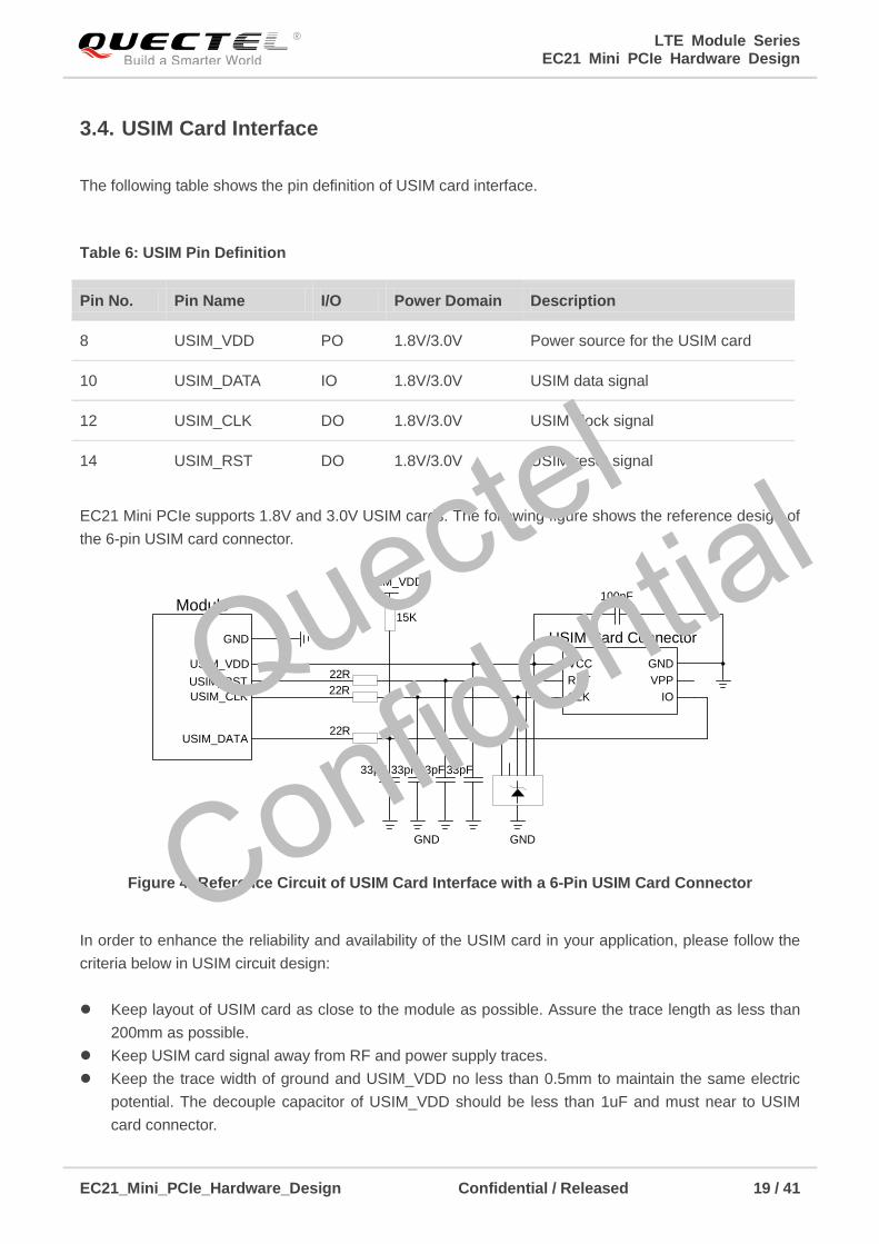
Table 6: USIM Pin Definition
EC21 Mini PCIe supports 1.8V and 3.0V USIM cards. The following figure shows the reference design of
the 6-pin USIM card connector.
USIM_VDD
GND
USIM_RST
USIM_CLK
USIM_DATA22R
22R
22R
100nF
USIM Card Connector
GND
33pF 33pF33pF
VCC
RST
CLK IO
VPP
GND
GND
33pF
15KModule
USIM_VDD
Figure 4: Reference Circuit of USIM Card Interface with a 6-Pin USIM Card Connector
In order to enhance the reliability and availability of the USIM card in your application, please follow the
criteria below in USIM circuit design:
Keep layout of USIM card as close to the module as possible. Assure the trace length as less than
200mm as possible.
Keep USIM card signal away from RF and power supply traces.
Keep the trace width of ground and USIM_VDD no less than 0.5mm to maintain the same electric
potential. The decouple capacitor of USIM_VDD should be less than 1uF and must near to USIM
card connector.
Pin No. Pin Name I/O Power Domain Description
8 USIM_VDD PO 1.8V/3.0V Power source for the USIM card
10 USIM_DATA IO 1.8V/3.0V USIM data signal
12 USIM_CLK DO 1.8V/3.0V USIM clock signal
14 USIM_RST DO 1.8V/3.0V USIM reset signal
Quectel
Confidential

LTE Module Series EC21 Mini PCIe Hardware Design
EC21_Mini_PCIe_Hardware_Design Confidential / Released 20 / 41
To avoid cross-talk between USIM_DATA and USIM_CLK, keep them away from each other and
shield them with surrounding ground.
In order to offer good ESD protection, it is recommended to add a TVS whose parasitic capacitance
should not be more than 50pF. The 22 ohm resistors should be added in series between the module
and USIM card so as to suppress EMI spurious transmission and enhance ESD protection. The 33pF
capacitors are used for filtering interference of GSM900. Please note that the USIM peripheral circuit
should be close to the USIM card connector.
The pull-up resistor on USIM_DATA line can improve anti-jamming capability when long layout trace
and sensitive occasion are applied, and should be placed close to the USIM card connector.
3.5. USB Interface
The following table shows the pin definition of USB interface.
Table 7: Pin Definition of USB Interface
EC21 Mini PCIe is compliant with USB 2.0 specification. It can only be used as a slave device. Meanwhile,
it supports high speed (480Mbps) and full speed (12Mbps) mode. The USB interface is used for AT
command communication, data transmission, GNSS NMEA output, software debugging, firmware
upgrade and voice over USB*. The following figure shows the reference circuit of USB interface.
USB_DP
USB_DM
GND
USB_DP
USB_DM
GND
R1
R2
Close to Module
R3
R4
Test Points
ESD Array
NM_0R
NM_0R
0R
0R
Minimize this stub
Module MCU
Figure 5: Reference Circuit of USB Interface
Pin No. Pin Name I/O Description Comment
36 USB_DM IO USB differential data (-) Require differential impedance of 90Ω
38 USB_DP IO USB differential data (+) Require differential impedance of 90Ω Quectel
Confidential

LTE Module Series EC21 Mini PCIe Hardware Design
EC21_Mini_PCIe_Hardware_Design Confidential / Released 21 / 41
In order to ensure the integrity of USB data line signal, components R1, R2, R3 and R4 must be placed
close to the module, and also these resistors should be placed close to each other. The extra stubs of
trace must be as short as possible.
In order to ensure the USB interface design corresponding with the USB 2.0 specification, please comply
with the following principles:
It is important to route the USB signal traces as differential pairs with total grounding. The impedance
of USB differential trace is 90 ohm.
Do not route signal traces under crystals, oscillators, magnetic devices and RF signal traces. It is
important to route the USB differential traces in inner-layer with ground shielding on not only upper
and lower layers but also right and left sides.
If USB connector is used, please keep the ESD protection components to the USB connector as
close as possible. Pay attention to the influence of junction capacitance of ESD protection
components on USB data lines. Typically, the capacitance value should be less than 2pF.
Keep the ESD components as close as possible to the connector.
Keep traces of USB data test points short to avoid noise coupled on USB data lines. If possible,
reserve a 0R resistor on these two lines.
1. There are three preconditions when enabling EC21 Mini PCIe to enter into the sleep mode:
a) Execute AT+QSCLK=1 command to enable the sleep mode. Please refer to document [2] for
details.
b) DTR pin should be kept in high level (pull-up internally).
c) USB interface on Mini PCIe must be connected with the USB interface of the host and please
guarantee the USB of the host is in suspended state.
2. “*” means under development.
3.6. UART Interface
The following table shows the pin definition of the UART interface.
Table 8: Pin Definition of the UART Interface
Pin No. EC21 Mini PCIe Pin Name I/O Power Domain Description
11 UART_RX DI 3.3V UART receive data
13 UART_TX DO 3.3V UART transmit data
NOTES
Quectel
Confidential

LTE Module Series EC21 Mini PCIe Hardware Design
EC21_Mini_PCIe_Hardware_Design Confidential / Released 22 / 41
The UART interface supports 9600, 19200, 38400, 57600, 115200 and 230400bps baud rate. The default
is 115200bps. This interface can be used for AT command communication.
AT+IPR command can be used to set the baud rate of the UART, and AT+IFC command can be used to
set the hardware flow control (hardware flow control is disabled by default). Please refer to document [2]
for details.
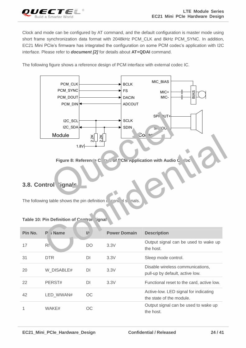
3.7. PCM and I2C Interfaces
The following table shows the pin definition of PCM and 12C interfaces that can be applied in audio codec
design.
Table 9: Pin Definition of PCM and I2C Interfaces
EC21 Mini PCIe provides one PCM digital interface, which supports 8-bit A-law* and μ-law*, and also
supports 16-bit linear data formats and the following modes:
Primary mode (short frame synchronization, works as either master or slave)
Auxiliary mode (long frame synchronization, works as master only)
23 UART_CTS DI 3.3V UART clear to send
25 UART_RTS DO 3.3V UART request to send
Pin No. Pin Name I/O Power Domain Description
45 PCM_CLK IO 1.8V PCM clock signal
47 PCM_DOUT DO 1.8V PCM data output
49 PCM_DIN DI 1.8V PCM data input
51 PCM_SYNC IO 1.8V PCM frame synchronization
30 I2C_SCL DO 1.8V I2C serial clock, require external
pull-up to 1.8V.
32 I2C_SDA IO 1.8V I2C serial data, require external
pull-up to 1.8V.
NOTE
Quectel
Confidential

LTE Module Series EC21 Mini PCIe Hardware Design
EC21_Mini_PCIe_Hardware_Design Confidential / Released 23 / 41
“*” means under development.
In primary mode, the data is sampled on the falling edge of the PCM_CLK and transmitted on the rising
edge. The PCM_SYNC falling edge represents the MSB. In this mode, PCM_CLK supports 128kHz,
256kHz, 512kHz, 1024kHz and 2048kHz. The following figure shows timing relationship in primary mode
with 8kHz PCM_SYNC and 2048kHz PCM_CLK.
PCM_CLK
PCM_SYNC
PCM_DOUT
MSB LSB MSB
125us
1 2 256255
PCM_IN
MSBLSBMSB
Figure 6: Timing in Primary Mode
In auxiliary mode, the data is sampled on the falling edge of the PCM_CLK and transmitted on the rising
edge; while the PCM_SYNC rising edge represents the MSB. In this mode, PCM interface operates with a
128kHz PCM_CLK and an 8kHz, 50% duty cycle PCM_SYNC only. The following figure shows the timing
relationship in auxiliary mode with 8kHz PCM_SYNC and 128kHz PCM_CLK.
PCM_CLK
PCM_SYNC
PCM_DOUT
MSB LSB
PCM_IN
125us
MSB
1 2 1615
LSB
Figure 7: Timing in Auxiliary Mode
NOTE
Quectel
Confidential
LTE Module Series EC21 Mini PCIe Hardware Design
EC21_Mini_PCIe_Hardware_Design Confidential / Released 24 / 41
Clock and mode can be configured by AT command, and the default configuration is master mode using
short frame synchronization data format with 2048kHz PCM_CLK and 8kHz PCM_SYNC. In addition,
EC21 Mini PCIe’s firmware has integrated the configuration on some PCM codec’s application with I2C
interface. Please refer to document [2] for details about AT+QDAI command.
The following figure shows a reference design of PCM interface with external codec IC.
PCM_DIN
PCM_DOUT
PCM_SYNC
PCM_CLK
I2C_SCL
I2C_SDA
CodecModule
1.8V
2.2
K
2.2
K
BCLK
FS
DACIN
ADCOUT
SCLK
SDIN
BIA
S
MIC_BIAS
MIC+
MIC-
SPKOUT+
SPKOUT-
Figure 8: Reference Circuit of PCM Application with Audio Codec
3.8. Control Signals
The following table shows the pin definition of control signals.
Table 10: Pin Definition of Control Signal
Pin No. Pin Name I/O Power Domain Description
17 RI DO 3.3V Output signal can be used to wake up
the host.
31 DTR DI 3.3V Sleep mode control.
20 W_DISABLE# DI 3.3V Disable wireless communications,
pull-up by default, active low.
22 PERST# DI 3.3V Functional reset to the card, active low.
42 LED_WWAN# OC Active-low. LED signal for indicating
the state of the module.
1 WAKE# OC Output signal can be used to wake up
the host.
Quectel
Confidential

LTE Module Series EC21 Mini PCIe Hardware Design
EC21_Mini_PCIe_Hardware_Design Confidential / Released 25 / 41
3.8.1. RI Signal
The RI signal can be used to wake up the host. When URC returns, there will be the following behavior on
the RI pin after executing AT+QCFG=“risignaltype”,“physical” command.
URC return
120 msHigh
Low
Figure 9: RI Behavior
3.8.2. DTR Signal
The DTR signal supports sleep control function. Driving it to low level will wake up the module.
3.8.3. W_DISABLE# Signal
EC21 Mini PCIe provides W_DISABLE# signal to disable wireless communications through hardware
operation. The following table shows the radio operational states of the module. Please refer to
document [2] for related AT commands.
Table 11: Radio Operational States
3.8.4. PERST# Signal
The PERST# signal can be used to force a hardware reset on the card. You can reset the module by
driving the PERST# to a low level voltage within the time frame of 150~460ms and then releasing it. The
reset scenario is illustrated in the following figure.
W_DISABLE# AT Commands Radio Operation
High Level AT+CFUN=1 Enabled
High Level AT+CFUN=0
AT+CFUN=4 Disabled
Low Level
AT+CFUN=0
AT+CFUN=1
AT+CFUN=4
Disabled
Quectel
Confidential

LTE Module Series EC21 Mini PCIe Hardware Design
EC21_Mini_PCIe_Hardware_Design Confidential / Released 26 / 41
VIL≤0.5V
VIH≥2.3V
VCC_3V3
≥150ms
ResettingModule
StatusRunning
PERST#
Restart
≤460ms
Figure 10: Timing of Resetting Module
3.8.5. LED_WWAN# Signal
The LED_WWAN# signal of EC21 Mini PCIe is used to indicate the network status of the module, which
can absorb the current up to 40mA. According to the following circuit, in order to reduce the current of the
LED, a resistor must be placed in series with the LED. The LED is emitting light when the LED_WWAN#
output signal is active low.
LED_WWAN#VCC
R
Figure 11: LED_WWAN# Signal Reference Circuit Diagram
The following table shows the network status indications of the LED_WWAN# signal.
Table 12: Indications of Network Status
LED_WWAN# Description
Low Level (Light on) Registered on network
High-impedance (Light off)
No network coverage or not registered
W_DISABLE# signal is at low level. (Disable the RF)
AT+CFUN=0, AT+CFUN=4
Quectel
Confidential

LTE Module Series EC21 Mini PCIe Hardware Design
EC21_Mini_PCIe_Hardware_Design Confidential / Released 27 / 41
3.8.6. WAKE# Signal
The WAKE# signal is an open collector signal which is similar to RI signal, but a host pull-up resistor and
AT+QCFG=“risignaltype”,“physical” command are required. When URC returns, there will be 120ms
low level pulse output as below.
URC return
120 msHigh
Low
(external
pull-up)
Figure 12: WAKE# Behavior
3.9. Antenna Interfaces
EC21 Mini PCIe antenna interfaces include a main antenna interface, a Rx-diversity antenna interface
and a GNSS antenna interface. And Rx-diversity function is enabled by default.
The following table shows the requirement on main antenna, Rx-diversity antenna and GNSS antenna.
Table 13: Antenna Requirements
Type Requirements
GNSS
Frequency range: 1561~1615MHz
Polarization: RHCP or linear
VSWR: <2 (Typ.)
Passive antenna gain: >0dBi
GSM/WCDMA/LTE
VSWR: ≤2
Gain (dBi): 1
Max Input Power (W): 50
Input Impedance (ohm): 50
Polarization Type: Vertical
Cable Insertion Loss: <1dB
(GSM900, WCDMA B5/B8, LTE B5/B8/B12/B13/B20/B28)
Cable Insertion Loss: <1.5dB
(GSM1800, WCDMA B1/B2, LTE B1/B2/B3/B4)
Cable insertion loss <2dB
(LTE B7)
Quectel
Confidential

LTE Module Series EC21 Mini PCIe Hardware Design
EC21_Mini_PCIe_Hardware_Design Confidential / Released 28 / 41
The following figure shows the overall sizes of RF connector.
Figure 13: Dimensions of the RF Connector (Unit: mm)
U.FL-LP serial connectors listed in the following figure can be used to match the RF connector.
Figure 14: Mechanicals of UF.L-LP Connectors
Quectel
Confidential

LTE Module Series EC21 Mini PCIe Hardware Design
EC21_Mini_PCIe_Hardware_Design Confidential / Released 29 / 41
4 Electrical and Radio Characteristics
4.1. General Description
This chapter mainly describes the following electrical and radio characteristics of EC21 Mini PCIe:
Power supply requirements
I/O requirements
Current consumption
RF characteristics
GNSS receiver
ESD characteristics
4.2. Power Supply Requirements
The input voltage of EC21 Mini PCIe is 3.3V±9%, as specified by PCI Express Mini CEM Specifications
1.2. The following table shows the power supply requirements of EC21 Mini PCIe.
Table 14: Power Supply Requirements
Parameter Description Min. Typ. Max. Unit
VCC_3V3 Power Supply 3.0 3.3 3.6 V
Quectel
Confidential

LTE Module Series EC21 Mini PCIe Hardware Design
EC21_Mini_PCIe_Hardware_Design Confidential / Released 30 / 41
4.3. I/O Requirements
The following table shows the I/O requirements of EC21 Mini PCIe.
Table 15: I/O Requirements
1. The PCM and I2C interfaces belong to 1.8V power domain and other I/O interfaces belong to
VCC_3V3 power domain.
2. The maximum voltage value of VIL for PERST# signal and W_DISABLE# signal is 0.5V.
4.4. RF Characteristics
The following tables show conducted RF output power and receiving sensitivity of EC21 Mini PCIe
module.
Table 16: EC21 Mini PCIe Conducted RF Output Power
Parameter Description Min. Max. Unit
VIH Input High Voltage 0.7 × VCC_3V3 VCC_3V3+0.3 V
VIL Input Low Voltage -0.3 0.3 × VCC_3V3 V
VOH Output High Voltage VCC_3V3-0.5 VCC_3V3 V
VOL Output Low Voltage 0 0.4 V
Frequency Max. Min.
GSM850/GSM900 33dBm±2dB 5dBm±5dB
DCS1800/PCS1900 30dBm±2dB 0dBm±5dB
GSM850/GSM900 (8-PSK) 27dBm±3dB 5dBm±5dB
DCS1800/PCS1900 (8-PSK) 26dBm±3dB 0dBm±5dB
WCDMA bands 24dBm+1/-3dB <-50dBm
LTE-FDD bands 23dBm±2dB <-44dBm
NOTES
Quectel
Confidential
LTE Module Series EC21 Mini PCIe Hardware Design
EC21_Mini_PCIe_Hardware_Design Confidential / Released 31 / 41
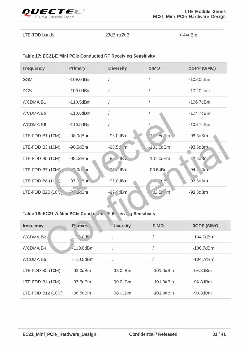
Table 17: EC21-E Mini PCIe Conducted RF Receiving Sensitivity
Frequency Primary Diversity SIMO 3GPP (SIMO)
GSM -109.0dBm / / -102.0dBm
DCS -109.0dBm / / -102.0dbm
WCDMA B1 -110.5dBm / / -106.7dBm
WCDMA B5 -110.5dBm / / -104.7dBm
WCDMA B8 -110.5dBm / / -103.7dBm
LTE-FDD B1 (10M) -98.0dBm -98.0dBm -101.5dBm -96.3dBm
LTE-FDD B3 (10M) -96.5dBm -98.5dBm -101.5dBm -93.3dBm
LTE-FDD B5 (10M) -98.0dBm -98.5dBm -101.0dBm -94.3dBm
LTE-FDD B7 (10M) -97.0dBm -94.5dBm -99.5dBm -94.3dBm
LTE-FDD B8 (10M) -97.0dBm -97.0dBm -101.0dBm -93.3dBm
LTE-FDD B20 (10M) -97.5dBm -99.0dBm -102.5dBm -93.3dBm
Table 18: EC21-A Mini PCIe Conducted RF Receiving Sensitivity
frequency Primary Diversity SIMO 3GPP (SIMO)
WCDMA B2 -110.0dBm / / -104.7dBm
WCDMA B4 -110.0dBm / / -106.7dBm
WCDMA B5 -110.5dBm / / -104.7dBm
LTE-FDD B2 (10M) -98.0dBm -98.0dBm -101.0dBm -94.3dBm
LTE-FDD B4 (10M) -97.5dBm -99.0dBm -101.0dBm -96.3dBm
LTE-FDD B12 (10M) -96.5dBm -98.0dBm -101.0dBm -93.3dBm
LTE-TDD bands 23dBm±2dB <-44dBm
Quectel
Confidential

LTE Module Series EC21 Mini PCIe Hardware Design
EC21_Mini_PCIe_Hardware_Design Confidential / Released 32 / 41
Table 19: EC21-V Mini PCIe Conducted RF Receiving Sensitivity
Frequency Primary Diversity SIMO 3GPP (SIMO)
LTE-FDD B4 (10M) -97.5dBm -99.0dBm -101.0dBm -96.3dBm
LTE-FDD B13 (10M) -95.0dBm -97.0dBm -100.0dBm -93.3dBm
Table 20: EC21-AUT Mini PCIe Conducted RF Receiving Sensitivity
Frequency Primary Diversity SIMO 3GPP (SIMO)
WCDMA B1 -110.0dBm / / -106.7dBm
WCDMA B5 -110.5dBm / / -104.7dBm
LTE-FDD B1 (10M) -98.5dBm -98.0dBm -101.0dBm -96.3dBm
LTE-FDD B3 (10M) -98.0dBm -96.0dBm -100.0dBm -93.3dBm
LTE-FDD B5 (10M) -98.0dBm -99.0dBm -102.5dBm -94.3dBm
LTE-FDD B7 (10M) -97.0dBm -95.0dBm -98.5dBm -94.3dBm
LTE-FDD B28 (10M) -97.0dBm -99.0dBm -102.0dBm -94.8dBm
Table 21: EC21-KL Mini PCIe Conducted RF Receiving Sensitivity
Frequency Primary Diversity SIMO 3GPP (SIMO)
LTE-FDD B1 (10M) -98.0dBm -99.5dBm -100.5dBm -96.3dBm
LTE-FDD B3 (10M) -97.0dBm -97.5dBm -99.5dBm -93.3dBm
LTE-FDD B5 (10M) -98.0dBm -99.5dBm -100.5dBm -94.3dBm
LTE-FDD B7 (10M) -96.0dBm -96.0dBm -98.5dBm -94.3dBm
LTE-FDD B8 (10M) -97.0dBm -99.0dBm -101.0dBm -93.3dBm
Quectel
Confidential

LTE Module Series EC21 Mini PCIe Hardware Design
EC21_Mini_PCIe_Hardware_Design Confidential / Released 33 / 41
Table 22: EC21-J Mini PCIe Conducted RF Receiving Sensitivity
4.5. GNSS Receiver
EC21 Mini PCIe integrates a GNSS receiver that supports Gen8C Lite of Qualcomm (GPS, GLONASS,
BeiDou, Galileo and QZSS). Meanwhile, it supports Qualcomm gpsOneXTRA technology (one kind of
A-GNSS). This technology will download XTRA file from the internet server to enhance the TTFF. XTRA
file contains predicted GPS and GLONASS satellites coordinates and clock biases valid for up to 7 days.
It is best if XTRA file is downloaded every 1-2 days. Additionally, EC21 Mini PCIe can support standard
NMEA-0183 protocol and output NMEA messages with 1Hz via USB NMEA interface.
EC21 Mini PCIe GNSS engine is switched off by default. You must switch on it by AT command. Please
refer to document [3] for more details about GNSS engine technology and configurations. A passive
antenna should be used for the GNSS engine.
4.6. ESD Characteristics
The following table shows the ESD characteristics of EC21 Mini PCIe.
Table 23: ESD Characteristics of EC21 Mini PCIe
Frequency Primary Diversity SIMO 3GPP (SIMO)
LTE-FDD B1 (10M) -97.5dBm -98.7dBm -100.2dBm -96.3dBm
LTE-FDD B3 (10M) -96.5dBm -97.1dBm -100.5dBm -93.3dBm
LTE-FDD B8 (10M) -98.4dBm -99.0dBm -101.2dBm -93.3dBm
LTE-FDD B18 (10M) -99.5dBm -99.0dBm -101.7dBm -96.3dBm
LTE-FDD B19 (10M) -99.2dBm -99.0dBm -101.4dBm -96.3dBm
LTE-FDD B26 (10M) -99.5dBm -99.0dBm -101.5dBm -93.8dBm
Part Contact Discharge Air Discharge Unit
Power Supply and GND +/-5 +/-10 kV
Antenna Interface +/-4 +/-8 kV
Quectel
Confidential

LTE Module Series EC21 Mini PCIe Hardware Design
EC21_Mini_PCIe_Hardware_Design Confidential / Released 34 / 41
4.7. Current Consumption
The following tables describe the current consumption of EC21 Mini PCIe series module.
Table 24: Current Consumption of EC21-A Mini PCIe
Parameter Description Conditions Typ. Unit
IVBAT
Sleep state
AT+CFUN=0 (USB disconnected) 3.5 mA
WCDMA PF=64 (USB disconnected) 5.0 mA
WCDMA PF=128 (USB disconnected) 4.4 mA
LTE-FDD PF=64 (USB disconnected) 5.3 mA
LTE-FDD PF=128 (USB disconnected) 4.5 mA
Idle state
WCDMA PF=64 (USB disconnected) 32.0 mA
WCDMA PF=64 (USB connected) 45.0 mA
LTE-FDD PF=64 (USB disconnected) 32.0 mA
LTE-FDD PF=64 (USB connected) 45.0 mA
WCDMA data
transfer
(GNSS OFF)
WCDMA B2 HSDPA @21.59dBm 582.0 mA
WCDMA B2 HSUPA @22.17dBm 675.0 mA
WCDMA B4 HSDPA @21.47dBm 575.0 mA
WCDMA B4 HSUPA @21.73dBm 637.0 mA
WCDMA B5 HSDPA @20.02dBm 686.0 mA
WCDMA B5 HSUPA @20.18dBm 577.0 mA
LTE data
transfer
(GNSS OFF)
LTE-FDD B2 @22.93dBm 926.0 mA
LTE-FDD B4 @22.72dBm 934.0 mA
USB Interface +/-4 +/-8 kV
USIM Interface +/-4 +/-8 kV
Others +/-0.5 +/-1 kV
Quectel
Confidential

LTE Module Series EC21 Mini PCIe Hardware Design
EC21_Mini_PCIe_Hardware_Design Confidential / Released 35 / 41
LTE-FDD B12 @23.26dBm 835.0 mA
WCDMA
voice call
WCDMA B2 @22.88dBm 610.0 mA
WCDMA B4 @23.21dBm 743.0 mA
WCDMA B5 @23.13dBm 643.0 mA
Table 25: Current Consumption of EC21-V Mini PCIe
Parameter Description Conditions Typ. Unit
IVBAT
Sleep state
AT+CFUN=0 (USB disconnected) 3.8 mA
LTE-FDD PF=64 (USB disconnected) 5.3 mA
LTE-FDD PF=128 (USB disconnected) 4.9 mA
Idle state
LTE-FDD PF=64 (USB disconnected) 30.0 mA
LTE-FDD PF=64 (USB connected) 42.0 mA
LTE data
transfer
(GNSS OFF)
LTE-FDD B4 @23.59dBm 997.0 mA
LTE-FDD B13 @24.05dBm 724.0 mA
Table 26: Current Consumption of EC21-KL Mini PCIe
Parameter Description Conditions Typ. Unit
IVBAT
Sleep state
AT+CFUN=0 (USB disconnected) 3.5 mA
LTE-FDD PF=64 (USB disconnected) 5.6 mA
LTE-FDD PF=128 (USB disconnected) 4.7 mA
Idle state
LTE-FDD PF=64 (USB disconnected) 35.0 mA
LTE-FDD PF=64 (USB connected) 49.0 mA
LTE data
transfer
(GNSS OFF)
LTE-FDD B1 @22.78dBm 972.0 mA
LTE-FDD B3 @23.03dBm 974.0 mA
LTE-FDD B5 @23.03dBm 764.0 mA
LTE-FDD B7 @22.89dBm 959.0 mA
Quectel
Confidential
LTE Module Series EC21 Mini PCIe Hardware Design
EC21_Mini_PCIe_Hardware_Design Confidential / Released 36 / 41
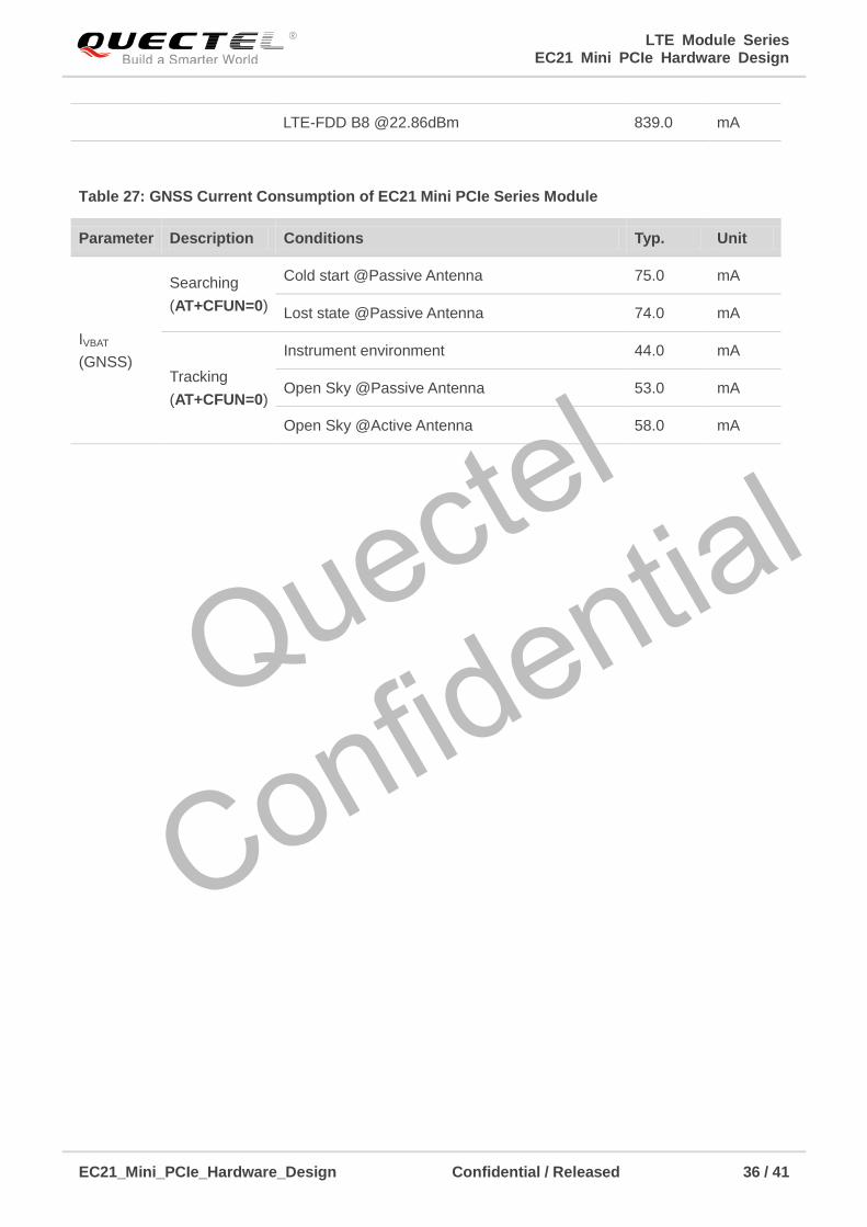
LTE-FDD B8 @22.86dBm 839.0 mA
Table 27: GNSS Current Consumption of EC21 Mini PCIe Series Module
Parameter Description Conditions Typ. Unit
IVBAT
(GNSS)
Searching
(AT+CFUN=0)
Cold start @Passive Antenna 75.0 mA
Lost state @Passive Antenna 74.0 mA
Tracking
(AT+CFUN=0)
Instrument environment 44.0 mA
Open Sky @Passive Antenna 53.0 mA
Open Sky @Active Antenna 58.0 mA
Quectel
Confidential
LTE Module Series EC21 Mini PCIe Hardware Design
EC21_Mini_PCIe_Hardware_Design Confidential / Released 37 / 41
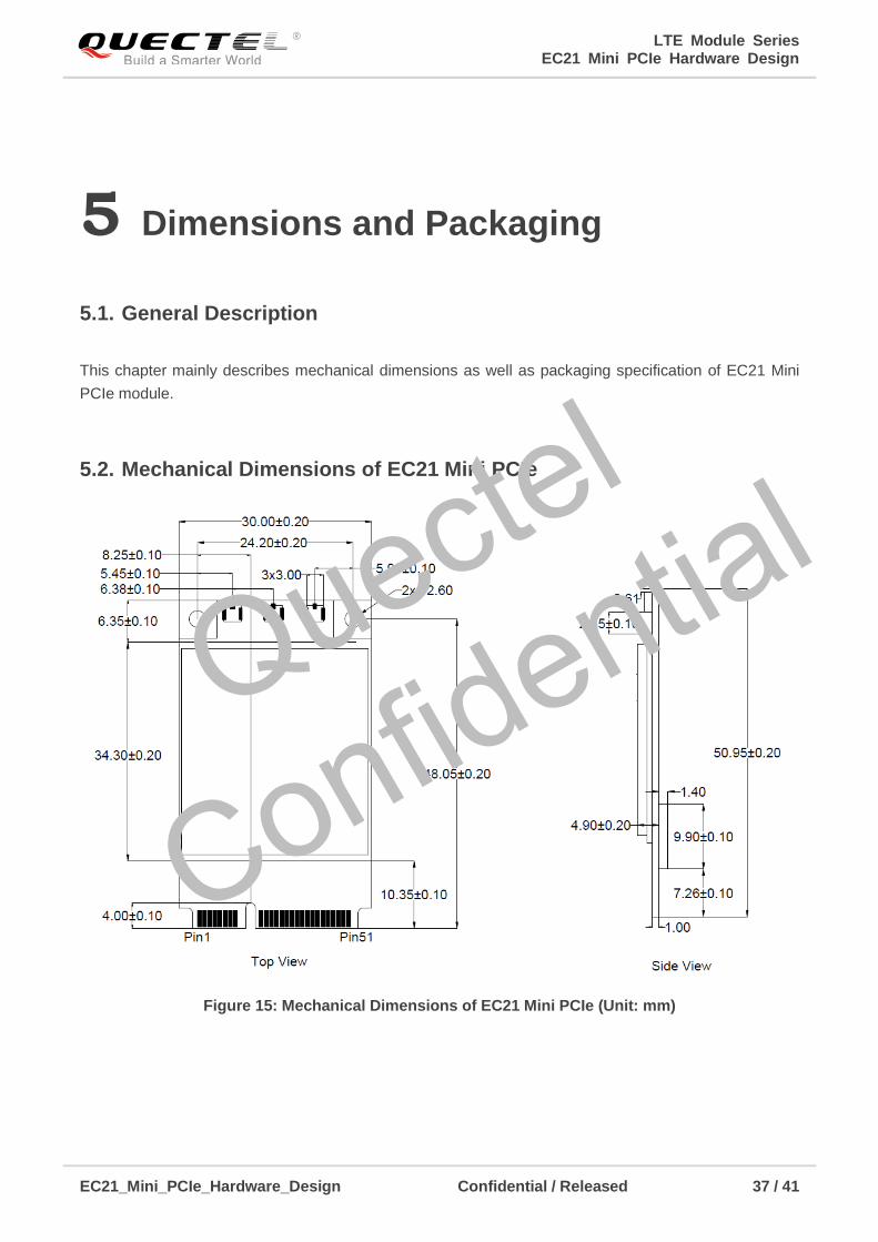
5 Dimensions and Packaging
5.1. General Description
This chapter mainly describes mechanical dimensions as well as packaging specification of EC21 Mini
PCIe module.
5.2. Mechanical Dimensions of EC21 Mini PCIe
Figure 15: Mechanical Dimensions of EC21 Mini PCIe (Unit: mm)
Quectel
Confidential

LTE Module Series EC21 Mini PCIe Hardware Design
EC21_Mini_PCIe_Hardware_Design Confidential / Released 38 / 41
5.3. Standard Dimensions of Mini PCI Express
The following figure shows the standard dimensions of Mini PCI Express. Please refer to document [1]
for detailed A and B.
Figure 16: Standard Dimensions of Mini PCI Express (Unit: mm)
Quectel
Confidential

LTE Module Series EC21 Mini PCIe Hardware Design
EC21_Mini_PCIe_Hardware_Design Confidential / Released 39 / 41
EC21 Mini PCIe adopts a standard Mini PCI Express connector which compiles with the directives and
standards listed in the document [1]. The following figure takes the Molex 679100002 as an example.
Figure 17: Dimensions of the Mini PCI Express Connector (the Molex 679100002, Unit: mm)
5.4. Packaging Specification
The EC21 Mini PCIe is packaged in tray. Each tray contains 10pcs of modules. The smallest package of
EC21 Mini PCIe contains 100pcs.
Quectel
Confidential

LTE Module Series EC21 Mini PCIe Hardware Design
EC21_Mini_PCIe_Hardware_Design Confidential / Released 40 / 41
6 Appendix References
Table 28: Related Documents
Table 29: Terms and Abbreviations
SN Document Name Remark
[1] PCI Express Mini Card Electromechanical
Specification Revision 1.2 Mini PCI Express Specification
[2] Quectel_EC25&EC21_AT_Commands_Manual EC25 and EC21 AT Commands Manual
[3] Quectel_EC25&EC21_GNSS_AT_Commands_
Manual
EC25 and EC21 GNSS AT Commands
Manual
Abbreviation Description
AMR Adaptive Multi-rate
bps Bits Per Second
CS Coding Scheme
DC-HSPA+ Dual-carrier High Speed Packet Access
DFOTA Delta Firmware Upgrade Over The Air
DL Down Link
EFR Enhanced Full Rate
ESD Electrostatic Discharge
FDD Frequency Division Duplexing
FR Full Rate
GLONASS GLObalnaya Navigatsionnaya Sputnikovaya Sistema, the Russian Global
Navigation Satellite System
GMSK Gaussian Minimum Shift Keying
GNSS Global Navigation Satellite System
Quectel
Confidential

LTE Module Series EC21 Mini PCIe Hardware Design
EC21_Mini_PCIe_Hardware_Design Confidential / Released 41 / 41
GPS Global Positioning System
GSM Global System for Mobile Communications
HR Half Rate
HSPA High Speed Packet Access
HSUPA High Speed Uplink Packet Access
kbps Kilo Bits Per Second
LED Light Emitting Diode
LTE Long-Term Evolution
Mbps Million Bits Per Second
ME Mobile Equipment (Module)
MIMO Multiple-Input Multiple-Output
MMS Multimedia Messaging Service
MO Mobile Originated
MT Mobile Terminated
PCM Pulse Code Modulation
PDU Protocol Data Unit
PPP Point-to-Point Protocol
RF Radio Frequency
Rx Receive
USIM Universal Subscriber Identification Module
SMS Short Message Service
UART Universal Asynchronous Receiver & Transmitter
UL Up Link
URC Unsolicited Result Code
WCDMA Wideband Code Division Multiple Access
Quectel
Confidential