Embed Size (px)
Citation preview
EE C245 – ME C218Introduction to MEMS Design
Fall 2007Fall 2007
Prof Clark T C NguyenProf. Clark T.-C. Nguyen
Dept of Electrical Engineering & Computer SciencesDept. of Electrical Engineering & Computer SciencesUniversity of California at Berkeley
Berkeley, CA 94720y
L t 10 S f Mi hi i III / M h i
EE C245: Introduction to MEMS Design Lecture 10 C. Nguyen 9/30/08 1
Lecture 10: Surface Micromachining III / Mechanics of Materials
Lecture Outline
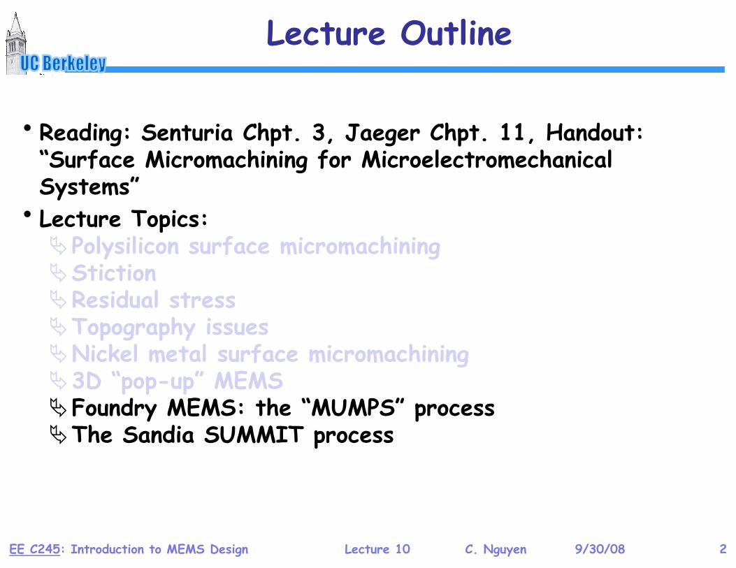
• Reading: Senturia Chpt. 3, Jaeger Chpt. 11, Handout: g p g p“Surface Micromachining for MicroelectromechanicalSystems”
• Lecture Topics:• Lecture Topics:Polysilicon surface micromachiningStictionResidual stressTopography issuesNickel metal surface micromachiningNickel metal surface micromachining3D “pop-up” MEMSFoundry MEMS: the “MUMPS” processThe Sandia SUMMIT process
EE C245: Introduction to MEMS Design Lecture 10 C. Nguyen 9/30/08 2
“Foundry” MEMS:Th MUMPS PThe MUMPS Process
EE C245: Introduction to MEMS Design Lecture 10 C. Nguyen 9/30/08 3

MUMPS: MMultiUUser MEMS PProcesSS
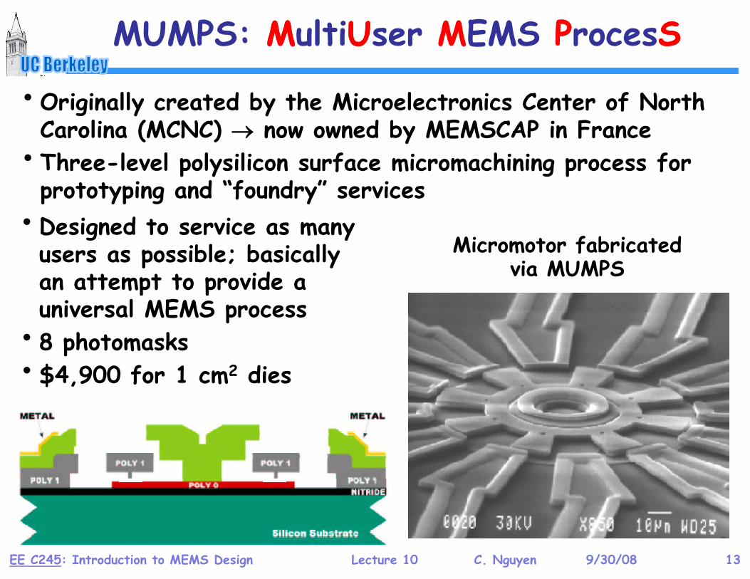
•Originally created by the Microelectronics Center of North Carolina (MCNC) → now owned by MEMSCAP in France
• Three-level polysilicon surface micromachining process for prototyping and “foundry” services
• D i d t i • Designed to service as many users as possible; basically an attempt to provide a
Micromotor fabricated via MUMPSan attempt to prov de a
universal MEMS process• 8 photomasks• $4,900 for 1 cm2 dies
EE C245: Introduction to MEMS Design Lecture 10 C. Nguyen 9/30/08 4
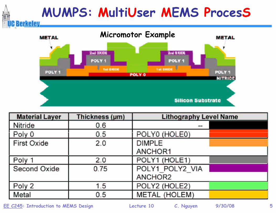
MUMPS: MMultiUUser MEMS PProcesSSMicromotor Example
EE C245: Introduction to MEMS Design Lecture 10 C. Nguyen 9/30/08 5
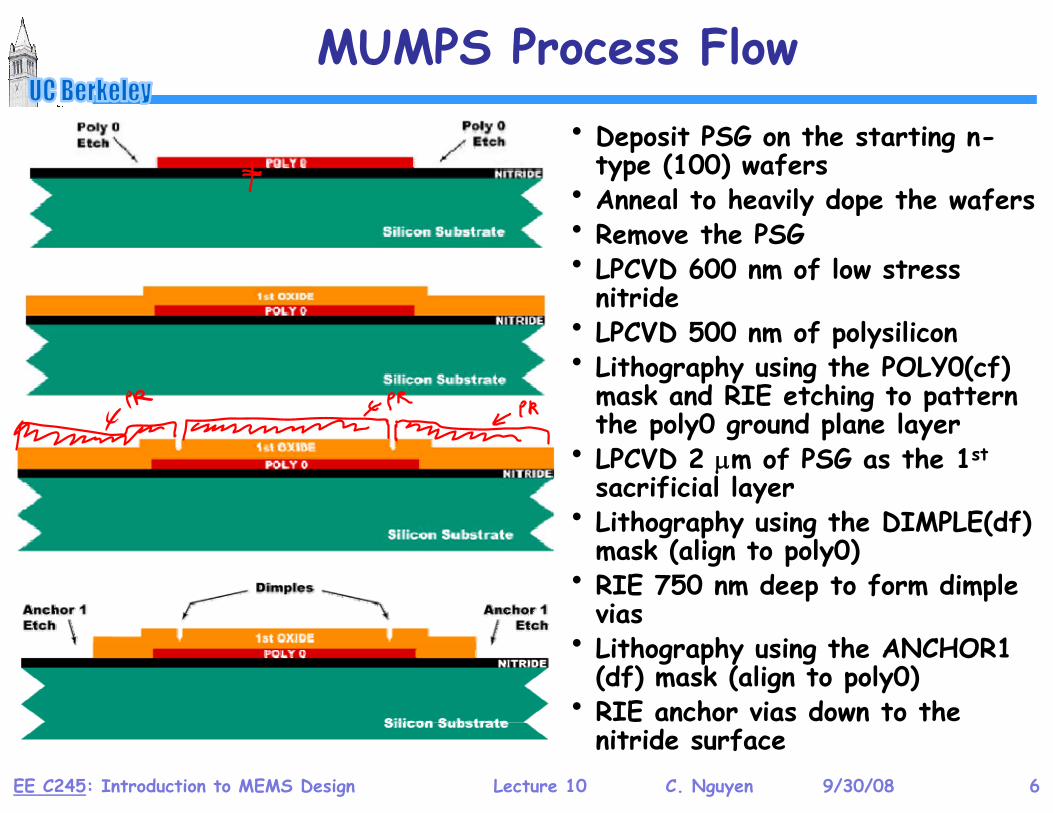
MUMPS Process Flow
• Deposit PSG on the starting n-type (100) wafers
• Anneal to heavily dope the wafersnn a to h a y op th waf rs• Remove the PSG• LPCVD 600 nm of low stress
nitride• LPCVD 500 nm of polysilicon• Lithography using the POLY0(cf)
mask and RIE etching to pattern g pthe poly0 ground plane layer
• LPCVD 2 μm of PSG as the 1st
sacrificial layer• Lithography using the DIMPLE(df)
mask (align to poly0)• RIE 750 nm deep to form dimple
ivias• Lithography using the ANCHOR1
(df) mask (align to poly0)• RIE h i d t th
EE C245: Introduction to MEMS Design Lecture 10 C. Nguyen 9/30/08 6
• RIE anchor vias down to the nitride surface
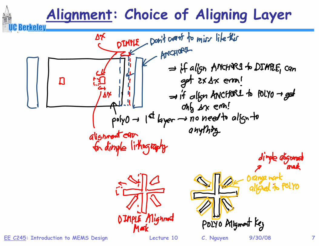
Alignment: Choice of Aligning Layer
EE C245: Introduction to MEMS Design Lecture 10 C. Nguyen 9/30/08 7
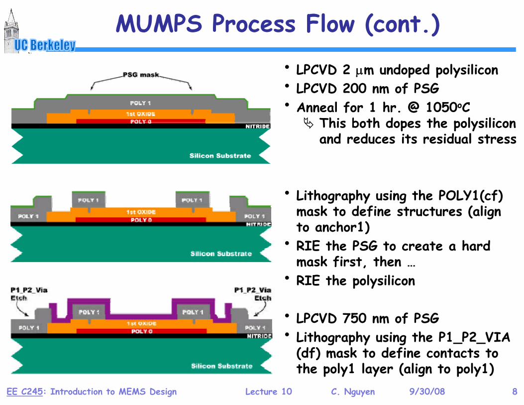
MUMPS Process Flow (cont.)
• LPCVD 2 μm undoped polysilicon• LPCVD 200 nm of PSG• A l f 1 h @ 1050oC• Anneal for 1 hr. @ 1050oC
This both dopes the polysilicon and reduces its residual stress
• Lithography using the POLY1(cf) g p y g ( )mask to define structures (align to anchor1)
• RIE the PSG to create a hard mask first, then …
• RIE the polysilicon
• LPCVD 750 nm of PSG• Lithography using the P1_P2_VIA
(df) k t d fi t t t
EE C245: Introduction to MEMS Design Lecture 10 C. Nguyen 9/30/08 8
(df) mask to define contacts to the poly1 layer (align to poly1)
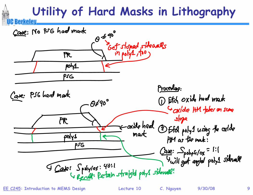
Utility of Hard Masks in Lithography
EE C245: Introduction to MEMS Design Lecture 10 C. Nguyen 9/30/08 9
MUMPS Process Flow (cont.)
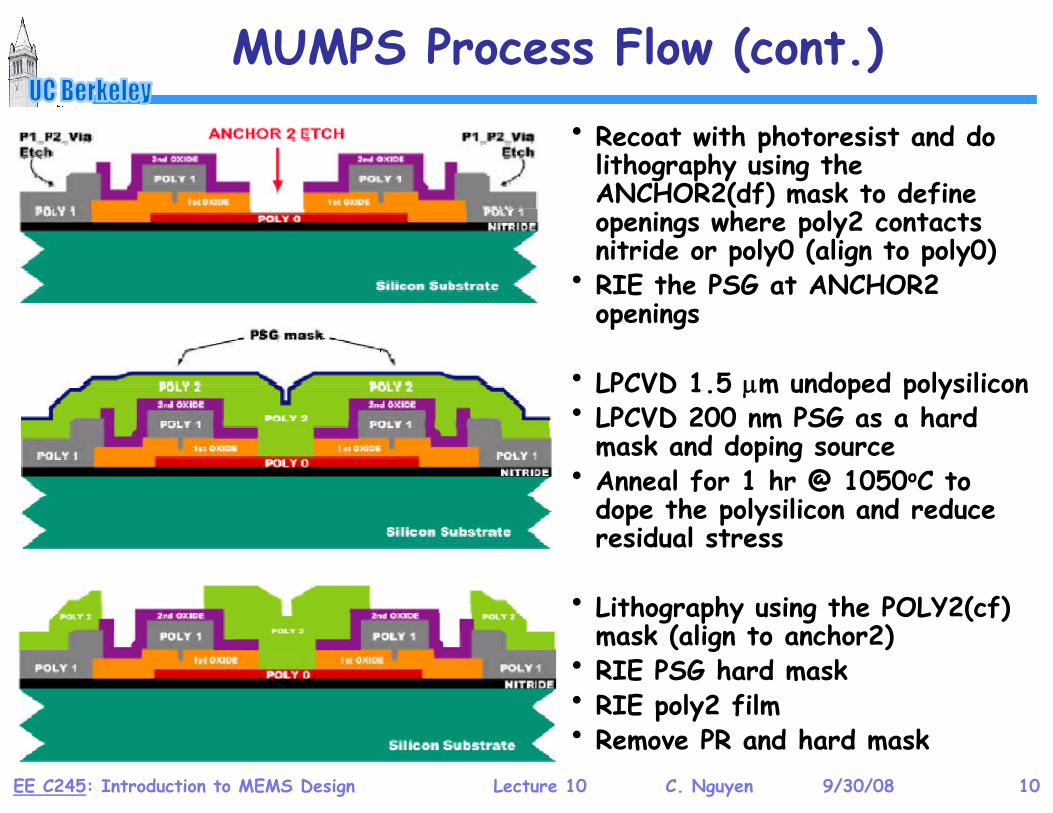
• Recoat with photoresist and do lithography using the ANCHOR2(df) mask to define openings where poly2 contacts nitride or poly0 (align to poly0)
• RIE the PSG at ANCHOR2 iopenings
• LPCVD 1.5 μm undoped polysiliconP D 00 P G h d • LPCVD 200 nm PSG as a hard
mask and doping source• Anneal for 1 hr @ 1050oC to
dope the polysilicon and reduce dope the polysilicon and reduce residual stress
• Lithography using the POLY2(cf) • Lithography using the POLY2(cf) mask (align to anchor2)
• RIE PSG hard mask• RIE poly2 film
EE C245: Introduction to MEMS Design Lecture 10 C. Nguyen 9/30/08 10
• RIE poly2 film• Remove PR and hard mask
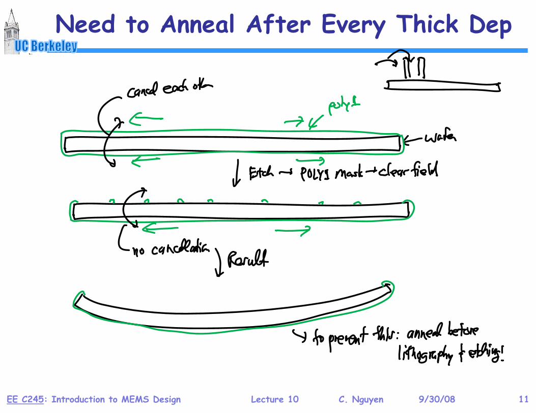
Need to Anneal After Every Thick Dep
EE C245: Introduction to MEMS Design Lecture 10 C. Nguyen 9/30/08 11
MUMPS Process Flow (cont.)
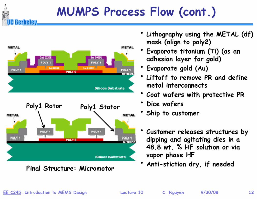
• Lithography using the METAL (df) mask (align to poly2)
• Evaporate titanium (Ti) (as an Evaporate titanium (Ti) (as an adhesion layer for gold)
• Evaporate gold (Au)• Lift ff t PR d d fi • Liftoff to remove PR and define
metal interconnects• Coat wafers with protective PR• Dice wafers• Ship to customer
Poly1 Rotor Poly1 Stator
• Customer releases structures by dipping and agitating dies in a 48 8 wt % HF solution or via 48.8 wt. % HF solution or via vapor phase HF
• Anti-stiction dry, if neededFinal Structure: Micromotor
EE C245: Introduction to MEMS Design Lecture 10 C. Nguyen 9/30/08 12
MUMPS: MMultiUUser MEMS PProcesSS
•Originally created by the Microelectronics Center of North Carolina (MCNC) → now owned by MEMSCAP in France
• Three-level polysilicon surface micromachining process for prototyping and “foundry” services
• D i d t i • Designed to service as many users as possible; basically an attempt to provide a
Micromotor fabricated via MUMPSan attempt to prov de a
universal MEMS process• 8 photomasks• $4,900 for 1 cm2 dies
EE C245: Introduction to MEMS Design Lecture 10 C. Nguyen 9/30/08 13
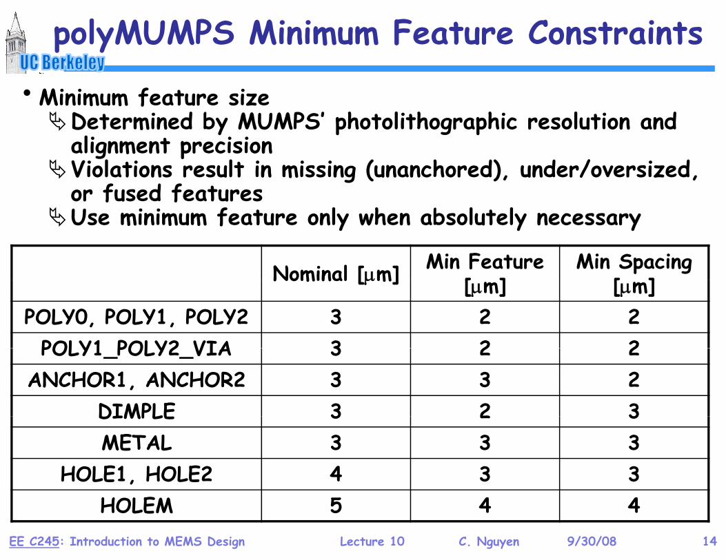
polyMUMPS Minimum Feature Constraints
•Minimum feature sizeDetermined by MUMPS’ photolithographic resolution and alignment precisionalignment precisionViolations result in missing (unanchored), under/oversized, or fused featuresU i i f t l h b l t l Use minimum feature only when absolutely necessary
Nominal [μm] Min Feature [ ]
Min Spacing [ ]Nominal [μm] [μm] [μm]
POLY0, POLY1, POLY2 3 2 2POLY1 POLY2 VIA 3 2 2POLY1_POLY2_VIA 3 2 2
ANCHOR1, ANCHOR2 3 3 2DIMPLE 3 2 3DIMPLE 3 2 3METAL 3 3 3
HOLE1, HOLE2 4 3 3
EE C245: Introduction to MEMS Design Lecture 10 C. Nguyen 9/30/08 14
,HOLEM 5 4 4
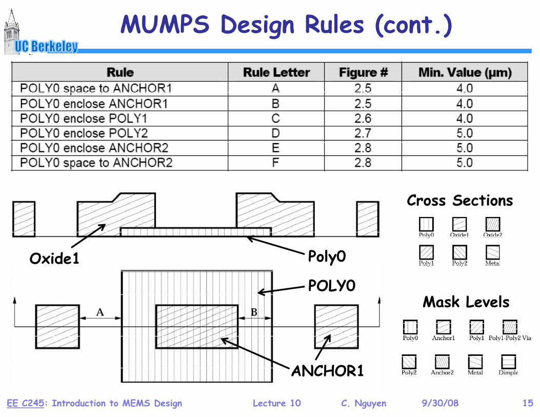
MUMPS Design Rules (cont.)
Cross Sections
Oxide1 Poly0
Mask LevelsPOLY0
Oxide1 Poly0
EE C245: Introduction to MEMS Design Lecture 10 C. Nguyen 9/30/08 15
ANCHOR1
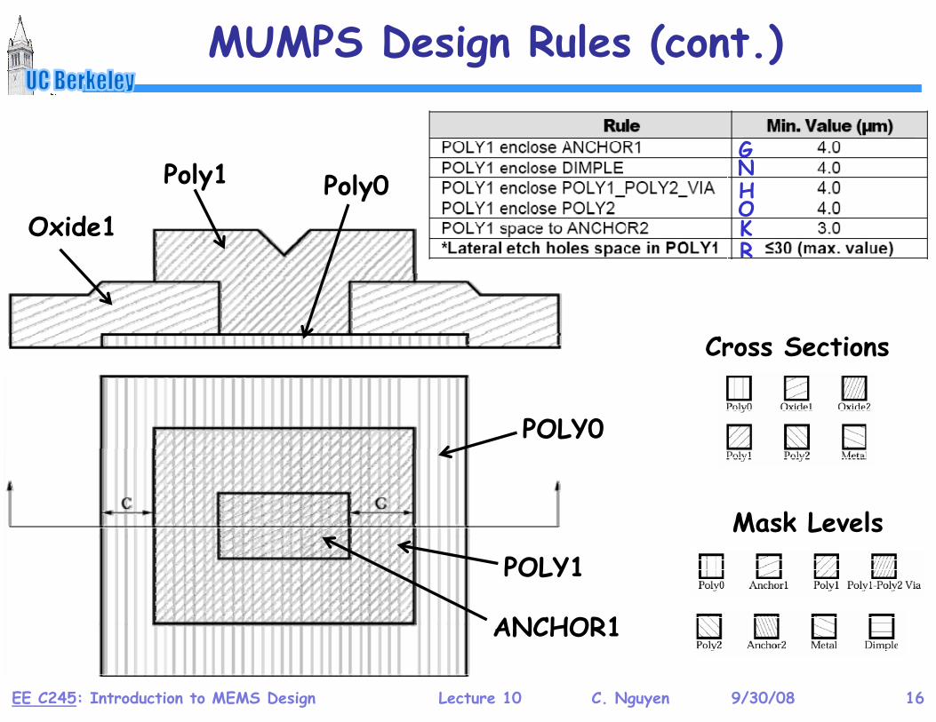
MUMPS Design Rules (cont.)
Poly1 Poly0GNH
y
Oxide1Poly0 H
OKR
Cross Sections
POLY0
Mask Levels
ANCHOR1
POLY1
EE C245: Introduction to MEMS Design Lecture 10 C. Nguyen 9/30/08 16
ANCHOR1
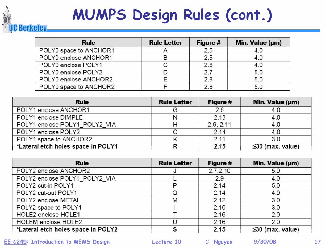
MUMPS Design Rules (cont.)
EE C245: Introduction to MEMS Design Lecture 10 C. Nguyen 9/30/08 17
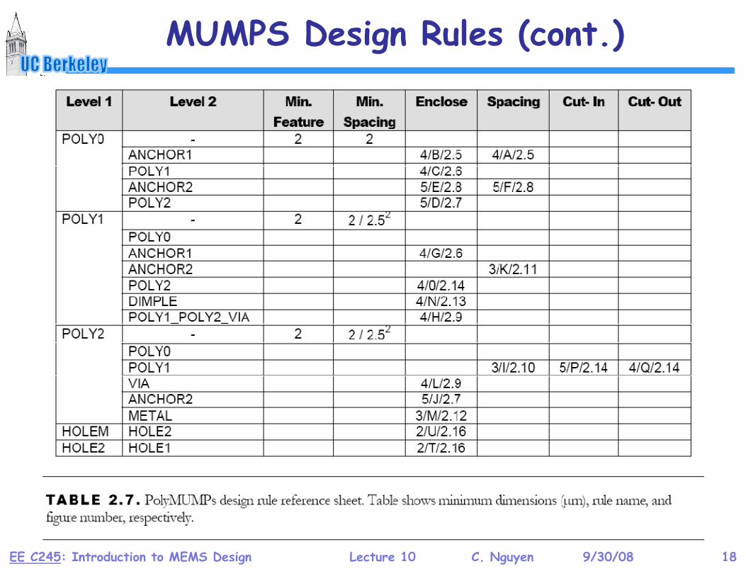
MUMPS Design Rules (cont.)
EE C245: Introduction to MEMS Design Lecture 10 C. Nguyen 9/30/08 18
The Sandia SUMMIT ProcessThe Sandia SUMMIT Process
EE C245: Introduction to MEMS Design Lecture 10 C. Nguyen 9/30/08 19
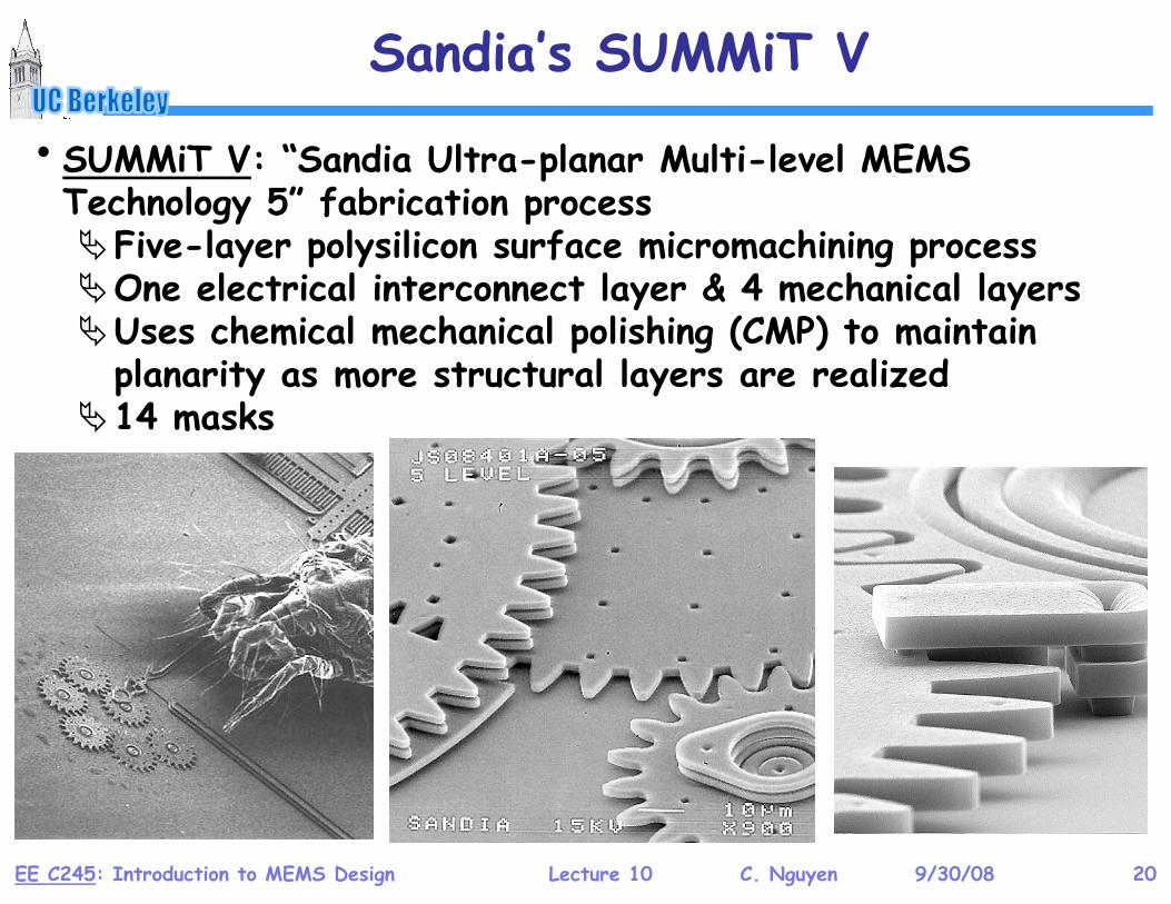
Sandia’s SUMMiT V
• SUMMiT V: “Sandia Ultra-planar Multi-level MEMS Technology 5” fabrication process
Fi l l ili f i hi i Five-layer polysilicon surface micromachining processOne electrical interconnect layer & 4 mechanical layersUses chemical mechanical polishing (CMP) to maintain Uses chemical mechanical polishing (CMP) to maintain planarity as more structural layers are realized14 masks
EE C245: Introduction to MEMS Design Lecture 10 C. Nguyen 9/30/08 20
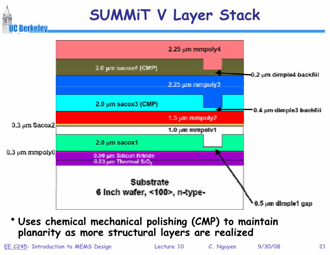
SUMMiT V Layer Stack
• Uses chemical mechanical polishing (CMP) to maintain
EE C245: Introduction to MEMS Design Lecture 10 C. Nguyen 9/30/08 21
• Uses chemical mechanical polishing (CMP) to maintain planarity as more structural layers are realized
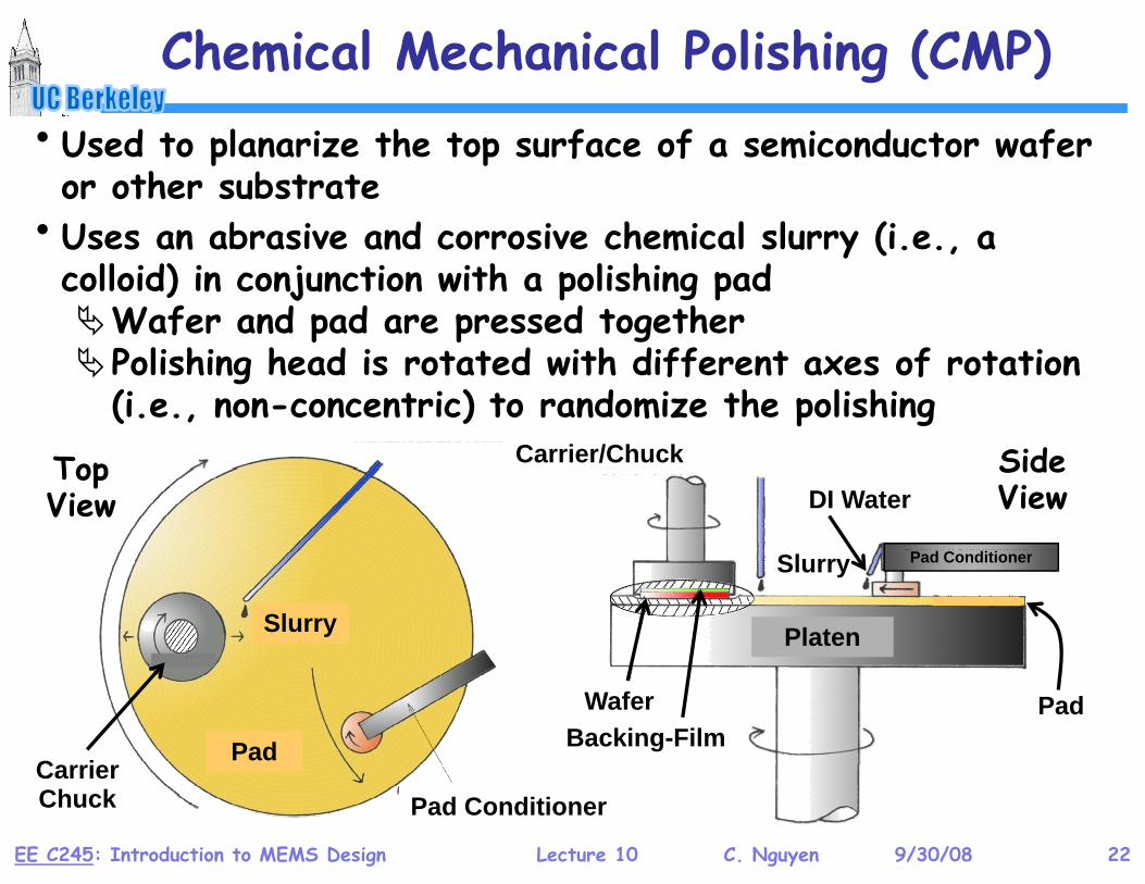
Chemical Mechanical Polishing (CMP)• Used to planarize the top surface of a semiconductor wafer or other substrate
• U b i d i h i l l (i • Uses an abrasive and corrosive chemical slurry (i.e., a colloid) in conjunction with a polishing pad
Wafer and pad are pressed togetherf p p gPolishing head is rotated with different axes of rotation (i.e., non-concentric) to randomize the polishing
Top View
Side ViewDI Water
Carrier/Chuck
Slurry Platen
Slurry Pad Conditioner
PadC i
WaferBacking-Film
Pad
EE C245: Introduction to MEMS Design Lecture 10 C. Nguyen 9/30/08 22
Pad ConditionerCarrier Chuck
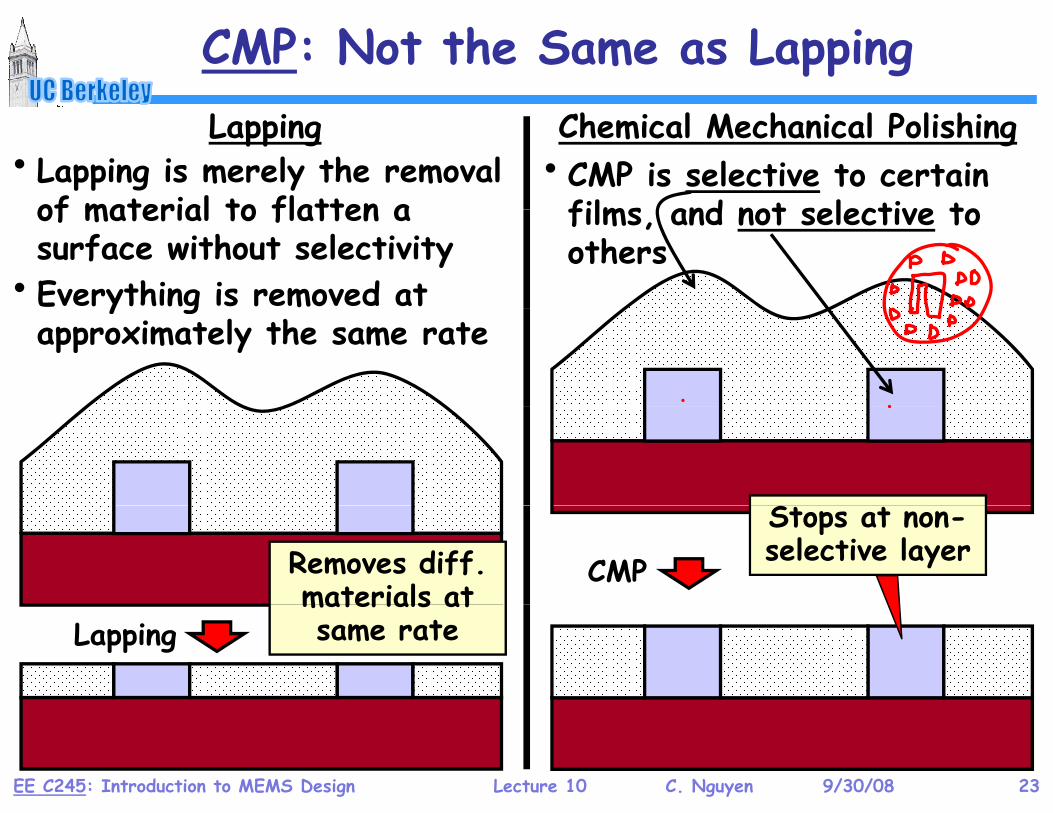
CMP: Not the Same as Lapping
• Lapping is merely the removal of material to flatten a
Lapping Chemical Mechanical Polishing• CMP is selective to certain films and not selective to of material to flatten a
surface without selectivity• Everything is removed at
films, and not selective to others
y gapproximately the same rate
CMP
Stops at non-selective layerRemoves diff.
materials at Lapping
materials at same rate
EE C245: Introduction to MEMS Design Lecture 10 C. Nguyen 9/30/08 23
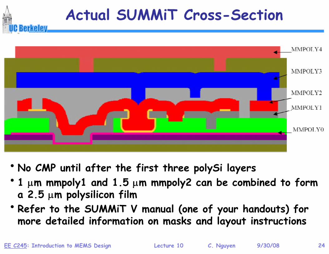
Actual SUMMiT Cross-Section
•No CMP until after the first three polySi layers• 1 μm mmpoly1 and 1.5 μm mmpoly2 can be combined to form a 2.5 μm polysilicon film
• Refer to the SUMMiT V manual (one of your handouts) for more detailed information on masks and layout instructions
EE C245: Introduction to MEMS Design Lecture 10 C. Nguyen 9/30/08 24
more detailed information on masks and layout instructions
New Topic: Mechanics of Materials
• Reading: Senturia, Chpt. 8g p• Lecture Topics:
Stress, strain, etc., for isotropic materialsThin films: thermal stress residual stress and stress Thin films: thermal stress, residual stress, and stress gradientsInternal dissipationpMEMS material properties and performance metrics
EE C245: Introduction to MEMS Design Lecture 10 C. Nguyen 9/30/08 25
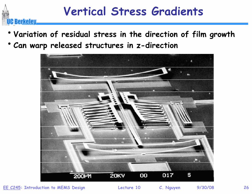
Vertical Stress Gradients
• Variation of residual stress in the direction of film growth• Can warp released structures in z-direction
EE C245: Introduction to MEMS Design Lecture 10 C. Nguyen 9/30/08 26
ElasticityElasticity
EE C245: Introduction to MEMS Design Lecture 10 C. Nguyen 9/30/08 27
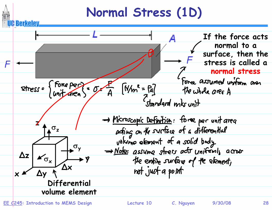
Normal Stress (1D)
If the force acts normal to a
surface then the surface, then the stress is called a
normal stressnormal stress
z σz
σy
z
∆z
x
y
Diff ti l
σx∆x
∆y
∆z
EE C245: Introduction to MEMS Design Lecture 10 C. Nguyen 9/30/08 28
Differential volume element
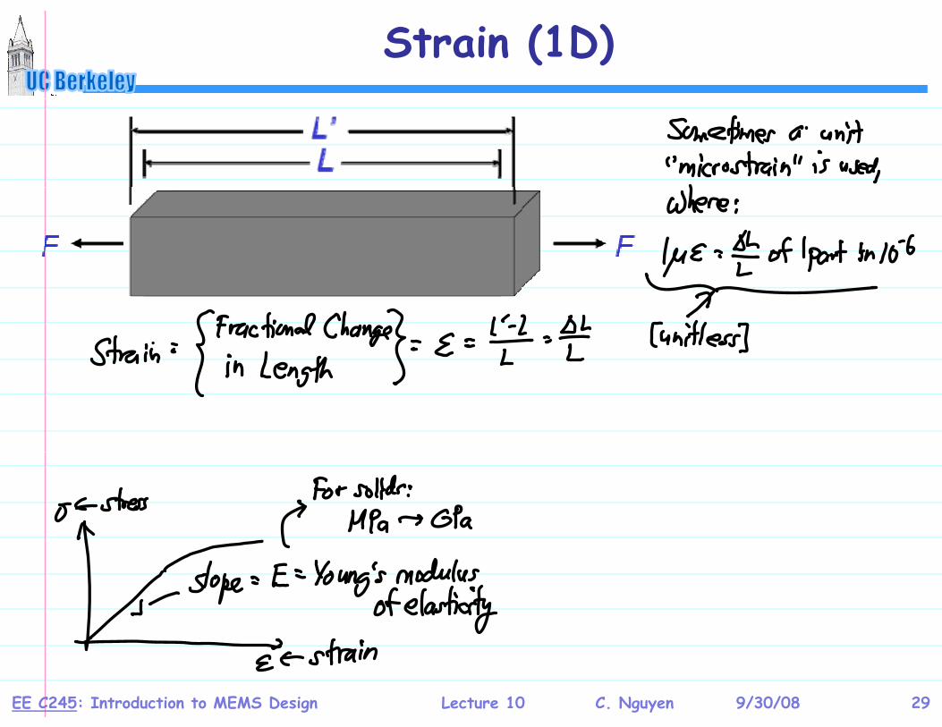
Strain (1D)
EE C245: Introduction to MEMS Design Lecture 10 C. Nguyen 9/30/08 29