Embed Size (px)
Citation preview

EE198B
Senior Project class
Fall 2001
San Jose State University
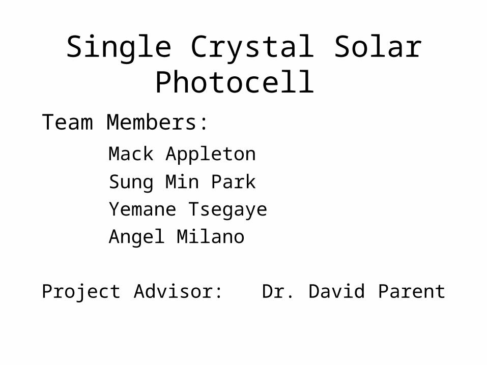
Single Crystal Solar Photocell
Team Members:
Mack Appleton
Sung Min Park
Yemane Tsegaye
Angel Milano
Project Advisor: Dr. David Parent

Project Outline
• Introduction
• Initial Testing
• Design and Simulation.
• Fabrication of Solar Cells
• Test Solar Cells
• Conclusion

Project Objective
• To design, simulate, establish and document a silicon process base-line traveler for the Single Crystal Solar Photocell.
• To enhance the relative efficiency of the Solar Photocells by 5%.

Design and Simulation
1. Maximize the efficiency
2. Anti-refraction coating.

Formula & Equations1. Rs=L/w (2D)
2. Rs = (Rn+) + (Rbar) + (Rcontact)
Rn+ = (n+ * S)/(n*b)
Rbar = (al*b)/(Wb*n)
Rcontact = c/(Wb*b)
3. = Pm/Pin = (FF*IL*Voc)/Pin
4. FF : Fill Factor (Im*Vm)/(Isc*Voc)
5. P=I*V= (I^2)*R

Design of Models
Large-grid with AR Large-grid without AR Small-grid with AR Small-grid without ARwhereLarge grid : S=3.3 cm, Wb=0.2cm, b=6.6cm, and 2
fingers.Small grid : S=0.75cm, Wb=0.2cm, b=6cm, and 8
fingers

Rs Vs Pmax
y = 0.7111e-0.1293x
0
0.2
0.4
0.6
0.8
1
1.2
0 10 20 30
Rs
Pm
ax Pmax
Expon. (Pmax)

Fabrication of Solar Cells
• Diffuse donor region• Apply aluminum coating to front of wafer• Photolithography to define solar cell
pattern• Etch aluminum to create solar cell pattern• Apply anti-reflection coating *• Apply aluminum coating to back of wafer • Anneal wafers• Remove outer edges of wafers

Diffuse Donor Region
• Spin on phosphorous doped silica glass Apply 3ml to front of wafer Spin @ 3000 rpm for 20 seconds
• Diffuse in furnace Heat furnace to 1100oc Push in wafers ½ inch per 15 seconds Diffuse for 1 hour Pull out wafers ½ inch per 15 seconds
• Makes wafer into a large diode

Apply Aluminum Coating
• Desire 2 microns thickness• Sputter on the aluminum
Accurate and precise Fast (2 microns onto 8 wafers in 15 min.) Prone to breaking down
- Or -• Evaporate on aluminum
Reliable Slow (2 microns onto 24 wafers in 3 to 4 hours) Not very precise

Photolithography
• Apply 3ml photo-resist; Spin for 20s @ 5000 rpm
• Soft bake for 90oc for 30 minutes• Place solar cell mask on wafer• Place both into wooden and glass holder• Expose under lamp for 2 minutes• Develop for 15 seconds

Etch Aluminum
• Etch exposed al using hot sulfuric acid• Rinse with DI water• Remove remaining PR using plasma etch

Apply Anti-reflection Coating
• Apply 3ml Titaniumsilicafilm• Spin @ 3000 rpm for 20 seconds
• Spreads film to thickness of 1000 angstroms
Anneal Wafers
• Anneal for 30 minutes in furnace• Creates ohmic contact between al and Si

Cleave Edges of Wafers
• Need to prevent shorting along edge of wafer• Use scribe tool to score along edges of solar
cell• Cleave wafer along scoring
Testing the Solar Cells• Scored, or roughened, back of cells• Placed onto roughened aluminum wafer• Used probes to make contacts
One probe onto the corner of the cell’s al grid One probe onto the al wafer
• Tried various methods for making good contacts Solder paste Silver paste Copper tape
Testing the Solar Cells
• Illuminated the cell Used 75W light bulb at 3cm distance
• Connected voltmeter to probe terminals Gives open circuit voltage
• Connected current source to probe terminals Ran current against that being generated by the
cells Measured voltage for different current levels

IV Curves for One Half of Grid Solar CellsPmax S13A = 41.9 mW Pmax S6A = 49.8
-250
-200
-150
-100
-50
0
50
-100 0 100 200 300 400 500 600 700
Voltage (mV)
Cu
rre
nt
(mA
)
Cell S13A (Small Grid, no AR)
Cell S6A (Small Grid, AR)

IV Curves for Small Grid Solar CellsPmax S21 = 61.4 mW Pmax S8 = 71.5 mW
-500
-400
-300
-200
-100
0
100
0 100 200 300 400 500 600 700
Voltage (mV)
Cell S8 (Small Grid, AR)
Cell S21 (Small Grid, no AR)

Conclusions
• AR cells average of 17.8% more efficient Efficiency increase = (PmaxOLD – PmaxAR)/PmaxOLD
Wanted minimum 5% increase
• Easy to follow process• Recommendations
Use the smaller grid Possible photolithography and etch of back al