Embed Size (px)
Citation preview
EE42/100 Fall 2005 Prof. Fearing 1
Week 12/ Lecture 21 Nov. 15, 2005
1. Overview of Digital Systems2. CMOS Inverter3. CMOS Gates4. Digital Logic5. Combinational Blocks 6. Latches and Flip Flops7. Registers and Counters
Reading: Hambley 12.7, 7
EE42/100 Fall 2005 Prof. Fearing 2
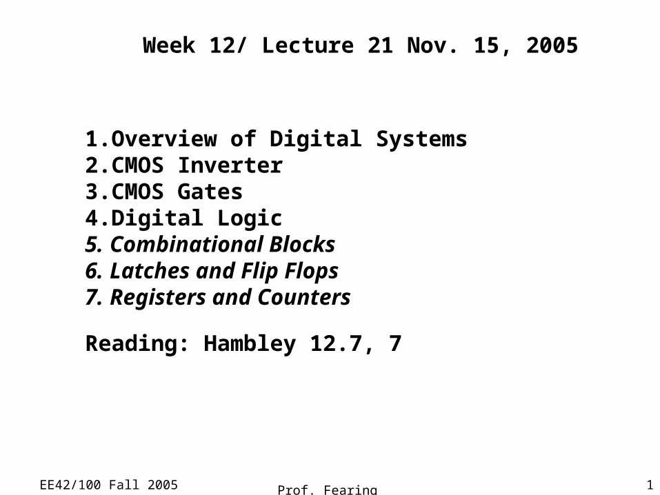
1. Digital System Overview
I/O module
EE42/100 Fall 2005 Prof. Fearing 3
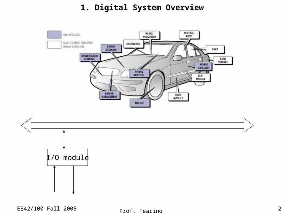
1.1 IO Module
CPU
A/D
Sensors Actuators
amplifier/filter amplifier/switch
D/A
serial/parallel conversion
communications
EE42/100 Fall 2005 Prof. Fearing 4
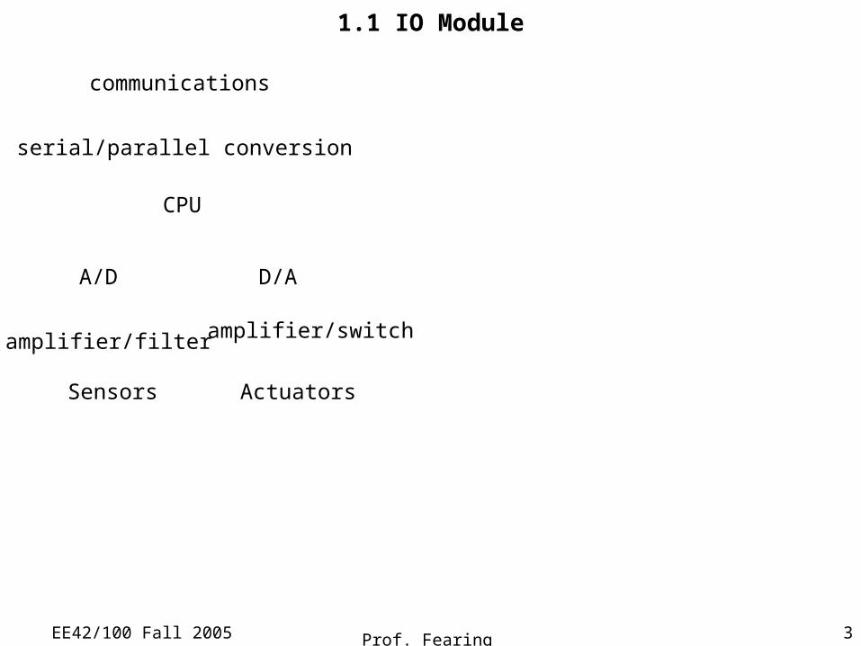
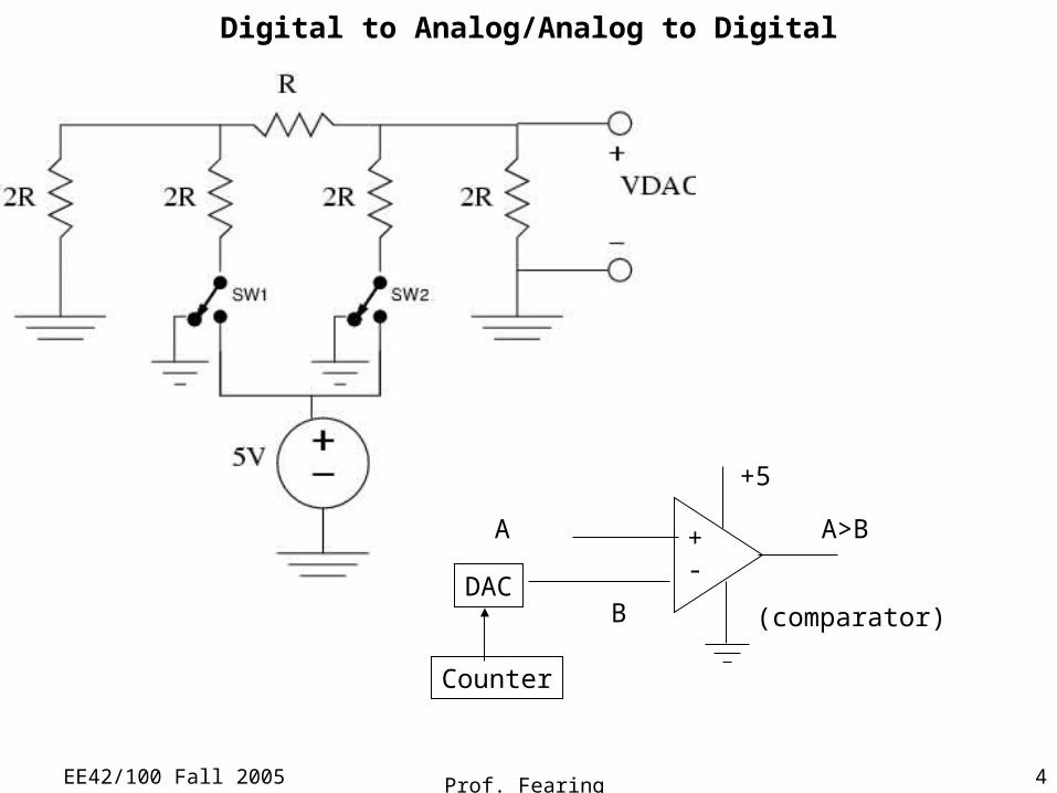
Digital to Analog/Analog to Digital
+-
+5
A>BA
DACB
Counter
(comparator)
EE42/100 Fall 2005 Prof. Fearing 5
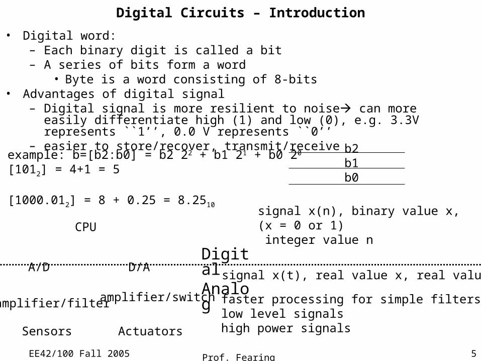
Digital Circuits – Introduction
• Digital word:– Each binary digit is called a bit– A series of bits form a word
• Byte is a word consisting of 8-bits• Advantages of digital signal
– Digital signal is more resilient to noise can more easily differentiate high (1) and low (0), e.g. 3.3V represents ``1’’, 0.0 V represents ``0’’
– easier to store/recover, transmit/receive
CPU
A/D
Sensors Actuators
amplifier/switch
D/A
amplifier/filter
DigitalAnalog signal x(t), real value x, real value t
signal x(n), binary value x, (x = 0 or 1) integer value n
faster processing for simple filterslow level signalshigh power signals
example: b=[b2:b0] = b2 22 + b1 21 + b0 20
[1012] = 4+1 = 5
[1000.012] = 8 + 0.25 = 8.2510
b2b1b0
EE42/100 Fall 2005 Prof. Fearing 6
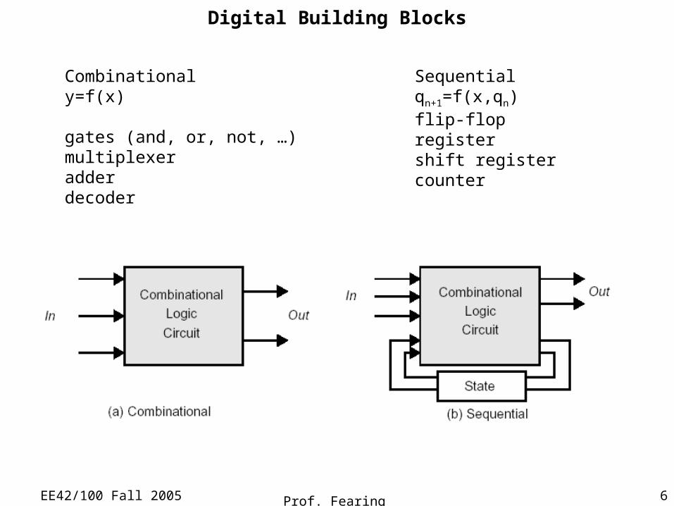
Digital Building Blocks
Combinationaly=f(x)
gates (and, or, not, …)multiplexeradderdecoder
Sequentialqn+1=f(x,qn)flip-flopregistershift registercounter
EE42/100 Fall 2005 Prof. Fearing 7
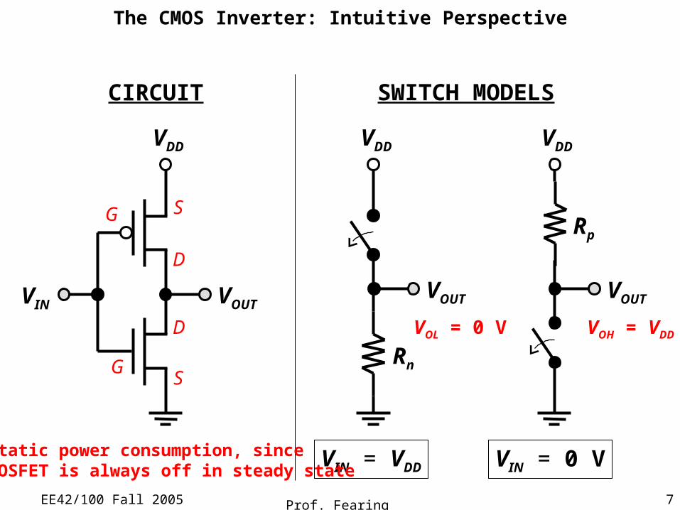
The CMOS Inverter: Intuitive Perspective
VDD
Rn
VIN = VDD
CIRCUIT SWITCH MODELS
VDD
Rp
VIN = 0 V
VOUT VOUT
VOL = 0 V VOH = VDD
Low static power consumption, sinceone MOSFET is always off in steady state
VDD
VIN VOUT
S
D
G
GS
D
EE42/100 Fall 2005 Prof. Fearing 8
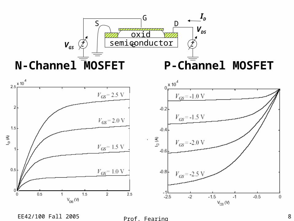
N-Channel MOSFET P-Channel MOSFET
VGS
S
semiconductoroxide
G
VDS
ID
+ +
D
EE42/100 Fall 2005 Prof. Fearing 9
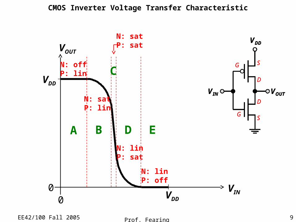
CMOS Inverter Voltage Transfer Characteristic
VIN
VOUT
VDD
VDD00
N: offP: lin
N: linP: off
N: linP: sat
N: satP: lin
N: satP: sat
VDD
VIN VOUT
S
D
G
GS
D
VDD
VIN VOUT
VDD
VIN VOUT
S
D
G
GS
D
A B D E
C
EE42/100 Fall 2005 Prof. Fearing 10
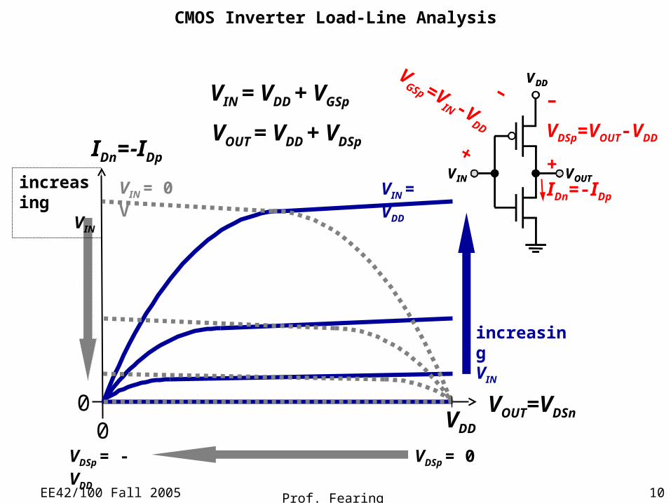
CMOS Inverter Load-Line Analysis
VOUT=VDSn
IDn=-IDp
0
VDD
VIN VOUT
VDD
VIN VOUT
IDn=-IDp
–V
GSp =VIN -V
DD
+
VIN = VDD + VGSp
increasingVIN
increasingVIN
VIN = 0 V VIN = VDD
VDD
VOUT = VDD + VDSp
VDSp = 0VDSp = - VDD
–
VDSp=VOUT-VDD
+
0
EE42/100 Fall 2005 Prof. Fearing 11
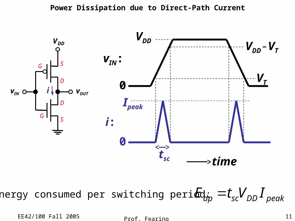
Power Dissipation due to Direct-Path Current
VDD-VT
VT
time
vIN:
i:
Ipeak
VDD
0
0
i
S
D
G
GS
D
VDD
vOUTvIN
peakDDscdp IVtE =Energy consumed per switching period:
tsc
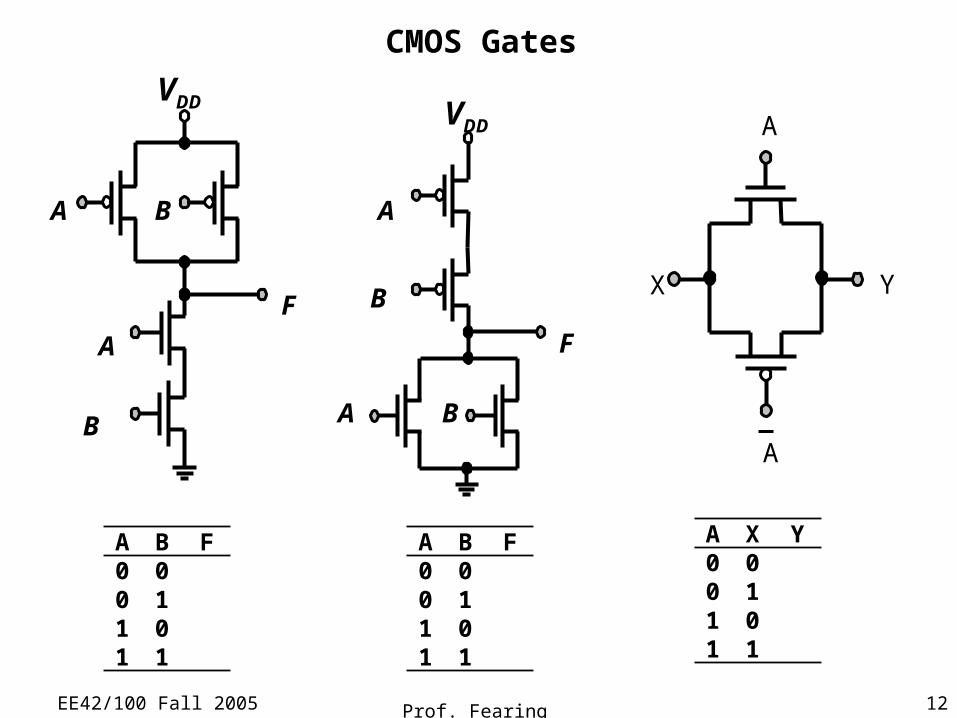
EE42/100 Fall 2005 Prof. Fearing 12
A B F0 00 11 01 1
A
F
B
A B
VDD
BA
F
A
B
VDD
A B F0 00 11 01 1
CMOS Gates
A
X Y
A
A X Y0 00 11 01 1
EE42/100 Fall 2005 Prof. Fearing 13
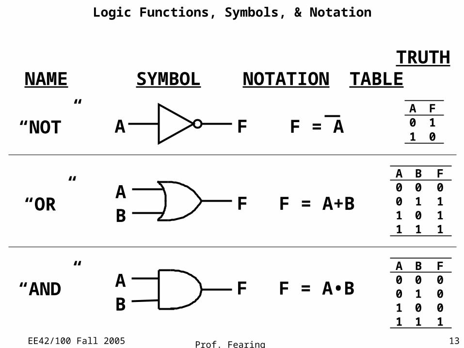
Logic Functions, Symbols, & Notation
“NOT” F = A
TRUTHNAME SYMBOL NOTATION TABLE
FA
A B F0 0 00 1 01 0 01 1 1
“OR” F = A+BFAB
A F0 11 0
A B F0 0 00 1 11 0 11 1 1
“AND” F = A•BFAB
EE42/100 Fall 2005 Prof. Fearing 14
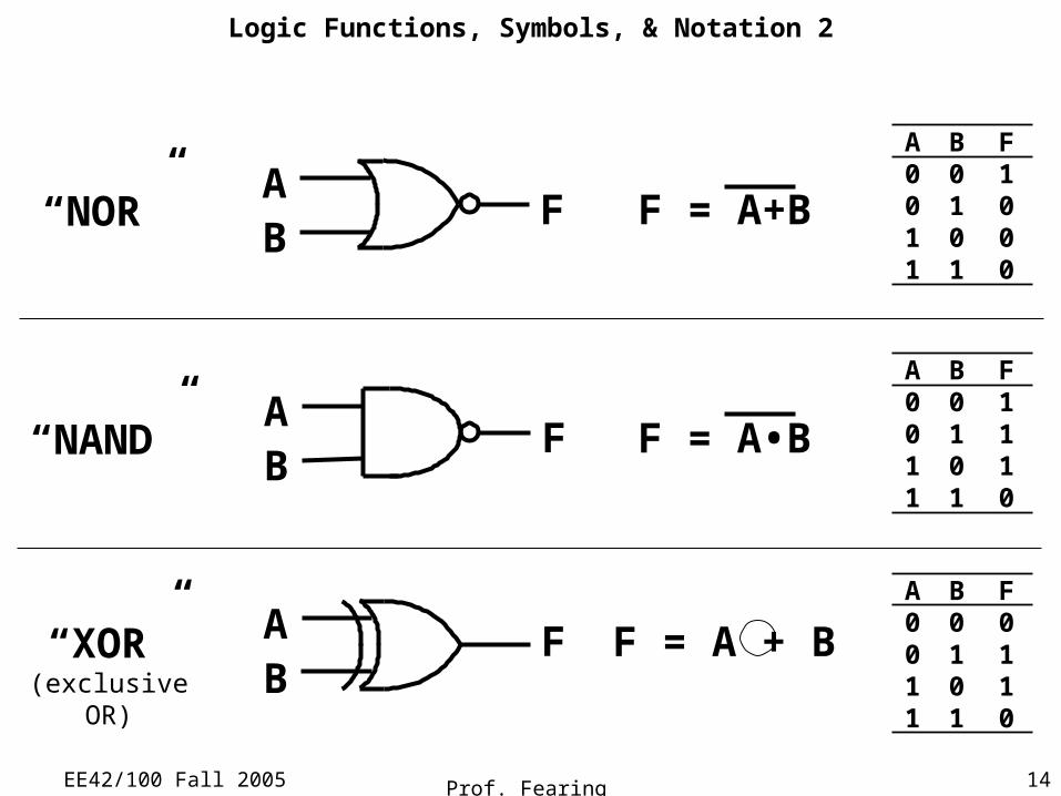
Logic Functions, Symbols, & Notation 2
“NOR” F = A+B
A B F0 0 00 1 11 0 11 1 0
“NAND” F = A•BFAB
A B F0 0 10 1 11 0 11 1 0
“XOR”(exclusive OR)
F = A + BFAB
FAB
A B F0 0 10 1 01 0 01 1 0
EE42/100 Fall 2005 Prof. Fearing 15
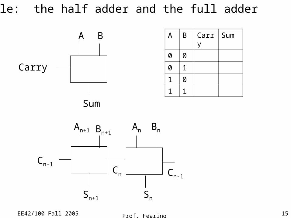
Example: the half adder and the full adder
A B
Carry
Sum
An+1 Bn+1
Cn+1
Sn+1
Cn
Sn
An Bn
Cn-1
A B Carry Sum
0 0
0 1
1 0
1 1
EE42/100 Fall 2005 Prof. Fearing 16
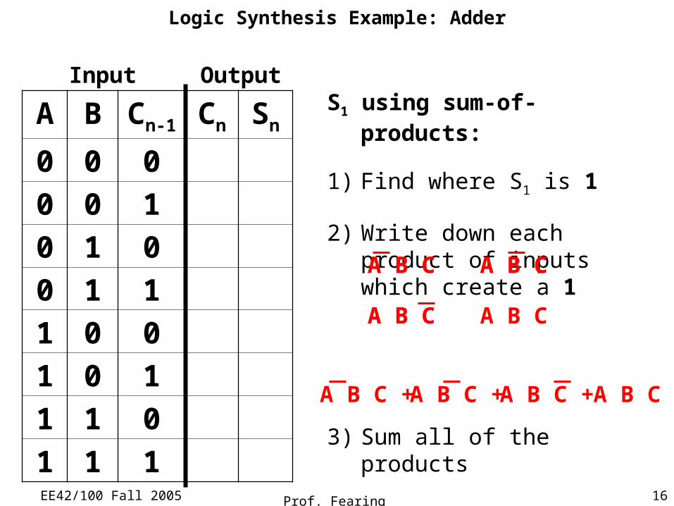
S1 using sum-of-products:
1) Find where S1 is 1
2) Write down each product of inputs which create a 1
3) Sum all of the products
4) Draw the logic circuit
Logic Synthesis Example: Adder
A B Cn-1 Cn Sn
0 0 0
0 0 1
0 1 0
0 1 1
1 0 0
1 0 1
1 1 0
1 1 1
Input Output
A B C A B C
A B C A B C
A B C + A B C + A B C + A B C
A B C A B C
A B C
EE42/100 Fall 2005 Prof. Fearing 17
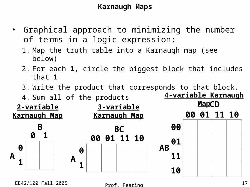
Karnaugh Maps
• Graphical approach to minimizing the number of terms in a logic expression:1. Map the truth table into a Karnaugh map (see below)
2. For each 1, circle the biggest block that includes that 1
3. Write the product that corresponds to that block.
4. Sum all of the products
A
B
2-variableKarnaugh Map
0 1
1
0A
1
0
BC00 01 11 10
3-variableKarnaugh Map
4-variable Karnaugh Map
CD00 01 11 10
AB
00
01
11
10
EE42/100 Fall 2005 Prof. Fearing 18
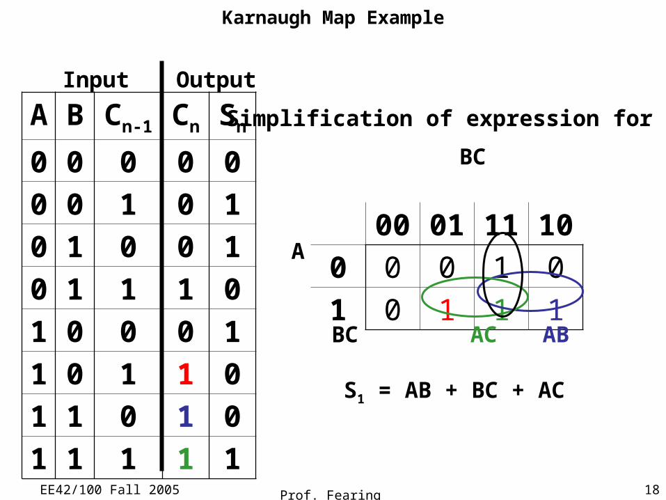
A B Cn-1 Cn Sn
0 0 0 0 0
0 0 1 0 1
0 1 0 0 1
0 1 1 1 0
1 0 0 0 1
1 0 1 1 0
1 1 0 1 0
1 1 1 1 1
Input Output
00 01 11 10
0 0 0 1 0
1 0 1 1 1
A
BC
BC AC AB
S1 = AB + BC + AC
Simplification of expression for S1:
Karnaugh Map Example