Embed Size (px)
Citation preview
EE457 Final - Fall 2020 1 / 17 C Copyright 2020 Gandhi Puvvada
EE457 Final Exam (~34%)(31% or 37%)Open-book Open-notes Exam just for the Fall 2020;
No calculators. Verilog Guides are not needed and are not allowed.Smart phones, tablets, and all kinds of computing/Internet devices are allowed for writing your exam and for communicating with your proctor.
You should not be communicating with anyone other than your proctor during the entire period of the exam.This is a Crowdmark exam. Please do not write on margins or on the backside.
Fall 2020Instructor: Gandhi Puvvada
Saturday 11/21/2020 (A 3-hour exam) nominally 01:30 PM - 04:30 PM (180 min) on Zoom
Viterbi School of EngineeringUniversity of Southern California
Ques# Topic Page# Time Points Score
1 Lab 7 modified 2-122 Cache and Virtual Memory 13-143 Tomasulo OoO 15-164 CMP, MOESI, CMT, 17
Total 17 = Cover+16
Perfect Score
I have previously read the Viterbi Code of Integrity and other related material at the site https://viterbischool.usc.edu/academic-integrity/ and I will abide by these rules of conduct. I will neither seek help from others nor offer help to others in my exams.
_____________________________ <== Student’s signature
Cover page

EE457 Final - Fall 2020 2 / 17 C Copyright 2020 Gandhi Puvvada
1 ( points) min. Lab 7 modified
This design is derived from your midterm question on Lab 7. An incomplete block diagram for this question is provided on page 4. The solution for your midterm question and the solution for the Spring 2019 Final question are provided on pages 5 and 6 for your reference.
Besides the A2, A3, M, and MA of the Midterm exam question, here we added a BXZ (Branch if X is a zero) instruction like in the Spring 2019 Final Q#1. Here also an early branch from ID stage is planned.
Instruction Operation One-Hot Coded
NOP 0 0 0 0 0
A2 $R, $X, $Y; ($R) <= ($X)+($Y) 1 0 0 0 0
A3 $R, $X, $Y, $Z; ($R) <= ($X)+($Y)+($Z) 0 1 0 0 0
M $R, $X, $Y; ($R) <= ($X)*($Y) 0 0 1 0 0
MA $R, $X, $Y, $Z; ($R) <= ($X)*($Y)+($Z) 0 0 0 1 0
BXZ $X, JJJJ; (PC) <= JJJJ if ($X == 0) 0 0 0 0 1 Note: Here PC is 16 bits in size. JJJJ is 16 bits.
Significant aspects of the current design:
1. A dummy stage, D, between the EX1 and EX2 stages, like in the Fall 2019 Final Q#1.
2. Instruction Cache (in the IF stage) produces ICM (Instruction Cache Miss). ICM causes stalling IF stage and injecting bubbles into later stages.
3. Instead of having all comparison units in a comparison station in the ID stage, here, we went back to the Lab 6 Part 4 method, where needed register ID comparisons are done in the individual stages (though it amounts to replication of comparison units). There is a HDU in the ID stage and a FU in each of the four stages: ID, EX1, D, and EX2. So, you can write (EX2_ZA = WB_RA) in the pseudo code/gate-level design of the FU in the EX2 instead of the lab 7 designation of EX2_ZMEX1. To facilitate the Lab 6 method, we carried the source register IDs (XA, YA, and ZA) through the stage registers so as to tap them as needed for comparison with the destination register IDs (RAs) of their seniors.
4. The provided incomplete design is excessive when it comes to forwarding muxes. Muxes are provided, whether they are needed or not, to receive help from all/several seniors. Please cross off of unneeded muxes first. Then review and cross off unneeded conveyances of XA, YA, ZA through the pipe. For example, they are not needed in the WB stage. Do you need all the three or a subset of them in the EX2 stage?
5. ETM_EX1 (Extra Time for Mult in EX1): We provided only one extra clock for the Mult operation in the Midterm design. Here Mult needs two extra clocks (total three clocks). So, you need to activate STALL_M for the first two clocks and inactivate it in the third clock.
6. STALL_M was stalling the entire pipe in the Midterm design. Here, we do better. Here, STALL_M does not stall junior instructions in ID and IF stages if the ID stage is occupied by a BXZ instruction. Of course, the BXZ can stall on its own. Otherwise the BXZ can execute while STALL_M is active and vanish! There is no need for the BXZ to walk through the rest of the pipeline (EX1, D, EX2 stages).
Q1P2

EE457 Final - Fall 2020 3 / 17 C Copyright 2020 Gandhi Puvvada
7. Bubble Injection: You agree with student ____________ (#1 / #2 / #3 / #4)Student #1: I inject a bubble into the next stage, if the next stage is being stalled.Student #2: I inject a bubble into the next stage, if both my stage and the next stage are being stalled.Student #3: If I stall a stage, I inject a bubble into the next stage, if the next stage is not being stalled.Student #4: I agree with student #3’s plan but I will simplify the same. If I stall a stage, I activate bubble injection into the next stage and I do not care if the next stage is being stalled or not. If the next stage is being stalled, well the bubble, that I tried to inject, does not go anywhere and that is fine!
7.A. One student points out that in the Spring 2019 Final Q#1, the bubble-inject-ing AND gates in the ID stage were crossed off as shown on the side. Hence he wants to cross them off in the current design also. You _________ (agree/disagree) with him. Explain:__________________________________________________________________________________________________________________________________________________________________________________________________________________________________________________________________________________________________________________________________________
Blank Area for any rough work
Q1P3

EE457 Final - Fall 2020 4 / 17C
Copyright 2020 G
andhi Puvvada
PC
ZA
YA
XA
ZD
YD
XD
Reg. File
ZA
YA
XA
RA
RD
R-Write
EN_IDEX1
0
1
0
1
0
1
0
1
A
B Add
er/M
ultip
lier
S
A
B
S
Add
er
IF ID EX1 EX2
Y3Mux
X3Mux
Z6MuxZ7Mux
ZDEN
INS-
ME
MWB
ID_XA
ID_YA
ID_ZA
EN_IFID
Writ
e
XY
D
XD
+YD
+ZD
XD
YD
ZD
STALL_D STALL_DB
FX3M
FY3M
FZ6MFZ7M
WB
_RD
WB
_WR
ITE
0
1
R1Mux
SKIP
A / M
MA
M
A3
A2
MA
M
A3
A2
MA
M
A3
A2
0
1
0
1
Y2Mux
X2Mux
FX2M
FY2M
EX2_Write
RR R R
R
STALL_M STALL_MB
EX1_Write
BXZ
ICM
ID_B
XZ
0
1
0
1
0
1
Z0Mux
Y0Mux
X0Mux
FZ0M
FY0M
FX0M
0
1
Z4Mux
ZD
EN_EX1D
XY
D
FZ4M
MA
M
A3
A2
R
0
1
XY6Mux
FXY6M
0
1
XY5Mux
FXY5M
0
1
0
1
Y4Mux
X4Mux
FX4M
FY4M0
1
XY7Mux
FXY7M
WB
_RA
WB
_RD
WB_WRITE
0
1
Z3Mux
FZ3M
0
1
Z2Mux
FZ2M
0
1
Z5Mux
FZ5M
D_Write
0
1
0
1
0
1
Z1Mux
Y1Mux
X1Mux
FZ1M
FY1M
FX1M
D
XZ
+1
16
0
1
16
BR1
16
(X=ZERO)
JJJJ
XA
YA
ZARA
XA
YA
ZARA
XA
YA
ZARA
XA
YA
ZARA
XA
YA
ZARA
D_XAD_YAD_ZA
D_RA
EX1_XAEX1_YAEX1_ZA
EX1_RA
ID_XAID_YAID_ZA
ID_RA
EX2_XAEX2_YAEX2_ZA
EX2_RA
WB_XA
WB_YAWB_ZA
WB_RA
HDU_ID FU_ID FU_EX1 FU_D FU_EX2
STALL_D
ETM_EX1STALL_M
Extra Time for Mult (ETM)
EX2_Write
ENENEN
EN_DEX2
Lab 7 modified with a dummy stage
1. Cross off unneeded/redundant/unwanted forwarding muxes.2. Complete forwarding paths to the remaining (surviving) forwarding muxes. 6. Complete two enable (EN) controls on PC and the IF/ID.
5. Generate STALL_D and STALL_M (Stall for Multiply).
7. Complete all Bubble Injection (BI) controls.8. For the four FUs (forwarding units), draw the input (only input, no output) pins and generate one per category. For example, if multiple FX-- and FY-- are to
On this pageOn the next few pages
3. Cross off unneeded/unwanted portions of source-address (XA, YA, ZA)
BI_IF
BI_ID
conveyance lines and the associated FFs.
be produced by the FU, just generate one FX-- and one FY-- of your choice.
EN_PC
EN_EX2WB
4. Complete the 4 enables for the ID/EX1, EX1/D, D/EX2, EX2/WB
Current exam
question for completion
Q1P4
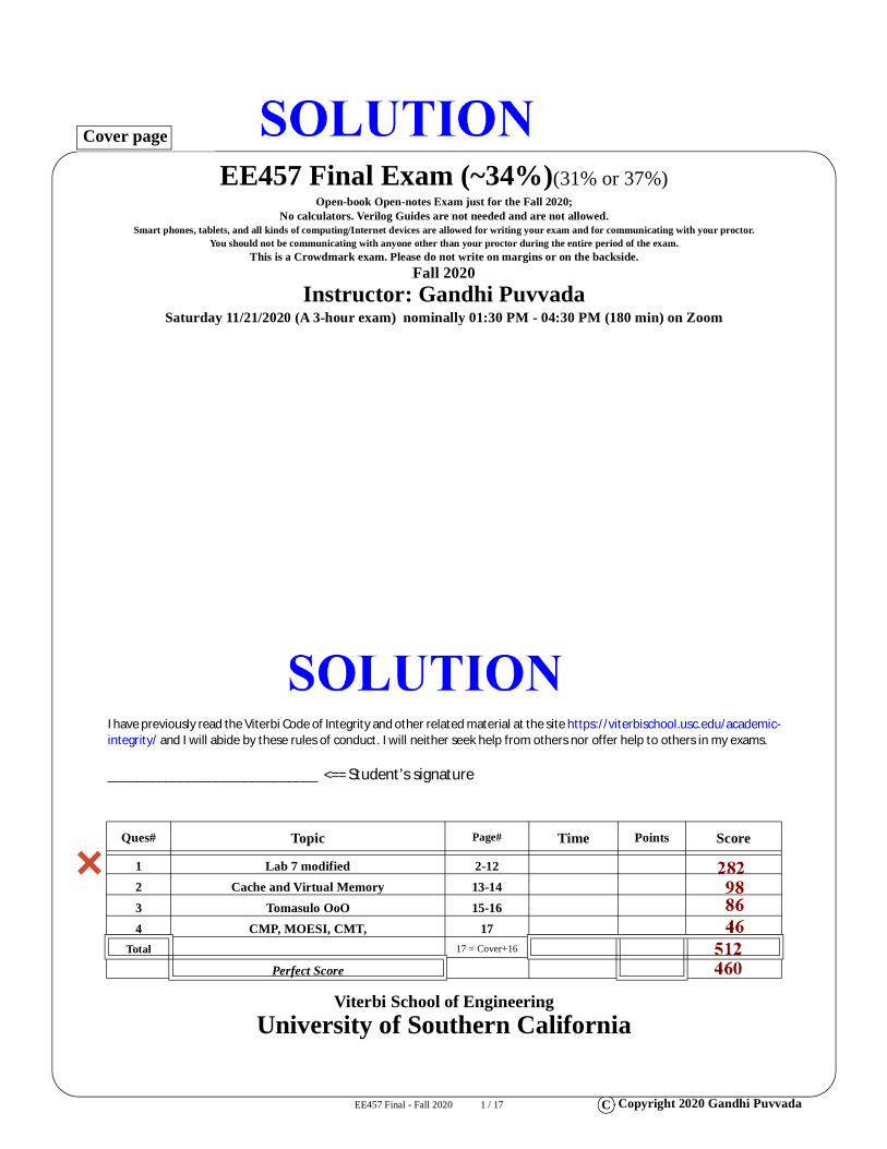
EE457 Final - Fall 2020 5 / 17C
Copyright 2020 G
andhi Puvvada
EE457 Fall 2020 Midterm
pipeline Q solution For R
eference onlyN
on-grading page, Don’t subm
it
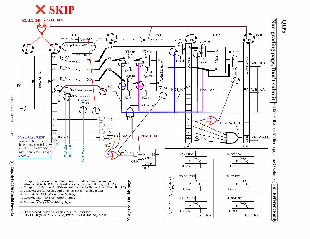
Q1P5
EE457 Final - Fall 2020 6 / 17C
Copyright 2020 G
andhi Puvvada
EE457 Spring 2019 Final pipeline Q solution For R
eference onlyN
on-grading page, Don’t subm
itQ
1P6

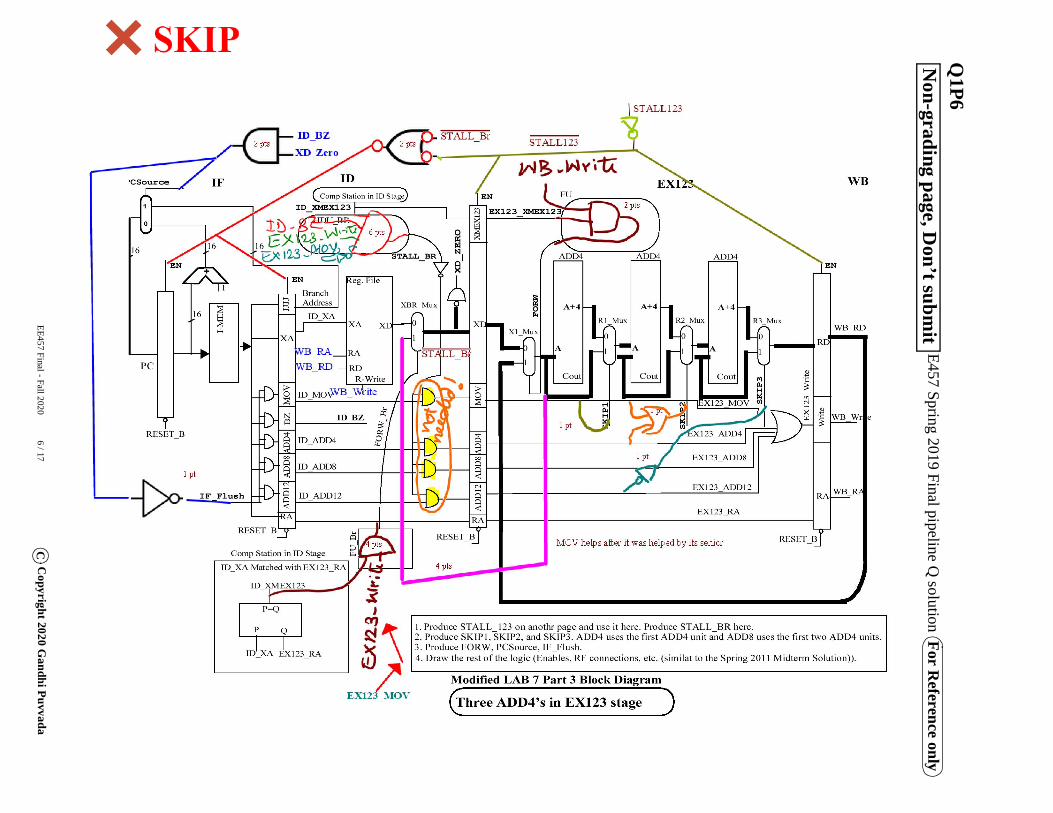
EE457 Final - Fall 2020 7 / 17C
Copyright 2020 G
andhi Puvvada
ee457_early_branch_block_diagram For R
eference onlyN
on-grading page, Don’t subm
itQ
1P7

EE457 Final - Fall 2020 8 / 17 C Copyright 2020 Gandhi Puvvada
Generate STALL_D. Draw gates. Do not bother to do logic minimization.
Let us do thesetasks.
6. Complete two enable (EN) controls on PC and the IF/ID.5. Generate STALL_D and STALL_M (Stall for Multiply).
7. Complete all Bubble Injection (BI) controls.8. For the four FUs (forwarding units), draw the input (only input, no output) pins and generate one per category. For example, if multiple FX-- and FY-- are to
On the next few pages
be produced by the FU, just generate one FX-- and one FY-- of your choice.
STALL_D
Dependency
in the ID stage
ID_BXZBranch related stall
Non-Branch related stall
PS1: ProblematicSenior #1
PS2
PS3
DS1: DifficultSenior #1
DS2
STALL
BRS_D
NBRS_D
Q1P8

EE457 Final - Fall 2020 9 / 17 C Copyright 2020 Gandhi Puvvada
Generate STALL_M. Multiply (M or MA) needs 3 clocks (i.e. two extra clocks)
Assume one-hot implementation for each of the above two state diagrams
C1
C1
1
FC SC TC
If C1, activate STALL_M
KeepSTALL_Mactive.
Release
RESET_B
C3
C3
C4
FiC SubC
If C3, activate STALL_M
If ________, continueSTALL_Melse release it.
RESET_B
I <= 0;I <= I + 1;
C4
STALL_M
SD#1 (State Diagram #1)
SD#2 (State Diagram #2) complete itIf it doesn’t fit there, write it outside
STALL_M STALL_MB
ETM_EX1STALL_M
Extra Time for Mult (ETM)
C1
SD#1 (State Diagram #1)
STALL_M
C3
SD#2 (State Diagram #2)
C4
STALL_M
2 pts
2 pts
2 pts
6 pts 6 pts
Blank Area for any rough work
Q1P9
EE457 Final - Fall 2020 10 / 17 C Copyright 2020 Gandhi Puvvada
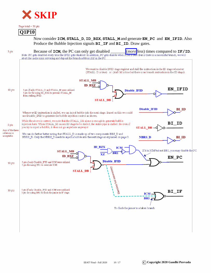
Now consider ICM, STALL_D, ID_BZX, STALL_M and generate EN_PC and EN_IFID. Also Produce the Bubble Injection signals BI_IF and BI_ID. Draw gates.
Because of ICM, the PC can only get disabled _______ (more/less) times compared to IF/ID.
BI_ID
EN_IFID
BI_IF
EN_PC
Blank Area for any rough work
Q1P10

EE457 Final - Fall 2020 11 / 17 C Copyright 2020 Gandhi Puvvada
Now design the FUs (Forwarding Units) partially. Draw input pins of each FU completely. We assume that the output pins are basically same as all the surviving mux select control lines for that stage. Please produce (by drawing gates) only one forwarding control signal per category. For example, if multiple FX-- and FY-- are to be produced by the FU, just generate one FX-- and one FY-- of your choice. Recall that _________(FU/STALL) logic can be a little simplistic because of its guardian angel namely the _________(FU/STALL) logic. You _____ (A/B). A = need to consider priority in forwarding, B = do not need to consider priority because relative priority is taken care off by natural ordering of the forwarding muxes. For each FU, write down the number of 4-bit comparison units needed to compare register IDs in the little squares. Note that $0 is like any other register. Take a quick look at your Lab 6 early branch block diagram provided on page 7. The provided partial input pins may or may not be complete.
FU_ID
ID_XA _RA_Write_RA_Write
FU_EX2
ID_XA _RA_Write_RA_Write
Q1P11

EE457 Final - Fall 2020 12 / 17 C Copyright 2020 Gandhi Puvvada
FU_D
_RA_Write
FU_D
_RA_Write
Blank Area for any rough work
Q1P12

EE457 Final - Fall 2020 13 / 17 C Copyright 2020 Gandhi Puvvada
2 ( points) min. Cache and Virtual Memory
2.1 LW $2, 4000($4) instruction was executed on CPU with 2-level TLB, 4-level page table, and 3-level data cache. It had a cache hit in L3 cache, but it took much longer compared to another such instruction which also had a cache hit in L3 cache. What could be the difference? Narrate the sequence of events in the shortest cache hit in L3 cache and the longest cache hit in L3 cache.____________________________________________________________________________ ____________________________________________________________________________ ____________________________________________________________________________ ____________________________________________________________________________ ____________________________________________________________________________ ____________________________________________________________________________ Is it true that in both cases, since it is a cache hit, you do not have to go to the MM (Main Memory at all? _______ (T/F) in the shortest case above and _______ (T/F) in the longest case above.
2.2 Consider the case of a CPU with a 1-level TLB and a 1-level cache. Since every memory access has to go through the TLB and the cache at minimum and occasionally to the PT (Page Table) in case of a TLB miss and to the MM Data Page in case of a cache miss, can we say that the TLB miss rate is much higher than the cache miss rate, if the TLB is a 64-entry TLB, which is much smaller than the 64KB Cache? ________ (Yes/No). Explain ____________________________ ____________________________________________________________________________ ____________________________________________________________________________ ____________________________________________________________________________ ____________________________________________________________________________ ____________________________________________________________________________ ____________________________________________________________________________
2.3 If you want to decrease page size from 4KB to 1KB, then you need to consider _____________ (increasing/decreasing) the TLB size. It also causes an _________________ (increase/decrease) of the Page Table size. If you do decrease the page size to 1KB, a change is TLB size is _______ (A/B) and a change in PT size is ______ (A/B), where A = a design decision, B = a consequent effect.
2.4 It is more common to have higher a DoSA (Degree of Set Associativity) in a ________ (TLB/Cache) mapping. In ________ (a TLB/a Cache/both/neither), the number of TAG RAMs is equal to the DoSA.
2.5 For the same 64KB cache, a DoSA of 8, as compared to a DoSA of 2, is ________ (more/less expensive. The TAG RAMs are _____________ (more/fewer/same) in number, _____________ (taller/shorter/same) in height, and _____________ (wider/narrower/same) in width. The DATA RAMs are _____________ (more/fewer/same) in number, _____________ (taller/shorter/same) in height, and _____________ (wider/narrower/same) in width.
Q2P13
EE457 Final - Fall 2020 14 / 17 C Copyright 2020 Gandhi Puvvada
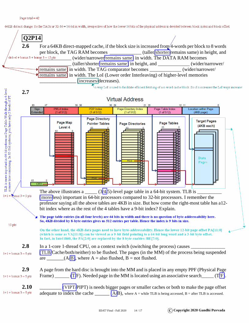
2.6 For a 64KB direct-mapped cache, if the block size is increased from 4-words per block to 8 words per block, the TAG RAM becomes _____________ (taller/shorter/remains same) in height, and _____________ (wider/narrower/remains same) in width. The DATA RAM becomes _____________ (taller/shorter/remains same) in height, and _____________ (wider/narrower/remains same) in width. The TAG comparator becomes _____________ (wider/narrower/remains same) in width. The LoI (Lower order Interleaving) of higher-level memories _______________ (increases/decreases).
2.7
The above illustrates a _____ (3/4/5)-level page table in a 64-bit system. TLB is __________ (more/less) important in 64-bit processors compared to 32-bit processors. I remember the professor saying all the above tables are 4KB in size. But how come the right-most table has a12-bit index where as the rest of the 4 tables have a 9-bit index? Explain.____________________________________________________________________________ ____________________________________________________________________________ ____________________________________________________________________________ ____________________________________________________________________________
2.8 In a 1-core 1-thread CPU, on a context switch (switching the process) causes ______________ (TLB/Cache/both/neither) to be flushed. The pages (in the MM) of the process being suspended are _______(A/B), where A = also flushed, B = not flushed.
2.9 A page from the hard disc is brought into the MM and is placed in any empty PPF (Physical Page Frame) ______ (T/F). Needed page in the MM is located using an associative search_____ (T/F).
2.10 _________ (VIPT/PIPT) is needs bigger pages or smaller caches or both to make the page offset adequate to index the cache ______ (A/B), where A = while TLB is being accessed, B = after TLB is accessed.
Q2P14
EE457 Final - Fall 2020 15 / 17 C Copyright 2020 Gandhi Puvvada
3 ( points) min. Tomasulo OoC and IoC
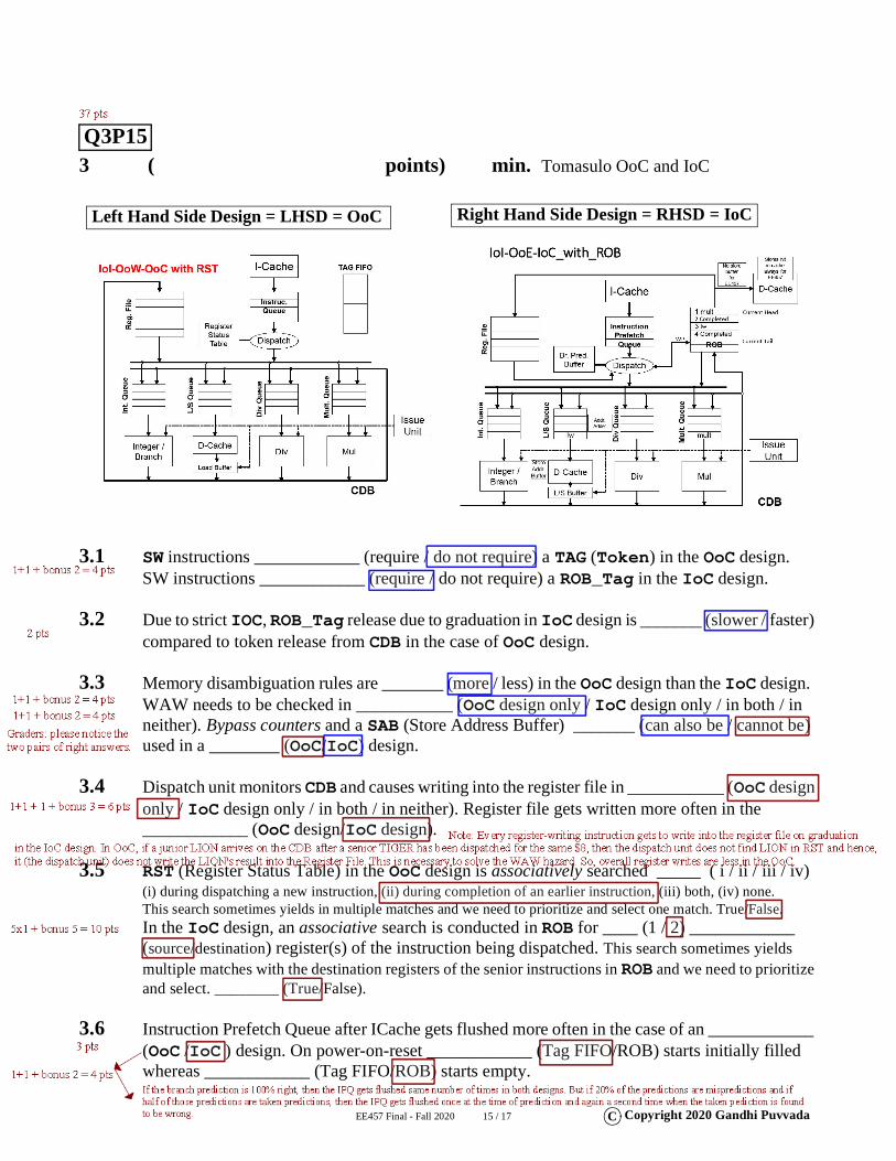
3.1 SW instructions ____________ (require / do not require) a TAG (Token) in the OoC design.SW instructions ____________ (require / do not require) a ROB_Tag in the IoC design.
3.2 Due to strict IOC, ROB_Tag release due to graduation in IoC design is _______ (slower / faster) compared to token release from CDB in the case of OoC design.
3.3 Memory disambiguation rules are _______ (more / less) in the OoC design than the IoC design. WAW needs to be checked in ___________ (OoC design only / IoC design only / in both / in neither). Bypass counters and a SAB (Store Address Buffer) _______ (can also be / cannot be) used in a ________ (OoC/IoC) design.
3.4 Dispatch unit monitors CDB and causes writing into the register file in ___________ (OoC design only / IoC design only / in both / in neither). Register file gets written more often in the ____________ (OoC design/IoC design).
3.5 RST (Register Status Table) in the OoC design is associatively searched _____ ( i / ii / iii / iv)(i) during dispatching a new instruction, (ii) during completion of an earlier instruction, (iii) both, (iv) none.This search sometimes yields in multiple matches and we need to prioritize and select one match. True/False.In the IoC design, an associative search is conducted in ROB for ____ (1 / 2) ____________ (source/destination) register(s) of the instruction being dispatched. This search sometimes yields multiple matches with the destination registers of the senior instructions in ROB and we need to prioritize and select. ________ (True/False).
3.6 Instruction Prefetch Queue after ICache gets flushed more often in the case of an ____________ (OoC /IoC ) design. On power-on-reset ____________ (Tag FIFO/ROB) starts initially filled whereas ____________ (Tag FIFO/ROB) starts empty.
Left Hand Side Design = LHSD = OoC Right Hand Side Design = RHSD = IoC
Q3P15
EE457 Final - Fall 2020 16 / 17 C Copyright 2020 Gandhi Puvvada
3.7 CDB: The capacitance associated with the CDB is so ________ (high/little) that it _________ (needs/does not need) a clock for itself. The CDB register shown on the right is needed in _______________ (the OoC / the IoC / both / neither) design(s).
3.8 RAS (Return Address Stack) is not shown in both the block diagrams, but is appropriate in the ______ (OoC/IoC) design where as it is inappropriate in the ______ (OoC/IoC) design. Explain.____________________________________________________________________________ ____________________________________________________________________________ ____________________________________________________________________________
3.9 System Stack follows _______ (LIFO/FIFO) order and ________ (is/isn’t) circular. RAS follows _______ (LIFO/FIFO) order and ________ (is/isn’t) circular.Since stack pointer points to the top of the stack, to PUSH an item on to the stack, one has to advance the stack pointer and place an item on the stack. It takes _______ (1 clock only/2 clocks) to PUSH an item on RAS. Explain. _______________________________________________ ____________________________________________________________________________ ____________________________________________________________________________ ____________________________________________________________________________
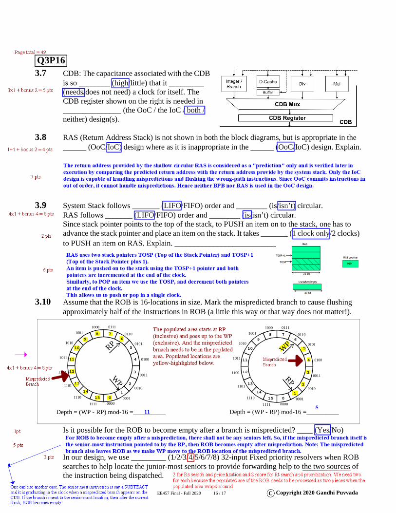
3.10 Assume that the ROB is 16-locations in size. Mark the mispredicted branch to cause flushing approximately half of the instructions in ROB (a little this way or that way does not matter!).
Is it possible for the ROB to become empty after a branch is mispredicted? ____ (Yes/No)Explain: _________________________________________________________________________________________________________________________________________________In our design, we use _________ (1/2/3/4/5/6/7/8) 32-input Fixed priority resolvers when ROB searches to help locate the junior-most seniors to provide forwarding help to the two sources of the instruction being dispatched.
01
2
3
4
5
678
9
10
11
12
13
14
15
RP
WP
00000001
0010
0011
0100
0101
0110
011110001001
1010
1011
1100
1101
1110
11110
1
2
3
4
5
678
9
10
11
12
13
14
15
RP
00000001
0010
0011
0100
0101
0110
011110001001
1010
1011
1100
1101
1110
1111
Depth = (WP - RP) mod-16 =__________ Depth = (WP - RP) mod-16 =__________
WP
Q3P16

EE457 Final - Fall 2020 17 / 17 C Copyright 2020 Gandhi Puvvada
4 ( points) min. CMP, Cache Coherency, CMT
4.1 In a ______________________ (blocking/non-blocking) cache, while the _______ (CCU/SCU) is fetching the missed block, the _______ (CCU/SCU) continues to serve other memory accessing instructions in (circle the right choices)(a) 1-Core 1-Thread CPU doing everything in-order (IoI-IoE-IoC)(b) 1-Core 1-Thread CPU doing out-of-order execution (IoI-OoE-IoC)(c) 1-Core 4-Thread in the core CPU doing in-order execution (IoI-IoE-IoC) for each thread(d) 4-Core each core1-Thread CPU doing everything in-order (IoI-IoE-IoC)
4.2 Since the "instruction" in MPI (miss rate per instruction) includes all instructions (not just the memory accessing instructions), an MPI of 5% is ____________ (easier/tougher) to achieve compared to the older specification of 95% cache hit rate where only memory accessing instructions are considered for the cache hit rate.In a system with a L1, L2, L3, and MM, L1 cache MPI is 10% and the L1 miss penalty is 10 clocks (i.e. L2 access time is 10 clocks) and L2 cache MPI is 5% and the L2 miss penalty is 50 clocks (i.e. L3 access time is 50 clocks) , and L3 cache MPI is 1% and the L3 miss penalty is 500 clocks (i.e. MM access time is 500 clocks) what is the overall CPI assuming there are no other problems causing lowering of the CPI. ________________________________________________________________________________________________________________________________________________________
4.3 In R/FMM, the R stands for replacement and the FMM stands for Flushing to the Main Memory.Write R/FMM or R/-- wherever appropriate in the diagrams below.
The left-side diagram for MSI protocol is for a ________ Write-back/Write-through cache.The right-side diagram for MOESI protocol is for a ________ Write-back/Write-through cache.Each of them could be used with direct-mapped or set-associative mapped caches. ______(T /F). TAG RAMs for cache following MSI protocol as compared to TAG RAMs following MOESI protocol are expected to be slightly ___________ (wider/narrower/same in width) and _______ (taller/shorter/same in height).
Q4P17