Embed Size (px)
Citation preview
1
EECS 427VLSI Design
Lecture 11: Dynamic Logic FamiliesProf. Pinaki Mazumder
Winter 2013
Adapted from Harris, Rabaey, Blaauw, Zhang, Sylvester, and others
Outline• Basic domino gate• Issues in dynamic gates• Domino cascading• Footless domino• NORA/Zipper logic• Multiple-output domino logic• Compound domino• Dual-rail domino• Self-reseting domino• Limited Switch dynamic logic

2
Domino / Static Cin/Cout
1
2 2 2
5
1
n
i
2
Φ
Static:Ci = 7Cn = 9
Dynamic:Ci = 2Cn = 7
Skew foreval
3-input OR gate
3
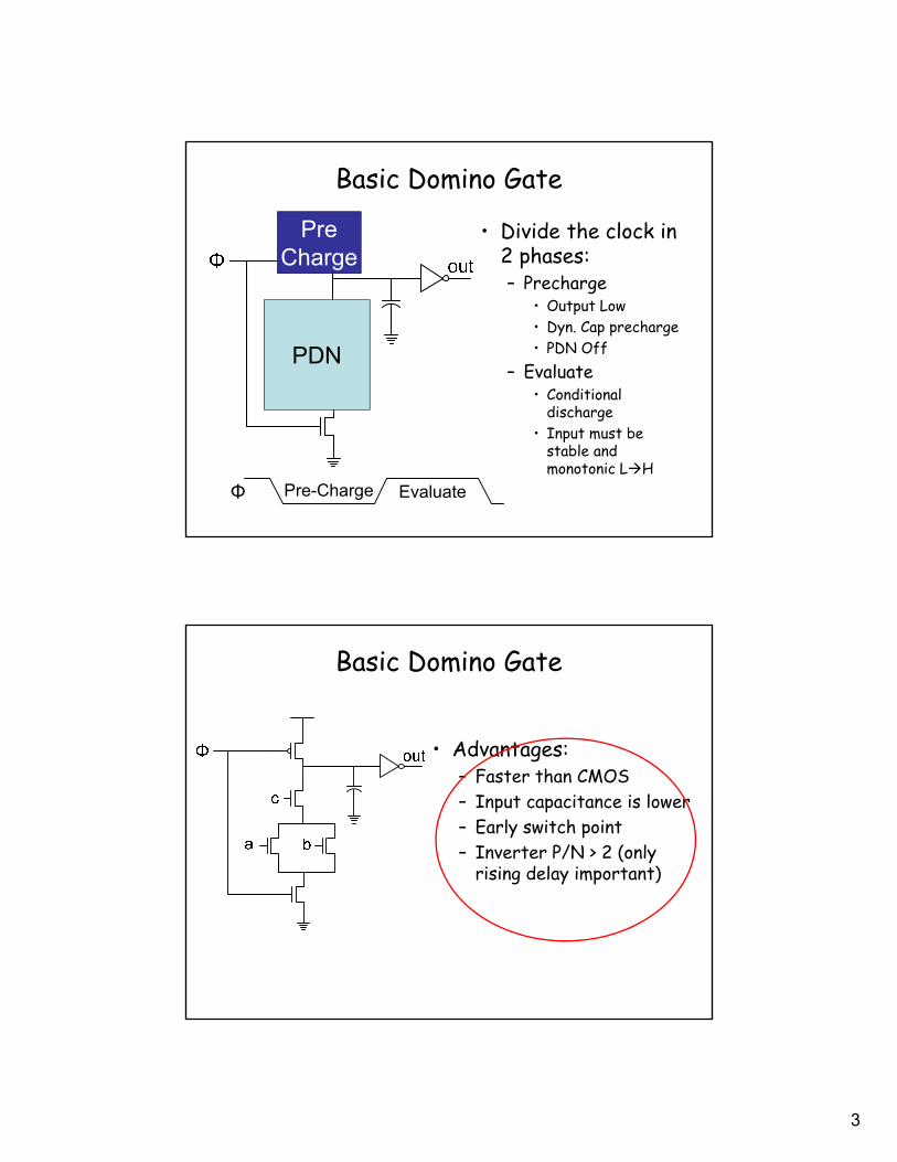
Basic Domino Gate
• Divide the clock in 2 phases:– Precharge
• Output Low• Dyn. Cap precharge• PDN Off
– Evaluate• Conditional
discharge• Input must be
stable and monotonic LH
PDN
PreCharge
Pre-Charge EvaluateΦ
Basic Domino Gate
• Advantages:– Faster than CMOS– Input capacitance is lower– Early switch point– Inverter P/N > 2 (only
rising delay important)
4
Basic Domino Gate
• Disadvantages:– Low noise margin– Charge sharing– Leakage currents– Internal capacitance
charge sensitive to noise
EE141© Digital Integrated Circuits2ndCombinational Circuits
8
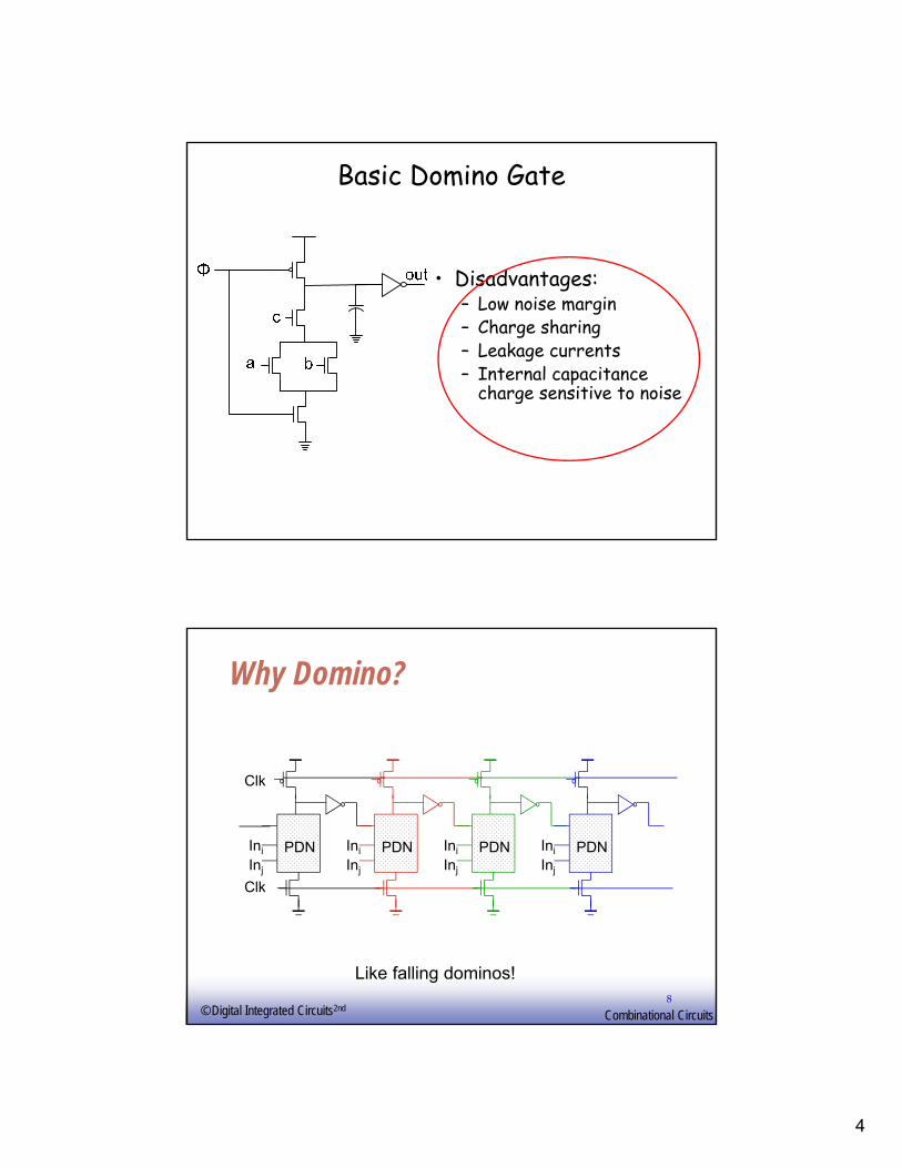
Why Domino?
Clk
Clk
Ini PDNInj
Ini
Inj
PDN Ini PDNInj
Ini PDNInj
Like falling dominos!

5
Φ1
Φ2
B
C
D
Φ
Footless Domino
E P E
E P
PE E
E
Evaluate before inputs validPrecharge after inputs precharge

6
EE141© Digital Integrated Circuits2ndCombinational Circuits
11
Dynamic CMOS
In static circuits at every point in time (except when switching) the output is connected to either GND or VDD via a low resistance path. fan-in of n requires 2n (n N-type + n P-type) devices
Dynamic circuits rely on the temporary storage of signal values on the capacitance of high impedance nodes. requires on n + 2 (n+1 N-type + 1 P-type) transistors
EE141© Digital Integrated Circuits2ndCombinational Circuits
12
Dynamic Gate
In1
In2 PDN
In3
Me
Mp
Clk
Clk
Out
CL
Out
Clk
Clk
A
BC
Mp
Me
Two phase operationPrecharge (CLK = 0)Evaluate (CLK = 1)
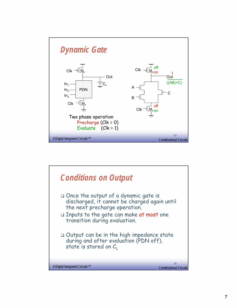
7
EE141© Digital Integrated Circuits2ndCombinational Circuits
13
Dynamic Gate
In1
In2 PDN
In3
Me
Mp
Clk
Clk
Out
CL
Out
Clk
Clk
A
BC
Mp
Me
Two phase operationPrecharge (Clk = 0)Evaluate (Clk = 1)
on
off
1
off
on
((AB)+C)
EE141© Digital Integrated Circuits2ndCombinational Circuits
14
Conditions on Output
Once the output of a dynamic gate is discharged, it cannot be charged again until the next precharge operation.
Inputs to the gate can make at most one transition during evaluation.
Output can be in the high impedance state during and after evaluation (PDN off), state is stored on CL
8
EE141© Digital Integrated Circuits2ndCombinational Circuits
15
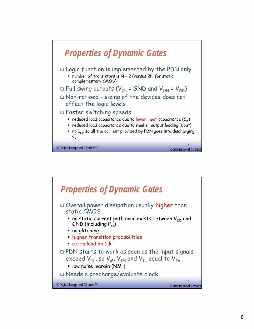
Properties of Dynamic Gates
Logic function is implemented by the PDN only number of transistors is N + 2 (versus 2N for static
complementary CMOS)
Full swing outputs (VOL = GND and VOH = VDD) Non-ratioed - sizing of the devices does not
affect the logic levels Faster switching speeds
reduced load capacitance due to lower input capacitance (Cin) reduced load capacitance due to smaller output loading (Cout) no Isc, so all the current provided by PDN goes into discharging
CL
EE141© Digital Integrated Circuits2ndCombinational Circuits
16
Properties of Dynamic Gates
Overall power dissipation usually higher than static CMOS no static current path ever exists between VDD and
GND (including Psc) no glitching higher transition probabilities extra load on Clk
PDN starts to work as soon as the input signals exceed VTn, so VM, VIH and VIL equal to VTn low noise margin (NML)
Needs a precharge/evaluate clock
9
EE141© Digital Integrated Circuits2ndCombinational Circuits
17
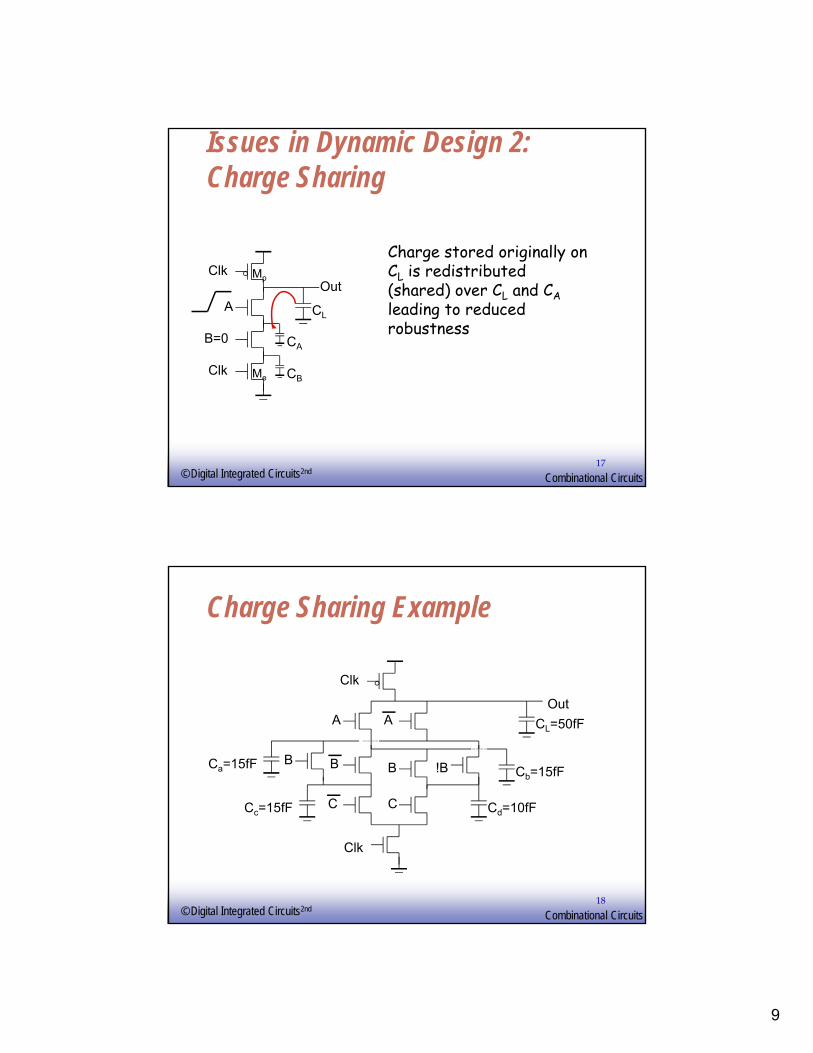
Issues in Dynamic Design 2: Charge Sharing
CL
Clk
Clk
CA
CB
B=0
A
OutMp
Me
Charge stored originally on CL is redistributed (shared) over CL and CAleading to reduced robustness
EE141© Digital Integrated Circuits2ndCombinational Circuits
18
Charge Sharing Example
CL=50fF
Clk
Clk
A A
B B B !B
CC
Out
Ca=15fF
Cc=15fF
Cb=15fF
Cd=10fF

10
EE141© Digital Integrated Circuits2ndCombinational Circuits
19
Charge Sharing
CLVDD CLVout t Ca VDD VTn VX – +=
or
Vout Vout t VDD–CaCL-------- VDD VTn VX – –= =
Vout VDD
CaCa CL+----------------------
–=
case 1) if Vout < VTn
case 2) if Vout > VTnB 0
Clk
X
CL
Ca
Cb
A
Out
Mp
Ma
VDD
Mb
Clk Me
EE141© Digital Integrated Circuits2ndCombinational Circuits
20
Solution to Charge Redistribution
Clk
Clk
Me
Mp
A
B
OutMkp
Clk
Precharge internal nodes using a clock-driven transistor (at the cost of increased area and power)

11
EE141© Digital Integrated Circuits2ndCombinational Circuits
21
Issues in Dynamic Design 3: Backgate Coupling
CL1
Clk
Clk
B=0
A=0
Out1Mp
Me
Out2
CL2In
Dynamic NAND
Static NAND
=1=0
EE141© Digital Integrated Circuits2ndCombinational Circuits
22
Backgate Coupling Effect
-1
0
1
2
3
0 2 4 6Time, ns
Clk
In
Out1
Out2
12
EE141© Digital Integrated Circuits2ndCombinational Circuits
23
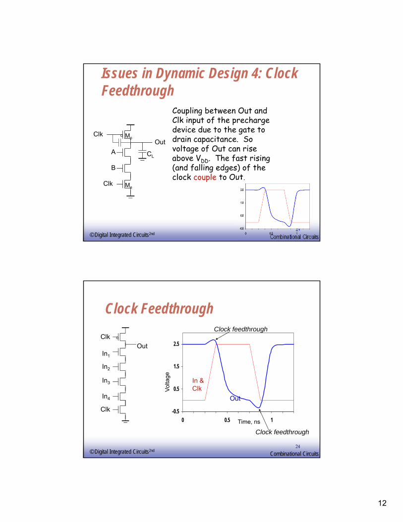
Issues in Dynamic Design 4: Clock Feedthrough
CL
Clk
Clk
B
A
OutMp
Me
Coupling between Out and Clk input of the precharge device due to the gate to drain capacitance. So voltage of Out can rise above VDD. The fast rising (and falling edges) of the clock couple to Out.
EE141© Digital Integrated Circuits2ndCombinational Circuits
24
Clock Feedthrough
-0.5
0.5
1.5
2.5
0 0.5 1
Clk
Clk
In1
In2
In3
In4
Out
In &Clk
Out
Time, ns
Clock feedthrough
Clock feedthrough
13
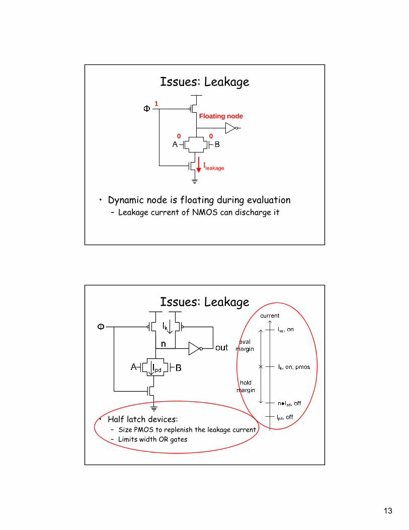
Issues: Leakage
• Dynamic node is floating during evaluation– Leakage current of NMOS can discharge it
Ileakage
1
0 0
Floating node
Issues: Leakage
• Half latch devices:– Size PMOS to replenish the leakage current– Limits width OR gates
14
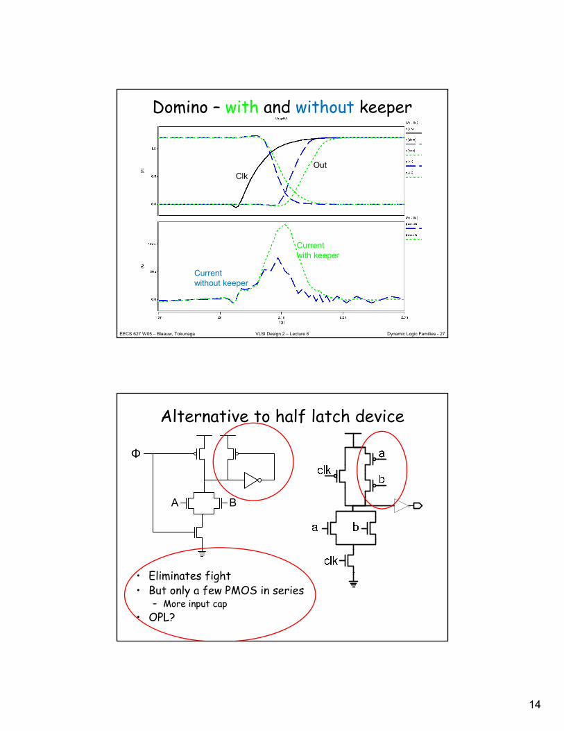
Dynamic Logic Families - 27EECS 627 W05 – Blaauw, Tokunaga VLSI Design 2 – Lecture 6
Domino – with and without keeper
Clk
Current with keeper
Currentwithout keeper
Out
Alternative to half latch device
A
Φ
B
• Eliminates fight• But only a few PMOS in series
– More input cap• OPL?
15
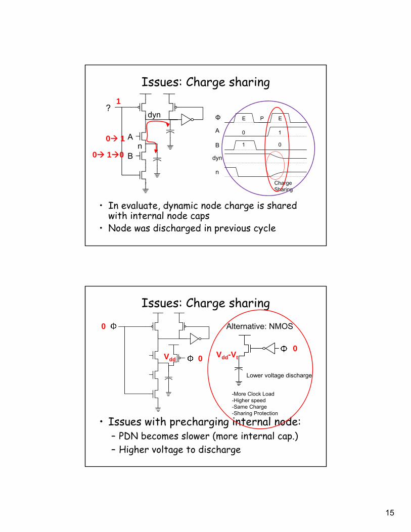
Issues: Charge sharing
• In evaluate, dynamic node charge is shared with internal node caps
• Node was discharged in previous cycle
1
Φ
A
B
n
dyn
?
A
Bn
dyn
0 1
0 10
ChargeSharing
E EP
0
1
1
0
Issues: Charge sharing
• Issues with precharging internal node:– PDN becomes slower (more internal cap.)– Higher voltage to discharge
0
0
Vdd
-More Clock Load-Higher speed-Same Charge-Sharing Protection
Alternative: NMOS
Vdd-Vt
0
Lower voltage discharge
16
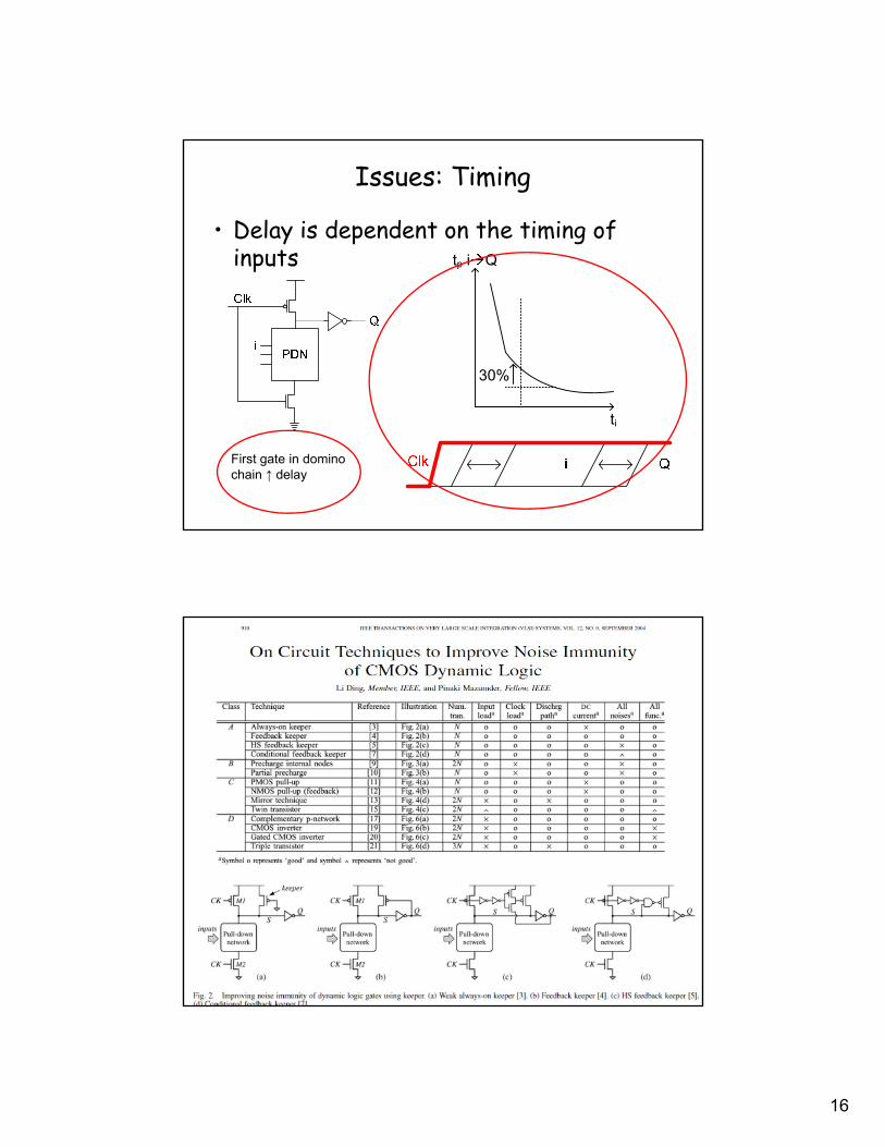
Issues: Timing
• Delay is dependent on the timing of inputs
First gate in dominochain ↑ delay
ti
tp i Q
30%
17
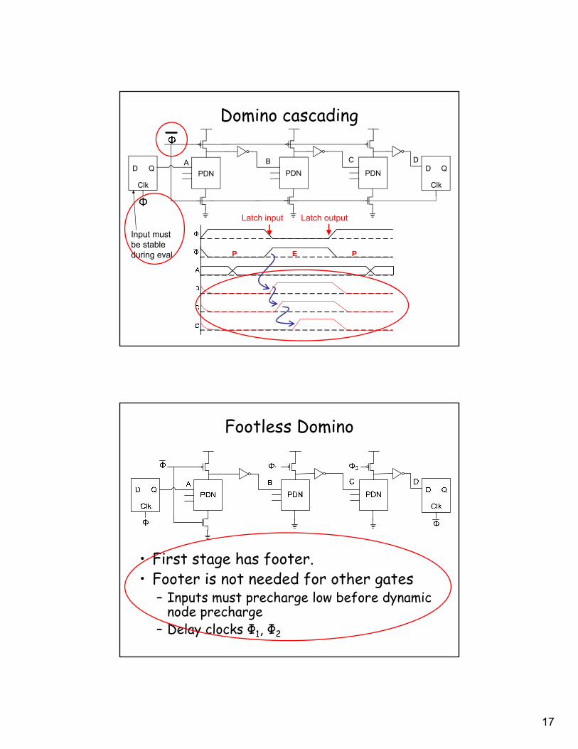
Domino cascading
P E P
Latch input Latch output
PDND Q
Clk
PDN PDND Q
Clk
A B C D
Φ
Input mustbe stableduring eval
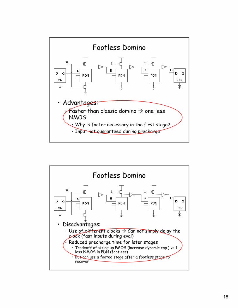
Footless Domino
• First stage has footer.• Footer is not needed for other gates
– Inputs must precharge low before dynamic node precharge
– Delay clocks Φ1, Φ2
18
Footless Domino
• Advantages:– Faster than classic domino one less
NMOS• Why is footer necessary in the first stage?• Input not guaranteed during precharge
Footless Domino
• Disadvantages:– Use of different clocks Can not simply delay the
clock (fast inputs during eval)– Reduced precharge time for later stages
• Tradeoff of sizing up PMOS (increase dynamic cap.) vs 1 less NMOS in PDN (footless)
• But can use a footed stage after a footless stage to recover

19
NORA/Zipper Logic
• Cascade basic dynamic gates with different evaluation networks (PDN, PUN)
Precharge High
Precharge Low
NORA/Zipper Logic
• Advantages:– Eliminates the inverter delay (but no drive for long
interconnect)– Fast

20
NORA/Zipper Logic
• Disadvantages:– Not very good for large output loads (Does not use an output
inverter)– Big and slow PMOS PUN– Bad noise margins Can add keeper– Noise on dynamic node– Cannot make arbitrary connections
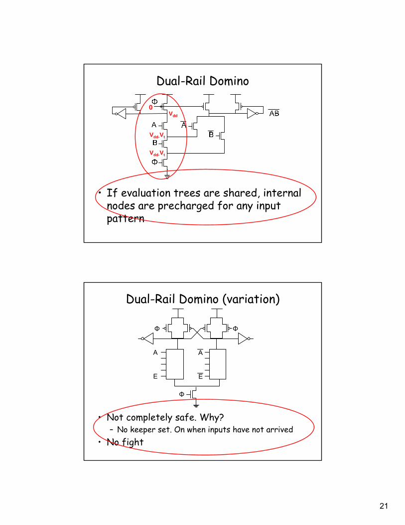
Dual-Rail Domino
• Only non-inverting gates in domino– Dual-rail is required for general logic
functions• Double the number of transistors
Why good?Always precharged
Shared Less clock loadOnly 1 tree evaluates
21
Dual-Rail Domino
0Vdd
Vdd-Vt
Vdd-Vt
• If evaluation trees are shared, internal nodes are precharged for any input pattern
Dual-Rail Domino (variation)
• Not completely safe. Why?– No keeper set. On when inputs have not arrived
• No fight
A
E
A
E
Φ Φ
Φ
22
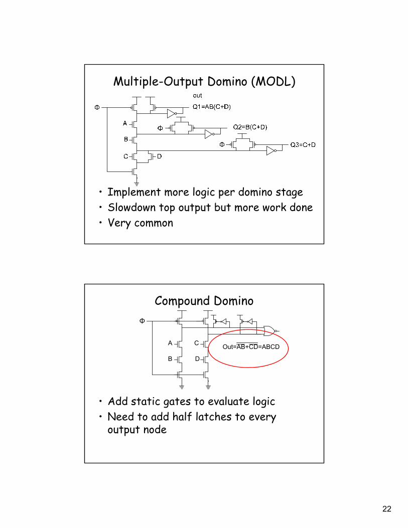
Multiple-Output Domino (MODL)
• Implement more logic per domino stage• Slowdown top output but more work done• Very common
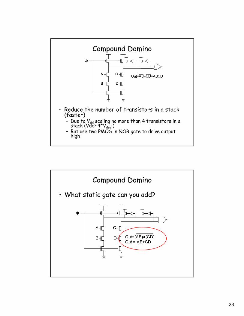
Compound Domino
• Add static gates to evaluate logic• Need to add half latches to every
output node
A
B
Φ
C
D
Out=AB+CD=ABCD
23
Compound Domino
• Reduce the number of transistors in a stack (faster)– Due to Vdd scaling no more than 4 transistors in a
stack (Vdd~4*Vdsat)– But use two PMOS in NOR gate to drive output
high
Compound Domino
• What static gate can you add?

24
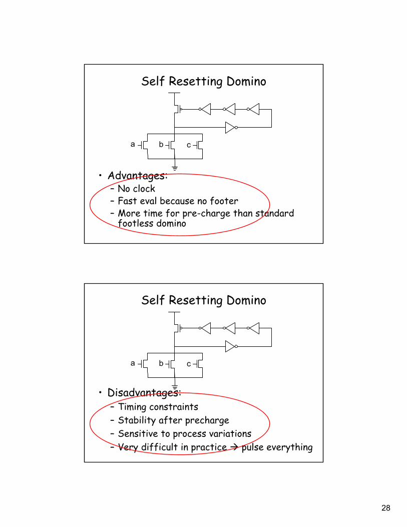
Self Resetting Domino
No footer
Non clockedprecharge.Prechargecontrolled byoutput
Self Resetting Domino
0 00
10
1
f
nout
Dynamic nodefloating

25
Self Resetting Domino
0 0
1
out
NO FIGHTPMOS OFF
a b c
f
n
Self Resetting Domino
0 0
1
1
01
out
f
n

26
Self Resetting Domino
0 00
Input must be precharged before pulse ripples through
a b c
f
n
Self Resetting Domino
0 00
10
f
n
27
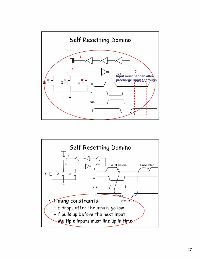
Self Resetting Domino
0 00
10
1
out
a b c
f
nInput must happen after precharge ripples through
• Timing constraints:– f drops after the inputs go low– f pulls up before the next input– Multiple inputs must line up in time
Self Resetting Domino
a b c
f
n out A fall before A rise after
precharge
28
Self Resetting Domino
• Advantages:– No clock– Fast eval because no footer– More time for pre-charge than standard
footless domino
a b c
Self Resetting Domino
• Disadvantages:– Timing constraints– Stability after precharge– Sensitive to process variations– Very difficult in practice pulse everything
a b c
29
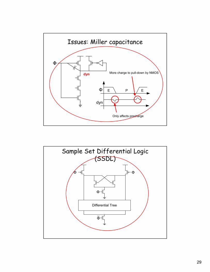
Issues: Miller capacitance
dyn
E P EΦ
dyn
More charge to pull-down by NMOS
Only affects precharge
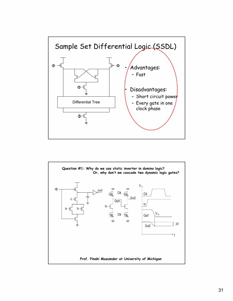
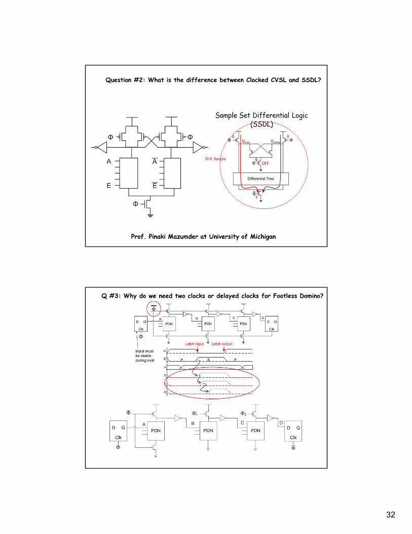
Sample Set Differential Logic (SSDL)
Differential Tree
Φ
Φ
Φ
Φ

30
Sample Set Differential Logic (SSDL)
Differential Tree
Φ
Φ
Φ
ΦΦ=0 Sample
0 0
0
1
OFF
Vtrue Vcomp
Sample Set Differential Logic (SSDL)
Differential Tree
Φ
Φ
Φ
ΦΦ=1 Amplify
1 1
0
ON
Vtrue Vcomp
31
Sample Set Differential Logic (SSDL)
• Advantages:– Fast
• Disadvantages:– Short circuit power– Every gate in one
clock phaseDifferential Tree
Φ
Φ
Φ
Φ
Question #1: Why do we use static inverter in domino logic? Or, why don’t we cascade two dynamic logic gates?
Prof. Pinaki Mazumder at University of Michigan
32
Question #2: What is the difference between Clocked CVSL and SSDL?
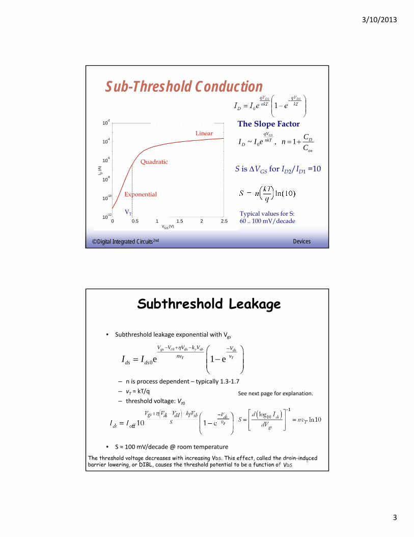
Q #3: Why do we need two clocks or delayed clocks for Footless Domino?

3/10/2013
1
Lecture 12 –Static Power
WH 5.3
Adapted from Weste & Harris, and Rabaey & Chandrakashan
Prof. Pinaki Mazumder
1
Topics
• Leakage mechanisms– Subthreshold leakage– Gate oxide leakage
• Leakage reduction methods– State assignment– MTCMOS– Dual-Vth design– VTCMOS

3/10/2013
2
Leakage mechanisms
• I1: Reverse-bias p-n junction– Reverse-biased p-n junctions current: – Typically < 1 fA/mm2 (negligible)– Depends on area and perimeter of diffusion
regions– Also: Band to Band tunneling (BTBT)
n+
P-sub
Vdd
n+
I1
e 1D
T
V
vD SI I
Leakage mechanisms
• I2: Weak inversion or subthresholdleakage current– Increased voltage increases drain depletion
extending to the source lowers the potential barrier
– Dominant effect in modern devices
n+
P-sub
Vdd
n+I2
3/10/2013
3
© Digital Integrated Circuits2nd Devices
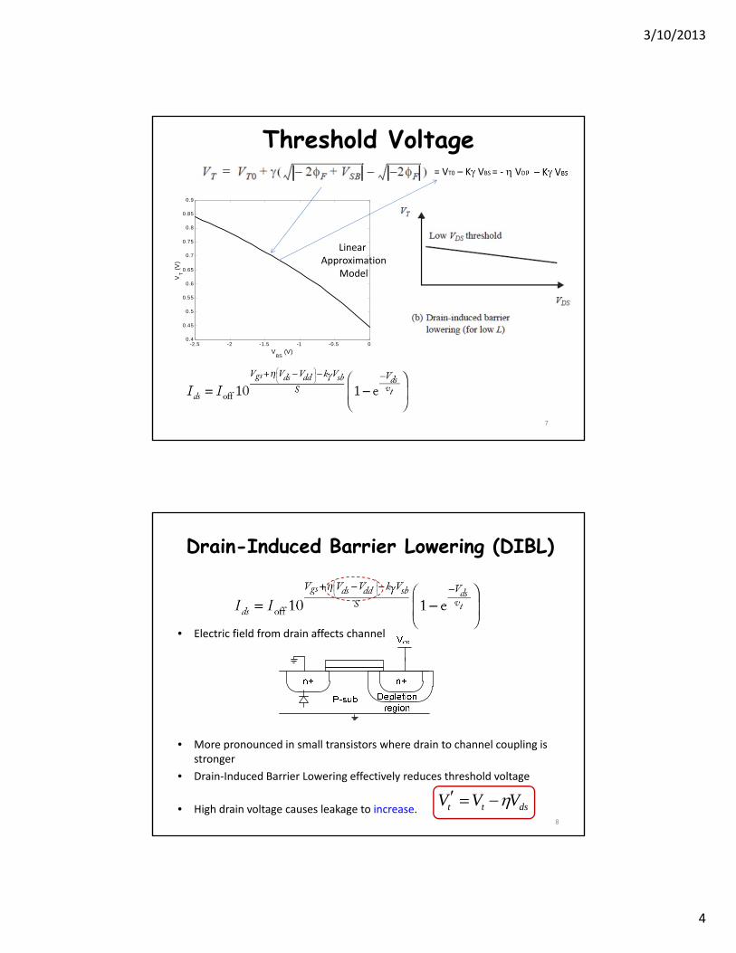
Sub-Threshold Conduction
0 0.5 1 1.5 2 2.510
-12
10-10
10-8
10-6
10-4
10-2
VGS (V)
I D(A
)
VT
Linear
Exponential
Quadratic
Typical values for S:60 .. 100 mV/decade
The Slope Factor
ox
DnkT
qV
D C
CneII
GS
1 ,~ 0
S is VGS for ID2/ID1 =10
vT
Subthreshold Leakage
• Subthreshold leakage exponential with Vgs
– n is process dependent – typically 1.3‐1.7
– vT = kT/q
– threshold voltage: Vt0
• Rewrite relative to Ioff on log scale
• S ≈ 100 mV/decade @ room temperature
0
0e 1 egs t ds sb ds
T T
V V V k V V
nv vds dsI I
6The threshold voltage decreases with increasing VDS. This effect, called the drain-induced barrier lowering, or DIBL, causes the threshold potential to be a function of
See next page for explanation.
3/10/2013
4
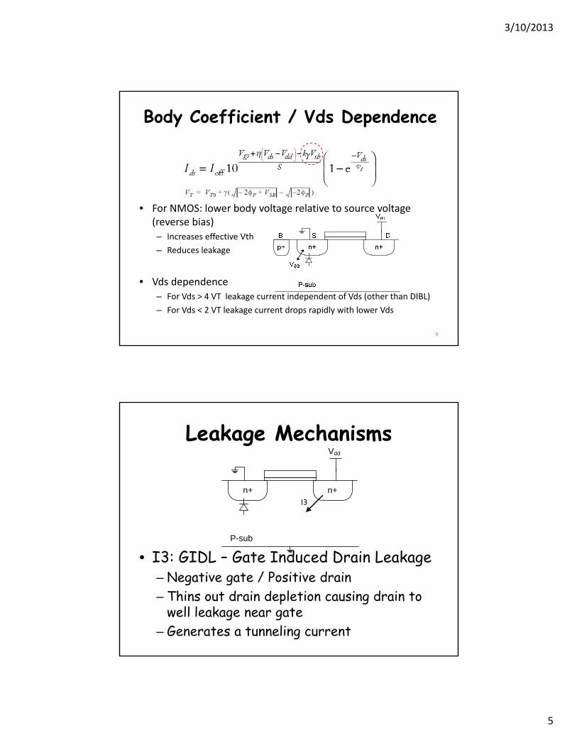
Threshold Voltage
7
-2.5 -2 -1.5 -1 -0.5 00.4
0.45
0.5
0.55
0.6
0.65
0.7
0.75
0.8
0.85
0.9
VBS
(V)
VT (
V)
= VT0 – K VBS = ‐ VDD
Linear Approximation
Model
Drain-Induced Barrier Lowering (DIBL)
• Electric field from drain affects channel
• More pronounced in small transistors where drain to channel coupling is stronger
• Drain‐Induced Barrier Lowering effectively reduces threshold voltage
• High drain voltage causes leakage to increase. t t dsV V V 8
3/10/2013
5
Body Coefficient / Vds Dependence
• For NMOS: lower body voltage relative to source voltage (reverse bias)– Increases effective Vth
– Reduces leakage
• Vds dependence– For Vds > 4 VT leakage current independent of Vds (other than DIBL)
– For Vds < 2 VT leakage current drops rapidly with lower Vds
9
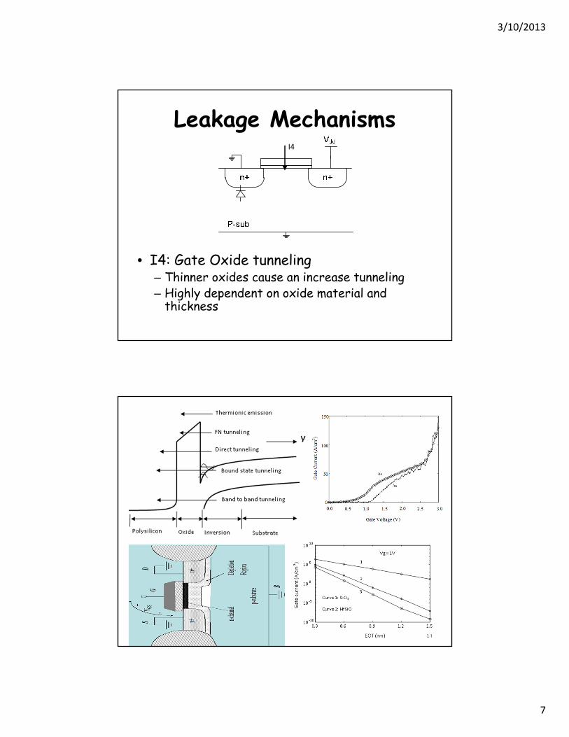
Leakage Mechanisms
• I3: GIDL – Gate Induced Drain Leakage– Negative gate / Positive drain– Thins out drain depletion causing drain to
well leakage near gate– Generates a tunneling current
n+
P-sub
Vdd
n+I3
3/10/2013
6
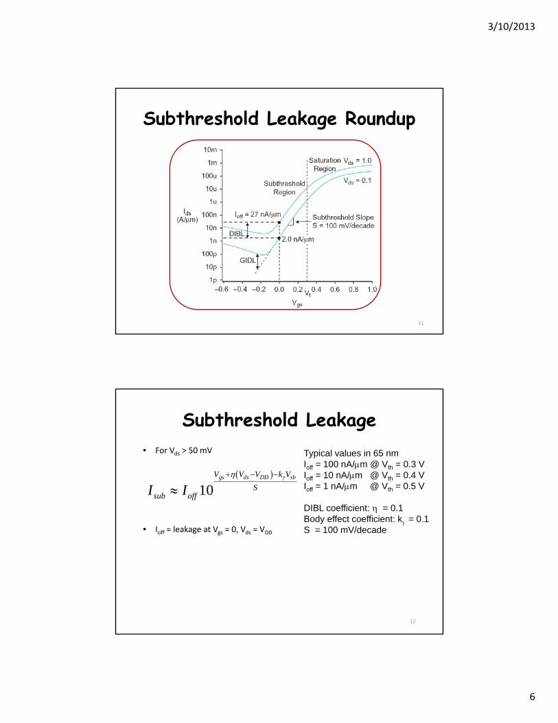
Subthreshold Leakage Roundup
11
Subthreshold Leakage• For Vds > 50 mV
• Ioff = leakage at Vgs = 0, Vds = VDD
10gs ds DD sbV V V k V
Ssub offI I
Typical values in 65 nmIoff = 100 nA/m @ Vth = 0.3 VIoff = 10 nA/m @ Vth = 0.4 VIoff = 1 nA/m @ Vth = 0.5 V
DIBL coefficient: = 0.1Body effect coefficient: k = 0.1S = 100 mV/decade
12
3/10/2013
7
Leakage Mechanisms
• I4: Gate Oxide tunneling– Thinner oxides cause an increase tunneling– Highly dependent on oxide material and
thickness
I4
14
3/10/2013
8
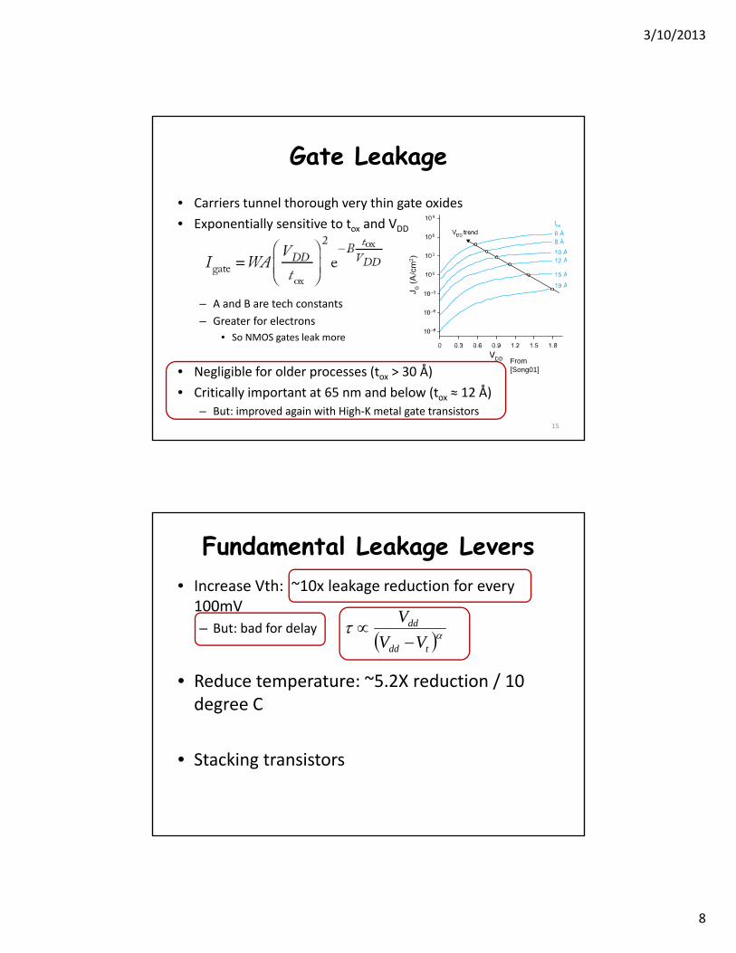
Gate Leakage
• Carriers tunnel thorough very thin gate oxides
• Exponentially sensitive to tox and VDD
– A and B are tech constants
– Greater for electrons
• So NMOS gates leak more
• Negligible for older processes (tox > 30 Å)
• Critically important at 65 nm and below (tox ≈ 12 Å)– But: improved again with High‐K metal gate transistors
From [Song01]
15
Fundamental Leakage Levers• Increase Vth: ~10x leakage reduction for every 100mV
– But: bad for delay
• Reduce temperature: ~5.2X reduction / 10 degree C
• Stacking transistors
tdd
dd
VV
V
3/10/2013
9
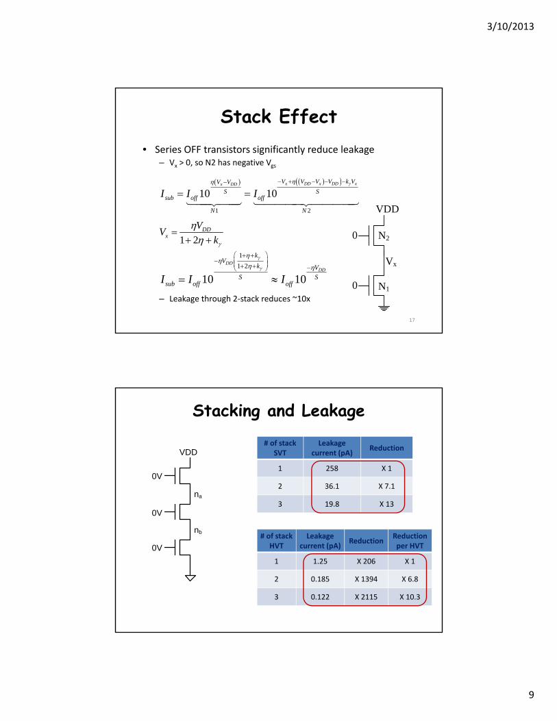
Stack Effect• Series OFF transistors significantly reduce leakage
– Vx > 0, so N2 has negative Vgs
– Leakage through 2‐stack reduces ~10x
1 2
10 10x DD x DD xx DD V V V V k VV V
S Ssub off off
N N
I I I
1 2DD
x
VV
k
1
1 2
10 10
DDDD
kV
k V
S Ssub off offI I I
17
N20
0
VDD
N1
Vx
Stacking and Leakage
0V
na
nb
0V
0V
VDD# of stack
SVTLeakage
current (pA)Reduction
1 258 X 1
2 36.1 X 7.1
3 19.8 X 13
# of stackHVT
Leakage current (pA)
ReductionReduction per HVT
1 1.25 X 206 X 1
2 0.185 X 1394 X 6.8
3 0.122 X 2115 X 10.3
3/10/2013
10
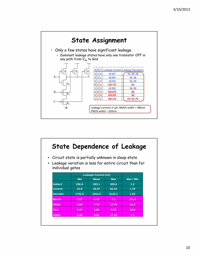
State Assignment
A B C Leakage Current Leaking Transistors
0 0 0 10.537 N1, N2, N3
0 0 1 18.534 N1, N2
0 1 0 18.234 N1, N3
0 1 1 135.772 N1
1 0 0 20.350 N2, N3
1 0 1 102.672 N21 1 0 100.970 N3
1 1 1 192.174 P1, P2, P3
• Only a few states have significant leakage– Dominant leakage states have only one transistor OFF in
any path from Vdd to Gnd
N2
N1
N3
P1 P2 P3
A
B
C
Leakage currents in pA. NMOS width = 480nmPMOS width = 320nm
State Dependence of Leakage• Circuit state is partially unknown in sleep state• Leakage variation is less for entire circuit than for
individual gates
Min Mean Max
Adder1 256.8 283.1 309.8 1.2
Control 33.8 45.97 60.23 1.78
Decoder 1702.5 1914.3 2122.1 1.25
Nand4 0.07 0.76 7.1 101.4
OAI21 0.84 7.73 17.78 21.2
Tinv 0.37 1.89 5.76 15.6
AOI21 2.44 8.51 17.23 7.1
Leakage Current (nA)
Max / Min
3/10/2013
11
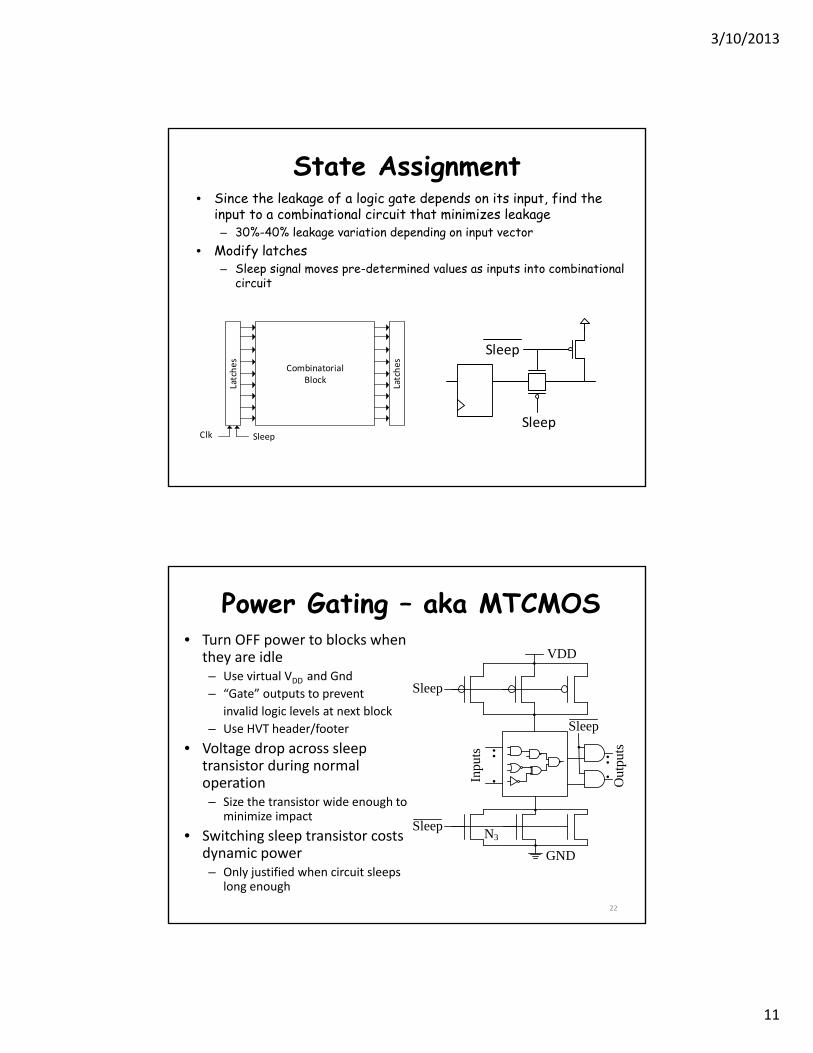
State Assignment• Since the leakage of a logic gate depends on its input, find the
input to a combinational circuit that minimizes leakage– 30%-40% leakage variation depending on input vector
• Modify latches– Sleep signal moves pre-determined values as inputs into combinational
circuit
CombinatorialBlock
Latches
Latches
Clk Sleep
Sleep
Sleep
Power Gating – aka MTCMOS• Turn OFF power to blocks when
they are idle– Use virtual VDD and Gnd
– “Gate” outputs to prevent
invalid logic levels at next block
– Use HVT header/footer
• Voltage drop across sleep transistor during normal operation– Size the transistor wide enough to
minimize impact
• Switching sleep transistor costs dynamic power– Only justified when circuit sleeps
long enough
22
N3
Sleep
Sleep
Inpu
ts
Sleep
Out
puts
VDD
GND
3/10/2013
12
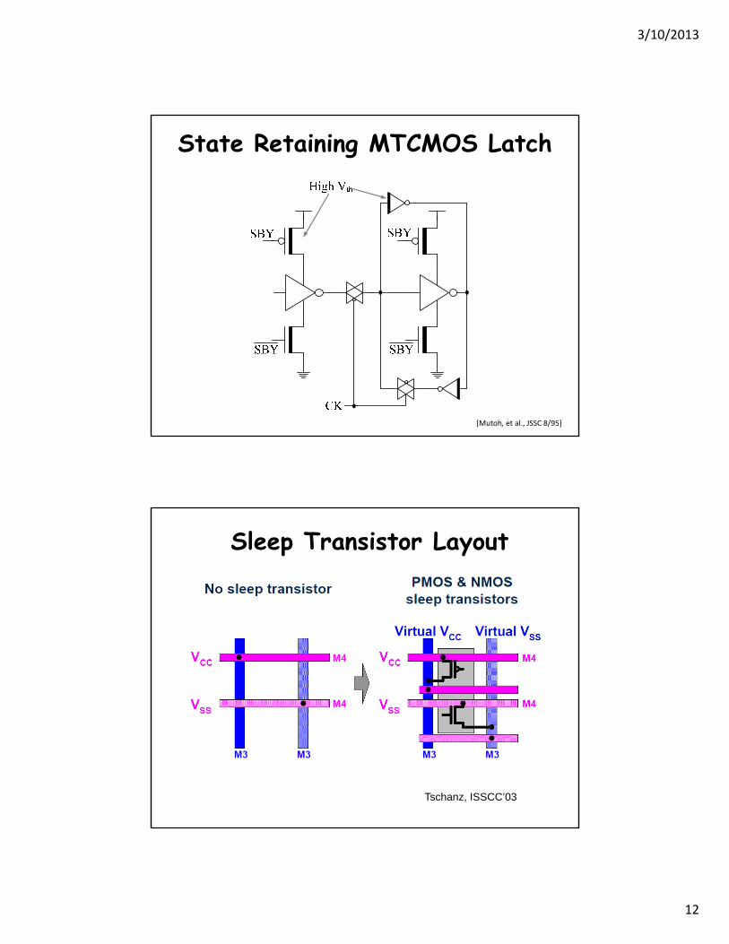
State Retaining MTCMOS Latch
[Mutoh, et al., JSSC 8/95]
Sleep Transistor Layout
Tschanz, ISSCC’03

3/10/2013
13
Dual-Thresholds Inside a Logic Block• Minimum energy consumption is achieved if all logic paths
are critical (have the same delay)• Use lower threshold on timing-critical paths
– Assignment can be done on a per gate or transistor basis; no clustering of logic is needed
– No level converters needed
Vth Assignment Granularity• Vth assignment can be performed at different levels
of granularity– Gate level assignment– Pull up network / Pull down network based assignment (half
gate)• Single Vth in pull up or pull down networks
– Stack based assignment• Single Vth in series connected transistors
– Individually assignment within transistor stacks
• Possible area penalty (see right)
• Number of library cells increases with finer control– Better leakage / delay trade-off– Harder for synthesis tools to handle
Design rule constraint for
different Vt assignment

3/10/2013
14
Dynamic Body Bias
Active modeForward body bias
Idle modeReverse body biasTriple well needed
Variable Threshold CMOS (VTCMOS)
N‐isolation
P‐sub
N‐well P‐well
VBBP VDD VSS VBBN
p+ p+ n+ n+
VDD
VSS
VBBP
VBBN
3/10/2013
15
29
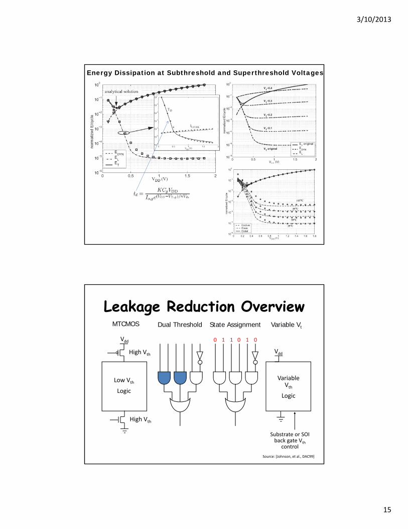
Energy Dissipation at Subthreshold and Superthreshold Voltages
Leakage Reduction Overview
Low Vth
Logic
High Vth
High Vth
Vdd
MTCMOS
Vdd
Variable Vth
Logic
Substrate or SOI back gate Vth
control
Variable VtDual Threshold State Assignment
0 1 1 0 1 0
Source: [Johnson, et al., DAC99]
3/10/2013
16
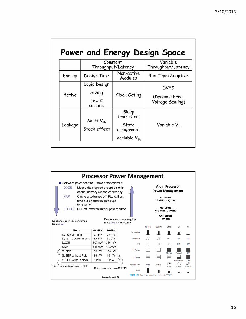
Power and Energy Design SpaceConstant
Throughput/LatencyVariable
Throughput/Latency
Energy Design Time Non-active Modules Run Time/Adaptive
Active
Logic Design
Sizing
Low C circuits
Clock GatingDVFS
(Dynamic Freq, Voltage Scaling)
LeakageMulti-Vth
Stack effect
Sleep Transistors
State assignment
Variable Vth
Variable Vth
32
Processor Power Management
Atom ProcessorPower Management
3/10/2013
17
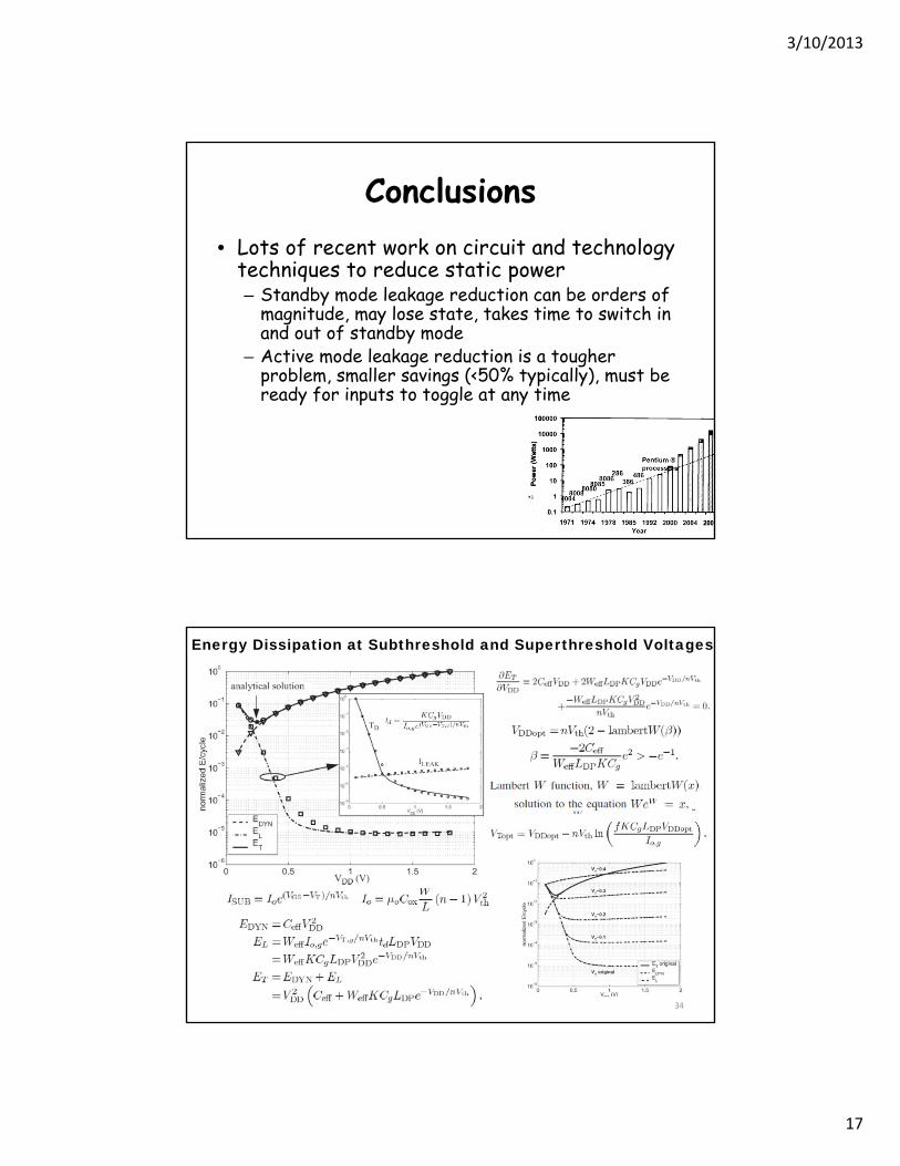
Conclusions• Lots of recent work on circuit and technology
techniques to reduce static power– Standby mode leakage reduction can be orders of
magnitude, may lose state, takes time to switch in and out of standby mode
– Active mode leakage reduction is a tougher problem, smaller savings (<50% typically), must be ready for inputs to toggle at any time
33
34
Energy Dissipation at Subthreshold and Superthreshold Voltages