Embed Size (px)
Citation preview
Effect of crystalline/amorphous interfaces on thermal transport across confined thinfilms and superlatticesAshutosh Giri, Jeffrey L. Braun, and Patrick E. Hopkins Citation: Journal of Applied Physics 119, 235305 (2016); doi: 10.1063/1.4953683 View online: http://dx.doi.org/10.1063/1.4953683 View Table of Contents: http://scitation.aip.org/content/aip/journal/jap/119/23?ver=pdfcov Published by the AIP Publishing Articles you may be interested in Crystalline-amorphous silicon nano-composites: Nano-pores and nano-inclusions impact on the thermalconductivity J. Appl. Phys. 119, 175104 (2016); 10.1063/1.4948337 Optical bandgap of single- and multi-layered amorphous germanium ultra-thin films J. Appl. Phys. 119, 014304 (2016); 10.1063/1.4939296 Lattice thermal conductivity of crystalline and amorphous silicon with and without isotopic effects from the ballisticto diffusive thermal transport regime J. Appl. Phys. 116, 043514 (2014); 10.1063/1.4891500 Effect of film thickness on the thermal resistance of confined semiconductor thin films J. Appl. Phys. 107, 013521 (2010); 10.1063/1.3275506 Interfacial effects on the thermal conductivity of a -Ge thin films grown on Si substrates J. Appl. Phys. 104, 074903 (2008); 10.1063/1.2986443
Reuse of AIP Publishing content is subject to the terms at: https://publishing.aip.org/authors/rights-and-permissions. Download to IP: 137.54.2.234 On: Thu, 16 Jun 2016
15:32:07
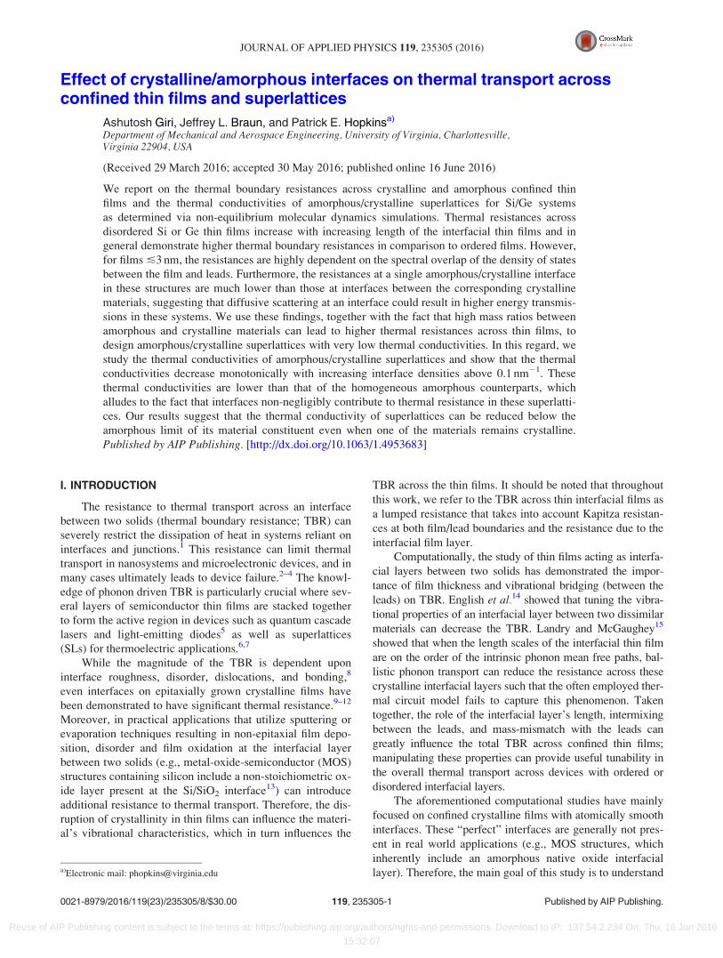
Effect of crystalline/amorphous interfaces on thermal transport acrossconfined thin films and superlattices
Ashutosh Giri, Jeffrey L. Braun, and Patrick E. Hopkinsa)
Department of Mechanical and Aerospace Engineering, University of Virginia, Charlottesville,Virginia 22904, USA
(Received 29 March 2016; accepted 30 May 2016; published online 16 June 2016)
We report on the thermal boundary resistances across crystalline and amorphous confined thin
films and the thermal conductivities of amorphous/crystalline superlattices for Si/Ge systems
as determined via non-equilibrium molecular dynamics simulations. Thermal resistances across
disordered Si or Ge thin films increase with increasing length of the interfacial thin films and in
general demonstrate higher thermal boundary resistances in comparison to ordered films. However,
for films �3 nm, the resistances are highly dependent on the spectral overlap of the density of states
between the film and leads. Furthermore, the resistances at a single amorphous/crystalline interface
in these structures are much lower than those at interfaces between the corresponding crystalline
materials, suggesting that diffusive scattering at an interface could result in higher energy transmis-
sions in these systems. We use these findings, together with the fact that high mass ratios between
amorphous and crystalline materials can lead to higher thermal resistances across thin films, to
design amorphous/crystalline superlattices with very low thermal conductivities. In this regard, we
study the thermal conductivities of amorphous/crystalline superlattices and show that the thermal
conductivities decrease monotonically with increasing interface densities above 0.1 nm�1. These
thermal conductivities are lower than that of the homogeneous amorphous counterparts, which
alludes to the fact that interfaces non-negligibly contribute to thermal resistance in these superlatti-
ces. Our results suggest that the thermal conductivity of superlattices can be reduced below the
amorphous limit of its material constituent even when one of the materials remains crystalline.
Published by AIP Publishing. [http://dx.doi.org/10.1063/1.4953683]
I. INTRODUCTION
The resistance to thermal transport across an interface
between two solids (thermal boundary resistance; TBR) can
severely restrict the dissipation of heat in systems reliant on
interfaces and junctions.1 This resistance can limit thermal
transport in nanosystems and microelectronic devices, and in
many cases ultimately leads to device failure.2–4 The knowl-
edge of phonon driven TBR is particularly crucial where sev-
eral layers of semiconductor thin films are stacked together
to form the active region in devices such as quantum cascade
lasers and light-emitting diodes5 as well as superlattices
(SLs) for thermoelectric applications.6,7
While the magnitude of the TBR is dependent upon
interface roughness, disorder, dislocations, and bonding,8
even interfaces on epitaxially grown crystalline films have
been demonstrated to have significant thermal resistance.9–12
Moreover, in practical applications that utilize sputtering or
evaporation techniques resulting in non-epitaxial film depo-
sition, disorder and film oxidation at the interfacial layer
between two solids (e.g., metal-oxide-semiconductor (MOS)
structures containing silicon include a non-stoichiometric ox-
ide layer present at the Si/SiO2 interface13) can introduce
additional resistance to thermal transport. Therefore, the dis-
ruption of crystallinity in thin films can influence the materi-
al’s vibrational characteristics, which in turn influences the
TBR across the thin films. It should be noted that throughout
this work, we refer to the TBR across thin interfacial films as
a lumped resistance that takes into account Kapitza resistan-
ces at both film/lead boundaries and the resistance due to the
interfacial film layer.
Computationally, the study of thin films acting as interfa-
cial layers between two solids has demonstrated the impor-
tance of film thickness and vibrational bridging (between the
leads) on TBR. English et al.14 showed that tuning the vibra-
tional properties of an interfacial layer between two dissimilar
materials can decrease the TBR. Landry and McGaughey15
showed that when the length scales of the interfacial thin film
are on the order of the intrinsic phonon mean free paths, bal-
listic phonon transport can reduce the resistance across these
crystalline interfacial layers such that the often employed ther-
mal circuit model fails to capture this phenomenon. Taken
together, the role of the interfacial layer’s length, intermixing
between the leads, and mass-mismatch with the leads can
greatly influence the total TBR across confined thin films;
manipulating these properties can provide useful tunability in
the overall thermal transport across devices with ordered or
disordered interfacial layers.
The aforementioned computational studies have mainly
focused on confined crystalline films with atomically smooth
interfaces. These “perfect” interfaces are generally not pres-
ent in real world applications (e.g., MOS structures, which
inherently include an amorphous native oxide interfacial
layer). Therefore, the main goal of this study is to understanda)Electronic mail: [email protected]
0021-8979/2016/119(23)/235305/8/$30.00 Published by AIP Publishing.119, 235305-1
JOURNAL OF APPLIED PHYSICS 119, 235305 (2016)
Reuse of AIP Publishing content is subject to the terms at: https://publishing.aip.org/authors/rights-and-permissions. Download to IP: 137.54.2.234 On: Thu, 16 Jun 2016
15:32:07
the role of amorphous interfacial layers and the effect of
mass and thickness of these layers on the TBR.
Generally speaking, pristine interfaces are considered
ideal for interfacial heat flow, and diffusive scattering caused
by disruption of crystallinity in the vicinity of interfaces is
usually thought to impede thermal transport. In this regard,
we also seek to understand the contribution of the individual
lead/film resistances on the total TBR across amorphous
interfacial layers. Finally, we also seek to design amorphous/
crystalline superlattices (SLs) with high interface densities
where the resistances across the amorphous/crystalline inter-
faces non-negligibly contribute to lowering the thermal
conductivities of these structures (even beyond that of the
amorphous counterpart). For these purposes, in this work, we
systematically investigate the combined role of disorder,
mass-mismatch, and layer length on thermal transport across
thin confined films and amorphous/crystalline SLs using mo-
lecular dynamics (MD) simulations.
For lattice-mismatched crystalline films confined
between two crystalline leads, we find that ballistic trans-
port across Ge/Si/Ge structures and diffusive transport
across Si/Ge/Si structures affect the TBR across the respec-
tive interfacial regions, similar to the findings of Landry
and McGaughey16 for lattice-matched Si/Ge structures. In
contrast, the TBR across amorphous confined films is
shown to monotonically increase with film thickness,
regardless of the leads or the material comprising the amor-
phous film. Furthermore, for amorphous films with thick-
nesses �3 nm, we demonstrate that the spectral overlap in
the vibrational density of states between the leads and the
thin films can significantly affect the scattering of the pho-
non flux impinging upon the interfacial layer from the crys-
talline leads. Interestingly, we also find that the resistance
across a single amorphous/crystalline interface is lower
than that across the crystalline/crystalline counterpart.
These findings suggest that careful manipulation of the
vibrational properties of the disordered confined thin film
could lead to reduced TBR in comparison to the case where
the interface is comprised of two crystalline materials.
The results from our original goal mentioned in the
previous paragraph led us to design amorphous/crystalline
SLs that demonstrate very low thermal conductivities in the
second part of our study. More specifically, we utilize the
fact that crystalline/crystalline interfaces can demonstrate
higher TBRs compared to amorphous/crystalline interfaces
in designing SL structures with very low overall thermal
conductivities. In this regard, the main motivation in
designing these SLs is driven by the push towards achiev-
ing ultralow thermal conductivities (beyond the amorphous
limit to thermal conductivity of a material17) for applica-
tions such as thermal barrier coatings and thermoelectric
power generation.3 Several groups have overcome the
amorphous thermal conductivity limit by nanostructuring
and utilizing multilayered systems with high density of
interfaces.18–22 Consequently, it has been shown that varia-
tion in length scale in multilayered systems such as semi-
conductor superlattices (SLs) can shift phonon behavior
from a coherent, wave-like nature in which phonons tra-
verse the structure without scattering at internal interfaces
to an incoherent, particle-like nature in which scattering of
vibrational energy at interfaces can severely limit thermal
transport in SLs.23–26 As a result, computational studies
have predicted that crystalline superlattices can possess
lower thermal conductivities compared to that of their con-
stituent components.27–29 This is particularly significant in
Si-based SLs, where a significant amount of heat is carried
by phonons with long mean-free-paths.30–33
Along with the motivation of designing SLs with very
low thermal conductivities, our objective for the second part
of this study is also driven by the lack of attention given
towards understanding thermal transport across SLs compris-
ing of alternating amorphous/crystalline layers (that result
due to large lattice mismatch between constituent materi-
als)34 due to the generalization that in amorphous systems,
amorphicity is expected to dominate thermal transport while
interfaces do not pose as significant resistors.35,36 While
the understanding of thermal transport across amorphous/
crystalline heterojunctions has been limited, there has been
realization of such heterojunctions as potential materials for
solar cell and various photo-electronic device applica-
tions.37–39 Therefore, in the second part of our study, we
investigate the effect of layer thickness and mass-mismatch
on thermal conductivity in Si/Ge-based amorphous/crystal-
line superlattices. For these superlattices, we show that the
introduction of interfacial densities �0.1 nm�1 can severely
hinder thermal transport to result in thermal conductivities
even below that of the amorphous constituent comprising the
SL. Moreover, we do not observe size effects in the thermal
conductivities of these amorphous/crystalline superlattices,
which is in contrast to the size dependent thermal conductiv-
ities of crystalline/crystalline superlattices.40 This implies
that at interface densities �0.1 nm�1, vibrational transport in
these structures is dictated by incoherent boundary scattering
effects. We also show that by making use of the fact that the
resistance across a crystalline/crystalline interface can be
greater than at an amorphous/amorphous interface, the ther-
mal conductivities of these superlattices can be lowered by
as much as 10% by creating superlattice periods that consist
of two adjacent crystalline layers followed by two adjacent
amorphous layers. Finally, when comparing our results of
mass-mismatched crystalline/amorphous SLs to that of
amorphous/amorphous SLs, we find that at very high mass
ratios between the adjacent layers in the SLs, the thermal
conductivities are similar for the two different structures
(regardless of crystallinity in the amorphous/crystalline SL),
indicating the strong role of interfacial resistances in SLs
with large mismatch in the vibrational density of states
between the layers.
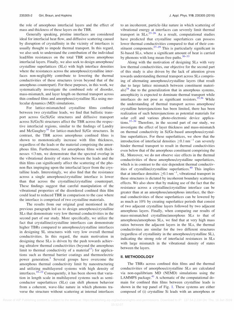
II. METHODOLOGY
The TBRs across confined thin films and the thermal
conductivities of amorphous/crystalline SLs are calculated
via non-equilibrium MD (NEMD) simulations using the
LAMMPS package.41 A schematic of the computational do-
main for confined thin films between crystalline leads is
shown in the top panel of Fig. 1. These systems are either
composed of (i) crystalline Si leads with an amorphous or
235305-2 Giri, Braun, and Hopkins J. Appl. Phys. 119, 235305 (2016)
Reuse of AIP Publishing content is subject to the terms at: https://publishing.aip.org/authors/rights-and-permissions. Download to IP: 137.54.2.234 On: Thu, 16 Jun 2016
15:32:07
crystalline layer of Ge in-between the leads or (ii) crystalline
Ge leads with an amorphous or crystalline layer of Si in-
between the leads. The Si-Si, Ge-Ge, and Si-Ge interatomic
potentials are described by the Tersoff potential,42,43 which
accounts for the strain associated with the lattice mismatch
at a Si/Ge interface.43 All simulations for these systems are
performed at an average temperature of 500 K, where elastic
scattering has been shown to dominate the TBR.16 We apply
fixed boundary conditions on the z-direction by fixing 4
monolayers of atoms that border the hot and cold reservoirs
as shown in the top panel of Fig. 1. Periodic boundary condi-
tions are applied in the x- and y-directions. The leads are
each 400 monolayers, and the cross section area Ac of the
simulation domain is set to five unit cells by five unit cells.
Based on previous MD simulations on similar Si/Ge systems,
we do not expect size effects to affect our MD-predicted
TBRs.15,16 A time step 0.5 fs is applied throughout the simu-
lations, and the structures are initially equilibrated with the
NPT integration (which is the isothermal-isobaric ensemble
with the number of particles, pressure and temperature of the
system held constant)44 at zero-pressure and 500 K for a total
of 2.5 � 106 time steps.
To determine the TBR across the confined amorphous
and crystalline films, we implemented the NEMD method
where a thermal flux, q, is applied across a computational do-
main to establish a steady-state temperature gradient, @T/@z.
During the implementation of a heat flux, we remove the
thermostat and perform NVE integration (which is the
microcanonical ensemble with the number of particles, vol-
ume, and energy of the system held constant) while adding
and removing a fixed amount of energy per time step from
warm and cool baths, respectively. In doing so, we apply a
thermal flux, q¼ 3.0 GW m�2, across the computational
domains; note, increasing q by 50% produced statistically
invariant TBRs for the Si/Ge-based structures. After the ini-
tial application of the heat flux, we let the system reach a
steady-state for 3 ns. The steady-state temperature profile is
determined by averaging the temperature of the computa-
tional domain (by dividing it into equally spaced bins) for an
additional 3 ns. From the temperature profiles, the TBRs
across the interfacial films are determined by the relation,
q ¼ R�1K DT, as shown in the bottom panel of Fig. 1. To
determine the temperature drop at the film boundaries, we
apply a linear regression analysis to the temperature profiles
of the leads and calculate the exact temperature at the bounda-
ries between the leads and the film from the linear fit to the
MD-data (Fig. 1). The linear fits to the temperature profiles
reduce the uncertainty associated with determining the exact
temperature at the boundaries; this approach has been used
previously to determine interfacial resistances across solid-
solid,14–16,45,46 solid-liquid,47,48 and solid-gas49–51 systems.
The NEMD approach implemented in this study does
not directly shed light on the modal contributions to inter-
face conductance, which would substantially improve the
understanding of the NEMD results presented in this work.
In this regard, we note that recently there has been consid-
erable improvement over the analytical models (such as the
acoustic mismatch model and diffuse mismatch model1)
that consider modal contributions to TBR by the more rig-
orous approaches that implement atomistic simulations to
spectrally decompose the dynamics of individual phonon
eigen modes and how they interact both elastically and
inelastically.52–57 Although implementation of such meth-
ods to understand the modal contributions to TBR across
confined thin films is beyond the scope of this work, it is
worth mentioning that these in-depth analyses could poten-
tially enhance the significance of the results presented in
this work.
For our amorphous/crystalline SLs, the domains are
setup by first creating a homogeneous amorphous slab. The
crystalline layers of the SL are prepared by deleting atoms in
the amorphous domain according to the position of the atoms
and then substituting the deleted atoms with atoms arranged
along a diamond cubic lattice with an average value of the
lattice constants of Si and Ge. A similar method has also
been implemented in Refs. 34 and 58 to produce Si-based
amorphous/crystalline structures. Finally, energy minimiza-
tion is performed to set up the computational cells for the
amorphous/crystalline SLs. We separated the species of
atoms between the amorphous and crystalline layers depend-
ing on the position of the atoms in the computational cell,
and the final structures are relaxed under the Nose-Hoover
thermostat and barostat for a total of 2 � 106 time steps.59
The radial distribution function and atomic coordination
numbers were calculated for each amorphous and crystalline
layer in the SL structures to ensure no voids are formed dur-
ing and after energy minimization. It is well known that for
amorphous solids, the thermal conductivity is highly depend-
ent on the density of the solid.17,60,61 Therefore, we deter-
mine the densities of each a-Si and c-Ge layers (based on the
local volume and the number of atoms present in the respec-
tive layers in the relaxed SL structures). We confirm that the
calculated densities match with their bulk counterparts for
all of our SL structures with different interface densities.
To check for finite size effects, two domain lengths with
d� 21 nm and 43 nm were created for the SLs. The cross
section area for the SLs is set to five by five unit cells with
periodic boundary conditions in the x- and y-directions. The
FIG. 1. (Top panel) Schematic of the simulation cell for thin films confined
between crystalline leads. Thermal flux is applied across in the simulation
cell in the z-direction. (Bottom panel) Temperature profile of Si/Ge/Si sys-
tems with disordered and crystalline Ge films.
235305-3 Giri, Braun, and Hopkins J. Appl. Phys. 119, 235305 (2016)
Reuse of AIP Publishing content is subject to the terms at: https://publishing.aip.org/authors/rights-and-permissions. Download to IP: 137.54.2.234 On: Thu, 16 Jun 2016
15:32:07
top panel of Fig. 2 shows an example of the computational
domain created for the cystalline/amorphous superlattices,
and the bottom panel shows the temperature gradient
induced by the steady-state heat flux applied across the com-
putational domain (with a similar procedure as explained
above for the systems with confined thin films between two
leads). From the temperature gradient, the thermal conduc-
tivity is calculated by invoking the Fourier law as shown in
Fig. 2. The local temperature profiles (as shown in the inset
of Fig. 2) for the amorphous and crystalline layers are similar
due to the high interface densities in these structures; how-
ever, we note that the radial distribution functions calculated
for the crystalline layers show proof of crystallinity in those
layers.
III. RESULTS AND DISCUSSIONS
A. Thermal boundary resistance across the interfacialthin film
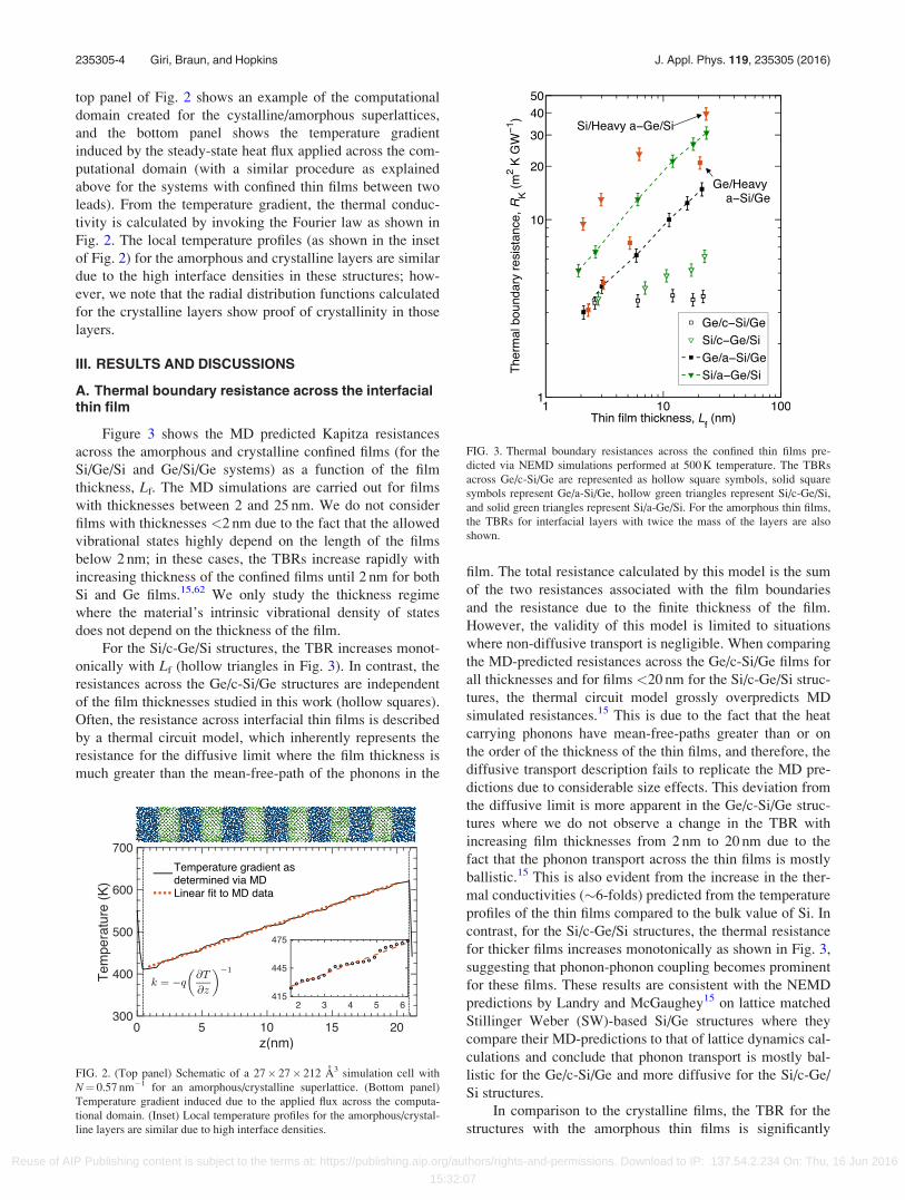
Figure 3 shows the MD predicted Kapitza resistances
across the amorphous and crystalline confined films (for the
Si/Ge/Si and Ge/Si/Ge systems) as a function of the film
thickness, Lf. The MD simulations are carried out for films
with thicknesses between 2 and 25 nm. We do not consider
films with thicknesses <2 nm due to the fact that the allowed
vibrational states highly depend on the length of the films
below 2 nm; in these cases, the TBRs increase rapidly with
increasing thickness of the confined films until 2 nm for both
Si and Ge films.15,62 We only study the thickness regime
where the material’s intrinsic vibrational density of states
does not depend on the thickness of the film.
For the Si/c-Ge/Si structures, the TBR increases monot-
onically with Lf (hollow triangles in Fig. 3). In contrast, the
resistances across the Ge/c-Si/Ge structures are independent
of the film thicknesses studied in this work (hollow squares).
Often, the resistance across interfacial thin films is described
by a thermal circuit model, which inherently represents the
resistance for the diffusive limit where the film thickness is
much greater than the mean-free-path of the phonons in the
film. The total resistance calculated by this model is the sum
of the two resistances associated with the film boundaries
and the resistance due to the finite thickness of the film.
However, the validity of this model is limited to situations
where non-diffusive transport is negligible. When comparing
the MD-predicted resistances across the Ge/c-Si/Ge films for
all thicknesses and for films <20 nm for the Si/c-Ge/Si struc-
tures, the thermal circuit model grossly overpredicts MD
simulated resistances.15 This is due to the fact that the heat
carrying phonons have mean-free-paths greater than or on
the order of the thickness of the thin films, and therefore, the
diffusive transport description fails to replicate the MD pre-
dictions due to considerable size effects. This deviation from
the diffusive limit is more apparent in the Ge/c-Si/Ge struc-
tures where we do not observe a change in the TBR with
increasing film thicknesses from 2 nm to 20 nm due to the
fact that the phonon transport across the thin films is mostly
ballistic.15 This is also evident from the increase in the ther-
mal conductivities (�6-folds) predicted from the temperature
profiles of the thin films compared to the bulk value of Si. In
contrast, for the Si/c-Ge/Si structures, the thermal resistance
for thicker films increases monotonically as shown in Fig. 3,
suggesting that phonon-phonon coupling becomes prominent
for these films. These results are consistent with the NEMD
predictions by Landry and McGaughey15 on lattice matched
Stillinger Weber (SW)-based Si/Ge structures where they
compare their MD-predictions to that of lattice dynamics cal-
culations and conclude that phonon transport is mostly bal-
listic for the Ge/c-Si/Ge and more diffusive for the Si/c-Ge/
Si structures.
In comparison to the crystalline films, the TBR for the
structures with the amorphous thin films is significantly
FIG. 2. (Top panel) Schematic of a 27� 27� 212 A3 simulation cell with
N¼ 0.57 nm�1 for an amorphous/crystalline superlattice. (Bottom panel)
Temperature gradient induced due to the applied flux across the computa-
tional domain. (Inset) Local temperature profiles for the amorphous/crystal-
line layers are similar due to high interface densities.
FIG. 3. Thermal boundary resistances across the confined thin films pre-
dicted via NEMD simulations performed at 500 K temperature. The TBRs
across Ge/c-Si/Ge are represented as hollow square symbols, solid square
symbols represent Ge/a-Si/Ge, hollow green triangles represent Si/c-Ge/Si,
and solid green triangles represent Si/a-Ge/Si. For the amorphous thin films,
the TBRs for interfacial layers with twice the mass of the layers are also
shown.
235305-4 Giri, Braun, and Hopkins J. Appl. Phys. 119, 235305 (2016)
Reuse of AIP Publishing content is subject to the terms at: https://publishing.aip.org/authors/rights-and-permissions. Download to IP: 137.54.2.234 On: Thu, 16 Jun 2016
15:32:07
greater for thicker films as shown in Fig. 3. The linear
increase in resistance is suggestive of diffusive transport
across the amorphous interfacial regions. Moreover, the
thickness trend in resistances predicted from the thermal
circuit model, which only considers the resistance due to
the amorphous layer (Lf/k), agrees well with the MD predic-
tions due to diffusive nature of heat propagation in the amor-
phous interfacial regions. Owing to the very low thermal
conductivities of the amorphous layers, it is very difficult to
accurately determine the resistance across a single amor-
phous/crystalline interface from the MD predicted tempera-
ture profiles for these structures. Typically, for crystalline
systems, the distinction between an interfacial resistance and
film thermal conductivity is well defined under the NEMD
framework due to the distinct temperature discontinuity at
interfaces. This distinction across the crystalline/amorphous
interfaces in our simulations is not clear, as the temperature
discontinuities at these interfaces are minute. However, the
accurate prediction of interfacial resistance at these bounda-
ries could be achieved via equilibrium MD simulations
where the resistance is calculated based on tracking the equi-
librium fluctuations and not dependent on the temperature dis-
continuity.63,64 Previously, this method has been used to
predict thermal interface conductance in crystalline/crystalline
Si/Ge superlattices63 and the resistance across a Lennard-Jones
based solid-gas interface.65 In fact, in Ref. 64, it is shown that
conductances calculated based on the equilibrium MD
approach are consistent with transmission describing diffusive
scattering, while the NEMD framework consistently describes
specular phonon scattering processes as determined for interfa-
ces consisting of atomically perfect Lennard-Jones solids.
Even though we cannot quantitatively prescribe an
accurate finite interface resistance, the NEMD-predicted
temperature profiles across our crystalline and amorphous
films suggest that the resistance across a single crystalline/
crystalline interface is greater than that at a single cystal-
line/amorphous interface. This result is consistent with
recent findings of interfacial resistance being higher across
a graphene/crystalline-SiC interface compared to a gra-
phene/amorphous-SiC interface, which was mainly attrib-
uted to a better overlap of density of states between the
graphene and amorphous-SiC compared to crystalline-
SiC.66 The lower resistance associated with amorphous sys-
tems is also similar to the findings reported in our previous
work on amorphous SLs where we show that the Kapitza
resistance across a single a-Si/a-Ge interface is �6 times
lower than between the corresponding crystalline materi-
als.67 Furthermore, Beechem and Hopkins68 have shown
that interfacial resistances predicted under the diffuse mis-
match model approach demonstrate lower resistances for an
amorphous/crystalline interface as compared to the predic-
tions for the crystalline counterparts. They attribute the
lower resistance at amorphous/crystalline interface to the
lack of abruptness of the system’s change from one material
to another, which ultimately augments heat flow across the
disordered interface. These results allude to the fact that
nanoscale imperfections around an interface could result in
higher energy transmission across the interface.
For the Si/a-Ge/Si structures, the values of TBR do not
agree with those of the Si/c-Ge/Si for all film thicknesses
considered. This can be mainly attributed to the lower ther-
mal conductivities of the amorphous Ge compared to its
crystalline counterpart. Increasing the mass of the “Ge” layer
by a factor of two also increases the TBR across the thin
films (red triangles in Fig. 3). In contrast, for the Ge/Si/Ge
structures with amorphous and crystalline films, the TBRs
for the thinner films (with Lf< 5 nm) are comparable in val-
ues with each other, regardless of the order and mass of the
interfacial region. Although the bandwidths in the density of
states for amorphous and crystalline Si are very similar to
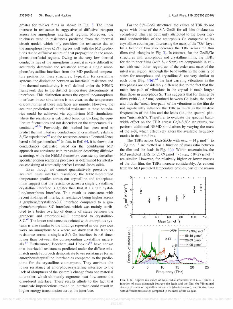
each other (Fig. 4(b)),67 the heat carrying vibrations in the
two phases are considerably different due to the fact that the
mean-free-path of vibrations in the crystal is much longer
than those in amorphous Si. This suggests that for thinner Si
films (with Lf< 5 nm) confined between Ge leads, the order
and thus the “mean-free-path” of the vibrations in the film do
not significantly influence the TBR as much as the relative
frequencies of the film and the leads (i.e., the spectral pho-
non “mismatch”). Therefore, to evaluate the spectral band-
width effect on the TBR across Ge/a-Si/Ge structures, we
perform additional NEMD simulations by varying the mass
of the a-Si, which effectively alters the available frequency
modes in the thin films.
The TBRs across Ge/a-Si/Ge with mfilm¼ 14 g mol�1 to
112 g mol�1 are plotted as a function of mass ratio between
the film and the leads in Fig. 4(a). Within uncertainties, the
MD predicted TBRs for 28.09 g mol�1<mfilm< 84.27 g mol�1
are similar. However, for relatively higher or lower masses
of the thin film, the TBRs increase considerably. As evident
from the MD predicted temperature profiles, part of the reason
FIG. 4. (a) Kapitza resistance of Ge/a-Si/Ge structures with Lf¼ 3 nm as a
function of mass-mismatch between the leads and the film. (b) Vibrational
density of states of crystalline Si and Ge (shaded region), and Si structures
with different mass ratios compared to the mass of the Ge lead.
235305-5 Giri, Braun, and Hopkins J. Appl. Phys. 119, 235305 (2016)
Reuse of AIP Publishing content is subject to the terms at: https://publishing.aip.org/authors/rights-and-permissions. Download to IP: 137.54.2.234 On: Thu, 16 Jun 2016
15:32:07
for the increase in TBRs for the heavier masses is due to the
reduction in thermal conductivities with increasing mass
(mfilm), while part of it is also due to the mismatch in the over-
lap of density of states between the film and the leads (calcu-
lated from the method described in Ref. 69) as shown in Fig.
4(b). The cutoff frequencies for the vibrational spectra shown
in Fig. 4(b) decrease with increasing mass due to the relation,
x / 1=ffiffiffiffiffiffiffiffiffiffi
mfilmp
. The vibrational spectra for 28.09 g mol�1
<mfilm < 84.27 g mol�1 fall within the cutoff frequency of
the crystalline Ge leads. Therefore, we do not observe a sig-
nificant difference in the TBR across films within this mass
range. However, for the film with relatively lighter mass
(mfilm¼ 14 g mol�1), even though the thermal conductivity
increases due to reduced mass, the drastic mismatch in the
overlap of density of states with that of the Ge leads (as shown
in Fig. 4(b)) significantly increases the TBR across the Ge/
light-a-Si/Ge structure. This suggests that the Kapitza resist-
ance across an individual amorphous/crystalline interface can
be increased by significantly enhancing the mismatch between
the density of the states of the two materials by effectively
creating a high mass ratio between the materials. This could
be particularly beneficial in designing SLs with small period
thicknesses (and high interface densities) where low thermal
conductivities are desired.
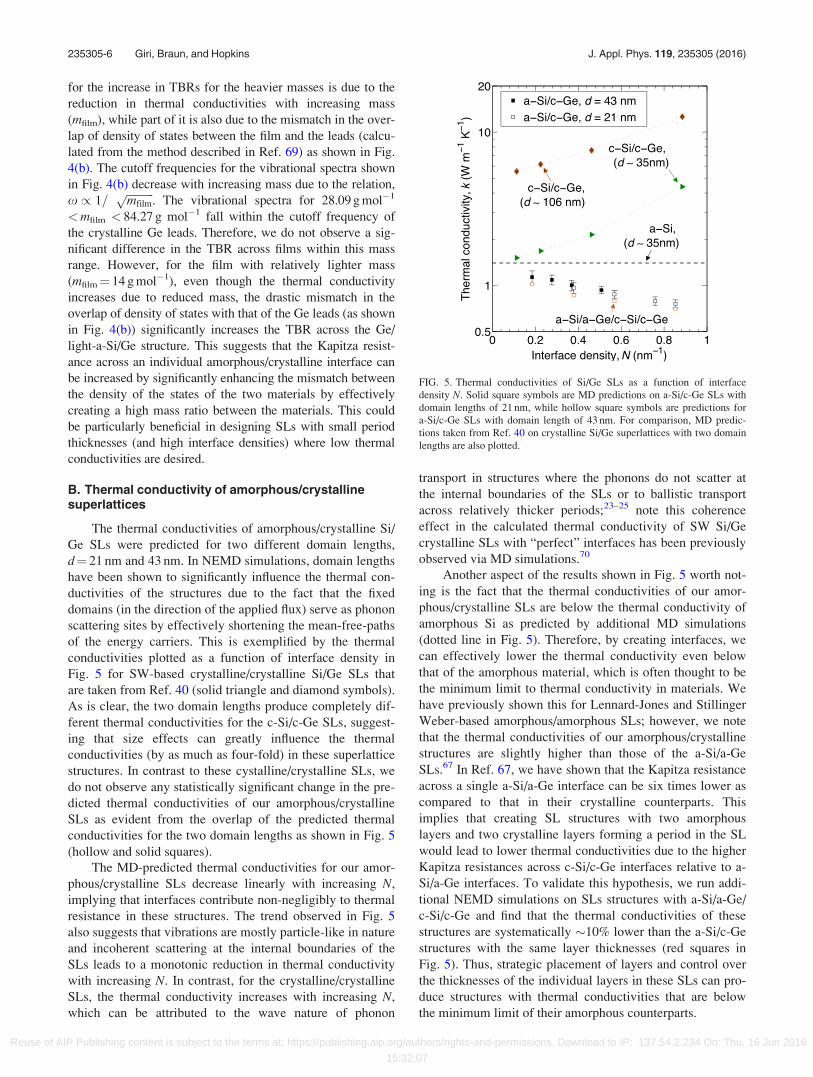
B. Thermal conductivity of amorphous/crystallinesuperlattices
The thermal conductivities of amorphous/crystalline Si/
Ge SLs were predicted for two different domain lengths,
d¼ 21 nm and 43 nm. In NEMD simulations, domain lengths
have been shown to significantly influence the thermal con-
ductivities of the structures due to the fact that the fixed
domains (in the direction of the applied flux) serve as phonon
scattering sites by effectively shortening the mean-free-paths
of the energy carriers. This is exemplified by the thermal
conductivities plotted as a function of interface density in
Fig. 5 for SW-based crystalline/crystalline Si/Ge SLs that
are taken from Ref. 40 (solid triangle and diamond symbols).
As is clear, the two domain lengths produce completely dif-
ferent thermal conductivities for the c-Si/c-Ge SLs, suggest-
ing that size effects can greatly influence the thermal
conductivities (by as much as four-fold) in these superlattice
structures. In contrast to these cystalline/crystalline SLs, we
do not observe any statistically significant change in the pre-
dicted thermal conductivities of our amorphous/crystalline
SLs as evident from the overlap of the predicted thermal
conductivities for the two domain lengths as shown in Fig. 5
(hollow and solid squares).
The MD-predicted thermal conductivities for our amor-
phous/crystalline SLs decrease linearly with increasing N,
implying that interfaces contribute non-negligibly to thermal
resistance in these structures. The trend observed in Fig. 5
also suggests that vibrations are mostly particle-like in nature
and incoherent scattering at the internal boundaries of the
SLs leads to a monotonic reduction in thermal conductivity
with increasing N. In contrast, for the crystalline/crystalline
SLs, the thermal conductivity increases with increasing N,
which can be attributed to the wave nature of phonon
transport in structures where the phonons do not scatter at
the internal boundaries of the SLs or to ballistic transport
across relatively thicker periods;23–25 note this coherence
effect in the calculated thermal conductivity of SW Si/Ge
crystalline SLs with “perfect” interfaces has been previously
observed via MD simulations.70
Another aspect of the results shown in Fig. 5 worth not-
ing is the fact that the thermal conductivities of our amor-
phous/crystalline SLs are below the thermal conductivity of
amorphous Si as predicted by additional MD simulations
(dotted line in Fig. 5). Therefore, by creating interfaces, we
can effectively lower the thermal conductivity even below
that of the amorphous material, which is often thought to be
the minimum limit to thermal conductivity in materials. We
have previously shown this for Lennard-Jones and Stillinger
Weber-based amorphous/amorphous SLs; however, we note
that the thermal conductivities of our amorphous/crystalline
structures are slightly higher than those of the a-Si/a-Ge
SLs.67 In Ref. 67, we have shown that the Kapitza resistance
across a single a-Si/a-Ge interface can be six times lower as
compared to that in their crystalline counterparts. This
implies that creating SL structures with two amorphous
layers and two crystalline layers forming a period in the SL
would lead to lower thermal conductivities due to the higher
Kapitza resistances across c-Si/c-Ge interfaces relative to a-
Si/a-Ge interfaces. To validate this hypothesis, we run addi-
tional NEMD simulations on SLs structures with a-Si/a-Ge/
c-Si/c-Ge and find that the thermal conductivities of these
structures are systematically �10% lower than the a-Si/c-Ge
structures with the same layer thicknesses (red squares in
Fig. 5). Thus, strategic placement of layers and control over
the thicknesses of the individual layers in these SLs can pro-
duce structures with thermal conductivities that are below
the minimum limit of their amorphous counterparts.
FIG. 5. Thermal conductivities of Si/Ge SLs as a function of interface
density N. Solid square symbols are MD predictions on a-Si/c-Ge SLs with
domain lengths of 21 nm, while hollow square symbols are predictions for
a-Si/c-Ge SLs with domain length of 43 nm. For comparison, MD predic-
tions taken from Ref. 40 on crystalline Si/Ge superlattices with two domain
lengths are also plotted.
235305-6 Giri, Braun, and Hopkins J. Appl. Phys. 119, 235305 (2016)
Reuse of AIP Publishing content is subject to the terms at: https://publishing.aip.org/authors/rights-and-permissions. Download to IP: 137.54.2.234 On: Thu, 16 Jun 2016
15:32:07
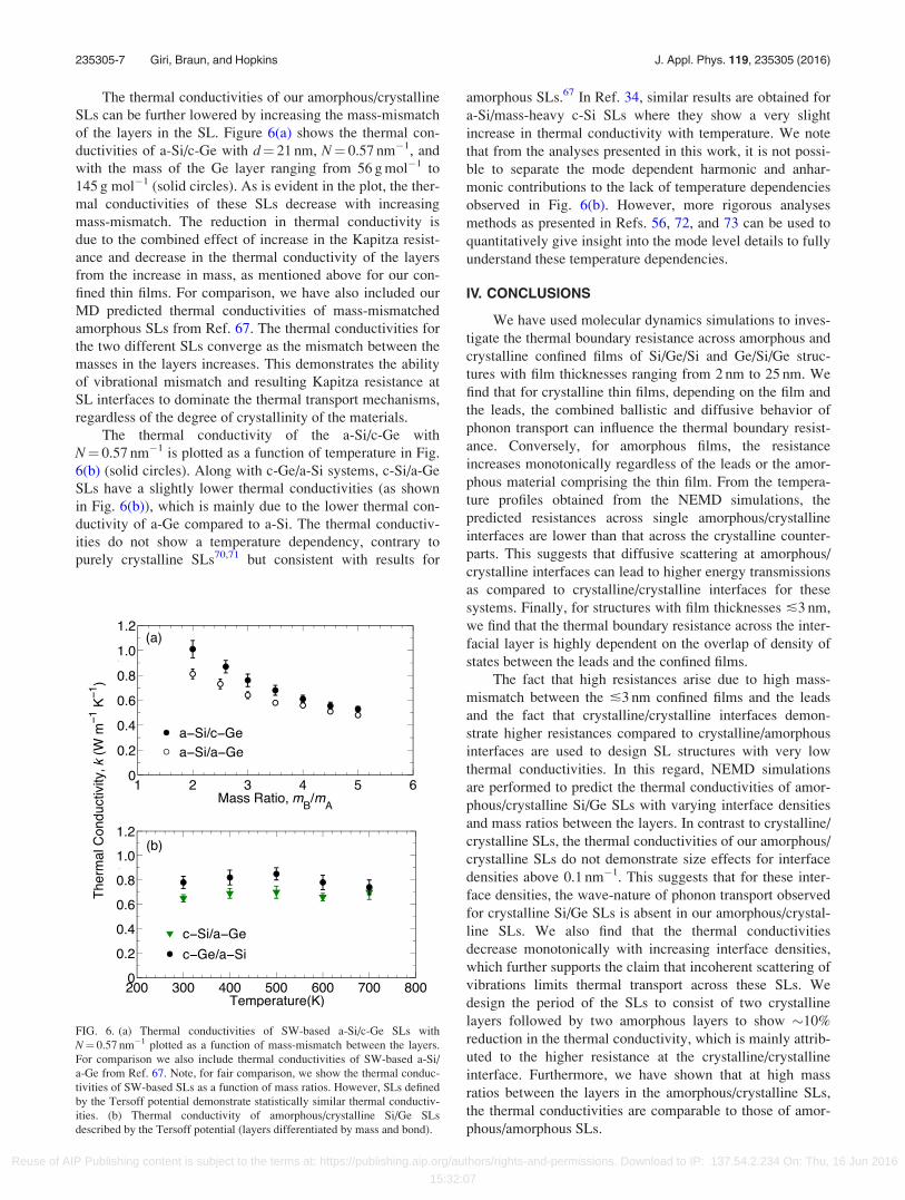
The thermal conductivities of our amorphous/crystalline
SLs can be further lowered by increasing the mass-mismatch
of the layers in the SL. Figure 6(a) shows the thermal con-
ductivities of a-Si/c-Ge with d¼ 21 nm, N¼ 0.57 nm�1, and
with the mass of the Ge layer ranging from 56 g mol�1 to
145 g mol�1 (solid circles). As is evident in the plot, the ther-
mal conductivities of these SLs decrease with increasing
mass-mismatch. The reduction in thermal conductivity is
due to the combined effect of increase in the Kapitza resist-
ance and decrease in the thermal conductivity of the layers
from the increase in mass, as mentioned above for our con-
fined thin films. For comparison, we have also included our
MD predicted thermal conductivities of mass-mismatched
amorphous SLs from Ref. 67. The thermal conductivities for
the two different SLs converge as the mismatch between the
masses in the layers increases. This demonstrates the ability
of vibrational mismatch and resulting Kapitza resistance at
SL interfaces to dominate the thermal transport mechanisms,
regardless of the degree of crystallinity of the materials.
The thermal conductivity of the a-Si/c-Ge with
N¼ 0.57 nm�1 is plotted as a function of temperature in Fig.
6(b) (solid circles). Along with c-Ge/a-Si systems, c-Si/a-Ge
SLs have a slightly lower thermal conductivities (as shown
in Fig. 6(b)), which is mainly due to the lower thermal con-
ductivity of a-Ge compared to a-Si. The thermal conductiv-
ities do not show a temperature dependency, contrary to
purely crystalline SLs70,71 but consistent with results for
amorphous SLs.67 In Ref. 34, similar results are obtained for
a-Si/mass-heavy c-Si SLs where they show a very slight
increase in thermal conductivity with temperature. We note
that from the analyses presented in this work, it is not possi-
ble to separate the mode dependent harmonic and anhar-
monic contributions to the lack of temperature dependencies
observed in Fig. 6(b). However, more rigorous analyses
methods as presented in Refs. 56, 72, and 73 can be used to
quantitatively give insight into the mode level details to fully
understand these temperature dependencies.
IV. CONCLUSIONS
We have used molecular dynamics simulations to inves-
tigate the thermal boundary resistance across amorphous and
crystalline confined films of Si/Ge/Si and Ge/Si/Ge struc-
tures with film thicknesses ranging from 2 nm to 25 nm. We
find that for crystalline thin films, depending on the film and
the leads, the combined ballistic and diffusive behavior of
phonon transport can influence the thermal boundary resist-
ance. Conversely, for amorphous films, the resistance
increases monotonically regardless of the leads or the amor-
phous material comprising the thin film. From the tempera-
ture profiles obtained from the NEMD simulations, the
predicted resistances across single amorphous/crystalline
interfaces are lower than that across the crystalline counter-
parts. This suggests that diffusive scattering at amorphous/
crystalline interfaces can lead to higher energy transmissions
as compared to crystalline/crystalline interfaces for these
systems. Finally, for structures with film thicknesses �3 nm,
we find that the thermal boundary resistance across the inter-
facial layer is highly dependent on the overlap of density of
states between the leads and the confined films.
The fact that high resistances arise due to high mass-
mismatch between the �3 nm confined films and the leads
and the fact that crystalline/crystalline interfaces demon-
strate higher resistances compared to crystalline/amorphous
interfaces are used to design SL structures with very low
thermal conductivities. In this regard, NEMD simulations
are performed to predict the thermal conductivities of amor-
phous/crystalline Si/Ge SLs with varying interface densities
and mass ratios between the layers. In contrast to crystalline/
crystalline SLs, the thermal conductivities of our amorphous/
crystalline SLs do not demonstrate size effects for interface
densities above 0.1 nm�1. This suggests that for these inter-
face densities, the wave-nature of phonon transport observed
for crystalline Si/Ge SLs is absent in our amorphous/crystal-
line SLs. We also find that the thermal conductivities
decrease monotonically with increasing interface densities,
which further supports the claim that incoherent scattering of
vibrations limits thermal transport across these SLs. We
design the period of the SLs to consist of two crystalline
layers followed by two amorphous layers to show �10%
reduction in the thermal conductivity, which is mainly attrib-
uted to the higher resistance at the crystalline/crystalline
interface. Furthermore, we have shown that at high mass
ratios between the layers in the amorphous/crystalline SLs,
the thermal conductivities are comparable to those of amor-
phous/amorphous SLs.
FIG. 6. (a) Thermal conductivities of SW-based a-Si/c-Ge SLs with
N¼ 0.57 nm�1 plotted as a function of mass-mismatch between the layers.
For comparison we also include thermal conductivities of SW-based a-Si/
a-Ge from Ref. 67. Note, for fair comparison, we show the thermal conduc-
tivities of SW-based SLs as a function of mass ratios. However, SLs defined
by the Tersoff potential demonstrate statistically similar thermal conductiv-
ities. (b) Thermal conductivity of amorphous/crystalline Si/Ge SLs
described by the Tersoff potential (layers differentiated by mass and bond).
235305-7 Giri, Braun, and Hopkins J. Appl. Phys. 119, 235305 (2016)
Reuse of AIP Publishing content is subject to the terms at: https://publishing.aip.org/authors/rights-and-permissions. Download to IP: 137.54.2.234 On: Thu, 16 Jun 2016
15:32:07
ACKNOWLEDGMENTS
We would like to thank the support from the Office of
Naval research (N00014-15-12769).
1E. T. Swartz and R. O. Pohl, Rev. Mod. Phys. 61, 605 (1989).2D. G. Cahill, W. K. Ford, K. E. Goodson, G. D. Mahan, A. Majumdar,
H. J. Maris, R. Merlin, and S. R. Phillpot, J. Appl. Phys. 93, 793 (2003).3D. G. Cahill, P. V. Braun, G. Chen, D. R. Clarke, S. Fan, K. E. Goodson,
P. Keblinski, W. P. King, G. D. Mahan, A. Majumdar, H. J. Maris, S. R.
Phillpot, E. Pop, and L. Shi, Appl. Phys. Rev. 1, 011305 (2014).4E. Pop, Nano Res. 3, 147 (2010).5Y.-L. Li, Y.-R. Huang, and Y.-H. Lai, Appl. Phys. Lett. 91, 181113
(2007).6G. Chen, M. S. Dresselhaus, G. Dresselhaus, J.-P. Fleurial, and T. Caillat,
Int. Mater. Rev. 48, 45 (2003).7M. Dresselhaus, G. Chen, M. Tang, R. Yang, H. Lee, D. Wang, Z. Ren,
J.-P. Fleurial, and P. Gogna, Adv. Mater. 19, 1043 (2007).8P. E. Hopkins, ISRN Mech. Eng. 2013, 682586.9R. M. Costescu, M. A. Wall, and D. G. Cahill, Phys. Rev. B 67, 054302
(2003).10B. Krenzer, A. Hanisch-Blicharski, P. Schneider, T. Payer, S. M€ollenbeck,
O. Osmani, M. Kammler, R. Meyer, and M. Horn-von Hoegen, Phys. Rev.
B 80, 024307 (2009).11A. Hanisch, B. Krenzer, T. Pelka, S. M€ollenbeck, and M. Horn-von
Hoegen, Phys. Rev. B 77, 125410 (2008).12J. Wang and J.-S. Wang, J. Phys.: Condens. Matter 19, 236211 (2007).13F. Jolly, F. Rochet, G. Dufour, C. Grupp, and A. Taleb-Ibrahimi, J. Non-
Cryst. Solids 280, 150 (2001).14T. S. English, J. C. Duda, J. L. Smoyer, D. A. Jordan, P. M. Norris, and L.
V. Zhigilei, Phys. Rev. B 85, 035438 (2012).15E. S. Landry and A. J. H. McGaughey, J. Appl. Phys. 107, 013521 (2010).16E. S. Landry and A. J. H. McGaughey, Phys. Rev. B 80, 165304 (2009).17D. G. Cahill, S. K. Watson, and R. O. Pohl, Phys. Rev. B 46, 6131 (1992).18H. Mizuno, S. Mossa, and J.-L. Barrat, Sci. Rep. 5, 14116 EP (2015).19E. Dechaumphai, D. Lu, J. J. Kan, J. Moon, E. E. Fullerton, Z. Liu, and R.
Chen, Nano Lett. 14, 2448 (2014).20X. Mu, X. Wu, T. Zhang, D. B. Go, and T. Luo, Sci. Rep. 4, 3909 EP
(2014).21C. Chiritescu, D. G. Cahill, N. Nguyen, D. Johnson, A. Bodapati, P.
Keblinski, and P. Zschack, Science 315, 351 (2007).22G. Pernot, M. Stoffel, I. Savic, F. Pezzoli, P. Chen, G. Savelli, A. Jacquot,
J. Schumann, U. Denker, I. M€onch, C. Deneke, O. G. Schmidt, J. M.
Rampnoux, S. Wang, M. Plissonnier, A. Rastelli, S. Dilhaire, and N.
Mingo, Nat. Mater. 9, 491 (2010).23M. V. Simkin and G. D. Mahan, Phys. Rev. Lett. 84, 927 (2000).24M. N. Luckyanova, J. Garg, K. Esfarjani, A. Jandl, M. T. Bulsara, A. J.
Schmidt, A. J. Minnich, S. Chen, M. S. Dresselhaus, Z. Ren, E. A.
Fitzgerald, and G. Chen, Science 338, 936 (2012).25J. Ravichandran, A. K. Yadav, R. Cheaito, P. B. Rossen, A. Soukiassian,
S. J. Suresha, J. C. Duda, B. M. Foley, C.-H. Lee, Y. Zhu, A. W.
Lichtenberger, J. E. Moore, D. A. Muller, D. G. Schlom, P. E. Hopkins, A.
Majumdar, R. Ramesh, and M. A. Zurbuchen, Nat. Mater. 13, 168 (2014).26Y. Wang, H. Huang, and X. Ruan, Phys. Rev. B 90, 165406 (2014).27Y. Chen, D. Li, J. R. Lukes, Z. Ni, and M. Chen, Phys. Rev. B 72, 174302
(2005).28G. Chen, J. Heat Transfer 119, 220 (1997).29E. S. Landry, M. I. Hussein, and A. J. H. McGaughey, Phys. Rev. B 77,
184302 (2008).30Z. Aksamija and I. Knezevic, Phys. Rev. B 88, 155318 (2013).31M. Hu and D. Poulikakos, Nano Lett. 12, 5487 (2012).32S. T. Huxtable, A. R. Abramson, C.-L. Tien, A. Majumdar, C. LaBounty,
X. Fan, G. Zeng, J. E. Bowers, A. Shakouri, and E. T. Croke, Appl. Phys.
Lett. 80, 1737 (2002).
33D. Li, Y. Wu, R. Fan, P. Yang, and A. Majumdar, Appl. Phys. Lett. 83,
3186 (2003).34A. France-Lanord, S. Merabia, T. Albaret, D. Lacroix, and K.
Termentzidis, J. Phys.: Condens. Matter 26, 355801 (2014).35Z. Zhang, J. Roger, D. Fournier, A. Boccara, and J. Wang, Thin Solid
Films 186, 361 (1990).36B. Shen, Z. Zeng, C. Lin, and Z. Hu, Int. J. Therm. Sci. 66, 19 (2013).37A. Descoeudres, L. Barraud, S. De Wolf, B. Strahm, D. Lachenal, C.
Gucrin, Z. C. Holman, F. Zicarelli, B. Demaurex, J. Seif, J. Holovsky, and
C. Ballif, Appl. Phys. Lett. 99, 123506 (2011).38H. Ohta, R. Huang, and Y. Ikuhara, Phys. Status Solidi RRL 2, 105
(2008).39R. W. Fathauer, T. George, E. W. Jones, W. T. Pike, A. Ksendzov, and R.
P. Vasquez, Appl. Phys. Lett. 61, 2350 (1992).40K.-H. Lin and A. Strachan, Phys. Rev. B 87, 115302 (2013).41S. Plimpton, J. Comput. Phys. 117, 1 (1995).42J. Tersoff, Phys. Rev. B 37, 6991 (1988).43J. Tersoff, Phys. Rev. B 39, 5566 (1989).44W. G. Hoover, Phys. Rev. A 31, 1695 (1985).45Z. Liang and P. Keblinski, Phys. Rev. B 90, 075411 (2014).46S. Majumdar, J. A. Sierra-Suarez, S. N. Schiffres, W.-L. Ong, I. C. Fred
Higgs, A. J. H. McGaughey, and J. A. Malen, Nano Lett. 15, 2985
(2015).47H. Acharya, N. J. Mozdzierz, P. Keblinski, and S. Garde, Ind. Eng. Chem.
Res. 51, 1767 (2012).48B. H. Kim, A. Beskok, and T. Cagin, J. Chem. Phys. 129, 174701
(2008).49Z. Liang, W. Evans, and P. Keblinski, Phys. Rev. E 87, 022119 (2013).50Z. Liang, W. Evans, T. Desai, and P. Keblinski, Appl. Phys. Lett. 102,
061907 (2013).51Z. Liang and P. Keblinski, Int. J. Heat Mass Transfer 78, 161 (2014).52K. Gordiz and A. Henry, New J. Phys. 17, 103002 (2015).53K. Gordiz and A. Henry, Sci. Rep. 6, 23139 EP (2016).54Y. Chalopin, N. Mingo, J. Diao, D. Srivastava, and S. Volz, Appl. Phys.
Lett. 101, 221903 (2012).55Y. Chalopin and S. Volz, Appl. Phys. Lett. 103, 051602 (2013).56K. S€a€askilahti, J. Oksanen, J. Tulkki, and S. Volz, Phys. Rev. B 90,
134312 (2014).57T. Murakami, T. Hori, T. Shiga, and J. Shiomi, Appl. Phys. Express 7,
121801 (2014).58A. France-Lanord, E. Blandre, T. Albaret, S. Merabia, D. Lacroix, and K.
Termentzidis, J. Phys.: Condens. Matter 26, 055011 (2014).59W. Shinoda, M. Shiga, and M. Mikami, Phys. Rev. B 69, 134103
(2004).60D. Hondongwa, L. Olasov, B. Daly, S. King, and J. Bielefeld, Thin Solid
Films 519, 7895 (2011).61S.-M. Lee, D. G. Cahill, and T. H. Allen, Phys. Rev. B 52, 253 (1995).62C. Shao and H. Bao, Int. J. Heat Mass Transfer 85, 33 (2015).63Y. Chalopin, K. Esfarjani, A. Henry, S. Volz, and G. Chen, Phys. Rev. B
85, 195302 (2012).64S. Merabia and K. Termentzidis, Phys. Rev. B 86, 094303 (2012).65B. Peng, W. He, X. Hao, Y. Chen, and Y. Liu, Comput. Mater. Sci. 87,
260 (2014).66M. Li, J. Zhang, X. Hu, and Y. Yue, Appl. Phys. A 119, 415 (2015).67A. Giri, P. E. Hopkins, J. G. Wessel, and J. C. Duda, J. Appl. Phys. 118,
165303 (2015).68T. Beechem and P. E. Hopkins, J. Appl. Phys. 106, 124301 (2009).69J. C. Duda, T. S. English, E. S. Piekos, W. A. Soffa, L. V. Zhigilei, and P.
E. Hopkins, Phys. Rev. B 84, 193301 (2011).70E. S. Landry and A. J. H. McGaughey, Phys. Rev. B 79, 075316 (2009).71Y. K. Koh, Y. Cao, D. G. Cahill, and D. Jena, Adv. Funct. Mater. 19, 610
(2009).72W. Lv and A. Henry, New J. Phys. 18, 013028 (2016).73M. Gill-Comeau and L. J. Lewis, Phys. Rev. B 92, 195404 (2015).
235305-8 Giri, Braun, and Hopkins J. Appl. Phys. 119, 235305 (2016)
Reuse of AIP Publishing content is subject to the terms at: https://publishing.aip.org/authors/rights-and-permissions. Download to IP: 137.54.2.234 On: Thu, 16 Jun 2016
15:32:07