Embed Size (px)
Citation preview

九州大学大学院システム情報科学府
電気電子工学専攻
平成29年度入学試験問題
【平成28年8月18日(木)、19日(金)】

平成29年度 九州大学大学院システム情報科学府情報学専攻情報知能工学専攻電気電子工学専攻
修士課程 入学試験問題
数 学 (Mathematics)(7枚中の 1)
解答上の注意 (Instructions):
1. 問題用紙は,『始め』の合図があるまで開いてはならない.
Do not open this cover sheet until the start of examination is announced.
2. 問題用紙は表紙を含め 7枚,解答用紙は 3枚つづり (1分野につき 1枚)である.
You are given 7 problem sheets including this cover sheet, and 3 answer sheets (1 sheet for
each field).
3. 以下の 6分野から 3分野を選び解答すること.選んだ分野毎に解答用紙を別にすること.
Select 3 fields out of the following 6 fields and answer the questions. You must use a separate
answer sheet for each of the fields you selected.
分野 field page
1 線形代数 Linear algebra 2
2 微分方程式 Differential equation 3
3 ベクトル解析 Vector analysis 4
4 複素関数論 Complex function theory 5
5 確率・統計 Probability and statistics 6
6 記号論理学 Symbolic logic 7
4. 解答用紙の全部に,専攻名,コース名(情報学専攻を除く),選択分野番号(で囲む),受
験番号および氏名を記入すること.
Fill in the designated blanks at the top of each answer sheet with the department name,
course name (except the department of informatics), the selected field number (mark with a
circle), your examinee number and your name.
5. 解答は解答用紙に記入すること.スペースが足りない場合は裏面を用いても良いが,その場
合は,裏面に解答があることを明記すること.
Write your answers on the answer sheets. You may use the backs of the answer sheets when
you run out of space. If you do so, indicate it clearly on the sheet.

平成29年度 九州大学大学院システム情報科学府情報学専攻情報知能工学専攻電気電子工学専攻
修士課程 入学試験問題
数 学 (Mathematics)(7枚中の 2)
6分野のうちから 3分野を選び解答すること.選んだ分野毎に解答用紙を別にすること.Select 3 fields out of the 6 fields and answer the questions. Use a separate answer sheetfor each field.
1. 【線形代数 (Linear algebra)分野】
1次独立なn次元ベクトルの組v1,v2, . . . ,vk ⊆ Rn が張る部分空間Kに対し,写像 f : K →
Rkを次のように定義する.任意の x =∑k
i=1 αivi ∈ Kに対し,f(x) =
α1
...
αk
.以下の各問に答えよ.
(1) 任意の x,y ∈ Kに対し,f(x+ y) = f(x) + f(y)が成り立つことを示せ.
(2) 任意の x ∈ K,任意の実数 cに対し,f(cx) = cf(x)が成り立つことを示せ.
(3) x1,x2, . . . ,xl ⊆ Kが 1次独立のとき,f(x1), f(x2), . . . , f(xl)も 1次独立であるこ
とを示せ.
For a subspaceK spanned by a linearly independent set of n dimensional vectors v1,v2, . . . ,vk ⊆
Rn, we define a function f : K → Rk as f(x) =
α1
...
αk
for any x =∑k
i=1 αivi ∈ K.
Answer the following questions.
(1) Show that f(x+ y) = f(x) + f(y) for any x,y ∈ K.
(2) Show that f(cx) = cf(x) for any x ∈ K and any real number c.
(3) Show that if x1,x2, . . . ,xl ⊆ K is linearly independent, then so is f(x1), f(x2), . . . , f(xl).

平成29年度 九州大学大学院システム情報科学府情報学専攻情報知能工学専攻電気電子工学専攻
修士課程 入学試験問題
数 学 (Mathematics)(7枚中の 3)
6分野のうちから 3分野を選び解答すること.選んだ分野毎に解答用紙を別にすること.Select 3 fields out of the 6 fields and answer the questions. Use a separate answer sheetfor each field.
2. 【微分方程式 (Differential equation)分野】
次の微分方程式の一般解を求めよ.
(1)dy
dx+y
x=
1
1 + x2
(2) (√xy − x)
dy
dx= −y
Find general solutions to the following differential equations.
(1)dy
dx+y
x=
1
1 + x2
(2) (√xy − x)
dy
dx= −y

平成29年度 九州大学大学院システム情報科学府情報学専攻情報知能工学専攻電気電子工学専攻
修士課程 入学試験問題
数 学 (Mathematics)(7枚中の 4)
6分野のうちから 3分野を選び解答すること.選んだ分野毎に解答用紙を別にすること.Select 3 fields out of the 6 fields and answer the questions. Use a separate answer sheetfor each field.
3. 【ベクトル解析 (Vector analysis)分野】
次の各問に答えよ.ただし (x, y, z)は三次元空間の直交座標を表す.
(1) スカラー場 ϕ = x2yz3 + xy2zについて,点 (1,3,2)における∇ · (∇ϕ)を計算せよ.
(2) スカラー場 V = xyz について,次の面 Sに対する V の面積分を計算せよ.
S : x2 + y2 = 4, x ≥ 0, y ≥ 0, 3 ≥ z ≥ 0
Answer the following questions, where (x, y, z) denotes Cartesian coordinates.
(1) For the scalar field ϕ = x2yz3 + xy2z, determine ∇ · (∇ϕ) at the point (1,3,2).
(2) Evaluate the surface integral for the scalar field V = xyz, over the following surface S.
S : x2 + y2 = 4, x ≥ 0, y ≥ 0, 3 ≥ z ≥ 0.

平成29年度 九州大学大学院システム情報科学府情報学専攻情報知能工学専攻電気電子工学専攻
修士課程 入学試験問題
数 学 (Mathematics)(7枚中の 5)
6分野のうちから 3分野を選び解答すること.選んだ分野毎に解答用紙を別にすること.Select 3 fields out of the 6 fields and answer the questions. Use a separate answer sheetfor each field.
4. 【複素関数論 (Complex function theory)分野】
複素関数w(z) =z − 1
z + 1を考える.ただし,z = x+ iy,i =
√−1,xと yは実数である.
次の各問に答えよ.
(1) w(z) = u(x, y) + iv(x, y)で表されるとき,u(x, y)と v(x, y)を求めよ.
ただし,u(x, y)と v(x, y)は実数値関数である.
(2) 以下の領域Aの関数w(z)による像w(A) = w(z) | z ∈ Aを複素平面上に図示せよ.(a) A = z ∈ C |x = 0,(b) A = z ∈ C |x = 1,(c) A = z ∈ C | y = 0,x ≥ 0
Consider the complex function w(z) =z − 1
z + 1, where z = x + iy, i =
√−1, and x and y are
real numbers. Answer the following questions.
(1) Denote the function w(z) as w(z) = u(x, y) + iv(x, y), where the functions u(x, y) and
v(x, y) are real-valued. Then, find the functions u(x, y) and v(x, y).
(2) Illustrate in the complex plane the images w(A) = w(z) | z ∈ A of the following regionsA through the function w(z).
(a) A = z ∈ C |x = 0, (b) A = z ∈ C |x = 1, (c) A = z ∈ C | y = 0,x ≥ 0.

平成29年度 九州大学大学院システム情報科学府情報学専攻情報知能工学専攻電気電子工学専攻
修士課程 入学試験問題
数 学 (Mathematics)(7枚中の 6)
6分野のうちから 3分野を選び解答すること.選んだ分野毎に解答用紙を別にすること.Select 3 fields out of the 6 fields and answer the questions. Use a separate answer sheetfor each field.
5. 【確率・統計 (Probability and statistics)分野】
離散確率変数X1, . . . , Xnは独立に,確率分布
Pr[Xi = k] =
(1
2
)k
(k = 1, 2, . . .)
に従うものとする.以下の各問に答えよ.
(1)∑n
i=1Xiの期待値を求めよ.
(2) Pr[Xi ≤ k] (k = 1, 2, . . .)を求めよ.
(3) Z = maxi∈1,...,nXiとする.Pr[Z ≤ k] (k = 1, 2, . . .)を求めよ.
(4) nが十分に大きいとき,Pr[Z ≤ log2 n− 1] ≥ 1/2が成り立つか否か,理由と共に述べよ.
ただし自然対数の底 eに対して,1/e < 0.37が成り立つことを用いてよい.
Let X1, . . . , Xn be independent discrete random variables with probability
Pr[Xi = k] =
(1
2
)k
(k = 1, 2, . . .).
Answer the following questions.
(1) Find the expectation of∑n
i=1Xi.
(2) Find Pr[Xi ≤ k] (k = 1, 2, . . .).
(3) Let Z = maxi∈1,...,nXi. Find Pr[Z ≤ k] (k = 1, 2, . . .).
(4) Establish whether or not Pr[Z ≤ log2 n − 1] ≥ 1/2 holds for sufficiently large n. You
can use the fact that 1/e < 0.37 for e, the base of the natural logarithm.

平成29年度 九州大学大学院システム情報科学府情報学専攻情報知能工学専攻電気電子工学専攻
修士課程 入学試験問題
数 学 (Mathematics)(7枚中の 7)
6分野のうちから 3分野を選び解答すること.選んだ分野毎に解答用紙を別にすること.Select 3 fields out of the 6 fields and answer the questions. Use a separate answer sheetfor each field.
6. 【記号論理学 (Symbolic logic)分野】
(1) (p → (q → (r ∧ s))) → (¬((¬s ∨ ¬r) → ¬q) → ¬p) がトートロジーであることをタブロー法により示せ.
(2) 赤や緑の電球がいくつかある.以下の問いに答えよ.
(a) 以下の文章ψ1, ψ2, ϕのそれぞれを論理式で表せ.ただし,「xは赤電球」をR(x),「x
は緑電球」をG(x),「xが点灯中」を L(x)で表せ.
ψ1: 点灯中でない緑電球があるならば,点灯中の赤電球がある.
ψ2: 点灯中の緑電球があるのは,点灯中でない赤電球があるとき,かつそのとき
に限る.
ϕ: 点灯中の赤電球があるならば,点灯中の緑電球はない
(b) 上の ϕはψ1とψ2からの論理的帰結か否かを答えよ.もし論理的帰結ならば,理由
を説明せよ.そうでないならば,反例を示せ.
(1) Prove by the tableaux method that (p→ (q → (r ∧ s)))→ (¬((¬s ∨ ¬r)→ ¬q)→ ¬p)is a tautology.
(2) There are some red bulbs and green bulbs. Answer the following questions.
(a) Express each of the following sentences ψ1, ψ2 and ϕ in a logical formula using the
predicates R(x), G(x), and L(x) which represent “x is a red bulb,” “x is a green
bulb,” and “x is on,” respectively.
ψ1: There exists a red bulb which is on if there exists a green bulb which is not
on.
ψ2: There exists a green bulb which is on if and only if there exists a red bulb
which is not on.
ϕ: There exists no green bulb which is on if there exists a red bulb which is on.
(b) Is ϕ a logical consequence of ψ1 and ψ2? If so explain the reason, otherwise give a
counter example.

平成 29年度 九州大学大学院システム情報科学府 電気電子工学専攻
修士課程 入学試験問題
専門Ⅰ (Special subjects I)
解答上の注意 (Instructions):
1. 問題用紙は,『始め』の合図があるまで開いてはならない.
Do not open this cover sheet until the start of examination is announced.
2. 問題用紙は表紙を含め 9枚,解答用紙は 3枚である.
You are given 9 problem sheets including this cover sheet, and 3 answer sheets.
3. 以下の 3分野から 1分野を選び解答すること.
Select 1 out of the following 3 fields and answer the questions.
分野 field page
1 電気回路 Circuit theory 2 ~
2 電子回路 Electronic circuits 4 ~
3 制御工学 Control engineering 6 ~
4. 解答は解答用紙に記入すること.大問一つあたり一枚の解答用紙を用いよ.スペース
が足りない場合は裏面を用いても良いが,その場合は,裏面に解答があることを明記
すること.
Your answers should be written on the answer sheets. Use one sheet for each
question. You may continue to write your answer on the back of the answer sheets if
you need more space. In such a case, indicate this clearly.
5. 解答用紙の全部に,志望するコース名,選択分野名,受験番号,氏名および問題番号
を記入すること.
Fill in the designated blanks at the top of each answer sheet with the course name,
your selected field name, your examinee number, your name and the question
number.
1

電気回路
4問中 3問を選び,解答用紙欄に解答した問題番号を記入すること.
【問 1】 図 1の回路において,電源電圧Eと電流 Iの位相
差は arg
(E
I
)= 0であり,かつX1 = X2 である.以下の
問いに答えよ.
(1) R, X1, X2の間の関係を示せ.
(2) |E| = 8 V, |I| = 2 A,|I1||I2|
= 2 のとき,R, X1, X2の
値を求めよ.
jX1E
I
-jX2
R R
I1 I2
図 1
【問 2】 図 2の回路について,以下の問いに答えよ.
(1)
(V1I1
)=
(a b
c d
)(V2I2
)のとき,Zと Y を用いて
行列
(a b
c d
)を表せ.
(2) 端子対 2-2’にインピーダンス ZK をつないだところ,端子対 1-1’から右側を見たインピーダンスもZK となった.Zと Y を用いてZK を表せ.
図 2
【問 3】 図 3の回路について,以下の問いに答えよ.ただし,電源の角周波数を ωとする.
(1) 節点電位 Va, Vb, Vcに対する回路方程式を立てよ.
(2) Vb = Vcのとき,R0 ~ R5, C3, C4, ωが満たすべき条件を求めよ.
R1
J
Va
VbVc
R5
R2
R3
R4
R0
C4
C3
図 3
【問 4】 図 4の回路において,時刻 t = 0でスイッチを S1
から S2に切り替えるとする.ただし,t < 0の回路は定常状態にあるとする.また,e1(t) = 4 sin 2t V,E2 = 8 V,R1 = 2 Ω,R2 = 4 Ω,L = 1 H,C = 0.125 Fとする.以下の問いに答えよ.
(1) スイッチを切り替える前の電荷 q(t)(t < 0)を求めよ.
(2) スイッチを切り替えた後の電荷 q(t)(t > 0)を求めよ.
q(t)
S1
R1
e1(t)
S2
L R2
E2C
図 4
2

Circuit Theory
Choose three out of the four questions and write the chosen question number on each answer sheet.
【Q1】 Consider the circuit shown in Fig. 1, where the
phase difference arg
(E
I
)= 0 and X1 = X2.
(1) Find the equation representing the relation among R,
X1 and X2.
(2) Find the values of R, X1 and X2, where |E| = 8 V,
|I| = 2 A and|I1||I2|
= 2.
jX1E
I
-jX2
R R
I1 I2
Fig. 1
【Q2】 Consider the circuit shown in Fig. 2.
(1) Find the matrix
(a b
c d
)for
(V1I1
)=
(a b
c d
)(V2I2
)using Z and Y .
(2) When the terminal pair 2-2’ is connected by an
impedance ZK , the impedance between the terminal
pair 1-1’ also becomes ZK . Find ZK using Z and Y .Fig. 2
【Q3】 Consider the circuit shown in Fig. 3, where the
source has the angular frequency ω. Answer the following
questions.
(1) Write the circuit equations using the node potentials
Va, Vb and Vc as variables.
(2) Derive the requirements to be satisfied by R0 to R5,
C3, C4 and ω if Vb = Vc.
R1
J
Va
VbVc
R5
R2
R3
R4
R0
C4
C3
Fig. 3
【Q4】 In Fig. 4, the switch is connected to S1, and the
circuit is in steady state. Then, the switch is changed from
S1 to S2 at the time t = 0. Answer the following questions
when e1(t) = 4 sin 2t V, E2 = 8 V, R1 = 2 Ω, R2 = 4 Ω,
L = 1 H and C = 0.125 F.
(1) Find the charge q(t) (t < 0) before changing the
switch.
(2) Find the charge q(t) (t > 0) after changing the
switch.
q(t)
S1
R1
e1(t)
S2
L R2
E2C
Fig. 4
3
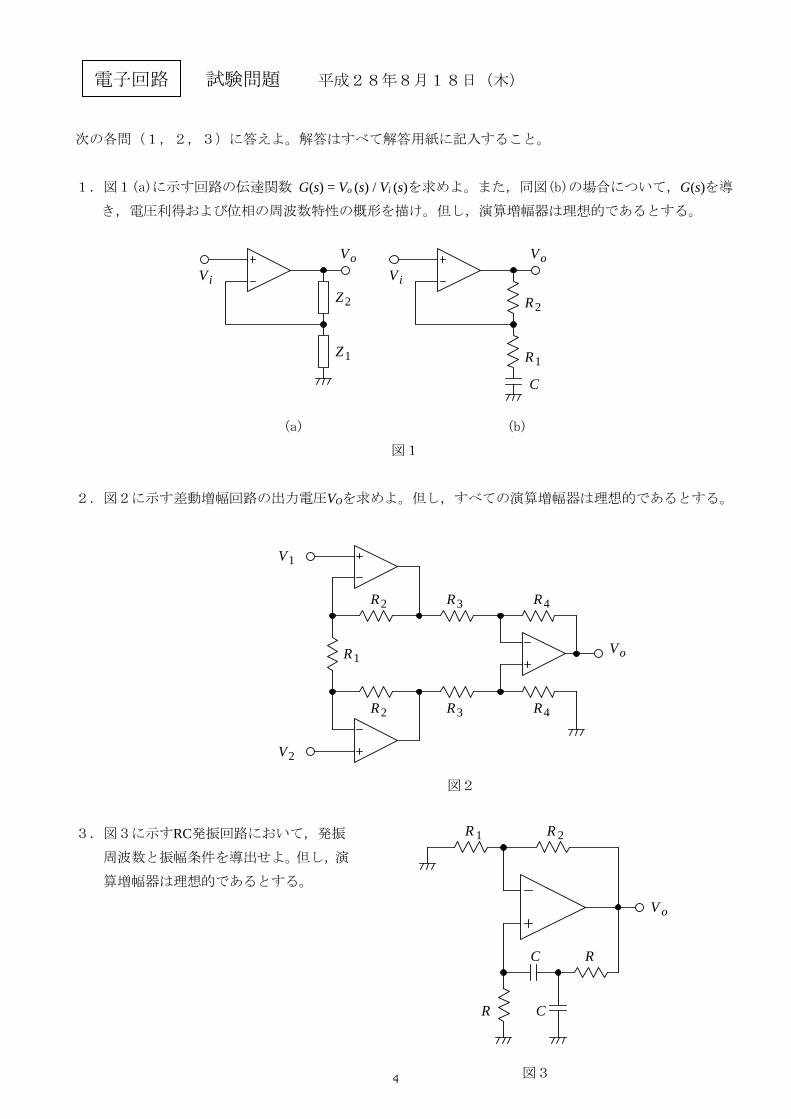
電子回路 試験問題 平成28年8月18日(木)
次の各問(1,2,3)に答えよ。解答はすべて解答用紙に記入すること。
1.図1(a)に示す回路の伝達関数 G(s) = Vo (s) / Vi (s)を求めよ。また,同図(b)の場合について,G(s)を導
き,電圧利得および位相の周波数特性の概形を描け。但し,演算増幅器は理想的であるとする。
(a) (b)
図1
2.図2に示す差動増幅回路の出力電圧VOを求めよ。但し,すべての演算増幅器は理想的であるとする。
1V
2V
2R
2R
1R
3R 4R
3R 4R
oV
図2
3.図3に示すRC発振回路において,発振
周波数と振幅条件を導出せよ。但し,演
算増幅器は理想的であるとする。
図3
V o
R 1 R 2
R
RC
C
1Z
iV
oV
2Z
iV
oV
1R
2R
C
4

ELECTRONIC CIRCUITS
Aug.18, 2016
Answer the following questions (1, 2, 3). All answers should be written on the answer sheets.
1. Derive the transfer function G(s) = Vo (s) / Vi (s) for the circuit shown in Fig. 1 (a). Then, derive G(s) for the
circuit shown in Fig. 1 (b), and sketch the frequency characteristics of the voltage gain and the phase. The
operational amplifiers are assumed to be ideal.
(a) (b)
Fig. 1
2. Derive the output voltage Vo of the differential amplifier circuit shown in Fig. 2. All operational amplifiers are
assumed to be ideal.
1V
2V
2R
2R
1R
3R 4R
3R 4R
oV
Fig. 2
3. Fig. 3 shows an RC oscillator circuit, where the
operational amplifier is assumed to be ideal.
Derive the oscillation frequency and the condition
for the amplitude of the loop gain.
Fig. 3
V o
R 1 R 2
R
RC
C
1Z
iV
oV
2Z
iV
oV
1R
2R
C
5

制御工学
次の各問([1],[2],[3])に答えよ.
[1]
次のように表されるシステムを考える.
x(t) =
[a 00 b
]x(t) +
[c
d
]u(t),
y(t) =[
e f]x(t)
ここで,a,b,c,d,e,f は実数,xは状態ベクトル,yは出力ベクトル,uは入力ベクトルである.
1. uと yの次元を答えよ.
2. このシステムの双対システムを示せ.
3. この双対システムが可制御となるための必要十分条件を示せ.
4. この双対システムの伝達関数と,もとのシステムの伝達関数とは一致することを示せ.
[2]
下に示すブロック図で表されるフィードバック系について考える.
( )k s
s
( )
( )
b s
a s+
++
−
r e
d
yu
ここで rは参照信号,dは外乱.k(s),a(s),b(s) は実係数の sの多項式,sはラプラス演算子. k(0) = 0かつ b(0) = 0である.
1. r(s) = 1/s, d(s) = e−s/sとする.eが 0に収束する条件を語句 “複素平面”を用いて説明せよ.
2. 前問の条件下で,eの収束に対応した uの極限値を計算せよ.
6

[3]
下に示すブロック線図で表されるシステムを考える.このシステムの入力は u(t),出力は y(t)である.図ではすべての信号をそのラプラス変換で表示している.ただし,信号 f(t)のラプラス変換は F (s)で表すものとする.
1. このシステムの状態変数ベクトルを適切に定義し,このシステムを表す状態方程式と出力方程式を導け.ただし,状態変数ベクトルの次元は最小のものとする.
2. このシステムの BIBO安定性を判別せよ.
7
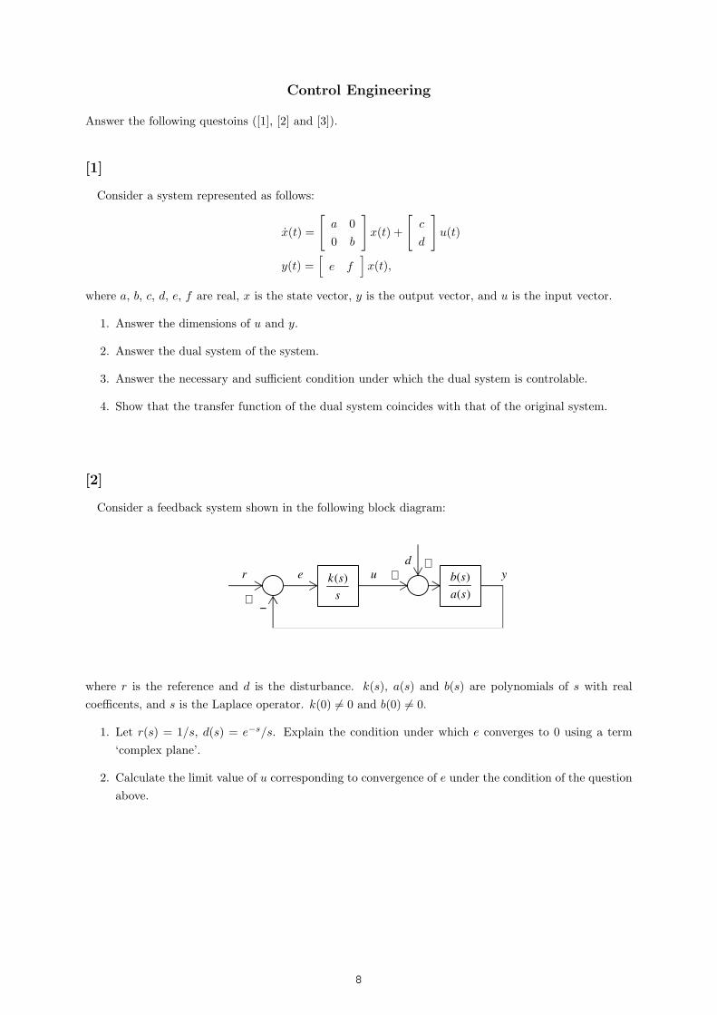
Control Engineering
Answer the following questoins ([1], [2] and [3]).
[1]
Consider a system represented as follows:
x(t) =
[a 00 b
]x(t) +
[c
d
]u(t)
y(t) =[
e f]x(t),
where a, b, c, d, e, f are real, x is the state vector, y is the output vector, and u is the input vector.
1. Answer the dimensions of u and y.
2. Answer the dual system of the system.
3. Answer the necessary and sufficient condition under which the dual system is controlable.
4. Show that the transfer function of the dual system coincides with that of the original system.
[2]
Consider a feedback system shown in the following block diagram:
( )k s
s
( )
( )
b s
a s+
++
−
r e
d
yu
where r is the reference and d is the disturbance. k(s), a(s) and b(s) are polynomials of s with realcoefficents, and s is the Laplace operator. k(0) = 0 and b(0) = 0.
1. Let r(s) = 1/s, d(s) = e−s/s. Explain the condition under which e converges to 0 using a term‘complex plane’.
2. Calculate the limit value of u corresponding to convergence of e under the condition of the questionabove.
8

[3]
Consider a system depicted by the block diagram below. The input to the system is u(t) and the outputis y(t). In the figure, each signal is indicated by its Laplace transform. Here the Laplace transform of anarbitrary signal f(t) is represented by F (s).
1. Define a state variable vector of the system appropriately, and derive a state transition equationand an output equation that describe the system. Here make the dimension of the state variablevector minimal.
2. Determine the BIBO stability of the system.
9

平成 29年度 九州大学大学院システム情報科学府 電気電子工学専攻
修士課程 入学試験問題
専門Ⅱ (Special subjects Ⅱ)
解答上の注意 (Instructions):
1. 問題用紙は、『始め』の合図があるまで開いてはならない.
Do not open this cover sheet until the start of examination is announced.
2. 問題用紙は表紙を含め 17枚、解答用紙は 3枚である.
You are given 17 problem sheets including this cover sheet, and 3 answer sheets.
3. 以下の 3分野から 1分野を選び解答すること.
Select 1 out of the following 3 fields and answer the questions.
分野 field page
1 電磁気学 Electromagnetism 2 ~
2 半導体デバイス Semiconductor device 8 ~
3 計算機工学 Computer engineering 14 ~
4. 解答は解答用紙に記入すること.大問一つあたり一枚の解答用紙を用いよ.スペース
が足りない場合は裏面を用いても良いが,その場合は,裏面に解答があることを明記
すること.
Your answers should be written on the answer sheets. Use one sheet for each
question. You may continue to write your answer on the back of the answer sheets if
you need more space. In such a case, indicate this clearly.
5. 解答用紙の全部に,志望するコース名,選択分野名,受験番号,氏名および問題番号
を記入すること.
Fill in the designated blanks at the top of each answer sheet with the course name,
your selected field name, your examinee number, your name and the question
number.
1
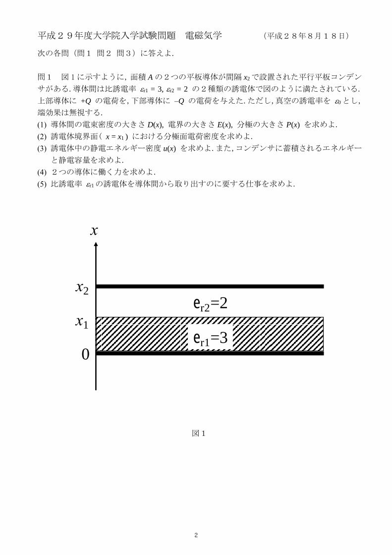
平成29年度大学院入学試験問題 電磁気学 (平成28年8月18日)
次の各問(問1 問2 問3)に答えよ.
問1 図 1に示すように,面積 A の2つの平板導体が間隔 x2で設置された平行平板コンデン
サがある.導体間は比誘電率 r1 = 3, r2 = 2 の2種類の誘電体で図のように満たされている.
上部導体に +Q の電荷を,下部導体に –Q の電荷を与えた.ただし,真空の誘電率を 0とし,
端効果は無視する.
(1) 導体間の電束密度の大きさ D(x), 電界の大きさ E(x), 分極の大きさ P(x) を求めよ.
(2) 誘電体境界面( x = x1 ) における分極面電荷密度を求めよ.
(3) 誘電体中の静電エネルギー密度 u(x) を求めよ.また,コンデンサに蓄積されるエネルギー
と静電容量を求めよ.
(4) 2つの導体に働く力を求めよ.
(5) 比誘電率 r1の誘電体を導体間から取り出すのに要する仕事を求めよ.
図1
x
0
x2
x1
er1=3
er2=2
2

平成29年度大学院入学試験問題 電磁気学 (平成28年8月18日)
問2 同心球殻導体(内側球殻の半径 r1,外側球殻の半径 r2)について以下の問いに答えよ.
(1) 図2 (a)に示すように,両球殻間が導電率 σ0 の物質で満たされている場合,両球殻間の抵
抗 Raを求めよ.
(2) 図2 (b)に示すように,両球殻間の半径 r1 < r < dの領域が導電率 σ1の物質で、半径 d < r < r2
の領域が導電率 σ2 の物質でそれぞれ満たされている場合,両球殻間の抵抗 Rbを求めよ.
(3) 図2 (c)に示すように,両球殻間の右半分の半球殻が導電率 σ1 の物質で、左半分の半球殻
が導電率 σ2 の物質でそれぞれ満たされている場合,両球殻間の抵抗 Rcを求めよ.
図2
3

平成29年度大学院入学試験問題 電磁気学 (平成28年8月18日)
問3 図3に示すように直線導体と一辺が a, b の角型コイルが距離 d 離れて同一平面上に配
置されている.直線導体を固定し直流電流 Idcを流した.全ての領域で透磁率をとする.
(1) コイルの端子 S, T 間を開放した場合,コイルに鎖交する磁束を求めよ.
(2) 端子 S, T 間に抵抗 R を接続し,距離 d が d(t) = d0 + vt となるようにコイルを速度 v で移
動した.ただし,t は時間であり v > 0 とする.この時,コイルに流れる電流 Icoilの大き
さを求めよ.また,電流 Icoil によりコイルに働く磁気力 Fm を求めよ.ただし,電流 Icoil
によって発生する磁界は無視できるとする.
(3) コイルを速度 v で動かすために必要な外力 Fex と外力 Fex が単位時間当たりになす仕事
W を求めよ.また,抵抗 R で消費される電力 P を求め,W と等しいことを示せ.
図3
4
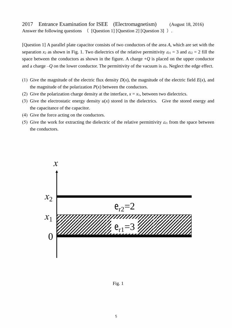
2017 Entrance Examination for ISEE (Electromagnetism) (August 18, 2016)
Answer the following questions ( [Question 1] [Question 2] [Question 3] ).
[Question 1] A parallel plate capacitor consists of two conductors of the area A, which are set with the
separation x2 as shown in Fig. 1. Two dielectrics of the relative permittivity r1 = 3 and r2 = 2 fill the
space between the conductors as shown in the figure. A charge +Q is placed on the upper conductor
and a charge –Q on the lower conductor. The permittivity of the vacuum is 0. Neglect the edge effect.
(1) Give the magnitude of the electric flux density D(x), the magnitude of the electric field E(x), and
the magnitude of the polarization P(x) between the conductors.
(2) Give the polarization charge density at the interface, x = x1, between two dielectrics.
(3) Give the electrostatic energy density u(x) stored in the dielectrics. Give the stored energy and
the capacitance of the capacitor.
(4) Give the force acting on the conductors.
(5) Give the work for extracting the dielectric of the relative permittivity r1 from the space between
the conductors.
Fig. 1
x
0
x2
x1
er1=3
er2=2
5

2017 Entrance Examination for ISEE (Electromagnetism) (August 18, 2016)
[Question 2] A concentric spherical shell electrode system consists of an inner spherical shell (radius
r1) and an outer spherical shell (radius r2).
(1) As shown in Fig. 2 (a), the space between the two spherical shells is filled with material with
electrical conductivity σ0 . Give the electrical resistance Ra between the two spherical shells.
(2) As shown in Fig. 2 (b), the space between the two spherical shells is divided into two regions
according to radial distance. The inner region (r1 < r <d) is filled with material with electrical
conductivity σ1 , whereas the outer region (d < r < r2) is filled with material with electrical
conductivity σ2 . Give the electrical resistance Rb between the two spherical shells.
(3) As shown in Fig. 2 (c), the space between the two spherical shells is divided into two
hemispherical shells. The right hemispherical shell is filled with material with electrical
conductivity σ1 , whereas the left hemispherical shell is filled with material with electrical
conductivity σ2 . Give the electrical resistance Rc between the two spherical shells.
Fig. 2
6
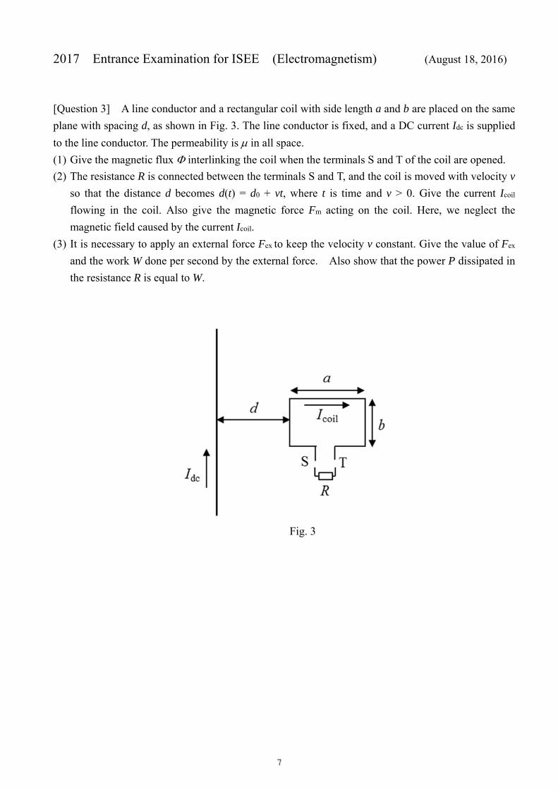
2017 Entrance Examination for ISEE (Electromagnetism) (August 18, 2016)
[Question 3] A line conductor and a rectangular coil with side length a and b are placed on the same
plane with spacing d, as shown in Fig. 3. The line conductor is fixed, and a DC current Idc is supplied
to the line conductor. The permeability is in all space.
(1) Give the magnetic flux interlinking the coil when the terminals S and T of the coil are opened.
(2) The resistance R is connected between the terminals S and T, and the coil is moved with velocity v
so that the distance d becomes d(t) = d0 + vt, where t is time and v > 0. Give the current Icoil
flowing in the coil. Also give the magnetic force Fm acting on the coil. Here, we neglect the
magnetic field caused by the current Icoil.
(3) It is necessary to apply an external force Fex to keep the velocity v constant. Give the value of Fex
and the work W done per second by the external force. Also show that the power P dissipated in
the resistance R is equal to W.
Fig. 3
7

平成 29年度 修士課程入学試験
半導体デバイス
次の各問( 1 2 3 )に答えよ.
1 半導体結晶(A, B, C)に関する下記の設問に答えよ.ただし,半導体結晶 A, B, C はすべ
て p 型伝導を示し,室温における正孔密度は,それぞれ p, p, 100 p である.A のバンド
ギャップは,B および C よりも大きく,B のバンドギャップは C と等しい.また,A, B,
C の伝導帯および価電子帯の有効状態密度はすべて等しい.
(1) 半導体結晶 A および B について,正孔密度の温度依存性を示すグラフを模式的に
描け.グラフには,キャリヤ密度 C の対数表示を縦(y)軸,絶対温度 T の逆数を横
(x)軸に取り,正孔密度を実線で描け.また,温度依存性の様子に応じ,低温,中
温,高温の領域を図示せよ.
(2) 半導体結晶 A の自由電子密度の温度依存性を,前項(1)で求めたグラフに破線で示
せ.
(3) 中温領域において,半導体結晶 A および C の正孔移動度の温度依存性は,それぞ
れ,温度 TA及び TCでピークをもつ山型の曲線となる.正孔移動度 μの対数表示を
縦(y)軸,絶対温度 T の対数表示を横(x)軸に取り,A および C の移動度の温度変化
を模式的に比較して示せ.ただし,格子散乱および不純物散乱で規定される移動
度 μLおよび μIは,それぞれ次式で与えられる.
2/3 TPL ,
2/3TN
Q
II
ここで,P,Q は定数であり,半導体結晶 A, B, C で全て等しい.また,NIはイオ
ン化した不純物の密度である.
(4) 中温領域内の低温側(T<TA)における半導体結晶 A の抵抗率は,半導体結晶 C と比
べて大きいか,小さいか,または同等か?理由とともに答えよ.
(5) 中温領域内の高温側(T>TC)における半導体結晶 A の抵抗率は,半導体結晶 C と比
べて大きいか,小さいか,または同等か?理由とともに答えよ.
8

2
p型(アクセプター密度: NA)と n型(ドナー密度: ND)のシリコン(Si)からなる pn接合
に関して,下記の設問に答えよ.
(1) p 型 Si および n 型 Si のフェルミ・エネルギーの位置が,それぞれ,価電子帯の頂
(EV)から 0.30eV だけ上(EV+0.30eV),および伝導帯の底(EC)から 0.15eV だけ下
(EC−0.15eV)であった.この時の pn 接合の拡散電位 Vdを求めよ.ただし,Si のバン
ドギャップは 1.12eV とせよ.
(2) p 型 Si のアクセプター密度を 100 NA,n 型 Si のドナー密度を 10 NDに増加させる.
これにより,pn 接合の拡散電位は増加するか,減少するか?理由と共に答えよ.
(3) 順方向バイアス状態(バイアス電圧 VF)及び逆方向バイアス状態(バイアス電圧 VR)
の pn接合(p型 Si のアクセプター密度: NA, n型 Si のドナー密度:ND)のバンド図を描
け.バンド図には,価電子帯の頂 EV,伝導帯の底 EC,フェルミ・エネルギー EF,
pn 接合の拡散電位 Vdを記載すること.さらに,p 型領域および n 型領域の空乏層
端の位置 −xp,xn を示せ.ただし,電気素量を q とし,pn 接合界面の位置を x=0
とせよ.
(4) 逆方向バイアス状態のバイアス電圧 VRの大きさを上記(3)より増加した.接合界面
から p 型側への空乏層領域の幅 xp,n 型側への空乏層領域の幅 xnは,いずれが大き
く増加するか?理由と共に答えよ.
(5) 逆方向バイアス電圧 VRを印加したまま,pn 接合の温度を上昇する.pn 接合を流れ
る電流は増えるか,減るか?理由と共に答えよ.
9
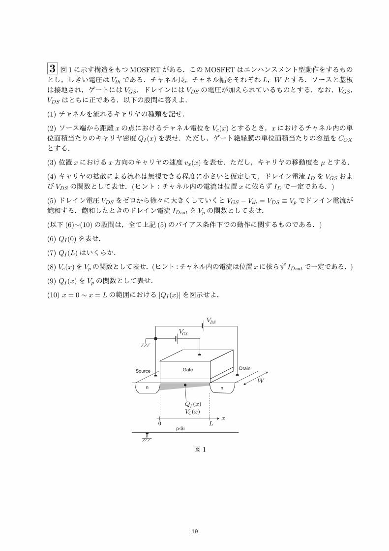
3 図 1に示す構造をもつMOSFETがある.このMOSFETはエンハンスメント型動作をするものとし,しきい電圧は Vth である.チャネル長,チャネル幅をそれぞれ L,W とする.ソースと基板は接地され,ゲートには VGS,ドレインには VDS の電圧が加えられているものとする.なお,VGS,VDS はともに正である.以下の設問に答えよ.
(1) チャネルを流れるキャリヤの種類を記せ.
(2) ソース端から距離 xの点におけるチャネル電位を Vc(x)とするとき,xにおけるチャネル内の単位面積当たりのキャリヤ密度QI(x)を表せ.ただし,ゲート絶縁膜の単位面積当たりの容量を COX
とする.
(3) 位置 xにおける x方向のキャリヤの速度 vx(x)を表せ.ただし,キャリヤの移動度を µとする.
(4) キャリヤの拡散による流れは無視できる程度に小さいと仮定して,ドレイン電流 IDを VGS および VDS の関数として表せ.(ヒント:チャネル内の電流は位置 xに依らず IDで一定である.)
(5) ドレイン電圧 VDS をゼロから徐々に大きくしていくと VGS − Vth = VDS ≡ Vpでドレイン電流が飽和する.飽和したときのドレイン電流 IDsatを Vpの関数として表せ.
(以下 (6)∼(10)の設問は,全て上記 (5)のバイアス条件下での動作に関するものである.)
(6) QI(0)を表せ.
(7) QI(L)はいくらか.
(8) Vc(x)をVpの関数として表せ.(ヒント:チャネル内の電流は位置xに依らず IDsatで一定である.)
(9) QI(x)を Vpの関数として表せ.
(10) x = 0 ∼ x = Lの範囲における |QI(x)|を図示せよ.
n n
SourceDrainGate
0 Lx
W
V (x)C
VGS
VDS
p-Si
Q (x) I
図 1
10

2017 Entrance Examination
Semiconductor devices
Answer the following questions ( 1 2 3 ).
1
Answer the following questions concerning semiconductor crystals A, B, and C. All of
semiconductor crystals A, B, and C show p-type conduction and have hole concentration of p, p,
and 100 p, respectively, at room temperature. The band gap of A is larger than those of B and C,
where the band gap of B is the same as that of C. In addition, all of effective density of states of
the conduction bands and valence bands of A, B, and C are the same value.
(1) Draw schematically a graph showing the temperature dependence of hole concentration in
semiconductor crystals A and B. In the graph, take the logarithmic carrier concentration as
the y-axis and the inverse of the absolute temperature (T) as the x-axis, and draw the hole
concentration with solid lines. In addition, indicate the low, middle, and high temperature
regions, based on the temperature dependence.
(2) Draw the temperature dependence of free electron concentration in semiconductor crystals A
with a broken line in the graph obtained by the previous question (1).
(3) The temperature dependence of hole mobility in semiconductor crystals A and C show
convex curves with peaks at temperatures TA and TC, respectively. Draw schematically the
temperature dependence of the hole mobility in A and C, taking the logarithmic hole mobility
as the y-axis and the logarithmic absolute temperature T as the x-axis. The mobilities
limited by the lattice scattering L and impurity scattering I are given by the following
equations:
2/3 TPL ,
2/3TN
Q
II ,
where P and Q are constant and have the same values for semiconductor crystals A, B, and C.
NI is the ionized impurity concentration.
(4) At a lower temperature (T<TA) in the middle temperature region, is the resistivity of
semiconductor crystal A larger, smaller, or almost equal compared with that of semiconductor
crystal C? Answer with the reason.
(5) At a higher temperature (T>TC) in the middle temperature region, is the resistivity of
semiconductor crystal A larger, smaller, or almost equal compared with that of semiconductor
crystal C? Answer with the reason.
11

2 Answer the following questions concerning a pn junction diode, composed of p-type
(acceptor concentration: NA) and n-type Si (donor concentration: ND).
(1) The energy positions of the Fermi level in the p-type and n-type Si are above the top of the
valence band (EV) by 0.30eV (EV +0.30eV) and below the bottom of the conduction band
(EC) by 0.15eV (EC−0.15eV), respectively. Evaluate the built-in potential Vd of the pn
junction. Assume that the energy band gap of Si is 1.12eV.
(2) The acceptor concentration in p-type Si and the donor concentration in n-type Si are
increased to 100 NA and 10 ND, respectively. Does the built-in potential increase or decrease?
Answer with the reason.
(3) Draw a band diagram for the pn junction (acceptor concentrations in p-type Si: NA, donor
concentration in n-type Si: ND) under the forward bias condition (bias voltage: VF) and that
under the reverse bias condition (bias voltage: VR). The energy positions of the top of the
valence band EV, the bottom of the conduction band EC, the Fermi energy EF, and the built-in
potential Vd should be given in the drawing. Moreover, show the edge positions −xp and xn of
the depletion region in p-type and n-type semiconductors, respectively. Here, the elementary
charge is represented as q, and x=0 at the pn junction interface.
(4) The absolute value of the reverse bias VR is increased compared with the previous question
(3). Which increases more largely, xp or xn? Answer with the reason.
(5) Under the reverse bias VR, the temperature of the pn junction is increased. Does the current
through the pn junction increase or decrease? Answer with the reason.
12

3 Consider a MOSFET shown in Fig. 1. The MOSFET is enhancement mode type having
the threshold voltage Vth. The channel length and the channel width are L and W , respectively.
The source and the substrate are grounded. The gate and the drain are biased at VGS and VDS ,
respectively, where VGS and VDS are both positive. Answer the following questions.
(1) What is the carrier flowing in the channel?
(2) Express the carrier density per unit area at position x, QI(x), using the channel potential Vc(x).
Use COX , capacitance of the gate insulator per unit area, to answer.
(3) Express the speed of carriers along the x direction at position x, vx(x). Use carrier mobility µ
to answer.
(4) Derive the drain current ID as a function of VGS and VDS . Assume that diffusion of carriers is
negligiblly small.(Hint: Current flowing in the channel is independent of x and equals to ID.)
(5) When the drain voltage VDS is incresed from zero, drain current saturates at VGS − Vth =
VDS ≡ Vp. Derive the saturated drain current IDsat as a function of Vp.
(The following questions (6) - (10) are all under the bias condition described in the question (5). )
(6) Express QI(0).
(7) How much is QI(L)?
(8) Express Vc(x) as a function of Vp. (Hint: Current flowing in the channel is independent of x
and equal to IDsat.)
(9) Derive QI(x) as a function of Vp.
(10) Draw |QI(x)| in the range from x = 0 to x = L.
n n
SourceDrainGate
0 Lx
W
V (x)C
VGS
VDS
p-Si
Q (x) I
Fig. 1
13

【計算機工学 (Computer Engineering )分野】
次の各問い(【問 1】~【問 3】)に答えよ.
【問 1】クイックソートの擬似コードが図 1のように記述されている.このとき,次の各問いに
答えよ.
QUICKSORT(A, p, r)
1 if p < r
2 then q ←PARTITION(A, p, r)
3 QUICKSORT(A, p, q)
4 QUICKSORT(A, q + 1, r)
PARTITION(A, p, r)
1 x← A[p]
2 i← p− 1
3 j ← r + 1
4 while TRUE
5 do repeat j ← j − 1
6 until A[j] ≤ x
7 repeat i← i+ 1
8 until A[i] ≥ x
9 if i < j
10 then exchange values A[i]↔ A[j]
11 else return j
図 1: クイックソートの擬似コード
(1) 配列A(= [4, 3, 7, 8, 6, 2]) に対して,PARTITION(A, 1, 6)を実行した場合に PAR-
TITIONの返す値, および実行後の配列の状態を示せ.この記法では,配列のイン
デックスは 1から始まる(上の例では,A[1]=4となる)ことに注意.
(2) すべての 6要素の配列に対して,QUICKSORTが終了するまでに,手続き PARTI-
TIONが 呼び出される回数の最小値を求めよ.
(3) 安定なソーティングアルゴリズムでは,同じ値を有する複数の要素に関して,元の
列の順序が常に保存される.QUICKSORTは安定でないことを示せ.
(4) q < rが必ず成立する理由を簡潔に示せ.
14
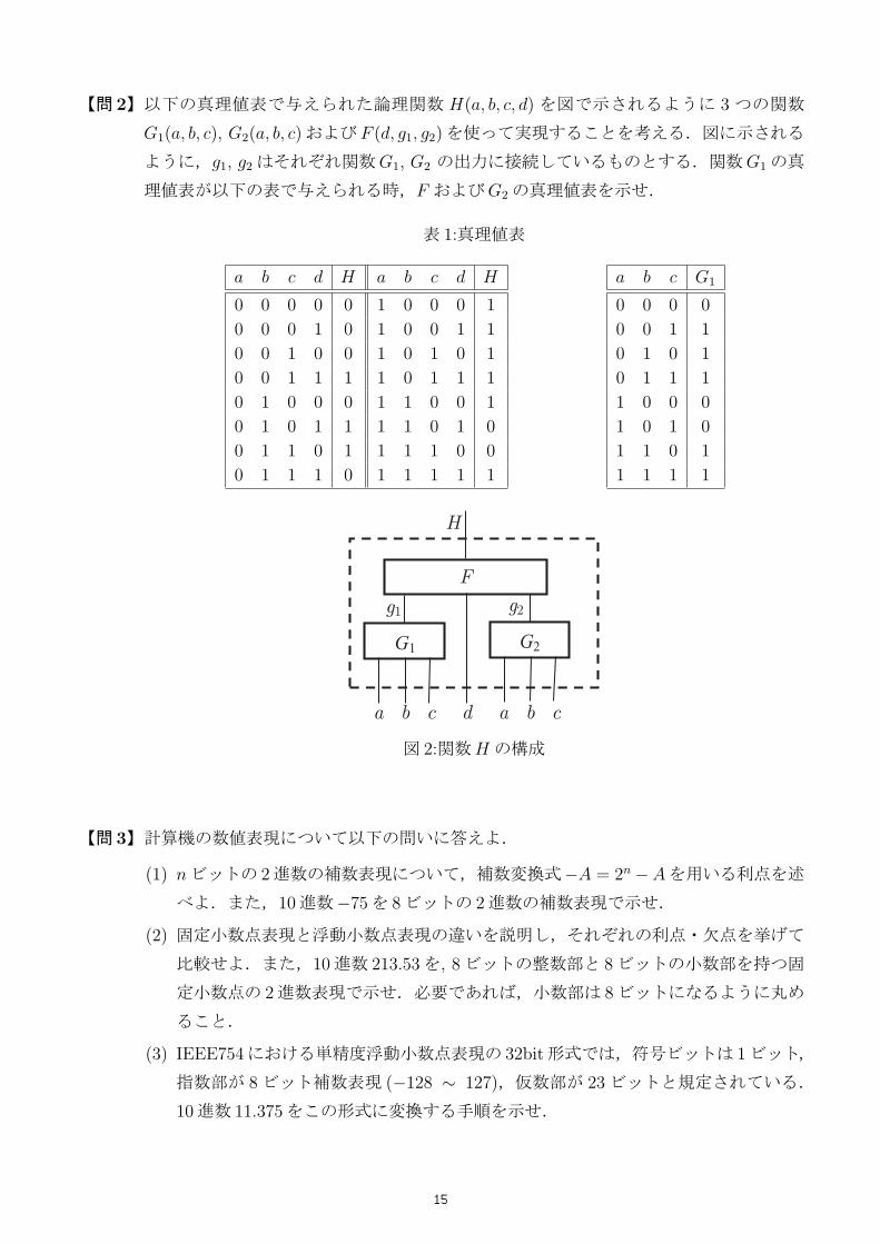
【問 2】以下の真理値表で与えられた論理関数 H(a, b, c, d) を図で示されるように 3 つの関数
G1(a, b, c), G2(a, b, c)および F (d, g1, g2)を使って実現することを考える.図に示される
ように,g1, g2はそれぞれ関数G1, G2 の出力に接続しているものとする.関数G1の真
理値表が以下の表で与えられる時,F およびG2の真理値表を示せ.
表 1:真理値表
a b c d H a b c d H
0 0 0 0 0 1 0 0 0 1
0 0 0 1 0 1 0 0 1 1
0 0 1 0 0 1 0 1 0 1
0 0 1 1 1 1 0 1 1 1
0 1 0 0 0 1 1 0 0 1
0 1 0 1 1 1 1 0 1 0
0 1 1 0 1 1 1 1 0 0
0 1 1 1 0 1 1 1 1 1
a b c G1
0 0 0 0
0 0 1 1
0 1 0 1
0 1 1 1
1 0 0 0
1 0 1 0
1 1 0 1
1 1 1 1
H
F
g1
G1 G2
g2
a b c a b cd
図 2:関数Hの構成
【問 3】計算機の数値表現について以下の問いに答えよ.
(1) nビットの 2進数の補数表現について,補数変換式−A = 2n −Aを用いる利点を述べよ.また,10進数−75を 8ビットの 2進数の補数表現で示せ.
(2) 固定小数点表現と浮動小数点表現の違いを説明し,それぞれの利点・欠点を挙げて
比較せよ.また,10進数 213.53を, 8ビットの整数部と 8ビットの小数部を持つ固
定小数点の 2進数表現で示せ.必要であれば,小数部は 8ビットになるように丸め
ること.
(3) IEEE754における単精度浮動小数点表現の 32bit形式では,符号ビットは 1ビット,
指数部が 8ビット補数表現 (−128 ∼ 127),仮数部が 23ビットと規定されている.
10進数 11.375をこの形式に変換する手順を示せ.
15

Answer the following questions (【Q1】-【Q3】).
【Q1】A pseudo code for quicksort can be described as shown in Fig. 1.
QUICKSORT(A, p, r)
1 if p < r
2 then q ←PARTITION(A, p, r)
3 QUICKSORT(A, p, q)
4 QUICKSORT(A, q + 1, r)
PARTITION(A, p, r)
1 x← A[p]
2 i← p− 1
3 j ← r + 1
4 while TRUE
5 do repeat j ← j − 1
6 until A[j] ≤ x
7 repeat i← i+ 1
8 until A[i] ≥ x
9 if i < j
10 then exchange values A[i]↔ A[j]
11 else return j
Fig. 1: Pseudo code for quicksort
(1) Let us assume PARTITION(A, 1, 6) is applied to array A(= [4, 3, 7, 8, 6, 2]). Note
that we assume the first element of the array is A[1], i.e., A[1] = 4 in this case.
Describe the return value of PARTITION and the state of array A.
(2) Find the smallest total number of calls of PARTITION in order to complete QUICK-
SORT for any array of size 6.
(3) A sorting algorithm is stable if for multiple elements with the same value, the order
of the original input is always preserved. Show that QUICKSORT is not stable.
(4) Describe the reason why q < r always holds.
16
【Q2】Let H(a, b, c, d) be a logic function whose truth table is shown below. Consider that
H is composed of other subfunctions G1(a, b, c), G2(a, b, c) and F (d, g1, g2) as shown in
the figure below. Inputs of F , g1 and g2 are connected to the output of G1 and G2,
respectively. When the truth table for G1 is given below, show the truth tables of F and
G2.
Table 1:Truth tables
a b c d H a b c d H
0 0 0 0 0 1 0 0 0 1
0 0 0 1 0 1 0 0 1 1
0 0 1 0 0 1 0 1 0 1
0 0 1 1 1 1 0 1 1 1
0 1 0 0 0 1 1 0 0 1
0 1 0 1 1 1 1 0 1 0
0 1 1 0 1 1 1 1 0 0
0 1 1 1 0 1 1 1 1 1
a b c G1
0 0 0 0
0 0 1 1
0 1 0 1
0 1 1 1
1 0 0 0
1 0 1 0
1 1 0 1
1 1 1 1
H
F
g1
G1 G2
g2
a b c a b cd
Fig. 2: Structure of function H
【Q3】Answer following questions about numerical format of computer.
(1) The conversion equation −A = 2n−A is used in binary complement expression of n
bits length. Explain the advantages of the complement expression. Convert decimal
value −75 into the 8-bit binary complement expression.
(2) Explain the differences between fixed point expression and floating point expression.
Give their respective advantages and disadvantages and compare them. Convert
decimal value 213.53 into binary fixed point expression that has 8 bits for integer
part and 8 bits for fractional part. Round the fractional part to 8 bits if needed.
(3) The single precision 32-bit IEEE754 format adopts 1 bit for sign, 8 bits for comple-
ment expression of exponent (−127 - 128), and 23 bits for mantissa. Describe the
conversion process of the decimal value 11.375 into the IEEE754 format.
17